1
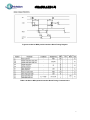
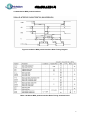
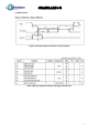
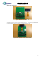
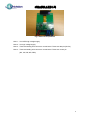
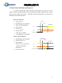
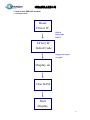
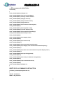
悠景科技股份有限公司
UG-2864ASYCG01
UG-2864ASOCG01
Evaluation Kit User Guide
Writer: James Wang
Email: [email protected]
Version: Preliminary
1
悠景科技股份有限公司
Contents
1. REVISION HISTORY……………………………………………………………………………...3
2. EVK Schematic……………………………………………………………………………………..4
3. Symbol define………………………………………………………………………………………5
4. TIMMING CHARACTERISTICS…………………………...……………………………………...6
4.1 80-Series MPU parallel Interface ………………………………………………………..6
4.2 6800-Series MPU parallel Interface …………………………………………………….8
4.3 SPI Interface ………………………………………………………………………………..9
5. EVK use introduction………………………………………………………………………..…..10
6.Power down and Power up Sequence……………………………………………………...…12
7. How touseSSD1305module…………………………………………………………………….13
7.1 Initial Step Flow…………………………………………………………………………...14
7.2 RD recommend Initial Code for 80 Interface…………………………………………14
7.2.1 Sub Function for 80 Interface………………………………………………….14
2
悠景科技股份有限公司
1. REVISION HISTORY
Date
2007/11/28
Page
Contents
Version
Preliminary
Preliminary 0.0
3
悠景科技股份有限公司
2. EVK Schematic
4
悠景科技股份有限公司
3. Symbol define
VCC : Power supply for panel driving voltage.
VSS:This is ground pin.
VDD:Power supply for core logic operation.
VDDIO:Power supply for interface logic level.
BS0~BS2:MUC bus interface selection pin(BS0 pulled LOW in internal).
CS:This pin is chip select input(active LOW).
RES:This pin is reset signal input(active LOW).
D/C:This is DATA/COMMAND control pin. When it is Pulled HIGH, the data at D[0~7] is
treated as data. When it is pulled LOW, the data at D[0~7] will be transferred to
the command register.
In I2C mode, this pin acts as SA0 for slave address select.
R/W:This is read/write control input pin connecting to the MCU interface.
When interface to a 6800-series microprocessor , Read mode will be carried out
when this pin is pulled HIGH and write mode when low .
When interface to an 8080-microprocessor , this pin when be the data Write
input.
When serial interface is selected, this pin must be connected to Vss.
E/RD:When interface to a 6800-series microprocessor , this pin will be used as the
Enable(E) signal.
When interface to an 8080-microprocessor , this pin receives the
Read(RD#)signal.
D0~D7:These are 8-bit bi-directional data bus to be connected to the microprocessor’s
data bus.
When serial interface mode is selected, D0(SCLK) will be the serial clock
input,D1(SDIN) will be the serial data input,D2 should be left opened.
When I2C mode is selected,D1(SDAin) AND D2(SDAout) should be tied together,D0(SCL)
is the I2Cclock input
IREF:This is segment output current reference pin.
VCOMH:This pin for COM signal deselected level voltage.
5
悠景科技股份有限公司
4.TIMMING CHARACTERISTICS
4.1 80-Series MPU parallel Interface
Figure 1 80-Series MPU parallel Interface Write Timing Diagram
Table 1 80-Series MPU parallel Interface Write Timing Characteristics
6
悠景科技股份有限公司
Figure 2 80-Series MPU parallel Interface Read Timing Diagram
Table 2 80-Series MPU parallel Interface Read Timing Characteristics
7
悠景科技股份有限公司
4.2 6800-Series MPU parallel Interface
Figure 3 68-Series MPU parallel Interface Write Timing Diagram
Table 3 68-Series MPU parallel Interface Write Timing Characteristics
8
悠景科技股份有限公司
4.3 SPI Interface
Figure 4 Serial peripheral interface Timing Diagram
Table 4 Serial peripheral interface Timing Characteristics
9
悠景科技股份有限公司
5.EVK use introduction
Module
Figure 5 EVK PCB and OLED Module
Interface select
UG-2864ASYCG01 is COG type module, please refer to Fig5, Fig6.User can use leading wire
to connect EVK with customer’s system. The example shows as Fig7.
Figure 6 The combination of the module and EVK
10
悠景科技股份有限公司
Fig 7 EVK with test platform
Note 1:It is OLED high voltage supply.
Note 2:It is logic voltage supply.
Note 3:Those are leading wire connect to control board. Those are data pin.(D0-D7)
Note 4:Those are leading wire connect to control board. Those are control pin.
(DC, CS, RD, WR, RES)
11
悠景科技股份有限公司
6. Power down and Power up Sequence
To protect OLED panel and extend the panel lifetime, the driver IC power
up/down routine should include a delay period between high voltage and low voltage
power sources during turn on/off. Such that panel has enough time to charge up or
discharge before/after operation.
Power up Sequence:
1.
2.
3.
4.
5.
6.
7.
Power up VDD
Send Display off command
Driver IC Initial Setting
Clear Screen
Power up VDDH
Delay 100ms
(when VDD is stable)
VDD on
VCC on
Display on
VCC
VDD
VSS/Ground
Send Display on command
Power down Sequence:
1. Send Display off command
2. Power down VDDH
3. Delay 100ms
(when VDDH is reach 0 and
panel is completely
discharges)
4. Power down VDD
Display off
VCC off
VDD off
VCC
VDD
VSS/Ground
12
悠景科技股份有限公司
7. How to use SSD1305 module
7.1 Initial Step Flow
Reset
Driver IC
RES=0
Delay 10ms
RES=1
Driver IC
Initial Code
Suggest all register
set again
Display on
Clear RAM
Start
Display
13
悠景科技股份有限公司
7.2 RD recommends Initial Code:
void initial()
{
write_command(0xae);//(display on)
write_command(0x00);//set low column address
write_command(0x10);//set high column address
write_command(0x40);//(display start set)
write_command(0x2e);//(stop horzontal scroll)
write_command(0xb0);//(page address)
write_command(0x81);//(set contrast control register)
write_command(0x7f);
write_command(0xa1);//(set segment re-map)
write_command(0xa4);//(normal display mode)
write_command(0xa6);//(set normal/inverse display)
write_command(0xa8);//(set multiplex ratio)
write_command(0x3f);
write_command(0xd3);//(set display offset)
write_command(0x00);
write_command(0xad);//(set dc-dc on/off)
write_command(0x8e);//
write_command(0xc8);//(set com output scan direction)
write_command(0xd5);//(set display clock divide ratio/oscillator/frequency)
write_command(0xf0);//
write_command(0xd8);//(set area color mode on/off & low power display mode )
write_command(0x05);//
write_command(0xd9);//(set pre-charge period)
write_command(0xc2);
write_command(0xda);//(set com pins hardware configuration)
write_command(0x12);
write_command(0xdb);//(set vcom deselect level)
write_command(0x08);
write_command(0xaf);//(display on)
}
WRITE DATA & COMMAND SUB FUNCTION
void write_command(unsigned char aa)
{
IOCLR = 0x000000ff;
IOSET = RD_IN;//RD=1
14
悠景科技股份有限公司
IOCLR = DC_IN;//DC=0
IOCLR = CS_IN;//CS=0
IOCLR = WR_IN;//WR=0
IOSET = aa;//--------input command
IOSET = WR_IN;//WR=1
IOSET = CS_IN;//CS=1
IOCLR = RD_IN;
}
void write_data(unsigned char bb)
{
IOCLR = 0x000000ff;
IOSET = RD_IN;//RD=1
IOSET = DC_IN;//DC=1
IOCLR = CS_IN;//CS=0
IOCLR = WR_IN;//WR=0
IOSET = bb; //--------input data
IOSET = WR_IN;//WR=1
IOSET = CS_IN;//CS=1
}
Note:RD recommends Initial code and sub function for 8080 series CPU
interface.
15