1
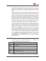
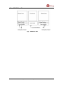
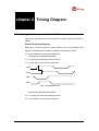
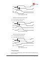
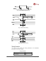
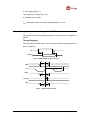
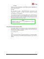
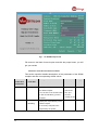
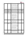
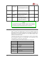
VeriSilicon SMIC 0.18µm High-Speed / Low Leakage Synchronous Single-Port/Dual-Port SRAM Compiler User’s Guide Trademark Acknowledgments VeriSilicon & the VeriSilicon logo are the trademarks of VeriSilicon Microelectronics (Shanghai) Co., Ltd. All other products and company names mentioned may be the trademarks of their respective owners. 2002 VeriSilicon Microelectronics (Shanghai) Co., Ltd. All rights reserved. Printed in P.R.China. VeriSilicon Microelectronics (Shanghai) Co., Ltd. reserves all its copy rights and other intellectual property rights, ownership, powers, benefits and rights arising or to arise from this manual. All or part of the contents of this manual may be changed by VeriSilicon Microelectronics (Shanghai) Co., Ltd. without notice at any time for any reason, including but not limited to improvement of the product relating hereto. VeriSilicon Microelectronics (Shanghai) Co., Ltd. shall not undertake or assume any obligation, responsibility or liability arising out of or in respect of the application or use of the product described herein, except for reasonable, careful and normal uses. Nothing, whether in whole or in part, within this manual can be reproduced, duplicated, copied, changed or disposed of in any form or by any means without prior written consent by VeriSilicon Microelectronics (Shanghai) Co., Ltd.. VeriSilicon Microelectronics (Shanghai) Co., Ltd. 3F, Building 1, No.200, Zhangheng Road, Zhangjiang Hi-Tech Park, Pudong New Area, Shanghai 201204, P. R. China Tel : +86-21-5131-1118 Fax : +86-21-5131-1119 Web : http://www.verisilicon.com 3 Contents Chapter 1 Introduction 1.1 1.2 1.3 1.4 1.5 1.6 1.7 Chapter 2 2.2 Chapter 3 Compiler Description..................................................4 Features.....................................................................4 Operating Conditions .................................................4 Write Mask Description ..............................................5 Pin Descriptions .........................................................5 Parameter Range.......................................................6 SRAM Floor Plan .......................................................7 Timing Diagram 2.1 3.6 8 Timing Specifications for Dual-Port SRAM ................8 Clock Contention Diagram ........................8 Timing Diagrams .......................................9 Timing Parameters..................................10 Power Parameters ..................................11 Timing Specifications for Single-Port SRAM ............12 Timing Diagrams .....................................12 Timing Parameters..................................13 Power Parameters ..................................13 Using the SRAM Compiler 3.1 3.2 3.3 3.4 3.5 4 15 System Requirement ...............................................15 Software Environment..............................................15 Installing SRAM Compiler ........................................15 Inputs and Outputs...................................................16 Getting Started.........................................................17 Using Shell Commands...........................17 Using Graphical User Interface (GUI) .....18 Generating the Outputs............................................21 VeriSilicon SMIC 0.18um LL Syn. SP/DP SRAM Compiler User's Guide Introduction 4 chapter 1 Introduction 1.1 Compiler Description VeriSilicon SMIC 0.18µm High-Speed Synchronous Single-Port/Dual-Port SRAM compiler optimized for Semiconductor Manufacturing International Corporation (SMIC) 0.18µm Logic 1P6M Salicide 1.8/3.3V Low Leakage process can flexibly generate memory blocks by a friendly GUI or shell commands. The compiler supports comprehensive range of word and bits. While satisfying speed and power requirements, it was optimized for area efficiency. VeriSilicon SMIC Synchronous Single-Port/Dual-Port SRAM compiler uses four layers within the blocks and supports metal 4, 5, or 6 as the top metal. Dummy bit cells are designed in with the intention to enhance reliability. 1.2 Features • • • • • • • • 1.3 Single or Dual Read/Write Ports High Density High Speed Size Sensitive Self-time Delay for Fast Access Time Automatic Power Down Tri-state Output Write mask function Low Leakage Operating Conditions The following table gives the recommended operating conditions for memory blocks generated by SRAM compiler: Recommended Operating Conditions Operating Conditions Parameter Rating Supply Voltage 1.8V 1.62V to 1.98V Temperature 25ºC 0ºC to 125ºC VeriSilicon SMIC 0.18um LL Syn. SP/DP SRAM Compiler User's Guide Introduction 5 1.4 Write Mask Description The SRAM compiler supports write mask selection. When write mask are selected to off, the SRAM works at normal mode without write mask. When write mask are selected to on, the SRAM compiler works at write mask mode. If Single-Port SRAM works at normal mode, all of the data will be written into the memory when CEN is low and WE is high. If Single-Port SRAM works at write mask mode, the data input bus DIN[i:0] will be partitioned into several groups which enabled by write enable bus WE[j:0], Each group data inputs are enabled by corresponding write enable pin separately. For example, if a single port SRAM with 16 bits is selected to write mask mode, and the write mask group is 4, then write enable bus will be WE[3:0], and DIN[3:0] will be controlled by WE[0], DIN[7:4] will be controlled by WE[2], DIN[11:8] will be controlled by WE[2], DIN[15:12] will be controlled by WE[3] separately. If Dual-Port SRAM works at normal mode, all of the data in port A/B will be written into the memory when CENA/CENB is low and WEA/WEB is high. If Dual-Port SRAM works at write mask mode, the data input bus DAIN[i:0]/ DBIN[i:0] will be partitioned into several groups which enabled by write enable bus WEA[j:0]/WEB[j:0], each group data inputs are enabled by corresponding write enable pin separately. For example, if a dual port SRAM with 16 bits is selected to write mask mode, and the write mask group is 4, then write enable bus will be WEA[3:0]/WEB[3:0], and DAIN[3:0]/DBIN[3:0] will be controlled by WEA[0]/WEB[0], DAIN[7:0]/DBIN[7:4] will be controlled by WEA[2]/WEB[2], DAIN[11:8]/DBIN[11:8] will be controlled by WEA[2]/WEB[2], DAIN[15:12]/DBIN[15:12] will be controlled by WEA[3]/ WEB[3] separately. 1.5 Pin Descriptions The following table gives detailed information of pin descriptions for single-port SRAM (Bus index descending ordered): Pin Description DOUT[i] Data output AD[i] Address input CEN Chip enable input, low enable CLK CLK input, positive edge active DIN[i] Data input OE Output enable, high enable WE Write or Read control input, Write high enable, Read low enable The following table gives detailed information of pin descriptions for VeriSilicon SMIC 0.18um LL Syn. SP/DP SRAM Compiler User's Guide Introduction 6 dual-port SRAM (Bus index descending ordered): 1.6 Pin Description DAOUT[i] A port data output DBOUT[i] B port data output ADA[i] A port address input ADB[i] B port address input CENA A port chip enable input, low enable CENB B port chip enable input, low enable CLKA A port CLK input, positive edge active CLKB B port CLK input, positive edge active DAIN[i] A port data input DBIN[i] B port data input OEA A port output enable, high enable OEB B port output enable, high enable WEA A port Write or Read control input, Write high enable, Read low enable WEB B port Write or Read control input, Write high enable, Read low enable Parameter Range Parameter Range Memory Array Range 4 to 512k Bits Mux4: 2 to 256 Bits, Increments of 1 Data Width Mux8: 2 to 128 Bits, Increments of 1 Mux16: 2 to 64 Bits, Increments of 1 Mux4: 2 to 2048 Words, Increments of (2 X 4) SRAM Address Depth Mux8: 2 to 4096 Words, Increments of (2 X 8) Mux16: 2 to 8192 Words, Increments of (2 X 16) The following list the changes of width and height when column mux is set to different values. Suppose column mux is 16, the width and height is a standard. Width Height 4 1/4 4 8 1/2 2 16 1 1 Column Mux Top Metal Output Drive Strength m4, m5 or m6 The same drive as INVHD8X cell in VeriSilicon SMIC 0.18µm High-Density Standard Cell Library VeriSilicon SMIC 0.18um LL Syn. SP/DP SRAM Compiler User's Guide Introduction 7 1.7 SRAM Floor Plan Fig.1 SRAM Floor Plan VeriSilicon SMIC 0.18um LL Syn. SP/DP SRAM Compiler User's Guide Introduction 8 chapter 2 Timing Diagram 2.1 Timing Specifications for Dual-Port SRAM This section specifies the timing specifications of the synchronous dual-port SRAM. Clock Contention Diagram When port A and B access the same address, the clock contention will happen. The detail clock contention diagrams are shown as follows: tcc is clock collision time reported in datasheet. First read one port then write the other If t > tcc (see Fig.2) write and read are both OK. If t < tcc (see Fig.2) write is OK but read fails. CLKA t CLKB WEA WEB Fig.2 First read then write First write one port then read the other If t > tcc (see Fig.3) write and read are both OK. If t < tcc (see Fig.3) write is OK but read fails. VeriSilicon SMIC 0.18um LL Syn. SP/DP SRAM Compiler User's Guide Timing Diagram 9 CLKA t CLKB WEA WEB Fig.3 First write then read First write one port then write from the other If t > tcc (see Fig.4) both write are OK. If t < tcc (see Fig.4) both write fail. CLKA t CLKB WEA WEB Fig.4 First write then write First read one port then read the other If t > tcc (see Fig.5) both read are OK. If t < tcc (see Fig.5) both read are OK. CLKA t CLKB WEA WEB Fig.5 First read then read Timing Diagrams The synchronous SRAM write, read and output enable timing diagrams are shown as follows: VeriSilicon SMIC 0.18um LL Syn. SP/DP SRAM Compiler User's Guide Timing Diagram 10 OEA OEB tlz thz DAOUT[i] DBOUT[i] Fig.6 Output-Enable Function Timing tas tah ADA[i] ADB[i] tcyc CLKA CLKB WEA WEB tws twh ta DAOUT[i] DBOUT[i] CENA CENB tcs Fig.7 tch Read-Function Timing tas tah ADA[i] ADB[i] tcyc tckl CLKA CLKB tckh tws WEA WEB twh tds tdh tcs tch DAIN[i] DBIN[i] CENA CENB Fig.8 Write-Function Timing Timing Parameters The following table specifies the timing parameters in the datasheet generated by the SRAM compiler: Timing Parameters Parameter Symbol Cycle time tcyc VeriSilicon SMIC 0.18um LL Syn. SP/DP SRAM Compiler User's Guide Timing Diagram 11 Access time* ta Write enable setup time tws Write enable hold time twh Address setup time tas Address hold time tah Data setup time tds Data hold time tdh Chip enable setup time tcs Chip enable hold time tch Output enable to hi-Z time tlz Output enable active time* thz Clock collision time tcc * Parameters have a load dependence Power Parameters The following table specifies the power parameters in the datasheet generated by the SRAM compiler: Power Parameters Parameter Symbol Average curent Iavg Peak curent Ipeak iavg is the average current in A/100MHz unit. The average current in the datasheet is achieved under below assumption: 1. Input net transition is 0.2ns. 2. Output port capacitance is 0pF. 3. 50% cycle read and 50% cycle write. That is: iavg = (iavg(read) + iavg(write))/2 Where, iavg(read) is the average current of read. And, iavg(write) is the average current of write. The total average current of the memory than can be estimated according following equation: Iavg = iavg * F + 1/2 * C * V * f * N Where, Iavg: the total average current of the memory. (A) F: the frequency of clock. (100MHz) C: the average capacitance of output port. (F) VeriSilicon SMIC 0.18um LL Syn. SP/DP SRAM Compiler User's Guide Timing Diagram 12 V: the voltage supply. (V) f: the frequency of output port. (Hz) N: switched ports number. ipeak is the peak current of memory during operation in A unit. 2.2 Timing Specifications for Single-Port SRAM This section specifies the timing parameters of the synchronous single-port SRAM. Timing Diagrams The synchronous SRAM write, read and output enable timing diagrams are shown as follows: OE tlz thz DOUT[i] Fig.9 Output-Enable Function Timing tas tah AD[i] tcyc CLK WEA tws twh ta DOUT[i] tcs CEN Fig.10 tch Read-Function Timing VeriSilicon SMIC 0.18um LL Syn. SP/DP SRAM Compiler User's Guide Timing Diagram 13 tas tah AD[i] tcyc CLK tws twh tds tdh WEA[i] DIN[i] Fig.11 Write-Function Timing Timing Parameters The following table specifies the timing parameters in the datasheet generated by the SRAM compiler: Timing Parameters Parameter Symbol Cycle time tcyc Access time* ta Write enable setup tws Write enable hold twh Address setup tas Address hold tah Data setup tds Data hold tdh Chip enable setup tcs Chip enable hold tch Output enable to hi-Z tlz Output enable active* thz * Parameters have load dependence. Power Parameters The following table specifies the timing parameters in the datasheet generated by the SRAM compiler: Power Parameters Parameter Symbol Average curent Iavg Peak curent Ipeak VeriSilicon SMIC 0.18um LL Syn. SP/DP SRAM Compiler User's Guide Timing Diagram 14 iavg is the average current in A/100MHz unit. The average current in the datasheet is achieved under below assumption: 3. Input net transition is 0.2ns. 4. Output port capacitance is 0pF. 3. 50% cycle read and 50% cycle write. That is: iavg = (iavg(read) + iavg(write))/2 Where, iavg(read) is the average current of read. And, iavg(write) is the average current of write. The total average current of the memory than can be estimated according following equation: Iavg = iavg * F + 1/2 * C * V * f * N Where, Iavg: the total average current of the memory. (A) F: the frequency of clock. (100MHz) C: the average capacitance of output port. (F) V: the voltage supply. (V) f: the frequency of output port. (Hz) N: switched ports number. ipeak is the peak current of memory during operation in A unit. VeriSilicon SMIC 0.18um LL Syn. SP/DP SRAM Compiler User's Guide Timing Diagram 15 Using the SRAM chapter 3 Compiler 3.1 System Requirement Before installation, make sure that the following minimum host configuration is available: • Sun Microsystem’s Solaris7 3.2 Software Environment The SRAM compiler will run on UNIX and X-Window and its GUI was developed with motif. 3.3 Installing SRAM Compiler Please follow the following instruction to install SRAM compiler step by step: 1. Create an installation directory where you wish to install the SRAM compiler. NOTE <install_dir> will stand for the directory you have created for installation hereafter. 2. 3. 4. 5. cd <install_dir> gunzip < <release_compressed_file> | tar Copy .vsmcrc file to the home directory. Add the following to .cshrc file. xvf - source ~/.vsmcrc 6. Modify .vsmcrc file as the following and source it: setenv VERISILICON_MC_DIR <install_dir> After successful installation, the following directory will be created under <install_dir>: rasp.18_ll VeriSilicon SMIC 0.18um LL Syn. SP/DP SRAM Compiler User's Guide Using the SRAM Compil er 16 This directory contains the technology files and library files of the Single-Port SRAM compiler. radp.18_ll This directory contains the technology files and library files of the Dual-Port SRAM compiler. The following table specifies the executable file names in the installation directory and their descriptions: Name Description MC The executable file of SRAM compiler. NOTE Be sure not to edit any files in <install_dir> directory. 3.4 Inputs and Outputs The SRAM compiler allows users to define the following parameters for a specific SRAM block: Library Running Directory Block Name Number of Words Number of Bits Ring Width Frequency (MHz) (no use now) Write Mask Number Multiplexer Width Horizontal Ring Layer Vertical Ring Layer Top Metal Layer The SRAM compiler generates the following outputs for further use. GDSII Layout File (GDSII format) LVS Netlist (CDL format) Verilog Model Code VHDL Model Code TLF Model VeriSilicon SMIC 0.18um LL Syn. SP/DP SRAM Compiler User's Guide Using the SRAM Compil er 17 Synopsys Model Datasheet LEF view Antenna LEF view Antenna CLF model After the above parameters input, users should wait a few minutes for the outputs to be generated by the SRAM compiler automatically. 3.5 Getting Started There are two ways to start SRAM compiler as follows: Using Shell Commands Users can specify the parameters in the SRAM compiler commands with options to launch SRAM compiler. Enter the following commands to launch the SRAM compiler directly from the shell: % cd <running_dir> % MC [options with parameters] The <running_dir> is the directory which the SRAM compiler run in. All the outputs will be generated in the specified directory. Be sure that the running directory < running_dir> should not be the same as the installation directory <install_dir>. All the options with parameters for the SRAM compiler are listed as follows: -lib $lib_dir -outdir $run_dir -block $mem_name -wordsnumber $memlength -bitsnumber $datawidth -ringwidth $ringwidth -muxwidth $varMuxWidth -vlayer $varVLayer -hlayer $varHLayer -frequency $frequency (no use now) -topmetal $topmetal -writemask $writemask VeriSilicon SMIC 0.18um LL Syn. SP/DP SRAM Compiler User's Guide Using the SRAM Compil er 18 -area y/n Please see section Parameters under GUI and Shell Commands for details about parameters. Example: MC –lib radp.18_ll -outdir . -block MCDP1024X16 -wordsnumber 1024 -bitsnumber 16 -ringwidth 5 -muxwidth 16 -vlayer m4 -hlayer m3 -topmetal m4 -frequency 100 –writemask 0 This command will generate a dual-port SRAM name of MCDP1024X16, with 1024 words, 16 bits, 16 column multiplexer width, frequency 100, metal layer 4 as the vertical ring layer, metal layer 3 as the horizontal ring layer, m4 as the top metal layer, 0 as write mask. NOTE $writemask default value is 0, and $writemask=0 is equal to $writemask=$datawidth. Using Graphical User Interface (GUI) We provide a friendly GUI to enable the users to configure parameters and generate all the outputs in the directory specified. Using the GUI from the shell, input the commands as follows: % cd <running_dir> % MC Click on the browse button to select the Single-Port or Dual-Port SRAM’s library, then the GUI for the SRAM compiler will appear on your screen as follows: VeriSilicon SMIC 0.18um LL Syn. SP/DP SRAM Compiler User's Guide Using the SRAM Compil er 19 Fig.1 the SRAM Compiler GUI Fill content in the blank for each option and click the proper button, you will get your results. Parameters under GUI and Shell Commands This section specifies detailed descriptions of the parameters of the SRAM compiler and their corresponding default values: Parameter Parameter Description Default Value under Shell under GUI Specify the library directory used by The library the SRAM compiler. used in last You can click on the browse button time. (it is to find the valid library you have record in installed. <install_dir>/mc Running Specify the output directory of the .ini) . Directory SRAM compiler. Range Commands -lib -rundir Library It can be any valid path name supported by the system. VeriSilicon SMIC 0.18um LL Syn. SP/DP SRAM Compiler User's Guide Using the SRAM Compil er 20 -block Block Name Specify the block name. RASP2048X16 It can include any alphanumeric M16 value and must be unique to avoid name conflicts for blocks within the same library. It is recommended that a block name is no more than 16 characters, for we will identify two blocks by their first 16 letters. -wordsnumber -bitsnumber -ringwidth Number of Specify the number of words in the Words block. Number of Specify the number of bits in the Bits block. Ring Width Specify the ring width of the block in 2048 32 to 8192 16 2 to128 5 um. The minimum is 2. The designer must decide the ring width according to the power analysis. The average current reported in the datasheet supposes 50% of address and data switch, 50% write and read operations, and one of dual ports active. -frequency Frequency Specify the frequency of the clock 100MHz of the block in MHz. It dose not affect anything now. and it is just reserved for future usage. -muxwidth Multiplexer Specify the column multiplexer Width width. 16 There are three buttons for your choice: 4, 8, or 16. When this option is set to different values, the width and height of the block will change correspondingly. For detailed information, please refer to Parameter Range section on page 6. -vlayer Vertical Ring Specify which metal layer will be Layer the vertical ring layer. There are m4 M1-M4 four or your choice: m1, m2, m3, or m4. VeriSilicon SMIC 0.18um LL Syn. SP/DP SRAM Compiler User's Guide Using the SRAM Compil er 21 -hlayer Horizontal Specify which metal layer will be Ring Layer the horizontal ring layer. There are m3 M1-M4 m4 M4-M6 0 0 to number four for your choice: m1, m2, m3, or m4. -topmetal Top Metal Specify the top metal layer. It can Layer be m4, m5 or m6. m5 or m6 will be stand for all other higher layers. -writemask -area Write Mask Specify how many bits will be Number controlled by one ‘we’. y/n Once “–area y” is used, the of bits n y or n compiler will only generate a width X height report. Default is n. NOTE The horizontal and vertical ring layers must be set to two different metal layers, for example, m1 and m2. When a value is selected, the vertical ring layer is automatically set to a valid value. 3.6 Generating the Outputs When you click on the Default button in the GUI, the SRAM compiler will automatically load the default parameters of the SRAM and generate the SRAM based on the default parameters. Thus the SRAM compiler will be initialized to their default values. To generate the outputs, click on Generate button in the GUI. All the outputs will be generated according to the parameters you set and place in the running directory <running_dir> users specify. The following table lists the detailed description of the output files: Name Description *.tlf TLF Model *.lib Synopsys Model *.net Cdl netlist *.gds GDS file *.ds Datasheet *.v Verilog Model *.vhdl VHDL Model *.lef LEF view VeriSilicon SMIC 0.18um LL Syn. SP/DP SRAM Compiler User's Guide Using the SRAM Compil er 22 *_antenna.lef Antenna LEF view *_antenna.clf Antenna CLF model And click on Exit button to quit the SRAM compiler. VeriSilicon SMIC 0.18um LL Syn. SP/DP SRAM Compiler User's Guide Using the SRAM Compil er