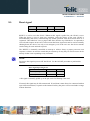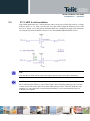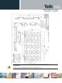
1
GL865 Hardware User Guide 1vv0300910 Rev.7 – 2014-04-02 GL865 Hardware User Guide 1vv0300910 Rev.7 – 2014-04-02 APPLICABILITY TABLE PRODUCT GL865 QUAD GL865 DUAL Reproduction forbidden without Telit Communications S.p.A. written authorization - All Rights Reserved page 2 of 76 GL865 Hardware User Guide 1vv0300910 Rev.7 – 2014-04-02 SPECIFICATIONS SUBJECT TO CHANGE WITHOUT NOTICE Notice While reasonable efforts have been made to assure the accuracy of this document, Telit assumes no liability resulting from any inaccuracies or omissions in this document, or from use of the information obtained herein. The information in this document has been carefully checked and is believed to be entirely reliable. However, no responsibility is assumed for inaccuracies or omissions. Telit reserves the right to make changes to any products described herein and reserves the right to revise this document and to make changes from time to time in content hereof with no obligation to notify any person of revisions or changes. Telit does not assume any liability arising out of the application or use of any product, software, or circuit described herein; neither does it convey license under its patent rights or the rights of others. It is possible that this publication may contain references to, or information about Telit products (machines and programs), programming, or services that are not announced in your country. Such references or information must not be construed to mean that Telit intends to announce such Telit products, programming, or services in your country. Copyrights This instruction manual and the Telit products described in this instruction manual may be, include or describe copyrighted Telit material, such as computer programs stored in semiconductor memories or other media. Laws in the Italy and other countries preserve for Telit and its licensors certain exclusive rights for copyrighted material, including the exclusive right to copy, reproduce in any form, distribute and make derivative works of the copyrighted material. Accordingly, any copyrighted material of Telit and its licensors contained herein or in the Telit products described in this instruction manual may not be copied, reproduced, distributed, merged or modified in any manner without the express written permission of Telit. Furthermore, the purchase of Telit products shall not be deemed to grant either directly or by implication, estoppel, or otherwise, any license under the copyrights, patents or patent applications of Telit, as arises by operation of law in the sale of a product. Computer Software Copyrights The Telit and 3rd Party supplied Software (SW) products described in this instruction manual may include copyrighted Telit and other 3rd Party supplied computer programs stored in semiconductor memories or other media. Laws in the Italy and other countries preserve for Telit and other 3rd Party supplied SW certain exclusive rights for copyrighted computer programs, including the exclusive right to copy or reproduce in any form the copyrighted computer program. Accordingly, any copyrighted Telit or other 3rd Party supplied SW computer programs contained in the Telit products described in this instruction manual may not be copied (reverse engineered) or reproduced in any manner without the express written permission of Telit or the 3rd Party SW supplier. Furthermore, the purchase of Telit products shall not be deemed to grant either directly or by implication, estoppel, or otherwise, any license under the copyrights, patents or patent applications of Telit or other 3rd Party supplied SW, except for the normal non-exclusive, royalty free license to use that arises by operation of law in the sale of a product. Reproduction forbidden without Telit Communications S.p.A. written authorization - All Rights Reserved page 3 of 76 GL865 Hardware User Guide 1vv0300910 Rev.7 – 2014-04-02 Usage and Disclosure Restrictions License Agreements The software described in this document is the property of Telit and its licensors. It is furnished by express license agreement only and may be used only in accordance with the terms of such an agreement. Copyrighted Materials Software and documentation are copyrighted materials. Making unauthorized copies is prohibited by law. No part of the software or documentation may be reproduced, transmitted, transcribed, stored in a retrieval system, or translated into any language or computer language, in any form or by any means, without prior written permission of Telit High Risk Materials Components, units, or third-party products used in the product described herein are NOT faulttolerant and are NOT designed, manufactured, or intended for use as on-line control equipment in the following hazardous environments requiring fail-safe controls: the operation of Nuclear Facilities, Aircraft Navigation or Aircraft Communication Systems, Air Traffic Control, Life Support, or Weapons Systems (High Risk Activities"). Telit and its supplier(s) specifically disclaim any expressed or implied warranty of fitness for such High Risk Activities. Trademarks TELIT and the Stylized T Logo are registered in Trademark Office. All other product or service names are the property of their respective owners. Copyright © Telit Communications S.p.A. 2014. Reproduction forbidden without Telit Communications S.p.A. written authorization - All Rights Reserved page 4 of 76 GL865 Hardware User Guide 1vv0300910 Rev.7 – 2014-04-02 Contents 1. INTRODUCTION........................................................................................................................................................... 7 1.1. 1.2. 1.3. 1.4. 1.5. 1.6. SCOPE ....................................................................................................................................................................... 7 AUDIENCE ................................................................................................................................................................. 7 CONTACT INFORMATION, SUPPORT........................................................................................................................... 7 DOCUMENT ORGANIZATION ..................................................................................................................................... 8 TEXT CONVENTIONS ................................................................................................................................................. 9 RELATED DOCUMENTS ............................................................................................................................................. 9 2. OVERVIEW .................................................................................................................................................................. 10 3. GL865 MECHANICAL DIMENSIONS ..................................................................................................................... 11 4. GL865 MODULE CONNECTIONS ........................................................................................................................... 12 4.1. PIN-OUT ................................................................................................................................................................ 12 4.2. ....................................................................................................................................................................................... 14 4.3. PIN LAYOUT ............................................................................................................................................................ 15 5. HARDWARE COMMANDS ....................................................................................................................................... 16 5.1. AUTO-TURNING ON THE GL865............................................................................................................................. 16 5.2. TURNING OFF THE GL865 ...................................................................................................................................... 18 5.3. RESETTING THE GL865 ........................................................................................................................................... 20 5.3.1. Hardware Unconditional restart ................................................................................................................... 20 6. POWER SUPPLY ......................................................................................................................................................... 22 6.1. POWER SUPPLY REQUIREMENTS ............................................................................................................................. 22 6.2. POWER CONSUMPTION ............................................................................................................................................ 23 6.2.1. Power consumption Plots .............................................................................................................................. 24 6.3. GENERAL DESIGN RULES ........................................................................................................................................ 28 6.3.1. Electrical Design Guidelines ......................................................................................................................... 28 6.3.2. Thermal Design Guidelines ........................................................................................................................... 31 6.3.3. Power Supply PCB layout Guidelines ........................................................................................................... 32 7. ANTENNA ..................................................................................................................................................................... 33 7.1. GSM ANTENNA REQUIREMENTS ............................................................................................................................ 33 7.1.1. GL865 Antenna – PCB line Guidelines ......................................................................................................... 33 7.2. PCB GUIDELINES IN CASE OF FCC CERTIFICATION ................................................................................................. 34 7.2.1. Transmission line design ............................................................................................................................... 35 7.2.2. Transmission line measurements ................................................................................................................... 35 7.3. GSM ANTENNA - INSTALLATION GUIDELINES ........................................................................................................ 38 8. LOGIC LEVEL SPECIFICATIONS .......................................................................................................................... 39 8.1. 9. RESET SIGNAL ......................................................................................................................................................... 40 SERIAL PORTS ........................................................................................................................................................... 41 9.1. 9.2. 9.3. 10. 10.1. MODEM SERIAL PORT ....................................................................................................................................... 41 RS232 LEVEL TRANSLATION ................................................................................................................................... 43 5V UART LEVEL TRANSLATION ............................................................................................................................. 46 AUDIO SECTION OVERVIEW ............................................................................................................................ 48 ELECTRICAL CHARACTERISTICS ............................................................................................................................. 51 Reproduction forbidden without Telit Communications S.p.A. written authorization - All Rights Reserved page 5 of 76 GL865 Hardware User Guide 1vv0300910 Rev.7 – 2014-04-02 10.1.1. 10.1.2. 11. Input Lines ..................................................................................................................................................... 51 Output Lines .................................................................................................................................................. 52 GENERAL PURPOSE I/O ...................................................................................................................................... 53 11.1. GPIO LOGIC LEVELS ............................................................................................................................................... 54 11.2. USING A GPIO PAD AS INPUT ............................................................................................................................... 55 11.3. USING A GPIO PAD AS OUTPUT ........................................................................................................................... 55 11.4. USING THE RF TRANSMISSION CONTROL GPIO4.................................................................................................... 55 11.5. USING THE RFTXMON OUTPUT GPIO5 ................................................................................................................ 55 11.6. USING THE ALARM OUTPUT GPIO6........................................................................................................................ 56 11.7. USING THE BUZZER OUTPUT GPIO7 ....................................................................................................................... 56 11.8. MAGNETIC BUZZER CONCEPTS ............................................................................................................................... 57 11.8.1. Short Description........................................................................................................................................... 57 11.8.2. Frequency Behaviour .................................................................................................................................... 57 11.8.3. Power Supply Influence ................................................................................................................................. 58 11.8.4. Working Current Influence ............................................................................................................................ 58 11.9. STAT LED INDICATION OF NETWORK SERVICE AVAILABILITY............................................................................... 59 11.10. SIMIN DETECT FUNCTION .................................................................................................................................. 60 11.11. RTC BYPASS OUT ............................................................................................................................................... 61 11.12. SIM HOLDER IMPLEMENTATION ........................................................................................................................ 61 12. DAC AND ADC SECTION ..................................................................................................................................... 62 12.1. DAC CONVERTER ................................................................................................................................................... 62 12.1.1. Description .................................................................................................................................................... 62 12.1.2. Enabling DAC ............................................................................................................................................... 63 12.1.3. Low Pass Filter Example............................................................................................................................... 63 12.2. ADC CONVERTER ................................................................................................................................................... 64 12.2.1. Description .................................................................................................................................................... 64 12.2.2. Using ADC Converter ................................................................................................................................... 64 12.3. DEBUG OF THE GL865 IN PRODUCTION ................................................................................................................... 65 13. MOUNTING THE GL865 ON YOUR BOARD .................................................................................................... 66 13.1. 13.2. 13.3. 13.4. 13.5. 13.6. 13.7. GENERAL ................................................................................................................................................................ 66 MODULE FINISHING & DIMENSIONS ........................................................................................................................ 66 RECOMMENDED FOOT PRINT FOR THE APPLICATION................................................................................................ 67 STENCIL .................................................................................................................................................................. 68 PCB PAD DESIGN .................................................................................................................................................... 68 RECOMMENDATIONS FOR PCB PAD DIMENSIONS (MM) ........................................................................................... 68 SOLDER PASTE ........................................................................................................................................................ 69 13.7.1. GL865 Solder reflow ..................................................................................................................................... 70 14. 14.1. PACKING SYSTEM ................................................................................................................................................ 71 MOISTURE SENSIBILITY ........................................................................................................................................... 73 15. CONFORMITY ASSESSMENT ISSUES .............................................................................................................. 74 16. SAFETY RECOMMANDATIONS......................................................................................................................... 75 17. DOCUMENT HISTORY ......................................................................................................................................... 76 Reproduction forbidden without Telit Communications S.p.A. written authorization - All Rights Reserved page 6 of 76 GL865 Hardware User Guide 1vv0300910 Rev.7 – 2014-04-02 1. Introduction 1.1. Scope The aim of this document is the description of some hardware solutions useful for developing a product with the Telit GL865 module. 1.2. Audience This document is intended for Telit customers, who are integrators, about to implement their applications using our GL865 modules. 1.3. Contact Information, Support For general contact, technical support, to report documentation errors and to order manuals, contact Telit’s Technical Support Center (TTSC) at: [email protected] [email protected] [email protected] [email protected] Alternatively, use: http://www.telit.com/en/products/technical-support-center/contact.php For detailed information about where you can buy the Telit modules or for recommendations on accessories and components visit: http://www.telit.com To register for product news and announcements or for product questions contact Telit’s Technical Support Center (TTSC). Our aim is to make this guide as helpful as possible. Keep us informed of your comments and suggestions for improvements. Telit appreciates feedback from the users of our information. Reproduction forbidden without Telit Communications S.p.A. written authorization - All Rights Reserved page 7 of 76 GL865 Hardware User Guide 1vv0300910 Rev.7 – 2014-04-02 1.4. Document Organization This document contains the following chapters: Chapter 1: “Introduction” provides a scope for this document, target audience, contact and support information, and text conventions. Chapter 2: “Overview” provides an overview of the document. Chapter 3: “GL865 Mechanical Dimensions” Chapter 4: “GL865 Module Connections” deals with the pin out configuration and layout. Chapter 5: “Hardware Commands” How to operate on the module via hardware. Chapter 6: “Power supply” Power supply requirements and general design rules. Chapter 7: “Antenna” The antenna connection and board layout design are the most important parts in the full product design. Chapter 8: “Logic Level specifications” Specific values adopted in the implementation of logic levels for this module. Chapter 9: “Serial ports” The serial port on the Telit GL865 is the core of the interface between the module and OEM hardware Chapter 10: “Audio Section overview” Refers to the audio blocks of the Base Band Chip of the GL865 Telit Modules. Chapter 11: “General Purpose I/O” How the general purpose I/O pads can be configured. Chapter 12 “DAC and ADC Section” Deals with these two kind of converters. Chapter 13: “Mounting the GL865 on the application board” Recommendations and specifics on how to mount the module on the user’s board. Reproduction forbidden without Telit Communications S.p.A. written authorization - All Rights Reserved page 8 of 76 GL865 Hardware User Guide 1vv0300910 Rev.7 – 2014-04-02 1.5. Text Conventions Danger – This information MUST be followed or catastrophic equipment failure or bodily injury may occur. Caution or Warning – Alerts the user to important points about integrating the module, if these points are not followed, the module and end user equipment may fail or malfunction. Tip or Information – Provides advice and suggestions that may be useful when integrating the module. All dates are in ISO 8601 format, i.e. YYYY-MM-DD. 1.6. Related Documents • Telit's GSM/GPRS Family Software User Guide, 1vv0300784 • Audio settings application note , 80000NT10007a • Digital Voice Interface Application Note, 80000NT10004a • GL865 Product description, 80370ST10080a • SIM Holder Design Guides, 80000NT10001a • AT Commands Reference Guide, 80000ST10025a • Telit EVK2 User Guide, 1vv0300704 Reproduction forbidden without Telit Communications S.p.A. written authorization - All Rights Reserved page 9 of 76 GL865 Hardware User Guide 1vv0300910 Rev.7 – 2014-04-02 2. Overview The aim of this document is the description of some hardware solutions useful for developing a product with the Telit GL865 module. In this document all the basic functions of a mobile phone will be taken into account; for each one of them a proper hardware solution will be suggested and eventually the wrong solutions and common errors to be avoided will be evidenced. Obviously this document cannot embrace the whole hardware solutions and products that may be designed. The wrong solutions to be avoided shall be considered as mandatory, while the suggested hardware configurations shall not be considered mandatory, instead the information given shall be used as a guide and a starting point for properly developing your product with the Telit GL865 module. For further hardware details that may not be explained in this document refer to the Telit GL865 Product Description document where all the hardware information is reported. NOTICE: The integration of the GSM/GPRS GL865 cellular module within user application shall be done according to the design rules described in this manual. The information presented in this document is believed to be accurate and reliable. However, no responsibility is assumed by Telit Communications S.p.A. for its use, nor any infringement of patents or other rights of third parties which may result from its use. No license is granted by implication or otherwise under any patent rights of Telit Communications S.p.A. other than for circuitry embodied in Telit products. This document is subject to change without notice. Reproduction forbidden without Telit Communications S.p.A. written authorization - All Rights Reserved page 10 of 76 GL865 Hardware User Guide 1vv0300910 Rev.7 – 2014-04-02 3. GL865 Mechanical Dimensions The GL865 overall dimensions are: • • • • Length: Width: Thickness: Weight 24.4 mm 24.4 mm 2.7 mm 2.48 g Reproduction forbidden without Telit Communications S.p.A. written authorization - All Rights Reserved page 11 of 76 GL865 Hardware User Guide 1vv0300910 Rev.7 – 2014-04-02 4. GL865 module connections 4.1. PIN-OUT Pad Signal I/O Function Note Type Audio 20 EAR- AO Earphone signal output, phase - Audio 21 EAR+ AO Earphone signal output, phase + Audio 22 MIC- AI Mic.signal input; phase- Audio 24 MIC+ AI Mic.signal input; phase+ Audio 23 AGND - Analog Ground - SIM card interface 9 SIMVCC - External SIM signal – Power supply for the SIM 1,8 / 3V 10 SIMRST O External SIM signal – Reset 1,8 / 3V 11 SIMCLK O External SIM signal – Clock 1,8 / 3V 4.7K Pull up 12 SIMIO I/O External SIM signal – Data I/O X All GPI0 can be program med SIMIN I Presence SIM input (See para 11.9) 44 RX_AUX I Auxiliary UART (RX Data) CMOS 2.8V 45 TX_AUX O Auxiliary UART (TX Data) CMOS 2.8V 1,8 / 3V CMOS 2.8V Trace 7 C103/TXD I Prog. / Data + HW Flow Control Output for Data carrier detect signal (DCD) to DTE / GP output Output for Ring indicator signal (RI) to DTE / GP output Output for Data set ready signal (DSR) to DTE / GP output Input for Data terminal ready signal (DTR) from DTE / GP input Input for Request to send signal (RTS) from DTE / GP input Output for Clear to send signal (CTS) to DTE / GP output Serial data input (TXD) from DTE 8 C104/RXD O Serial data output to DTE 1 C109/DCD/GPO O 2 C125/RING/GPO O 3 C107/DSR/GPO O 4 C108/DTR/GPI I 5 C105/RTS/GPI I 6 C106/CTS/GPO O CMOS 2.8V CMOS 2.8V CMOS 2.8V CMOS 2.8V CMOS 2.8V CMOS 2.8V CMOS 2.8V CMOS 2.8V DAC and ADC 13 ADC_IN1 AI Analog/Digital converter input A/D 14 ADC_IN2 AI Analog/Digital converter input A/D 15 DAC_OUT AO Digital/Analog converter output D/A 30 VRTC AO VRTC Backup Power 47 RESET* I CMOS 1.8V 43 V_AUX / PWRMON O Reset input 2.8V stabilized output Imax=100mA / Power ON monitor Miscellaneous Functions Reproduction forbidden without Telit Communications S.p.A. written authorization - All Rights Reserved Power Out 2.8V page 12 of 76 GL865 Hardware User Guide 1vv0300910 Rev.7 – 2014-04-02 Pad Signal I/O Function 34 Antenna O Antenna output – 50 Ω GPIO GPIO01 Configurable GPIO / Digital Audio Interface (WA0) GPIO02 Configurable GPIO / Jammer Detect Report / Digital Audio Interface (RX) GPIO03 Configurable GPIO / Digital Audio Interface (TX) GPIO04 Configurable GPIO / TX Disable input / Digital Audio Interface (CLK) GPIO05 Configurable GPIO / Transmitter ON monitor GPIO06 Configurable GPIO / ALARM GPIO07 Configurable GPIO / Buzzer GPIO08 Configurable GPIO / STAT LED Power Supply Note Type RF 42 GPIO_01 / DVI_WA0 I/O 41 GPIO_02 / JDR / DVI_RX I/O 40 GPIO_03 / DVI_TX I/O 39 GPIO_04 / TX Disable / DVI_CLK I/O 29 GPIO_05 / RFTXMON I/O 28 GPIO_06 / ALARM I/O 27 GPIO_07 / BUZZER I/O 26 GPIO_08 / STAT_LED I/O 38 VBATT - Main power supply (Baseband) Power 37 VBATT_PA - Main power supply (Radio PA) Power 23 AGND - AF Signal Ground (see audio section) AF Signal 32 GND - Ground Power 33 GND - Ground Power 35 GND - Ground Power 36 GND - Ground Power 46 GND - Ground Power CMOS 2.8V CMOS 2.8V CMOS 2.8V CMOS 2.8V CMOS 2.8V CMOS 2.8V CMOS 2.8V CMOS 2.8V RESERVED 48 - 16 - 17 - 18 - 19 - 25 - 31 - WARNING: Reserved pins must not be connected. Reproduction forbidden without Telit Communications S.p.A. written authorization - All Rights Reserved page 13 of 76 GL865 Hardware User Guide 1vv0300910 Rev.7 – 2014-04-02 NOTE: If not used, almost all pins should be left disconnected. The only exceptions are the following pins: 4.2. pin 38, 37 32, 33, 35, 36, 46 23 7 8 5 43 signal VBATT & VBATT_PA GND AGND TXD RXD RTS 47 45 44 RESET* TX_AUX RX_AUX V_AUX / PWRMON Reproduction forbidden without Telit Communications S.p.A. written authorization - All Rights Reserved page 14 of 76 GL865 Hardware User Guide 1vv0300910 Rev.7 – 2014-04-02 4.3. Pin Layout TOP VIEW NOTE: The pin defined as NC/RFU has to be considered RESERVED and don’t connect on any pin in the application. Reproduction forbidden without Telit Communications S.p.A. written authorization - All Rights Reserved page 15 of 76 GL865 Hardware User Guide 1vv0300910 Rev.7 – 2014-04-02 5. Hardware Commands 5.1. Auto-Turning ON the GL865 To Auto-turn on the GL865, the power supply must be applied on the power pins VBATT and VBATT_PA, after 1000 m-seconds, the V_AUX / PWRMON pin will be at the high logic level and the module can be consider fully operating. When the power supply voltage is lower than 3.4V, after 5000 m-seconds, the V_AUX / PWRMON pin will be at the high logic level and the module can be consider fully operating. The following flow chart shows the proper turn on procedure: Modem ON Proc. PWR supply = ON? N Y PWMON = ON? Y Delay 300mS Enter AT<CR> AT answer in 1second ? N Delay 1s - 5s for Low Voltage Operating PWMON = ON? Y AT init sequence. N N Modem Reset Proc. Y Delay 1s Start AT CMD. Reproduction forbidden without Telit Communications S.p.A. written authorization - All Rights Reserved page 16 of 76 GL865 Hardware User Guide 1vv0300910 Rev.7 – 2014-04-02 NOTE: The power supply on the pins VBATT and VBATT_PA must be applied at the same time or for the special application in the first apply the VBATT_PA and in second time apply VBATT, never vice versa in this case can be damage the unit. NOTE: In order to avoid a back powering effect it is recommended to avoid having any HIGH logic level signal applied to the digital pins of the GL865 when the module is powered OFF or during an ON/OFF transition. A flow chart showing the AT command managing procedure is displayed below: Start AT CMD. Delay 300mS Enter AT<CR> AT answer in 1second ? Y AT init sequence. N Disconnect PWR supply Modem ON Proc. Reproduction forbidden without Telit Communications S.p.A. written authorization - All Rights Reserved page 17 of 76 GL865 Hardware User Guide 1vv0300910 Rev.7 – 2014-04-02 5.2. Turning OFF the GL865 Turning off of the device can be done in two ways: • General turn OFF • Processor turn OFF General turn OFF – disconnect the power supply from the both power pins VBATT and VBATT_PA at the same time. In this case all parts of the module are in OFF condition, any power consumption is present. Processor turn OFF – disconnect the power supply only from the power pin VBATT, the power pin VBATT_PA can be connected to power supply, in this case a low, typical 2uA max 20uA, power consumption is present. Before any of both OFF procedure will be applied, the AT#SYSHALT AT command must be send (see AT Commands Reference Guide, 80000ST10025a), after the OK response message, check the V_AUX / PWRMON pin, when the logic level is low the module can be consider fully not operating and at this moment is possible disconnect the Power Supply. The following flow chart shows the proper turnoff procedure: Reproduction forbidden without Telit Communications S.p.A. written authorization - All Rights Reserved page 18 of 76 GL865 Hardware User Guide 1vv0300910 Rev.7 – 2014-04-02 Modem OFF Proc. PWRMON = OFF? Y Disconnect PWR supply N Place AT command AT#SYSHALT Wait PWRMON =OFF or 15s timeout Disconnect PWR supply Delay 1.5s Modem ON Proc. TIP: To check if the device has been powered off, the hardware line PWRMON must be monitored. The device is powered off when PWRMON goes low. NOTE: In order to avoid a back powering effect it is recommended to avoid having any HIGH logic level signal applied to the digital pins of the GL865 when the module is powered OFF or during an ON/OFF transition. Reproduction forbidden without Telit Communications S.p.A. written authorization - All Rights Reserved page 19 of 76 GL865 Hardware User Guide 1vv0300910 Rev.7 – 2014-04-02 5.3. Resetting the GL865 5.3.1. Hardware Unconditional restart WARNING: The hardware unconditional Restart must not be used during normal operation of the device since it does not detach the device from the network. It shall be kept as an emergency exit procedure to be done in the rare case that the device gets stacked waiting for some network or SIM responses. To unconditionally reboot the GL865, the pad RESET* must be tied low for at least 200 milliseconds and then released. NOTE: Do not use any pull up resistor on the RESET* line nor any totem pole digital output. Using pull up resistor may bring to latch up problems on the GL865 power regulator and improper functioning of the module. The line RESET* must be connected only in open collector configuration; the transistor must be connected as close as possible to the RESET* pin. TIP: The unconditional hardware restart must always be implemented on the boards and the software must use it as an emergency exit procedure. A simple circuit to do it is: Reproduction forbidden without Telit Communications S.p.A. written authorization - All Rights Reserved page 20 of 76 GL865 Hardware User Guide 1vv0300910 Rev.7 – 2014-04-02 In the following flow chart is detailed the proper restart procedure: Modem Reset Proc. Reset = LOW Delay 200ms Reset = HIGH PWRMON = OFF Y Delay 1,5s Disconnect PWR supply Modem ON Proc. N Delay 1s Start AT CMD. NOTE: In order to avoid a back powering effect it is recommended to avoid having any HIGH logic level signal applied to the digital pins of the GL865 when the module is powered OFF or during an ON/OFF transition. Reproduction forbidden without Telit Communications S.p.A. written authorization - All Rights Reserved page 21 of 76 GL865 Hardware User Guide 1vv0300910 Rev.7 – 2014-04-02 6. Power Supply The power supply circuitry and board layout are a very important part in the full product design and they strongly reflect on the product overall performances, hence read carefully the requirements and the guidelines that will follow for a proper design. 6.1. Power Supply Requirements The external power supply must be connected to VBATT & VBATT_PA signals and must fulfill the following requirements: POWER SUPPLY Nominal Supply Voltage Normal Operating Voltage Range Extended Operating Voltage Range 3.8 V 3.4 V÷ 4.20 V 3.22 V÷ 4.50 V NOTE: The Operating Voltage Range MUST never be exceeded; care must be taken in order to fulfil min/max voltage requirement. NOTE: Overshoot voltage (regarding MAX Extended Operating Voltage) and drop in voltage (regarding MIN Extended Operating Voltage) MUST never be exceeded; The “Extended Operating Voltage Range” can be used only with completely assumption and application of the HW User guide suggestions. NOTE: When the power supply voltage is lower than 3.4V, after 4000 m-seconds, the V_AUX / PWRMON pin will be at the high logic level and the module can be consider fully operating. See para 5.1. Reproduction forbidden without Telit Communications S.p.A. written authorization - All Rights Reserved page 22 of 76 GL865 Hardware User Guide 1vv0300910 Rev.7 – 2014-04-02 6.2. Power Consumption The GL865 power consumptions are: Mode SWITCHED OFF Switched Off Average (mA) Typical 2uA max 20uA Switched Off with <650uA AT#SYSHALT IDLE mode AT+CFUN=1 21,0 AT+CFUN=4 18,0 3,9 2,5 AT+CFUN=0 or =5 2,4 1,5 CSD TX and RX mode GSM900 CSD PL5 230 DCS1800 CSD PL0 175 GPRS (class 1) 1TX + 1RX GSM900 PL5 225 DCS1800 PL0 160 GPRS (class 10) 2TX + 3RX GSM900 PL5 360 DCS1800 PL0 290 GL 865 Mode description Module power supplied only on VBATT_PA pin, the VBATT pin is not power supplied. Module power supplied on VBATT_PA pin and VBATT pin, the at command AT#SYSHALT is applied. Normal mode: full functionality of the module Disabled TX and RX; module is not registered on the network Paging Multiframe 2 Paging Multiframe 3 Paging Multiframe 4 Paging Multiframe 9 GSM Voice call GPRS Sending data mode GPRS Sending data mode The GSM system is made in a way that the RF transmission is not continuous, else it is packed into bursts at a base frequency of about 216 Hz, and the relative current peaks can be as high as about 2A. Therefore the power supply has to be designed in order to withstand with these current peaks without big voltage drops; this means that both the electrical design and the board layout must be designed for this current flow. If the layout of the PCB is not well designed a strong noise floor is generated on the ground and the supply; this will reflect on all the audio paths producing an audible annoying noise at 216 Hz; if the voltage drop during the peak current absorption is too much, then the device may even shutdown as a consequence of the supply voltage drop. NOTE: The electrical design for the Power supply should be made ensuring it will be capable of a peak current output of at least 2 A. Reproduction forbidden without Telit Communications S.p.A. written authorization - All Rights Reserved page 23 of 76 GL865 Hardware User Guide 1vv0300910 Rev.7 – 2014-04-02 6.2.1. Power consumption Plots This document section is showing the typical Current consumption plots (using Agilent 66319D) in the normal working conditions of the module. GSM900 – Voice Call – Power level 5 Reproduction forbidden without Telit Communications S.p.A. written authorization - All Rights Reserved page 24 of 76 GL865 Hardware User Guide 1vv0300910 Rev.7 – 2014-04-02 GSM900 – GPRS Call – Power level 5 - 1 Slot TX GSM900 – GPRS Call – Power level 5 - 2 Slot TX, 3 Slot RX Reproduction forbidden without Telit Communications S.p.A. written authorization - All Rights Reserved page 25 of 76 GL865 Hardware User Guide 1vv0300910 Rev.7 – 2014-04-02 DCS1800 – Voice Call – Power level 0 DCS1800 – GPRS Call – Power level 0 – 1 Slot TX Reproduction forbidden without Telit Communications S.p.A. written authorization - All Rights Reserved page 26 of 76 GL865 Hardware User Guide 1vv0300910 Rev.7 – 2014-04-02 PCS1900 – GPRS Call – Power level 0 - 2 Slot TX, 3 Slot RX Reproduction forbidden without Telit Communications S.p.A. written authorization - All Rights Reserved page 27 of 76 GL865 Hardware User Guide 1vv0300910 Rev.7 – 2014-04-02 6.3. General Design Rules The principal guidelines for the Power Supply Design embrace three different design steps: • the electrical design • the thermal design • the PCB layout. 6.3.1. Electrical Design Guidelines The electrical design of the power supply depends strongly from the power source where this power is drained. We will distinguish them into three categories: • +5V input (typically PC internal regulator output) • +12V input (typically automotive) • Battery 6.3.1.1. + 5V input Source Power Supply Design Guidelines The desired output for the power supply is 3.8V, hence there's not a big difference between the input source and the desired output and a linear regulator can be used. A switching power supply will not be suited because of the low drop out requirements. When using a linear regulator, a proper heat sink shall be provided in order to dissipate the power generated. A Bypass low ESR capacitor of adequate capacity must be provided in order to cut the current absorption peaks close to the GL865, a 100μF tantalum capacitor is usually suited. Make sure the low ESR capacitor on the power supply output (usually a tantalum one) is rated at least 10V. A protection diode should be inserted close to the power input, in order to save the GL865 from power polarity inversion. An example of linear regulator with 5V input is: Reproduction forbidden without Telit Communications S.p.A. written authorization - All Rights Reserved page 28 of 76 GL865 Hardware User Guide 1vv0300910 Rev.7 – 2014-04-02 6.3.1.2. + 12V input Source Power Supply Design Guidelines The desired output for the power supply is 3.8V, hence due to the big difference between the input source and the desired output, a linear regulator is not suited and shall not be used. A switching power supply will be preferable because of its better efficiency especially with the 2A peak current load represented by the GL865. When using a switching regulator, a 500kHz or more switching frequency regulator is preferable because of its smaller inductor size and its faster transient response. This allows the regulator to respond quickly to the current peaks absorption. In any case the frequency and Switching design selection is related to the application to be developed due to the fact the switching frequency could also generate EMC interferences. For car PB battery the input voltage can rise up to 15,8V and this should be kept in mind when choosing components: all components in the power supply must withstand this voltage. A Bypass low ESR capacitor of adequate capacity must be provided in order to cut the current absorption peaks, a 100μF tantalum capacitor is usually suited. Make sure the low ESR capacitor on the power supply output (usually a tantalum one) is rated at least 10V. For Car applications a spike protection diode should be inserted close to the power input, in order to clean the supply from spikes. A protection diode should be inserted close to the power input, in order to save the GL865 from power polarity inversion. This can be the same diode as for spike protection. An example of switching regulator with 12V input is in the below schematic (split in 2 parts): Reproduction forbidden without Telit Communications S.p.A. written authorization - All Rights Reserved page 29 of 76 GL865 Hardware User Guide 1vv0300910 Rev.7 – 2014-04-02 6.3.1.3. Battery Source Power Supply Design Guidelines The desired nominal output for the power supply is 3.8V and the maximum voltage allowed is 4.2V, hence a single 3.7V Li-Ion cell battery type is suited for supplying the power to the Telit GL865 module. WARNING: The three cells Ni/Cd or Ni/MH 3,6 V Nom. battery types or 4V PB types MUST NOT BE USED DIRECTLY since their maximum voltage can rise over the absolute maximum voltage for the GL865 and damage it. NOTE: DON'T USE any Ni-Cd, Ni-MH, and Pb battery types directly connected with GL865. Their use can lead to overvoltage on the GL865 and damage it. USE ONLY Li-Ion battery types. A Bypass low ESR capacitor of adequate capacity must be provided in order to cut the current absorption peaks, a 100μF tantalum capacitor is usually suited. Make sure the low ESR capacitor (usually a tantalum one) is rated at least 10V. A protection diode should be inserted close to the power input, in order to save the GL865 from power polarity inversion. Otherwise the battery connector should be done in a way to avoid polarity inversions when connecting the battery. The battery capacity must be at least 500mAh in order to withstand the current peaks of 2A; the suggested capacity is from 500mAh to 1000mAh. Reproduction forbidden without Telit Communications S.p.A. written authorization - All Rights Reserved page 30 of 76 GL865 Hardware User Guide 1vv0300910 Rev.7 – 2014-04-02 6.3.2. Thermal Design Guidelines The thermal design for the power supply heat sink should be done with the following specifications: See para 7.2 Power Consumption NOTE: The average consumption during transmissions depends on the power level at which the device is requested to transmit by the network. The average current consumption hence varies significantly. Considering the very low current during idle, especially if Power Saving function is enabled, it is possible to consider from the thermal point of view that the device absorbs current significantly only during calls. For the heat generated by the GL865, you can consider it to be during transmission 1W max during CSD/VOICE calls and 2W max during class10 GPRS upload. This generated heat will be mostly conducted to the ground plane under the GL865; you must ensure that your application can dissipate it. Reproduction forbidden without Telit Communications S.p.A. written authorization - All Rights Reserved page 31 of 76 GL865 Hardware User Guide 1vv0300910 Rev.7 – 2014-04-02 6.3.3. Power Supply PCB layout Guidelines As seen on the electrical design guidelines the power supply shall have a low ESR capacitor on the output to cut the current peaks and a protection diode on the input to protect the supply from spikes and polarity inversion. The placement of these components is crucial for the correct working of the circuitry. A misplaced component can be useless or can even decrease the power supply performances. The Bypass low ESR capacitor must be placed close to the Telit GL865 power input pads or in the case the power supply is a switching type it can be placed close to the inductor to cut the ripple provided the PCB trace from the capacitor to the GL865 is wide enough to ensure a dropless connection even during the 2A current peaks. The protection diode must be placed close to the input connector where the power source is drained. The PCB traces from the input connector to the power regulator IC must be wide enough to ensure no voltage drops occur when the 2A current peaks are absorbed. Note that this is not made in order to save power loss but especially to avoid the voltage drops on the power line at the current peaks frequency of 216 Hz that will reflect on all the components connected to that supply, introducing the noise floor at the burst base frequency. For this reason while a voltage drop of 300-400 mV may be acceptable from the power loss point of view, the same voltage drop may not be acceptable from the noise point of view. If your application doesn't have audio interface but only uses the data feature of the Telit GL865, then this noise is not so disturbing and power supply layout design can be more forgiving. The PCB traces to the GL865 and the Bypass capacitor must be wide enough to ensure no significant voltage drops occur when the 2A current peaks are absorbed. This is for the same reason as previous point. Try to keep this trace as short as possible. The PCB traces connecting the Switching output to the inductor and the switching diode must be kept as short as possible by placing the inductor and the diode very close to the power switching IC (only for switching power supply). This is done in order to reduce the radiated field (noise) at the switching frequency (100-500 kHz usually). The use of a good common ground plane is suggested. The placement of the power supply on the board should be done in such a way to guarantee that the high current return paths in the ground plane are not overlapped to any noise sensitive circuitry as the microphone amplifier/buffer or earphone amplifier. The power supply input cables should be kept separate from noise sensitive lines such as microphone/earphone cables. Reproduction forbidden without Telit Communications S.p.A. written authorization - All Rights Reserved page 32 of 76 GL865 Hardware User Guide 1vv0300910 Rev.7 – 2014-04-02 7. Antenna The antenna connection and board layout design are the most important aspect in the full product design as they strongly affect the product overall performances, hence read carefully and follow the requirements and the guidelines for a proper design. 7.1. GSM Antenna Requirements As suggested on the Product Description the antenna and antenna transmission line on PCB for a Telit GL865 device shall fulfil the following requirements: ANTENNA REQUIREMENTS Frequency range Gain Impedance Input power VSWR absolute max VSWR recommended QUAD 824-894 MHz GSM850 band 880-960 MHz GSM900 band 1710-1885MHz DCS1800 band 1850-1990MHz PCS1900 band 1.4dBi @ GSM900 and 3dBi @ DCS1800 1.4dBi @ GSM850 and 3dBi @ PCS1900 50 Ohm >2W ≤ 10:1 (limit to avoid permanent damage) ≤ 2:1 (limit to fulfil all regulatory requirements) DUAL 880-960 MHz GSM900 band 1710-1885MHz MHz DCS1800 band 1.4dBi @ GSM900 and 3dBi @ DCS1800 50 Ohm >2W ≤ 10:1 (limit to avoid permanent damage) ≤ 2:1 (limit to fulfil all regulatory requirements) Furthermore if the devices are developed for the US market and/or Canada market, they shall comply to the FCC and/or IC approval requirements: Those devices are to be used only for mobile and fixed application. The antenna(s) used for this transmitter must be installed to provide a separation distance of at least 20 cm from all persons and must not be co-located or operating in conjunction with any other antenna or transmitter. End-Users must be provided with transmitter operation conditions for satisfying RF exposure compliance. OEM integrators must ensure that the end user has no manual instructions to remove or install the GL865. Antennas used for those OEM modules must not exceed 3dBi gain for mobile and fixed operating configurations. 7.1.1. GL865 Antenna – PCB line Guidelines When using the Telit GL865 module, since there's no antenna connector on the module, the antenna must be connected to the GL865 through the PCB with the antenna pad (pin 34). In the case that the antenna is not directly developed on the same PCB, hence directly connected at the antenna pad of the GL865, then a PCB line is needed in order to connect with it or with its connector. Reproduction forbidden without Telit Communications S.p.A. written authorization - All Rights Reserved page 33 of 76 GL865 Hardware User Guide 1vv0300910 Rev.7 – 2014-04-02 This line of transmission shall fulfill the following requirements: ANTENNA LINE ON PCB REQUIREMENTS 50 ohm Impedance 0,3 dB Max Attenuation No coupling with other signals allowed Cold End (Ground Plane) of antenna shall be equipotential to the GL865 ground pins This transmission line should be designed according to the following guidelines: • • • • • • • • • • 7.2. Ensure that the antenna line impedance is 50 ohm; Keep the antenna line on the PCB as short as possible, since the antenna line loss shall be less than 0,3 dB; Antenna line must have uniform characteristics, constant cross section, avoid meanders and abrupt curves; Keep, if possible, one layer of the PCB used only for the Ground plane; Surround (on the sides, over and under) the antenna line on PCB with Ground, avoid having other signal tracks facing directly the antenna line track; The ground around the antenna line on PCB has to be strictly connected to the Ground Plane by placing vias once per 2mm at least; Place EM noisy devices as far as possible from GL865 antenna line; Keep the antenna line far away from the GL865 power supply lines; If you have EM noisy devices around the PCB hosting the GL865, such as fast switching ICs, take care of the shielding of the antenna line by burying it inside the layers of PCB and surround it with Ground planes, or shield it with a metal frame cover. If you don't have EM noisy devices around the PCB of GL865, by using a strip-line on the superficial copper layer for the antenna line, the line attenuation will be lower than a buried one; PCB Guidelines in case of FCC certification In the case FCC certification is required for an application using GL865, according to FCC KDB 996369 for modular approval requirements, the transmission line has to be similar to that implemented on GL865 interface board and described in the following chapter. Reproduction forbidden without Telit Communications S.p.A. written authorization - All Rights Reserved page 34 of 76 GL865 Hardware User Guide 1vv0300910 Rev.7 – 2014-04-02 7.2.1. Transmission line design During the design of the GL865 interface board, the placement of components has been chosen properly, in order to keep the line length as short as possible, thus leading to lowest power losses possible. A Grounded Coplanar Waveguide (G-CPW) line has been chosen, since this kind of transmission line ensures good impedance control and can be implemented in an outer PCB layer as needed in this case. A SMA female connector has been used to feed the line. The interface board is realized on a FR4, 4-layers PCB. Substrate material is characterized by relative permittivity εr = 4.6 ± 0.4 @ 1 GHz, TanD= 0.019 ÷ 0.026 @ 1 GHz. A characteristic impedance of nearly 50 Ω is achieved using trace width = 1.1 mm, clearance from coplanar ground plane = 0.3 mm each side. The line uses reference ground plane on layer 3, while copper is removed from layer 2 underneath the line. Height of trace above ground plane is 1.335 mm. Calculated characteristic impedance is 51.6 Ω, estimated line loss is less than 0.1 dB. The line geometry is shown below: 7.2.2. 0.3 mm 0.2 mm 6. 2 0.035 mm 0.3 mm L1 1.1 mm FR4 1.335 mm L2 0.035 mm 0.035 mm m m 1.1 mm L3 Transmission line measurements HP8753E VNA (Full-2-port calibration) has been used in this measurement session. A calibrated coaxial cable has been soldered at the pad corresponding to GL865 RF output; a SMA connector has been soldered to the board in order to characterize the losses of the transmission line including the connector itself. During Return Loss / impedance measurements, the transmission line has been terminated to 50 Ω load. Reproduction forbidden without Telit Communications S.p.A. written authorization - All Rights Reserved page 35 of 76 GL865 Hardware User Guide 1vv0300910 Rev.7 – 2014-04-02 Return Loss plot of line under test is shown below: Reproduction forbidden without Telit Communications S.p.A. written authorization - All Rights Reserved page 36 of 76 GL865 Hardware User Guide 1vv0300910 Rev.7 – 2014-04-02 Line input impedance (in Smith Chart format, once the line has been terminated to 50 Ω load) is shown in the following figure: Insertion Loss of G-CPW line plus SMA connector is shown below: Reproduction forbidden without Telit Communications S.p.A. written authorization - All Rights Reserved page 37 of 76 GL865 Hardware User Guide 1vv0300910 Rev.7 – 2014-04-02 7.3. GSM Antenna - Installation Guidelines • Install the antenna in a place covered by the GSM signal. • The Antenna must be installed to provide a separation distance of at least 20 cm from all persons and must not be co-located or operating in conjunction with any other antenna or transmitter; • Antenna shall not be installed inside metal cases • Antenna shall be installed also according Antenna manufacturer instructions. Reproduction forbidden without Telit Communications S.p.A. written authorization - All Rights Reserved page 38 of 76 GL865 Hardware User Guide 1vv0300910 Rev.7 – 2014-04-02 8. Logic level specifications Where not specifically stated, all the interface circuits work at 2.8V CMOS logic levels. The following table shows the logic level specifications used in the GL865 interface circuits: Absolute Maximum Ratings -Not Functional Parameter Min Max Input level on any digital pin (CMOS 2.8) when on Input level on any digital pin (CMOS 1.8) when on Input voltage on analog pins when on -0.3V +3.1V -0.3V +2.1V -0.3V +3.0 V Operating Range - Interface levels (2.8V CMOS) Level Min Max Input high level 2.1V 3.1V Input low level 0V 0.5V Output high level 2.2V 3.1V Output low level 0V 0.35V For 1.8V signals: Operating Range - Interface levels (1.8V CMOS) Level Min Max Input high level 1.6V 2.0V Input low level 0V 0.4V Output high level 1,65V 2.0V Output low level 0V 0.35V Current characteristics Level Typical Output Current 1mA Input Current 1uA Reproduction forbidden without Telit Communications S.p.A. written authorization - All Rights Reserved page 39 of 76 GL865 Hardware User Guide 1vv0300910 Rev.7 – 2014-04-02 8.1. Reset signal Signal Function I/O pin RESET* Phone reset I 47 RESET* is used to reset the GL865. Whenever this signal is pulled low, the GL865 is reset. When the device is reset it stops any operation. After the release of the reset GL865 is unconditionally shut down, without doing any detach operation from the network where it is registered. This behaviour is not a proper shut down because any GSM device is requested to issue a detach request on turn off. For this reason the Reset signal must not be used to normally shutting down the device, but only as an emergency exit in the rare case the device remains stuck waiting for some network response. The RESET* is internally controlled on start-up to achieve always a proper power-on reset sequence, so there's no need to control this pin on start-up. It may only be used to reset a device already on that is not responding to any command. NOTE: Do not use this signal to power OFF the GL865. Use the ON/OFF procedure to perform this function. Reset Signal Operating levels: Signal Min Max RESET* Input high 1.8V(NOTE1) 2.1V RESET* Input low 0V 0.2V * this signal is internally pulled up so the pin can be left floating if not used. If unused, this signal may be left unconnected. If used, then it must always be connected with an open collector transistor, to permit to the internal circuitry the power on reset and under voltage lockout functions. Reproduction forbidden without Telit Communications S.p.A. written authorization - All Rights Reserved page 40 of 76 GL865 Hardware User Guide 1vv0300910 Rev.7 – 2014-04-02 9. Serial Ports The serial port on the GL865 is the core of the interface between the module and OEM hardware. 2 serial ports are available on the module: MODEM SERIAL PORT 1 (MAIN) for AT commands and Data MODEM SERIAL PORT 2 (AUX) for AT commands or Debug 9.1. MODEM SERIAL PORT Several configurations can be designed for the serial port on the OEM hardware, but the most common are: RS232 PC com port microcontroller UART @ 2.8V - 3V (Universal Asynchronous Receive Transmit) microcontroller UART @ 5V or other voltages different from 2.8V Depending from the type of serial port on the OEM hardware a level translator circuit may be needed to make the system work. The only configuration that doesn't need a level translation is the 2.8V UART. The serial port on the GL865 is a +2.8V UART with all the 7 RS232 signals. It differs from the PC-RS232 in the signal polarity (RS232 is reversed) and levels. The levels for the GL865 UART are the CMOS levels: Absolute Maximum Ratings -Not Functional Parameter Min Max Input level on any digital pad when on Input voltage on analog pads when on -0.3V +3.1V -0.3V +3.1V Operating Range - Interface levels (2.8V CMOS) Level Min Max Input high level VIH 2.1V 3.1 V Input low level VIL 0V 0.5V Output high level VOH 2.2V Output low level VOL 0V Reproduction forbidden without Telit Communications S.p.A. written authorization - All Rights Reserved page 41 of 76 GL865 Hardware User Guide 1vv0300910 Rev.7 – 2014-04-02 The signals of the GL865 serial port are: RS232 Pin Number Signal GL865 Pad Number Name 1 DCD - dcd_uart 1 Data Carrier Detect 2 3 RXD - tx_uart TXD - rx_uart 8 7 Transmit line *see Note Receive line *see Note 4 DTR - dtr_uart 4 Data Terminal Ready 5 GND 32, 33, 35, 36, 46 Ground 6 DSR - dsr_uart 3 Data Set Ready 7 RTS -rts_uart 5 Request to Send 8 CTS - cts_uart 6 Clear to Send 9 RI - ri_uart 2 Ring Indicator Usage Output from the GL865 that indicates the carrier presence Output transmit line of GL865 UART Input receive of the GL865 UART Input to the GL865 that controls the DTE READY condition ground Output from the GL865 that indicates the module is ready Input to the GL865 that controls the Hardware flow control Output from the GL865 that controls the Hardware flow control Output from the GL865 that indicates the incoming call condition NOTE: According to V.24, RX/TX signal names are referred to the application side, therefore on the GL865 side these signal are on the opposite direction: TXD on the application side will be connected to the receive line (here named TXD/ rx_uart ) of the GL865 serial port and viceversa for RX. NOTE: For a minimum implementation, only the TXD and RXD lines can be connected, the other lines can be left open provided a software flow control is implemented. NOTE: In order to avoid a back powering effect it is recommended to avoid having any HIGH logic level signal applied to the digital pins of the GL865 when the module is powered off or during an ON/OFF transition. Reproduction forbidden without Telit Communications S.p.A. written authorization - All Rights Reserved page 42 of 76 GL865 Hardware User Guide 1vv0300910 Rev.7 – 2014-04-02 9.2. RS232 level translation In order to interface the GL865 with a PC com port or a RS232 (EIA/TIA-232) application a level translator is required. This level translator must: • invert the electrical signal in both directions; • change the level from 0/2.8V to +15/-15V . Actually, the RS232 UART 16450, 16550, 16650 & 16750 chipsets accept signals with lower levels on the RS232 side (EIA/TIA-562), allowing a lower voltage-multiplying ratio on the level translator. Note that the negative signal voltage must be less than 0V and hence some sort of level translation is always required. The simplest way to translate the levels and invert the signal is by using a single chip level translator. There are a multitude of them, differing in the number of drivers and receivers and in the levels (be sure to get a true RS232 level translator not a RS485 or other standards). By convention the driver is the level translator from the 0-2.8V UART to the RS232 level. The receiver is the translator from the RS232 level to 0-2.8V UART. In order to translate the whole set of control lines of the UART you will need: • 5 drivers • 3 receivers NOTE: The digital input lines working at 2.8V CMOS have an absolute maximum input voltage of 3.0V; therefore the level translator IC shall not be powered by the +3.8V supply of the module. Instead, it must be powered from a +2.7V / +2.9V (dedicated) power supply. This is because in this way the level translator IC outputs on the module side (i.e. GL865 inputs) will work at +3.8V interface levels, damaging the module inputs. Reproduction forbidden without Telit Communications S.p.A. written authorization - All Rights Reserved page 43 of 76 GL865 Hardware User Guide 1vv0300910 Rev.7 – 2014-04-02 An example of level translation circuitry of this kind is: The example is done with a MAXIM MAX3237 Transceiver that could accept supply voltages of 3V DC. Not exceeded with supply voltage higher then 3.1VDC because this is the higher voltage limit of module’s inputs. NOTE: In this case Vin has to be set with a value compatible with the logic levels of the module. (Max 3.1V DC) Reproduction forbidden without Telit Communications S.p.A. written authorization - All Rights Reserved page 44 of 76 GL865 Hardware User Guide 1vv0300910 Rev.7 – 2014-04-02 Second solution could be done using a MAXIM transceiver (MAX218) In this case the compliance with RS232 (+-5V) is possible. Another level adapting method could be done using a standard RS232 Transceiver (MAX3237EAI) adding some resistors to adapt the levels on the GL865 Input lines. NOTE: In this case has to be taken in account the length of the lines on the application to avoid problems in case of High-speed rates on RS232. The RS232 serial port lines are usually connected to a DB9 connector with the following layout: Reproduction forbidden without Telit Communications S.p.A. written authorization - All Rights Reserved page 45 of 76 GL865 Hardware User Guide 1vv0300910 Rev.7 – 2014-04-02 9.3. 5V UART level translation If the OEM application uses a microcontroller with a serial port (UART) that works at a voltage different from 2.8 - 3V, then a circuitry has to be provided to adapt the different levels of the two set of signals. As for the RS232 translation there are a multitude of single chip translators. For example a possible translator circuit for a 5V TRANSMITTER/RECEIVER can be: TIP: Note that the TC7SZ07AE has open drain output; therefore the resistor R2 is mandatory. NOTE: The UART input line TXD (rx_uart) of the GL865 is NOT internally pulled up with a resistor, so there may be the need to place an external 47KΩ pull-up resistor, either the DTR (dtr_uart) and RTS (rts_uart) input lines are not pulled up internally, so an external pull-up resistor of 47KΩ may be required. Reproduction forbidden without Telit Communications S.p.A. written authorization - All Rights Reserved page 46 of 76 GL865 Hardware User Guide 1vv0300910 Rev.7 – 2014-04-02 NOTE: The input lines working at 2.8VCMOS can be pulled-up with 47KΩ In case of reprogramming of the module has to be considered the use of the RESET line to start correctly the activity. The preferable configuration is having an external supply for the buffer. NOTE: In order to avoid a back powering effect it is recommended to avoid having any HIGH logic level signal applied to the digital pins of the GL865 when the module is powered OFF or during an ON/OFF transition. Reproduction forbidden without Telit Communications S.p.A. written authorization - All Rights Reserved page 47 of 76 GL865 Hardware User Guide 1vv0300910 Rev.7 – 2014-04-02 10. Audio Section Overview The Base Band Chip of the GL865 provides one input for audio to be transmitted (Uplink), that can be connected directly to a microphone or an audio source. The bias for the microphone is already provided by the product; so the connection can be done in both following ways: For more information refer to Telit document : “ 80000NT10007a Audio Settings Application Note “. MIC connection Vmic 1K 1u 220n MIC/AF_IN+ 1u ÷10u + ADC INPUT - 2.2K 220n MIC/AF_IN- AGND MODULE Integral Ground Plane Vmic 1K 1u 220n MIC/AF_IN+ + ADC INPUT 220n MODULE MIC/AF_IN- AGND 1K Reproduction forbidden without Telit Communications S.p.A. written authorization - All Rights Reserved Wire Or Ground Plane page 48 of 76 GL865 Hardware User Guide 1vv0300910 Rev.7 – 2014-04-02 TIP: Since the J-FET transistor inside the microphone acts as RF-detector-amplifier, ask vendor for a microphone with anti-EMI capacitor (usually a 33pF or a 10pF capacitor placed across the output terminals inside the case). LINE-IN connection Vmic 1K 1u 220n ADC MIC/AF_IN+ 1u + INPUT 220n MIC/AF_IN- AGND MODULE 1u AF_IN+ AF_IN- 1K Vmic 1K 1u 220n 1u MIC/AF_IN+ 220n MIC/AF_IN-1u + ADC INPUT - MODULE AGND AF_IN+ Remote_GND 1K If the audio source is not a mike but a different device, the following connections can be done. Place a 1Kohm resistor to ground on the negative input, in order to get balanced the input; than connect the source via 1uF capacitor, so the DC current is blocked. Since the input is differential, the common mode voltage noise between the two (different) ground is rejected, provided that both AF_IN+ & AF_IN- are connected directly onto the source. Reproduction forbidden without Telit Communications S.p.A. written authorization - All Rights Reserved page 49 of 76 GL865 Hardware User Guide 1vv0300910 Rev.7 – 2014-04-02 EAR connection EAR+ + DAC OUTPUT EAR- MODULE The audio output of the GL865 is balanced, this is helpful to double the level and to reject common mode (click and pop are common mode and therefore rejected). These outputs can drive directly a small loudspeaker with electrical impedance not lower than 8Ohm. TIP: in order to get the maximum audio level at a given output voltage level (dBspl/Vrms), the following breaking through procedure can be used. Have the loudspeaker as close as you can to the listener (this simplify also the echo cancelling); choose the loudspeaker with the higher sensitivity (dBspl per W); choose loudspeakers with the impedance close to the limit (ex: 16 or 8 Ohm), in order to feed more power inside the transducer (it increases the W/Vrms ratio). If this were not enough, an external amplifier should be used. Reproduction forbidden without Telit Communications S.p.A. written authorization - All Rights Reserved page 50 of 76 GL865 Hardware User Guide 1vv0300910 Rev.7 – 2014-04-02 10.1. Electrical Characteristics 10.1.1. Input Lines Microphone/Line-in path Line Type Differential Coupling capacitor ≥ 1μF Differential input resistance 1kΩ/2kΩ/2.2kΩ Levels To have 0dBm0 Differential input voltage @1KHz (*) AT#HFMICG=0 290mVrms AT#HFMICG=1 (+6dB) 145mVrms AT#HFMICG=2 (+12dB) 72mVrms AT#HFMICG=3 (+18dB) 36mVrms AT#HFMICG=4 (+24dB) 18mVrms AT#HFMICG=5 (+30dB) 9mVrms AT#HFMICG=6 (+36dB) 4.5mVrms AT#HFMICG=7 (+42dB) 2.25mVrms (*) 0 dBm0 in the network are -3.14 dBfs TIP: The Electrect microphone is internally amplified by a J-Fet transistor, thus the sound is carried out as saturation drain current; this means that the norton equivalence has to be considered. The signal is converted to voltage on the 2.2KOhm resistance, from there on circuitry has to be routed in order to not pick up common mode noise; beware of the return path (ground). Reproduction forbidden without Telit Communications S.p.A. written authorization - All Rights Reserved page 51 of 76 GL865 Hardware User Guide 1vv0300910 Rev.7 – 2014-04-02 10.1.2. Output Lines EAR/Line-out Output Direct connection (VDC=1.3÷1.6V) Differential line coupling One EAR terminal connected via a Single-ended line coupling DC-block capacitor, the other one left open output load resistance ≥8Ω internal output resistance 4 Ω (typ.) signal bandwidth max. differential output voltage 250÷3400Hz (@ -3dB with default filter) 1120mVpp @3.14dBm0 (*) differential output voltage 550mVrms @0dBm0 (*) volume increment 2dB per step volume steps 0..10 (*) in default condition: AT+CLVL=10, AT#HFRECG=0 TIP : We suggest driving the load differentially; this kills all the common mode noises (click and pop, for example), the output swing will double (+6dB) and the big output coupling capacitor will be avoided. However if particular OEM application needs, also a Single Ended (S.E) circuitry can be implemented. The OEM circuitry shall be designed to reduce the common mode noise typically generated by the return path of the big currents. In order to get the maximum power output from the device, the resistance of the tracks has to be negligible in comparison to the load. WARNING. When in Single Ended configuration, the unused output line must be left open: if this constraint is not respected, the output stage will be damaged. Reproduction forbidden without Telit Communications S.p.A. written authorization - All Rights Reserved page 52 of 76 GL865 Hardware User Guide 1vv0300910 Rev.7 – 2014-04-02 11. General Purpose I/O The general purpose I/O pads can be configured to act in three different ways: • input • output • alternate function (internally controlled) Input pads can only be read; they report the digital value (high or low) present on the pad at the read time . Output pads can only be written or queried and set the value of the pad output. An alternate function pad is internally controlled by the GL865 firmware and acts depending on the function implemented. For Logic levels please refer to chapter 8. The following table shows the available GPIO on the GL865. Pin Signal I/O Function 42 GPIO_01 I/O Configurable GPIO 41 GPIO_02 I/O Configurable GPIO 40 GPIO_03 I/O Configurable GPIO 39 GPIO_04 I/O Configurable GPIO 29 GPIO_05 I/O Configurable GPIO 28 GPIO_06 I/O Configurable GPIO 27 GPIO_07 I/O Configurable GPIO 26 GPIO_08 I/O Configurable GPIO Type CMOS 2.8V CMOS 2.8V CMOS 2.8V CMOS 2.8V CMOS 2.8V CMOS 2.8V CMOS 2.8V CMOS 2.8V Input / output current Default ON_OFF State state State during Reset 1uA/1mA INPUT 0 0 1uA/1mA INPUT 0 0 1uA/1mA INPUT 0 0 1uA/1mA INPUT 0 0 1uA/1mA INPUT 0 0 1uA/1mA INPUT 0 0 1uA/1mA INPUT 0 0 1uA/1mA INPUT 0 0 Reproduction forbidden without Telit Communications S.p.A. written authorization - All Rights Reserved Note Alternate function DVI_WA0 Alternate function JDR and DVI_RX Alternate function DVI_TX Alternate function TX disable and DVI_CLK Alternate function RFTXMON Alternate function ALARM Alternate function BUZZER Alternate function STAT_LED page 53 of 76 GL865 Hardware User Guide 1vv0300910 Rev.7 – 2014-04-02 Also the UART‘s control flow pins can be unable as GPI/O. Pin Signal I/O 1 GPO_A O Configurable GPO CMOS 2.8V 1uA/1mA INPUT 0 0 2 GPO_B O Configurable GPO CMOS 2.8V 1uA/1mA INPUT 0 0 3 GPO_C O Configurable GPO CMOS 2.8V 1uA/1mA INPUT 0 0 4 GPI_E I Configurable GPI CMOS 2.8V 1uA/1mA INPUT 0 0 5 GPI_F I Configurable GPI CMOS 2.8V 1uA/1mA INPUT 0 0 6 GPO_D O Configurable GPO CMOS 2.8V 1uA/1mA INPUT 0 0 11.1. Function Type Input / output current Default ON_OFF State state State during Reset Note Alternate function C109/DCD Alternate function C125/RING Alternate function C107/DSR Alternate function C108/DTR Alternate function C105/RTS Alternate function C106/CTS GPIO Logic levels Where not specifically stated, all the interface circuits work at 2.8V CMOS logic levels. The following table shows the logic level specifications used in the GL865 interface circuits: Absolute Maximum Ratings -Not Functional Parameter Min Max Input level on any digital pin -0.3V +3.1V when on (CMOS 2.8) Input level on any digital pin -0.3V +2.1V when on (CMOS 1.8) Input voltage on analog pins -0.3V +3.0V when on Operating Range - Interface levels (2.8V CMOS) Level Min Max Input high level Input low level Output high level Output low level 2.1V 0V 2.2V 0V 3.1V 0.5V 3.1V 0.35V Reproduction forbidden without Telit Communications S.p.A. written authorization - All Rights Reserved page 54 of 76 GL865 Hardware User Guide 1vv0300910 Rev.7 – 2014-04-02 11.2. Using a GPIO Pad as INPUT The GPIO pads, when used as inputs, can be connected to a digital output of another device and report its status, provided this device has interface levels compatible with the 2.8V CMOS levels of the GPIO. If the digital output of the device to be connected with the GPIO input pad has interface levels different from the 2.8V CMOS, then it can be buffered with an open collector transistor with a 47K pull up to 2.8V. NOTE: In order to avoid a back powering effect it is recommended to avoid having any HIGH logic level signal applied to the digital pins of the GL865 when the module is powered OFF or during an ON/OFF transition. TIP: The V_AUX / PWRMON pin can be used for input pull up reference or/and for ON/OFF monitoring. 11.3. Using a GPIO Pad as OUTPUT The GPIO pads, when used as outputs, can drive 2.8V CMOS digital devices or compatible hardware. When set as outputs, the pads have a push-pull output and therefore the pull-up resistor may be omitted. 11.4. Using the RF Transmission Control GPIO4 The GPIO4 pin, when configured as RF Transmission Control Input, permits to disable the Transmitter when the GPIO is set to Low by the application. In the design is necessary to add a resistor 47K pull up to 2.8V, this pull up must be switched off when the module is in off condition. 11.5. Using the RFTXMON Output GPIO5 The GPIO5 pin, when configured as RFTXMON Output, is controlled by the GL865 module and will rise when the transmitter is active and fall after the transmitter activity is completed. There are 2 different modes for this function: 1) Active during all the Call: For example, if a call is started, the line will be HIGH during all the conversation and it will be again LOW after hanged up. The line rises up 300ms before first TX burst and will became again LOW from 500ms to 1s after last TX burst. 2) Active during all the TX activity: Reproduction forbidden without Telit Communications S.p.A. written authorization - All Rights Reserved page 55 of 76 GL865 Hardware User Guide 1vv0300910 Rev.7 – 2014-04-02 The GPIO is following the TX bursts Please refer to the AT User interface manual for additional information on how to enable this function. 11.6. Using the Alarm Output GPIO6 The GPIO6 pad, when configured as Alarm Output, is controlled by the GL865 module and will rise when the alarm starts and fall after the issue of a dedicated AT command. This output can be used to controlling microcontroller or application at the alarm time. 11.7. Using the Buzzer Output GPIO7 The GPIO7 pad, when configured as Buzzer Output, is controlled by the GL865 module and will drive a Buzzer driver with appropriate square waves. This permits to your application to easily implement Buzzer feature with ringing tones or melody played at the call incoming, tone playing on SMS incoming or simply playing a tone or melody when needed. A sample interface scheme is included below to give you an idea of how to interface a Buzzer to the GPIO7: TR2 SMBT2907A +V buzzer R1 4,7K D1 D1N4148 C1 33pF + - R2 1K GPIO7 TR1 BCR141W NOTE: To correctly drive a buzzer a driver must be provided, its characteristics depend on the Buzzer and for them refer to your buzzer vendor. Reproduction forbidden without Telit Communications S.p.A. written authorization - All Rights Reserved page 56 of 76 GL865 Hardware User Guide 1vv0300910 Rev.7 – 2014-04-02 11.8. Magnetic Buzzer Concepts 11.8.1. Short Description A magnetic Buzzer is a sound-generating device with a coil located in the magnetic circuit consisting of a permanent magnet, an iron core, a high permeable metal disk and a vibrating diaphragm. Drawing of the Magnetic Buzzer. The disk and diaphragm are attracted to the core by the magnetic field. When an oscillating signal is moved through the coil, it produces a fluctuating magnetic field which vibrates the diaphragm at a frequency of the drive signal. Thus the sound is produced relative to the frequency applied. Diaphragm movement. 11.8.2. Frequency Behaviour The frequency behaviour represents the effectiveness of the reproduction of the applied signals. Because performance is related to a square driving waveform (whose amplitude varies from 0V to Vpp), if you modify the waveform (e.g. from square to sinus) the frequency response will change. Reproduction forbidden without Telit Communications S.p.A. written authorization - All Rights Reserved page 57 of 76 GL865 Hardware User Guide 1vv0300910 Rev.7 – 2014-04-02 11.8.3. Power Supply Influence Applying a signal whose amplitude is different from that suggested by the manufacturer, the performance change following the rule “if resonance frequency fo increases, amplitude decreases”. Because resonance frequency depends on acoustic design, by lowering the amplitude of the driving signal the response bandwidth tends to become narrow, and vice versa. Summarizing: Vpp ↑ fo ↓ Vpp ↓ fo ↑ The risk is that the fo could easily fall outside of new bandwidth; consequently the SPL could be much lower than the expected. WARNING: It is very important to respect the sense of the applied voltage: never apply to the "-" pin a voltage more positive than the "+" pin: if this happens, the diaphragm vibrates in the opposite direction with a high probability to be expelled from its physical position. This damages the device permanently. 11.8.4. Working Current Influence In the component data sheet you will find the value of MAX CURRENT: this represents the maximum average current that can flow at nominal voltage without current limitation. In other words it is not the peak current, which could be twice or three times higher. If driving circuitry does not support these peak values, the SPL will never reach the declared level or the oscillations will stop. Reproduction forbidden without Telit Communications S.p.A. written authorization - All Rights Reserved page 58 of 76 GL865 Hardware User Guide 1vv0300910 Rev.7 – 2014-04-02 11.9. STAT LED Indication of network service availability The STAT_LED pin status shows information on the network service availability and Call status. In the GL865 modules, the STAT_LED usually needs an external transistor to drive an external LED. Therefore, the status indicated in the following table is reversed with respect to the pin status. The AT command to enable the function is AT#SLED=2, in order to save the function use the AT command AT#SLEDSAV, the AT command AT#SLED=0 disable the function and the functionality of GPIO8 can be used. (see AT Command user guide) LED status Permanently off Fast blinking (Period 1s, Ton 0,5s) Slow blinking (Period 3s, Ton 0,3s) Permanently on Device Status Device off Net search / Not registered / turning off Registered full service a call is active NOTE: Don’t use the STAT LED function if the GPIO 8 function is enabled and vice versa! A schematic example could be: Reproduction forbidden without Telit Communications S.p.A. written authorization - All Rights Reserved page 59 of 76 GL865 Hardware User Guide 1vv0300910 Rev.7 – 2014-04-02 11.10. SIMIN detect function All the GPIO pins can be used as SIM DETECT input. The AT Command used to enable the function is: #SIMINCFG– SIMIN pin configuration SELINT 2 AT#SIMINCFG = <GPIO_ pin> The command enable the function on the general purpose I/O pin GPIO<pin> Parameters: <GPIO_pin> - GPIO pin number; supported range is from 1 to 8 (see chapter 11) AT#SIMINCFG? Read command reports the selected I/O pin in the format: #SIMINCFG: 1 AT#SIMINCFG =? Test command reports supported range of values for parameters in the format: #SIMINCFG : (0 – 8) 0 = disabled Use the AT command AT#SIMDET=2 to enable the SIMIN detection Use the AT command AT&W0 and AT&P0 to store the SIMIN detection in the common profile (See AT Command user guide) NOTE: Don’t use the SIM IN function on the same pin where the GPIO function is enabled and vice versa! Reproduction forbidden without Telit Communications S.p.A. written authorization - All Rights Reserved page 60 of 76 GL865 Hardware User Guide 1vv0300910 Rev.7 – 2014-04-02 11.11. RTC Bypass out The VRTC pin brings out the Real Time Clock supply, which is separate from the rest of the digital part, allowing having only RTC going on when all the other parts of the device are off. To this power output a backup battery can be added in order to increase the RTC autonomy during power off of the main battery (power supply). NO Devices must be powered from this pin. 11.12. SIM Holder Implementation Please refer to the related User Guide (SIM Holder Design Guides, 80000NT10001a). Reproduction forbidden without Telit Communications S.p.A. written authorization - All Rights Reserved page 61 of 76 GL865 Hardware User Guide 1vv0300910 Rev.7 – 2014-04-02 12. DAC and ADC section 12.1. DAC Converter 12.1.1. Description The GL865 provides a Digital to Analog Converter. The signal (named DAC_OUT) is available on pin 15 of the GL865. The on board DAC is a 10 bit converter, able to generate a analogue value based a specific input in the range from 0 up to 1023. However, an external low-pass filter is necessary Voltage range (filtered) Range Min 0 0 Max 2,6 1023 Units Volt Steps The precision is 10 bits so, if we consider that the maximum voltage is 2V, the integrated voltage could be calculated with the following formula: Integrated output voltage = (2 *value) / 1023 DAC_OUT line must be integrated (for example with a low band pass filter) in order to obtain an analog voltage. Reproduction forbidden without Telit Communications S.p.A. written authorization - All Rights Reserved page 62 of 76 GL865 Hardware User Guide 1vv0300910 Rev.7 – 2014-04-02 12.1.2. Enabling DAC An AT command is available to use the DAC function. The command is: AT#DAC= [<enable> [, <value>]] <value> - scale factor of the integrated output voltage (0..1023 - 10 bit precision) it must be present if <enable>=1 Refer to SW User Guide or AT Commands Reference Guide for the full description of this function. NOTE: The DAC frequency is selected internally. D/A converter must not be used during POWERSAVING. 12.1.3. Low Pass Filter Example Reproduction forbidden without Telit Communications S.p.A. written authorization - All Rights Reserved page 63 of 76 GL865 Hardware User Guide 1vv0300910 Rev.7 – 2014-04-02 12.2. ADC Converter 12.2.1. Description The on board A/D are 11-bit converter. They are able to read a voltage level in the range of 0÷2 volts applied on the ADC pin input, store and convert it into 11 bit word. Input Voltage range AD conversion Resolution Min 0 - Max - 2 11 < 1 Units Volt bits mV The GL865 module provides 2 Analog to Digital Converters. The input lines are: ADC_IN1 available on pin 13 ADC_IN2 available on pin 14 12.2.2. Using ADC Converter An AT command is available to use the ADC function. The command is AT#ADC=1,2 The read value is expressed in mV Refer to SW User Guide or AT Commands Reference Guide for the full description of this function. Reproduction forbidden without Telit Communications S.p.A. written authorization - All Rights Reserved page 64 of 76 GL865 Hardware User Guide 1vv0300910 Rev.7 – 2014-04-02 12.3. Debug of the GL865 in production To test and debug the mounting of the GL865, we strongly recommend to foreseen test pads on the host PCB, in order to check the connection between the GL865 itself and the application and to test the performance of the module connecting it with an external computer. Depending by the customer application, these pads include, but are not limited to the following signals: pin 38, 37 32, 33, 35, 36, 46 7 8 5 43 47 45 44 signal VBATT & VBATT_PA GND TXD RXD RTS V_AUX / PWRMON RESET* TX_AUX RX_AUX Reproduction forbidden without Telit Communications S.p.A. written authorization - All Rights Reserved page 65 of 76 GL865 Hardware User Guide 1vv0300910 Rev.7 – 2014-04-02 13. Mounting the GL865 on your Board 13.1. General The GL865 modules have been designed in order to be compliant with a standard lead-free SMT process. 13.2. Module finishing & dimensions Pin 1 Lead-free Alloy: Surface finishing Ni/Au for all solder pads Bottom View Dimensions in mm Reproduction forbidden without Telit Communications S.p.A. written authorization - All Rights Reserved page 66 of 76 GL865 Hardware User Guide 1vv0300910 Rev.7 – 2014-04-02 13.3. Recommended foot print for the application In order to easily rework the GL865 is suggested to consider on the application a 1.5 mm placement inhibit area around the module. It is also suggested, as common rule for an SMT component, to avoid having a mechanical part of the application in direct contact with the module. NOTE: In the customer application, the region under WIRING INHIBIT (see figure) must be clear from signal or ground paths. Reproduction forbidden without Telit Communications S.p.A. written authorization - All Rights Reserved page 67 of 76 GL865 Hardware User Guide 1vv0300910 Rev.7 – 2014-04-02 13.4. Stencil Stencil’s apertures layout can be the same of the recommended footprint (1:1), we suggest a thickness of stencil foil ≥ 120µm. 13.5. PCB pad design Non solder mask defined (NSMD) type is recommended for the solder pads on the PCB. Copper Pad Solder Mask PCB SMD (Solder Mask Defined) 13.6. NSMD (Non Solder Mask Defined) Recommendations for PCB pad dimensions (mm) Reproduction forbidden without Telit Communications S.p.A. written authorization - All Rights Reserved page 68 of 76 GL865 Hardware User Guide 1vv0300910 Rev.7 – 2014-04-02 It is not recommended to place via or micro-via not covered by solder resist in an area of 0,3 mm around the pads unless it carries the same signal of the pad itself (see following figure). Inhibit area for micro-via Holes in pad are allowed only for blind holes and not for through holes. Recommendations for PCB pad surfaces: Finish Layer thickness [µm] Electro-less Ni / Immersion Au 3 –7 / 0.05 – 0.15 Properties good solder ability protection, high shear force values The PCB must be able to resist the higher temperatures which are occurring at the lead-free process. This issue should be discussed with the PCB-supplier. Generally, the wettability of tin-lead solder paste on the described surface plating is better compared to lead-free solder paste. It is not necessary to panel the application PCB, however in that case it is suggested to use milled contours and predrilled board breakouts; scoring or v-cut solutions are not recommended. 13.7. Solder paste Solder paste Lead free Sn/Ag/Cu We recommend to use only “no clean” solder paste in order to avoid the cleaning of the modules after assembly. Reproduction forbidden without Telit Communications S.p.A. written authorization - All Rights Reserved page 69 of 76 GL865 Hardware User Guide 1vv0300910 Rev.7 – 2014-04-02 GL865 Solder reflow 13.7.1. Recommended solder reflow profile tp TL tL Tsmax Tsmin ts ttp Profile Feature Average ramp-up rate (TL to TP) Preheat – Temperature Min (Tsmin) – Temperature Max (Tsmax) – Time (min to max) (ts) Tsmax to TL – Ramp-up Rate Time maintained above: – Temperature (TL) – Time (tL) Peak Temperature (Tp) Time within 5°C of actual Peak Temperature (tp) Ramp-down Rate Time 25°C to Peak Temperature (ttp) Pb-Free Assembly 3°C/second max 150°C 200°C 60-180 seconds 3°C/second max 217°C 60-150 seconds 245 +0/-5°C 10-30 seconds 6°C/second max. 8 minutes max. NOTE: All temperatures refer to topside of the package, measured on the package body surface WARNING: The GL865 module withstands one reflow process only. Reproduction forbidden without Telit Communications S.p.A. written authorization - All Rights Reserved page 70 of 76 GL865 Hardware User Guide 1vv0300910 Rev.7 – 2014-04-02 14. Packing system The GL865 modules are packaged on trays of 20 pieces each. These trays can be used in SMT processes for pick & place handling. Reproduction forbidden without Telit Communications S.p.A. written authorization - All Rights Reserved page 71 of 76 GL865 Hardware User Guide 1vv0300910 Rev.7 – 2014-04-02 WARNING: These trays can withstand at the maximum temperature of 65° C. Reproduction forbidden without Telit Communications S.p.A. written authorization - All Rights Reserved page 72 of 76 GL865 Hardware User Guide 1vv0300910 Rev.7 – 2014-04-02 14.1. Moisture sensibility The GL865 is a Moisture Sensitive Device level 3, in according with standard IPC/JEDEC JSTD-020, take care all the relatives requirements for using this kind of components. Moreover, the customer has to take care of the following conditions: a) Calculated shelf life in sealed bag: 12 months at <40°C and <90% relative humidity (RH). b) Environmental condition during the production: 30°C / 60% RH according to IPC/JEDEC JSTD-033A paragraph 5. c) The maximum time between the opening of the sealed bag and the reflow process must be 168 hours if condition b) “IPC/JEDEC J-STD-033A paragraph 5.2” is respected d) Baking is required if conditions b) or c) are not respected e) Baking is required if the humidity indicator inside the bag indicates 10% RH or more Reproduction forbidden without Telit Communications S.p.A. written authorization - All Rights Reserved page 73 of 76 GL865 Hardware User Guide 1vv0300910 Rev.7 – 2014-04-02 15. Conformity Assessment Issues The Telit GL865 Module has been assessed in order to satisfy the essential requirements of the R&TTE Directive 1999/05/EC (Radio Equipment & Telecommunications Terminal Equipments) to demonstrate the conformity against the harmonized standards with the final involvement of a Notified Body. 0889 By using our certified module, the evaluation under Article 3.2 of the R&TTE is considerably reduced, allowing significant savings in term of cost and time in the certification process of the final product. In all other cases, or if the manufacturer of the final product is in doubt, then the equipment integrating the radio module must be assessed against Article 3.2 of the R&TTE Directive. In all cases the assessment of the final product must be made against the Essential requirements of the R&TTE Directive Articles 3.1(a) and (b), Safety and EMC respectively, and any relevant Article 3.3 requirements. This Hardware User Guide contains all the information you may need for developing a product meeting the R&TTE Directive. Reproduction forbidden without Telit Communications S.p.A. written authorization - All Rights Reserved page 74 of 76 GL865 Hardware User Guide 1vv0300910 Rev.7 – 2014-04-02 16. SAFETY RECOMMANDATIONS READ CAREFULLY Be sure the use of this product is allowed in the country and in the environment required. The use of this product may be dangerous and has to be avoided in the following areas: • Where it can interfere with other electronic devices in environments such as hospitals, airports, aircrafts, etc. • Where there is risk of explosion such as gasoline stations, oil refineries, etc. It is responsibility of the user to enforce the country regulation and the specific environment regulation. Do not disassemble the product; any mark of tampering will compromise the warranty validity. We recommend following the instructions of the hardware user guides for a correct wiring of the product. The product has to be supplied with a stabilized voltage source and the wiring has to be conforming to the security and fire prevention regulations. The product has to be handled with care, avoiding any contact with the pins because electrostatic discharges may damage the product itself. Same cautions have to be taken for the SIM, checking carefully the instruction for its use. Do not insert or remove the SIM when the product is in power saving mode. The system integrator is responsible of the functioning of the final product; therefore, care has to be taken to the external components of the module, as well as of any project or installation issue, because the risk of disturbing the GSM network or external devices or having impact on the security. Should there be any doubt, please refer to the technical documentation and the regulations in force. Every module has to be equipped with a proper antenna with specific characteristics. The antenna has to be installed with care in order to avoid any interference with other electronic devices and has to guarantee a minimum distance from the body (20 cm). In case of this requirement cannot be satisfied, the system integrator has to assess the final product against the SAR regulation. The European Community provides some Directives for the electronic equipments introduced on the market. All the relevant information’s are available on the European Community website: http://ec.europa.eu/enterprise/sectors/rtte/documents/ The text of the Directive 99/05 regarding telecommunication equipments is available, while the applicable Directives (Low Voltage and EMC) are available at: http://ec.europa.eu/enterprise/sectors/electrical/ Reproduction forbidden without Telit Communications S.p.A. written authorization - All Rights Reserved page 75 of 76 GL865 Hardware User Guide 1vv0300910 Rev.7 – 2014-04-02 17. Document History Revision Date Changes Rev.0 2011-01-05 First ISSUE Rev.1 2011-03-10 Rev.2 2011-08-24 Rev.3 2011-10-03 Rev.4 2012-05-07 VBATT_PA power consumption specification Page 18 typical 2uA max 20uA Page 23 typical 2uA max 20uA AUX serial port naming from RXD_AUX; TXD_AUX to RX_AUX; TX_AUX Added chapter 7.2 PCB guidelines in case of FCC certifications – updated with FCC requirements Added chapter 16. Safety Recommendations – updated with FCC and IC requirements Add chapter 11.4 Using the RF Transmission Control GPIO4 Add chapter 14.1 Moisture sensibility – add details Updated Chapter 5.1 Auto-Turning ON the GL865 – 5 second with VBATT< 3,4V Added chapter 13 Rev.5 2012-06-06 Added chapters 6.2 (power consumption) 6..2.1 (power cons. plots) Rev. 6 2013-04-22 Updated Chapter 15 Conformity Assessment Issues Rev. 7 2014-04-02 Updated Chapter 13.3 inhibit area Reproduction forbidden without Telit Communications S.p.A. written authorization - All Rights Reserved page 76 of 76