1
ML40x EDK Processor
Reference Design
User Guide for EDK 8.1
UG082 (v5.0) June 30, 2006
R
R
Xilinx is disclosing this Document and Intellectual Property (hereinafter “the Design”) to you for use in the development of designs to operate
on, or interface with Xilinx FPGAs. Except as stated herein, none of the Design may be copied, reproduced, distributed, republished,
downloaded, displayed, posted, or transmitted in any form or by any means including, but not limited to, electronic, mechanical,
photocopying, recording, or otherwise, without the prior written consent of Xilinx. Any unauthorized use of the Design may violate copyright
laws, trademark laws, the laws of privacy and publicity, and communications regulations and statutes.
Xilinx does not assume any liability arising out of the application or use of the Design; nor does Xilinx convey any license under its patents,
copyrights, or any rights of others. You are responsible for obtaining any rights you may require for your use or implementation of the Design.
Xilinx reserves the right to make changes, at any time, to the Design as deemed desirable in the sole discretion of Xilinx. Xilinx assumes no
obligation to correct any errors contained herein or to advise you of any correction if such be made. Xilinx will not assume any liability for the
accuracy or correctness of any engineering or technical support or assistance provided to you in connection with the Design.
THE DESIGN IS PROVIDED “AS IS” WITH ALL FAULTS, AND THE ENTIRE RISK AS TO ITS FUNCTION AND IMPLEMENTATION IS
WITH YOU. YOU ACKNOWLEDGE AND AGREE THAT YOU HAVE NOT RELIED ON ANY ORAL OR WRITTEN INFORMATION OR
ADVICE, WHETHER GIVEN BY XILINX, OR ITS AGENTS OR EMPLOYEES. XILINX MAKES NO OTHER WARRANTIES, WHETHER
EXPRESS, IMPLIED, OR STATUTORY, REGARDING THE DESIGN, INCLUDING ANY WARRANTIES OF MERCHANTABILITY, FITNESS
FOR A PARTICULAR PURPOSE, TITLE, AND NONINFRINGEMENT OF THIRD-PARTY RIGHTS.
IN NO EVENT WILL XILINX BE LIABLE FOR ANY CONSEQUENTIAL, INDIRECT, EXEMPLARY, SPECIAL, OR INCIDENTAL DAMAGES,
INCLUDING ANY LOST DATA AND LOST PROFITS, ARISING FROM OR RELATING TO YOUR USE OF THE DESIGN, EVEN IF YOU
HAVE BEEN ADVISED OF THE POSSIBILITY OF SUCH DAMAGES. THE TOTAL CUMULATIVE LIABILITY OF XILINX IN CONNECTION
WITH YOUR USE OF THE DESIGN, WHETHER IN CONTRACT OR TORT OR OTHERWISE, WILL IN NO EVENT EXCEED THE
AMOUNT OF FEES PAID BY YOU TO XILINX HEREUNDER FOR USE OF THE DESIGN. YOU ACKNOWLEDGE THAT THE FEES, IF
ANY, REFLECT THE ALLOCATION OF RISK SET FORTH IN THIS AGREEMENT AND THAT XILINX WOULD NOT MAKE AVAILABLE
THE DESIGN TO YOU WITHOUT THESE LIMITATIONS OF LIABILITY.
The Design is not designed or intended for use in the development of on-line control equipment in hazardous environments requiring failsafe controls, such as in the operation of nuclear facilities, aircraft navigation or communications systems, air traffic control, life support, or
weapons systems (“High-Risk Applications”). Xilinx specifically disclaims any express or implied warranties of fitness for such High-Risk
Applications. You represent that use of the Design in such High-Risk Applications is fully at your risk.
© 2004–2006 Xilinx, Inc. All rights reserved. XILINX, the Xilinx logo, and other designated brands included herein are trademarks of Xilinx,
Inc. PowerPC is a trademark of IBM, Inc. All other trademarks are the property of their respective owners.
Revision History
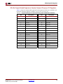
The following table shows the revision history for this document.
Date
Version
Revision
11/22/04
1.0
Initial Xilinx release.
03/04/05
2.0
Renamed title from ML401 Evaluation Platform user guide to ML40x Evaluation Platform
user guide.
Expanded document from ML401-specific to include ML401, ML402, and ML403
platforms.
Added “Building the Linux BSP (PPC405 Systems Only)” section.
07/05/05
3.0
Renamed title from ML40x Evaluation Platform user guide to ML40x EDK Processor
Evaluation Platform user guide.
Updated the user guide for EDK 7.1 release.
Revised the “Building the Linux BSP (PPC405 Systems Only)” section.
02/14/06
4.0
Updated the user guide for EDK 8.1 release.
05/04/06
4.1
Updated “Instructions for Downloading the Design.”
06/30/06
5.0
Expanded to include ML405 evaluation platform.
ML40x EDK Processor Reference Design
www.xilinx.com
UG082 (v5.0) June 30, 2006
Table of Contents
Schedule of Figures . . . . . . . . . . . . . . . . . . . . . . . . . . . . . . . . . . . . . . . . . . . . . . . . . . . . . . . . . .
7
Schedule of Tables . . . . . . . . . . . . . . . . . . . . . . . . . . . . . . . . . . . . . . . . . . . . . . . . . . . . . . . . . . .
9
Preface: About This Guide
Guide Contents . . . . . . . . . . . . . . . . . . . . . . . . . . . . . . . . . . . . . . . . . . . . . . . . . . . . . . . . . . . . . 11
Additional Resources . . . . . . . . . . . . . . . . . . . . . . . . . . . . . . . . . . . . . . . . . . . . . . . . . . . . . . . 11
Conventions . . . . . . . . . . . . . . . . . . . . . . . . . . . . . . . . . . . . . . . . . . . . . . . . . . . . . . . . . . . . . . . . 12
Typographical . . . . . . . . . . . . . . . . . . . . . . . . . . . . . . . . . . . . . . . . . . . . . . . . . . . . . . . . . . . . 12
Online Document . . . . . . . . . . . . . . . . . . . . . . . . . . . . . . . . . . . . . . . . . . . . . . . . . . . . . . . . . 13
Chapter 1: Introduction to the ML40x Embedded Processor Reference
System
Introduction . . . . . . . . . . . . . . . . . . . . . . . . . . . . . . . . . . . . . . . . . . . . . . . . . . . . . . . . . . . . . . . .
Requirements . . . . . . . . . . . . . . . . . . . . . . . . . . . . . . . . . . . . . . . . . . . . . . . . . . . . . . . . . . . . . . .
CoreConnect . . . . . . . . . . . . . . . . . . . . . . . . . . . . . . . . . . . . . . . . . . . . . . . . . . . . . . . . . . . . . . . .
Reference System Information . . . . . . . . . . . . . . . . . . . . . . . . . . . . . . . . . . . . . . . . . . . . . .
Further Reading . . . . . . . . . . . . . . . . . . . . . . . . . . . . . . . . . . . . . . . . . . . . . . . . . . . . . . . . . . . . .
15
15
16
16
17
Resources for EDK Users (Including New Users) . . . . . . . . . . . . . . . . . . . . . . . . . . . . . . 17
Documentation Provided by Xilinx . . . . . . . . . . . . . . . . . . . . . . . . . . . . . . . . . . . . . . . . . . 17
IBM CoreConnect Documentation . . . . . . . . . . . . . . . . . . . . . . . . . . . . . . . . . . . . . . . . . . 17
Chapter 2: ML40x Embedded Processor Reference System
Introduction . . . . . . . . . . . . . . . . . . . . . . . . . . . . . . . . . . . . . . . . . . . . . . . . . . . . . . . . . . . . . . . . 19
Hardware . . . . . . . . . . . . . . . . . . . . . . . . . . . . . . . . . . . . . . . . . . . . . . . . . . . . . . . . . . . . . . . . . . . 19
Overview . . . . . . . . . . . . . . . . . . . . . . . . . . . . . . . . . . . . . . . . . . . . . . . . . . . . . . . . . . . . . . . .
Processor Local Bus (PLB) . . . . . . . . . . . . . . . . . . . . . . . . . . . . . . . . . . . . . . . . . . . . . . . . .
On-Chip Peripheral Bus (OPB) . . . . . . . . . . . . . . . . . . . . . . . . . . . . . . . . . . . . . . . . . . . . .
Device Control Register (DCR) . . . . . . . . . . . . . . . . . . . . . . . . . . . . . . . . . . . . . . . . . . . . .
Interrupts . . . . . . . . . . . . . . . . . . . . . . . . . . . . . . . . . . . . . . . . . . . . . . . . . . . . . . . . . . . . . . . .
Clock/Reset Distribution . . . . . . . . . . . . . . . . . . . . . . . . . . . . . . . . . . . . . . . . . . . . . . . . . .
CPU Debug via JTAG . . . . . . . . . . . . . . . . . . . . . . . . . . . . . . . . . . . . . . . . . . . . . . . . . . . . .
Error LEDs . . . . . . . . . . . . . . . . . . . . . . . . . . . . . . . . . . . . . . . . . . . . . . . . . . . . . . . . . . . . . .
IP Version and Source . . . . . . . . . . . . . . . . . . . . . . . . . . . . . . . . . . . . . . . . . . . . . . . . . . . . .
19
22
23
24
24
25
26
26
26
Synthesis and Implementation . . . . . . . . . . . . . . . . . . . . . . . . . . . . . . . . . . . . . . . . . . . . . .
Design Flow Environment . . . . . . . . . . . . . . . . . . . . . . . . . . . . . . . . . . . . . . . . . . . . . . . . . . .
Memory Map . . . . . . . . . . . . . . . . . . . . . . . . . . . . . . . . . . . . . . . . . . . . . . . . . . . . . . . . . . . . . . .
ML40x Specific Registers . . . . . . . . . . . . . . . . . . . . . . . . . . . . . . . . . . . . . . . . . . . . . . . . . . . .
27
ML40x Board General Purpose I/O Registers . . . . . . . . . . . . . . . . . . . . . . . . . . . . . . . . .
ML40x Control Register 1 . . . . . . . . . . . . . . . . . . . . . . . . . . . . . . . . . . . . . . . . . . . . . . . . . .
ML40x Control Register 2 . . . . . . . . . . . . . . . . . . . . . . . . . . . . . . . . . . . . . . . . . . . . . . . . . .
ML40x Character LCD General Purpose I/O Registers . . . . . . . . . . . . . . . . . . . . . . . . .
ML40x EDK Processor Reference Design
UG082 (v5.0) June 30, 2006
www.xilinx.com
27
28
29
29
30
31
32
3
R
ML40x Differential Expansion Header General Purpose I/O Registers . . . . . . . . . . . 32
ML40x Single-Ended Expansion Header General Purpose I/O Registers . . . . . . . . . 33
Extending or Modifying the Design . . . . . . . . . . . . . . . . . . . . . . . . . . . . . . . . . . . . . . . . . 34
Adding or Removing IP Cores . . . . . . . . . . . . . . . . . . . . . . . . . . . . . . . . . . . . . . . . . . . . . . 34
Chapter 3: EDK Tutorial and Demonstration
Introduction . . . . . . . . . . . . . . . . . . . . . . . . . . . . . . . . . . . . . . . . . . . . . . . . . . . . . . . . . . . . . . . . 35
Instructions for Invoking the EDK tools . . . . . . . . . . . . . . . . . . . . . . . . . . . . . . . . . . . . . 35
Launching Xilinx Platform Studio (XPS) . . . . . . . . . . . . . . . . . . . . . . . . . . . . . . . . . . . . . 36
Instructions for Selecting Software Application. . . . . . . . . . . . . . . . . . . . . . . . . . . . . . 36
Instructions for Building and Implementing the Design . . . . . . . . . . . . . . . . . . . . . 36
Instructions for Downloading the Design. . . . . . . . . . . . . . . . . . . . . . . . . . . . . . . . . . . . 37
Download Using Parallel Cable IV or Platform Cable USB (iMPACT Program). . . . 37
Download Using the System ACE Interface . . . . . . . . . . . . . . . . . . . . . . . . . . . . . . . . . . 38
Software . . . . . . . . . . . . . . . . . . . . . . . . . . . . . . . . . . . . . . . . . . . . . . . . . . . . . . . . . . . . . . . . . . . . 39
Building the Linux BSP (PPC405 Systems Only) . . . . . . . . . . . . . . . . . . . . . . . . . . . . . 41
Chapter 4: Introduction to Hardware Reference IP
Introduction . . . . . . . . . . . . . . . . . . . . . . . . . . . . . . . . . . . . . . . . . . . . . . . . . . . . . . . . . . . . . . . . 43
Hardware Reference IP Source Format and Size. . . . . . . . . . . . . . . . . . . . . . . . . . . . . . 44
Chapter 5: Using IPIF to Build IP
Introduction . . . . . . . . . . . . . . . . . . . . . . . . . . . . . . . . . . . . . . . . . . . . . . . . . . . . . . . . . . . . . . . . 45
SRAM Protocol Overview of IPIF . . . . . . . . . . . . . . . . . . . . . . . . . . . . . . . . . . . . . . . . . . . 46
Basic Write Transactions . . . . . . . . . . . . . . . . . . . . . . . . . . . . . . . . . . . . . . . . . . . . . . . . . . . 47
Basic Read Transactions . . . . . . . . . . . . . . . . . . . . . . . . . . . . . . . . . . . . . . . . . . . . . . . . . . . 48
IPIF Status and Control Signals . . . . . . . . . . . . . . . . . . . . . . . . . . . . . . . . . . . . . . . . . . . . . 48
Using IPIF to Create a GPIO Peripheral from Scratch . . . . . . . . . . . . . . . . . . . . . . . . 48
Using IPIF to Connect a Pre-Existent Peripheral to the Bus . . . . . . . . . . . . . . . . . . . 50
Conclusion . . . . . . . . . . . . . . . . . . . . . . . . . . . . . . . . . . . . . . . . . . . . . . . . . . . . . . . . . . . . . . . . . . 51
Chapter 6: OPB AC97 Sound Controller
Overview . . . . . . . . . . . . . . . . . . . . . . . . . . . . . . . . . . . . . . . . . . . . . . . . . . . . . . . . . . . . . . . . . . .
Related Documents . . . . . . . . . . . . . . . . . . . . . . . . . . . . . . . . . . . . . . . . . . . . . . . . . . . . . . . . .
Features . . . . . . . . . . . . . . . . . . . . . . . . . . . . . . . . . . . . . . . . . . . . . . . . . . . . . . . . . . . . . . . . . . . . .
Module Port Interface . . . . . . . . . . . . . . . . . . . . . . . . . . . . . . . . . . . . . . . . . . . . . . . . . . . . . . .
Implementation . . . . . . . . . . . . . . . . . . . . . . . . . . . . . . . . . . . . . . . . . . . . . . . . . . . . . . . . . . . . .
Memory Map . . . . . . . . . . . . . . . . . . . . . . . . . . . . . . . . . . . . . . . . . . . . . . . . . . . . . . . . . . . . . . .
53
53
53
54
56
57
Chapter 7: OPB PS/2 Controller (Dual)
Overview . . . . . . . . . . . . . . . . . . . . . . . . . . . . . . . . . . . . . . . . . . . . . . . . . . . . . . . . . . . . . . . . . . .
Related Documents . . . . . . . . . . . . . . . . . . . . . . . . . . . . . . . . . . . . . . . . . . . . . . . . . . . . . . . . .
Features . . . . . . . . . . . . . . . . . . . . . . . . . . . . . . . . . . . . . . . . . . . . . . . . . . . . . . . . . . . . . . . . . . . . .
Module Port Interface . . . . . . . . . . . . . . . . . . . . . . . . . . . . . . . . . . . . . . . . . . . . . . . . . . . . . . .
4
www.xilinx.com
61
61
61
62
ML40x EDK Processor Reference Design
UG082 (v5.0) June 30, 2006
R
Implementation . . . . . . . . . . . . . . . . . . . . . . . . . . . . . . . . . . . . . . . . . . . . . . . . . . . . . . . . . . . . . 64
Memory Map . . . . . . . . . . . . . . . . . . . . . . . . . . . . . . . . . . . . . . . . . . . . . . . . . . . . . . . . . . . . . . . 65
Chapter 8: PLB TFT LCD Controller
Overview . . . . . . . . . . . . . . . . . . . . . . . . . . . . . . . . . . . . . . . . . . . . . . . . . . . . . . . . . . . . . . . . . . .
Related Documents . . . . . . . . . . . . . . . . . . . . . . . . . . . . . . . . . . . . . . . . . . . . . . . . . . . . . . . . .
Features . . . . . . . . . . . . . . . . . . . . . . . . . . . . . . . . . . . . . . . . . . . . . . . . . . . . . . . . . . . . . . . . . . . . .
Module Port Interface . . . . . . . . . . . . . . . . . . . . . . . . . . . . . . . . . . . . . . . . . . . . . . . . . . . . . . .
Hardware . . . . . . . . . . . . . . . . . . . . . . . . . . . . . . . . . . . . . . . . . . . . . . . . . . . . . . . . . . . . . . . . . . .
71
71
71
71
75
Implementation . . . . . . . . . . . . . . . . . . . . . . . . . . . . . . . . . . . . . . . . . . . . . . . . . . . . . . . . . . 75
Video Timing . . . . . . . . . . . . . . . . . . . . . . . . . . . . . . . . . . . . . . . . . . . . . . . . . . . . . . . . . . . . 76
Memory Map . . . . . . . . . . . . . . . . . . . . . . . . . . . . . . . . . . . . . . . . . . . . . . . . . . . . . . . . . . . . . . . 78
Video Memory . . . . . . . . . . . . . . . . . . . . . . . . . . . . . . . . . . . . . . . . . . . . . . . . . . . . . . . . . . . 78
Control Registers (DCR Interface) . . . . . . . . . . . . . . . . . . . . . . . . . . . . . . . . . . . . . . . . . . . 79
ML40x EDK Processor Reference Design
UG082 (v5.0) June 30, 2006
www.xilinx.com
5
R
6
www.xilinx.com
ML40x EDK Processor Reference Design
UG082 (v5.0) June 30, 2006
Schedule of Figures
Chapter 1: Introduction to the ML40x Embedded Processor Reference
System
Chapter 2: ML40x Embedded Processor Reference System
Figure 2-1: Hardware View of ML40x Embedded MicroBlaze Reference System . . . . . 20
Figure 2-2: Hardware View of ML40x Embedded PPC405 Reference System . . . . . . . . . 21
Figure 2-3: Clock Generation . . . . . . . . . . . . . . . . . . . . . . . . . . . . . . . . . . . . . . . . . . . . . . . . . . . 25
Chapter 3: EDK Tutorial and Demonstration
Chapter 4: Introduction to Hardware Reference IP
Chapter 5: Using IPIF to Build IP
Figure 5-1: IPIF SRAM Module Interface . . . . . . . . . . . . . . . . . . . . . . . . . . . . . . . . . . . . . . . . 46
Figure 5-2: IPIF Simple SRAM Write Cycle . . . . . . . . . . . . . . . . . . . . . . . . . . . . . . . . . . . . . . 47
Figure 5-3: IPIF Simple SRAM Read Cycle. . . . . . . . . . . . . . . . . . . . . . . . . . . . . . . . . . . . . . . 48
Figure 5-4: IPIF SRAM Module to GPIO Logic Interface. . . . . . . . . . . . . . . . . . . . . . . . . . . 49
Chapter 6: OPB AC97 Sound Controller
Figure 6-1: OPB AC97 Sound Controller Block Diagram. . . . . . . . . . . . . . . . . . . . . . . . . . . 56
Chapter 7: OPB PS/2 Controller (Dual)
Figure 7-1: OPB PS/2 Controller Block Diagram . . . . . . . . . . . . . . . . . . . . . . . . . . . . . . . . . . 64
Chapter 8: PLB TFT LCD Controller
Figure 8-1: High-Level Block Diagram. . . . . . . . . . . . . . . . . . . . . . . . . . . . . . . . . . . . . . . . . . . 75
Figure 8-2: Hsync and TFT Clock . . . . . . . . . . . . . . . . . . . . . . . . . . . . . . . . . . . . . . . . . . . . . . . 76
Figure 8-3: Horizontal Data . . . . . . . . . . . . . . . . . . . . . . . . . . . . . . . . . . . . . . . . . . . . . . . . . . . . 76
Figure 8-4: Vsync and h_syncs . . . . . . . . . . . . . . . . . . . . . . . . . . . . . . . . . . . . . . . . . . . . . . . . . . 77
Figure 8-5: Vertical Data . . . . . . . . . . . . . . . . . . . . . . . . . . . . . . . . . . . . . . . . . . . . . . . . . . . . . . . 77
ML40x EDK Processor Reference Design
UG082 (v5.0) June 30, 2006
www.xilinx.com
7
R
8
www.xilinx.com
ML40x EDK Processor Reference Design
UG082 (v5.0) June 30, 2006
Schedule of Tables
Chapter 1: Introduction to the ML40x Embedded Processor Reference
System
Chapter 2: ML40x Embedded Processor Reference System
Table 2-1: IP Cores in the ML40x Embedded Processor Reference System. . . . . . . . . . . . 26
Table 2-2: Memory Maps. . . . . . . . . . . . . . . . . . . . . . . . . . . . . . . . . . . . . . . . . . . . . . . . . . . . . . . 28
Table 2-3: GPIO Registers (Address 0x90000000-0x90000004) . . . . . . . . . . . . . . . . . . . . . . . 29
Table 2-4: Control Register 1 (Address 0x90000008). . . . . . . . . . . . . . . . . . . . . . . . . . . . . . . . 30
Table 2-5: Control Register 2 (Address 0x9000000C) . . . . . . . . . . . . . . . . . . . . . . . . . . . . . . . 31
Table 2-6: Character LCD GPIO Registers (Address 0x90002000-0x90002004) . . . . . . . . . 32
Table 2-7: Differential Expansion Header GPIO Regs (Addr 0x90001000-0x90001004) . 32
Table 2-8: Single-Ended Expansion Header GPIO Regs (Addr 0x90001008-0x9000100C) 33
Chapter 3: EDK Tutorial and Demonstration
Table 3-1: Demonstration Software Applications . . . . . . . . . . . . . . . . . . . . . . . . . . . . . . . . . 39
Chapter 4: Introduction to Hardware Reference IP
Table 4-1: Hardware Reference IP and Logic Utilization . . . . . . . . . . . . . . . . . . . . . . . . . . . 44
Chapter 5: Using IPIF to Build IP
Chapter 6: OPB AC97 Sound Controller
Table 6-1: Global Signals . . . . . . . . . . . . . . . . . . . . . . . . . . . . . . . . . . . . . . . . . . . . . . . . . . . . . . 54
Table 6-2: OPB Slave Signals . . . . . . . . . . . . . . . . . . . . . . . . . . . . . . . . . . . . . . . . . . . . . . . . . . . 54
Table 6-3: External I/O Pins . . . . . . . . . . . . . . . . . . . . . . . . . . . . . . . . . . . . . . . . . . . . . . . . . . . . 54
Table 6-4: Generics (Parameters) . . . . . . . . . . . . . . . . . . . . . . . . . . . . . . . . . . . . . . . . . . . . . . . . 55
Table 6-5: Memory Map. . . . . . . . . . . . . . . . . . . . . . . . . . . . . . . . . . . . . . . . . . . . . . . . . . . . . . . . 57
Chapter 7: OPB PS/2 Controller (Dual)
Table 7-1: OPB Slave Signals . . . . . . . . . . . . . . . . . . . . . . . . . . . . . . . . . . . . . . . . . . . . . . . . . . . 62
Table 7-2: External I/O Pins . . . . . . . . . . . . . . . . . . . . . . . . . . . . . . . . . . . . . . . . . . . . . . . . . . . . 62
Table 7-3: Parameters . . . . . . . . . . . . . . . . . . . . . . . . . . . . . . . . . . . . . . . . . . . . . . . . . . . . . . . . . . 63
Table 7-4: Memory Map Table . . . . . . . . . . . . . . . . . . . . . . . . . . . . . . . . . . . . . . . . . . . . . . . . . . 65
Table 7-5: OPB PS/2 Slave Device Pin Description . . . . . . . . . . . . . . . . . . . . . . . . . . . . . . . . 66
Chapter 8: PLB TFT LCD Controller
Table 8-1: Global Signals . . . . . . . . . . . . . . . . . . . . . . . . . . . . . . . . . . . . . . . . . . . . . . . . . . . . . . 71
ML40x EDK Processor Reference Design
UG082 (v5.0) June 30, 2006
www.xilinx.com
9
R
Table 8-2: PLB Master Signals . . . . . . . . . . . . . . . . . . . . . . . . . . . . . . . . . . . . . . . . . . . . . . . . . . 72
Table 8-3: DCR Slave Signals . . . . . . . . . . . . . . . . . . . . . . . . . . . . . . . . . . . . . . . . . . . . . . . . . . . 73
Table 8-4: External Output Pins . . . . . . . . . . . . . . . . . . . . . . . . . . . . . . . . . . . . . . . . . . . . . . . . . 73
Table 8-5: Parameters . . . . . . . . . . . . . . . . . . . . . . . . . . . . . . . . . . . . . . . . . . . . . . . . . . . . . . . . . . 74
Table 8-6: Pixel Color Encoding . . . . . . . . . . . . . . . . . . . . . . . . . . . . . . . . . . . . . . . . . . . . . . . . . 78
Table 8-7: Control Registers (DCR Interface) . . . . . . . . . . . . . . . . . . . . . . . . . . . . . . . . . . . . . 79
10
www.xilinx.com
ML40x EDK Processor Reference Design
UG082 (v5.0) June 30, 2006
R
Preface
About This Guide
This user guide documents the ML40x reference design.
Guide Contents
This user guide contains the following chapters:
•
Chapter 1, “Introduction to the ML40x Embedded Processor Reference System”
•
Chapter 2, “ML40x Embedded Processor Reference System”
•
Chapter 3, “EDK Tutorial and Demonstration”
•
Chapter 4, “Introduction to Hardware Reference IP”
•
Chapter 5, “Using IPIF to Build IP”
•
Chapter 6, “OPB AC97 Sound Controller”
•
Chapter 7, “OPB PS/2 Controller (Dual)”
•
Chapter 8, “PLB TFT LCD Controller”
Additional Resources
To find additional documentation, see the Xilinx website at:
http://www.xilinx.com/literature.
To search the Answer Database of silicon, software, and IP questions and answers, or to
create a technical support WebCase, see the Xilinx website at:
http://www.xilinx.com/support.
ML40x EDK Processor Reference Design
UG082 (v5.0) June 30, 2006
www.xilinx.com
11
R
Preface: About This Guide
Conventions
This document uses the following conventions. An example illustrates each convention.
Typographical
The following typographical conventions are used in this document:
Convention
Meaning or Use
Courier font
Messages, prompts, and
program files that the system
displays
speed grade: - 100
Courier bold
Literal commands that you enter
in a syntactical statement
ngdbuild design_name
Commands that you select from
a menu
File → Open
Keyboard shortcuts
Ctrl+C
Variables in a syntax statement
for which you must supply
values
ngdbuild design_name
References to other manuals
See the Development System
Reference Guide for more
information.
Emphasis in text
If a wire is drawn so that it
overlaps the pin of a symbol, the
two nets are not connected.
An optional entry or parameter.
However, in bus specifications,
such as bus[7:0], they are
required.
ngdbuild [option_name]
design_name
A list of items from which you
must choose one or more
lowpwr ={on|off}
Separates items in a list of
choices
lowpwr ={on|off}
Vertical ellipsis
.
.
.
Repetitive material that has
been omitted
IOB #1: Name = QOUT’
IOB #2: Name = CLKIN’
.
.
.
Horizontal ellipsis . . .
Repetitive material that has
been omitted
allow block block_name loc1
loc2 ... locn;
Helvetica bold
Italic font
Square brackets
Braces
[ ]
{ }
Vertical bar
12
Example
|
www.xilinx.com
ML40x EDK Processor Reference Design
UG082 (v5.0) June 30, 2006
R
Conventions
Online Document
The following conventions are used in this document:
Convention
Meaning or Use
Example
See the section “Additional
Resources” for details.
Blue text
Cross-reference link to a location
in the current document
Red text
Cross-reference link to a location
in another document
See Figure 2-5 in the Virtex-II
Platform FPGA User Guide.
Blue, underlined text
Hyperlink to a website (URL)
Go to http://www.xilinx.com
for the latest speed files.
ML40x EDK Processor Reference Design
UG082 (v5.0) June 30, 2006
www.xilinx.com
Refer to “Title Formats” in
Chapter 1 for details.
13
R
Preface: About This Guide
14
www.xilinx.com
ML40x EDK Processor Reference Design
UG082 (v5.0) June 30, 2006
R
Chapter 1
Introduction to the ML40x Embedded
Processor Reference System
Introduction
This chapter briefly describes the reference system provided for ML40x evaluation
platforms. The ML40x Embedded Processor Reference System contains a combination of
known working hardware and software elements that, together, create an entire system. It
demonstrates a system using the Processor Local Bus (PLB), On-Chip Peripheral Bus
(OPB), Device Control Register (DCR) Bus, and the PowerPC™ 405 or MicroBlaze™
processor core. The design operates under the Embedded Development Kit (EDK) suite of
tools that provides a graphical tool framework for designing embedded hardware and
software. The reference system is intended to familiarize users with the Virtex™-4
product, its design tool flows, and its features. It provides a foundation for those who are
learning how to use embedded processors in Virtex-4 FPGAs.
This document covers MicroBlaze based systems for ML401, ML402, ML403 boards in
addition to PowerPC 405 based systems for the ML403 and ML405 boards.
Requirements
The following hardware and software are required in order to use the ML40x Embedded
Processor Reference System.
•
Operating System Requirements:
♦
Windows XP Professional or Linux
Note: A PC is required for FPGA download and debug via Xilinx download cables.
•
Hardware Requirements:
♦
•
Xilinx ML401, ML402, ML403, or ML405 evaluation platform
Software Requirements:
♦
♦
Embedded Development Kit (EDK) 8.1
-
Service Pack 1 for ML401, ML402, ML403
-
Service Pack 2 for ML405
ISE 8.1i
-
Service Pack 2 for ML01, ML402, ML403
-
Service Pack 3 for ML405
ML40x EDK Processor Reference Design
UG082 (v5.0) June 30, 2006
www.xilinx.com
15
Chapter 1: Introduction to the ML40x Embedded Processor Reference System
R
For new EDK users, the ML40x Embedded Processor Reference System provides an
excellent example of how the EDK tools can be used to design a full featured embedded
system consisting of hardware and software. The reference system also illustrates how to
debug designs under EDK.
References to additional information about learning to use EDK is available in “Further
Reading,” page 17.
CoreConnect
Download and installation of the IBM CoreConnect Toolkit can be useful for hardware and
systems. The CoreConnect Toolkit is only available to CoreConnect licensees. Xilinx has
simplified the process of becoming a CoreConnect licensee through Web-based
registration available at http://www.xilinx.com/coreconnect. CoreConnect licensees are
entitled to full access to the CoreConnect Toolkit including powerful bus functional
modeling, bus monitoring tools, and periodic updates. To get the most out of the
Embedded Development Kit, Xilinx recommends the use of the IBM CoreConnect Toolkit.
Reference System Information
This section is an overview of the features of the ML40x Embedded Processor Reference
System. Although the information contained in the reference system chapter is not
exhaustive, it covers the basic requirements to effectively use the MicroBlaze or PowerPC
processor. Chapter 2, “ML40x Embedded Processor Reference System” and Chapter 3,
“EDK Tutorial and Demonstration” have instructions on how to synthesize and run the
designs through the Xilinx Implementation Tools (ISE) for the Virtex-4 family.
The reference system chapters contain sections about:
•
Hardware used in the system
•
HDL file organization
•
Synthesis and implementation
•
Software applications that interoperate with the system
•
Instructions to run the software applications
The ML40x Embedded Processor Reference System is an example of a completely
embedded computer. It provides a wide variety of memory interfaces on three differing
buses, as well as various peripherals such as memory controllers, general purpose I/O
(GPIO), and UARTs. The example software provided with this reference system is
designed to demonstrate the system running a stand-alone application.
The Embedded Processor Reference System provides additional study of the PLB, OPB,
and DCR buses. In addition, it affords the opportunity to see how OPB-based devices are
used in a system. Step-by-step instructions are provided to help the user through the
design flow and to target a Virtex-4 device. Users can modify the ML40x Embedded
Processor Reference System to add and subtract peripherals, as well as to change the
software for their own custom-designed systems. These designs can be synthesized and
run through place-and-route to produce a bitstream for Virtex-4 devices.
Note: The README file in the EDK project directory of the reference design contains important
release notes and information about the design.
16
www.xilinx.com
ML40x EDK Processor Reference Design
UG082 (v5.0) June 30, 2006
R
Further Reading
Further Reading
Xilinx provides a wealth of valuable information to assist you in your design efforts. Some
of the relevant documentation is listed below with more information available through the
Xilinx Support website at http://www.xilinx.com/support. To obtain the most recent
revision of documentation related to the ML40x board, see the corresponding Web page:
•
ML401: http://www.xilinx.com/ml401
•
ML402: http://www.xilinx.com/ml402
•
ML403: http://www.xilinx.com/ml403
•
ML405: http://www.xilinx.com/ml405
Resources for EDK Users (Including New Users)
EDK Main Web Page
http://www.xilinx.com/ise/embedded/edk.htm
Getting Started with the EDK
http://www.xilinx.com/ise/embedded/edk_getstarted.pdf
Embedded System Tools Guide
http://www.xilinx.com/ise/embedded/est_guide.pdf
EDK Tutorials and Design Examples
http://www.xilinx.com/ise/embedded/edk_examples.htm
Embedded Processor Discussion Forum
http://toolbox.xilinx.com/cgi-bin/forum?14@@/Embedded%20Processors
Documentation Provided by Xilinx
Virtex-4 Data Sheet: DC and Switching Characteristics
http://www.xilinx.com/bvdocs/publications/ds302.pdf
Virtex-4 User Guide
http://www.xilinx.com/bvdocs/userguides/ug070.pdf
IBM CoreConnect Documentation
The Embedded Development Kit integrates with the IBM CoreConnect Toolkit. The toolkit
provides a number of features, enhancing design productivity and allowing you to get the
most from the EDK. To obtain the toolkit, you must be a licensee of the IBM CoreConnect
Bus Architecture. Licensing CoreConnect provides access to a wealth of documentation,
Bus Functional Models, Hardware IP, and the toolkit.
Xilinx provides a Web-based licensing mechanism that allows you to obtain the
CoreConnect toolkit from our website. To license CoreConnect, use an Internet browser to
access http://www.xilinx.com/ipcenter/processor_central/register_coreconnect.htm.
After your request has been approved (typically within 24 hours), you will receive an
e-mail granting access to a protected website. You can then download the toolkit. If you
prefer, you can also license CoreConnect directly from IBM.
If you would like further information on CoreConnect Bus Architecture, see IBM's
CoreConnect website at http://www.ibm.com/chips/products/coreconnect.
ML40x EDK Processor Reference Design
UG082 (v5.0) June 30, 2006
www.xilinx.com
17
Chapter 1: Introduction to the ML40x Embedded Processor Reference System
18
www.xilinx.com
R
ML40x EDK Processor Reference Design
UG082 (v5.0) June 30, 2006
R
Chapter 2
ML40x Embedded Processor Reference
System
Introduction
The ML40x Embedded Processor Reference System is an example of a large Virtex-4 based
system. An IBM Core Connect infrastructure connects the CPU to numerous peripherals
using Processor Local Bus (PLB), On-Chip Peripheral Bus (OPB), and Device Control
Register (DCR) buses to build a complete system. This document describes the contents of
the reference system and provides information about how the system is organized and
implemented. A complete design cycle incorporating synthesis, FPGA implementation,
and download is described. The information introduces many aspects of the ML40x
Embedded Processor Reference System, but the user should refer to additional specific
documentation for more detailed information about the software, tools, peripherals,
interface protocols, and capabilities of the FPGA.
Hardware
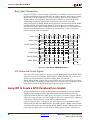
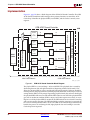
Overview
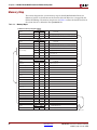
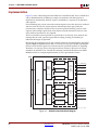
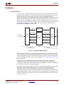
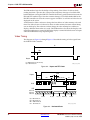
Figure 2-1, page 20 provides a high-level view of the hardware contents of the Embedded
MicroBlaze Processor System. Figure 2-2, page 21 provides an overview of the
PPC405-based system for ML403. These designs demonstrate a system that uses PLB, OPB,
and DCR devices. The PLB protocol generally supports higher bandwidths, so the highbandwidth devices are placed there. The OPB connects the lower-performance peripheral
devices to the CPU. The OPB offers a less complex protocol relative to the PLB, making it
easier to design peripherals that do not require the highest performance. The OPB also has
the advantage that it can support a greater number of devices. DCR is used with control
and status registers for simplicity when performance is not important. Refer to the PLB,
OPB, and DCR CoreConnect Architecture Specifications for more information. The
hardware devices used in this design are described in more detail in the Processor IP
Reference Guide (see <EDK Install Directory>/doc/proc_ip_ref_guide.pdf)
and in Chapter 4, “Introduction to Hardware Reference IP.”
ML40x EDK Processor Reference Design
UG082 (v5.0) June 30, 2006
www.xilinx.com
19
R
IPIF
GPIO
Char
LCD
IPIF
Chapter 2: ML40x Embedded Processor Reference System
GPIO
Expansion
Header
LMBBRAM CTLR
BRAM
DLMB
MicroBlaze
INT
ILMB
IPIF
IPIF
IPIF
IPIF
MDM
PS/2
PS/2
IPIF
DDR
Memory
Ethernet
GPIO
GPIO
IPIF
DDR
MEMC
System ACE
MPU
UART
IPIF
TFT
LCD
Controller
INTC
IPIF
LMBBRAM CTLR
EMC
ZBT
SRAM
Flash
IPIF
EMC
IPIF
AC97
Sound
Ctlr
IPIF
OPB2PLB
Bridge
PLB
ARB
Buttons, LEDs, IIC,
and misc. I/Os
DCR
Bridge
USB
Memory Mapped
DCR Bus
OPB
ARB
UG082_02_01_050406
Figure 2-1: Hardware View of ML40x Embedded MicroBlaze Reference System
20
www.xilinx.com
ML40x EDK Processor Reference Design
UG082 (v5.0) June 30, 2006
R
IPIF
Char
LCD
GPIO
Expansion
Header
ISPLB
IPIF
DSPLB
INTC
IPIF
BRAM
System ACE
MPU
IPIF
BRAM
MEMC
PPC405
Processor Block
GPIO
IPIF
Hardware
Ethernet
IPIF
PLB2OPB
Bridge
IPIF
DDR
Memory
IPIF
DDR
MEMC
IIC
GPIO
GPIO
IPIF
TFT
LCD
Controller
PS/2
PS/2
UART
IPIF
INT
EMC
Buttons, LEDs, IIC,
and misc. I/Os
ZBT
SRAM
PLB
ARB
IPIF
EMC
IPIF
AC97
Sound
Controller
IPIF
Flash
DCR
Bridge
USB
Memory Mapped
DCR Bus
OPB
ARB
UG082_02_02_050406
Figure 2-2:
ML40x EDK Processor Reference Design
UG082 (v5.0) June 30, 2006
Hardware View of ML40x Embedded PPC405 Reference System
www.xilinx.com
21
R
Chapter 2: ML40x Embedded Processor Reference System
Processor Local Bus (PLB)
The PLB connects the CPU to high-performance devices, such as memory controllers. The
PLB protocol supports higher bandwidth transactions and has a feature set better than
OPB/DCR. PLB supports memory operations OPB/DCR. Highlights of the PLB protocol
include synchronous architecture, independent read/write data paths, and split
transaction address/data buses. The reference design includes a 64-bit PLB infrastructure
with 64-bit master and slave devices attached.
The PLB devices in the reference system include:
•
•
•
PLB Masters
♦
640x480 VGA Controller
♦
OPB-to-PLB Bridge (MicroBlaze system)
♦
PPC405 Instruction-Side PLB Interface (PPC405 system)
♦
PPC405 Data-Side PLB Interface (PPC405 system)
PLB Slaves
♦
Double Data Rate (DDR) SDRAM Controller
♦
BRAM Controller (PPC405 systems)
♦
PLB-to-OPB Bridge (PPC405 system)
PLB Arbiter
♦
64-bit Xilinx PLB Arbiter
In general, all PLB devices are optimized around the FPGA architecture and use pipelining
to improve maximum clock frequencies and reduce logic utilization. Refer to the
documentation accompanying each device for more information about its design.
22
www.xilinx.com
ML40x EDK Processor Reference Design
UG082 (v5.0) June 30, 2006
R
Hardware
On-Chip Peripheral Bus (OPB)
The OPB connects lower-performance peripheral devices to the system. The OPB has a less
complex architecture, simplifying peripheral development. OPB and PLB devices can
communicate by way of an OPB-to-PLB Bridge or an PLB-to-OPB Bridge.
The OPB devices in the reference system include:
•
•
•
OPB Masters
♦
Ethernet Controller (DMA Engine, if enabled)
♦
MicroBlaze Processor Instruction-Side Interface (MicroBlaze system)
♦
MicroBlaze Processor Data-Side Interface (MicroBlaze system)
♦
PLB-to-OPB Bridge (PPC405 system)
OPB Slaves
♦
IIC Controller (PPC405 system)
♦
General-Purpose Input/Output (GPIO) x3
♦
16450 UART
♦
Interrupt Controller
♦
External Memory Controller x2
♦
Microprocessor Debug Module (MicroBlaze system)
♦
AC97 Sound Controller
♦
OPB-to-DCR Bridge
♦
Ethernet Controller
♦
Dual PS/2 Controller
♦
System ACE™ MPU Interface
♦
OPB-to-PLB Bridge-In (MicroBlaze system)
OPB Arbiter
In general, all OPB devices are optimized around the FPGA architecture and make use of
pipelining to improve maximum clock frequencies and reduce logic utilization. Refer to
the accompanying documentation for each device for more information about its design.
The OPB devices in the reference design make use of Intellectual Property InterFace (IPIF)
modules to further simplify IP development. The IPIF converts the OPB protocol into
common interfaces, such as an SRAM protocol or a control register interface. IPIF modules
also provide support for DMA and interrupt functionality. IPIF modules simplify software
development because the IPIF framework has many common features. Refer to Chapter 5,
“Using IPIF to Build IP” for more information.
The IPIF is designed mainly to support a wide variety of common interfaces, but might not
be the optimal solution in all cases. Where additional performance or functionality is
required, the user can develop a custom OPB interface. The IPIF protocols can also be
extended to support other bus standards, such as PLB. This allows the backend interface to
the IP to remain the same while the bus interface logic in the IPIF is changed. This provides
an efficient means for supporting different bus standards with the same IP device.
The OPB specification supports masters and slaves of up to 64 bits with a dynamic bus sizing
capability that allows OPB masters and slaves of different sizes to communicate with each
other. The ML40x Embedded Processor Reference System uses a subset of the OPB
specification that supports only 32-bit byte enable masters and slaves. Legacy devices
utilizing 8- or 16-bit interfaces or those that require dynamic bus sizing functionality are
not directly supported. It is recommended that all new OPB peripherals support
byte-enable operations for better performance and reduced logic utilization.
ML40x EDK Processor Reference Design
UG082 (v5.0) June 30, 2006
www.xilinx.com
23
R
Chapter 2: ML40x Embedded Processor Reference System
Device Control Register (DCR)
The DCR bus offers a very simple interface protocol and is used for accessing control and
status registers in various devices. It allows for register access to various devices without
overloading the OPB and PLB interfaces. Because DCR devices are generally accessed
infrequently and do not have high-performance requirements, they are used throughout
the reference design for functions, such as error status registers, interrupt controllers, and
device initialization logic.
An OPB-to-DCR Bridge is instantiated to locate the 4-KB DCR space within the general
system memory space. The DCR slave devices connected to the OPB-to-DCR Bridge
include:
•
PLB Arbiter (if enabled)
•
VGA TFT LCD Controller
The DCR specification requires that the DCR master and slave clocks be synchronous to
each other and related in frequency by an integer multiple. It is important to be aware of
the clock domains of each of the DCR devices to ensure proper functionality.
Interrupts
An interrupt controller for interrupts is controlled through the OPB. It allows multiple
edge or level sensitive interrupts from peripherals to be OR'ed together back to the CPU.
The ability for bitwise masking of individual interrupts is also provided. The connections
from the IP to the interrupt controller are:
24
•
UART
•
Microprocessor debug module (MicroBlaze system)
•
Ethernet controller
•
PS/2 Port #1
•
PS/2 Port #2
•
External USB chip
•
System ACE MPU
•
AC97 sound controller (play buffer)
•
AC97 sound controller (record buffer)
•
Ethernet PHY
•
IIC controller (PPC405 system)
www.xilinx.com
ML40x EDK Processor Reference Design
UG082 (v5.0) June 30, 2006
R
Hardware
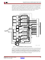
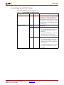
Clock/Reset Distribution
Virtex-4 FPGAs have abundant clock management and global clock buffer resources. To
demonstrate some of these capabilities, the ML40x Embedded Processor Reference System
uses a variety of different clocks. Figure 2-3, page 25 illustrates use of the digital clock
managers (DCMs) for generating the main clocks in the design. A 100-MHz input reference
clock is used to generate the main 100-MHz PLB, OPB, and DCR clocks. The
CLK90/180/270 output of the DCM produces a 100-MHz clock that is phase shifted by
90/180/270 degrees for use by the DDR SDRAM controller. The CLKFX output of the
DCM produces a 300-MHz processor clock for PPC405 designs. The main 100-MHz clock is
divided by four to create a 25-MHz VGA clock. A second DCM is used to recover and
deskew the external clock from the DDR SDRAM. A third DCM (not shown) is used to
deskew the externally driven SRAM clock with the internal 100-MHz clock.
Because each clock is referenced from the same 100-MHz clock, they are all phase aligned
to each other. This synchronous phase alignment is required by the CPU and many other
devices so they can pass signals from one clock domain to another.
Digital Clock
Manager 1
100 MHz
CLK1X
100 MHz +90°
CLK90
External
Reference
Clock
100 MHz
PLB/OPB/OCM
100 MHz +180°
CLK180
IN
DDR
Controller
100 MHz +270°
CLK270
25 MHz
CLKDV
VGA
300 MHz
CLKFX
PPC405
Off-chip connection for board deskew
(not used in
MicroBlaze systems)
Digital Clock
Manager 2
CLK90
IN
CLK270
100 MHz +90°
100 MHz +270°
DDR
Controller
UG082_02_03_050406
Figure 2-3:
Clock Generation
After a system reset or at FPGA startup, a debounce circuit inside the Processor System
Reset IP Module holds the FPGA in reset until the DCM has locked onto its reference clock.
Once the DCM is locked and the clocks remain stable for several cycles, the reset condition
is released to allow the system logic to begin operating. For example, the CPU begins
fetching instructions a few cycles after reset is released. Because the reset net is a highfanout signal, it might not be able to reach all the logic in the design within one clock cycle.
User IP blocks should be designed to take into account the possible skew in the global reset
and still start up properly. Alternatively, the global reset can be registered locally in each IP
block to generate a synchronous reset signal.
ML40x EDK Processor Reference Design
UG082 (v5.0) June 30, 2006
www.xilinx.com
25
R
Chapter 2: ML40x Embedded Processor Reference System
CPU Debug via JTAG
The CPU in the ML40x Embedded Processor Reference System can be debugged via JTAG
using the EDK tools.
The preferred method of communicating with the CPU via JTAG is to combine the CPU
JTAG chain with the FPGA's main JTAG chain, which is also used to download bitstreams.
For MicroBlaze designs, this method requires the user to instantiate an OPB MDM
component and directly connect it to the CPU in the user's design. For PPC405 designs, a
JTAGPPC component must be instantiated and connected to the PPC405 processor. The
primary advantage of sharing the same JTAG chain for CPU debug and FPGA
programming is that this simplifies the number of cables needed; a single JTAG cable (like
the Xilinx Parallel Cable IV cable) can be used for bitstream download as well as CPU
software debugging.
Error LEDs
The design contains two* error LED outputs to signal OPB (Error 1) and PLB (Error 2)
errors. OPB errors (Error 1 LED on the ML40x board) signal an OPB timeout or OPB error
acknowledge condition. PLB errors (Error 2 LED on the ML40x board) signal a PLB
timeout or data error acknowledge condition as reported by the PLB arbiter. Control
registers in the design allow the error conditions to be cleared. See “ML40x Control
Register 2,” page 31 for more information.
Note: *On the ML403 and ML405 boards, only the Error 1 LED is present. It signals both PLB and
OPB error conditions.
IP Version and Source
Table 2-1 (which spans multiple pages) summarizes the list of IP cores making up the
ML40x Embedded Processor Reference System. The table shows the hardware version
number of each IP core used in the design. The table also lists whether the source of the IP
is from the EDK installation or whether it is reference IP in the local pcores directory.
Table 2-1:
IP Cores in the ML40x Embedded Processor Reference System
Hardware IP
26
Version
Source
bram_block
1.00.a
EDK Installation
dcm_module
1.00.a
EDK Installation
dcr_v29
1.00.a
EDK Installation
jtagppc_cntlr
(PPC405 systems)
2.00.a
EDK Installation
lmb_bram_if_cntlr
(MicroBlaze systems)
1.00.b
Local pcores Directory (1)
lmb_v10
(MicroBlaze systems)
1.00.a
EDK Installation
microblaze
4.00.a
EDK Installation
misc_logic
1.00.a
Local pcores Directory
opb_ac97_controller_ref
1.00.a
Local pcores Directory
opb_emc
2.00.a
EDK Installation
www.xilinx.com
ML40x EDK Processor Reference Design
UG082 (v5.0) June 30, 2006
R
Synthesis and Implementation
Table 2-1:
IP Cores in the ML40x Embedded Processor Reference System
Hardware IP
Version
Source
opb_ethernet
1.02.a
EDK Installation
opb_gpio
3.01.b
EDK Installation
opb_iic (PPC405 systems)
1.01.d
EDK Installation
opb_intc
1.00.c
EDK Installation
opb_mdm
(MicroBlaze systems)
2.01.a (ML401)
2.00.a (ML402/ML403)
Local pcores Directory (2)
EDK Installation
opb_ps2_dual_ref
1.00.a
Local pcores Directory
opb_sysace
1.00.c
EDK Installation
opb_uart16550
1.00.d
EDK Installation
opb_v20
1.10.c
EDK Installation
opb2dcr_bridge
1.00.b
EDK Installation
opb2plb_bridge
(MicroBlaze systems)
1.00.c
EDK Installation
plb_bram_if_cntlr
(PPC405 systems)
1.00.b
EDK Installation
plb_ddr
1.11.a
EDK Installation
plb_tft_cntlr_ref
1.00.c
Local pcores Directory
plb_v34
1.02.a
EDK Installation
plb2opb_bridge
(PPC405 systems)
1.01.a
EDK Installation
ppc405_virtex4
(PPC405 systems)
1.00.a
EDK Installation
proc_sys_reset
1.00.a
EDK Installation
Notes:
1. Modified to reduce power consumption.
2. Modified to use alternate boundary scan (BSCAN) primitive required for early Virtex-4 engineering
sample (ES) devices.
Synthesis and Implementation
The ML40x Embedded Processor Reference System can be synthesized and placed/routed
into a Virtex-4 FPGA under the EDK tools. A basic set of timing constraints for the design
is provided to allow the design to go through place-and-route.
Design Flow Environment
The EDK provides an environment to help manage the design flow for the ML40x
Embedded Processor Reference System including synthesis, implementation, and
software compilation. EDK offers a GUI or command line interface to run these tools as
part of the design flow. Consult the EDK documentation for more information.
ML40x EDK Processor Reference Design
UG082 (v5.0) June 30, 2006
www.xilinx.com
27
R
Chapter 2: ML40x Embedded Processor Reference System
Memory Map
This section diagrams the system memory map for the ML40x Embedded Processor
Reference System. It also documents the location of the DCR devices as mapped by the
OPB to DCR Bridge. The memory map shown in Table 2-2 reflects the default location of
the system devices as defined in the system.mhs file.
Table 2-2:
Memory Maps
PLB Device Memory Map (MicroBlaze)
Device
Max
Address
Min
Size
DDR SDRAM
13FFFFFF 10000000 64 MB
DDR SDRAM Shadow Memory
1FFFFFFF 14000000 192 MB
Comment
Shadow memory allows video memory to be accessed as an uncached
region. Shadow Memory contains three copies of DDR memory.
PLB Device Memory Map (PPC405)
Device
Max
Address
Min
Size
Comment
DDR SDRAM
03FFFFFF 00000000 64 MB
DDR SDRAM Shadow Memory
0FFFFFFF 04000000 192 MB
Shadow memory allows video memory to be accessed as an uncached
region. Shadow Memory contains three copies of DDR memory.
3FFFFFFF 20000000 256 MB
PPC405 systems only
7FFFFFFF 60000000 256 MB
PPC405 systems only
DFFFFFFF 80000000 768 MB
PPC405 systems only
PLB to OPB Bridge
BRAM
FFFFFFFF FFFF0000 64 KB
OPB Device Memory Map
Device
Max
Address
Min
Size
Comment
LMB BRAM
0000FFFF 00000000 64 KB
MicroBlaze systems only
OPB to PLB Bridge
1FFFFFFF 10000000 256 MB
MicroBlaze systems only
OPB EMC (ZBT SRAM)
200FFFFF 20000000
1 MB
OPB EMC (Flash)
287FFFFF 28000000
8 MB
Ethernet
60003FFF 60000000 16 KB
Dual GPIO
900001FF 90000000
512 B
Dual GPIO (Expansion Header)
900011FF 90001000
512 B
GPIO (Character LCD)
900021FF 90002000
512 B
UART1
A0001FFF A0000000
8 KB
OPB EMC (USB)
A50000FF A5000000
256 B
AC97 Sound
A60000FF A6000000
256 B
IIC Controller
A80001FF A8000000
512 B
PS/2 (Dual)
A9001FFF A9000000
8 KB
System ACE MPU
CF0001FF CF000000
512 B
OPB to DCR Bridge
D0000FFF D0000000
4 KB
OPB INTC
D1000FDF D1000FC0
32 B
OPB MDM
FFFE80FF FFFE8000
256 B
PPC405 systems only
mem addr = DCR addr x 4
MicroBlaze systems only
Device
TFT VGA Controller
Max
Address
Min
Size
D0000207 D0000200
8B
Comment
(DCR Addr Range)
TFT Control Regs (0x080- 0x081)
OPB to DCR
Bridge
Memory-Mapped DCR Device Map
UG082_02_04_050406
28
www.xilinx.com
ML40x EDK Processor Reference Design
UG082 (v5.0) June 30, 2006
R
ML40x Specific Registers
ML40x Specific Registers
The design also contains a number of register bits to control various items on the ML40x
such as the buttons and LEDs. See the EDK Processor IP Reference Guide at (<EDK Install
Directory>/doc/proc_ip_ref_guide.pdf) for more information about the GPIO.
Table 2-3 through Table 2-8 contain information about control and status registers specific
to the ML40x Embedded Processor Reference System.
ML40x Board General Purpose I/O Registers
Table 2-3 (which spans to the next page) shows the standard set of GPIO data/direction
registers at address 0x90000000-0x90000004.
Table 2-3:
GPIO Registers (Address 0x90000000-0x90000004)
Bit(s)
Description
0 (LSB)
General Purpose LED 0
1
General Purpose LED 1
2
General Purpose LED 2
3
General Purpose LED 3
4
Center Directional LED
5
West Directional LED
6
South Directional LED
7
East Directional LED
8
North Directional LED
9
Center Directional Button
10
West Directional Button
11
South Directional Button
12
East Directional Button
13
North Directional Button
14
General Purpose DIP Switch 1 (ML401/ML402 only)
15
General Purpose DIP Switch 2 (ML401/ML402 only)
16
General Purpose DIP Switch 3 (ML401/ML402 only)
17
General Purpose DIP Switch 4 (ML401/ML402 only)
18
General Purpose DIP Switch 5 (ML401/ML402 only)
19
General Purpose DIP Switch 6 (ML401/ML402 only)
20
General Purpose DIP Switch 7 (ML401/ML402 only)
21
General Purpose DIP Switch 8 (ML401/ML402 only)
22
SMA “Input N” (ML401/ML403/ML405 only)
23
SMA “Input P“(ML401/ML403/ML405 only)
24
SMA “Output N“(ML401/ML403/ML405 only)
ML40x EDK Processor Reference Design
UG082 (v5.0) June 30, 2006
www.xilinx.com
29
R
Chapter 2: ML40x Embedded Processor Reference System
Table 2-3:
GPIO Registers (Address 0x90000000-0x90000004) (Continued)
Bit(s)
Description
25
SMA “Output P“(ML401/ML403/ML405 only)
26
User Clock (ML401/ML403/ML405 only)
27
IIC Bus Select 0 (ML405 only)
28
IIC Bus Select 1 (ML405 only)
31-29 (MSB)
Reserved
Note: A 1 value indicates a button was pushed or turns ON an LED.
ML40x Control Register 1
Table 2-4 shows Control Register 1 located at address 0x90000008.
Table 2-4:
Control Register 1 (Address 0x90000008)
Bit(s)
Description
0 (LSB)
IIC SCL. Valid only when IIC GPIO is enabled (see “ML40x Control Register
2,” Bit 6). Reading this bit reads the value from the external pin. Writing this bit
sets the value of the external pin if the corresponding direction bit is set to a
“write” (see “ML40x Control Register 2,” Bit 0).
1
IIC SDA. Valid only when IIC GPIO is enabled (see “ML40x Control Register 2,”
Bit 6). Reading this bit reads the value from the external pin. Writing this bit sets the
value of the external pin if the corresponding direction bit is set to a “write” (see
“ML40x Control Register 2,” Bit 1).
7-2
Reserved.
8
PS/2 Mouse Clock. Valid only when PS/2 GPIO is enabled (see “ML40x Control
Register 2,” Bit 7). Reading this bit reads the value from the external pin. Writing
this bit sets the value of the external pin if the corresponding direction bit is set to a
“write” (see “ML40x Control Register 2,” Bit 8).
9
PS/2 Mouse Data. Valid only when PS/2 GPIO is enabled (see “ML40x Control
Register 2,” Bit 7). Reading this bit reads the value from the external pin. Writing
this bit sets the value of the external pin if the corresponding direction bit is set to a
“write” (see “ML40x Control Register 2,” Bit 9).
10
PS/2 Keyboard Clock. Valid only when PS/2 GPIO is enabled (see “ML40x Control
Register 2,” Bit 7). Reading this bit reads the value from the external pin. Writing
this bit sets the value of the external pin if the corresponding direction bit is set to a
“write” (see “ML40x Control Register 2,” Bit 10).
11
PS/2 Keyboard Data. Valid only when PS/2 GPIO is enabled (see “ML40x Control
Register 2,” Bit 7). Reading this bit reads the value from the external pin. Writing
this bit sets the value of the external pin if the corresponding direction bit is set to a
“write” (see “ML40x Control Register 2,” Bit 11).
12
CPU Reset Button. Valid only when CPU Reset GPIO is enabled (see “ML40x
Control Register 2,” Bit 12). Reading this bit reads the value from the external pin.
A “1” value indicates the CPU reset button was pushed.
31-13 (MSB) Reserved.
30
www.xilinx.com
ML40x EDK Processor Reference Design
UG082 (v5.0) June 30, 2006
R
ML40x Specific Registers
ML40x Control Register 2
Table 2-5 shows Control Register 2 located at address 0x9000000C.
Table 2-5:
Control Register 2 (Address 0x9000000C)
Bit(s)
Description
0 (LSB)
IIC SCL I/O Direction. Valid only when IIC GPIO is enabled (see “ML40x Control
Register 2,” Bit 6). Setting this bit to a 1 makes the GPIO IIC SCL bit a read input.
Setting this bit to 0 makes the GPIO IIC SCL bit a write output.
1
IIC SDA I/O Direction. Valid only when IIC GPIO is enabled (see “ML40x Control
Register 2,” Bit 6). Setting this bit to a 1 makes the GPIO IIC SDA bit a read input.
Setting this bit to 0 makes the GPIO IIC SDA bit a write output.
2
Error 1 LED Reset. Writing a 1 to this bit holds the Error 1 LED off. This bit must
be written back to a 0 to permit normal operation.
3
Error 1 LED Set. Writing a 1 to this bit holds the Error 1 LED on. This bit must be
written back to a 0 to permit normal operation.
4
Error 2 LED Reset. Writing a 1 to this bit holds the Error 2 LED off. This bit must
be written back to a 0 to permit normal operation. (ML401/ML402 only)
5
Error 2 LED Set. Writing a 1 to this bit holds the Error 2 LED on. This bit must be
written back to a 0 to permit normal operation. (ML401/ML402 only)
6
IIC GPIO. Writing this bit to a 1 makes the IIC SCL/SDA pins controlled via GPIO
registers. Writing this bit to a 0 makes IIC SCL/SDA pins controlled by the OPB
IIC Controller (if instantiated in system.mhs).
7
IIC PS/2. Writing this bit to a 1 makes the PS/2 mouse/keyboard pins controlled
via GPIO registers. Writing this bit to a 0 makes the PS/2 pins controlled by the
OPB Dual PS/2 Controller.
8
PS/2 Mouse Clock I/O Direction. Valid only when PS/2 GPIO is enabled (see
“ML40x Control Register 2,” Bit 7). Setting this bit to a 1 makes the PS/2 Mouse
Clock bit a read input. Setting this bit to 0 makes the bit a write output.
9
PS/2 Mouse Data I/O Direction. Valid only when PS/2 GPIO is enabled (see
“ML40x Control Register 2,”, Bit 7). Setting this bit to a 1 makes the PS/2 Mouse
Data bit a read input. Setting this bit to 0 makes the bit a write output.
10
PS/2 Keyboard Clock I/O Direction. Valid only when PS/2 GPIO is enabled (see
“ML40x Control Register 2,” Bit 7). Setting this bit to a 1 makes the PS/2 Keyboard
Clock bit a read input. Setting this bit to 0 makes the bit a write output.
11
PS/2 Keyboard Data I/O Direction. Valid only when PS/2 GPIO is enabled (see
“ML40x Control Register 2,” Bit 7). Setting this bit to a 1 makes the PS/2 Keyboard
Data bit a read input. Setting this bit to 0 makes the bit a write output.
12
CPU Reset GPIO. Writing this bit to a 1 makes the state of the CPU Reset button
readable using ML40x Control Register 1, Bit 12. Setting this bit to a 1 prevents the
CPU Reset button from causing a system reset. This bit must be set back to 0 for
normal operation of the CPU Reset button.
13
USB Reset. Setting this bit to a 1 resets the USB controller chip. This bit must be set
back to 0 to permit normal operation of the USB controller.
31-14 (MSB)
ML40x EDK Processor Reference Design
UG082 (v5.0) June 30, 2006
Reserved.
www.xilinx.com
31
R
Chapter 2: ML40x Embedded Processor Reference System
ML40x Character LCD General Purpose I/O Registers
Table 2-6 shows the character LCD registers, which are a standard set of GPIO
data/direction registers at address 0x90002000-0x90002004.
Table 2-6:
Character LCD GPIO Registers (Address 0x90002000-0x90002004)
Bit(s)
Description
0 (LSB)
Character LCD Pin “DB4”
1
Character LCD Pin “DB5”
2
Character LCD Pin “DB6”
3
Character LCD Pin “DB7”
4
Character LCD Pin “RW”
5
Character LCD Pin “RS”
6
Character LCD Pin “E”
31-7 (MSB) Reserved
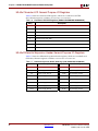
ML40x Differential Expansion Header General Purpose I/O Registers
Table 2-7 shows the differential expansion header registers, which are a standard set of
GPIO data/direction registers at address 0x90001000-0x90001004.
Table 2-7:
Bit
32
Differential Expansion Header GPIO Regs (Addr 0x90001000-0x90001004)
Description
Bit
Description
1-0
J5, Pin 4; J5, Pin 2
17-16
J5, Pin 36; J5, Pin 34
3-2
J5, Pin 8; J5, Pin 6
19-18
J5, Pin 40; J5, Pin 38
5-4
J5, Pin 12; J5, Pin 10
21-20
J5, Pin 44; J5, Pin 42
7-6
J5, Pin 16; J5, Pin 14
23-22
J5, Pin 48; J5, Pin 46
9-8
J5, Pin 20; J5, Pin 18
25-24
J5, Pin 52; J5, Pin 50
11-10
J5, Pin 24; J5, Pin 22
27-26
J5, Pin 56; J5, Pin 54
13-12
J5, Pin 28; J5, Pin 26
29-28
J5, Pin 60; J5, Pin 58
15-14
J5, Pin 32; J5, Pin 30
31-30
J5, Pin 64; J5, Pin 62
www.xilinx.com
ML40x EDK Processor Reference Design
UG082 (v5.0) June 30, 2006
R
ML40x Specific Registers
ML40x Single-Ended Expansion Header General Purpose I/O Registers
Table 2-8 shows the single-ended expansion header registers, which are a standard set of
GPIO data/direction registers at address 0x90001008-0x9000100C.
Table 2-8:
Single-Ended Expansion Header GPIO Regs (Addr 0x90001008-0x9000100C)
Bit
Description
Bit
Description
0
J6, Pin 2
16
J6, Pin 34
1
J6, Pin 4
17
J6, Pin 36
2
J6, Pin 6
18
J6, Pin 38
3
J6, Pin 8
19
J6, Pin 40
4
J6, Pin 10
20
J6, Pin 42
5
J6, Pin 12
21
J6, Pin 44
6
J6, Pin 14
22
J6, Pin 46
7
J6, Pin 16
23
J6, Pin 48
8
J6, Pin 18
24
J6, Pin 50
9
J6, Pin 20
25
J6, Pin 52
10
J6, Pin 22
26
J6, Pin 54
11
J6, Pin 24
27
J6, Pin 56
12
J6, Pin 26
28
J6, Pin 58
13
J6, Pin 28
29
J6, Pin 60
14
J6, Pin 30
30
J6, Pin 62
15
J6, Pin 32
31
J6, Pin 64
ML40x EDK Processor Reference Design
UG082 (v5.0) June 30, 2006
www.xilinx.com
33
R
Chapter 2: ML40x Embedded Processor Reference System
Extending or Modifying the Design
The ML40x Embedded Processor Reference System is a good starting point from which a
user can add, remove, or modify components in the system. Because most of the IP in the
design is attached to the CoreConnect infrastructure under EDK, adding or removing
devices is a fairly straightforward process. Below is an overview for making various
changes to the system.
Adding or Removing IP Cores
To remove an IP core:
1.
Delete the instantiation for that piece of IP from the system.mhs file (or use the
Add/Edit Cores feature of the EDK GUI).
2.
Delete all corresponding external I/O ports from the system.mhs file.
3.
Remove corresponding UCF file entries specifying timing or pinout locations for that
IP.
To add an IP core:
34
1.
Instantiate the device by adding it to the system.mhs file (or use the Add/Edit Cores
feature of the EDK GUI).
2.
Connect its external I/O to the top level.
3.
Set its configuration parameters (i.e., base address) in the system.mhs file (or use the
Add/Edit Cores feature of the EDK GUI).
4.
Add appropriate timing and pinout constraints to the UCF file.
www.xilinx.com
ML40x EDK Processor Reference Design
UG082 (v5.0) June 30, 2006
R
Chapter 3
EDK Tutorial and Demonstration
Introduction
This chapter contains basic instructions for using the EDK tools with the ML40x
Embedded Processor Reference System. It is designed to help illustrate the steps to build
and download the design. Information about demonstration software applications is also
provided. The instructions that follow provide only an overview of the capabilities of EDK.
Much more detail about operating the EDK tools can be found in the EDK documentation.
This chapter assumes that the reference design and all other necessary tools are properly
installed.
Instructions for Invoking the EDK tools
This tutorial section and those that follow have directory path names that are shown
separated by the “/” character as per the UNIX convention. For Windows, the “\” should
be used to separate directory paths.
The instructions that follow reference the <EDK Project Directory> located at:
•
ML401
♦
•
ML402
♦
•
•
MicroBlaze: <Reference Design Install Directory>/projects/ml401_emb_ref/
MicroBlaze: <Reference Design Install Directory>/projects/ml402_emb_ref/
ML403
♦
MicroBlaze: <Reference Design Install Directory>/projects/ml403_emb_ref/
♦
PPC405: <Reference Design Install Directory>/projects/ml403_emb_ref_ppc/
ML405
♦
MicroBlaze: <Reference Design Install Directory>/projects/ml405_emb_ref/
♦
PPC405: <Reference Design Install Directory>/projects/ml405_emb_ref_ppc/
These are the areas where the EDK Xilinx Microprocessor Project (XMP) files reside after
installing the ML40x Embedded Processor Reference System.
ML40x EDK Processor Reference Design
UG082 (v5.0) June 30, 2006
www.xilinx.com
35
R
Chapter 3: EDK Tutorial and Demonstration
Launching Xilinx Platform Studio (XPS)
1.
Open the XPS GUI.
On a PC, click:
Start → Programs →Xilinx Platform Studio.
On Linux, source the necessary environment scripts, and launch XPS:
$ xps
2.
Open XPS project file for the ML40x Embedded Processor Reference System:
Click File →Open Project.
Browse to find the <EDK Project Directory>.
Select the file system.xmp, click Open.
This opens the project file under EDK. It is now ready to build or download the system
using the user-selected software application program. You are now ready to proceed
with the following instructions.
Instructions for Selecting Software Application
The system.xmp EDK project file supports multiple user software applications. To select
which software application to compile, follow the instructions below.
1.
Click the Applications tab on the left-hand pane, then scroll down and look for
Project: hello_uart.
2.
Right-click on Project: hello_uart and select Make Project Active.
Note: This tutorial uses the hello_uart application as an example. To select a different software
application, right-click on the active project and select Make Project Inactive. Then find the software
application of interest and make that project active. See “Software,” page 39 for more information.
Instructions for Building and Implementing the Design
After successfully loading the design, it can now be synthesized and place-and-routed to
be run on real ML40x hardware.
1.
Synthesize the design.
In XPS, click Hardware→Generate Netlist.
Note: This step might take some time to complete.
In XPS, click Hardware→Generate Bitstream.
Note: This step might take some time to complete.
36
www.xilinx.com
ML40x EDK Processor Reference Design
UG082 (v5.0) June 30, 2006
R
Instructions for Downloading the Design
Instructions for Downloading the Design
The hardware bitstreams and software binary executable files can be downloaded to the
ML40x board using a download cable (Xilinx Parallel Cable IV or Platform Cable USB) or
the System ACE interface.
The downloaded design runs the hello_uart program. To see this program running,
connect a serial cable from a PC to the ML40x board. Use a terminal program like
HyperTerminal (shipped with Windows) and set the COM port settings to 9600 baud,
8 Data Bits, No Parity, 1 Stop Bit, No flow control. After the program is downloaded using
the instructions below, you should see Hello World! on your terminal. The board then
echoes the characters you type until you press the Escape key.
Download Using Parallel Cable IV or Platform Cable USB (iMPACT
Program)
After the design is implemented, a bitstream can be generated and downloaded into an
FPGA using a program like iMPACT, available with the Xilinx ISE tools. (A PC should be
used for this step.)
1.
Connect the download cable from a PC to the ML40x board and power on the board.
2.
Click Device Configuration → Download Bitstream within XPS.
Note: This loads a bitstream containing a bootloop program that effectively idles the processor
- not the software program that you have specified. You must continue with the remaining steps
in this section to load your program.
3.
Click Debug → Launch XMD . . .
Note: On the ML401 board, you must configure XMD to communicate with the opb_mdm
module using BSCAN number 1 instead of the default of BSCAN 0. Refer to the <EDK Project
Directory>/README file and Solution Record #20060 for more information. By default, the
ML401 xmd_microblaze_0.opt file is configured for Parallel Cable IV download and requires
editing for use with the Platform Cable USB.
Note: For ML402, ML403, and ML405, the “set the XMD Debug Options…,” message appears
the first time you run XMD. Click OK to enter debug option information such as the type of JTAG
cable you are using. Then click Save when finished. You may change debug options at any time
by selecting Debug→XMD Debug Options from the XPS GUI. Refer to the <EDK Project
Directory>/README file for more information.
4.
This opens an XMD command shell.
5.
Type into XMD:
dow microblaze_0/code/hello_uart.elf (MicroBlaze systems)
dow ppc405_0/code/hello_uart.elf (PPC405 systems)
This loads the code into memory.
6.
Type run to start the program.
ML40x EDK Processor Reference Design
UG082 (v5.0) June 30, 2006
www.xilinx.com
37
R
Chapter 3: EDK Tutorial and Demonstration
Download Using the System ACE Interface
The System ACE configuration management system allows the user to store hardware and
software information on a CompactFlash device and use it to program one or more devices
via JTAG. The ML40x platform uses the System ACE chip in conjunction with standard
CompactFlash cards to enable hardware and software programming of the FPGA. More
information about the System ACE interface is available from
http://www.xilinx.com/systemace. EDK supports the generation of System ACE files to
download bitstreams and software applications onto Virtex-4 FPGAs. This is accomplished
by concatenating (1) the JTAG commands to download the bitstream with (2) the JTAG
commands to download the software program. This combined set of JTAG commands is
encoded into an ACE file that can be read from a CompactFlash card by the System ACE
chip.
This download method creates an ACE file that contains the bitstream and software that
can be saved to the CompactFlash device and inserted into the ML40x board.
1.
Within XPS, select Device Configuration→Generate System ACE File.
Note: This command uses the local script file <EDK Project Directory>/genace.tcl (overriding the EDK
default script) to generate the ACE file <EDK Project Directory>/implementation/system.ace.
2.
Copy this file to your CompactFlash device.
-
If using a newly formatted Microdrive or CompactFlash device, copy it to the
root directory.
-
If using the CompactFlash device that shipped with ML40x, copy the ACE file
into the ML40x\myace directory of the CompactFlash device.
-
Rename the existing ACE file to system_my_ace.bak so there is only one
ACE file in the directory.
Note: On the ML402 board, it might be necessary to back up the old ACE file off the
CompactFlash device due to the limited disk space.
3.
Insert the CompactFlash device into the ML40x.
-
If the ACE file is in the root directory, it downloads immediately.
-
If the ACE file is in the ML40x\myace directory of the CompactFlash device,
select My OWN Ace File on the bootloader menu.
Refer to the System ACE and EDK documentation for further details.
38
www.xilinx.com
ML40x EDK Processor Reference Design
UG082 (v5.0) June 30, 2006
R
Software
Software
Table 3-1 (which spans multiple pages) lists the demonstration software applications
ported to the EDK design. The demonstration software is kept apart from the hardware
design to make it reusable for other projects. The user selects the desired software project
by selecting the Applications tab in the left-hand window pane and choosing which
application to use.
Table 3-1:
Demonstration Software Applications
Name
Description
Design Files
bootload
Displays menu on VGA/LCD/Serial Port and
loads appropriate ACE file based on user input.
button_led_test
Turns on LEDs when buttons are pressed.
flash_hello
Program designed to be loaded from linear flash
describing the process by which it was loaded.
sw/standalone/flash_hello/
flash_load
Program that loads data from System ACE
CompactFlash cards and programs them into
FLASH memory.
sw/standalone/flash_load/
flash_test
Program that writes and reads FLASH to test it.
sw/standalone/flash_test/
hello
Using C's studio library, prints Hello world! and
echoes characters entered via standard input to
standard output.
hello_uart
Using the EDK UART driver, prints Hello
world! on the UART and outputs characters
entered via standard input to standard output.
sw/standalone/hello_uart/
iic_eeprom
Writes test pattern to IIC and reads back data (Note:
This test will overwrite the contents of IIC only if
enabled to do so.)
sw/standalone/iic_eeprom/
my_ace
Program asking user to create their own ACE file.
sw/standalone/my_ace/
my_plat_flash
Program asking user to load their own design into
Platform Flash.
sw/standalone/my_plat_flash/
plat_flash_menu
A Program listing the demos available on the
Platform Flash. (ML401 and ML405 only.)
ps2_scancodes_polled
Polled, reads keystrokes on a keyboard attached to
PS/2 port 1 and displays corresponding PS/2
scancodes on standard output.
sw/standalone/ps2_scancodes_polled/
simon
Simon game using LCD, LEDs, and buttons on the
ML40x.
sw/standalone/simon/
slideshow
Reads audio and video files from CompactFlash via
System ACE interface and displays a slideshow
accompanied by music.
sw/standalone/slideshow/
sysace_rebooter
Program that asks user with which System ACE
configuration to reconfigure.
ML40x EDK Processor Reference Design
UG082 (v5.0) June 30, 2006
www.xilinx.com
sw/standalone/bootload/
sw/standalone/button_led_test/
sw/standalone/hello/
sw/standalone/plat_flash_menu/
sw/standalone/sysace_rebooter/
39
R
Chapter 3: EDK Tutorial and Demonstration
Table 3-1:
Demonstration Software Applications (Continued)
Name
Description
Design Files
test_ac97
Program that records sound from the LineIn/Microphone inputs, stores the audio data into
DDR memory, then plays the sound to the Line-Out
and Headphone outputs.
sw/standalone/test_ac97/
testfatfs
Simple test program that reads files from
CompactFlash via System ACE interface.
sw/standalone/testfatfs/
usb_hpi_test
Echoes characters typed on a USB keyboard to the
LCD and serial port on the ML40x.
usb_printer
Prints Hello World! to a USB printer.
sw/standalone/usb_printer
webserver
Implements a webserver that displays ML40x DIP
switch settings and controls LEDs.
sw/standalone/web_server/
xrom
ML40x board test and diagnostic program.
40
www.xilinx.com
sw/standalone/usb_hpi_test/
sw/standalone/ml40x/
sw/standalone/xrom/
ML40x EDK Processor Reference Design
UG082 (v5.0) June 30, 2006
R
Building the Linux BSP (PPC405 Systems Only)
Building the Linux BSP (PPC405 Systems Only)
The EDK design comes with MLD/TCL technology to generate a Linux BSP for ML40x
and a script to patch a MontaVista Linux kernel from the ML300 LSP for use with this BSP.
To build a BSP for and to patch the Linux kernel, proceed as follows:
1.
Start XPS and load the Linux XMP:
$ xps system_linux.xmp
2.
Generate the Linux BSP with Tools→Generate Libraries and BSPs.
The resulting Linux BSP is located in ppc405_0/libsrc/linux_mvl31_v1_00_a/linux.
3.
Quit XPS.
4.
Create a copy of the MontaVista Linux kernel for the ML300 board.
The Linux kernel and the tools to build the Linux kernel are available from MontaVista
(http://www.mvista.com).
For further information about using Linux with EDK, refer to Xilinx XAPP765: Getting
Started with EDK and MontaVista Linux.
5.
Patch the Linux kernel for use with the ML40x board:
$ cd linux
$ ./patch_linux <path to the copy of the MontaVista Linux kernel>
This step copies the .config file from the linux directory to the Linux kernel, patches
the Linux kernel with necessary changes for the ML40x board, and copies the Linux
BSP into the Linux kernel.
Build the Linux kernel.
$ cd <path to the copy of the MontaVista Linux kernel>
$ make oldconfig dep bzImage
The resulting Linux kernel resides in arch/ppc/boot/images/zImage.elf
6.
To build an ACE file consisting of the FPGA bitstream and the Linux kernel, click
Tools→Xygwin shell to run a shell, then type:
$ xmd -tcl genace.tcl -jprog -hw implementation/download.bit -elf
<Linux elf file> -ace implementation/system.ace
ML40x EDK Processor Reference Design
UG082 (v5.0) June 30, 2006
www.xilinx.com
41
R
Chapter 3: EDK Tutorial and Demonstration
42
www.xilinx.com
ML40x EDK Processor Reference Design
UG082 (v5.0) June 30, 2006
R
Chapter 4
Introduction to Hardware Reference IP
Introduction
The Embedded Processor Reference System contains additional hardware IP beyond what
is be shipped with the EDK tool suite. This hardware IP supports some of the features on
the ML40x board. The IP and its source code is provided as a reference example to
illustrate how hardware can be designed to interface with the Processor Local Bus (PLB),
On-chip Peripheral Bus (OPB), and Device Control Register (DCR) bus. Generally, the
interface and function of the IP is described, along with sufficient register information for
customers to use the devices. The reference IP source code is located within the pcores
directory of the ML40x Reference System's EDK project directory.
In addition to describing the individual hardware IPs, this document also introduces the
concept of the IP InterFace (IPIF) modules. These modules are designed to greatly
accelerate the process of connecting to pre-existent IP or creating new IP in a system. The
specification defines a CoreConnect compliant interface on one side and a simple interface
for connecting to existent IP on the other side.
The hardware IP uses the IBM CoreConnect bus standards as its means of communication
between the embedded processor and other devices. These standards are documented in
the IBM CoreConnect release. Please see the “Further Reading,” page 17 section for more
information on where to find the relevant documents.
For further information on the IPIF and each IP, see:
•
Chapter 5, “Using IPIF to Build IP”
•
Chapter 6, “OPB AC97 Sound Controller”
•
Chapter 7, “OPB PS/2 Controller (Dual)”
•
Chapter 8, “PLB TFT LCD Controller”
ML40x EDK Processor Reference Design
UG082 (v5.0) June 30, 2006
www.xilinx.com
43
R
Chapter 4: Introduction to Hardware Reference IP
Hardware Reference IP Source Format and Size
The hardware reference IP available with the ML40x Embedded Processor Reference
System originates in one language as either Verilog or VHDL source code. IP delivered in
Verilog or VHDL source format is directly viewable and editable by the user as a text file.
The EDK tools handle the process of building systems consisting of a mixture of IP written
in different languages. For example, the PLB TFT LCD Controller is available only in
Verilog source code, so the EDK tools need to convert the design into a blackbox netlist for
use in a top-level VHDL-based design.
Table 4-1 provides information about the source code format and resource utilization for
these cores. Many of the IP blocks are parameterizeable so their size might increase or
decrease depending on how they are configured. These area numbers represent a full
implementation of each IP synthesized with the Xilinx tool XST. It is important to note that
when IP is connected together in a system, logic optimizations and resource sharing can
further reduce the overall logic count. Slice utilization is only an estimate because the
packing of lookup tables (LUTs) and flip-flops (FFs) into slices depends on the overall
system implementation.
Table 4-1:
Hardware Reference IP and Logic Utilization
Source Code
Format
Name
Verilog VHDL
OPB AC97 Sound Controller
X
Logic Utilization
Slice
FFs
LUTs
Slices
(Est)
Block
RAMs
183
204
151
0
OPB PS/2 Controller
X
265
430
236
0
PLB TFT LCD Controller
X
276
289
193
1
These are all titles of individual document types in a book. Some are autonumbered, some
are not.
44
www.xilinx.com
ML40x EDK Processor Reference Design
UG082 (v5.0) June 30, 2006
R
Chapter 5
Using IPIF to Build IP
Introduction
Virtex-4 devices combine embedded processors and FPGA fabric into one integrated
circuit. In the past, system development efforts relied on engineers building each
component from scratch. Today, engineers have a wide variety of microprocessor
peripherals in their IP libraries. The Intellectual Property InterFace (IPIF) is designed to
ease the creation of new IP, as well as the integration of existent IP, within a Virtex-4 device.
This chapter illustrates the utility of the IPIF to integrate IP into a system.
The IPIF modules simplify the development of CoreConnect devices. The IPIF converts
complex system buses, such as the PLB or OPB, into common interfaces, such as an SRAM
protocol or a control register interface. This makes IPIF modules ideal for quickly
developing new bus peripherals, or converting existing IP to work in a CoreConnect busbased system. The IPIF modules provide point-to-point interfaces using simple timing
relationships and very light protocols.
The IPIF is designed to be bus-agnostic. This allows the backend interface for the IP to
remain the same while only the bus interface logic in the IPIF is changed. It, therefore,
provides an efficient means for supporting different bus standards without change to the
IP device.
IPIF modules also provide support for DMA and interrupt functionality. The IPIF is
designed to support a wide variety of common interfaces (like SRAM, FIFO, and control
register protocols). Where additional performance or functionality is required, the user can
develop a custom OPB or PLB bus interface.
IPIF modules simplify driver software development because the IPIF framework contains
many common features. These include a consistent means of interrupt handling, DMA,
and organizing control/status registers.
This document demonstrates how quickly and easily a new piece of IP can be developed
using the IPIF. The process and steps for building a new CoreConnect device based on the
SRAM protocol IPIF is described below. For this sample design, a 32-bit General Purpose
I/O (GPIO) device is created. The GPIO allows a CoreConnect master such as the CPU to
control a set of external pins using a simple memory-mapped interface.
ML40x EDK Processor Reference Design
UG082 (v5.0) June 30, 2006
www.xilinx.com
45
R
Chapter 5: Using IPIF to Build IP
SRAM Protocol Overview of IPIF
Figure 5-1 diagrams the connections between the IPIF and the user IP for SRAM protocol
interface. The IPIF simplifies the design by providing a PLB or OPB interface and
condensing it down to a small set of easily understood signals.
Bus2IP_Clk
Bus2IP_Addr[m:0]
Bus
Bus2IP_Data[0:n]
IP2Bus_Data[0:n]
Bus2IP_BE[0:b]
IP Slave
Peripheral SRAM
Module
Bus2IP_SRAM_CE
Bus2IP_WrReq
IPIF Slave
SRAM Module
IP2Bus_WrAck
Bus2IP_RdReq
IP2Bus_RdAck
Note: Supports
both with and
without DMA
IP2Bus_Retry
IP2Bus_Error
IP2Bus_ToutSup
Bus2IP_Reset
IP2Bus_Intr[0:i]
UG082_05_01_050406
Figure 5-1:
IPIF SRAM Module Interface
All interface signals with the IPIF are synchronous to rising clock edges. The IPIF takes the
clock from the OPB or PLB bus interface and passes it to the IP, causing the IP to use the
same global clock as the bus it is connected to. The SRAM interface protocol used by the
IPIF can be described by observing a write and read transaction.
46
www.xilinx.com
ML40x EDK Processor Reference Design
UG082 (v5.0) June 30, 2006
R
SRAM Protocol Overview of IPIF
Basic Write Transactions
Figure 5-2 shows the timing diagram for a write transaction. A write transaction begins
when the IPIF drives the address (Bus2IP_Addr), byte enables (Bus2IP_BE), and write data
(Bus2IP_Data) to the IP. Note that the signal direction is specified in the signal name:
Bus2IP versus IP2Bus. The IPIF qualifies the write by asserting a single clock cycle High
pulse (Bus2IP_WrReq) at the beginning of the transaction. It then waits for the IP device to
acknowledge completion of the write by sending back a single clock cycle High pulse on
IP2Bus_WrAck. During the entire transaction from Bus2IP_WrReq to IP2Bus_WrAck, the
signal Bus2IP_SRAM_CE is held high as an enveloping signal around the transaction.
After a completed transaction, the IPIF can issue a new transaction. Note that burst write
transactions on the bus are converted into a series of single data transfers to the IP, which
all look alike.
Bus2IP_Clk
Bus2IP_Addr
Valid
Valid
Bus2IP_BE
Valid
Valid
Bus2IP_Data
Valid
Valid
Bus2IP_SRAM_CE
Bus2IP_WrReq
Later Ack due
to IP response
IP2Bus_WrAck
UG082_05_02_050406
Figure 5-2:
ML40x EDK Processor Reference Design
UG082 (v5.0) June 30, 2006
IPIF Simple SRAM Write Cycle
www.xilinx.com
47
R
Chapter 5: Using IPIF to Build IP
Basic Read Transactions
Figure 5-3 diagrams a read transaction, which looks very similar to a write transaction. A
read transaction begins when the IPIF drives the address (Bus2IP_Addr) and byte enables
(Bus2IP_BE) to the IP. It qualifies the read by asserting a single clock cycle high pulse
(Bus2IP_RdReq) at the beginning of the transaction. It then waits for the IP device to
acknowledge completion of the read by sending back a single clock cycle High
acknowledge pulse on IP2Bus_RdAck. During the entire transaction from Bus2IP_RdReq
to IP2Bus_RdAck, the signal Bus2IP_SRAM_CE is held high as an enveloping signal
around the transaction. After a completed transaction, the IPIF can issue a new transaction.
Note that burst read transactions on the bus are converted into a series of single data
transfers to the IP, which all look alike.
Bus2IP_Clk
Bus2IP_Addr
Valid
Valid
Bus2IP_SRAM_CE
Bus2IP_BE
IP2Bus_Data
Valid
Valid
Valid
Valid
Bus2IP_RdReq
Later Ack due
to IP response
IP2Bus_RdAck
UG082_05_03_050406
Figure 5-3:
IPIF Simple SRAM Read Cycle
IPIF Status and Control Signals
Extra status and control signals are also present in the SRAM protocol. If the IP2Bus_Retry
signal is asserted instead of IP2Bus_RdAck/IP2Bus_WrAck, the IPIF will assert retry on
the bus side and terminate the transaction. IP2Bus_Error asserted with
IP2Bus_RdAck/IP2Bus_WrAck will cause the IPIF to signal an error on the bus interface.
For slow IP devices, an IP2Bus_ToutSup signal can be asserted to prevent timeouts on the
bus interface. Finally the Bus2IP_Reset passes the bus-side reset to the IP.
Using IPIF to Create a GPIO Peripheral from Scratch
A General Purpose Input/Output (GPIO) peripheral can be used to show how the IPIF
simplifies new peripheral creation. The GPIO module has three 32-bit registers: one
register to control the TBUF for each I/O pin, one register to write the I/O pins, and one
register to read the I/O pins. The GPIO peripheral uses a very small amount of additional
“control logic” when used with a 32-Bit IPIF Slave SRAM module.
Figure 5-4, page 49 shows a conceptual view of the logic necessary to build the GPIO
module using the IPIF Slave SRAM module. The IP2Bus_RdAck / IP2Bus_WrAck signals
are directly connected to the corresponding Bus2IP_RdReq / Bus2IP_WrReq signals, since
it only takes one clock cycle to read or write the GPIO registers. If more “access time” is
48
www.xilinx.com
ML40x EDK Processor Reference Design
UG082 (v5.0) June 30, 2006
R
Using IPIF to Create a GPIO Peripheral from Scratch
required by the registers, a simple SRL16-based shift register between the Req/Ack signals
could be used to set the number of cycles the register will respond in. An example use of
this function is to gain timing margin by treating the register access as a multicycle path.
This simple enhancement to the IPIF can have very positive effects in meeting the timing
requirements typical of complex microprocessor-based systems. Note that register
response time can be tuned differently between the read and the write.
B u s 2 I P _ Re s et
[0:7]
[ 0: 7]
Q
S
W r Re q
BE[0]
Addr[29]
D
CE
C
[8:15]
[ 8: 15]
Q
S
W r Re q
BE[1]
Addr[29]
D
CE
C
[16:23]
[ 16: 2 3]
Q
S
W r Re q
BE[2]
Addr[29]
D
CE
C
[ 2 4 : 31 ]
[ 24: 31]
Q
S
W r Re q
BE[3]
Addr[29]
D
CE
C
B u s 2 I P _ Cl k
B u s 2 I P _ A d d r [ 0 :3 1 ]
B u s 2 I P _ D a t a[ 0 : 3 1 ]
OPB
I P 2 B u s _ D a t a[ 0 :3 1 ]
Bus2IP_BE[0:3]
B u s 2 I P _ S RAM_CE
IPIF
S l ave
Module
B u s 2 I P _ W r Re q
I P 2 B u s _ W r A ck
[0:7]
T
O
[ 0: 7]
Q
W r Re q
BE[0]
Addr[29]
D
CE
C
[ 8: 15]
Q
W r Re q
BE[1]
Addr[29]
D
CE
C
[16:23]
[ 16: 2 3]
Q
I P 2 B u s _ Rd A ck
I P 2 B u s _ Re t r y
[8:15]
I
B u s 2 I P _ Rd Re q
IP2Bus_Error
I P 2 B u s _ To u t S u p
B u s 2 I P _ Re s et
W r Re q
BE[2]
Addr[29]
D
CE
C
[24:31]
[ 24: 31]
Q
W r Re q
B E [ 3]
Addr[29]
D
CE
C
[ 0 :3 1 ]
Addr[29]
1
D
Q
[ 0 :3 1 ]
0
C
U G 08 2 _ 0 5_ 0 4 _ 0 5 0 4 0 6
Figure 5-4:
IPIF SRAM Module to GPIO Logic Interface
To drive an external I/O pin, the output enable for that pin must be asserted, allowing the
pin to be driven High or Low based upon the contents of the write register. If the output
enable for a given pin is deasserted, the pin’s driver is put in a high impedance state,
allowing an external device to drive the pin. The CPU can sense the current value of any
pin (regardless of its direction) by reading the read register. Driving the direction of the
I/O pin is controlled by the contents of the three-state register.
ML40x EDK Processor Reference Design
UG082 (v5.0) June 30, 2006
www.xilinx.com
49
R
Chapter 5: Using IPIF to Build IP
The GPIO registers support byte enables during writes to the 32-bit registers. A set of
simple AND gates is all that is required to generate a clock enable to the registers. Four
3-input AND gates are used to drive the four bytes of the three-state control register, and
four more 3-input AND gates are used to drive the four bytes of output-pin data.
The IPIF uses a set of user-specified parameters that allow common things, such as the base
address of the IP, to be established. These parameters are specified before the system is
implemented in order to minimize the logic area and maximize the performance of the
system. Note that in the GPIO example, additional decoding is used externally to specify
two different memory locations. One location is used for reading from or writing to the
I/O pins (read register and write register share the same address), and one location is used
for 3-state control, reading and writing to the bit that controls the T of the I/O pins.
Using IPIF to Connect a Pre-Existent Peripheral to the Bus
Often, some legacy IP needs to be brought into a modern system. Many of these legacy IPs
use some form of an 8-bit microprocessor bus. Typically, this might consist of a few address
lines, an 8-bit data bus, a read and write signal, a chip enable, a clock, a reset, and perhaps
an interrupt pin. In most instances, this kind of IP can be almost directly connected to the
IPIF SRAM module. This particular IPIF module was actually designed to serve this very
purpose.
To connect a legacy IP, simply connect the address, data, chip enable, clock, reset, and
interrupt pins to their corresponding versions in the IPIF SRAM module. Some small
amount of logic might be needed to generate a properly timed read or write signal. The
IPIF SRAM module provides separate Req/Ack pairs for read and write, because many
older peripherals require different timing for reads and writes. For read or write, the logic
between the IP and the IPIF must accomplish two things:
•
Provide the proper response time to the IPIF so the peripheral’s register can be read or
written
•
Provide the proper relationship of the read or write signal on the IP relative to the
address and data
Consider the following example: The IP might expect its write signal to be valid one clock
after address and data is valid and be held for four clock cycles to properly write the data.
After write goes invalid, the address and data must be held for one additional cycle. To
accommodate this kind of pattern, a six-stage shift register (SR) can be implemented. The D
input to the SR is tied to the Bus2IP_WrReq pin, and the Q output of the SR is tied to the
IP2Bus_WrAck pin of the IPIF. This provides the proper timing for the length of time the
cycle must be held on the bus. By using the first, second, third, and fourth taps of the SR,
and feeding them into an OR gate, a write strobe can be generated for the IP. If this write
strobe must be glitch-free, taps 0, 1, 2, and 3 could be used, OR’ed, and fed into a
synchronizing register. Xilinx FPGAs are abundantly equipped with flip-flops, so the
amount of logic is not an issue.
50
www.xilinx.com
ML40x EDK Processor Reference Design
UG082 (v5.0) June 30, 2006
R
Conclusion
Conclusion
Using the IPIF with a small amount of logic makes it very easy to create CoreConnect
devices with little knowledge of the buses used. For complex buses such as PLB, this saves
the designer time and helps to ensure IP functions correctly, since the IPIF provides a preverified design to connect to. The GPIO design is just one example of how IPIF can be used.
More examples of IPIF designs are provided within many of the other IP devices in the
reference systems. The designer who wants to learn about IPIF should study the sample
source code for some of these IPIF-based designs in context with simulation to gain
experience with IPIF.
The IPIF used in the ML40x Embedded Processor Reference System currently supports
only the SRAM module. Additional IPIF modules are available through EDK that support
many parameterizeable features. Refer to the IPIF chapter of the Processor IP Reference
Guide located in <EDK Install Directory>/doc/proc_ip_ref_guide.pdf.
Note: The Hardware Reference IP in the following chapters are built using IPIF modules conforming
to an earlier version of the specification. Please refer to the IPIF chapter of the Processor IP
Reference Guide (located in <EDK Install Directory>/doc/proc_ip_ref_guide.pdf) for the latest
information and documentation on IPIF cores. New designs should use these IPIF modules, available
through EDK. For reference, the earlier version of the IPIF spec is available in Chapter 6 of Xilinx
UG057: ML300 EDK Reference Design User Guide.
ML40x EDK Processor Reference Design
UG082 (v5.0) June 30, 2006
www.xilinx.com
51
R
Chapter 5: Using IPIF to Build IP
52
www.xilinx.com
ML40x EDK Processor Reference Design
UG082 (v5.0) June 30, 2006
R
Chapter 6
OPB AC97 Sound Controller
Overview
This module is an On-Chip Peripheral Bus (OPB) slave device that is designed to control an
AC97 Audio Codec chip. It provides a simple memory-mapped interface to communicate
with the high-speed serial ports of the AC97 Codec. The OPB AC97 Sound Controller
module allows full access to all control and status registers in the AC97 chip and provides
data buffering for stereo playback and recording.
Related Documents
The following documents provide additional information:
•
IBM CoreConnect 64-Bit On-Chip Peripheral Bus: Architecture Specifications, V2.1
•
Virtex-4 Platform FPGAs (Data Sheets)
•
Intel Audio Codec '97 (AC97) Specification
http://www.intel.com/technology/computing/audio/index.htm
•
16-deep FIFO buffer for record and playback data
•
Capable of generating interrupts when play/record FIFOs reach given fullness
thresholds
Features
ML40x EDK Processor Reference Design
UG082 (v5.0) June 30, 2006
www.xilinx.com
53
R
Chapter 6: OPB AC97 Sound Controller
Module Port Interface
Information about the signals, pins, and parameters for the module is listed in tables
Table 6-1, Table 6-2, Table 6-3, Table 6-4, page 55.
Table 6-1:
Global Signals
Name
Direction
OPB_Clk
Input
OPB system clock
OPB_Rst
Input
OPB system reset
Table 6-2:
OPB Slave Signals
Name
Direction
Description
OPB_ABus[0:31]
Input
OPB address bus
OPB_BE[0:3]
Input
OPB byte enables
OPB_DBus[0:31]
Input
OPB data bus
OPB_RNW
Input
OPB read-not-write
OPB_select
Input
OPB select
OPB_seqAddr
Input
OPB sequential address
OPB_AC97_CONTROLLER_DBus[0:31]
Output
Slave data bus
OPB_AC97_CONTROLLER_errAck
Output
Slave error acknowledge
OPB_AC97_CONTROLLER_retry
Output
Slave bus cycle retry
OPB_AC97_CONTROLLER_toutSup
Output
Slave time-out suppress
OPB_AC97_CONTROLLER_xferAck
Output
Slave transfer acknowledge
Table 6-3:
External I/O Pins
Name
Direction
Description
Playback_Interrupt
Output
Interrupt generated when play buffer fullness is
at or below programmed threshold.
Record_Interrupt
Output
Interrupt generated when record buffer fullness
is at or above programmed threshold.
Bit_Clk
Input
Serial Bit Clock from AC97 Codec.
Sync
Output
Frame synchronization signal to AC97 Codec.
SData_Out
Output
Serial Data output to AC97 Codec.
SData_In
54
Description
Input
www.xilinx.com
Serial Data input from AC97 Codec.
ML40x EDK Processor Reference Design
UG082 (v5.0) June 30, 2006
R
Module Port Interface
Table 6-4:
Generics (Parameters)
Name
Default
Description
C_OPB_AWIDTH
32
Address bus width of OPB. Should be set to 32.
C_OPB_DWIDTH
32
Data bus width of OPB. Should be set to 32.
C_BASEADDR
N/A
Base Address of AC97 Sound Controller. Should be
set to 256-byte (or higher power of 2) boundary.
C_HIGHADDR
N/A
End Address of AC97 Sound Controller. Should be
set to (Base Address + 0xFF) or higher. Total memory
space from C_BASEADDR to C_HIGHADDR must
be power of 2.
C_PLAYBACK
1
Playback Enable. Set to 1 to allow playback. Set to 0
to remove playback logic.
C_RECORD
1
Record Enable. Set to 1 to allow record. Set to 0 to
remove record logic.
C_PLAY_INTR_LEVEL
2
Sets playback FIFO fullness threshold at which
interrupt is generated:
0 = No Interrupt
1 = empty
Num Words = 0
2 = halfempty Num Words <= 7
3 = halffull
Num Words >= 8
4 = full
Num Words = 16
C_REC_INTR_LEVEL
3
Sets record FIFO fullness threshold at which
interrupt is generated:
0 = No Interrupt
1 = empty
Num Words = 0
2 = halfempty Num Words <= 7
3 = halffull
Num Words >= 8
4 = full
Num Words = 16
ML40x EDK Processor Reference Design
UG082 (v5.0) June 30, 2006
www.xilinx.com
55
R
Chapter 6: OPB AC97 Sound Controller
Implementation
Figure 6-1, page 56 shows a block diagram of the OPB AC97 Sound Controller. The OPB
AC97 Sound Controller module manages three primary functions to control the AC97
Codec chip. It handles the playback FIFO, record FIFO, and the Codec's control/status
registers.
OPB AC97 Sound Controller
SData_Out
Serial
to
Parallel
16
Parallel
to
Serial
Parallel
to
Serial
Serial
to
Parallel
16
Codec Data
Playback FIFO
16
Record FIFO
7
Q
D
Q
D
16
16
D
Q
AC97 Clock Domain
7
Address
16
Write Data
OPB Interface Logic
AC97
Codec
AC97 Interface Logic
SData_In
16
Codec Control/Status
Register
M
U
X
Parallel
to
Serial
OPB
16 Read Data
OPB Clock Domain
UG082_06_01_050406
Figure 6-1: OPB AC97 Sound Controller Block Diagram
The playback FIFO is a 16-word deep x 16-bit wide FIFO. The playback data is stored by
alternating between left and right channel data (beginning with the left channel). This
allows the 16-entry FIFO to store a total of eight stereo data samples. Software should be
interrupt driven and programmed to refill the playback FIFO after an interrupt is received
stating that the FIFO is nearly empty. If operating in polled mode, the software should poll
the playback FIFO-full status bit and refill the FIFO when it is not full. If the playback FIFO
goes into an underrun condition (FIFO is empty and Codec requests more data), an error
flag bit is set. If the playback FIFO is underrun, the FIFO must be reset to clear the error flag
and to ensure proper operation. The FIFO threshold at which an interrupt is generated can
be set to one of four possible fullness levels. The OPB AC97 controller logic automatically
handles the process of serializing the left/right playback data and sending it out to the
Codec chip when requested.
56
www.xilinx.com
ML40x EDK Processor Reference Design
UG082 (v5.0) June 30, 2006
R
Memory Map
The record FIFO is a 16-word deep x 16-bit wide FIFO. The record data is stored in an
alternating fashion between left and right channel data (beginning with the left channel).
This allows the 16-entry FIFO to store a total of eight stereo data samples. Software should
be interrupt driven and programmed to empty the record FIFO after an interrupt is
received stating that the FIFO is nearly full. If operating in polled mode, the software
should poll the playback FIFO-empty status bit and get data from the FIFO when it is not
empty. If the record FIFO goes into an overrun condition (FIFO is full and Codec sends
more data), an error flag bit is set. If the record FIFO is overrun, the FIFO must be reset to
clear the error flag and to ensure proper operation. The FIFO threshold at which an
interrupt is generated can be set to one of four possible emptiness levels. The OPB AC97
controller logic automatically handles the process of parallelizing the left/right serial
record data that is received from the Codec chip.
The playback and record FIFOs must be operated with the same sampling frequency
between the left and right channels. The FIFO logic does not support the left and right
channels operating at different frequencies.
Access to the control/status registers in the Codec chip is performed through a set of
keyhole registers. To write to the control registers in the Codec chip, the write data and
then the address to be accessed are written to two registers in the OPB AC97 controller.
This causes the write data to be serialized and sent to the Codec chip. A status bit signals
when the write is complete. Reading a status register in the Codec chip is performed in a
similar manner. The read address is written to the OPB AC97 controller. This causes a read
command to be serialized and sent to the Codec chip. When the Codec chip responds with
the read data, a status bit is set indicating that the return data is available. See the “Memory
Map” section for more information about using these registers.
The Bit_Clk from the AC97 Codec chip typically runs at a frequency of 12.288 MHz while
the OPB clock runs with a typical frequency of 50-100 MHz. Because of the asynchronous
relationship between these two clock domains, the OPB AC97 controller contains special
logic to pass data between these two clock domains. In order for this synchronizing logic to
function properly, it is important that the OPB clock frequency is at least two times higher
than the AC97 Bit_Clk frequency.
Memory Map
Information about the memory mapped registers is shown in Table 6-5 (which spans
multiple pages).
Table 6-5:
Memory Map
Bits
Read/
Write
Base Address + 0
[16:31]
W
Write 16-bit data sample to playback FIFO. Data
should be written two at a time to write data to the
left channel followed by the right channel.
Base Address + 4
[16:31]
R
Read 16-bit data sample from record FIFO. Data
should be read two at a time to get data from the left
channel followed by the right channel.
Register Address
ML40x EDK Processor Reference Design
UG082 (v5.0) June 30, 2006
www.xilinx.com
Description
57
R
Chapter 6: OPB AC97 Sound Controller
Table 6-5:
Memory Map (Continued)
Register Address
Bits
Read/
Write
Base Address + 8
[24]
R
Description
Record FIFO Overrun:
0 = FIFO has not overrun
1 = FIFO has overrun
Note: Record FIFO must be reset to clear this
bit. After an overrun has occurred, the Record
FIFO will not operate properly until it is reset.
[25]
R
Play FIFO Underrun:
0 = FIFO has not underrun
1 = FIFO has underrun
Note: Play FIFO must be reset to clear this bit.
After an underrun has occurred, the Play FIFO
will not operate properly until it is reset.
[26]
R
Codec Ready:
0 = Codec is not ready to receive commands or
data. (This can occur during initial power-on or
immediately after reset.)
1 = Codec ready to run
[27]
R
Register Access Finish:
0 = AC97 Controller waiting for access to
control/status register in Codec to complete.
1 = AC97 Controller is finished accessing the
control/status register in Codec.
Note: This bit is cleared when there is a write
to the "AC97 Control Address Register"
(described below).
[28]
R
Record FIFO Empty:
0 = Record FIFO not Empty
1 = Record FIFO Empty
[29]
R
Record FIFO Full:
0 = Record FIFO not Full
1 = Record FIFO Full
[30]
R
Playback FIFO Half Full:
0 = Playback FIFO not Half Full
1 = Playback FIFO Half Full
[31]
(LSB)
58
R
www.xilinx.com
Playback FIFO Full:
0 = Playback FIFO not Full
1 = Playback FIFO Full
ML40x EDK Processor Reference Design
UG082 (v5.0) June 30, 2006
R
Memory Map
Table 6-5:
Memory Map (Continued)
Register Address
Bits
Read/
Write
Base Address + 12
[30]
W
Description
Clear/Reset Record FIFO:
0 = Do not Reset Record FIFO
1 = Reset Record FIFO. Resetting the record FIFO
also clears the "Record FIFO Overrun" status bit.
[31]
W
Clear/Reset Play FIFO:
0 = Do not Reset Play FIFO
1 = Reset Play FIFO. Resetting the Play FIFO also
clears the "Play FIFO Underrun" status bit.
Base Address + 16
[24:30]
W
AC97 Control Address Register:
Sets the 7-bit address of control or status register
in the Codec chip to be accessed. Writing to this
register clears the "Register Access Finish" status
bit.
[31]
W
AC97 Control Address Register:
0 = Perform a write to the address specified
above. The write data comes from the "AC97
Control Data Write Register" which should be set
beforehand.
1 = Performs a read to the address above. Writing
to this register clears the "Register Access Finish"
status bit. This bit is asserted high when the
operation is complete.
Base Address + 20
[24:31]
R
AC97 Status Data Read Register:
Returns data from the status register in the Codec
that was read by the command above. Data is
valid when the "Register Access Finish" flag is
set.
Base Address + 24
[24:31]
W
AC97 Control Data Write Register:
Contains the data to be written to the control
register in the Codec. This register is used in
conjunction with the "AC97 Control Address
Register" described above.
ML40x EDK Processor Reference Design
UG082 (v5.0) June 30, 2006
www.xilinx.com
59
R
Chapter 6: OPB AC97 Sound Controller
60
www.xilinx.com
ML40x EDK Processor Reference Design
UG082 (v5.0) June 30, 2006
R
Chapter 7
OPB PS/2 Controller (Dual)
Overview
This module is an On-Chip Peripheral Bus (OPB) slave device that is designed to control
two PS/2 devices such as a mouse and keyboard. It utilizes the Xilinx Intellectual Property
InterFace (IPIF) to simplify its design. The OPB PS/2 Controller module generates
interrupts upon various transmit or receive conditions. This document assumes the user is
already familiar with the PS/2 interface protocol. Additional information about PS/2 ports
and peripherals is widely available on the Internet or through a computer hardware
reference manual.
Related Documents
The following documents provide additional information:
•
IPIF Specification
•
IBM CoreConnect 64-Bit On-Chip Peripheral Bus: Architecture Specifications, V2.1
•
Virtex-4 Platform FPGAs (Data Sheets)
•
32-bit OPB slave utilizing a 32-bit IPIF Slave SRAM interface
•
Implements 8-bit read/write interface found in many PCs to control each PS/2 port
Features
ML40x EDK Processor Reference Design
UG082 (v5.0) June 30, 2006
www.xilinx.com
61
R
Chapter 7: OPB PS/2 Controller (Dual)
Module Port Interface
Information about the signals, pins, and parameters for the module is listed in tables
Table 7-1, Table 7-2, and Table 7-3, page 63.
Table 7-1:
OPB Slave Signals
Name
Description
IPIF_Rst
Input
OPB system reset
OPB_BE[0:3]
Input
OPB byte enables
OPB_Select
Input
OPB select
OPB_Dbus[0:31]
Input
OPB data bus
OPB_Clk
Input
OPB system clock
OPB_Abus[0:31]
Input
OPB address bus
OPB_RNW
Input
OPB read not write
OPB_seqAddr
Input
OPB sequential address
Sln_XferAck
Output
Slave transfer acknowledge
Sln_Dbus[0:31]
Output
Slave data bus
Sln_DBusEn
Output
Slave data bus enable
Sln_errAck
Output
Slave error acknowledge
Sln_retry
Output
Slave bus cycle retry
Sln_toutSup
Output
Slave timeout suppress
Table 7-2:
External I/O Pins
Name
Sys_Intr1
Direction
Output
Clkin1
Input
Clkpd1
Output
Rx1
Input
Description
Interrupt, Port #1
PS/2 Clock In, Port #1
PS/2 Clock Pulldown, Port #1
PS/2 Serial Data In, Port #1
Txpd1
Output
PS/2 Serial Data Out Pulldown, Port #1
Sys_Intr2
Output
Interrupt, Port #2
Clkin2
Input
Clkpd2
Output
Rx2
Txpd2
62
Direction
Input
Output
www.xilinx.com
PS/2 Clock In, Port #2
PS/2 Clock Pulldown, Port #2
PS/2 Serial Data In, Port #2
PS/2 Serial Data Out Pulldown, Port #2
ML40x EDK Processor Reference Design
UG082 (v5.0) June 30, 2006
R
Module Port Interface
Table 7-3:
Parameters
Name
Description
C_BASEADDR
32-bit base address of PS/2 controller (must be aligned to 8-KB
boundary)
C_HIGHADDR
Upper address boundary, must be set to value of
C_BASEADDR + 0x1FFF (8-KB boundary)
ML40x EDK Processor Reference Design
UG082 (v5.0) June 30, 2006
www.xilinx.com
63
R
Chapter 7: OPB PS/2 Controller (Dual)
Implementation
Figure 7-1 shows a block diagram of the OPB PS/2 Controller module. It uses an IPIF slave
with an SRAM interface in addition to simple state machines and shift registers to
implement its functionality. Each PS/2 port is controlled by a separate set of eight bytewide registers.
For transmitting data, a byte write to the transmit register causes that data to be serialized
and sent to the PS/2 device. Status registers and interrupts then signal when the
transmission is complete and if there are any errors reported. Similarly, receiver status
registers and interrupts signal when data has been received from the PS/2 device. Any
errors with received data are also reported.
The PS/2 controller can be operated in a polled mode or an interrupt driven mode. In the
interrupt driven mode, separate register bits for setting, clearing, and masking of
individual interrupts are provided.
Because the PS/2 interface uses an open collector circuit for transmitting data, the output
signals Clkpd and Txpd should be tied to a transistor or logic gate capable of pulling the
5V PS/2 clock and data signals low. Note that the PS/2 protocol specifies 5V signalling.
Therefore, it is necessary to have the proper interface circuitry to prevent over-voltage
conditions on the FPGA I/O. Consult the schematics and documentation for the Xilinx
ML40x board for an example implementation of a PS/2 port interface circuit.
OPB
Misc control logic
PS2_1_DATA_OUT
Memory
Mapped
Registers
TX State Machine
Shift
Registers
and
Clock
Controls
PS2_1_DATA_IN
PS2_1_CLK_OUT
PS2_1_CLK_IN
ps2_reg.v
RX State Machine
ps2_sie.v
OPB
Slave
IPIF
Misc control logic
PS2_2_DATA_OUT
Memory
Mapped
Registers
TX State Machine
Shift
Registers
and
Clock
Controls
PS2_2_DATA_IN
PS2_2_CLK_OUT
PS2_2_CLK_IN
ps2_reg.v
RX State Machine
ps2_sie.v
UG082_07_01_050406
Figure 7-1: OPB PS/2 Controller Block Diagram
64
www.xilinx.com
ML40x EDK Processor Reference Design
UG082 (v5.0) June 30, 2006
R
Memory Map
Memory Map
Information about the memory mapped registers is shown in Table 7-4.
Note:
Table 7-4:
1.
Control/status registers for PS/2 Port #1 start at the base address
(value of parameter C_BASEADDR).
2.
Control/status registers for PS/2 Port #2 start at the base address + 0x1000
(value of parameter C_BASEADDR + 0x1000).
Memory Map Table
Offset
Bit
0
Bit
1
Bit
2
Bit
3
Bit
4
Bit
5
Bit
6
x00
Reserved
x04
Reserved
x08
RXR
R*
x0c
TXR
R*
x10
Reserved
INSTA.2
rx_full
INSTA.3
rx_err
INSTA.4
rx_ovf
INSTA.5
tx_ackf
INSTA.6
tx_noack
INSTA.7
wdt_tout
R*
x14
Reserved
INTCLR.2
rx_full
INTCLR.3
rx_err
INTCLR.4
rx_ovf
INTCLR.5
tx_ackf
INTCLR.6
tx_noack
INTCLR.7
wdt_tout
R*
x18
Reserved
INTMSET.2
rx_full
INTMSET.3
rx_err
INTMSET.4
rx_ovf
INTMSET.5
tx_ackf
INTMSET.6
tx_noack
INTMSET.7
wdt_tout
R*
x1c
Reserved
INTMCLR.2
rx_full
INTMCLR.3
rx_err
INTMCLR.4
rx_ovf
INTMCLR.5
tx_ackf
INTMCLR.6
tx_noack
INTMCLR.7
wdt_tout
R*
STR.6
tx_full_sta
Bit
7
Bit
8-31
SRST
R*
STR.7
rx_full_sta
R*
* R = Reserved
All fields marked Reserved return zero. The field in INTSTA(x10) is AND'ed with the fields
in INTM(x18), then the bits get OR'ed to form a single Interrupt signal.
The register pairs INTSTA/INTCLR and INTMSET/INTMCLR are implemented to allow
single bit register updates which reduce the latency of interrupt handling. INTCLR and
INTMCLR are helper functions that make setting and clearing the Interrupt Status Register
and Interrupt Mask Register faster.
The register definitions are shown in Table 7-5, page 66 (this table spans several pages).
Note: The second PS/2 Port has an identical set of control/status registers at an additional offset of
0x1000.
ML40x EDK Processor Reference Design
UG082 (v5.0) June 30, 2006
www.xilinx.com
65
R
Chapter 7: OPB PS/2 Controller (Dual)
Table 7-5:
OPB PS/2 Slave Device Pin Description
Name
Field Name
Bit
Direction
7
W
Base Address + 0
(Offset x00)
SRST
Base Address + 4
(Offset x04)
STR.6
tx_full_sta
6
STR.7
rx_full_sta
7
Description
Software Reset.
Writing '1' into this register results in the PS/2 controller
being reset to idle state. Also, registers at offset x04, x10, x14
will be reset by this bit as well.
R
TX Register Full.
PS/2 Serial Interface Engine is busy. This register can only be
modified by PS/2 SIE hardware. Software does not have
direct write permission to change this field because this field
is set by the state machine in the SIE. Software can clear this
field indirectly is by using the SRST register.
R
RX Register Full.
PS/2 Serial Interface Engine received a byte package. The
associated interrupt “rx_full” (INTSTA.3) will also be set.
Software does not have direct write permission to change
this field since this field is set by the state machine in the SIE.
Software can clear this field indirectly is by using the SRST
register.
Base Address + 8
(Offset x08)
RXR
[0:7]
R
RX received data.
Base Address + 12
(Offset x0c)
TXR
[0:7]
W
TX transmission data.
66
www.xilinx.com
ML40x EDK Processor Reference Design
UG082 (v5.0) June 30, 2006
R
Table 7-5:
Memory Map
OPB PS/2 Slave Device Pin Description (Continued)
Name
Base Address + 16
(Offset x10)
Field Name
Bit
Direction
INSTA.2
rx_full
2
R
INSTA.3
rx_err
3
INSTA.4
rx_ovf
4
INSTA.5
tx_ackf
5
INSTA.6
tx_noack
6
INSTA.7
wdt_tout
7
ML40x EDK Processor Reference Design
UG082 (v5.0) June 30, 2006
Description
Interrupt Status Register - RX data register full.
This field is updated by the PS/2 Serial Interface when the
SIE has received a data packet. Software clears this field by
writing a '1' into the corresponding interrupt clear register
INTCLR.2 (offset x14.2)
R
Interrupt Status Register - RX data error.
This field is updated by the PS/2 Serial Interface when the
SIE has found that RX data is a bad packet. Software clears
this field by writing a '1' into the corresponding interrupt
clear register INTCLR.3 (offset x14.3)
R
Interrupt Status Register - RX data register overflow.
This field is updated by the PS/2 Serial Interface when the
SIE overwrites a data packet before the previous data was
read. Software clears this field by writing a '1' into the
corresponding interrupt clear register INTCLR.4 (offset
x14.4)
R
Interrupt Status Register - TX acknowledge received.
This field is updated by the PS/2 Serial Interface when the
SIE completes transmission of a data byte and has received
acknowledgement from the PS/2 device.Software clears this
field by writing an '1' into the corresponding interrupt clear
register INTCLR.5 (offset x14.5)
R
Interrupt Status Register - TX acknowledge not received.
This field is updated by the PS/2 Serial Interface when the
SIE completes transmission of a data byte but has not yet
received acknowledgement from the PS/2 device.Software
clears this field by writing an '1' into the corresponding
interrupt clear register INTCLR.6 (offset x14.6)
R
Interrupt Status Register - Watch dog timer timeout.
This field is updated by the PS/2 Serial Interface when the
SIE does not receive a PS/2 Clock while a packet is still being
transmitted. Software clears this field by writing an '1' into
the corresponding interrupt clear register INTCLR.7 (offset
x14.7)
www.xilinx.com
67
R
Chapter 7: OPB PS/2 Controller (Dual)
Table 7-5:
OPB PS/2 Slave Device Pin Description (Continued)
Name
Base Address + 20
(Offset x14)
Field Name
Bit
Direction
INTCLR.2
rx_full
2
R*/W
INTCLR.3
rx_err
3
INTCLR.4
rx_ovfl
4
INTCLR.5
tx_ack
5
INTCLR.6
tx_noak
6
INTCLR.7
wdt_toutl
7
Description
Interrupt Clear Register - RX data register full.
Writing a '1' to this field clears INTSTA.2.
Writing a '0' has no effect.
R*/W
Interrupt Clear Register - RX data error.
Writing a '1' to this field clears INTSTA.3.
Writing a '0' has no effect.
R*/W
Interrupt Clear Register - RX data register overflow.
Writing a '1' to this field clears INTSTA.4.
Writing a '0' has no effect.
R*/W
Interrupt Clear Register - TX acknowledge received.
Writing a '1' to this field clears INTSTA.5.
Writing a '0' has no effect.
R*/W
Interrupt Clear Register - TX acknowledge not received.
Writing a '1' to this field clears INTSTA.6.
Writing a '0' has no effect.
R*/W
Interrupt Clear Register - Watch dog timer timeout.
Writing a '1' to this field clears INTSTA.7.
Writing a '0' has no effect.
* If software tries to read from INTCLR (offset x14), the value of INTSTA (offset x10) is returned.
Base Address + 24
(Offset x18)
INTMSET.2
rx_full
2
R*/W
INTMSET.3
rx_err
3
R*/W
INTMSET.4
rx_ovf
4
INTMSET.5
tx_ack
5
INTMSET.6
tx_noack
6
INTMSET.7
wdt_tout
7
Interrupt Mask Set Register - RX data register full. Writing a
'1' to this field sets INTM.2.
Writing a '0' has no effect.
Interrupt Mask Set Register - RX data error.
Writing a '1' to this field sets INTM.3.
Writing a '0' has no effect.
R*/W
Interrupt Mask Set Register - RX data register overflow.
Writing a '1' to this field sets INTM.4.
Writing a '0' has no effect.
R*/W
Interrupt Mask Set Register - TX acknowledge received.
Writing a '1' to this field sets INTM.5.
Writing a '0' has no effect.
R*/W
Interrupt Mask Set Register - TX acknowledge not received.
Writing a '1' to this field sets INTM.6.
Writing a '0' has no effect.
R*/W
Interrupt Mask Set Register - Watch dog timer timeout.
Writing a '1' to this field sets INTM.7.
Writing a '0' has no effect.
* If software tries to read from INTMSET (offset x18), the value of INTM register is returned.
68
www.xilinx.com
ML40x EDK Processor Reference Design
UG082 (v5.0) June 30, 2006
R
Table 7-5:
Memory Map
OPB PS/2 Slave Device Pin Description (Continued)
Name
Base Address + 28
(Offset x1C)
Field Name
Bit
Direction
INTMCLR.2
rx_full
2
R*/W
INTMCLR.3
rx_err
3
INTMCLR.4
rx_ovf
4
INTMCLR.5
rx_ack
5
INTMCLR.6
rx_noack
6
Description
Interrupt Mask Clear Register - RX data register full.
Writing a '1' to this field clears INTM.2.
Writing a '0' has no effect.
R*/W
Interrupt Mask Clear Register - RX data error.
Writing a '1' to this field clears INTM.3.
Writing a '0' has no effect.
R*/W
Interrupt Mask Clear Register - RX data register overflow.
Writing a '1' to this field clears INTM.4.
Writing a '0' has no effect.
R*/W
Interrupt Mask Clear Register - TX acknowledge received.
Writing a '1' to this field clears INTM.5.
Writing a '0' has no effect
R*/W
Interrupt Mask Clear Register - TX acknowledge not
received.
Writing a '1' to this field clears INTM.6.
Writing a '0' has no effect.
INTMCLR.7
wdt_tout
7
R*/W
Interrupt Mask Clear Register - Watch dog timer timeout.
Writing a '1' to this field clears INTM.7.
Writing a '0' has no effect.
* If software tries to read from IINTMCLR (offset x1C), the value of INTM (offset x18) is returned.
ML40x EDK Processor Reference Design
UG082 (v5.0) June 30, 2006
www.xilinx.com
69
R
Chapter 7: OPB PS/2 Controller (Dual)
70
www.xilinx.com
ML40x EDK Processor Reference Design
UG082 (v5.0) June 30, 2006
R
Chapter 8
PLB TFT LCD Controller
Overview
The PLB TFT LCD Controller is a hardware display controller for a 640x480 resolution TFT
or VGA screen. It is capable of showing up to 256K colors and is designed for a TFT
display, but can also be used for the VGA port on the Xilinx ML40x board. The design
contains a PLB master interface that reads video data from a PLB attached memory device
(not part of this design) and displays the data onto the TFT screen. The design also contains
a Device Control Register (DCR) interface used for configuring the controller.
Related Documents
The following documents provide additional information
•
IBM CoreConnect 32-Bit Device Control Register Bus: Architecture Specifications
•
IBM CoreConnect 64-Bit Processor Local Bus: Architecture Specification
•
Virtex-4 Platform FPGAs (Data Sheets)
•
32-bit DCR slave interface for control registers
•
64-bit PLB master interface for fetching pixel data
•
Support for asynchronous PLB and TFT clocks
Features
Module Port Interface
Information about the signals, pins, and parameters for the module is listed in Table 8-1,
Table 8-2, page 72, Table 8-3, page 73, Table 8-4, page 73, and Table 8-5, page 74.
Table 8-1:
Global Signals
Name
Direction
Description
SYS_dcrClk
Input
DCR System Clock
SYS_plbClk
Input
PLB System Clock
SYS_plbReset
Input
PLB System Reset
SYS_tftClk
Input
TFT Video Clock
ML40x EDK Processor Reference Design
UG082 (v5.0) June 30, 2006
www.xilinx.com
71
R
Chapter 8: PLB TFT LCD Controller
Table 8-2:
PLB Master Signals
Name
72
Direction
Description
PLB_MnAddrAck
Input
PLB master address acknowledge
PLB_MnBusy
Input
PLB master slave busy indicator
PLB_MnErr
Input
PLB master slave error indicator
PLB_MnRdBTerm
Input
PLB master terminate read burst indicator
PLB_MnRdDAck
Input
PLB master read data acknowledge
PLB_MnRdDBus[0:63]
Input
PLB master read data bus
PLB_MnRdWdAddr[0:3]
Input
PLB master read word address
PLB_MnRearbitrate
Input
PLB master bus rearbitrate indicator
PLB_Mnssize[0:1]
Input
PLB slave data bus size
PLB_MnWrBTerm
Input
PLB master terminate write burst indicator
PLB_MnWrDAck
Input
PLB master write data acknowledge
PLB_pendPri[0:1]
Input
PLB pending request priority
PLB_pendReq
Input
PLB pending bus request indicator
PLB_reqPri[0:1]
Input
PLB current request priority
Mn_abort
Output
Master abort bus request indicator
Mn_ABus[0:31]
Output
Master address bus
Mn_BE[0:7]
Output
Master byte enables
Mn_busLock
Output
Master bus lock
Mn_compress
Output
Master compressed data transfer indicator
Mn_guarded
Output
Master guarded transfer indicator
Mn_lockErr
Output
Master lock error indicator
Mn_msize[0:1]
Output
Master data bus size
Mn_ordered
Output
Master synchronize transfer indicator
Mn_priority[0:1]
Output
Master bus request priority
Mn_rdBurst
Output
Master burst read transfer indicator
Mn_request
Output
Master bus request
Mn_RNW
Output
Master read/not write
Mn_size[0:3]
Output
Master transfer size
Mn_type[0:2]
Output
Master transfer type
Mn_wrBurst
Output
Master burst write transfer indicator
Mn_wrDBus[0:63]
Output
Master write data bus
www.xilinx.com
ML40x EDK Processor Reference Design
UG082 (v5.0) June 30, 2006
R
Module Port Interface
Table 8-3:
DCR Slave Signals
Name
Direction
Description
DCR_ABus[0:9]
Input
DCR Address Bus
DCR_DBusIn[0:31]
Input
DCR Data Bus In
DCR_Read
Input
DCR Read Strobe
DCR_Write
Input
DCR Write Strobe
DCR_Ack
Output
DCR Acknowledge
DCR_DBusOut[0:31]
Output
DCR Data Bus Out
Table 8-4:
External Output Pins
Name
Direction
Description
TFT_LCD_HSYNC
Output
Horizontal Sync (Negative Polarity)
TFT_LCD_VSYNC
Output
Vertical Sync (Negative Polarity)
TFT_LCD_DE
Output
Data Enable
TFT_LCD_CLK
Output
Video Clock
TFT_LCD_DPS
Output
Selection of Scan Direction
TFT_LCD_R[5:0]
Output
Red Pixel Data
TFT_LCD_G[5:0]
Output
Green Pixel Data
TFT_LCD_B[5:0]
Output
Blue Pixel Data
ML40x EDK Processor Reference Design
UG082 (v5.0) June 30, 2006
www.xilinx.com
73
R
Chapter 8: PLB TFT LCD Controller
Table 8-5:
Parameters
Name
Default
Description
C_DCR_BASEADDR
N/A
Base address of DCR control registers.
Must be aligned on an even DCR
address boundary (least significant bit
= 0).
C_DCR_HIGHADDR
N/A
Upper address boundary, must be set to
value of C_DCR_BASEADDR + 1.
C_DEAFULT_TFT_BASE_ADDR[0:10]
N/A
Most significant bits of base address for
video memory. The 11 most significant
bits of this address define the 2 MB
region of memory used for the video
frame storage.
C_DPS_INIT
1
Initial reset state of DPS control bit:
0 = DPS output bit resets to 0.
This initializes the display to use a
normal scan direction.
1 = DPS output bit resets to 1.
This initializes the display to use a
reverse scan direction (rotates screen
180 degrees).
C_ON_INIT
1
Initial reset state of TFT enable/disable
bit:
0 = Disable TFT display on reset.
This causes a black screen to be
displayed on reset.
1 = Enable TFT display on reset.
This causes the PLB TFT LCD
controller to operate normally on
reset.
74
www.xilinx.com
ML40x EDK Processor Reference Design
UG082 (v5.0) June 30, 2006
R
Hardware
Hardware
Implementation
Figure 8-1 shows a high-level block diagram of the design. The PLB TFT LCD Controller
has a PLB master interface that reads pixel data from an external PLB memory device. It
reads the pixel data for each display line using a series of 16-doubleword burst
transactions. The pixel data is stored in an internal line buffer and then sent out to the TFT
display with the necessary timing to correctly display the image. The video memory is
arranged so that each RGB pixel is represented by a 32-bit word in memory (see “Memory
Map,” page 78). As each line interval begins, data is fetched from memory, buffered, and
then displayed. This process repeats continuously over every line and frame to be
displayed on the 640x480 VGA TFT screen.
PLB
Get Line
Synchronizer
10 Column Addr
Video Signals
to TFT Display
TFT
Interface
Logic
6
Red Data
6 Green Data
6
Blue Data
TFT Clock Domain
10 Column Addr
1 kB x 18 bit
Dual Port
BRAM
6
Red Data
6
Green Data
6
Blue Data
PLB
Interface
Logic
(Master)
PLB Clock Domain
UG082_08_01_050406
Figure 8-1:
High-Level Block Diagram
The backend logic driving the TFT display operates in the same clock domain as the video
clock. It reads out data from the dual port line buffer and transmits the pixel data to the
TFT. The backend logic automatically handles the timing of all the video synchronization
signals, including back porch and front porch blanking. See “Video Timing,” page 76 for
more information.
The PLB TFT LCD Controller allows for the PLB clock and TFT video clocks to be
asynchronous to each other. Special logic allows control signals to be passed between
asynchronous PLB and TFT clock domains. A dual port BRAM is used as the line buffer to
pass video data between the two clock domains.
It is important to design the system so that there is sufficient bandwidth between the PLB
TFT LCD Controller and the PLB memory device to meet the video bandwidth
requirements of the TFT. Furthermore, there must be enough available bandwidth
remaining for the rest of the system. If more bandwidth is needed for the rest of the system,
the TFT clock frequency can be reduced. However, reducing the TFT clock frequency also
lowers the refresh rate of the screen. This leads to a noticeable flicker on the screen if the
TFT clock is too slow.
ML40x EDK Processor Reference Design
UG082 (v5.0) June 30, 2006
www.xilinx.com
75
R
Chapter 8: PLB TFT LCD Controller
The PLB interface logic has the ability to skip reading a line of data if it fails to finish
reading data from a previous line. This prevents temporary shortages of available PLB
bandwidth from causing the PLB TFT controller from losing synchronization between the
PLB and TFT interface logic. Note that extreme shortages of available bandwidth for the
PLB TFT controller can cause the screen to appear “unstable” as stale lines of video data are
displayed on the screen.
A DCR interface allows software to change the base address of video memory to be read
from. This allows frames of video to be drawn in other memory locations without being
seen on the display. The software can then change the video memory base address to
display a different frame when it is ready. The DCR interface also allows the display to be
rotated by 180 degrees or turned off. When the display is turned off a black screen is output
while the PLB interface stops requesting data.
Video Timing
The diagrams in Figure 8-2 through Figure 8-5 describe the timing of video signals from
the PLB TFT LCD Controller.
th
thp
Hsync
th = 800 TFT Clocks (Horizontal)
thp = 96 TFT Clocks
UG082_08_02_050406
Figure 8-2: Hsync and TFT Clock
1CLK
Hsync
640CLK (Fixed)
thb
thp
thf
CLK
1
2
1
DE
R0 to R5
G0 to G5
B0 to B5
Invalid
D (0,Y)
D (1,Y)
D (639,Y)
thp = 96 TFT Clocks
thb = 48 TFT Clocks
DE = 640 TFT Clocks
thf = 16 TFT Clocks
Invalid
UG082_08_03_050406
Figure 8-3: Horizontal Data
76
www.xilinx.com
ML40x EDK Processor Reference Design
UG082 (v5.0) June 30, 2006
R
Hardware
tv
tvp
Vsync
tv = 525 h_syncs (Vertical)
tvp = 2 h_syncs
Display period is 480 h_syncs
UG082_08_04_050406
Figure 8-4: Vsync and h_syncs
1H
Vsync
tvp
tvb
480H (Fixed)
tvf
Hsync
1
2
3
1
DE
R0 to R5
G0 to G5
B0 to B5
Invalid
D(X,0)
D(X,Y)
D(X,479)
Invalid
Note: X = 0 to 639
DE
R0 to R5
G0 to G5
B0 to B5
Invalid
D(0,Y)
D(1,Y)
D(X,Y)
tvp = 2 h_syncs
tvb = 31 h_syncs
DE = 640 TFT Clocks
tvf = 12 h_syncs
Display period is 480 h_syncs
Invalid
UG082_08_05_050406
Figure 8-5:
ML40x EDK Processor Reference Design
UG082 (v5.0) June 30, 2006
D(638,Y) D(639,Y)
Vertical Data
www.xilinx.com
77
R
Chapter 8: PLB TFT LCD Controller
Memory Map
Video Memory
The video memory is stored in a 2 MB region of memory consisting of 1024 data words
(1 word = 32 bits) per line by 512 lines per frame. Of this 1024 x 512 memory space, only the
first 640 columns and 480 rows are displayed on the screen.
For a given row (0 to 479) and column (0 to 639), the pixel color information is encoded as
shown in Table 8-6.
Table 8-6:
Pixel Color Encoding
Pixel Address
TFT Base Address +
(4096 * row) +
(4 * column)
Bits
Description
[31:24]
Undefined.
[23:18]
Red Pixel Data:
000000 = darkest → 111111 = brightest
[17:16]
Undefined.
[15:10]
Green Pixel Data:
000000 = darkest→111111 = brightest
[9:8]
Undefined.
[7:2]
Blue Pixel Data:
000000 = darkest→111111 = brightest
[1:0]
78
Undefined.
www.xilinx.com
ML40x EDK Processor Reference Design
UG082 (v5.0) June 30, 2006
R
Memory Map
Control Registers (DCR Interface)
The register definitions are shown in Table 8-7.
Table 8-7:
Control Registers (DCR Interface)
Register Address
Bits
Read/Write
Description
DCR Base Address + 0
[31:0]
RW
Base Address of video memory. This is
the address of a PLB accessible memory
device that acts as the video memory.
This address must be aligned on a 2 MB
boundary (i.e., only the upper 11 bits are
writable and the remaining address bits
are always 0).
DCR Base Address + 1
[31:2]
-
[1]
RW
Undefined.
DPS control bit:
0 = Set DPS output bit to 0. This sets
the display to use a normal scan
direction.
1 = Set DPS output bit to 1. This sets
the display to use a reverse scan
direction (rotates screen 180 degrees).
[0]
RW
TFT enable/disable bit:
0 = Disable TFT display. This causes a
black screen to be displayed and it
disables the generation of PLB read
transactions.
1 = Enable TFT display. This causes the
PLB TFT LCD controller to operate
normally.
ML40x EDK Processor Reference Design
UG082 (v5.0) June 30, 2006
www.xilinx.com
79