1
EDK Concepts, Tools, and
Techniques
A Hands-on Guide to Effective
Embedded System Design
P/N XTP013 (Version 9.1i)
R
R
Xilinx is disclosing this Document and Intellectual Property (hereinafter “the Design”) to you for use in the development of designs to operate
on, or interface with Xilinx FPGAs. Except as stated herein, none of the Design may be copied, reproduced, distributed, republished,
downloaded, displayed, posted, or transmitted in any form or by any means including, but not limited to, electronic, mechanical,
photocopying, recording, or otherwise, without the prior written consent of Xilinx. Any unauthorized use of the Design may violate copyright
laws, trademark laws, the laws of privacy and publicity, and communications regulations and statutes.
Xilinx does not assume any liability arising out of the application or use of the Design; nor does Xilinx convey any license under its patents,
copyrights, or any rights of others. You are responsible for obtaining any rights you may require for your use or implementation of the Design.
Xilinx reserves the right to make changes, at any time, to the Design as deemed desirable in the sole discretion of Xilinx. Xilinx assumes no
obligation to correct any errors contained herein or to advise you of any correction if such be made. Xilinx will not assume any liability for the
accuracy or correctness of any engineering or technical support or assistance provided to you in connection with the Design.
THE DESIGN IS PROVIDED “AS IS” WITH ALL FAULTS, AND THE ENTIRE RISK AS TO ITS FUNCTION AND IMPLEMENTATION IS
WITH YOU. YOU ACKNOWLEDGE AND AGREE THAT YOU HAVE NOT RELIED ON ANY ORAL OR WRITTEN INFORMATION OR
ADVICE, WHETHER GIVEN BY XILINX, OR ITS AGENTS OR EMPLOYEES. XILINX MAKES NO OTHER WARRANTIES, WHETHER
EXPRESS, IMPLIED, OR STATUTORY, REGARDING THE DESIGN, INCLUDING ANY WARRANTIES OF MERCHANTABILITY, FITNESS
FOR A PARTICULAR PURPOSE, TITLE, AND NONINFRINGEMENT OF THIRD-PARTY RIGHTS.
IN NO EVENT WILL XILINX BE LIABLE FOR ANY CONSEQUENTIAL, INDIRECT, EXEMPLARY, SPECIAL, OR INCIDENTAL DAMAGES,
INCLUDING ANY LOST DATA AND LOST PROFITS, ARISING FROM OR RELATING TO YOUR USE OF THE DESIGN, EVEN IF YOU
HAVE BEEN ADVISED OF THE POSSIBILITY OF SUCH DAMAGES. THE TOTAL CUMULATIVE LIABILITY OF XILINX IN CONNECTION
WITH YOUR USE OF THE DESIGN, WHETHER IN CONTRACT OR TORT OR OTHERWISE, WILL IN NO EVENT EXCEED THE
AMOUNT OF FEES PAID BY YOU TO XILINX HEREUNDER FOR USE OF THE DESIGN. YOU ACKNOWLEDGE THAT THE FEES, IF
ANY, REFLECT THE ALLOCATION OF RISK SET FORTH IN THIS AGREEMENT AND THAT XILINX WOULD NOT MAKE AVAILABLE
THE DESIGN TO YOU WITHOUT THESE LIMITATIONS OF LIABILITY.
The Design is not designed or intended for use in the development of on-line control equipment in hazardous environments requiring failsafe controls, such as in the operation of nuclear facilities, aircraft navigation or communications systems, air traffic control, life support, or
weapons systems (“High-Risk Applications”). Xilinx specifically disclaims any express or implied warranties of fitness for such High-Risk
Applications. You represent that use of the Design in such High-Risk Applications is fully at your risk.
© 2007 Xilinx, Inc. All rights reserved. XILINX, the Xilinx logo, and other designated brands included herein are trademarks of Xilinx, Inc. All
other trademarks are the property of their respective owners.
EDK Concepts, Tools, and Techniques
www.xilinx.com
P/N XTP013 (v. 9.1i)
Table of Contents
Preface: About This Guide
Additional Resources . . . . . . . . . . . . . . . . . . . . . . . . . . . . . . . . . . . . . . . . . . . . . . . . . . . . . . . . 7
Conventions . . . . . . . . . . . . . . . . . . . . . . . . . . . . . . . . . . . . . . . . . . . . . . . . . . . . . . . . . . . . . . . . . 8
Typographical . . . . . . . . . . . . . . . . . . . . . . . . . . . . . . . . . . . . . . . . . . . . . . . . . . . . . . . . . . . . . 8
Online Document . . . . . . . . . . . . . . . . . . . . . . . . . . . . . . . . . . . . . . . . . . . . . . . . . . . . . . . . . . 9
Chapter 1: Introduction
Welcome . . . . . . . . . . . . . . . . . . . . . . . . . . . . . . . . . . . . . . . . . . . . . . . . . . . . . . . . . . . . . . . . . . . . 11
Take a Test Drive!. . . . . . . . . . . . . . . . . . . . . . . . . . . . . . . . . . . . . . . . . . . . . . . . . . . . . . . . . . 11
Additional Documentation . . . . . . . . . . . . . . . . . . . . . . . . . . . . . . . . . . . . . . . . . . . . . . . . . 11
How EDK Simplifies Embedded Processor Design . . . . . . . . . . . . . . . . . . . . . . . . . . 12
The Integrated Software Environment (ISE) . . . . . . . . . . . . . . . . . . . . . . . . . . . . . . . . . . 12
The Embedded Development Kit (EDK) . . . . . . . . . . . . . . . . . . . . . . . . . . . . . . . . . . . . . 12
How Do the Tools Expedite the Design Process? . . . . . . . . . . . . . . . . . . . . . . . . . . . . . 13
Before Starting . . . . . . . . . . . . . . . . . . . . . . . . . . . . . . . . . . . . . . . . . . . . . . . . . . . . . . . . . . . 14
Installation Requirements: What You Need to Run EDK Tools . . . . . . . . . . . . . . . . . . . 14
Chapter 2: Creating a New Project
The Base System Builder (BSB) . . . . . . . . . . . . . . . . . . . . . . . . . . . . . . . . . . . . . . . . . . . . . . 17
Why Should I Use BSB?. . . . . . . . . . . . . . . . . . . . . . . . . . . . . . . . . . . . . . . . . . . . . . . . . . . .
What You Can Do in the BSB Wizard . . . . . . . . . . . . . . . . . . . . . . . . . . . . . . . . . . . . . . . .
Creating Your Top-level Project File (*.xmp File) . . . . . . . . . . . . . . . . . . . . . . . . . . . . .
Selecting a Board Type . . . . . . . . . . . . . . . . . . . . . . . . . . . . . . . . . . . . . . . . . . . . . . . . . .
Selecting and Configuring a Processor . . . . . . . . . . . . . . . . . . . . . . . . . . . . . . . . . . . . . .
Selecting and Configuring Multiple I/O Interfaces . . . . . . . . . . . . . . . . . . . . . . . . . . . .
Adding Internal Peripherals . . . . . . . . . . . . . . . . . . . . . . . . . . . . . . . . . . . . . . . . . . . . . .
Setting Up Software . . . . . . . . . . . . . . . . . . . . . . . . . . . . . . . . . . . . . . . . . . . . . . . . . . . .
Viewing a System Summary Page . . . . . . . . . . . . . . . . . . . . . . . . . . . . . . . . . . . . . . . . .
Test Drive!. . . . . . . . . . . . . . . . . . . . . . . . . . . . . . . . . . . . . . . . . . . . . . . . . . . . . . . . . . . . . . . .
17
17
17
18
18
18
18
19
19
19
What’s Next? . . . . . . . . . . . . . . . . . . . . . . . . . . . . . . . . . . . . . . . . . . . . . . . . . . . . . . . . . . . . . . . . 21
Chapter 3: Xilinx Platform Studio (XPS)
What is XPS? . . . . . . . . . . . . . . . . . . . . . . . . . . . . . . . . . . . . . . . . . . . . . . . . . . . . . . . . . . . . . . . . 23
The XPS GUI. . . . . . . . . . . . . . . . . . . . . . . . . . . . . . . . . . . . . . . . . . . . . . . . . . . . . . . . . . . . . . . . 23
The Project Information Panel . . . . . . . . . . . . . . . . . . . . . . . . . . . . . . . . . . . . . . . . . . . . . .
The Project Tab . . . . . . . . . . . . . . . . . . . . . . . . . . . . . . . . . . . . . . . . . . . . . . . . . . . . . . . .
The Applications Tab . . . . . . . . . . . . . . . . . . . . . . . . . . . . . . . . . . . . . . . . . . . . . . . . . . .
The IP Catalog Tab . . . . . . . . . . . . . . . . . . . . . . . . . . . . . . . . . . . . . . . . . . . . . . . . . . . . .
Test Drive!. . . . . . . . . . . . . . . . . . . . . . . . . . . . . . . . . . . . . . . . . . . . . . . . . . . . . . . . . . . . . . . .
The System Assembly Panel . . . . . . . . . . . . . . . . . . . . . . . . . . . . . . . . . . . . . . . . . . . . . . . .
Bus Interface, Ports, and Address Filters . . . . . . . . . . . . . . . . . . . . . . . . . . . . . . . . . . . .
The Connectivity Panel . . . . . . . . . . . . . . . . . . . . . . . . . . . . . . . . . . . . . . . . . . . . . . . . . .
Information Viewing and Sorting . . . . . . . . . . . . . . . . . . . . . . . . . . . . . . . . . . . . . . . . . .
EDK Concepts, Tools, and Techniques
P/N XTP013 (v. 9.1i)
www.xilinx.com
24
25
25
26
26
27
27
27
28
3
R
Test Drive!. . . . . . . . . . . . . . . . . . . . . . . . . . . . . . . . . . . . . . . . . . . . . . . . . . . . . . . . . . . . . . . .
The Platform Studio Tab . . . . . . . . . . . . . . . . . . . . . . . . . . . . . . . . . . . . . . . . . . . . . . . . .
Test Drive!. . . . . . . . . . . . . . . . . . . . . . . . . . . . . . . . . . . . . . . . . . . . . . . . . . . . . . . . . . . . . . . .
The Console Panel . . . . . . . . . . . . . . . . . . . . . . . . . . . . . . . . . . . . . . . . . . . . . . . . . . . . . . . .
28
28
29
29
XPS Tools . . . . . . . . . . . . . . . . . . . . . . . . . . . . . . . . . . . . . . . . . . . . . . . . . . . . . . . . . . . . . . . . . . . 30
Test Drive!. . . . . . . . . . . . . . . . . . . . . . . . . . . . . . . . . . . . . . . . . . . . . . . . . . . . . . . . . . . . . . . . 30
XPS Directory Structure . . . . . . . . . . . . . . . . . . . . . . . . . . . . . . . . . . . . . . . . . . . . . . . . . . . . . 30
Directories . . . . . . . . . . . . . . . . . . . . . . . . . . . . . . . . . . . . . . . . . . . . . . . . . . . . . . . . . . . . . . . 30
Test Drive!. . . . . . . . . . . . . . . . . . . . . . . . . . . . . . . . . . . . . . . . . . . . . . . . . . . . . . . . . . . . . . . . 31
What’s Next? . . . . . . . . . . . . . . . . . . . . . . . . . . . . . . . . . . . . . . . . . . . . . . . . . . . . . . . . . . . . . . . . 31
Chapter 4: The Embedded Hardware Platform
What’s in a Hardware Platform? . . . . . . . . . . . . . . . . . . . . . . . . . . . . . . . . . . . . . . . . . . . . . 33
Hardware Platform Development in Xilinx Platform Studio . . . . . . . . . . . . . . . . . . 33
The MHS File . . . . . . . . . . . . . . . . . . . . . . . . . . . . . . . . . . . . . . . . . . . . . . . . . . . . . . . . . . . . 33
Test Drive!. . . . . . . . . . . . . . . . . . . . . . . . . . . . . . . . . . . . . . . . . . . . . . . . . . . . . . . . . . . . . . . . 34
Viewing the Hardware Platform from the System Assembly Panel . . . . . . . . . . . 34
Generating Your Hardware Platform . . . . . . . . . . . . . . . . . . . . . . . . . . . . . . . . . . . . . . . 34
What’s Next? . . . . . . . . . . . . . . . . . . . . . . . . . . . . . . . . . . . . . . . . . . . . . . . . . . . . . . . . . . . . . . . . 35
Chapter 5: Creating Your Own Intellectual Property (IP)
IP Creation Overview . . . . . . . . . . . . . . . . . . . . . . . . . . . . . . . . . . . . . . . . . . . . . . . . . . . . . . . 37
How to Do It: Use the CIP Wizard! . . . . . . . . . . . . . . . . . . . . . . . . . . . . . . . . . . . . . . . . . . 38
The Create and Import Peripheral (CIP) Wizard . . . . . . . . . . . . . . . . . . . . . . . . . . . . . . 38
What You Need to Know Before Running the CIP Wizard . . . . . . . . . . . . . . . . . . . . . .
CoreConnect-Compliant Peripherals . . . . . . . . . . . . . . . . . . . . . . . . . . . . . . . . . . . . . . .
Test Drive!. . . . . . . . . . . . . . . . . . . . . . . . . . . . . . . . . . . . . . . . . . . . . . . . . . . . . . . . . . . . . . . .
What Just Happened? . . . . . . . . . . . . . . . . . . . . . . . . . . . . . . . . . . . . . . . . . . . . . . . . . . . . .
Intellectual Property Interface (IPIF) . . . . . . . . . . . . . . . . . . . . . . . . . . . . . . . . . . . . . . . .
Create and Import Peripheral Wizard Template Files . . . . . . . . . . . . . . . . . . . . . . . . . .
Test Drive!. . . . . . . . . . . . . . . . . . . . . . . . . . . . . . . . . . . . . . . . . . . . . . . . . . . . . . . . . . . . . . . .
Intellectual Property Bus Functional Model Simulation (Optional but Recommended) .
Test Drive!. . . . . . . . . . . . . . . . . . . . . . . . . . . . . . . . . . . . . . . . . . . . . . . . . . . . . . . . . . . . . . . .
What Just Happened? . . . . . . . . . . . . . . . . . . . . . . . . . . . . . . . . . . . . . . . . . . . . . . . . . . .
How Can I Modify IP Created with the CIP Wizard? . . . . . . . . . . . . . . . . . . . . . . . . . . .
Test Drive!. . . . . . . . . . . . . . . . . . . . . . . . . . . . . . . . . . . . . . . . . . . . . . . . . . . . . . . . . . . . . . . .
Adding User IP to Your Processor System . . . . . . . . . . . . . . . . . . . . . . . . . . . . . . . . . . .
Test Drive!. . . . . . . . . . . . . . . . . . . . . . . . . . . . . . . . . . . . . . . . . . . . . . . . . . . . . . . . . . . . . . . .
Running the CIP Wizard to Re-import test_ip into Your XPS Project . . . . . . . . . . . .
Updating User Repositories to Include test_ip . . . . . . . . . . . . . . . . . . . . . . . . . . . . . .
38
38
39
40
40
42
42
43
43
45
46
46
46
47
47
48
What’s Next? . . . . . . . . . . . . . . . . . . . . . . . . . . . . . . . . . . . . . . . . . . . . . . . . . . . . . . . . . . . . . . . . 48
Chapter 6: The Software Platform and SDK
The Board Support Package (BSP) . . . . . . . . . . . . . . . . . . . . . . . . . . . . . . . . . . . . . . . . . . . 49
The MSS File and Other Software Platform Elements . . . . . . . . . . . . . . . . . . . . . . . . 49
4
www.xilinx.com
EDK Concepts, Tools, and Techniques
P/N XTP013 (v. 9.1i)
R
The Platform Studio Software Development Kit . . . . . . . . . . . . . . . . . . . . . . . . . . . . . 50
Test Drive!. . . . . . . . . . . . . . . . . . . . . . . . . . . . . . . . . . . . . . . . . . . . . . . . . . . . . . . . . . . . . . . .
In XPS, Generate the BSP and Run Libgen . . . . . . . . . . . . . . . . . . . . . . . . . . . . . . . . . . .
Launch SDK and Import Your Test Applications . . . . . . . . . . . . . . . . . . . . . . . . . . . . . .
Add Some Test Software for Your Custom IP . . . . . . . . . . . . . . . . . . . . . . . . . . . . . . . . .
Test Drive!. . . . . . . . . . . . . . . . . . . . . . . . . . . . . . . . . . . . . . . . . . . . . . . . . . . . . . . . . . . . . . . .
Locating and Importing the Software Test Files . . . . . . . . . . . . . . . . . . . . . . . . . . . . . . .
Editing the test_app_peripheral.c File . . . . . . . . . . . . . . . . . . . . . . . . . . . . . . . .
Rebuilding Your Projects . . . . . . . . . . . . . . . . . . . . . . . . . . . . . . . . . . . . . . . . . . . . . . . .
51
51
51
52
52
52
52
53
Returning to XPS to Complete Your Project . . . . . . . . . . . . . . . . . . . . . . . . . . . . . . . . . . 54
Test Drive!. . . . . . . . . . . . . . . . . . . . . . . . . . . . . . . . . . . . . . . . . . . . . . . . . . . . . . . . . . . . . . . . 55
What’s Next? . . . . . . . . . . . . . . . . . . . . . . . . . . . . . . . . . . . . . . . . . . . . . . . . . . . . . . . . . . . . . . . . 56
Chapter 7: Introduction to Simulation in XPS
Before You Begin . . . . . . . . . . . . . . . . . . . . . . . . . . . . . . . . . . . . . . . . . . . . . . . . . . . . . . . . . . .
Why Simulate an Embedded Design? . . . . . . . . . . . . . . . . . . . . . . . . . . . . . . . . . . . . . . . .
EDK Simulation Basics . . . . . . . . . . . . . . . . . . . . . . . . . . . . . . . . . . . . . . . . . . . . . . . . . . . . . .
Simulation Considerations . . . . . . . . . . . . . . . . . . . . . . . . . . . . . . . . . . . . . . . . . . . . . . . . . .
57
57
58
58
Global Settings to Specify . . . . . . . . . . . . . . . . . . . . . . . . . . . . . . . . . . . . . . . . . . . . . . . . . . 58
System Behavior and Improving Simulation Times . . . . . . . . . . . . . . . . . . . . . . . . . . . . 59
Helper Scripts . . . . . . . . . . . . . . . . . . . . . . . . . . . . . . . . . . . . . . . . . . . . . . . . . . . . . . . . . . . . . . . 59
Restrictions . . . . . . . . . . . . . . . . . . . . . . . . . . . . . . . . . . . . . . . . . . . . . . . . . . . . . . . . . . . . . . . . . 59
Test Drive! . . . . . . . . . . . . . . . . . . . . . . . . . . . . . . . . . . . . . . . . . . . . . . . . . . . . . . . . . . . . 59
Simulation Setup . . . . . . . . . . . . . . . . . . . . . . . . . . . . . . . . . . . . . . . . . . . . . . . . . . . . . . . . . 59
Running Simulation . . . . . . . . . . . . . . . . . . . . . . . . . . . . . . . . . . . . . . . . . . . . . . . . . . . . . . . 60
Chapter 8: Implementing and Downloading Your Design
Implementing the Design . . . . . . . . . . . . . . . . . . . . . . . . . . . . . . . . . . . . . . . . . . . . . . . . . . . 65
Netlist Generation Review . . . . . . . . . . . . . . . . . . . . . . . . . . . . . . . . . . . . . . . . . . . . . . . . . . 65
Test Drive!. . . . . . . . . . . . . . . . . . . . . . . . . . . . . . . . . . . . . . . . . . . . . . . . . . . . . . . . . . . . . . . .
Generating the Netlist and Bitstream . . . . . . . . . . . . . . . . . . . . . . . . . . . . . . . . . . . . . . .
FPGA Configuration . . . . . . . . . . . . . . . . . . . . . . . . . . . . . . . . . . . . . . . . . . . . . . . . . . . .
Test Drive!. . . . . . . . . . . . . . . . . . . . . . . . . . . . . . . . . . . . . . . . . . . . . . . . . . . . . . . . . . . . . . . .
67
67
67
69
Chapter 9: Debugging the Design
Xilinx MicroProcessor Debugger (XMD) . . . . . . . . . . . . . . . . . . . . . . . . . . . . . . . . . . . . .
Software Development Kit (SDK) Software Debugger . . . . . . . . . . . . . . . . . . . . . . .
ChipScope Pro Tools . . . . . . . . . . . . . . . . . . . . . . . . . . . . . . . . . . . . . . . . . . . . . . . . . . . . . . . .
Platform Debug . . . . . . . . . . . . . . . . . . . . . . . . . . . . . . . . . . . . . . . . . . . . . . . . . . . . . . . . . . . . .
Overview . . . . . . . . . . . . . . . . . . . . . . . . . . . . . . . . . . . . . . . . . . . . . . . . . . . . . . . . . . . . . . . .
Hardware and Software Co-Debug . . . . . . . . . . . . . . . . . . . . . . . . . . . . . . . . . . . . . . . . . .
Test Drive!. . . . . . . . . . . . . . . . . . . . . . . . . . . . . . . . . . . . . . . . . . . . . . . . . . . . . . . . . . . . . . . .
Run the Debug Configuration Wizard in XPS . . . . . . . . . . . . . . . . . . . . . . . . . . . . . . . .
Review the Results . . . . . . . . . . . . . . . . . . . . . . . . . . . . . . . . . . . . . . . . . . . . . . . . . . . . .
Generate the Bitstream in XPS and Observe Platform Debugging . . . . . . . . . . . . . . . . .
Download the Bitstream and Run Debug in SDK . . . . . . . . . . . . . . . . . . . . . . . . . . . . . .
Set Up ChipScope Pro . . . . . . . . . . . . . . . . . . . . . . . . . . . . . . . . . . . . . . . . . . . . . . . . . . .
Waveform Window Setup . . . . . . . . . . . . . . . . . . . . . . . . . . . . . . . . . . . . . . . . . . . . . . .
EDK Concepts, Tools, and Techniques
P/N XTP013 (v. 9.1i)
www.xilinx.com
72
73
74
74
74
76
76
76
77
78
78
78
79
5
R
Platform Debug: Hardware Triggering Control . . . . . . . . . . . . . . . . . . . . . . . . . . . . . . . 81
Platform Debug: Software Triggering Control . . . . . . . . . . . . . . . . . . . . . . . . . . . . . . . . 82
Appendix A: Embedded Submodule Design with ISE
Why Would an Embedded Design Be a Submodule in ISE? . . . . . . . . . . . . . . . . . . 85
What is Involved in Creating an Embedded Submodule Design? . . . . . . . . . . . . . 85
The Top-Down Method Described . . . . . . . . . . . . . . . . . . . . . . . . . . . . . . . . . . . . . . . . . .
The Bottom-Up Method Described . . . . . . . . . . . . . . . . . . . . . . . . . . . . . . . . . . . . . . . . . .
Test Drive!. . . . . . . . . . . . . . . . . . . . . . . . . . . . . . . . . . . . . . . . . . . . . . . . . . . . . . . . . . . . . . . .
Adding an Embedded Submodule to ISE . . . . . . . . . . . . . . . . . . . . . . . . . . . . . . . . . . . .
Top-Down Design Method . . . . . . . . . . . . . . . . . . . . . . . . . . . . . . . . . . . . . . . . . . . . . . .
Bottom-Up Design Method . . . . . . . . . . . . . . . . . . . . . . . . . . . . . . . . . . . . . . . . . . . . . . .
85
85
86
86
86
87
Appendix B: More About BFM Simulation
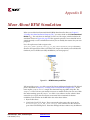
Appendix C: Glossary
6
www.xilinx.com
EDK Concepts, Tools, and Techniques
P/N XTP013 (v. 9.1i)
R
Preface
About This Guide
This guide explains the basics of the EDK embedded design flow, tools architecture, and
concepts behind the EDK design process. It also provides an opportunity for you try out
the EDK tools by taking them for a “test drive,” following a sample project. Specifications
for the sample project are provided.
Guide contents include:
Chapter 1, “Introduction”
Chapter 2, “Creating a New Project”
Chapter 3, “Xilinx Platform Studio (XPS)”
Chapter 4, “The Embedded Hardware Platform”
Chapter 5, “Creating Your Own Intellectual Property (IP)”
Chapter 6, “The Software Platform and SDK”
Chapter 7, “Introduction to Simulation in XPS”
Chapter 8, “Implementing and Downloading Your Design”
Chapter 9, “Debugging the Design”
Appendix A, “Embedded Submodule Design with ISE”
Appendix B, “More About BFM Simulation”
Additional Resources
To find additional EDK documentation, see the Xilinx® Website at:
http://www.xilinx.com/ise/embedded/edk_docs.htm.
To search the Answer Database for silicon, software, and IP questions and answers, or to
create a technical support WebCase, see the Xilinx Website at:
http://www.xilinx.com/support.
EDK Concepts, Tools, and Techniques
P/N XTP013 (v. 9.1i)
www.xilinx.com
7
R
Preface: About This Guide
Conventions
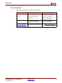
This document uses the following conventions. An example illustrates each convention.
Typographical
This document uses the following typographical conventions:
Convention
Meaning or Use
Courier font
Messages, prompts, and
program files that the system
displays
speed grade: - 100
Courier bold
Literal commands that you
enter in a syntactical statement
ngdbuild design_name
Commands that you select
from a menu
File > Open
Keyboard shortcuts
Ctrl+C
Variables in a syntax
statement for which you must
supply values
ngdbuild design_name
References to other manuals
See the Development System
Reference Guide for more
information.
Emphasis in text
If a wire is drawn so that it
overlaps the pin of a symbol,
the two nets are not connected.
An optional entry or
parameter. However, in bus
specifications, such as
bus[7:0], they are required.
ngdbuild [option_name]
design_name
A list of items from which you
must choose one or more
lowpwr ={on|off}
Separates items in a list of
choices
lowpwr ={on|off}
Vertical ellipsis
.
.
.
Repetitive material that has
been omitted
IOB #1: Name = QOUT’
IOB #2: Name = CLKIN’
.
.
.
Horizontal ellipsis . . .
Repetitive material that has
been omitted
allow block
loc1 loc2 ... locn;
Helvetica bold
Italic font
Square brackets
Braces
[ ]
{ }
Vertical bar
8
Example
|
www.xilinx.com
block_name
EDK Concepts, Tools, and Techniques
P/N XTP013 (v. 9.1i)
R
Conventions
Online Document
The following conventions are used in this document:
Convention
Meaning or Use
Example
See the section “Additional
Resources” for details.
Blue text
Cross-reference link to a
location in the current
document
Red text
Cross-reference link to a
location in another document
See Figure 2-5 in the
Virtex™-II Handbook.
Blue, underlined text
Hyperlink to a Website (URL)
Go to http://www.xilinx.com
for the latest speed files.
EDK Concepts, Tools, and Techniques
P/N XTP013 (v. 9.1i)
www.xilinx.com
Refer to “Title Formats” in
Chapter 1 for details.
9
R
10
Preface: About This Guide
www.xilinx.com
EDK Concepts, Tools, and Techniques
P/N XTP013 (v. 9.1i)
R
Chapter 1
Introduction
Welcome
The Xilinx® Embedded Development Kit (EDK) is a suite of tools and IP that enables you
to design a complete embedded processor system for implementation in a Xilinx Field
Programmable Gate Array (FPGA) device.
This guide describes the design flow for developing a custom embedded processing
system using EDK. Some background information is provided, but the main focus is on the
features of EDK and their use during the design process.
Read this document if you:
•
Need an introduction to EDK and its utilities
•
Have not designed an embedded processor system for a while
•
Are in the process of installing the Xilinx EDK tools
•
Would like a quick reference while designing a processor system
Note: This guide is written based on Windows operating system behavior. Linux and Solaris
behavior or graphical user interface (GUI) display may vary slightly.
Take a Test Drive!
Because the best way to learn a software tool is to use it, this document provides
opportunities for you to work with (“Test Drive”) the tools under discussion.
Specifications for a sample project are given in the Test Drive sections, and the reasons for
their use are explained. Information about what happens when you run automated
functions is also described. Test Drives are indicated by the car icon, as indicated in the
heading above.
Additional Documentation
More detailed documentation on EDK is available on the Xilinx web page:
http://www.xilinx.com/ise/embedded/edk_docs.html
Documentation on the Xilinx Integrated Software Environment (ISE™) is available on the
Xilinx web page: http://www.xilinx.com/support/software_manuals.htm.
EDK Concepts, Tools, and Techniques
P/N XTP013 (v. 9.1i)
www.xilinx.com
11
R
Chapter 1: Introduction
How EDK Simplifies Embedded Processor Design
Embedded systems are complex. Getting the hardware and software portions of an
embedded design to work are projects in themselves. Merging the two design components
so they function as one system creates additional challenges. Add an FPGA design project
to the mix, and the situation has the potential to become very confusing indeed.
To simplify the design process, Xilinx offers several sets of tools. It is a good idea to get to
know the basic tool names, project file names, and acronyms for these. To make this easier
for you, see the “Glossary” of EDK-specific terms provided at the back of this document.
The Integrated Software Environment (ISE)
ISE is the foundation for Xilinx FPGA logic design. Because FPGA design can be an
involved process, Xilinx has provided software development tools that allow the designer
to circumvent some of this complexity. Various utilities such as constraints entry, timing
analysis, logic placement and routing, and device programming have all been integrated
into ISE. For information on how to use the ISE tools for FPGA design refer to the Xilinx
web page: http://www.xilinx.com/support/software_manuals.htm.
The Embedded Development Kit (EDK)
EDK is a suite of tools and IP that enables you to design a complete embedded processor
system for implementation in a Xilinx FPGA device. To run EDK, ISE must be installed as
well. Think of it as an umbrella covering all things related to embedded processor systems
and their design.
Xilinx Platform Studio (XPS)
XPS is the development environment or GUI used for designing the hardware portion of
your embedded processor system.
Software Development Kit (SDK)
Platform Studio SDK is an integrated development environment, complimentary to XPS,
that is used for C/C++ embedded software application creation and verification. SDK is
built on the Eclipse™ open-source framework. Because many other software development
tools are being built on the Eclipse infrastructure, this software development tool might
already be familiar to you or members of your design team.
Other EDK Components
EDK includes other elements such as:
•
Hardware IP for the Xilinx embedded processors
•
Drivers and libraries for embedded software development
•
GNU Compiler and debugger for C/C++ software development targeting the
MicroBlaze™ and PowerPC™ processors
•
Documentation
•
Sample projects
The utilities provided with EDK are designed to assist in all phases of the embedded
design process.
12
www.xilinx.com
EDK Concepts, Tools, and Techniques
P/N XTP013 (v. 9.1i)
R
How Do the Tools Expedite the Design Process?
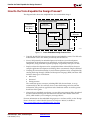
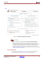
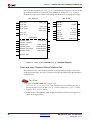
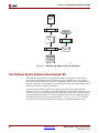
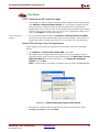
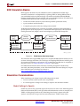
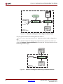
How Do the Tools Expedite the Design Process?
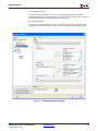
The diagram below shows the simplified flow for an embedded design.I
Xilinx Platform Studio (XPS)
Software
Development
Software
Development
Kit (SDK)
Hardware
Development
External
Simulator
Verification
Device
Configuration
ISE
Figure 1-1:
X10506
Basic Embedded Design Process Flow
•
Typically, the ISE FPGA development software runs behind the scenes. The XPS tools
make function calls to the utilities provided by the ISE software.
•
You use XPS primarily for embedded processor hardware system development.
Specification of the microprocessor, peripherals, and the interconnection of these
components, along with their respective property assignments, takes place in XPS.
•
Simple software development can be accomplished from within XPS, but for more
complex application development and debug, Xilinx recommends using the SDK tool.
•
Verifying the correct functionality of your hardware platform can be accomplished by
running the design through a Hardware Description Language (HDL) simulator. XPS
facilitates three types of simulation:
♦
Behavioral
♦
Structural
♦
Timing-accurate
The verification process structure, including HDL files for simulation, is set up
automatically by XPS. You will only have to enter clock timing and reset stimulus
information, along with any application code. Simulation will be covered in greater
detail later in this guide.
•
After you have completed your design, you can click a menu item in XPS to download
the FPGA bitstream along with the software Executable and Linkable Format file
(ELF), which enables you to configure your target device.
For more information on the embedded design process as it relates to XPS, see the “Design
Process Overview” in the Embedded Systems Tools Reference Manual, available at:
http://www.xilinx.com/ise/embedded/edk_docs.htm.
EDK Concepts, Tools, and Techniques
P/N XTP013 (v. 9.1i)
www.xilinx.com
13
R
Chapter 1: Introduction
Before Starting
Before discussing the tools in depth, it would be a good idea to make sure they are installed
properly and that the environments you have set up match those you will need to follow
the “Test Drive” sections in this document.
Installation Requirements: What You Need to Run EDK Tools
ISE
Several utilities in EDK use functionality delivered with tools contained in ISE. So, to use
the EDK tools, you first need to have the ISE tools installed. Be sure you have also installed
the latest ISE service packs as well. For information go to http://www.xilinx.com. From
there, choose the download link in the upper right corner.
Bash Shell for Linux or Solaris
If you are running EDK on a Linux or Solaris platform, you need a bash shell. Also, be sure
to check out the supported platforms covered in the Xilinx document Getting Started with
the Embedded Development Kit (EDK), available at:
http://www.xilinx.com/ise/embedded/edk_docs.htm.
Software Registration ID
You’ll need a software registration ID to install EDK. You can get one online at:
http://www.xilinx.com/ise/embedded/register.htm.
EDK Installation
Xilinx distributes EDK as a single, media-installable DVD image. Insert the DVD into your
PC. The installer launches automatically. For more information online:
http://www.xilinx.com/ise/embedded/edk_docs.htm.
Note: ISE and EDK major versions must be the same. For example, if you are installing EDK v 9.1i,
you must also install ISE v 9.1i.
Installation Requirements for Simulation
To perform simulation using the EDK tools, you must have the following steps completed:
1.
A SmartModel-capable simulator (ModelSim PE/SE or NCSim) is required for the
simulation steps. MXE will not work for SmartModels.
2.
Install the CoreConnect™ Toolkit. CoreConnect is a free utility provided by IBM®. You
can download CoreConnect from the Xilinx website at:
http://www.xilinx.com/xlnx/xebiz/designResources/ip_product_details.jsp?key=d
r_pcentral_coreconnect.
After you make the appropriate selections on the web page to order and register, you
will have access to the download.
3.
14
If you haven’t already done so, compile the simulation libraries following the
procedure outlined in the EDK help system available in XPS or on the Xilinx web page
under “Xilinx Platform Studio Help Topics” at
http://www.xilinx.com/ise/embedded/edk_docs.htm.
a.
If you are opening the help from XPS, select Help > Help Topics.
b.
Navigate to Procedures for Embedded Processor Design > Simulation >
Compiling Simulation Libraries in XPS > Compiling Simulation Libraries in
XPS.
www.xilinx.com
EDK Concepts, Tools, and Techniques
P/N XTP013 (v. 9.1i)
R
How Do the Tools Expedite the Design Process?
4.
To be sure your simulator is set up to handle SmartModels, refer to the help system.
From the contents list, select Procedures for Embedded Processor Design >
Simulation > Setting Up SmartModels.
For additional details on the installation process see “Getting Started with the Embedded
Development Kit (EDK)” at: http://www.xilinx.com/ise/embedded/edk_docs.htm.
EDK Concepts, Tools, and Techniques
P/N XTP013 (v. 9.1i)
www.xilinx.com
15
R
16
Chapter 1: Introduction
www.xilinx.com
EDK Concepts, Tools, and Techniques
P/N XTP013 (v. 9.1i)
R
Chapter 2
Creating a New Project
Now that you’ve been introduced to EDK, let’s begin looking at how you use the tools to
develop an embedded system.
The Base System Builder (BSB)
BSB is a wizard that quickly and efficiently establishes a working design, which you can
then customize.
At the end of this section, you will have the opportunity to begin your test drive, using BSB
to create a project.
Why Should I Use BSB?
Xilinx® recommends using the BSB Wizard to create, at minimum, a foundation for any
new embedded design project. BSB may be all you need to create your design, but if more
customization is required, BSB can save you a lot of time because it automates basic
hardware and software platform configuration tasks common to most processor designs.
After running the wizard, you have a working project that contains all the basic elements
needed to build a more customized or complex system, should that be necessary.
What You Can Do in the BSB Wizard
Using the BSB Wizard, you can create your project file, choose a board, select and configure
a processor and I/O interfaces, add internal peripherals, set up software, and generate a
system summary report.
BSB recognizes the system components and configurations as you build it and provides the
options appropriate to your selections.
Creating Your Top-level Project File (*.xmp File)
File creation includes the option to apply settings from another project you have created
with the BSB.
The Xilinx
Microprocessor
Project (*.xmp) file
A Xilinx Microprocessor Project (XMP) file is the top-level file description of the embedded
system under development. All XPS project information is saved in the XMP file, including
the location of the Microprocessor Hardware Specification (MHS) and Microprocessor
Software Specification (MSS) files. The MHS and MSS files are described in detail later.
The XMP file also contains information about C source and header files that XPS is to
compile, as well as any executable files that the Software Development Kit (SDK) compiles.
The project also includes the FPGA architecture family and the device type for which the
hardware tool flow must be run.
EDK Concepts, Tools, and Techniques
P/N XTP013 (v. 9.1i)
www.xilinx.com
17
R
Chapter 2: Creating a New Project
Selecting a Board Type
BSB allows you to select a board type from a list or to create a custom board.
Supported Boards
Base System Builder
(BSB)
If you are targeting one of the supported embedded processor development boards
available from Xilinx or from one of our partners, BSB lets you choose from the peripherals
available on that board, automatically match the FPGA pinout to the board, and create a
completed platform and test application ready to download and run on the board. Each
option has functional default values that are pre-selected in XPS. This base-level project
can be further enhanced in XPS, or it can be implemented using the Xilinx implementation
utilities provided by ISE.
Custom Boards
If you are developing a design for a custom board, BSB lets you select and interconnect one
of the available processor cores (MicroBlaze™ or PowerPC™, depending on your selected
target FPGA device) with a variety of compatible and commonly used peripheral cores
from the IP library. This gives you a hardware system to use as a starting point. You can
add more processors and peripherals if needed. The utilities provided in XPS assist with
this, including the creation of custom peripherals.
Selecting and Configuring a Processor
You can choose a MicroBlaze or PowerPC processor and select:
•
•
•
•
•
Architecture type
Device type
Package
Speed grade
Reference clock frequency
•
•
•
•
•
Processor-bus clock frequency
Reset polarity
Processor configuration for debug
Cache setup
Floating Point Unit (FPU) setting
Selecting and Configuring Multiple I/O Interfaces
BSB understands the external memory and I/O devices available on your predefined
board and allows you to select the following, as appropriate to a given device:
•
Which devices to use
•
Baudrate (bps)
•
Peripheral type
•
Number of data bits
•
Parity
•
Whether or not to use interrupts
For your convenience, data sheets for external memory and I/O devices can be opened
from within the wizard.
Adding Internal Peripherals
BSB allows you to add additional peripherals of your choice. There is a caveat: the
peripherals are supported by the selected board and FPGA device architecture. For a
custom board, certain peripherals are available for general selection and automatic system
connection.
18
www.xilinx.com
EDK Concepts, Tools, and Techniques
P/N XTP013 (v. 9.1i)
R
The Base System Builder (BSB)
Setting Up Software
Standard input and output devices can be specified in BSB, and you can select sample C
applications that you would like XPS to generate. Each application includes a linker script.
The sample applications from which you can select include a memory test, peripheral test,
or both.
Viewing a System Summary Page
After you have made your selections in the wizard, BSB displays a system summary page.
You can choose to generate the project, or you can go back to any previous wizard dialog
box and revise the settings.
Test Drive!
Run the BSB Wizard to begin your Test Drive. The wizard opens when you launch XPS. Or,
if XPS is already open, select File > New Project and choose BSB from the resulting dialog
box.
Build a project that has the following characteristics:
Wizard Screens
System Property
Setting to Use for Your Test Drive
Create New XPS Project
Using BSB Wizard
Project name
Name your project system.xmp. Be sure to create a
new directory for the project.
Welcome
Project type
Select the option to create a new project.
Select Board
Board vendor and name.
Choose Xilinx as your board vendor and select the
Virtex 4 ML403 Evaluation Platform.
The ML403 board contains a Virtex™-4 FX device,
which means BSB allows you to select either a
MicroBlaze or PowerPC soft processor core.
Select Processor
Processor.
Select PowerPC.
Configure PowerPC
• Clock frequencies.
• Use defaults.
• Processor Debug
Interface (Debug I/F)
Configuration.
• Use default: FPGA JTAG.
This means that the JTAG pins will also be used for
processor debug.
• On-chip memory.
• Use 16 KB of data and instruction BRAM.
Xilinx-provided IP
selections.
Select, at a minimum, RS-232_Uart,
Push_Buttons_Position, SRAM_256Kx32.
Configure IO Interfaces
(four screens)
Add any additional IP, if you wish to do so.
Any IP that must be purchased is displayed with an
accompanying lock symbol. You can evaluate the IP for
a period of time, but it must be purchased to continue
working in your design.
Add Internal
Peripherals
Default is
plb_bram_if_cntlr_1
with 16 KB memory size.
EDK Concepts, Tools, and Techniques
P/N XTP013 (v. 9.1i)
Use default.
www.xilinx.com
19
R
Chapter 2: Creating a New Project
Wizard Screens
System Property
Software Setup
• Software setup
Setting to Use for Your Test Drive
• Select your STDIN/OUT device(s).
In the BSB software setup
dialog boxes you specify
how you would like to
use your system. BSB can
also set up any software
tests you would like to
create.
Be sure the RS232_Uart peripheral is one of these.
• Boot memory
• plb_bram_if_cntlr_1
• Memory and peripheral
tests
• Use default application tests.
The software tests send or
receive information to
selected peripherals. The
microprocessor interprets
the status of the
peripherals and reports it
via the STDIN/STDOUT
peripheral.
Configure Memory Test
Application
Configure Peripheral
Test Application
System Created
Instruction, Data, and
Stack/Heap memory
locations.
For the purposes of this project, place these in
plb_bram_if_cntlr_1.
System summary page.
After you have selected and configured all your system
components, BSB displays an overview of the system,
which allows you to verify your selections. At this
point, you have an opportunity to go back to any
previous wizard dialog box and make revisions.
This specifies that the program code operates out of the
block RAM contained in the FPGA (plb_bram) using
the BRAM controller (_if_cntlr_1).
When the system summary looks correct, click
Generate.
Finish
20
During design generation,
the directory structure of
your system is created. The
HDL and other files are
populated with the choices
you made earlier, and
connections between the
processor, busses, and
peripherals are handled,
along with any additional
logic being instantiated.
When you click Finish, XPS is populated with the
system you just created.
www.xilinx.com
EDK Concepts, Tools, and Techniques
P/N XTP013 (v. 9.1i)
R
What’s Next?
What’s Next?
In the next chapter, you will learn how you can view and modify the characteristics of your
new project in XPS.
Creating Your BSB Variant
Creating a custom board library involves creating a Xilinx Board Description file (*.xbd)
and placing it in the $XILINX_EDK/board location. For more information on this topic
see the "Xilinx Board Description (XBD)" chapter of the Platform Specification Format
Reference Manual, available at http://www.xilinx.com/ise/embedded/edk_docs.htm.
EDK Concepts, Tools, and Techniques
P/N XTP013 (v. 9.1i)
www.xilinx.com
21
R
22
Chapter 2: Creating a New Project
www.xilinx.com
EDK Concepts, Tools, and Techniques
P/N XTP013 (v. 9.1i)
R
Chapter 3
Xilinx Platform Studio (XPS)
Now that you have created a baseline project with BSB, it’s time to take a look at the
options available to you in Xilinx Platform Studio (XPS). Using XPS, you will be able to
build on the project you created with BSB. This chapter takes you on a tour of XPS.
Subsequent chapters in the document discuss how to use XPS to modify your design.
Note: Taking the tour of XPS provided in this chapter is recommended. It will enable you to more
easily follow the rest of this book and other documentation on XPS.
What is XPS?
XPS includes a graphical user interface (GUI), along with a set of tools that aid in project
design. This chapter describes the XPS GUI and some of the most commonly implemented
tools.
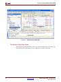
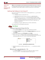
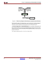
The XPS GUI
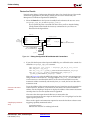
From the XPS GUI, you can design a complete embedded processor system for
implementation within a Xilinx FPGA device. The XPS main window is shown in the
figure below.
Note that the XPS main window is divided into three areas:
•
The Project Information Panel
•
The System Assembly Panel
•
The Console Panel
Optional test drives are provided in this chapter so you can explore the information and
tools available in each of the XPS main window areas.
EDK Concepts, Tools, and Techniques
P/N XTP013 (v. 9.1i)
www.xilinx.com
23
R
Chapter 3: Xilinx Platform Studio (XPS)
Connectivity Panel
System Assembly
Panel
Project Information
Panel
Console Panel
Figure 3-1:
Xilinx Platform Studio GUI
The Project Information Panel
The Project Information panel offers control over and information about your project. The
Project Information panel provides Project, Applications, and IP Catalog tabs.
24
www.xilinx.com
EDK Concepts, Tools, and Techniques
P/N XTP013 (v. 9.1i)
R
The XPS GUI
The Project Tab
The Project Tab lists references to projectrelated files. Information is grouped in the
following general categories:
• Project Files
All project-specific files such as the
Microprocessor Hardware Specification
(MHS) files, Microprocessor Software
Specification (MSS) files, User
Constraints File (UCF) files, iMPACT
Command files, Implementation
Option files, and Bitgen Option files
• Project Options
All project-specific options, such as
Device, Netlist, Implementation,
Hardware Description Language
(HDL), and Sim Model options
• Reference Files
Figure 3-2:
All log and output files produced by the
XPS implementation processes
Project Information Area:
Project Tab
The Applications Tab
The Applications tab lists all software
application option settings, header files,
and source files associated with each
application project. With this tab
selected, you can:
• Create and add a software
application project, build the project,
and load it to the block RAM
• Set compiler options
• Add source and header files to the
project
Figure 3-3:
EDK Concepts, Tools, and Techniques
P/N XTP013 (v. 9.1i)
www.xilinx.com
Project Information Area:
Applications Tab
25
R
Chapter 3: Xilinx Platform Studio (XPS)
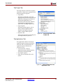
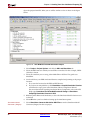
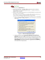
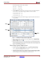
The IP Catalog Tab
The IP Catalog tab lists all the EDK IP
cores and any custom IP cores you
created.
If a project is open, only the IP cores
compatible with the target Xilinx
device architecture are displayed. The
catalog lists information about the IP
cores, including release version, status
(active, early access or deprecated),
lock (not licensed, locked, or
unlocked), processor support, and a
short description.
Additional details about the IP core,
including the version change history,
data sheet, and Microprocessor
Peripheral Description (MPD) file, are
available in the right-click menu.
By default, the IP cores are grouped
hierarchically by function.
Figure 3-4:
Project Information Area:
IP Catalog Tab
Test Drive!
•
Click the Project tab. Notice that right-clicking a project file lets you open it in XPS
and that a right-click on an item under Project Options allows you to open the Project
Options dialog box.
•
Click the Applications tab.
•
26
♦
Collapse the Project: TestApp_Memory (using the +/- box).
♦
Expand the four sub-headers below Project: TestApp_Peripheral.
-
Under Processor: ppc405_0 note the xparameters.h file, which will be
referenced later in this guide. The xparameters.h file contains the system
address map and is an integral part of the Board Support Package (BSP). If
you have been following the previous test drive steps, the BSP has not been
generated yet, so this file is unavailable.
-
Under Compiler Options and Sources, note that both a linker script and test
application sources were automatically created by the BSB Wizard as part of
creating the selected test applications.
Click the IP Catalog tab.
♦
Find the Communication Low-Speed IP category and expand it.
♦
Locate the OPB_UART (Lite) peripheral and right-click to review the available
options.
♦
Note the option to select a flat or hierarchical view. Click the directories icon
circled in Figure 3-4, above, to switch between the two views.
www.xilinx.com
EDK Concepts, Tools, and Techniques
P/N XTP013 (v. 9.1i)
R
The XPS GUI
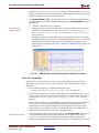
The System Assembly Panel
The System Assembly Panel is where you view and configure system block elements.
If the System Assembly Panel is not already maximized in the main window, click the
System Assembly tab at the bottom of the pane to open it.
Bus Interface, Ports, and Address Filters
XPS provides Bus Interface, Ports, and Addresses radio buttons in the System
Assembly Panel (shown in the figure below), which organize information about your
design and allow you to edit your hardware platform more easily.
Figure 3-5:
System Assembly Panel Views
The Connectivity Panel
With the Bus Interface filter selected, you’ll see the Connectivity Panel, highlighted by the
dashed line in Figure 3-5. The Connectivity Panel is a graphical representation of the
hardware platform interconnects.
•
A vertical line represents a bus, and a horizontal line represents a bus interface to an
IP core.
•
If a compatible connection can be made, a connector is displayed at the intersection
between the bus and IP core bus interface.
•
The lines and connectors are color-coded to show the compatibility.
•
Differently shaped connection symbols indicate mastership of the IP core bus
interface.
•
A hollow connector represents a connection that you can make, and a filled connector
represents a connection made. To create or disable a connection, click the connector
symbol.
EDK Concepts, Tools, and Techniques
P/N XTP013 (v. 9.1i)
www.xilinx.com
27
R
Chapter 3: Xilinx Platform Studio (XPS)
Information Viewing and Sorting
To allow you to sort information and revise your design more easily, the System Assembly
Panel provides two view options: hierarchical view and flat view.
Hierarchical and Flat Views
Hierarchical view is the default in the System Assembly Panel. In the hierarchical view, the
information about your design is based on the IP core instances in your hardware platform
and organized in an expandable or collapsible tree structure.
When you click the directory structure icon (circled in Figure 3-5), the ports are displayed
either hierarchically or in a flattened, or flat, view.
The flat view allows you to sort information in the System Assembly Panel
alphanumerically by any column.
Expanded or Collapsed Nodes
The +/- icon, also circled, expands or collapses all nets or buses associated with an IP. This
allows quick association of a net with the IP elements.
Test Drive!
In the System Assembly Panel:
•
Click the Ports radio button located at the top of the System Assembly Panel.
♦
Expand the External Ports category to view the signals that are present outside
the FPGA device. Note the names of the signals in the Net column and find the
signals related to the RS232_Uart. (You may need to drag the right side of the Net
column header to see its entire contents.) These are referenced in the next step.
Collapse this category when finished.
♦
Find the RS232_Uart peripheral and expand it. Note the Net names and how
they correspond to the names that were present as external signals. The RX and
TX net from the UART are name-associated with the external ports.
♦
Double-click the RS232_Uart peripheral icon to launch the
RS232_Uart: opb_uartlite_v1_00_b parameters dialog box. You can use the
parameters dialog box for any peripheral to adjust various settings available for
the IP. Take a moment and observe what happens when you hover the cursor over
a parameter name. Note the three top buttons and the tabs available for this core.
Close this box when finished.
♦
Click the directories icon (circled in Figure 3-5), and switch between the
hierarchical and flat views.
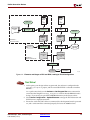
The Platform Studio Tab
In the same space as the System Assembly Panel, there is a tab labeled Platform Studio.
The Platform Studio tab display, shown in the figure below, provides an embedded design
flow diagram, with links to related help topics. If at any point you are not sure what to do
next, or need more information on how to perform a process, you can refer to this diagram
for a quick update.
28
www.xilinx.com
EDK Concepts, Tools, and Techniques
P/N XTP013 (v. 9.1i)
R
The XPS GUI
Figure 3-6:
Platform Studio Startup Flow Diagram
Test Drive!
Note: If you can’t see the Platform Studio tab, click Help > View Startup Flow Diagram.
•
With the Platform Studio tab selected, try clicking the Software Development,
Hardware Development, and FPGA Device Configuration headings. You may find it
interesting to read the help topics overviews for these parts of the design flow.
•
Try clicking the Hardware Development topic “Begin by using the Base System
Builder.” This presents material with which you might now be familiar, after reading
Chapter 2, “Creating a New Project.”
The Console Panel
The Console panel, shown in Figure 3-1, page 24, provides feedback from the tools
invoked during runtime. Notice the three tabs: Output, Warning, and Error.
EDK Concepts, Tools, and Techniques
P/N XTP013 (v. 9.1i)
www.xilinx.com
29
R
Chapter 3: Xilinx Platform Studio (XPS)
XPS Tools
In addition to the GUI, XPS includes all the underlying tools needed to develop the
hardware and software components of an embedded processor system.
These include:
•
Base System Builder (BSB) Wizard, for creating new projects. The BSB dialog box that
appears on XPS start-up is also available from the toolbar. Click File > New Project.
•
Hardware Platform Generation tool (Platgen), for generating the embedded processor
system. To start Platgen, click Hardware > Generate Netlist.
•
Simulation Model Generation tool (Simgen) generates simulation models of your
embedded hardware system based either on your original embedded hardware
design (behavioral) or finished FPGA implementation (timing-accurate). Click
Simulation > Generate Simulation HDL Files to start Simgen.
•
Create and Import Peripheral Wizard helps you create your own peripherals and
import them into EDK-compliant repositories or XPS projects. To start the wizard,
click Hardware > Create or Import Peripheral.
•
Library Generation tool (Libgen) configures libraries, device drivers, file systems, and
interrupt handlers for the embedded processor system, creating a software platform.
Click Software > Generate Libraries and BSPs to start Libgen.
•
Xilinx Platform Studio Software Development Kit (SDK) is a complementary interface
to XPS and provides a development environment for software application projects. To
open SDK, click Software > Launch Platform Studio SDK. For your convenience,
SDK has its own user interface, which expedites software design tasks.
Test Drive!
Take a look at the options available under the Hardware, Software, and Simulation menu
items.
XPS Directory Structure
The BSB has automated the project directory structure setup and started what can be
considered a simple but complete project. The time savings that BSB provides during
platform configuration can be negated, however, if you don’t understand what the tools
are doing behind the scenes. Let’s take a look at the directory structure that was created
and see how it could be useful as project development progresses.
Directories
BSB creates four primary directories automatically. These are shown in Figure 3-7.
30
_ _xps
Contains intermediate files generated by XPS and other tools for
internal project management. You will not use this directory.
data
Contains the user constraints file (UCF). For more information on this
file and how to use it, see the ISE UCF help topics at:
http://www.xilinx.com/support/software_manuals.htm.
www.xilinx.com
EDK Concepts, Tools, and Techniques
P/N XTP013 (v. 9.1i)
R
What’s Next?
etc
Contains files that capture the options used to run various tools. This
directory is empty because no actions outside of BSB have been
performed.
pcores
Used for including custom hardware peripherals.
There are two directories that contain the BSB-generated test application C-source code,
header files, and linker scripts, which were explored in an earlier Test Drive.
Underneath the main project directory you will also find a few files. Those of interest are
shown in the figure below and are described as follows.
system.xmp
This is the top-level project design file. XPS reads this file and
graphically displays its contents in the XPS user interface.
system.mhs
The system microprocessor hardware specification, or MHS file,
captures textually the system elements, their parameters, and
connectivity. The MHS file is the hardware foundation for your
project.
system.mss
The system microprocessor software specification, or MSS file,
captures the software portion of the design, describing textually the
system elements and various software parameters associated with the
peripheral. The MSS file is the software foundation for your project.
Figure 3-7:
Directories and Files Created When You Run the BSB Wizard
Test Drive!
Using a file explorer utility, navigate to the top-level directory for your project. Open the
various subdirectories and become familiar with the basic file set.
What’s Next?
Now that you know your way around XPS, you’re ready to begin working with the project
you started in Chapter 2, “Creating a New Project.” We will begin with the hardware
platform.
EDK Concepts, Tools, and Techniques
P/N XTP013 (v. 9.1i)
www.xilinx.com
31
R
32
Chapter 3: Xilinx Platform Studio (XPS)
www.xilinx.com
EDK Concepts, Tools, and Techniques
P/N XTP013 (v. 9.1i)
R
Chapter 4
The Embedded Hardware Platform
What’s in a Hardware Platform?
The embedded hardware platform includes one or more processors, along with a variety of
peripherals and memory blocks. These blocks of IP use an interconnect network to
communicate. Additional ports connect to the “outside world.” The behavior of each
processor or peripheral core can be customized. Various optional features are controlled
through implementation parameters, which specify what is ultimately implemented in the
FPGA. The implementation parameters also define the addresses for your system.
Hardware Platform Development in Xilinx Platform Studio
Microprocessor
Hardware
Specification (MHS)
XPS provides an interactive development environment that allows you to specify all
aspects of your hardware platform. XPS maintains your hardware platform description in
a high-level form, known as the Microprocessor Hardware Specification (MHS) file. The
MHS, an editable text file, is the principal source file representing the hardware component
of your embedded system. XPS synthesizes the MHS source file into Hardware
Description Language (HDL) netlists ready for FPGA place and route.
The MHS File
The MHS file is integral to your design process. It contains all peripherals along with their
parameters. The MHS file defines the configuration of the embedded processor system and
includes information on the bus architecture, peripherals, processor, connectivity, and
address space. For more detailed information on the MHS file, refer to the
“Microprocessor Hardware Specification (MHS)” chapter of the Platform Specification
Format Reference Manual, available at
http://www.xilinx.com/ise/embedded/edk_docs.htm. Because of its importance, let’s
take a quick tour of the MHS file that was created when you ran the BSB Wizard.
EDK Concepts, Tools, and Techniques
P/N XTP013 (v. 9.1i)
www.xilinx.com
33
R
Chapter 4: The Embedded Hardware Platform
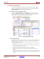
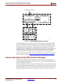
Test Drive!
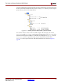
1.
Select the Project tab in the Project Information Area. Look under the Project Files
heading to find MHS File: system.mhs, as shown in the figure below. Double-click
the file name to open it.
Figure 4-1:
MHS File
2.
Search for opb_uartlite in the system.mhs file. Notice how the peripherals, their
ports, and their parameters are configured in the MHS file.
3.
Take some time to review other IP cores in your design.
4.
When you are finished close the system.mhs file.
Viewing the Hardware Platform from the System Assembly Panel
The System Assembly Panel area in XPS displays all hardware platform IP instances using
an expandable tree and table format. The first thing to notice is comments, which are
preceded by a pound sign (#). Next you will see global ports. These are called “global”
because they reside outside of a begin-end block.
XPS provides extensive display customization, sorting, and data filtering capability so you
can easily review your embedded design. The IP elements, their ports, properties, and
parameters, which are configurable in the System Assembly Panel, are written directly to
the MHS file. Editing a port name or setting a parameter takes effect when you press Enter
or click OK, respectively. XPS automatically writes the system modification to the
hardware database, which is contained in the MHS file. The recommended method for
editing the MHS file is to use the System Assembly Panel views.
Note: Adding, deleting, and customizing IP are discussed in Chapter 5, “Creating Your Own
Intellectual Property (IP).”
Generating Your Hardware Platform
To generate the hardware platform, you first tell XPS to generate a netlist and then issue
the command to generate the bitstream. This operation will be part of a future Test Drive
exercise. In the meantime, you probably want to know what happens when the netlist and
bitstream are created, so a quick synopsis is provided below:
Netlist Generation
When you tell XPS to generate the netlist, it invokes the platform building tool, Platgen,
which does the following:
34
♦
Reads the design platform configuration MHS file.
♦
Generates an HDL representation of the MHS file written to system.[vhd|v]
along with a system_stub.[vhd|v]. The system file is your MHS description
www.xilinx.com
EDK Concepts, Tools, and Techniques
P/N XTP013 (v. 9.1i)
R
What’s Next?
written in HDL format. This is for designs that are "processor-centric" and
developed solely in XPS. The file system_stub is a top level HDL template file
instantiation of the embedded system created as a starting point for "FPGAcentric" designs. FPGA-centric designs are those in which the embedded system is
a sub-module in a larger design.
♦
Synthesizes the design using Xilinx Synthesis Technology (XST).
♦
Produces a netlist file.
More information about PlatGen is available in the “Platform Generator (PlatGen)”
chapter in the Embedded System Tools Reference Manual, available at
http://www.xilinx.com/ise/embedded/edk_docs.htm.
Bitstream Generation
When you command XPS to generate the bitstream, Platgen verifies the presence of an
updated netlist. On successful completion of the Platgen process, the ISE
implementation tools run from batch mode. The ISE implementation tools read the
netlist created, and, in conjunction with a user constraints file (UCF), they produce a
BIT file containing your hardware design. Software patterns, if any, are not included. If
you used the BSB Wizard to create your initial hardware platform, it will have
generated a UCF in the XPS project data folder.
For more information on the UCF and its implementation, look for the XPS Help topic
Procedures for Embedded Processor Design > Adding Hardware Design
Elements > Implementing the Hardware Platform.
What’s Next?
Now you can start to customize your design. In the next chapter, you’ll add your own IP to
the Test Drive project.
EDK Concepts, Tools, and Techniques
P/N XTP013 (v. 9.1i)
www.xilinx.com
35
R
36
Chapter 4: The Embedded Hardware Platform
www.xilinx.com
EDK Concepts, Tools, and Techniques
P/N XTP013 (v. 9.1i)
R
Chapter 5
Creating Your Own Intellectual
Property (IP)
So far, it has been fairly easy to develop an embedded system using XPS. Everything you
have done up to this point has amounted to a series of mouse clicks because XPS has
automated the process for you. Invariably, however, you will want to add some degree of
customization to achieve your design goals. But this doesn’t mean the process has to
become hopelessly complex and slow; even when customizing a system, XPS gives you the
opportunity to automate many steps that would otherwise be error-prone and timeconsuming. That said, adding some custom logic (IP) to your Test Drive system would be
a good next step. Let’s get into some real design!
IP Creation Overview
If you think back to the XPS overview (see in particular Figure 3-1, page 24 and Figure 3-5,
page 27), the bus interface filter in the System Assembly Panel shows connections among
busses, processor, and IP. Any piece of IP you create must be compliant with the system
that is in place. To ensure compliance, the following must occur:
1.
The interface required by your IP must be determined.
The bus to which your custom peripheral will attach must be identified. For example:
Processor Local Bus
(PLB)
On-chip Peripheral
Bus (OPB)
a.
Processor Local Bus (PLB). The PLB provides a high-speed interface between the
processor and high-performance peripherals.
b.
On-chip Peripheral Bus (OPB). The OPB allows processor access to low-speed,
low-performance system resources.
For more information on these two primary processor busses, along with other
interconnects available, refer to the PowerPC 405 Processor Block Reference Guide
available at http://www.xilinx.com/ise/embedded/edk_docs.htm.
2.
Functionality must be implemented and verified.
Your custom functionality must be implemented and verified, with awareness that
common functionality available from the EDK peripherals library can be reused. Your
stand-alone core must be verified. Isolating the core ensures easier debug in the future.
3.
The IP must be imported to EDK.
Your peripheral must be copied to an EDK-appropriate directory, and the Platform
Specification Format (PSF) interface files (MPD and PAO) must be created, so other
EDK tools can recognize your peripheral.
4.
Your peripheral must be added to the processor system created in XPS.
EDK Concepts, Tools, and Techniques
P/N XTP013 (v. 9.1i)
www.xilinx.com
37
R
Chapter 5: Creating Your Own Intellectual Property (IP)
How to Do It: Use the CIP Wizard!
You are probably saying to yourself, “This sounds complicated. How do I use XPS to make
all this happen?” Fortunately, XPS offers another useful wizard, the Create and Import
Peripheral (CIP) Wizard. The CIP Wizard assists with steps two and three above by
walking you through the IP creation process. It sets up a number of templates for you to
populate with proprietary logic. In addition to creating HDL templates, the CIP Wizard
creates a peripheral core (pcore) verification project for Bus Functional Model (BFM)
verification. The templates and the BFM project creation are great for jump starting your IP
development as well as ensuring your IP will comply with the system you created or will
create.
The Create and Import Peripheral (CIP) Wizard
By asking a few simple questions, the CIP Wizard greatly simplifies your custom
peripheral creation process. Let’s walk through creating a blank template for a piece of
proprietary IP that you will design. For simplicity, most steps will accept default values,
but you will have a chance to see all the possible selections you can make.
What You Need to Know Before Running the CIP Wizard
CoreConnect-Compliant Peripherals
The wizard can create four types of CoreConnect™-compliant peripherals using
predefined IP interface (IPIF) libraries. These are:
•
OPB slave-only peripheral
•
OPB master-slave combo peripheral
•
PLB slave-only peripheral
•
PLB master-slave combo peripheral
To learn more about the CoreConnect interface, review the following documents
appropriate to the bus to which your IP will connect:
OPB Bus
$XILINX_EDK\doc\usenglish\opb_ipif_arch.pdf
$XILINX_EDK\doc\usenglish\opb_usage.pdf
PLB Bus
$XILINX_EDK\doc\usenglish\plb_usage.pdf
Data Sheets
An easy way to find data sheets for a given element (PLB or OPB Bus) in the IP catalog:
Right-click the IP element and select View PDF Datasheet.
38
www.xilinx.com
EDK Concepts, Tools, and Techniques
P/N XTP013 (v. 9.1i)
R
The Create and Import Peripheral (CIP) Wizard
Test Drive!
In the XPS toolbar, select Hardware > Create or Import Peripheral.
Create your new peripheral so that it has the characteristics described in the table below.
Wizard Screen
Wizard Requested Input
Value to Enter (when in doubt select default
value)
Peripheral Flow
Set the wizard to create a new
peripheral.
Select the Create templates for a new
peripheral radio button to begin creating your
new IP. Store the peripheral in your XPS project.
Both steps are default options.
Repository or Project
Specify the location to which
you want to save the
peripheral.
Select the To an XPS Project option and browse
the location of the current project. This may be
pre-selected.
Name and version
Peripheral name and version
number.
Give the new peripheral the name test_ip.
Use the default version 1_00_a
Bus Interface
Bus type.
Select OPB (default).
IPIF Services
IPIF services requested.
Select all basic services, as well as a FIFO under
the advanced services.
FIFO Services
FIFO services requested.
Use default values for FIFO and for Interrupt
services.
Interrupt Service
Configure interrupt
handling.
Use defaults.
User S/W Register
Software register
configuration.
Use defaults.
IP Interconnect (IPIC)
IP interconnect (IPIC)
signals.
Use defaults.
Note: Click a signal name to view additional
information about a signal you might wish to adjust.
Peripheral Simulation
Support
Bus functional model
simulation.
Note: If either of the two conditions below is not met,
skip this step.
Select an EDK-capable simulator (ModelSim
PE/SE or NCSim).
• You must have the BFM toolkit installed, or
you won’t be able to select the BFM checkbox.
• You must have ModelSim or NCSim installed.
Peripheral Implementation
Support
Peripheral implementation
support.
Use defaults.
Finish
Create Peripheral, Finish.
Review the details contained in the wizard
screen text box. Note the interrupt address range
given. Click Finish.
Note: For additional information about the Create and Import Peripheral Wizards, see the XPS help system topic set at
Procedures for Embedded Processor Design > Creating and Importing Peripherals. The Xilinx web provides IP interface
documentation at http://www.xilinx.com/ise/embedded/edk_ip.htm.
EDK Concepts, Tools, and Techniques
P/N XTP013 (v. 9.1i)
www.xilinx.com
39
R
Chapter 5: Creating Your Own Intellectual Property (IP)
What Just Happened?
The wizard worked! But you’re probably not sure what it really produced. Let’s stop for a
moment and examine some concepts and the resulting output.
Intellectual Property Interface (IPIF)
Intellectual Property
Interface (IPIF)
Library & IP
Interconnect (IPIC)
EDK uses what is called an Intellectual Property Interface (IPIF) library to implement
common functionality among various processor peripherals. In the Bus Interface and IPIF
Services Panels, the CIP Wizard asked you to define the target bus and what services the IP
would need. The purpose here was to determine the IPIF elements your IP would require.
The IPIF is a verified, optimized, and highly parameterizeable interface. It also gives you a
set of simplified bus protocols. This is called IP Interconnect (IPIC), which is much easier to
work with when compared to operating on the OPB or PLB bus protocol directly. Using the
IPIF module with parameterization that suits your needs greatly reduces your design and
test effort because you don’t have to re-invent the wheel. The figure below illustrates the
relationship between the bus, IPIF, IPIC, and your user logic.
Figure 5-1:
Using the IPIF Module in Your Custom Peripheral
Now, to draw the parallels between what the wizard created and the boxes in the figure
above:
The CIP Wizard created two template files that assist in IP connection. The top-level file is
given the name you entered: test_ip.vhd. The second file, user_logic.vhd, is where
your custom logic is to be connected.
40
www.xilinx.com
EDK Concepts, Tools, and Techniques
P/N XTP013 (v. 9.1i)
R
The Create and Import Peripheral (CIP) Wizard
A review of the directory structure and files that were created by the wizard reveals where
the above-mentioned and other key files reside. See the pcores directory in your example
project directory, shown in the figure below.
Figure 5-2:
Directory Structure Generated by the CIP Wizard
Our attention will now focus on the two VHDL template files created by the wizard,
test_ip.vhd and user_logic.vhd, shown in the figure above. The user_logic file
makes the connection to the OPB bus via the IPIF core configured in test_ip.vhd. The
user_logic.vhd file is equivalent to the “Custom Functionality” block and the
test_ip.vhd file is equivalent to the IPIF block; both blocks are shown in Figure 5-1,
page 40.
EDK Concepts, Tools, and Techniques
P/N XTP013 (v. 9.1i)
www.xilinx.com
41
R
Chapter 5: Creating Your Own Intellectual Property (IP)
In this Test Drive example, the user_logic.vhd block diagram appears as shown in the
figure below. The IPIF core connection to the OPB bus is made in test_ip.vhd and
shown in the figure below. What is still lacking from both files is your proprietary logic.
user_logic.vhd
Bus2IP_Data
test_ip.vhd
OPB_ABus
IP2Bus_Data
OPB_DBus
Bus2IP_BE
Bus2IP_RdCE
IP2Bus_Ack
Bus2IP_WrCE
IP2Bus_Retry
SI_DBus
OPB_BE
SI_errAck
IP2Bus_Error
Bus2IP_Clk
Bus2IP_Reset
OPB_Clk
SI_retry
OPB_Rst
SI_toutSup
OPB_RNW
SI_xferAck
OPB_select
FIFO Signals
OPB_seqAddr
RFIFO2IP_WrAck
IP2INTC_Irpt
IP2FIFO_Data
X10513
RFIFO2IP_AlmostFull
RFIFO2IP_Full
IP2Bus_ToutSup
WFIFO2IP_RdAck
IP2RFIFO_WrReq
WFIFO2IP_AlmostEmpty
IP2WFIFO_RdReq
WFIFO2IP_Empty
IP2Bus_IntrEvent
WFIFO2IP_Data
X10512
Figure 5-3:
user_logic.vhd and test_ip.vhd Block Diagrams
Create and Import Peripheral Wizard Template Files
This brief discussion of the interface provides the background you need to create some
usable proprietary logic. Let’s take a test drive to review the template files the Wizard has
created for you.
Test Drive!
42
1.
In XPS, select File > Open and navigate to the
pcores\test_ip_v1_00_a\hdl\vhdl directory. Here you will find two files as
listed in Figure 5-2, page 41: the test_ip.vhd file and the user_logic.vhd file.
2.
Open the user_logic.vhd file.
3.
Search for the value entity user_logic and find the occurrence that appears as
shown in the figure below.
www.xilinx.com
EDK Concepts, Tools, and Techniques
P/N XTP013 (v. 9.1i)
R
The Create and Import Peripheral (CIP) Wizard
Insert USER value
Figure 5-4:
user_logic.vhd Template File
Wherever user information is required in the two template files (<ip core name>.vhd
and user_logic.vhd), you will find comments indicating the type of information
required and where to place it.
Because the templates create CoreConnect-compliant structures, you will not add any
additional logic to your Test Drive project. However, it would be a good idea to view the
bare interface setup and operation for future understanding.
Intellectual Property Bus Functional Model Simulation (Optional but
Recommended)
Note: If you made no selections in the wizard screen for BFM simulation (see “Peripheral Simulation
Support,” page 39), skip to the test drive section “Running the CIP Wizard to Re-import test_ip into
Your XPS Project,” page 47.
The best thing you can do to understand BFM Simulation options is to explore the BFM
project created for you by the CIP Wizard. So, let’s take another test drive.
Test Drive!
Note: If, in the CIP Wizard, you selected the check box to create the BFMs, you must close your
XPS project before proceeding with the following steps.
If you elected to create the BFMs, the CIP Wizard created a sub-directory to your
\pcores\test_ip_v1_00_a\devl\ directory called bfmsim, in which it saved the
XPS BFM simulation project called bfm_system.xmp.
EDK Concepts, Tools, and Techniques
P/N XTP013 (v. 9.1i)
www.xilinx.com
43
R
Chapter 5: Creating Your Own Intellectual Property (IP)
Open the project from XPS. What you see will be similar to what is shown in the figure
below.
Figure 5-5:
Simulation Model
Generator (Simgen)
44
XPS BFM User PCORE Simulation Project
1.
Select Project > Project Options and click the HDL and Simulation tab.
2.
Select the HDL format in which you would like to simulate. For this example, VHDL
(default) is chosen.
3.
Select the simulator you are using, either ModelSim or NCSim. This guide uses
ModelSim.
4.
You should have your EDK simulation libraries compiled and pointing to the proper
locations.
a.
If so, enter the location for the EDK and ISE libraries.
b.
If you have not compiled these, click Simulation > Compile Simulation Libraries
and follow the steps given in the Simulation Library Compilation Wizard.
For more information regarding simulation library compilation, refer to the XPS
Help topic, Procedures for Embedded Processor Design > Simulation >
Compiling Simulation Libraries in XPS.
5.
BFM only offers Behavioral Simulation, so leave the Simulation Model selection set to
its default.
6.
Select OK when your have finished setting up the simulation options.
7.
Select Simulation> Generate Simulation HDL Files to run the Simulation Model
Generator (Simgen) for this test project.
www.xilinx.com
EDK Concepts, Tools, and Techniques
P/N XTP013 (v. 9.1i)
R
The Create and Import Peripheral (CIP) Wizard
Simgen creates a simulation\behavioral directory structure under the bfmsim
directory. The behavioral directory contains the HDL wrapper files along with the DO
script files needed to run a behavioral simulation.
8.
Bus Functional
Compiler (BFC)
Click Custom Button 1
in the XPS GUI toolbar. The CIP Wizard configures this
toolbar button when it creates the BFM simulation project. Custom Button 1 initiates
the following:
a.
Launches a bash shell to run a make file.
b.
Using the previously set simulation options, properly calls the CoreConnect Bus
Functional Compiler (BFC) to operate on a sample.bfl file (see <project
name>\pcores\test_ip_v1_00_a\devl\bfmsim\scripts\sample.bfl
for more detail).
c.
Invokes the simulator with the BFC output command files (INCLUDE or DO files)
depending on the simulator to execute the commands in the sample.bfl file. The
simulator waveform result will be similar to the figure below. Results of this
simulation are explained in Appendix B, “More About BFM Simulation”at the end
of this guide.
Figure 5-6:
BFM Waveform Simulation Results for sample.bfl @ t=640 ns
What Just Happened?
The XPS tools just automated a lot of steps for you! Assuming this is your first time
through the process, however, it may seem confusing. Let’s quickly review what just
happened.
1.
The CIP Wizard created a set of HDL template files in the
<project_name>\pcores\test_ip_v1_00_a\hdl\vhdl directory.
2.
The CIP Wizard created a test project, which isolates your PCORE and allows you to
verify its functionality with the bus before hooking it to a larger system. This project
resides in the <project_name>\pcores\test_ip_v1_00_a\devl\bfmsim
directory.
This test project makes use of several BFMs supplied by the CoreConnect ToolKit. In
this case, there is a model of the processor, bus, memory, and bus monitor, all
connected to your core under development. The clear benefit is that you not only
avoided having to create these models yourself, but XPS also made all the correct
connections automatically. This saved you considerable time.
3.
Custom Button option
After generating the simulation platform, you can use Custom Button 1 to automate
several, otherwise tedious steps in the simulation process. These steps run the
sample.bfl through the CoreConnect Bus Functional Compiler, and must be
performed to generate the command file the simulator uses. To find more information
EDK Concepts, Tools, and Techniques
P/N XTP013 (v. 9.1i)
www.xilinx.com
45
R
Chapter 5: Creating Your Own Intellectual Property (IP)
associated with these buttons, select Project Options > Customize Buttons and use
the F1 help on the topic. The location of the make file used is given below.
In addition to compiling the BFL, the make file executed by Custom Button 1 calls the
simulator with the command files to start simulation, simplifying the simulation
launch and compilation process to a single button click.
How Can I Modify IP Created with the CIP Wizard?
The next logical question is how to make future adjustments, given that you will not be
developing IP blocks without additional logic for very long. So, let’s try making some
alterations to your test IP.
Test Drive!
1.
Bus Functional
Language (BFL)
In XPS, select File > Open, navigate to the
<project name>\pcores\test_ip_v1_00_a\devl\bfmsim\scripts
directory, and display all files. Open the sample.bfl file.
Roughly the first 140 or so lines of code set command aliases, making the command
lines more human-readable. Source and destination memory is populated, and the
various core features are tested. You can add or subtract commands to various sections
as your core requires or create a completely new BFL command file.
BFM Script files
Note: If you create a new BFL file, you must adjust the bfm_sim_xps.make file under the
bfmsim directory to reflect your desired command file. For more information on the BFL
commands, look in your EDK install area for the file
$XILINX_EDK\third_party\doc\xxxToolkit.pdf, where xxx corresponds to a desired
bus.
In addition to the BFL file, the CIP Wizard creates a corresponding PCORES directory
under the BFMSIM project. Here you’ll find a template for the BFM testbench. You can
add to the template testbench as your core logic requires. This guide doesn’t go into
description on how to add testbench signals and stimulus to this file.
Now that you have a general understanding of how the BFM project can be used, and
of its associated control files, it’s time to add the validated PCORE to the overall
system.
2.
Close the BFM project and reopen the original project (XMP file).
Next, you will add the new IP to the previously created embedded system.
Adding User IP to Your Processor System
Not having generated any additional logic, you haven’t changed the peripheral top-level
interface. This guide will treat the test_ip core as if additional user ports were added.
Why? Because additional logic signals are, more often than not, required for use of the
PCORE.
With the assumption that you have added user ports, you should now re-run the CIP
Wizard in the import mode to re-generate the correct EDK interface files (MPD and PAO).
Doing this includes the newly added user ports and ensures that the test_ip peripheral
can be used in XPS.
46
www.xilinx.com
EDK Concepts, Tools, and Techniques
P/N XTP013 (v. 9.1i)
R
The Create and Import Peripheral (CIP) Wizard
Test Drive!
Before getting started, let’s do a quick review of where we are in the IP creation process.
The first time you ran the CIP wizard, you created the test_ip peripheral, set up the bus
interface, and generated template files for it. Then, if you opted to do so, you ran BFM
simulation to verify the basic design of your new peripheral.
Now you will add test_ip to your project, again using the CIP wizard. In the process,
test_ip will be imported to an XPS-appropriate directory and the Platform Format
Specification files (MPD and PAO) will be generated.
For more information platform specification format files, see the Platform Specification
Format Reference Manual at http://www.xilinx.com/ise/embedded/edk_docs.htm.
Running the CIP Wizard to Re-import test_ip into Your XPS Project
Open the CIP Wizard (Hardware > Create or Import Peripheral) and click Next.
Value to Enter (when in doubt select the default
value)
Wizard Screen
Peripheral Flow
Select Import existing peripheral.
Repository or Project
Select To an XPS project.
Name and version
Select the test_ip option from the drop-down list.
Enable the Use version checkbox and accept 1.00.a. If
the peripheral already exists, a dialog pops up asking if
you would like to overwrite it. Click Yes.
Source File Types
Indicate the types of files that make up the peripheral.
Enable the HDL source files checkbox.
HDL Source Files
Use existing Peripheral Analysis Order file (*.pao) as
the way to specify the HDL source files. Browse to the
test_ip_v1_00_a\data\test_ip_v1_1_0.pao
file location, open the file,
HDL Analysis Information
This panel shows you all the dependent library files and
HDL source files needed to compile your peripheral, as
well as corresponding logical libraries into which those
files will be compiled. Click the Add Files or Add
Library button if you need to add more files. For this
custom peripheral, the wizard automatically infers all
files required, based on the PAO file. Click Next to
continue.
Bus Interfaces
Check OPB Slave (SOPB).
SOPB : Port
This panel allows you to specify additional connections
to the SOPB Bus Connector. If it were necessary to
connect additional signals, you would do it here.
Because this template design is still empty, click Next.
The SOPB : Parameter
This panel defines any special bus interface parameters
for your peripheral. Click Next.
EDK Concepts, Tools, and Techniques
P/N XTP013 (v. 9.1i)
www.xilinx.com
47
R
Chapter 5: Creating Your Own Intellectual Property (IP)
Value to Enter (when in doubt select the default
value)
Wizard Screen
Identify Interrupt Signals
In this panel, you can specify any additional interrupts
your core will use, along with their signal
characteristics. Again, accept the defaults specified and
click Next until you reach the final page of the wizard.
Finish
Click Finish to close the wizard.
Updating User Repositories to Include test_ip
1.
Select Project > Rescan User Repositories. After XPS completes the scan, a Project
Peripheral Repository category appears in the IP Catalog.
2.
Expand the Project Peripheral Repository listing in the IP catalog and double-click the
TEST_IP peripheral core to add it to the system.
3.
With the Bus Interface filter selected in the System Assembly Panel, click the hollow
bus connection symbol to complete the connection to the OPB bus.
4.
Click the Addresses filter radio button in the System Assembly Panel. With the
peripheral addresses present, find the test_ip_0 line item.
5.
Double-click the test_ip_0 peripheral to launch a core configuration dialog box and
adjust the C_BASEADDR and C_HIGHADDR values to 0x50000000 and 0x5000ffff,
respectively. Click OK.
6.
Now you can generate the system netlist. Click Hardware > Generate Netlist.
This completes the hardware portion of adding IP to your system.
What’s Next?
You are now ready to create your software platform. The next chapter explains how EDK
handles the software elements of your system and what files it uses to manage and store
data about your embedded applications.
48
www.xilinx.com
EDK Concepts, Tools, and Techniques
P/N XTP013 (v. 9.1i)
R
Chapter 6
The Software Platform and SDK
The Board Support Package (BSP)
The BSP is a collection of files that defines, for each processor, the hardware elements of
your system. The BSP contains the various embedded software elements, such as software
driver files, selected libraries, standard I/O devices, interrupt handler routines, and other
related features. Consequently, it is easiest to have XPS generate the BSP after the hardware
system is populated with its processors and peripherals and after the address map is
defined.
As with the hardware assembly, XPS allows you to specify all aspects of your software
platform and manage your software applications. The Applications tab in XPS contains the
tools and commands you need. (For a reminder on how to find the Applications tab, see
Figure 3-3, page 25.)
The MSS File and Other Software Platform Elements
Microprocessor
Software
Specification (MSS)
The hardware portion of your Test Drive project uses the MHS file to describe the
hardware elements in a high-level form. XPS maintains an analogous software system
description in the Microprocessor Software Specification (MSS) file. The MSS file, together
with your software applications, are the principal source files representing the software
elements of your embedded system. This collection of files, used in conjunction with EDK
installed libraries and drivers and any custom libraries and drivers for custom peripherals
you provide, allows XPS to compile your applications. The compiled software routines are
available as an Executable and Linkable Format (ELF) file. The ELF file is the binary ones
and zeros that are run on the processor hardware. The figure below shows the files and
flow stages that generate the ELF file.
EDK Concepts, Tools, and Techniques
P/N XTP013 (v. 9.1i)
www.xilinx.com
49
R
Chapter 6: The Software Platform and SDK
Source
Code
*.c
GCC
MSS File
system.mss
Object
Files
*.obj
Linker
LibGen
Libraries
Executable
and Linkable
Format file
*.elf
X10589
Figure 6-1:
Elements and Stages of ELF File Generation
The Platform Studio Software Development Kit
The Platform Studio Software Development Kit (SDK) was designed to facilitate the
development of embedded software application projects. SDK has its own GUI and is
based on the Eclipse open-source tool suite. The Platform Studio SDK is a complementary
program to XPS; that is, from SDK, you can develop the software that the peripherals and
processor(s) elements connected in XPS use.
You must create an SDK project for each software application. The project directory
contains your C/C++ source files, executable output file, and associated utility files, such
as the make files used to build the project. Each SDK project directory is typically located
under the XPS project directory tree for the embedded system that the application targets.
Each SDK project produces just one executable file, <project_name>.elf. Therefore,
you may have more than one SDK project targeting a single XPS embedded system.
50
www.xilinx.com
EDK Concepts, Tools, and Techniques
P/N XTP013 (v. 9.1i)
R
The Platform Studio Software Development Kit
Test Drive!
In XPS, Generate the BSP and Run Libgen
Library Generator
(Libgen)
1.
Even though you will use default software platform settings for this example project,
click Software > Software Platform Settings. It’s a good idea to acquaint yourself
with the options available here. Note the processor parameters on the Software
Platform page. This is where you can set extra compiler flags if needed. On the OS and
Libraries page, you can specify your stdin and stdout peripherals. When you’re
ready, select Cancel to exit from the dialog box.
2.
Next you must generate the BSP. Click Software > Generate Libraries and BSPs.
When you do this, XPS invokes the library generator tool, Libgen. At this point, you
might want to take a another look at Figure 6-1 to see where you are in the process.
Launch SDK and Import Your Test Applications
For this project, you’ll import the applications created earlier, when you ran the BSB
Wizard.
1.
Click Software > Launch Platform Studio SDK to open SDK.
2.
When SDK opens, the Application Wizard appears to assist in creating a software
application project. (If the wizard not open automatically, click Xilinx Tools > Launch
Application Wizard.) In the wizard dialog box, select Import XPS Application
Projects and click Next.
Note: For future reference, notice that you could also choose to create a new SDK application.
Figure 6-2:
3.
Platform Studio SDK Project Creation Wizard
The projects available in XPS are listed with check boxes for importation. Select
TestApp_Peripheral and click Finish.
EDK Concepts, Tools, and Techniques
P/N XTP013 (v. 9.1i)
www.xilinx.com
51
R
Chapter 6: The Software Platform and SDK
SDK manages
software
applications; XPS
manages libraries
and drivers
Note: The associated XMP file (top-level XPS project file) tells SDK which processors are present in
the hardware platform and provides a pointer to the libraries for each processor. SDK only manages
your applications; XPS manages the libraries and drivers that make up your software platform.
Add Some Test Software for Your Custom IP
Next you must add some test software for the custom peripheral (test_ip) you created
earlier. This entails:
♦
Locating the software test files for the core.
♦
Importing them into your TestApp_Peripheral application project.
♦
Editing the test_ip_selftest.c file to identify the base address for the
test_ip core (because the TEST_IP_SelfTest routine requires a base address
pointer). To obtain this information, you must refer to the xparameters.h file.
(Does this seem confusing? Don’t worry, you’ll see how it works when you
perform the steps below.)
♦
Rebuilding your projects. (SDK can be set to do this automatically.)
The steps below take you through the entire process.
Test Drive!
Locating and Importing the Software Test Files
1.
Click the C/C++ Projects tab in the upper left of the SDK main window.
2.
In the C/C++ Projects Panel, right-click the TestApp_Peripheral project name and
select Import.
3.
In the Import dialog box, select File system and click Next.
4.
Browse to the drivers directory under your top-level project and locate the
test_ip_v1_00_a\src directory. This is where the CIP Wizard created a few C files
and a header file for your test_ip core, as shown in the figure below.
Figure 6-3:
5.
Importing test_ip Software Files
Enable the check boxes for all the source files (test_*.*) to select them, and click
Finish.
Editing the test_app_peripheral.c File
1.
52
In the C/C++ Projects tab on the left side of the SDK main window, locate the
test_ip_selftest.c file. Double-click the file name to open it.
www.xilinx.com
EDK Concepts, Tools, and Techniques
P/N XTP013 (v. 9.1i)
R
The Platform Studio Software Development Kit
The test_ip_selftest.c file contains the function definition for a
TEST_IP_SelfTest routine, as shown in the figure below. Notice the parameters this
routine requires.
Figure 6-4: Sample Software Template Created by the CIP Wizard
2.
As you can see, the TEST_IP_SelfTest routine requires a base address pointer,
which you must provide. You can find the TEST_IP base address value in the
xparameters.h file, as follows:
a.
In the C/C++ Projects tab, open the ppc405_0_sw_platform/
ppc405_0/include directory to display the xparameters.h file.
b.
Double-click xparameters.h to open it in the editing window. Search for
TEST_IP_0_BASEADDR.
You now have the base address definition information necessary to add the
function to the TestApp_Peripheral.c file.
3.
In the TestApp_Peripheral.c file, insert the following line of code before the final
print statement:
TEST_IP_SelfTest(XPAR_TEST_IP_0_BASEADDR);
Your TestApp_Peripheral.c file will now look similar to the screen shot in the
figure below.
Figure 6-5:
Code Insertion for TestApp_Peripheral.c File
Rebuilding Your Projects
If the Build automatically option (in the toolbar under Project) is selected, your projects
are updated when you save the TestApp_Peripheral.c file. If not, select Project >
Build Project.
After the build is complete, note the creation of the Debug directory under the
TestApp_Peripheral project. For now, your working ELF file for the project resides
here. Note the ELF file location. You’ll need it for the test drive later in this chapter.
The C/C++ Build configuration settings allow control over the type of project you are
building. For more information, in SDK, click Help > Help Contents and navigate to
C/C++ Development User Guide > Reference > C/C++ Project Properties > Managed
Make Projects > C/C++ Build > Build Settings.
This concludes the work you need to do in SDK.
EDK Concepts, Tools, and Techniques
P/N XTP013 (v. 9.1i)
www.xilinx.com
53
R
Chapter 6: The Software Platform and SDK
Returning to XPS to Complete Your Project
This guide takes your Test Drive system through simulation. To set up for and to run
simulation, you’ll need to return to XPS, so we’ll continue the test drive from there, after
providing a little background information.
Having completed some software development work using SDK, you must specify a few
things about project management in XPS:
•
The application you wish use for BRAM initialization must be specified for use by the
tools. The Applications tab provides this capability.
•
Working with Test_App_Peripheral, XPS looks for potential project management
conflicts. It will find one in your Test Drive project because you are now using SDK to
manage this software project.
A problem that could arise: suppose two designers are working on this XPS project,
one using XPS and another using SDK. The designer who saves the project last could
overwrite the other designer’s work. To avoid this situation, XPS identifies the
potential conflict and creates a stable file condition that can be used going forward.
Because SDK is the preferred software project manager, XPS only needs to know the
location of the ELF file so that it can be merged with the FPGA bitstream later on.
Notice that in the XPS Applications tab, in addition to the software project you just worked
on, there are other projects. Quickly confirm that the following are present in your project
before taking the next Test Drive:
•
The default ppc405_0_bootloop project. The bootloop project boots the processor
and sends it the jump-to-address command needed to find external memory. The
bootloop project should not be enabled to initialize BRAMs. (You're going to have the
Project: Test_App_Peripheral application take care of this.)
•
Projects created by the BSB Wizard, including Project: TestApp_Memory and
Project: TestApp_Peripheral.
You may recall that, in the BSB Wizard, you chose to test both memory and other
peripherals selected as part of the BSB process. You’ll perform the steps below to select
and configure the software so it can be simulated or downloaded to the FPGA or board
memory device.
54
www.xilinx.com
EDK Concepts, Tools, and Techniques
P/N XTP013 (v. 9.1i)
R
Returning to XPS to Complete Your Project
Test Drive!
1.
In XPS, select the Applications tab.
2.
Right-click the Project: TestApp_Memory application and deselect Mark to
Initialize BRAMs. (You’re going to have the Project: TestApp_Peripheral
application take care of this.)
3.
Make sure XPS is enabled to manage the data with which BRAMs are initialized in the
TestApp_Peripheral project.
The TestApp_Peripheral project was created in SDK, and XPS assumes that you
are now actively managing this project from SDK. To work with the
TestApp_Peripheral project, XPS will ask you to change it to an ELF-only project.
a.
Double-click Project: TestApp_Peripheral to open the dialog box as shown in the
figure below.
Figure 6-6: XPS ELF File Management Option
b.
Select the radio button option Convert XPS application into an ELF-only
application. When you click OK, XPS continues to manage the data with which
BRAM is initialized, but it turns the software project management function over to
SDK. Right-click this project to select it as the project to initialize BRAMs, as was
done in the previous step. Now you should see a check mark beside Mark to
Initialize BRAMs in the right-click menu. Your Applications tab will look similar
to the screen shot in the figure below.
EDK Concepts, Tools, and Techniques
P/N XTP013 (v. 9.1i)
www.xilinx.com
55
R
Chapter 6: The Software Platform and SDK
Figure 6-7: Appropriate Project Setting for BRAM Initialization
4.
Debug and
production ELF file
locations
In the Applications tab, right-click the Executable option in the
TestApp_Peripheral project. Browse to your SDK-created ELF file in the
\SDK_projects\TestApp_Peripheral\Debug directory.
Note: A few steps earlier in the Test Drive, the SDK tool placed the ELF file in a Debug directory,
which is for development. When your design moves to a release phase, a different directory
(Release) can be used (depending on the C/C++ Build Project Properties). You can choose whether
or not to use this structure because the file ELF location can be reassigned at anytime. Remember,
that if you do reassign the build property, you must adjust the ELF file location in XPS as well.
What’s Next?
Now that the software and hardware elements are created, they must be tested. This can be
accomplished by downloading to a demo board or through simulation. Because our
system and software application are relatively small, and because not everyone will be
using the same demo board, this guide takes an opportunity to describe the simulation
process.
56
www.xilinx.com
EDK Concepts, Tools, and Techniques
P/N XTP013 (v. 9.1i)
R
Chapter 7
Introduction to Simulation in XPS
Before You Begin
Reiterating the simulation requirements from the installation section, be sure the following
conditions are satisfied:
•
A SmartModel-capable simulator (ModelSim PE/SE or NCSim) is required for the
simulation steps. MXE does not work for SmartModels. In this chapter, we will use
the PPC405 SmartModel.
•
You should already have compiled the simulation libraries. If you haven’t, just follow
the procedure outlined in the XPS help system. To view this help section:
1.Select Help > Help Topics.
2.From the resulting HTML page, navigate through Procedures for Embedded
Processor Design > Simulation > Compiling Simulation Libraries in XPS >
Compiling Simulation Libraries in XPS.
Note: The XPS help system is also available online at:
http://www.xilinx.com/ise/embedded/edk_docs.htm.
Why Simulate an Embedded Design?
•
Using simulation, you don’t have to wait for hardware to be complete before testing
your software. The result: facilitated software development, which allows you meet
more aggressive project deadlines.
•
Simulation provides insight into the internal workings of your system. Signals and
register values are more accessible in a simulated system than they are once a design
is in hardware.
•
Simulation also allows you complete control of your system. Conditions that may be
difficult to create in a hardware setting are relatively easy to simulate.
As you have seen throughout this guide, XPS automates many mundane design details. So
you probably won’t be surprised to learn that it does an excellent job of creating the
simulation scripts and Hardware Description Language (HDL) files.
For software designers, however, it may not be clear how to make use of the final,
simulated project data, so this chapter takes you on a test drive through the simulation
process.
EDK Concepts, Tools, and Techniques
P/N XTP013 (v. 9.1i)
www.xilinx.com
57
R
Chapter 7: Introduction to Simulation in XPS
EDK Simulation Basics
EDK supports simulation of your embedded system on ModelSim or NCSim logic
simulators. Simulation is accomplished by exporting VHDL or Verilog HDL models of
your embedded hardware platform design. The models include block RAM (BRAM)
memory peripherals that you can initialize with your embedded software Executable and
Linkable Format (ELF) file. EDK can generate your choice of:
•
A behavioral model (based on your hardware platform specification alone)
•
A post-synthesis structural model
•
A complete post-place-and-route, timing-accurate model
Verification through behavioral, structural, and timing simulation can be performed at
specific points in your design process, as illustrated in the figure below. The simulation
model generation tool, Simgen, creates and configures specified HDL design files.
Design
Synthesis
Design
Entry
Design
Netlist
Design
Implementation
Timing
Simulation
Structural
Simulation
Behavioral
Simulation
Implemented
Design Netlist
Functional Simulation
UG111_01_051005
Figure 7-1:
FPGA Design Simulation Stages
The simulators that support EDK require you to compile the HDL libraries before you can
use them for design simulation. The advantages of compiling HDL libraries include speed
of execution and efficient use of memory. It is assumed that your libraries are compiled at
this point. (If not, see “Before Starting” in Chapter 1 of this book.)
For additional information about simulation, including descriptions of behavioral,
structural, and timing simulation, see the “Simulation Model Generator (Simgen)” chapter
of the Embedded System Tools Reference Manual at
http://www.xilinx.com/ise/embedded/edk_docs.htm.
Simulation Considerations
When simulating your design, keep the following points in mind:
•
You must ensure certain system values are specified.
•
It is advantageous to change some settings to improve the simulation runtime.
Global Settings to Specify
Global reset, tristate nets, and clock signals all must be set to some value. Xilinx Integrated
Software Environment (ISE™) tools provide detailed information on how to simulate your
VHDL or Verilog design. Refer to the “Simulating Your Design” chapter in the ISE
Synthesis and Verification Design Guide for more information. A PDF version of this
58
www.xilinx.com
EDK Concepts, Tools, and Techniques
P/N XTP013 (v. 9.1i)
R
Helper Scripts
document is located at:
http://www.xilinx.com/support/sw_manuals/xilinx9/index.htm.
System Behavior and Improving Simulation Times
You should also be aware of system behavior. HDL simulation is slow when compared
with a design running on hardware. To improve the simulation runtime, you can adjust
some parameters for simulation-only purposes. For example, our Test Drive system
contains an RS232_UART. In the Test Drive section of this chapter, you’ll see how to
improve simulation time by increasing the baud rate for this peripheral.
Helper Scripts
Xilinx has put a good deal of effort into making system simulation easier to perform. The
tools understand how your system is connected and how all the HDL design files relate
behind-the-scenes. The tools also have the ability to create simulator instruction files for
the design under test. When you initiate the XPS toolbar command Simulation >
Generate Simulation HDL Files, all this capability is enabled automatically.
In addition to this, XPS includes Helper scripts to simplify simulator usage. Helper scripts
are generated at the test harness (or testbench) level to set up the simulation. When run, the
Helper script performs initialization functions and displays usage instructions for creating
waveform and list (ModelSim-only) windows using waveform and list scripts. The toplevel scripts invoke instance-specific scripts.
Under the simulation\<simulation type> directory, you will find several command
scripts for running simulation. The system_setup.do file is the starting point from
which all other scripts are called. Commands in the scripts can be customized as desired.
Editing the top-level waveform (system_wave.do) or list scripts allows you to select
signals for inclusion or exclusion. They are all shown by default. For timing simulations,
only top-level ports are displayed.
Restrictions
The simulation utility, Simgen, does not provide simulation models for external memories,
and it does not have automated support for simulation models. External memory models
must be instantiated and connected in the simulation testbench and initialized according
to the model specifications.
Test Drive!
This test drive takes you through simulating your system and allows you to observe the
hardware and software response of the recently created IP block to requests it receives.
Simulation Setup
For the RS232_UART peripheral, simulating at a 9600 baud rate requires extended
simulation times, during most of which there is little happening. Accelerating the baud
rate by a factor of 100 reduces the time spent simulating by a similar amount. It also
condenses the area in which data is transitioning, allowing you to asses the simulated
behavior of the system more easily.
EDK Concepts, Tools, and Techniques
P/N XTP013 (v. 9.1i)
www.xilinx.com
59
R
Chapter 7: Introduction to Simulation in XPS
To accelerate the UART baud rate:
1.
In XPS System Assembly View, double-click the RS232_Uart peripheral to open its
core configuration dialog box. Look for a line item identifying the UART Lite Baud
Rate. From the drop-down box, select the highest value possible, 921600, and click
OK.
2.
To commit this new value to your design you must generate the netlist. From the
toolbar, click Hardware > Generate Netlist.
Running Simulation
1.
Under the Project tab, verify that your Project Options > Sim Model is set to
BEHAVIORAL. If not, change it by double-clicking this option.
2.
Select Simulation > Generate Simulation HDL Files to launch the Simgen tool and
generate the simulation HDL files and helper scripts.
3.
When you invoke the command to generate the simulation HDL files, XPS creates the
simulation\behavioral directory structure. Use a file browser to locate and view
the contents of the \behavioral directory. Here you find two primary file types: DO
files and VHDL files.
a.
Open the system.vhd file in a text editor. This is your top-level file for the device
under test. It contains all the signals and port mappings that comprise the design
you are working with at this point. Scan through and familiarize yourself with the
content of this file. When finished, close the file.
b.
Open the system_setup.do file. This macro file automates many of the steps
executed during simulation. You see the results of this file after completing just a
few steps. Note that the alias commands call additional DO files. You could add
your own aliases to this file as well for custom simulation operations. Note the w
alias for calling the do system_wave.do file. You will be asked to edit this file
next. When finished with system_setup.do close this file and open
system_wave.do next.
c.
The system_wave.do file displays the signals in your design. Many signals are
generated by this file. To provide a little more focus for our simulation, comment
out, using the pound (#) sign, the following lines of code:
#
#
#
#
#
#
#
#
#
#
#
#
#
#
#
#
#
do
do
do
do
do
do
do
do
do
do
do
do
do
do
do
do
do
iocm_wave.do
docm_wave.do
plb_wave.do
plb2opb_wave.do
ppc405_0_wave.do
reset_block_wave.do
isocm_bram_wave.do
dsocm_bram_wave.do
plb_bram_if_cntlr_1_bram_wave.do
sram_256kx32_util_bus_split_0_wave.do
dcm_0_wave.do
jtagppc_0_wave.do
iocm_cntlr_wave.do
docm_cntlr_wave.do
push_buttons_position_wave.do
sram_256kx32_wave.do
plb_bram_if_cntlr_1_wave.do
When you’re finished with these modifications, save and close this file.
60
www.xilinx.com
EDK Concepts, Tools, and Techniques
P/N XTP013 (v. 9.1i)
R
Restrictions
4.
Before starting simulation it would be helpful to know more about the actual software
implementation that will occur. A quick disassembly of the previously generated ELF
file provides information about the executable address and assembly instructions that
run the code.
In XPS, select Project > Launch EDK Shell. The EDK shell is a cygwin-based
command window you can use to run EDK specific commands.
5.
At the EDK shell command prompt, change your directory:
cd SDK_projects/TestApp_Peripheral/Debug/
This is where your ELF file resides.
Tip: Use the tab key for automatic completion of the path.
6.
To perform the disassembly, enter the following command:
powerpc-eabi-objdump -S TestApp_Peripheral.elf >>
TestApp_Peripheral.dis
Disassembly
command
powerpc-eabiobjdump
This command calls the PowerPC™ object file display routine (powerpc-eabiobjdump) with intermixed source and disassembly information. The output is sent to
the TestApp_Peripheral.dis file. When the process is complete, close the EDK
shell and return to XPS.
For more on the powerpc-eabi-objdump routine, see the “GNU Utilities” appendix
in the Embedded System Tools Reference Manual at
http://www.xilinx.com/ise/embedded/edk_docs.htm.
Specific information about the switches that powerpc-eabi-objdump supports can
be found by running powerpc-eabi-objdump –H on the command line.
7.
In XPS, click Simulation > Launch HDL Simulator. Providing you have an EDKsupported simulator installed, it appears with the system_setup.do file invoked.
The simulator is now ready to compile and load your design.
8.
Assuming you are using ModelSim, at the prompt, enter the following commands:
9.
c
Compile the designs.
s
Load the design.
w
Set up the waveform window.
rst
Toggle the reset port and set the clock frequency to 100 MHz.
run 3ms
Run simulation at 3 ms.
While your simulation is running, launch SDK and open the test_ip_selftest.c
file, located in your SDK_projects\TestApp_Peripheral directory. In the file,
find the second interaction between the processor and the custom IP you developed.
This code tells the system to read the interrupt register value of test_ip, as shown in
the figure below. You must locate the second interaction between the processor and the
peripheral because of the processor request for the slave to respond with some
information.
EDK Concepts, Tools, and Techniques
P/N XTP013 (v. 9.1i)
www.xilinx.com
61
R
Chapter 7: Introduction to Simulation in XPS
Figure 7-2:
test_ip_selftest.c Resetting the test_ip Peripheral
10. Use a text editor to open the TestApp_Peripheral.dis file and search for the same
line of code: TEST_IP_mReadMIR(baseaddr). There you’ll find assembly code that
appears similar to the following (actual address values may vary):
Reg32Value = TEST_IP_mReadMIR(baseaddr);
ffffc3d4:
7f a3 eb 78
mrq r3,r29
ffffc3d8:
48 00 12 3d
blq ffffd614 <XIo_In32>
if ( Reg32Value == 0x30220301 )
ffffc3dc:
3c 00 30 22
lis r0,12322
ffffc3e0:
60 00 03 01
ori r0,r0,769
Memory Address
for Code Execution
Machine Code
Execution Values
C/C++ Source Code
C/C++ Source Code
Assembly Operands
11. In your simulator, perform a signal search on FFFC3D4 or the value applicable to your
design. Using the PowerPC Internal Register exeaddr signal name for the FFFFC3D4
value allows you to zoom in on a location at which to begin looking for proper reset
operation of the test_ip peripheral in the simulation.
12. Zoom in on this location in the simulation. You will notice there is a bus transition on
the sl_dbus. The value present on the sl_dbus signal should be 0x30220301, which
is what the software expects, as shown in the figure below.
62
www.xilinx.com
EDK Concepts, Tools, and Techniques
P/N XTP013 (v. 9.1i)
R
Restrictions
Value appears here.
Figure 7-3:
Simulation Output Results for test_ip
Armed with the disassembled source and the simulation waveform output, you’ll be better
able to continue stepping through the design and better able to understand its internal
operation, as well as the hardware and software interaction.
EDK Concepts, Tools, and Techniques
P/N XTP013 (v. 9.1i)
www.xilinx.com
63
R
64
Chapter 7: Introduction to Simulation in XPS
www.xilinx.com
EDK Concepts, Tools, and Techniques
P/N XTP013 (v. 9.1i)
R
Chapter 8
Implementing and Downloading Your
Design
Implementing the Design
Having completed the design entry phase, you can now implement your design in
hardware. We touched on this subject in Chapter 4, “The Embedded Hardware Platform,”
and as part of the earlier test drives, you generated your hardware netlist (see “Simulation
Setup,” page 59). As a result, XPS did most of the essential work required for
implementation. To take the design from concept to reality, you must perform a few
additional steps. This chapter provides information on what the tools have automated and
on how to adjust those settings to suit your final design needs.
Netlist Generation Review
The MPD file
contains all available
ports and hardware
parameters for a
peripheral
Earlier you were prompted to select the Hardware > Generate Netlist menu item. This
command causes the XPS Platform Generator (Platgen) utility to read the design platform
information contained in the Microprocessor Hardware Specification (MHS) file, along
with the IP attribute settings available from the respective Microprocessor Peripheral
Definition (MPD) files. The output files from Platgen are Hardware Description Language
(HDL) files, which can be found at <project name>\hdl\<hdl lang>. More
information on the MPD file can be found in the Platform Specification Format Reference
Manual, available at http://www.xilinx.com/ise/embedded/edk_docs.htm. Xilinx
Synthesis Technology (XST) synthesizes these HDL design files to produce IP netlist
(NGC) files, as shown in the figure below.
EDK Concepts, Tools, and Techniques
P/N XTP013 (v. 9.1i)
www.xilinx.com
65
R
Chapter 8: Implementing and Downloading Your Design
system.mhs
HDL
Source
Code
*.v
*.vhd
PlatGen
Synthesis
MHS File
System IP
*.mpd
EDIF IP
Netlists
*.ngc
Hardware >
Generate Netlist
X10516
Figure 8-1:
Elements and Stages of Generating a Hardware Netlist
For your general reference: the resulting NGC files reside at
<project name>\hdl\implementation. Note that you don’t need to change these
files.
XPS uses the NGC netlist files during design implementation, which occurs when you
invoke the Hardware > Generate Bitstream menu command. The figure below shows the
bitstream-generation stages.
EDIF IP
Netlists
*.ngc
system.ucf
ISE/XFlow
Bit File
(bitstream)
*.bit
Hardware >
Generate Bitstream
X10583
Figure 8-2:
66
Elements and Stages of Generating a Hardware Bitstream
www.xilinx.com
EDK Concepts, Tools, and Techniques
P/N XTP013 (v. 9.1i)
R
Netlist Generation Review
The NGC files are processed, along with the system constraints, through the remaining
Xilinx® Integrated Software Environment (ISE™) tools (NGDBuild, MAP, PAR, and
TRACE) when XPS invokes the XFlow command-line program.
XFlow reads an input design file, a flow file, and an option file to generate the FPGA
bitstream. While you do not normally have to adjust the flow or the input design files, you
might wish to adjust the constraints file. If you are not familiar with FPGA design, the use
of design constraints enables the tools to identify and satisfy real-world limitations.
Example constraints could be as simple as clock information or pin placement, or they
could be complex placement and timing parameters that satisfy critical logic paths.
The Test Drive project provided in this book is a processor-centric design; that is, it consists
only of the embedded processor platform. There is no external logic unassociated with the
processor system. Therefore, only a few constraints need to be added before bitstream
generation. You already have a User Constraints File (UCF) because, when you ran the BSB
Wizard, you selected a small set of constraints based on the board you chose. On
completing the Base System Builder (BSB) Wizard steps, the constraints were generated
automatically. The UCF is located in the directory <project name>\data. More
information about constraints can be found in the ISE tools documentation Constraints
Guide, available at: http://www.xilinx.com/support/software_manuals.htm.
Test Drive!
Generating the Netlist and Bitstream
1.
In System Assembly View, find the RS-232_UART peripheral. Opening its attributes
(double-click) resets the baud rate to 9600, if necessary.
2.
Select Hardware > Generate Netlist to allow the baud rate changes to take effect.
3.
While netlist generation and synthesis is taking place, locate the Project Peripheral
Repository category in the IP Catalog tab and right-click the test_ip peripheral,
which you created earlier. Select View MPD. Review the read-only MPD file in XPS.
4.
When the netlist generation process is complete, select Hardware > Generate
Bitstream.
While XPS generates the bitstream, open the system.ucf file by double-clicking the
UCF File option (in Project Files area of the Project tab). Note the pinout constraints
and the rudimentary clocking constraints XPS has created as part of the BSB setup.
FPGA Configuration
To boot up an embedded processor system, both hardware and software system
components must be downloaded to the FPGA and program memory, respectively. The
process is illustrated in the figure below.
EDK Concepts, Tools, and Techniques
P/N XTP013 (v. 9.1i)
www.xilinx.com
67
R
Chapter 8: Implementing and Downloading Your Design
Executable
and Linkable
Format file
*.elf
Bit File
(bitstream)
*.bit
Data2MEM
system.bit
JTAG
Hardware
X10584
Figure 8-3:
Elements and Stages of Generating the Embedded System Bitstream
During the prototyping or development phase, you can download the hardware bitstream
and software Executable and Linkable Format (ELF) file images by connecting a JTAG
cable from your host computer to the JTAG port on your development board.
The Device Configuration > Download Bitstream menu command in XPS programs the
FPGA with the bitstream. For software downloading: you can initialize software into the
bitstream if it fits inside FPGA internal block RAM (BRAM) memory, or you can use the
software debug tools, such as the XPS Software Development Kit (SDK), to download your
program to the board.
The complete EDK program flow is shown in the figure below.
68
www.xilinx.com
EDK Concepts, Tools, and Techniques
P/N XTP013 (v. 9.1i)
R
Netlist Generation Review
system.mhs
HDL
Source
Code
*.v
*.vhd
Source
Code
*.c
*.asm
Platgen
Synthesis
GCC
MHS File
System IP
*.mpd
MSS File
system.mss
Object
Files
*.obj
EDIF IP
Netlists
*.ngc
Hardware >
Generate Netlist
system.ucf
Libgen
ISE/XFlow
Linker
Bit File
(bitstream)
*.bit
Executable
and Linkable
Format file
*.elf
Hardware >
Generate Bitstream
Libraries
Data2MEM
system.bit
JTAG
Hardware
X10585
Figure 8-4:
Elements and Stages of XPS and EDK, Leading to FPGA Configuration
Test Drive!
1.
At this point, your design netlists are generated, the software is configured in the
TestApp_Peripheral project, and the executable ELF file is selected to initialize
BRAMs.
As a quick sanity check, use the Software > Get Program Size menu command to
ensure that the compiled TestApp_Peripheral code fits into the BRAMs for this
design. If you recall, you specified 16 KB BRAM memory in the first test drive.
2.
Select Device Configuration > Update Bitstream to merge the FPGA bitstream and
ELF files into a single bitstream file.
3.
Ensure the serial and JTAG cables are connected, the development board is powered
on, and a serial terminal is connected properly and set to the 9600 baud rate.
EDK Concepts, Tools, and Techniques
P/N XTP013 (v. 9.1i)
www.xilinx.com
69
R
Chapter 8: Implementing and Downloading Your Design
4.
Click Device Configuration > Download Bitstream to download the combined
hardware and software bitstream.
5.
After the bitstream is loaded to the board, an output on your serial terminal window
shows the testing status of the peripherals included in your design. An output result
from the shell test_ip peripheral you created earlier is included also.
-- Entering main() -Running GpioInputExample() for Push_Buttons_Position...
GpioInputExample PASSED. Read data:0x0
******************************
* User Peripheral Self Test
******************************
RST/MIR test...
- write 0x0000000A to software reset register
- read 0x30220301 (expected) from module identification register
- RST/MIR write/read passed
User
-
logic slave module test...
write 1 to slave register 0
read 1 from register 0
slave register write/read passed
Packet FIFO test...
- reset write packet FIFO to initial state
- reset read packet FIFO to initial state
- push data to write packet FIFO
0x00000000
0x00000001
0x00000002
0x00000003
- write packet FIFO is not full
- number of entries is expected 4
- pop data out from read packet FIFO
0x00000000
0x00000001
0x00000002
0x00000003
- read packet FIFO is empty
- number of entries is expected 0
- write/read packet FIFO passed
Interrupt controller test...
- IP (user logic) interrupt status : 0x00000000
- clear IP (user logic) interrupt status register
- Device (peripheral) interrupt status : 0x00000000
- clear Device (peripheral) interrupt status register
- enable all possible interrupt(s)
- write/read interrupt register passed
-- Exiting main() --
70
www.xilinx.com
EDK Concepts, Tools, and Techniques
P/N XTP013 (v. 9.1i)
R
Chapter 9
Debugging the Design
So far, the test drive system we are designing has been fairly simple. As additional IP
elements are added and more software is written, however, the system inevitably becomes
more complex. In addition, because the system elements are encapsulated inside the FPGA
and because the signals necessary for sufficient design analysis are inaccessible, debug
could potentially become a challenge. But Xilinx® has anticipated these difficulties and
offers several methods and tools that allow you good visibility into both the hardware and
software portions of your design:
•
Hardware debug capability using the Xilinx Microprocessor Debugger (XMD).
•
Platform Studio Software Development Kit (SDK) software debugger communicates
to the target processor through the XMD interface.
•
The ChipScope™ Pro tool, which uses integrated logic analyzer hardware cores to
communicate with the target design inside most Xilinx devices.
The Xilinx debug capabilities associated with Platform Studio tend to see the greatest level
of use but may be the least understood. This chapter provides you with insight into this
crucial function.
EDK Concepts, Tools, and Techniques
P/N XTP013 (v. 9.1i)
www.xilinx.com
71
R
Chapter 9: Debugging the Design
Xilinx MicroProcessor Debugger (XMD)
XMD is a design software utility that facilitates debugging software programs you create.
XMD also helps you verify systems that use the microprocessors offered by Xilinx. You can
use XMD to debug programs that run on a hardware board or that use the Cycle-Accurate
Instruction Set Simulator (ISS). Figure 9-1 and Figure 9-2 show how XMD interacts with
the target processor and the debug (host) software in use.
Tcl/Terminal Interface
Host Software
powerpc-eabi-gdb
GDB
Remote
Protocol
TCP/IP
Host Software
XMD
JTAG
PPC405 Debug Port
PowerPCTM System
X10586
Figure 9-1:
72
XMD PowerPC System Connection
www.xilinx.com
EDK Concepts, Tools, and Techniques
P/N XTP013 (v. 9.1i)
R
Software Development Kit (SDK) Software Debugger
Tcl/Terminal Interface
Host Software
XMD
GDB
Remote
Protocol
MB Cycle-Accurate
Instruction Set Simulator
TCP/IP
UART
UART
Host Software
mb-gdb
JTAG
JTAG MDM
UART
OPB Bus
MicroBlaze
X10587
Figure 9-2:
XMD MicroBlaze System Connection
Note that XMD doesn’t stand on its own but is used in conjunction with other utilities,
such as the XPS GUI. Typically, XMD connects to the target processor through a JTAG
connection to the device under test. Communication and control are achieved using the
TCP/IP protocol. In the images above, depending on the microprocessor you have
selected (PowerPC or MicroBlaze™) and on how you configured the system, XMD passes
information from the device under test to the GUI (SDK) about its status. XMD also
controls the operation of the processor, based on the requests you entered in SDK.
For more information about XMD, refer to the XMD chapter of the Embedded System Tools
Reference Manual, available at http://www.xilinx.com/ise/embedded/edk_docs.htm
Software Development Kit (SDK) Software Debugger
Platform Studio SDK presents an integrated environment for seamlessly debugging
embedded targets. Both MicroBlaze and PowerPC Executable and Linkable Format (ELF)
files can be debugged with SDK.
Software debuggers such as the one provided in SDK enable you to monitor the execution
of a program by controlling it through start, stop, and pause (breakpoint) operations. The
software debugger may also allow some run-time control over the program’s operation
through monitoring and adjustment capabilities of the memory and/or variable values.
EDK Concepts, Tools, and Techniques
P/N XTP013 (v. 9.1i)
www.xilinx.com
73
R
Chapter 9: Debugging the Design
ChipScope Pro Tools
ChipScope Pro tools include several utilities that are integrated into a single application.
•
ChipScope Pro Analyzer provides device configuration, trigger setup, and trace
display for ChipScope Pro cores.
•
ChipScope Pro Cores hardware debugging is accomplished through bus and arbitrary
signal value monitoring, along with discrete control of inputs and output using the
JTAG connection. The available cores include:
♦
Integrated Controller Pro (ICON)
Provides a communication path between the JTAG port of the target FPGA and
up to 15 other cores (IBA, VIO, ATC2, or MTC2).
♦
Integrated Logic Analyzer (ILA)
A customizable logic analyzer core that monitors any internal signal in your
design.
♦
Integrated Bus Analyzer (IBA)
A specialized logic analyzer core designed to debug embedded systems that
contain IBM CoreConnect bus interconnects, either On-Chip Peripheral Bus
(OPB) or Processor Local Bus (PLB).
♦
Virtual Input/Output (VIO)
A core that can both monitor and drive internal FPGA signals in real time.
♦
Agilent Trace Core 2 (ATC2)
A debug capture core specifically designed to work with the latest generation
Agilent logic analyzers. This core provides external logic analyzer access to an
internal FPGA net.
For more detailed information about features, benefits, and core description associated
with ChipScope Pro Tools, see the ChipScope Pro Software and Cores User Guide available at
http://www.xilinx.com/literature/literature-chipscope.htm.
Platform Debug
Used individually, you can see that the utilities described in the last several sections of this
chapter are certainly helpful. When combined, however, these tools provide an even
greater advantage: they give you a simultaneous and complete picture of both the
hardware and software interactions within your embedded design. This ability is crucial to
isolating the source of a bug.
Overview
The Platform Studio Debug Configuration Wizard in XPS automates hardware and
software debug configuration tasks common to most designs. To open the Debug
Configuration Wizard, select Debug > Debug Configuration. The wizard has the
following primary viewing panes:
•
The System Explorer
On the left side of the wizard main window, as shown by callout number 1 in
Figure 9-3, are options that allow you to select the debug utility that you would like to
configure. Use these options to navigate through and configure debug features for the
available ChipScope cores and processors.
74
www.xilinx.com
EDK Concepts, Tools, and Techniques
P/N XTP013 (v. 9.1i)
R
Platform Debug
•
The Configuration Pane
As shown by callout number 2 in Figure 9-3, the Configuration Panel contains
information about desired operations as well as selected core settings. You can choose
between either Basic or Advanced debug control features.
•
The Console Window
As shown by callout number 3 in Figure 9-3, the Console Window displays output,
warning, error, and information messages from the Debug Configuration wizard.
2
1
3
Figure 9-3:
EDK Concepts, Tools, and Techniques
P/N XTP013 (v. 9.1i)
Debug Configuration Wizard
www.xilinx.com
75
R
Chapter 9: Debugging the Design
Hardware and Software Co-Debug
The Debug Configuration Wizard facilitates hardware and software co-debug, which
accomplishes the following:
•
Connects IBA trig_out to the processor stop signal so the IBA can place the
processor in the debug Halt mode. In short, this ChipScope signal stops processor
execution.
Whenever the processor is halted, the software debugger registers the state of the
processor when it was stopped, allowing a hardware trigger to be correlated to the
activity in software. Depending on the bus in use, the delay between the processor stop
time and the registration of this event in the debugger can be as short as 11 clock cycles.
As a result, it is highly likely that the software has stopped during the same subroutine
that caused the hardware trigger event.
•
Connects the processor halted signal to IBA trig_in so that the halting of the
processor can trigger the IBA to record samples. This condition registers with the bus
analyzer any time the processor stops its execution.
A debug event, such as a breakpoint occurrence, forces the processor to halt its
execution. When this occurs, the bus analyzer registers the condition and presents all
samples gathered up to that point, allowing you to correlate a software event to a state
in hardware.
•
Connects the processor instruction signal to IBA trig_in so that the IBA can record
the sequence of instructions. The processor and clock must operate at the same clock
frequency. With this setting, a trace review is possible. The depth of the trace buffer is
limited by the amount of on-chip BRAM available.
Let’s take another Test Drive and put these concepts into practice.
Test Drive!
Run the Debug Configuration Wizard in XPS
1.
To Launch the Debug Configuration Wizard in XPS, click Debug > Debug
Configuration.
2.
In the wizard, click the Add ChipScope Peripheral button (below the System
Explorer pane). The Add New ChipScope Peripheral dialog box appears.
3.
In the dialog box, select the radio button To monitor OPB bus signals (adding OPB
IBA) to add a ChipScope integrated bus analyzer core for the OPB bus and click OK.
The configuration pane changes so you can specify the core configuration.
76
a.
Ensure the core is set up to monitor the OPB bus control, address, and data signals.
b.
Select the check box to Enable Hardware/Software Co-debug.
c.
Accept a default value of 512 samples.
4.
Click the Advanced tab in the Debug Configuration pane. Review the options
available. These provide finer control over what the ChipScope logic analyzer
monitors and on what it will trigger. For more information on how to use these
features and parameters, refer to the ChipScope Pro Software and Cores User Guide
available at http://www.xilinx.com/literature/literature-chipscope.htm.
5.
Click OK to close the Debug Configuration wizard.
www.xilinx.com
EDK Concepts, Tools, and Techniques
P/N XTP013 (v. 9.1i)
R
Platform Debug
Review the Results
Notice that the Debug Configuration Wizard has done a lot of work for you. It has made
connections appropriate to your design, which you can view in XPS and in your
Microprocessor Hardware Specification (MHS) file.
1.
Select the Ports filter in the System Assembly Panel and notice the two new cores:
chipscope_opb_iba_0 and chipscope_icon_0.
If you expand the ports associated with these cores you’ll see that the Debug
Configuration Wizard made the necessary connections for you. These are
illustrated in the figure below.
ICON Core
JTAG /
Boundary
Scan Signals
chipscope_opb_iba
tdi_in
reset_in
shift_in
update_in
sel_in
drck_in
control
15
icon_control
SYS_RST
iba_trig_in
1do_out
iba_trig_out
33
PPC
DBGC405UNCONDDEBUGEVENT
OPB_CLK
(PPC) C405DBGSTOPACK
(PPC) C405DBGWBIAR[29:0]
00
29
2
sys_clk_s
X10588
Figure 9-4: Debug Configuration Wizard Automatic Connections
2.
If you click the Projects tab and open the MHS file, you will find that the wizard also
added the chipscope_opb_iba statement:
PORT chipscope_icon_control = chipscope_opb_iba_0_icon_control
PORT OPB_Clk = sys_clk_s
PORT iba_trig_out = ppc405_0_DBGC405UNCONDDEBUGEVENT_chipscope
PORT iba_trig_in = ppc405_0_C405DBGSTOPACK_chipscope &
ppc405_0_C405DBGWBIAR_chipscope & 0b00
Notice in Figure 9-4 and in the MHS code snippet, above, that the C405DBGSTOPACK,
along with the C405DBGWBIAR, are trigger inputs (iba_trig_in) to the IBA core.
C405DBGWBIAR is considered the address of the current instruction because the
instruction address continually advances by four; as a result, the last two bits of the
instruction are 0.
Current instruction
address
To get the address of the current instruction, the two lower bits must be appended to
C405DBGWBIAR. Therefore, C405DBGWBIAR and 0b00 is the current instruction
address. For the ChipScope Analyzer to display the address of the current instruction
correctly, these last two zero (0) bits must be appended.
Also notice that the output from the IBA core is connected to the
DBGC405UNCONDDEBUGEVENT input on the PowerPC core. A high logic level on this
signal stops the processor.
ChipScope processor
stop
These are the signals and connections required to create the hardware-software cross
triggering capability mentioned earlier:
C405DBGSTOPACK
Indicates the PowerPC is in debug halt mode.
EDK Concepts, Tools, and Techniques
P/N XTP013 (v. 9.1i)
www.xilinx.com
77
R
Chapter 9: Debugging the Design
C405DBGWBIAR[0:29]
The address of the current instruction in the PowerPC write-back pipeline stage.
DBGC405UNCONDDEBUGEVENT
Indicates that external debug logic is causing an unconditional debug event.
Generate the Bitstream in XPS and Observe Platform Debugging
1.
After adding the two new cores, you must create a new hardware bitstream. Select the
Hardware > Generate Bitstream menu option.
2.
In SDK, to observe the Platform debugging operation, add a while(1) statement to
your TestApp_Peripheral application so the function runs continuously.
a.
Open the TestApp_Peripheral.c file.
b.
In the file, look for the int main (void) { statement on line 45.
c.
Add the following code to the file (shown in bold type):
int main (void) {
while(1){
print("-- Entering main() --/r/n");
d. Locate the print("-- Exiting main() --/r/n"); statement near the end
of the file.
e.
Add the closing bracket as follows:
print("--Exiting main() --/r/n");
}
return 0;
}
f.
Save your file.
Download the Bitstream and Run Debug in SDK
Note: You must have a board connected to perform the following steps.
1.
In SDK, select Device Configuration > Program Hardware to download the
bitstream.
2.
Ensure that your TestApp_Peripheral project is selected. From the Run menu
select the Debug option. This launches the Debug Configuration dialog box.
3.
Click the New button at the bottom of the dialog box. TestApp_Peripheral is
automatically populated for the project type, and the C/C++ application can be found
at Debug\TestApp_Peripheral.elf.
4.
Select the Debug button at the bottom of the dialog box to download the design to the
board and switch to the Debug Perspective.
5.
In the Debug Perspective, click on the Resume icon
and observe the output in the
serial terminal window. The software routine runs in a continuous loop.
Set Up ChipScope Pro
78
1.
Launch ChipScope Pro Analyzer.
2.
Click the Open Cable/Search JTAG Chain icon, circled in the figure below.
www.xilinx.com
EDK Concepts, Tools, and Techniques
P/N XTP013 (v. 9.1i)
R
Platform Debug
Figure 9-5:
Open Cable/Search JTAG Chain Icon
3.
A dialog box appears, asking you to select the device you wish to monitor. Select the
FPGA device containing the test drive design. Assuming you are using the ML403
board, this is the XC4FX12.
4.
The File > Import menu option launches the Signal Import dialog box. Click the Select
New File button and browse to your <project
directory>\implementation\chipscope_opb_iba_0_wrapper directory.
Here you will find a CDC file called cs_coregen_chipscope_opb_iba_0.cdc.
Open this in the ChipScope Logic Analyzer.
ChipScope CDC file
location
Waveform Window Setup
The ChipScope Logic Analyzer contains four main windows labeled: New Project, Signals:
DEV:2 Unit:0, Trigger Setup, and Waveform. In the following steps, you will work in the
Waveform window.
1.
In the Waveform window, select the first signal and, using the shift key, select the last
signal in the list to highlight all signals. Right-click and select the Remove from
Viewer option.
2.
Drag the OPB_ABUS signal from the Signals pane to the Waveform pane. Do the same
with the OPB_DBUS and TRIG_IN signals.
3.
Right-click the TRIG_IN bus and rename it C405DBGWBIAR.
4.
Double-click on this bus to expand it. Remove TRIG_IN[32] from the bus. When you
are finished, collapse the bus by double-clicking the bus name (C405DBGWBIAR).
5.
Drag TRIG_IN[32] from the Signals window in ChipScope to the Waveform window.
Rename it as C405DBGSTOPACK.
EDK Concepts, Tools, and Techniques
P/N XTP013 (v. 9.1i)
www.xilinx.com
79
R
Chapter 9: Debugging the Design
Your completed waveform window looks similar to the figure below.
Figure 9-6:
80
ChipScope Pro Logic Analyzer Waveform Setup
6.
With this basic configuration setup, click the Trigger Now icon
in the ChipScope
Pro toolbar. This (1) instructs the ChipScope Pro Logic analyzer to sample system data
for the previously configured signals and (2) provides a quick check that the
ChipScope Pro logic analyzer, the ChipScope Pro IP elements, and the JTAG
connection between these two items is capturing data.
7.
Without closing ChipScope, open SDK. In disassembly view, find the module
identification register test by searching for the value of 0x30220301. Note the
instruction value (ffffc3b8).
8.
Return to ChipScope. Now we’ll be a little more specific regarding the data that should
be captured. In the Trigger Setup window, find the Radix column and change each line
item value to Hexadecimal by clicking it and resetting the value.
www.xilinx.com
EDK Concepts, Tools, and Techniques
P/N XTP013 (v. 9.1i)
R
Platform Debug
In the Value column reset the values as follows:
OPB_ABUS == 5000_0XXX
OPB_DBUS == 3022_XXXX
TRIG_IN == X_FFFF_C3B8
9.
Click the Add button on the left side of the trigger section of the Trigger Setup pane
two more times to add additional trigger conditions. Set them as follows:
TriggerCondition0 = M1
TriggerCondition1 = M2
TriggerCondition2 = M3
10. Set the trigger position equal to 250. The trigger setup looks similar to that shown in
the figure below.
Step 8
Step 9
Step 10
Figure 9-7: ChipScope Pro Logic Analyzer Trigger Setup
11. With TriggerCondition0 selected as the active trigger, click the Apply Settings
and Arm Trigger toolbar icon
.
12. Activate TriggerCondition1 and TriggerCondition2. Notice the instructions
being executed by the processor. You can observe these in the C405DBGWBIAR values
given in the ChipScope Pro logic analyzer and correlate this to the disassembled code
present in the SDK Debug perspective.
Platform Debug: Hardware Triggering Control
1.
To enable visibility into the operation of test_ip, adjust the trigger setting of
Trig1: OPB_ABUS to 5000_01XX, the point at which a request is made of the
test_ip software reset register (see test_ip.h).
2.
Adjust the trigger position value so it appears late in the sampling window, say 500
samples into it. This captures a large number of samples before the trigger condition
occurs, allowing you to see what the processor system status was.
EDK Concepts, Tools, and Techniques
P/N XTP013 (v. 9.1i)
www.xilinx.com
81
R
Chapter 9: Debugging the Design
3.
Set the TriggerCondition0 Output Enable to Pulse (high). As described
earlier in Figure 9-4, page 77, when the trigger condition is encountered, the
DBGC405UNCONDDEBUGEVENT signal is pulsed high, which stops the processor.
4.
Use the Apply the Settings and Arm Trigger toolbar icon
hardware state.
5.
In SDK, click the Resume icon
to capture the
and observe where the software stops.
Platform Debug: Software Triggering Control
1.
In SDK, open the test_ip_selftest.c file and find the
TEST_IP_mReadSlaveReg0 function call. Software execution should be stopped
close to this point.
2.
Double-click the margin between the test_ip_selftest.c frame boundary and
the line number to set a breakpoint. (See the line of code circled in the figure below.)
Figure 9-8:
3.
Setting a Software Breakpoint in SDK
Select the Breakpoints tab and look for a box with a check mark identifying the setting
and location of the breakpoint. Deselect the box, as show in the figure below.
Figure 9-9: Enabling Breakpoints in SDK
82
4.
Click the Resume icon
again to start program operation.
5.
Return to the ChipScope application and reset the M3:Trig3:TRIG_IN ==
1_XXXX_XXXX. Activate the third trigger condition (TriggerCondition2). Click
the Apply the Settings and Arm Trigger toolbar icon
to capture the hardware
state. The ChipScope analyzer then waits to upload the samples it is gathering.
6.
In SDK, reset the breakpoint that was created in step 3. When this breakpoint is
encountered, ChipScope displays the hardware states preceding it.
7.
Note the low-high transition that occurs on the C405DBGSTOPACK signal.
www.xilinx.com
EDK Concepts, Tools, and Techniques
P/N XTP013 (v. 9.1i)
R
Platform Debug
This concludes the hardware and software debug exercise as well as this version of the
EDK Concepts, Tools, and Techniques guide.
We hope you have found this guide useful as you progressed from the beginning stages of
XPS project development, through simulation, device download, and finally into both
hardware and software debug.
EDK Concepts, Tools, and Techniques
P/N XTP013 (v. 9.1i)
www.xilinx.com
83
R
84
Chapter 9: Debugging the Design
www.xilinx.com
EDK Concepts, Tools, and Techniques
P/N XTP013 (v. 9.1i)
R
Appendix A
Embedded Submodule Design with ISE
Why Would an Embedded Design Be a Submodule in ISE?
The situations in which you would use the Xilinx® Integrated Software Environment
(ISE™) Project Navigator to implement your FPGA design with your embedded processor
system as a submodule within the top-level FPGA design source are:
•
Your FPGA design comprises a combination of an embedded processor system and
other custom logic, in which case you must use Project Navigator to develop the
custom logic portion of your design and to implement the top-level FPGA design.
•
Your FPGA design comprises an embedded processor system, and you elect to use
Project Navigator for implementation. Project Navigator gives you access to other
tools provided by ISE, such as constraint editors.
What is Involved in Creating an Embedded Submodule Design?
The methods for using the XPS and ISE tools to process your embedded submodule design
are called “top-down” and “bottom-up.” Both allow you access to the same set of tools and
capabilities, including the Base System Builder (BSB).
The Top-Down Method Described
In the top-down method, XPS automatically inherits the FPGA device selected in ISE.
To implement the top-down method, you invoke ISE and create a top-level project. Then
you create a new embedded processor source to include in the top-level design. This
automatically invokes XPS, where you develop your embedded submodule.
The Bottom-Up Method Described
In the bottom-up method, you must select the same FPGA architecture in both XPS and
ISE.
To implement the bottom-up method, you invoke XPS and develop your embedded
processor design. Later, you invoke ISE and add the embedded submodule as a source to
include in your top-level ISE project.
Note: Only the Xilinx Microprocessor Project (XMP) file must be added as the source file. The Block
Memory Map (BMM) file should not be added to the ISE project.
EDK Concepts, Tools, and Techniques
P/N XTP013 (v. 9.1i)
www.xilinx.com
85
R
Appendix A: Embedded Submodule Design with ISE
Test Drive!
Adding an Embedded Submodule to ISE
Use ISE Project Navigator to create or include an embedded submodule, XMP file, as a
source in your top-level FPGA design. For complete information about using Project
Navigator, refer to the Project Navigator online help.
You can only add one embedded submodule source to an ISE project. The embedded
submodule source can, in turn, contain multiple microprocessors.
Top-Down Design Method
Begin your design development in ISE Project Navigator. Use the following procedure to
create an embedded processor subsystem in your ISE design and begin designing in XPS.
Select the ISE Project in Project Navigator and launch XPS.
1.
If necessary, open the ISE Project Navigator, and create or open an ISE project for your
top-level FPGA design.
2.
If you intend to target a specific development board in BSB, select the same Device,
Package, and Speed Grade as is used on the targeted board.
3.
Select Project > New Source. The New Source window appears.
Note: You may or may not already have a top-level Hardware Description Language (HDL)
source file added to your ISE project at this time.
4.
In the New Source window, select Embedded Processor as the source type.
5.
In the File Name field, enter a name for your XPS project. This will also be the
component name of the embedded submodule in your top-level design. By default,
your XPS project is created in a subfolder of your ISE project, and the folder name is
the same as the project name.
6.
Click Next.
7.
Review the specifications for the new source and click Finish. ISE automatically
launches XPS so you can create your new embedded processor project.
Develop Your Embedded Hardware Platform Design
1.
A prompt appears in XPS, asking whether you want to use BSB. This is recommended,
especially if you are using a development board supported by BSB.
2.
BSB allows you to select only those boards that contain the same FPGA device you
specified for your ISE project. Otherwise, you can target a custom board.
3.
Proceed with development of your embedded hardware platform design in XPS.
4.
Before returning to Project Navigator, do one of the following to address any problems
found in the embedded system:
If you plan to simulate the design, run Simulation > Compile Simulation Libraries
and Simulation > Generate Simulation HDL Files.
If you plan to implement the design directly, run Simulation > Generate Netlist.
5.
After returning to Project Navigator, you can instantiate and connect the embedded
subsystem to your top-level FPGA design.
Note: Your XPS submodule appears under the ISE top-level HDL source in the hierarchy tree after
you instantiate the submodule in your top-level source. You can select the XMP source and then run
86
www.xilinx.com
EDK Concepts, Tools, and Techniques
P/N XTP013 (v. 9.1i)
R
What is Involved in Creating an Embedded Submodule Design?
the “View HDL Instantiation Template” process to generate a sample HDL instantiation template. The
HDL snippet in the template can be copied and pasted into your top-level HDL source file.
If you must modify anything in your embedded submodule design, you can run the
Manage Processor Design process in Project Navigator to reopen XPS with your
embedded project loaded.
Bottom-Up Design Method
If you have already created an embedded submodule design using XPS, you can add the
embedded submodule to your top-level design as follows:
1.
Open ISE Project Navigator.
2.
Create or open an ISE project for your top-level FPGA design.
3.
Select the same FPGA Device Family, package, and speed grade for your ISE project as
you specified for your embedded submodule in XPS.
4.
Select Project > Add Source to open the Add Existing Sources window.
5.
In the Add Existing Sources dialog box, browse to and select the XPS project file in
XMP format for the embedded submodule. Your XPS submodule appears under
Sources in the Project pane.
Note: The XPS submodule appears under your ISE top-level source in the hierarchy tree only after
you instantiate the submodule in your top-level source. You can select the XMP source and run the
View HDL Instantiation Template process to generate a sample HDL instantiation template. The
HDL snippet in this instantiation template can be copied and pasted into your top-level HDL source
file.
Including an Embedded Submodule in Your Top-Level Design
In your top-level FPGA design, you must instantiate and connect the embedded processor
system. You must also copy (and sometimes modify) any design constraints generated by
XPS into the User Constraints File (UCF) in your ISE project.
Instantiating the Embedded Submodule
ISE provides a Hardware Description Language (HDL) instantiation template file that
represents a top-level design containing the embedded submodule. You can use this
template to copy component declaration and instantiation samples into your top-level
HDL design.
1.
In Project Navigator, select your embedded processor source in the Sources for
Synthesis/Implementation pane.
2.
In the Processes panel, run the View HDL Instantiation Template to open the
template in the Project Navigator editor pane.
3.
Copy the component declaration for the embedded system (VHDL) and paste it into
your top-level design architecture.
4.
Copy the instantiation sample of the embedded system into your top-level design and
provide net name connections as necessary.
Connecting the Embedded Submodule
You can connect output ports in your embedded submodule to output ports and to other
loads in your top-level design. You can drive input ports in your embedded design from
input ports or other logic in your top-level design. The component port interface of the
embedded submodule has a one-to-one correspondence with the External Ports in the
MHS file.
EDK Concepts, Tools, and Techniques
P/N XTP013 (v. 9.1i)
www.xilinx.com
87
R
Appendix A: Embedded Submodule Design with ISE
To facilitate the copying of pinout constraints: if you targeted a specific development board
in BSB, use the same port names in your top-level design as BSB generated on the
embedded submodule component.
Copying Constraints to Your ISE Project
Whenever you run the BSB in XPS, it generates a UCF, <projectname>.ucf, located in
the data subfolder of your XPS project. The UCF contains a few basic timing constraints
representing your selected processor reference clock frequency. If you have selected a
specific development board in BSB, the UCF also contains a complete pinout specification
for the on-board peripherals you included in your design. The UCF might also include I/O
constraints, such as IOSTANDARD, for some pins.
Copying BSB-Generated Constraints into an Existing UCF
If you already have a UCF source file added to your top-level ISE project, you can copy the
BSB-generated constraints into it. If any embedded submodule ports referenced in the BSBgenerated constraints connect to top-level ports of a different name, you must edit the net
names in the constraints accordingly.
Alternatively, you can use the Constraints Editor available in ISE to import the pinout
constraints from the BSB-generated UCF into your ISE project constraints file. This works
only if all the embedded submodule ports referenced in the BSB-generated pinout
constraints connect to top-level ports of the same name.
Re-Using the BSB-Generated UCF for Your Top-Level Design
If you do not already have a UCF for your top-level design, you can add a copy of the BSBgenerated UCF to use as a starting point.
Implementing an FPGA Design Containing an Embedded Submodule
After you enter your embedded hardware platform design using XPS, and your top-level
FPGA design and its associated UCF using Project Navigator, you are ready to implement
your complete FPGA hardware design.
In Project Navigator:
1.
Select your top-level design module in the Sources for Synthesis/Implementation
pane.
2.
Run the Synthesize process to:
♦
Synthesize the embedded submodule netlist, if you have not already done so.
Note: Xilinx recommends running the Generate Netlist command in XPS to synthesize
your embedded submodule design. In so doing, you can address any problems found in the
embedded system before exiting XPS.
♦
88
Synthesize the top-level design and any other custom logic submodules in your
design.
3.
Run the Implement Design process. This runs place-and-route for your targeted
FPGA. At this point, you can perform design timing analysis or timing simulation.
4.
Run the Generate Programming File process. This creates a bitmap file for your
complete FPGA design hardware.
5.
Run the Update Bitstream with Processor Data process. This adds your embedded
software object code to the bitstream created in step four for all software sections
mapped to on-chip memory blocks. If necessary, the XPS software tools are called
www.xilinx.com
EDK Concepts, Tools, and Techniques
P/N XTP013 (v. 9.1i)
R
What is Involved in Creating an Embedded Submodule Design?
automatically to generate your Board Support Package (BSP) and to compile the
software application you marked to include in your bitstream.
6.
After connecting your development board or FPGA to your host computer using an
appropriate download cable, run the Configure Device (iMPACT) process under the
Generate Programming File group. This downloads the combined hardware and
software bitstream to your FPGA. When finished, the embedded processor in the
FPGA begins executing your software program.
7.
To modify your embedded processor design or to debug an application on your
configured FPGA, run the Manage Processor Design process in Project Navigator to
reopen XPS with your embedded project loaded.
EDK Concepts, Tools, and Techniques
P/N XTP013 (v. 9.1i)
www.xilinx.com
89
R
90
Appendix A: Embedded Submodule Design with ISE
www.xilinx.com
EDK Concepts, Tools, and Techniques
P/N XTP013 (v. 9.1i)
R
Appendix B
More About BFM Simulation
When you took the Bus Functional Model (BFM) Simulation Test Drive in Chapter 5,
“Creating Your Own Intellectual Property (IP),” you were asked to click User Command
Button 1
. The tools then ran through several make file scripts, which resulted in the
simulation shown in Figure 5-6, page 45. This appendix provides a more detailed look at
what happened, as well as information on how you can modify the routines for your own
purposes.
Use a file explorer tool and navigate to the
<project_name>\pcores\test_ip_v1_00_a\devl\bfmsim\scripts directory,
shown in the figure below. Here you’ll find a few scripts with which you should become
familiar if you would like to modify the BFM for your own purposes.
Figure B-1: BFM Directory and Files
XPS created the sample.bfl file as part of the Create and Import Peripheral (CIP) Wizard
process described in Chapter 5, “Creating Your Own Intellectual Property (IP).” As the
name implies, sample.bfl is a sample bus functional language (BFL) script file. The
sample.bfl file is the one you modify or recreate as another file for your own uses. With
this understanding, open the sample.bfl file in a text editor to review what has been
created for you. Again, this file contains some initial alias commands for human
readability. Look for them in the BFL file in the order shown below:
1.
Byte enable aliases.
2.
Unit Under Test (UUT) aliases. These correspond to the same values given in the
drivers\test_ip_v1_00_a\src\test_ip.h file. This file was also created as
part of the CIP Wizard process. Note that although the base address may be different
EDK Concepts, Tools, and Techniques
P/N XTP013 (v. 9.1i)
www.xilinx.com
91
R
Appendix B: More About BFM Simulation
from the one in your actual system, the various register, interrupt and FIFO address
values are the same because they are all set relative to the base address in the
test_ip.h file.
3.
Data aliases create readable values for numbers that may be used as part of the BFL.
4.
Communication aliases are assigned for common operations in the BFL.
With the aliases set, sample.bfl begins to initialize various elements with the following
type of command:
set_device(path = [string], device_type = [string])
5.
The set_device command selects an On-chip Peripheral Bus (OPB) device model to
initialize.
6.
The path string is based on the various *_wrapper files created as part of the BFM
structure. The string specifies the path of the model within the BFM system and test
bench hierarchy.
7.
The device_type specifies the type of model being initialized (plb or opb _device
or _arbiter designations).
Having specified this information, memory is initialized using the mem_init command.
With memory values initialized, testing of the UUT can be begin. The sample.bfl
systematically tests the various elements you selected to include as part of the Create and
Import Peripheral (CIP) Wizard process. The resultant wave forms first appear at
approximately 640 ns in the BFM simulation output. (See Figure 5-6, page 45.)
With this understanding of the BFL, it should be fairly easy to see the connection between
the sample.bfl and the sample.do files.
8.
As part of the make file script, which was run when User Command Button 1 was
invoked earlier, the BFL file is passed through the Bus Functional Compiler (BFC).
9.
The BFC translates the input BFL into a simulator command file. Because this file is
machine-generated, there is not much need to review the sample.do file, other than
to note that there is a 1:6 translation (roughly) that occurs from the BFL input
commands to the resulting output simulation command file.
The benefit to you: a substantial time savings compared to manual entry of the
simulator commands!
92
www.xilinx.com
EDK Concepts, Tools, and Techniques
P/N XTP013 (v. 9.1i)
R
Appendix C
Glossary
B
BBD file
Black Box Definition file. The BBD file lists the netlist files used by a
peripheral.
BFL
Bus Functional Language.
BFM
Bus Functional Model.
BIT File
Xilinx® Integrated Software Environment (ISE™) Bitstream file.
BitInit
The Bitstream Initializer tool. It initializes the instruction memory of
processors on the FPGA and stores the instruction memory in
BlockRAMs in the FPGA.
block RAM
A block of random access memory built into a device, as distinguished
from distributed, LUT based random access memory.
BMM file
Block Memory Map file. A Block Memory Map file is a text file that has
syntactic descriptions of how individual Block RAMs constitute a
contiguous logical data space. Data2MEM uses BMM files to direct the
translation of data into the proper initialization form. Since a BMM file
is a text file, it is directly editable.
BSB
Base System Builder. A wizard for creating a complete EDK design.
BSB is also the file type used in the Base System Builder.
EDK Concepts, Tools, and Techniques
P/N XTP013 (v. 9.1i)
www.xilinx.com
93
R
Appendix C: Glossary
BSP
See Standalone BSP.
D
DCM
Digital Clock Manager
DCR
Device Control Register.
DLMB
Data-side Local Memory Bus. See also: LMB
DMA
Direct Memory Access.
DOPB
Data-side On-chip Peripheral Bus. See also: OPB
DRC
Design Rule Check.
E
EDIF file
Electronic Data Interchange Format file. An industry standard file
format for specifying a design netlist.
EDK
Embedded Development Kit.
ELF file
Executable and Linkable Format file.
EMC
Enclosure Management Controller.
EST
Embedded System Tools.
94
www.xilinx.com
EDK Concepts, Tools, and Techniques
P/N XTP013 (v. 9.1i)
R
F
FATfs (XilFATfs)
LibXil FATFile System. The XilFATfs file system access library
provides read/write access to files stored on a Xilinx® SystemACE
CompactFlash or IBM microdrive device.
FPGA
Field Programmable Gate Array.
FSL
MicroBlaze Fast Simplex Link. Unidirectional point-to-point data
streaming interfaces ideal for hardware acceleration. The MicroBlaze
processor has FSL interfaces directly to the processor.
G
GDB
GNU Debugger.
GPIO
General Purpose Input and Output. A 32-bit peripheral that attaches
to the on-chip peripheral bus.
H
Hardware Platform
Xilinx FPGA technology allows you to customize the hardware logic
in your processor subsystem. Such customization is not possible using
standard off-the-shelf microprocessor or controller chips. Hardware
platform is a term that describes the flexible, embedded processing
subsystem you are creating with Xilinx technology for your
application needs.
HDL
Hardware Description Language.
I
IBA
Integrated Bus Analyzer.
IDE
Integrated Design Environment.
EDK Concepts, Tools, and Techniques
P/N XTP013 (v. 9.1i)
www.xilinx.com
95
R
Appendix C: Glossary
ILA
Integrated Logic Analyzer.
ILMB
Instruction-side Local Memory Bus. See also: LMB
IOPB
Instruction-side On-chip Peripheral Bus. See also: OPB
IPIC
Intellectual Property Interconnect.
IPIF
Intellectual Property Interface.
ISA
Instruction Set Architecture. The ISA describes how aspects of the
processor (including the instruction set, registers, interrupts,
exceptions, and addresses) are visible to the programmer.
ISC
Interrupt Source Controller.
ISS
Instruction Set Simulator.
J
JTAG
Joint Test Action Group.
L
Libgen
Library Generator sub-component of the Xilinx® Platform Studio™
technology.
LibXil Standard C Libraries
EDK libraries and device drivers provide standard C library functions,
as well as functions to access peripherals. Libgen automatically
configures the EDK libraries for every project based on the MSS file.
96
www.xilinx.com
EDK Concepts, Tools, and Techniques
P/N XTP013 (v. 9.1i)
R
LibXil File
A module that provides block access to files and devices. The LibXil
File module provides standard routines such as open, close, read, and
write.
LibXil Net
The network library for embedded processors.
LibXil Profile
A software intrusive profile library that generates call graph and
histogram information of any program running on a board.
LMB
Local Memory Bus. A low latency synchronous bus primarily used to
access on-chip block RAM. The MicroBlaze processor contains an
instruction LMB bus and a data LMB bus.
M
MDD file
Microprocessor Driver Description file.
MDM
Microprocessor Debug Module.
MFS
LibXil Memory File System. The MFS provides user capability to
manage program memory in the form of file handles.
MHS file
Microprocessor Hardware Specification file. The MHS file defines the
configuration of the embedded processor system including
buses,peripherals, processors, connectivity, and address space.
MLD file
Microprocessor Library Definition file.
MPD file
Microprocessor Peripheral Definition file. The MPD file contains all of
the available ports and hardware parameters for a peripheral.
MSS file
Microprocessor Software Specification file.
EDK Concepts, Tools, and Techniques
P/N XTP013 (v. 9.1i)
www.xilinx.com
97
R
Appendix C: Glossary
MVS file
Microprocessor Verification Specification file.
N
NCF file
Netlist Constraints file.
NGC file
The NGC file is a netlist file that contains both logical design data and
constraints. This file replaces both EDIF and NCF files.
NGD file
Native Generic Database file. The NGD file is a netlist file that
represents the entire design.
NGO File
A Xilinx-specific format binary file containing a logical description of
the design in terms of its original components and hierarchy.
NPL File
Xilinx® Integrated Software Environment (ISE™) Project Navigator
project file.
O
OCM
On Chip Memory.
OPB
On-chip Peripheral Bus.
P
PACE
Pinout and Area Constraints Editor.
PAO file
Peripheral Analyze Order file. The PAO file defines the ordered list of
HDL files needed for synthesis and simulation.
PBD file
Processor Block Diagram file.
98
www.xilinx.com
EDK Concepts, Tools, and Techniques
P/N XTP013 (v. 9.1i)
R
Platgen
Hardware Platform Generator sub-component of the Platform Studio
technology.
PLB
Processor Local Bus.
PROM
Programmable ROM.
PSF
Platform Specification Format. The specification for the set of data
files that drive the EDK tools.
S
SDF file
Standard Data Format file. A data format that uses fields of fixed
length to transfer data between multiple programs.
SDK
Software Development Kit.
Simgen
The Simulation Generator sub-component of the Platform Studio
technology.
Software Platform
A software platform is a collection of software drivers and, optionally,
the operating system on which to build your application. Because of
the fluid nature of the hardware platform and the rich Xilinx and
Xilinx third-party partner support, you may create several software
platforms for each of your hardware platforms.
SPI
Serial Peripheral Interface.
Standalone BSP
Standalone Board Support Package. A set of software modules that
access processor-specific functions. The Standalone BSP is designed
for use when an application accesses board or processor features
directly (without an intervening OS layer).
SVF File
Serial Vector Format file.
EDK Concepts, Tools, and Techniques
P/N XTP013 (v. 9.1i)
www.xilinx.com
99
R
Appendix C: Glossary
U
UART
Universal Asynchronous Receiver-Transmitter.
UCF
User Constraints File.
V
VHDL
VHSIC Hardware Description Language.
VP
Virtual Platform.
VPgen
The Virtual Platform Generator sub-component of the Platform Studio
technology.
X
XBD File
Xilinx® Board Definition file.
XCL
Xilinx® CacheLink. A high performance external memory cache
interface available on the MicroBlaze processor.
Xilkernel
The Xilinx® Embedded Kernel, shipped with EDK. A small, extremely
modular and configurable RTOS for the Xilinx embedded software
platform.
XMD
Xilinx® Microprocessor Debugger.
XMK
Xilinx® Microkernel. The entity representing the collective software
system comprising the standard C libraries, Xilkernel, Standalone BSP,
LibXil Net, LibXil MFS, LibXil File, and LibXil Drivers.
100
www.xilinx.com
EDK Concepts, Tools, and Techniques
P/N XTP013 (v. 9.1i)
R
XMP File
Xilinx® Microprocessor Project file. This is the top-level project file for
an EDK design.
XPS
Xilinx Platform Studio. The GUI environment in which you can
develop your embedded design.
XST
Xilinx® Synthesis Technology.
Z
ZBT
Zero Bus Turnaround™.
EDK Concepts, Tools, and Techniques
P/N XTP013 (v. 9.1i)
www.xilinx.com
101
R
102
Appendix C: Glossary
www.xilinx.com
EDK Concepts, Tools, and Techniques
P/N XTP013 (v. 9.1i)