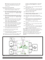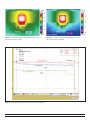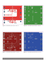
1
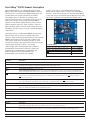
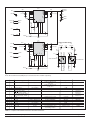
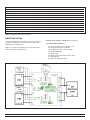
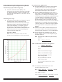
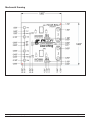
®
PI2125-EVAL2
Cool-ORing ™ Series
PI2125-EVAL2 Full-Function Active ORing
Evaluation Board User Guide
Cool-ORing™ Series
Contents
Introduction . . . . . . . . . . . . . . . . . . . . . . . . . . . . . . Page 1
PI2125 Product Description . . . . . . . . . . . . . . . . . . Page 2
Evaluation Board Terminal Description . . . . . . . . Page 2
Evaluation Board Schematic . . . . . . . . . . . . . . . . . Page 3
Bill of Materials . . . . . . . . . . . . . . . . . . . . . . . . . . . Page 3
Evaluation Board Configuration . . . . . . . . . . . . . . Page 4
Test Procedure . . . . . . . . . . . . . . . . . . . . . . . . . . . . Page 4
Thermal Images . . . . . . . . . . . . . . . . . . . . . . . . . . . Page 9
PCB Layouts . . . . . . . . . . . . . . . . . . . . . . . . . . . . . Page 10
Evaluation Board Mechanical Drawing . . . . . . . Page 11
The PI2125-EVAL2 Evaluation Board is intended to acquaint the
user with the benefits and features of the Cool-ORingTM PI2125
full function Active ORing solution. It is not designed to be
installed in end-use equipment.
Please read this document before setting up the PI2125-EVAL2
Evaluation Board and refer to the PI2125 product datasheet for
device specifications, functional description and characteristics.
PI2125-EVAL2 Evaluation Board
featuring the Cool-ORing PI2125
Full-Function Active ORing Solution.
During operation, the power devices and surrounding
structures can be operated safely at high temperatures.
• Remove power and use caution when connecting and
disconnecting test probes and interface lines to avoid
inadvertent short circuits and contact with hot surfaces.
• When testing electronic products always use approved
safety glasses. Follow good laboratory practice and
procedures.
Introduction
The PI2125-EVAL2 allows the user to test the basic principle
and operational characteristics of an Active ORing function in
a redundant power architecture, while also experiencing the
benefits and value of the PI2125 solution versus conventional
Active ORing solutions. The PI2125-EVAL2 evaluation board is
configured to receive two independent power source inputs,
per a typical redundant power architecture, through two
Active ORing channels that are combined to form a
redundant power output. Each channel is capable of up to
12 A, and is suitable for redundant bus voltages up to 12 V.
For high current Active ORing, above 12 A, the two channels
provided on the evaluation board can be paralleled in a
master/slave configuration and OR’d with a second
evaluation board.
Picor Corporation • www.picorpower.com
The PI2125-EVAL2 evaluation board is designed with
optimized PCB layout and component placement to represent
a realistic high density final design for an embedded Active
ORing solution for ≤ 12 Vbus applications requiring up to
12 A. This evaluation board is intended as an easy and simple
way to test the electrical and thermal performance of the
PI2125 Full-Function Active ORing solution.
Both dynamic and steady state testing of the PI2125 can be
completed on the PI2125-EVAL2 evaluation board, in addition
to using the key features of the product. Dynamic testing can
be completed under a variety of system level fault conditions
to check for response time to faults.
This document provides basic instructions for initial start-up
and configuration of the evaluation board. Further
information on the functionality of the PI2125 can be
found in the PI2125 product datasheet.
PI2125-EVAL2 User Guide Rev. 1.1 Page 1 of 11
Cool-ORingTM PI2125 Product Description
The Cool-ORing PI2125 is a complete full-function Active
ORing solution with a high-speed ORing MOSFET controller
and a very low on-state resistance MOSFET designed for use
in redundant power system architectures. The PI2125
Cool-ORing solution is offered in an extremely small,
thermally enhanced 5 mm x 7 mm LGA package and can be
used in low voltage (≤ 12 Vbus) high side Active ORing
applications. The PI2125 enables extremely low power loss
with fast dynamic response to fault conditions, critical for
high availability systems. A master / slave feature allows the
paralleling of PI2125 solutions for high current Active ORing
requirements.
The PI2125, with its 5.5 mΩ internal MOSFET provides very
high efficiency and low power loss during steady state
operation, while achieving high-speed turn-off of the internal
MOSFET during input power source fault conditions that
cause reverse current flow. The PI2125 provides an active
low fault flag output to the system during excessive forward
current, light load, reverse current, over-voltage,
under-voltage, and over-temperature fault conditions.
A temperature sensing function indicates a fault if the
maximum junction temperature exceeds 160°C. The
under-voltage and over-voltage thresholds are
programmable via an external resistor divider.
Figure 1 shows a photo of the PI2125-EVAL2 evaluation
board, with two PI2125 used to form the two Active ORing
channels. The board is built with two identical Active ORing
circuits with options and features that enable the user to fully
explore the capabilities of the PI2125 Cool-ORing solution.
Terminals Rating
Vin1, Vin2
20V / 12A
Vaux1 - Vin1 (R2 = 10Ω) see Vaux section
-0.3V to 17.3V/40mA
Vaux2 - Vin2 (R4= 10Ω) see Vaux section
-0.3V to 17.3V/40mA
SLI - Vin1
-0.3V to 8.0V/ 10mA
SL2 - Vin2
-0.3V to 8.0V/ 10mA
Figure 1: PI2125-EVAL2 Evaluation Board (1.8” x 1.8”)
Terminal
Description
Vin1
Power Source Input #1 or bus input designed to accommodate up to 12A continuous current.
Vaux1
Auxiliary Input Voltage #1 to supply PI2125 (SIP1) VC power. If Vaux1 is referenced to Gnd, Vaux1 should equal
Vin1 plus 5.5 V or higher. See details in the Auxiliary Power Supply (Vaux) section.
Rtn1
Vaux1 Return Connection: Connected to Vin1
Gnd
Vin & Vout Return Connection: Three Gnd connections are available and are connected to a common point, the Ground
plane. Input supplies Vin1 & Vin2 and the output load at Vout should all be connected to their respective local Gnd connection.
SL1
PI2125 (SIP1) Slave Input-Output pin: : For monitoring SIP1 slave pin. When SIP1 is configured as the Master, this pin
functions as an output that drives slaved PI2125 devices. When SIP1 is configured in Slave mode, SL1 serves as an input.
SL1 is referenced to Vin1.
SL2
PI2125 (SIP2) Slave Input-Output pin: For monitoring SIP2 slave pin. When SIP2 is configured as the Master, this pin functions
as an output that drives slaved PI2125 devices. When SIP2 is configured in Slave mode, SL2 serves as an input.
Vin2
Power Source Input #2 or bus input designed to accommodate up to 12 A continuous current.
Vaux2
Auxiliary Input Voltage #2 to supply SIP2 VC power. If Vaux2 is referenced to Gnd, Vaux2 should equal Vin2 plus 5.5 V or
higher. See details in the Auxiliary Power Supply (Vaux) section.
Rtn2
Vaux2 Return Connection: Connected to Vin2
FT1
PI2125 (SIP1) Fault pin: Monitors SIP1 fault conditions and level shifted to be referenced to the Gnd terminal
FT2
PI2125 (SIP2) Fault pin: Monitors SIP2 fault conditions and level shifted to be referenced to the Gnd terminal
Vout
Output: SiP1 and SiP2 D pins connection, connect to the load high side.
Table 1 – PI2125-EVAL2 Evaluation Board Terminals Description
Jumper
J1, J3
J2
Description
BK Jumpers: Connect jumper across M for master mode and across S for slave mode. Remove jumper to adjust reverse fault
blanking time using Rbk, Rbk is R3 for SIP1 and R6 for SIP2 shown in the schematic, Figure 2.
Slave Jumper: Remove the jumper unless one of the PI2125 is configured in slave mode. Since SIP1 and SIP2 returns are
referenced to Vin1 and Vin2, Slave should be used only when Vin1 and Vin2 are connected to the same input source.
Table 2 – PI2125-EVAL2 Evaluation Board jumpers description
Picor Corporation • www.picorpower.com
PI2125-EVAL2 User Guide Rev. 1.1 Page 2 of 11
SIP1
PI2125
Vin1
2
3
4
5
C4
Un-installed
6
Gnd
Gnd3
Gnd4
OV
GND
C3
22 uF
12
VC
11
VC1
Vin1
SL
BK
Vaux1
Rtn1
8
Vaux1
Vout2
C6
Un-installed
13
UV
FT
Vout1
Vout
14
SN
SP
7
FT1
1
17
16
15
D
D
D
D
10
Gnd
S
S
S
S
9
Vin1
J1
SL1
SL1
SL1
R3
C1
J2
SL2
SL2
1 uF
R4
Vaux1
10 Ω
VC1
SIP2
PI2125
R5
10K
R2
10K
13
Flt1
VC1
VC2 Flt2
6
5
Q1
NSBC114EPDXV6T1
J3
FT2
R1
4
5
R1
R2
6
FT1
12
8
VC2
Vin2
Rtn2
D2
Red LED
Vout
14
OV
BK
Vaux2
D1
Red LED
C7
Un-installed
R2
UV
Fault Level Shift Circuit
1
17
16
15
4
SN
FT
GND
Vaux2
SP
7
11
FT2
6
VC
Gnd
D
D
D
D
10
Gnd
S
S
S
S
SL
C5
Un-installed
2
3
4
5
9
Vin2
Vin2
Q2
NSBC114EPDXV6T1
1
R2
R1
2
3
3
R1
R8
R9
1 uF
R7
Vaux2
1
C2
2
R2
SL2
R6
10 Ω
VC2
Figure 2 – PI2125-EVAL2 Evaluation Board schematic.
Note: SIP1 and SIP2 returns (GND pins) are referenced to Vin1 and Vin2 respectively.
Item
QTY
Reference Designator
Value
1
2
C1, C2
1 µF
2
1
C3
22 µF
3
4
4
2
5
8
6
7
7
8
9
10
11
12
13
2
1
2
2
2
2
2
C4, C5, C6, C7
D1, D2
FT1, FT2, Rtn1, Rtn2,
SL1, SL2, Vaux1, Vaux2
Gnd1, Gnd2, Gnd3, Gnd4,
Vin1, Vin2, Vout1, Vout2
J1, J3
J2
Q1, Q2
R2, R5, R8, R9
R3, R6
R4, R7
SiP1, SiP2
Description
Capacitor, MLCC X5R,
1 µF,16 V
Capacitor, MLCC X7R,
22 µF, 25 V
Not installed
NSBC114EPDXV6 T1
10 KΩ
Not Installed
10 Ω
PI2125
Footprint
0603
1210
LED, Super Red
1206
THIN 0603
Turret Test point
TURRET-1528
Turret Test point
TURRET-1502
Header Pins 0.1" pitch
Header Pins 0.1" pitch
Pre-Biased NPN-PNP
Resistor,10 Ω,5%
2 x 3mm
2 x 2mm
SOT-563
0603
0603
0603
5x7mm;17 pins
Resistor,10Ω,5%
Picor Full-Function 12 A
Cool-ORing Solution
Manufacturer
Lite-On, Inc.,
Keystone
Electronics
Keystone
Electronics
ON Semi
PICOR
Table 3 – Complete PI2125-EVAL2 Evaluation Board Bill of Material
Picor Corporation • www.picorpower.com
PI2125-EVAL2 User Guide Rev. 1.1 Page 3 of 11
Reference Designator
Value
C1, C2
1 µF
C3
22 µF
C4, C5, C6, C7
Not installed
D1, D2
LED
Functional Description
VC Bypass Capacitor
Output (Load) Capacitor
Snubber to reduce voltage ringing when the device turns off
To indicate a fault exist when it is on
J1, J3
Jumper
To select between Master and Slave Modes
J2
Jumper
Connection between SL1 and SL2
Q1, Q2
NSBC114EPDXV6 T1
Fault level shift circuit
R2, R5,
10 KΩ
R9, R8
10 KΩ
R3, R6
Not Installed
R4, R7
10 Ω
VC Bias Resistor
PI2125
Cool-ORing SiP.
SiP1, SiP2
LED Current Limiter
Fault level shift gate bias resistor
BK Delay Timer Programmable Resistor
Table 4 – Component functional description
Initial Test Set Up
To test the PI2125-EVAL2 evaluation board it is necessary to
configure the jumpers (J1, J2 and J3) first based on the
required board configuration.
Failure to configure the jumper prior to the testing may
result in improper circuit behavior.
Baseline Test Procedure – PI2125 (Refer to Figure 3)
1.0 Recommended Equipment
1.1
1.2
1.3
1.4
1.5
1.6
1.7
1.8
Two DC power supplies - 0-20 V; 15 A.
DC power supply 12 V; 100 mA.
DC electronic load - 25 A minimum.
Digital Multimeter
Oscilloscope.
Appropriately sized interconnect cables.
Safety glasses.
PI2125 Product Data sheet.
Figure 3 – Layout configuration for typical redundant power application, using PI2125 with both solutions configured in Master Mode.
Picor Corporation • www.picorpower.com
PI2125-EVAL2 User Guide Rev. 1.1 Page 4 of 11
Before initial power-up follow these steps to configure the
evaluation board for specific end application requirements:
2.0 Undervoltage (UV) and Overvoltage (OV):
2.1 Since SIP1 and SIP2 are return (GND pin 11)
referenced to Vin1 and Vin2 respectively, UV and OV
are disabled. The UV pin is directly connected to the
VC pin (pin 10) and the OV pin is connected to the SIP
return (pin 11)
3.0 Blanking timer setup:
3.1 The blanking timer provides noise filtering for typical
switching power conversion that might cause
premature reverse current detection by masking the
reverse fault condition. The shortest blanking time
is 50 ns when the BK pin is connected to ground.
Connecting an external resistor (RBK, reference
designators R3 for SIP1 and R6 for SIP2) between the
BK pin and ground will increase the blanking time
as shown in the following chart.
Where: RBK ≤ 200 KΩ
Note: When BK is connected to VC for slave mode
operation, then the blanking time will be 270ns typically.
4.0 Auxiliary Power Supply (Vaux):
4.1 The PI2125 ORing SiP has a separate input (VC) that
provides power to the control circuitry and the
internal gate driver. An internal voltage regulator
(VC) clamps the VC voltage to 15.5 V typically.
4.2 Connect independent (Auxiliary) power sources to
Vaux inputs of the PI2125-EVAL2 Evaluation Board to
supply power to the VC input. The auxiliary power
source return can be connected to either Rtn terminal
or to Gnd terminal. If the auxiliary power source
return is connected to the Rtn terminal, make sure
that the auxiliary power source return is floating at
the source and will not cause a short circuit to the Vin
supply when it is connected to the positive terminal
of the Vin supply source. The Vaux voltage should be
5.5 V higher than Vin to fully enhance the internal
MOSFET.
4.3 10 Ω bias resistors (Rbias, reference designators R4
and R7) are installed on the PI2125-EVAL2 between
each Vaux input and VC pin of one of the PI2125 SiPs.
4.4 If Vaux is higher than the Clamp voltage, 15.5 V
typical, the Rbias value has to be changed using the
following equations:
4.4.1 Select the value of Rbias using the following
equation:
Rbias =
4.4.2
Vauxmin – VCclampMAX
ICmax
Calculate Rbias maximum power dissipation:
PdRbias =
(Vauxmax – VCclampMIN)2
Rbias
Where:
Vauxmin: Vaux minimum voltage
Vauxmax: Vaux maximum voltage
VCClampMAX: Maximum controller
clamp voltage, 16.0 V
VCClampMIN: Minimum controller
clamp voltage, 14.0 V
ICmax: Controller maximum bias current,
use 4.2 mA
4.4.3 For example, if the minimum Vaux = 22 V
and the maximum Vaux = 26 V
Rbias =
Vauxmin – VCclampMAX
ICmax
=
22 V–16 V
= 1.429 KΩ
4.2 mA
use 1.43 KΩ 1% resistor
PdRbias = (Vauxmax – VCclampMIN)2 = (28 V–14.0 V)2 = 137 mW
Rbias
1.43 KΩ
Picor Corporation • www.picorpower.com
PI2125-EVAL2 User Guide Rev. 1.1 Page 5 of 11
Note: Minimize the resistor value for low Vaux voltage
levels to avoid a voltage drop that may reduce the VC
voltage lower than required to drive the gate of the
internal MOSFET.
5.0 Hook Up of the Evaluation Board
5.1 Verify that the jumpers J1 and J3 are installed for
master mode [across M] and no Jumper on J2.
5.2 Connect the positive terminal of PS1 power supply to
Vin1. Connect the ground terminal of PS1 to its local
Gnd. Set the power supply to 12 V. Keep PS1 output
disabled, off.
5.3 Connect the positive terminal of PS2 power supply to
Vin2. Connect the ground terminal of PS2 to its local
Gnd. Set the power supply to 12 V. Keep PS2 output
disabled, off.
5.4 Connect the positive terminal of PS3 power supply to
Vaux1. Connect the ground terminal of this power
supply to Rtn1. Set the power supply to 12 V or
higher. Keep PS3 output disabled, off.
5.5 Connect the positive terminal of PS4 power supply to
Vaux2. Connect the ground terminal of this power
supply to Rtn2. Set the power supply to 12 V or
higher. Keep PS4 output disabled, off.
5.6 Connect the electronic load to the output between
Vout and Gnd. Set the load current to 5 A.
5.7 Enable (turn on) PS1 power supply output.
5.8 Turn on the electronic load.
5.9 Verify that the electronic load input voltage reading
is one diode voltage drop below 12V.
5.10 Enable (turn on) PS3 and PS4 power supplies output.
5.11 Verify that the electronic load voltage reading
increases to a few millivolts below 12 V. This verifies
that the PI2125 internal MOSFET is in conduction
mode.
5.12 Verify that Vin2 is at 0 V. This verifies that the PI2125
(SIP2) internal FET is off.
5.13 D2 should be on. This is due to a reverse voltage fault
condition caused by the bus voltage being high with
respect to the input voltage (Vin2).
5.14 Enable (turn on) PS2 output.
5.15 Verify that both PS1 and PS2 are sharing load current
evenly by looking at the supply current.
5.16 Disable (turn off) PS1, PS2, PS3 and PS4 outputs.
5.17 Enable (turn on) PS2 output then Enable PS3 and PS4
outputs.
5.18 Verify that the electronic load voltage reading is few
millivolts below 12 V. This verifies that the PI2125
internal MOSFET is in conduction mode.
5.19 D2 should be off. This verifies that there is no fault
condition.
5.20 Verify that Vin1 is at 0 V. This verifies that the PI2125
(SIP1) internal FET is off.
5.21 D1 should be on. This is due to a reverse voltage fault
condition caused by the bus voltage being high with
respect to the input voltage (Vin1).
6.0 Slave Mode: Slave Mode can be demonstrated in two
setups; either by using one PI2125-EVAL2 evaluation board as
a single ORing function with both PI2125 effectively in
parallel or two PI2125-EVAL2 evaluation boards to
demonstrate a true redundant 20 A system. The following
test steps uses a single PI2125-EVAL2 in a slave mode
application.
Figure 4: Layout configuration for typical application, SiP1 in Master Mode and SiP2 Slave Mode
Picor Corporation • www.picorpower.com
PI2125-EVAL2 User Guide Rev. 1.1 Page 6 of 11
Note: In this experiment SiP 1 is set in master mode and SiP2 in
slave mode.
6.1 As shown in figure 4, BK pin (J1) of the master device
will be connected to ground [across M] while the
slaved device BK pin (J3) is connected to VCC
[across S]. Place a jumper across J2 to connect slave
pins together.
6.2 Connect the positive terminal of PS1 power supply to
Vin1. Connect the ground terminal of this power
supply to Gnd. Set the power supply to 12 V. Keep
PS1 output disabled, off.
6.3 Connect the positive terminal of PS2 power supply to
Vin2. Connect the ground terminal of this power
supply to Gnd. Set the power supply to 12 V. Keep
PS2 output disabled, off.
6.4 Connect the positive terminal of PS3 power supply to
Vaux1. Connect the ground terminal of this power
supply to Rtn1. Set the power supply to 12 V. Keep
PS3 output disabled, off.
6.5 Connect the positive terminal of PS4 power supply to
Vaux2. Connect the ground terminal of this power
supply to Rtn2. Set the power supply to 12 V.
Keep PS4 output disabled, off.
6.6 Connect the electronic load between Vout and Gnd.
Set the load current to 10 A.
6.7 Enable (Turn on) PS2, PS3 and PS4 outputs, and keep
PS1 output disabled (off).
6.8 Turn on the electronic load.
6.9 Verify that electronic load voltage drops to a diode
drop below PS2. This verifies that the SIP2 internal
FET is off due to the Master (SIP1) not being on.
sourced from the evaluation board output through
the ORing internal MOSFET. The reverse current in
the MOSFET may reach over 60A in some conditions
before the MOSFET is turned off. Such high current
conditions will store high energy even in a small
parasitic element, and can be represented as ½Li2. A
1nH parasitic with 60A reverse current will generate
1.8µJ. When the MOSFET is turned off, the stored
energy will be released and will produce a high
negative voltage at the MOSFET source and high
positive voltage at the MOSFET drain. This event will
create a high voltage difference across the drain and
source of the MOSFET.
7.3 Apply a short at one of the inputs (Vin1 or Vin2)
when the evaluation board is configured with both
SIP’s (SIP1 and SIP2) in master mode. The short can be
applied electronically using a MOSFET connected
between Vin and Gnd or simply a by connecting Vin
to Gnd. Then measure the response time between
when the short is applied and the SIP internal
MOSFET is disconnected (or turned off). An example
for PI2125 response time to an input short circuit is
shown in Figure 5.
8.0 Internal MOSFET Rds(on) Measurement:
8.1 The SIP1 internal MOSFET Rds(on) can be measured
with a voltmeter between the S1 and D1 Kelvin
connection. The potential between S1 and D1 is the
voltage drop across the internal MOSFET and:
Rds(on) =
6.10 Enable (turn on) PS1 output:
6.11 Verify that the electronic load input voltage reading
is a few millivolts below 3.3 V and PS1 and PS2 are
sharing the load current evenly. This verifies that both
internal MOSFET’s of SiP1 and SiP2 are in conduction
mode.
7.0 Input short circuit test: before set-up is completed
consider the following:
VS1 – VD1
Iin
Where:
VS1–VD1: Voltage drop across the internal MOSFET
Iin: Input current.
Note: The value is temperature dependent and the .
junction temperature increases directly proportional to
power dissipation.
7.1 To emulate a real application, the BUS supplies for
this test should have a solid output source such as a
DC-DC converter that supplies high current and can
be connected very close to the evaluation board to
reduce stray parasitic inductance. Or use the
prospective supply sources of the end application
where the PI2125 will be used.
7.2 Stray parasitic inductance in the circuit can contribute
to significant voltage transient conditions, particularly
when the internal MOSFET is turned-off after a
reverse current fault has been detected. When a short
is applied at the output of the power sources and the
evaluation board input (Vin), a large reverse current is
Picor Corporation • www.picorpower.com
PI2125-EVAL2 User Guide Rev. 1.1 Page 7 of 11
Figure 6a – PI2125 mounted on PI2125-EVAL2, Iout = 12 A,
TA = 25°C, Air Flow = 0 LFM
Figure 6b – PI2125 mounted on PI2125-EVAL2, Iout = 12 A,
TA = 25°C, Air Flow = 200 LFM
Figure 5 – Plot of PI2125 response time to reverse current detection
Picor Corporation • www.picorpower.com
PI2125-EVAL2 User Guide Rev. 1.1 Page 8 of 11
Figure 7a – PI2125-EVAL2 layout top layer. Scale 2.0:1
Figure 7c – PI2125-EVAL2 layout mid layer 1. Scale 2.0:1
Picor Corporation • www.picorpower.com
Figure 7b – – PI2125-EVAL2 layout mid layer 2. Scale 2.0:1
Figure 7d –– PI2125-EVAL2 layout Bottom layer. Scale 2.0:1
PI2125-EVAL2 User Guide Rev. 1.1 Page 9 of 11
Mechancial Drawing
Picor Corporation • www.picorpower.com
PI2125-EVAL2 User Guide Rev. 1.1 Page 10 of 11
Vicor’s comprehensive line of power solutions includes high-density AC-DC & DC-DC
modules and accessory components, fully configurable AC-DC & DC-DC power supplies,
and complete custom power systems.
Information furnished by Vicor is believed to be accurate and reliable. However, no responsibility
is assumed by Vicor for its use. No license is granted by implication or otherwise under any patent
or patent rights of Vicor. Vicor components are not designed to be used in applications, such as
life support systems, wherein a failure or malfunction could result in injury or death. All sales are
subject to Vicor’s Terms and Conditions of Sale, which are available upon request.
Specifications are subject to change without notice.
Vicor Corporation
25 Frontage Road
Andover, MA 01810
USA
Picor Corporation
51 Industrial Drive
North Smithfield, RI 02896
USA
Customer Service: [email protected]
Technical Support: [email protected]
Tel: 800-735-6200
Fax: 978-475-6715
Picor Corporation • www.picorpower.com
PI2125-EVAL2 User Guide Rev. 1.1 4/09