1
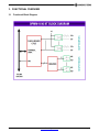
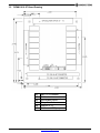
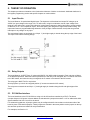
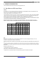
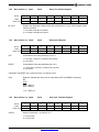
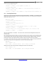
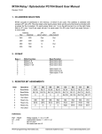
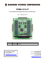
init
OPMM-1616-XT
PC/104 I/O Module with Optoisolated inputs and Relay Outputs
Rev 1.0 September 2010
Revision
Date
Comment
1.0
9/26/2010
first release
FOR TECHNICAL SUPPORT
PLEASE CONTACT:
[email protected]
Copyright 2010
Diamond Systems Corporation
1255 Terra Bella Ave.
Mountain View, CA 94043 USA
Tel 1-650-810-2500
Fax 1-650-810-2525
www.diamondsystems.com
CONTENTS
1.
2.
Important Safe Handling Information .............................................................................................................3
Introduction .......................................................................................................................................................4
2.1 Description .....................................................................................................................................................4
2.2 Features .........................................................................................................................................................4
3. Functional Overview .........................................................................................................................................5
3.1 Functional Block Diagram ..............................................................................................................................5
3.2 OPMM-1616-XT Board Drawing....................................................................................................................6
4. Connector Pinout and Pin Description ...........................................................................................................7
4.1 PC/104 (J1, J2) ..............................................................................................................................................7
4.2 Input (J3)........................................................................................................................................................7
4.3 Output (J4, J5) ...............................................................................................................................................8
5. Theory of Operation..........................................................................................................................................9
5.1 Input Circuits ..................................................................................................................................................9
5.2 Relay Outputs ................................................................................................................................................9
5.3 PC/104 Bus Interface ....................................................................................................................................9
5.4 Interrupts ..................................................................................................................................................... 10
5.5 LED Indicator .............................................................................................................................................. 10
6. Board Configuration ...................................................................................................................................... 11
6.1 Base Address and IRQ Jumper Settings .................................................................................................... 11
7. I/O Registers ................................................................................................................................................... 12
7.1 I/O Map Summary....................................................................................................................................... 12
7.2 I/O Register Details .................................................................................................................................... 13
7.2.1
Base address + 0 (0x00) Write Relay 7-0 Control Register ............................................................ 13
7.2.2
Base address + 0 (0x00) Read Relay 7-0 Status Register .............................................................. 13
7.2.3
Base address + 1 (0x01) Write Relay 15-8 Control Register .......................................................... 13
7.2.4
Base address + 1 (0x01) Read Relay 15 to 8 Status Register ........................................................ 14
7.2.5
Base address + 2 (0x02) Write Relay Select Register .................................................................... 14
7.2.6
Base address + 2 (0x02) Read Optoinput 7-0 Status Register ....................................................... 14
7.2.7
Base address + 3 (0x03) Write Board Reset Control Register ........................................................ 15
7.2.8
Base address + 3 (0x03) Read Optoinput 15-8 Status Register ..................................................... 15
7.2.9
Base address + 4 (0x04) Write Interrupt Control Register .............................................................. 15
7.2.10 Base address + 4 (0x04) Read Change Detect 7-0 Status Register ............................................... 16
7.2.11 Base address + 5 (0x05) Write LED Control Register ..................................................................... 16
7.2.12 Base address + 5 (0x05) Read Change Detect 15-8 Status Register ............................................. 16
8. Programming .................................................................................................................................................. 17
8.1 General Information .................................................................................................................................... 17
8.2 Reading an Opto Input ............................................................................................................................... 17
8.3 Turning Relays On and Off ......................................................................................................................... 18
8.3.1
Controlling Individual Relays ............................................................................................................. 18
8.3.2
Controlling Multiple Relays ................................................................................................................ 19
8.4 Interrupts ..................................................................................................................................................... 20
8.5 Other Software Commands ........................................................................................................................ 20
9. Specifications................................................................................................................................................. 21
OPMM-1616-XT User Manual Rev 1.0
www.diamondsystems.com
Page 2
1. IMPORTANT SAFE HANDLING INFORMATION
WARNING!
ESD-Sensitive Electronic Equipment
Observe ESD-safe handling procedures when working with this product.
Always use this product in a properly grounded work area and wear appropriate
ESD-preventive clothing and/or accessories.
Always store this product in ESD-protective packaging when not in use.
Safe Handling Precautions
This board contains a high density connector with many connections to sensitive electronic components. This
creates many opportunities for accidental damage during handling, installation and connection to other
equipment. The list here describes common causes of failure found on boards returned to Diamond Systems for
repair. This information is provided as a source of advice to help you prevent damaging your Diamond (or any
vendor’s) embedded computer boards.
ESD damage – This type of damage is usually almost impossible to detect, because there is no visual sign of
failure or damage. The symptom is that the board eventually simply stops working, because some component
becomes defective. Usually the failure can be identified and the chip can be replaced. To prevent ESD damage,
always follow proper ESD-prevention practices when handling computer boards.
Damage during handling or storage – On some boards we have noticed physical damage from mishandling. A
common observation is that a screwdriver slipped while installing the board, causing a gouge in the PCB surface
and cutting signal traces or damaging components.
Another common observation is damaged board corners, indicating the board was dropped. This may or may not
cause damage to the circuitry, depending on what is near the corner. Most of our boards are designed with at
least 25 mils clearance between the board edge and any component pad, and ground / power planes are at least
20 mils from the edge to avoid possible shorting from this type of damage. However these design rules are not
sufficient to prevent damage in all situations.
A third cause of failure is when a metal screwdriver tip slips, or a screw drops onto the board while it is powered
on, causing a short between a power pin and a signal pin on a component. This can cause overvoltage / power
supply problems described below. To avoid this type of failure, only perform assembly operations when the
system is powered off.
Sometimes boards are stored in racks with slots that grip the edge of the board. This is a common practice for
board manufacturers. However our boards are generally very dense, and if the board has components very close
to the board edge, they can be damaged or even knocked off the board when the board tilts back in the rack.
Diamond recommends that all our boards be stored only in individual ESD-safe packaging. If multiple boards are
stored together, they should be contained in bins with dividers between boards. Do not pile boards on top of each
other or cram too many boards into a small location. This can cause damage to connector pins or fragile
components.
Power supply wired backwards – Our power supplies and boards are not designed to withstand a reverse
power supply connection. This will destroy each IC that is connected to the power supply (i.e. almost all ICs). In
this case the board will most likely will be unrepairable and must be replaced. A chip destroyed by reverse power
or by excessive power will often have a visible hole on the top or show some deformation on the top surface due
to vaporization inside the package. Check twice before applying power!
Overvoltage on digital I/O line – If a digital I/O signal is connected to a voltage above the maximum specified
voltage, the digital circuitry can be damaged. On most of our boards the acceptable range of voltages connected
to digital I/O signals is 0-5V, and they can withstand about 0.5V beyond that (-0.5 to 5.5V) before being damaged.
However logic signals at 12V and even 24V are common, and if one of these is connected to a 5V logic chip, the
chip will be damaged, and the damage could even extend past that chip to others in the circuit
OPMM-1616-XT User Manual Rev 1.0
www.diamondsystems.com
Page 3
2. INTRODUCTION
2.1
Description
OPMM-1616-XT is a PC/104 I/O module with 16 optoisolated inputs and 16 relay outputs.
2.2
Features
Optoisolated Inputs
16 unidirectional optoisolated inputs with current limiting resistors
30VDC input capacity
0-1.5V input = logic 0; 3-30VDC input = logic 1
Programmable edge detection with interrupts
Relay Outputs
16 relay outputs
Form C contacts (SPDT)
2A current capacity
30VDC / 30W switching capacity
Bus Interface
PC/104 8-bit ISA bus interface (both 8-bit and 16-bit connectors installed)
8 byte I/O footprint
IRQ support
Environmental / Mechanical
PC/104 format board
o
o
-40 C to +85 C operating temperature
+5VDC input voltage
OPMM-1616-XT User Manual Rev 1.0
www.diamondsystems.com
Page 4
3. FUNCTIONAL OVERVIEW
3.1
Functional Block Diagram
OPMM-1616-XT User Manual Rev 1.0
www.diamondsystems.com
Page 5
3.2
OPMM-1616-XT Board Drawing
J1
J2
J3
J4
J5
J6
OPMM-1616-XT User Manual Rev 1.0
Main PC/104 header
16-bit extension
Optoisolated inputs
Relays 0 to 7
Relays 8 to 15
Address and IRQ jumpers
www.diamondsystems.com
Page 6
4. CONNECTOR PINOUT AND PIN DESCRIPTION
4.1
PC/104 (J1, J2)
Connectors J1 (PC/104) and J2 (16-bit extension) provide connection to the motherboard.
4.2
Input (J3)
Connector J3 handles optoisolated inputs.
In 0+
In 1+
In 2+
In 3+
In 4+
In 5+
In 6+
In 7+
In 8+
In 9+
In 10+
In 11+
In 12+
In 13+
In 14+
In 15+
NC
J3: Input
1
2
3
4
5
6
7
8
9 10
11 12
13 14
15 16
17 18
19 20
21 22
23 24
25 26
27 28
29 30
31 32
33 34
In 0In 1In 2In 3In 4In 5In 6In 7In 8In 9In 10In 11In 12In 13In 14In 15NC
Connector type: 0.1” pitch 34-pin dual row right-angle pin header
Signal Name
In n+
In nNC
Definition
High side of optoisolated input
Low side of optoisolated input
Unused pin
OPMM-1616-XT User Manual Rev 1.0
www.diamondsystems.com
Page 7
4.3
Output (J4, J5)
Connectors J4, at the right edge of the board, and J5, at the left edge, handle outputs.
Relay 0 NO
Relay 0 NC
Relay 1 C
Relay 2 NO
Relay 2 NC
Relay 3 C
Relay 4 NO
Relay 4 NC
Relay 5 C
Relay 6 NO
Relay 6 NC
Relay 7 C
NC
J4: Relays 0 - 7
1
2
Relay 0 C
3
4
Relay 1 NO
5
6
Relay 1 NC
7
8
Relay 2 C
9
10
Relay 3 NO
11
12
Relay 3 NC
13
14
Relay 4 C
15
16
Relay 5 NO
17
18
Relay 5 NC
19
20
Relay 6 C
21
22
Relay 7 NO
23
24
Relay 7 NC
25
26
NC
Connector type: 0.1” pitch 34-pin dual
row right-angle pin header
Signal Name
Relay n NO
Relay n C
Relay n NC
NC
J5: Relays 8 - 15
Relay 8 NO
1
2
Relay 8 C
Relay 8 NC
3
4
Relay 9 NO
Relay 9 C
5
6
Relay 9 NC
Relay 10 NO
7
8
Relay 10 C
Relay 10 NC
9
10 Relay 11 NO
Relay 11 C 11
12 Relay 11 NC
Relay 12 NO 13
14 Relay 12 C
Relay 12 NC 15
16 Relay 13 NO
Relay 13 C 17
18 Relay 13 NC
Relay 14 NO 19
20 Relay 14 C
Relay 14 NC 21
22 Relay 15 NO
Relay 15 C 23
24 Relay 15 NC
NC 25
26 NC
Connector type: 0.1” pitch 34-pin dual
row right-angle pin header
Definition
Normally open contact (disconnected when power off or relay de-energized,
connected to Common contact when relay energized)
Common contact
Normally closed contact (connected to Common contact when power off or relay
de-energized, disconnected when relay energized)
Unused pin
OPMM-1616-XT User Manual Rev 1.0
www.diamondsystems.com
Page 8
5. THEORY OF OPERATION
This chapter provides an orientation to the functional architecture of blocks on the board. Additional details are in
the register programming section and specific chapters on various blocks.
5.1
Input Circuits
The board features 16 optoisolated digital inputs. The inputs are unidirectional and accept DC voltages up to
30VDC. An input voltage in the range of 0-1.5V will result in a logic low indication, and an input voltage in the
range of 3-30V will result in a logic high indication. Inputs feature channel to channel and input to output isolation
of 500V DC or AC. The components, layout, and trace spacing are designed to support this isolation rating. The
inputs also feature a programmable edge detection circuit (change of state detection circuit) that can generate
interrupts on any change on any input.
The optoisolated inputs are accessed via a 34-pin .1” pitch right-angle pin header along the top edge of the board.
The input circuit has the following design:
5.2
Relay Outputs
The board features 16 DPDT (form C) relays with 30VDC / 2A (60W resistive) capacity. Each relay has a lifetime
of 10,000,000 operations. When the board is powered off or the relay is de-energized, the C contact is connected
to the NC contact, and when the relay is energized, the C contact is connected to the NO contact.
The relay type is NAIS TX2-5 or equivalent.
All relays power up in their de-energized position (C contact connected to NC contact).
The relays are accessed via two 26-pin .1” pitch right-angle pin headers along the left and right edges of the
board.
5.3
PC/104 Bus Interface
The board interfaces to the PC/104 ISA bus using an 8-bit I/O interface controlled by a CPLD. The board
occupies 8 bytes in I/O space. Its base address is selected with 6 jumpers that select 1 or 0 for address bits A9-4.
System address bits A15-10 are 0 for the board.
For enhanced ruggedness, all jumper options may be configured with 0-ohm resistors on the bottom side of the
board in place of mechanical jumpers. These jumpers are oriented in the same position as the jumpers on the top
side and their positions are labeled for easy identification.
For examples, see Section 6.1.
OPMM-1616-XT User Manual Rev 1.0
www.diamondsystems.com
Page 9
5.4
Interrupts
The design includes an interrupt circuit for generating ISA bus IRQs. The IRQ options are 3, 4, 5, 6, 7, 10, and 11.
An additional jumper enables selection of the 1K ohm pull-down resistor required for PC/104 IRQ sharing. IRQ10
and IRQ11 are on the 16-bit connector, while the remaining IRQs are on the 8-bit connector. Thus a board without
the 16-bit connector installed does not have access to IRQ10 and IRQ11.
For example, see Section 6.1.
5.5
LED Indicator
The board has one LED indicator, located to the right of J2, which turns ON upon power-up. The LED can be
controlled via software using a register write command as explained in the software section of this manual.
OPMM-1616-XT User Manual Rev 1.0
www.diamondsystems.com
Page 10
6. BOARD CONFIGURATION
The board address and interrupt values are set using jumpers on J6.
6.1
Base Address and IRQ Jumper Settings
Address
Pin positions on J6 in the address area labeled 9 through 4 are used together to select a base address for the
board. The six pin positions are identified in the table below.
A jumper plug in applies a 0 to that address bit, out is a 1.
The base address is always 12 bits long. The lower four address bits are always 0, which means that the OPMM1616-XT board can only be configured on 16 byte boundaries. Also, the upper 2 bits (address bit 10 and bit 11)
are also always zero which means that the maximum value in the MSB can only be 0011 or 3.
The valid address range is from 0x0100 to 0x3F0. A board shipped from the factory is at default address of 300H.
You may need to verify that this setting is compatible with your system.
NOTE: The table information only suggests some possible addresses. Others are possible as long as the
address is 100 hex or higher and the address range does not conflict with any other resource on the ISA bus.
Header label for address pins
Hex
Decimal
9
8
7
6
5
4
100
256
in
out
140
320
in
out
in
in
in
in
in
out
in
in
180
384
in
out
out
in
in
in
1C0
448
200
512
in
out
out
out
in
in
out
in
in
in
in
in
240
576
out
in
in
out
in
in
280
640
out
in
out
in
in
in
300 (default)
768
out
out
in
in
in
in
3F0
1016
out
out
out
in
in
in
IRQ
Pin positions in the IRQ section of J6 and which are labeled 15 to 3 are for setting the IRQ value. 'R' is for
selection of a 1kΩ pull-down resistor on the IRQ line.
To select an IRQ, place a jumper block at the position next to the number of the desired IRQ on the board next to
J6.
To enable a pull-down resistor on the IRQ line (if no other device on the bus has one enabled), place a jumper on
the 'R' position of J6. When using an IRQ, one (and only one) board in the system must have a pull-down resistor
on the line.
Examples of IRQ settings on J6:
To enable IRQ5, place a jumper at position 5.
Alternatively, to enable IRQ14, place a jumper at position 14.
To disable use of a pull-down resistor for this board's IRQ, position 'R' should be unoccupied.
OPMM-1616-XT User Manual Rev 1.0
www.diamondsystems.com
Page 11
7. I/O REGISTERS
7.1
I/O Map Summary
The board is controlled and monitored via eight 8-bit registers as defined below.
Write
Offset from
base
address
7
6
5
4
3
2
1
0
0
RLY7
RLY6
RLY5
RLY4
RLY3
RLY2
RLY1
RLY0
1
RLY15
RLY14
RLY13
RLY12
RLY11
RLY10
RLY9
RLY8
2
SET
RESET
R3
R2
R1
R0
3
BRDRST
INTE1
INTE0
INTRST
4
5
LED
6
7
Read
Offset
7
6
5
4
3
2
1
0
0
RLY7
RLY6
RLY5
RLY4
RLY3
RLY2
RLY1
RLY0
1
RLY15
RLY14
RLY13
RLY12
RLY11
RLY10
RLY9
RLY8
2
OPTO7
OPTO6
OPTO5
OPTO4
OPTO3
OPTO2
OPTO1
OPTO0
3
OPTO15
OPTO14
OPTO13
OPTO12
OPTO11
OPTO10
OPTO9
OPTO8
4
CHG7
CHG6
CHG5
CHG4
CHG3
CHG2
CHG1
CHG0
5
CHG15
CHG14
CHG13
CHG12
CHG11
CHG10
CHG9
CHG8
6
7
RLY15-0
Register bits: Controls the states of the 16 relays; the associated I/O pins match the value written
to the registers. These register values may be read back.
SET
Command bit: Sets relay defined by R3-0 to 1.
RESET
Command bit: Sets relay defined by R3-0 to 0.
R3-0
Data bits: Indicates the relay to set or reset with the SET and RESET commands.
BRDRST
Command bit: Resets all registers to 0.
INTRST
Command bit: Resets the interrupt request circuit but does not disable interrupts.
INTE1, 0
Register bits: Enables interrupt on change of state for relays 15-8 and 7-0, respectively.
LED
Register bit: Drives an on-board status LED.
OPTO15-0 Reads back the states of the 16 opto input pins.
CHG15-0
Reads back the current state of the input change detect circuit flip flops.
OPMM-1616-XT User Manual Rev 1.0
www.diamondsystems.com
Page 12
7.2
I/O Register Details
This section describes the location and general behavior of specific bits in each I/O map register. In all register
definitions below, any bit named X is not defined and serves no function.
7.2.1
Base address + 0 (0x00)
Write
Relay 7-0 Control Register
Bit No.
7
6
5
4
3
2
1
0
Name
RLY7
RLY6
RLY5
RLY4
RLY3
RLY2
RLY1
RLY0
Reset value
0
0
0
0
0
0
0
0
RLY0-7
Register bits controlling the states of the relays 7 to 0. These register values may be read
back.
1 = Contacts C and NC are closed.
0 = Contacts C and NO are closed.
7.2.2
Base address + 0 (0x00)
Read
Relay 7-0 Status Register
Bit No.
7
6
5
4
3
2
1
0
Name
RLY7
RLY6
RLY5
RLY4
RLY3
RLY2
RLY1
RLY0
Reset value
0
0
0
0
0
0
0
0
RLY0-7
Register bits showing the status of the relay control bits for 7 to 0.
1 = Contacts C and NC are closed.
0 = Contacts C and NO are closed.
7.2.3
Base address + 1 (0x01)
Write
Relay 15-8 Control Register
Bit No.
7
6
5
4
3
2
1
0
Name
RLY15
RLY14
RLY13
RLY12
RLY11
RLY10
RLY9
RLY8
Reset value
0
0
0
0
0
0
0
0
RLY8-15
Register bits controlling the states of the relays 15 to 8. These register values may be read
back.
1 = Contacts C and NC are closed.
0 = Contacts C and NO are closed.
OPMM-1616-XT User Manual Rev 1.0
www.diamondsystems.com
Page 13
7.2.4
Base address + 1 (0x01)
Read
Relay 15 to 8 Status Register
Bit No.
7
6
5
4
3
2
1
0
Name
RLY15
RLY14
RLY13
RLY12
RLY11
RLY10
RLY9
RLY8
Reset value
0
0
0
0
0
0
0
0
RLY8-15
Register bits showing the status of the relay control bits for 15 to 8. These register values
may be read back.
1 = Contacts C and NC are closed.
0 = Contacts C and NO are closed.
7.2.5
Base address + 2 (0x02)
Bit No.
7
6
Name
SET
RESET
Reset value
0
0
SET
Write
5
0
Relay Select Register
4
3
2
1
0
R3
R2
R1
R0
0
0
0
0
0
Command bit: Sets relay defined by R3-0 to 1.
1 = Set relay. (connect C contact to NO contact)
0 = No action.
RESET
Command bit: Clear relay defined by R3-0 to 0.
1 = Clear relay. (connect C contact to NC contact)
0 = No action.
If both SET and RESET are 1 at the same time, no change occurs.
R3-0
Data bits: Indicates the relay to set or reset with the SET and RESET commands.
BIT
3210
0000 = Relay 0.
0001 = Relay 1.
...
1111 = Relay 15.
7.2.6
Base address + 2 (0x02)
Read
Opto input 7-0 Status Register
Bit No.
7
6
5
4
3
2
1
0
Name
OPTO7
OPTO6
OPTO5
OPTO4
OPTO3
OPTO2
OPTO1
OPTO0
Reset value
0
0
0
0
0
0
0
0
OPTOn
Status of Opto input n. for inputs 7 to 0.
1 = input is high.
0 = input is low.
OPMM-1616-XT User Manual Rev 1.0
www.diamondsystems.com
Page 14
7.2.7
Base address + 3 (0x03)
Bit No.
7
Name
BRDRST
Reset value
0
BRDRST
6
Write
5
Board Reset Control Register
4
3
2
1
0
0
0
0
INTRST
0
0
0
0
Command bit: Reset all registers to 0
1 = reset all registers to 0.
0 = no action.
INTRST
Command bit: Resets the interrupt request circuit but does not disable interrupts.
1 = reset interrupt request and allow another interrupt.
0 = no action.
7.2.8
Base address + 3 (0x03)
Read
Opto input 15-8 Status Register
Bit No.
7
6
5
4
3
2
1
0
Name
OPTO15
OPTO14
OPTO13
OPTO12
OPTO11
OPTO10
OPTO9
OPTO8
Reset value
0
0
0
0
0
0
0
0
1
0
INTE1
INTE0
0
0
OPTOn
Status of Opto input n for inputs 15 to 8.
1 = input is high.
0 = input is low.
7.2.9
Base address + 4 (0x04)
Bit No.
7
6
Write
5
Interrupt Control Register
4
3
2
Name
Reset value
INTE1
0
0
0
0
0
0
Enables interrupt on change of state for opto inputs 15-8.
1 = enable interrupt on change of state.
0 = no action.
INTE0
Enables interrupt on change of state for opto inputs 7-0
1 = enable interrupt on change of state.
0 = no action.
OPMM-1616-XT User Manual Rev 1.0
www.diamondsystems.com
Page 15
7.2.10 Base address + 4 (0x04)
Read
Change Detect 7-0 Status Register
Bit No.
7
6
5
4
3
2
1
0
Name
CHG7
CHG6
CHG5
CHG4
CHG3
CHG2
CHG1
CHG0
Reset value
0
0
0
0
0
0
0
0
CHGn
Reads back the status of the change detect circuit for inputs 7-0.
1 = input has changed.
0 = input has not changed.
If INTE0=1, any change on inputs 7-0 will generate an IRQ. The change is indicated with a 1
in the corresponding bit CHG7-0. INTRST=1 is a command bit that resets all CHG bits and
the interrupt circuit but keeps the circuit enabled and ready if INTE0 =1.
7.2.11 Base address + 5 (0x05)
Bit No.
Write
LED Control Register
7
6
5
4
3
2
1
0
0
0
0
0
0
0
Name
Reset value
LED
0
LED
0
Drives an on-board status LED.
1 = LED On (default on power-up).
0 = LED Off.
7.2.12 Base address + 5 (0x05)
Read
Change Detect 15-8 Status Register
Bit No.
7
6
5
4
3
2
1
0
Name
CHG15
CHG14
CHG13
CHG12
CHG11
CHG10
CHG9
CHG8
Reset value
0
0
0
0
0
0
0
0
CHGn
Reads back the status of the change detect circuit for inputs 15-8.
1 = input has changed.
0 = input has not changed.
If INTE1=0, any change on inputs 15-8 will generate an IRQ. The change is indicated with a 1
in the corresponding bit CHG15-8. INTRST=1 is a command bit that resets all CHG bits and
the interrupt circuit but keeps the circuit enabled and ready if INTE1 =1.
OPMM-1616-XT User Manual Rev 1.0
www.diamondsystems.com
Page 16
8. PROGRAMMING
The OPMM-1616-XT functionality is simple to program, using either the Universal Driver version 7.00 or by
programming the board registers using simple register read/writes. This section describes how to program the
outputs and read the inputs in the C language.
8.1
General Information
All access to the board is done with I/O commands, meaning data is read and written to the computer’s I/O
memory as opposed to data memory or the keyboard or display.
To access the board in C, use the following code:
Input:
a = inp(addr);
Output:
outp(addr,a);
In the example, "a" is the data and "addr" is the I/O address of the board, as specified above in Board
Configuration.
8.2
Reading an Opto Input
The registers used to read an opto input are as shown in the table below.
Read
Offset from
base
address
7
6
5
4
3
2
1
0
Base + 2
OPTO7
OPTO6
OPTO5
OPTO4
OPTO3
OPTO2
OPTO1
OPTO0
Base + 3
OPTO15
OPTO14
OPTO13
OPTO12
OPTO11
OPTO10
OPTO9
OPTO8
OPTO15-0
Reads back the states of the 16 opto input pins.
The status of the opto inputs can be determined by reading the registers corresponding to the opto inputs. The
status of opto inputs 0-7 can be obtained by reading the register Base + 2 and the state of opto inputs 8-15 can
be obtained by reading the register Base + 3.
BYTE value_1;
BYTE value_2;
// to read the status of opto inputs 0-7
value_1 = inp(base + 2);
// to read the status of opto inputs 8-15
value_2 = inp(base + 3);
Each bit in the return value represents the state of the corresponding bit on the opto inputs. A 1 in the bit position
means that the corresponding opto input is high and a 0 means that the input is low.
For example, if the variable value1 in the above code example returns a value of 0x55 (01010101), that means
the opto inputs 7, 5, 3 and 1 are in LOW state while inputs 6, 4, 2 and 0 are in high state.
OPMM-1616-XT User Manual Rev 1.0
www.diamondsystems.com
Page 17
8.3
Turning Relays On and Off
Relay control is handled by the registers as shown in the following table
Write
Offset from
base
address
7
6
5
4
3
2
1
0
0
RLY7
RLY6
RLY5
RLY4
RLY3
RLY2
RLY1
RLY0
1
RLY15
RLY14
RLY13
RLY12
RLY11
RLY10
RLY9
RLY8
2
SET
RESET
R3
R2
R1
R0
RLY15-0
Register bits: Controls the states of the 16 relays; the associated I/O pins match the value
written to the registers. When read, the register bits represent the state of the relay. 1=ON,
0=OFF
SET
Command bit: Sets relay defined by R3-0 to 1.
RESET
Command bit: Sets relay defined by R3-0 to 0.
To turn a relay on, write a 1 to its corresponding bit in the output register. To turn the relay off, write a 0 to the
corresponding bit. Note the following characteristics:
Relays are in the Off state when power is off to the computer. Upon power up, all relays remain in the
off state.
Upon system reset, all relays will return to the off state.
The relays can be controlled in two ways: either individually, or by selecting a bank of 8 relays for simultaneous
updates.
8.3.1
Controlling Individual Relays
To control an individual relay, the register at Base + 2 should be written to. The steps to control the relay are:
Select the relay to control by writing the relay number to the lower 4 bits of the register (R3-0)
control_data = relay_number ; // relay_number = 0 to 15.
Set either Set or Reset bit to turn relay ON or OFF respectively in the upper nibble of the same byte to which the
relay number was written as shown above.
control_data &= 0x0F ; // zero out the upper nibble and preserve the relay
number in lower nibble.
control_data |= 0x80 ; // set BIT 7
(SET) = 1
// alternatively
//control_data |= 0x40 ; // alternatively set BIT 6
(RESET) = 1
outp(base + 2, control_data); // update the register with either SET or RESET
command.
For example:
// to turn relay 0 ON
outp(base + 2 , 0x80) ; // bit 7 (SET = 1) R3-R0 = 0
// to turn relay 6 ON
outp(base + 2, 0x86); // bit 7 (SET = 1) relay selection bits 0-3 (R3-R0 = 6)
// to turn relay 15 ON
outp(base + 2, 0x8F); // bit 7 (SET = 1) relay selection bits 0-3 (R3-R0 = 15)
OPMM-1616-XT User Manual Rev 1.0
www.diamondsystems.com
Page 18
Similarly, to turn an individual relay OFF:
// to turn relay 0 OFF
outp(base + 2, 0x40) ; // bit 6 (RESET = 1) R3-R0 = 0;
// to turn relay 6 OFF
outp(base+ 2, 0x46); //bit 6 (RESET = 1) relay selection bits 0-3 (R3-R0 = 6)
// to turn relay 15 OFF
outp(base + 2, 0x4F); // bit 6 (RESET = 1) relay selection bits 0-3(R3-R0 = 15)
8.3.2
Controlling Multiple Relays
Another way to control the relays is using the relay control register at Base + 0 and Base + 1. By writing the entire
register all the relays corresponding to the bits in the register would turn ON or OFF depending on the register bit
written with a value of a 1 or a 0.
BYTE value = 0xFF;
// to turn ON all the relays from 0 - 7
outp(base + 0, value);
// to turn ON all the relays from 8 -15
outp(base + 1, value);
// To turn relays 0, 2, 4 and 6 ON while relays 1, 3, 5 and 7 to OFF
outp(base + 0, 0x55);
// 01010101
// to turn relays 9, 10, 13 and 15 ON while relays 8, 10, 12 and 14 to OFF
outp(base + 1, 0xAA);
// 10101010
When the registers Base + 0 and Base + 1 are read, the return value that was read signifies the status of the
individual relays.
Note: By writing the entire bank of relays, you need to take special care if you wish to control an individual relay
and not change the state of the other relays in the bank. In this case, before the register is written, it should be
read and the contents of the register should be modified to reflect the relay that needs to be changed.
For example, if all the relays in the bank 1 pointed to by the register at Base + 0 were previously turned ON and
you wish to turn relay 7 (bit 6 in the register base + 0) to OFF, then follow these steps:
BYTE data ;
data = inp(base + 0);
data &= 0xBF; // And with 10111111 – BIT 6 = Relay # 6 turned OFF.
Similarly to turn the same relay ON, without modifying the contents of the other relays:
data = inp(base + 0);
data |= 0x40; // Or with 01000000 – BIT 6 = Relay #6 turned ON.
OPMM-1616-XT User Manual Rev 1.0
www.diamondsystems.com
Page 19
8.4
Interrupts
The OPMM-1616-XT board can generate interrupts when the opto inputs change state. The ISR needs to reset
the interrupt flip-flop after receiving an interrupt before returning. The interrupt will be raised on the IRQ line
configured on the board using a jumper on J6.
The interrupts need to be enabled using the interrupt control bits INTE1 and INTE0 in register base + 4. By default
the interrupts are disabled which means that the board will not generate an interrupt on change of state of opto
inputs.
The bits INTE1 provides the interrupt on change enable for opto inputs 8-15 while INTE0 provides the interrupt on
change enable for opto inputs 0-7.
To use interrupts:
1. Enable interrupts
outp(base + 4, 0x03); // enable interrupts on all the opto inputs.
2. Write an interrupt service routine to service the interrupts.
a) Inside the interrupt service routine, the recommended logic is to read the interrupt on change registers at base
+ 4 and base + 5.
Value1 = inp(base + 4); //read interrupt on change register for opto inputs 0-7
Value2 = inp(base + 5); //read interrupt on change register for opto inputs 8-15
b) Take action on the changed values as per the need of the application.
3. Before exiting the interrupt service routine, reset the interrupt flip-flop bit by writing 1 to the INTRST bit in
register base + 4.
outp(base + 4 , 0x08);
8.5
Other Software Commands
The board has other control bits which can be controlled using simple register write commands.
Reset the board. The board can be reset by writing 1 to the BRDRST bit in register base + 4.
outp(base + 3, 0x80); // write 1 to bit 7 (BRDRST)
Control the LED. The LED can be controlled by writing either a 1 or a 0 to the LED bit in register base + 5
outp(base + 5, 0x01); // turn the LED ON
outp(base + 5, 0x00); // turn the LED OFF
OPMM-1616-XT User Manual Rev 1.0
www.diamondsystems.com
Page 20
9. SPECIFICATIONS
Host Interface
Interface type
PC/104(ISA bus), 8 bit bus
Inputs (Opto-isolated)
Number of inputs
16 unidirectional optoisolated inputs
Input capacity
30VDC with current limiting resistors
Input impedance
8kΩ
Logic Levels
Programmability
Logic 0: 0 – 1.5VDC
Logic 1: 3 – 30VDC
Programmable edge detection with interrupts
Outputs (Relays)
Number of relays
16
Relay Type
SPDT (Form C)
Break before make
Voltage/Current
5V DC / 600mA max (all relays, optos ON)
Switched DC capacity
30VDC / 2A
Switched AC capacity
125VAC / 0.1A resistive, 125VAC / 0.2A inductive
Maximum switching
capacity
30W (DC), 50VA (AC) Max
Maximum operating
voltage
220VDC, 250VAC
Contact resistance
50mΩ max
Relay lifetime
10,000,000 operations
Actuation time
Operate 5ms max
Release 5ms max
Connector Types:
J3 (opto inputs)
0.1" pitch 34-pin dual row right-angle pin header
J4 and J5 (relay outputs)
0.1” pitch 26-pin dual row right-angle pin header
General
Operating temperature
-40°C to +85°C
Power Consumption
0.35W, all relays de-energized
Additional 0.14W per energized relay
3W maximum
Weight
3.2 oz (90.7 g)
RoHS Compliant
Yes
OPMM-1616-XT User Manual Rev 1.0
www.diamondsystems.com
Page 21