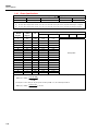
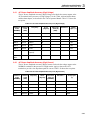
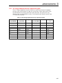
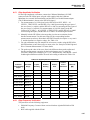
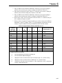
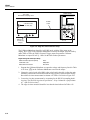
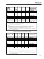
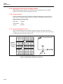
1
® 5500A Multi-Product Calibrator Service Manual PN 105798 August 1995 Rev.6, 7/06 © 1995-2006 Fluke Corporation. All rights reserved. Printed in U.S.A. All product names are trademarks of their respective companies. LIMITED WARRANTY & LIMITATION OF LIABILITY Each Fluke product is warranted to be free from defects in material and workmanship under normal use and service. The warranty period is one year and begins on the date of shipment. Parts, product repairs and services are warranted for 90 days. This warranty extends only to the original buyer or end-user customer of a Fluke authorized reseller, and does not apply to fuses, disposable batteries or to any product which, in Fluke's opinion, has been misused, altered, neglected or damaged by accident or abnormal conditions of operation or handling. Fluke warrants that software will operate substantially in accordance with its functional specifications for 90 days and that it has been properly recorded on non-defective media. Fluke does not warrant that software will be error free or operate without interruption. Fluke authorized resellers shall extend this warranty on new and unused products to end-user customers only but have no authority to extend a greater or different warranty on behalf of Fluke. Warranty support is available if product is purchased through a Fluke authorized sales outlet or Buyer has paid the applicable international price. Fluke reserves the right to invoice Buyer for importation costs of repair/replacement parts when product purchased in one country is submitted for repair in another country. Fluke's warranty obligation is limited, at Fluke's option, to refund of the purchase price, free of charge repair, or replacement of a defective product which is returned to a Fluke authorized service center within the warranty period. To obtain warranty service, contact your nearest Fluke authorized service center or send the product, with a description of the difficulty, postage and insurance prepaid (FOB Destination), to the nearest Fluke authorized service center. Fluke assumes no risk for damage in transit. Following warranty repair, the product will be returned to Buyer, transportation prepaid (FOB Destination). If Fluke determines that the failure was caused by misuse, alteration, accident or abnormal condition of operation or handling, Fluke will provide an estimate of repair costs and obtain authorization before commencing the work. Following repair, the product will be returned to the Buyer transportation prepaid and the Buyer will be billed for the repair and return transportation charges (FOB Shipping Point). THIS WARRANTY IS BUYER'S SOLE AND EXCLUSIVE REMEDY AND IS IN LIEU OF ALL OTHER WARRANTIES, EXPRESS OR IMPLIED, INCLUDING BUT NOT LIMITED TO ANY IMPLIED WARRANTY OF MERCHANTABILITY OR FITNESS FOR A PARTICULAR PURPOSE. FLUKE SHALL NOT BE LIABLE FOR ANY SPECIAL, INDIRECT, INCIDENTAL OR CONSEQUENTIAL DAMAGES OR LOSSES, INCLUDING LOSS OF DATA, WHETHER ARISING FROM BREACH OF WARRANTY OR BASED ON CONTRACT, TORT, RELIANCE OR ANY OTHER THEORY. Since some countries or states do not allow limitation of the term of an implied warranty, or exclusion or limitation of incidental or consequential damages, the limitations and exclusions of this warranty may not apply to every buyer. If any provision of this Warranty is held invalid or unenforceable by a court of competent jurisdiction, such holding will not affect the validity or enforceability of any other provision. Fluke Corporation P.O. Box 9090 Everett, WA 98206-9090 U.S.A. 5/94 Fluke Europe B.V. P.O. Box 1186 5602 BD Eindhoven The Netherlands W CAUTION This is an IEC safety Class 1 product. Before using, the ground wire in the line cord or rear panel binding post must be connected to an earth ground for safety. Interference Information This equipment generates and uses radio frequency energy and if not installed and used in strict accordance with the manufacturer’s instructions, may cause interference to radio and television reception. It has been type tested and found to comply with the limits for a Class B computing device in accordance with the specifications of Part 15 of FCC Rules, which are designed to provide reasonable protection against such interference in a residential installation. Operation is subject to the following two conditions: • This device may not cause harmful interference. • This device must accept any interference received, including interference that may cause undesired operation. There is no guarantee that interference will not occur in a particular installation. If this equipment does cause interference to radio or television reception, which can be determined by turning the equipment off and on, the user is encouraged to try to correct the interference by one of more of the following measures: • Reorient the receiving antenna • Relocate the equipment with respect to the receiver • Move the equipment away from the receiver • Plug the equipment into a different outlet so that the computer and receiver are on different branch circuits If necessary, the user should consult the dealer or an experienced radio/television technician for additional suggestions. The user may find the following booklet prepared by the Federal Communications Commission helpful: How to Identify and Resolve Radio-TV Interference Problems. This booklet is available from the U.S. Government Printing Office, Washington, D.C. 20402. Stock No. 004-000-00345-4. Declaration of the Manufacturer or Importer We hereby certify that the Fluke Model 5500A is in compliance with BMPT Vfg 243/1991 and is RFI suppressed. The normal operation of some equipment (e.g. signal generators) may be subject to specific restrictions. Please observe the notices in the users manual. The marketing and sales of the equipment was reported to the Central Office for Telecommunication Permits (BZT). The right to retest this equipment to verify compliance with the regulation was given to the BZT. Bescheinigung des Herstellers/Importeurs Hiermit wird bescheinigt, daβ die Fluke Model 5500A in Übereinstimmung mit den Bestimmungen der BMPT-AmtsblVfg 243/1991 funk-entstört sind. Der vorschriftsmäßige Betrieb mancher Geräte (z.B. Meßsender) kann allerdings gewissen Einschränkungen unterliegen. Beachten Sie deshalb die Hinweise in der Bedienungsanleitung. Dem Bundesamt für Zulassungen in der Telecommunikation wurde das Inverkehrbringen dieses Gerätes angezeigt und die Berechtigung zur Überprüfung der Serie auf Einhaltung der Bestimmungen eingeräumt. Fluke Corporation SAFETY TERMS IN THIS MANUAL This instrument has been designed and tested in accordance with IEC publication 1010-1 (1992-1), Safety Requirements for Electrical Measuring, Control and Laboratory Equipment, and ANSI/ISA-582.01-1994, and CAN/CSA-C22.2 No. 1010.1-92. This User Manual contains information, warning, and cautions that must be followed to ensure safe operation and to maintain the instrument in a safe condition. Use of this equipment in a manner not specified herein may impair the protection provided by the equipment. This instrument is designed for IEC 1010-1 Installation Category II use. It is not designed for connection to circuits rated over 4800 VA. WARNING statements identify conditions or practices that could result in personal injury or loss of life. CAUTION statements identify conditions or practices that could result in damage to equipment. SYMBOLS MARKED ON EQUIPMENT WARNING Risk of electric shock. Refer to the manual (see the Index for references). GROUND Ground terminal to chassis (earth). Attention Refer to the manual (see the Index for references). This symbol indicates that information about usage of a feature is contained in the manual. This symbol appears on the rear panel ground post and by the fuse compartment. AC POWER SOURCE The instrument is intended to operate from an ac power source that will not apply more than 264V ac rms between the supply conductors or between either supply conductor and ground. A protective ground connection by way of the grounding conductor in the power cord is required for safe operation. USE THE PROPER FUSE To avoid fire hazard, for fuse replacement use only the specified unit: 110 or 120 V operation, 2.5 ampere/250 volt time delay; 220 or 240 V operation, 1.25 ampere/250 volt time delay. GROUNDING THE INSTRUMENT The instrument utilizes controlled overvoltage techniques that require the instrument to be grounded whenever normal mode or common mode ac voltages or transient voltages may occur. The enclosure must be grounded through the grounding conductor of the power cord, or through the rear panel ground binding post. USE THE PROPER POWER CORD Use only the power cord and connector appropriate for the voltage and plug configuration in your country. Use only a power cord that is in good condition. Refer power cord and connector changes to qualified service personnel. DO NOT OPERATE IN EXPLOSIVE ATMOSPHERES To avoid explosion, do not operate the instrument in an atmosphere of explosive gas. DO NOT REMOVE COVER DURING OPERATION To avoid personal injury or death, do not remove the instrument cover without first removing the power source connected to the rear panel. Do not operate the instrument without the cover properly installed. Normal calibration is accomplished with the cover closed. Access procedures and the warnings for such procedures are contained both in this manual and in the Service Manual. Service procedures are for qualified service personnel only. DO NOT ATTEMPT TO OPERATE IF PROTECTION MAY BE IMPAIRED If the instrument appears damaged or operates abnormally, protection may be impaired. Do not attempt to operate the instrument under these conditions. Refer all questions of proper instrument operation to qualified service personnel. Table of Contents Chapter 1 Title Introduction and Specifications......................................................... 1-1 1-1. 1-2. 1-3. 1-4. 1-5. 1-6. 1-7. 1-8. 1-9. 1-10. 1-11. 1-12. 1-13. 1-14. 1-15. 1-16. 1-17. 1-18. 1-19. 1-20. 1-21. 1-22. 1-23. 1-24. 1-25. 1-26. 1-27. 1-28. 1-29. 2 Page Introduction........................................................................................... Service Information .............................................................................. Specifications........................................................................................ General Specifications...................................................................... DC Voltage Specifications ............................................................... DC Current Specifications................................................................ Resistance Specifications ................................................................. AC Voltage (Sine Wave) Specifications .......................................... AC Current (Sine Wave) Specifications........................................... Capacitance Specifications ............................................................... Temperature Calibration (Thermocouple) Specifications ................ Temperature Calibration (RTD) Specifications................................ DC Power Specification Summary................................................... AC Power (45 Hz to 65 Hz) Specification Summary, PF=1 ............ Power and Dual Output Limit Specifications................................... Phase Specifications ......................................................................... Calculating Power Uncertainty......................................................... Additional Specifications...................................................................... Frequency Specifications.................................................................. Harmonics (2nd to 50th) Specifications.............................................. AC Voltage (Sine Wave) Extended Bandwidth Specifications........ AC Voltage (Non-Sine Wave) Specifications .................................. AC Voltage, DC Offset Specifications............................................. AC Voltage, Square Wave Characteristics....................................... AC Voltage, Triangle Wave Characteristics (typical)...................... AC Current (Sine Wave) Extended Bandwidth Specifications ........ AC Current (Non-Sinewave) Specifications .................................... AC Current, Square Wave Characteristics (typical)......................... AC Current, Triangle Wave Characteristics (typical) ...................... 1-3 1-4 1-4 1-6 1-7 1-8 1-9 1-10 1-13 1-15 1-16 1-17 1-18 1-18 1-19 1-20 1-21 1-22 1-22 1-22 1-23 1-24 1-25 1-25 1-25 1-25 1-26 1-26 1-26 Theory of Operation ............................................................................ 2-1 2-1. 2-2. Introduction........................................................................................... 2-3 Encoder Assembly (A2)........................................................................ 2-4 i 5500A Service Manual 2-3. 2-4. 2-5. 2-6. 2-7. 2-8. 2-9. 2-10. 3 Synthesized Impedance Assembly (A5) ............................................... DDS Assembly (A6)............................................................................. Current Assembly (A7)......................................................................... Voltage Assembly (A8) ........................................................................ Main CPU Assembly (A9).................................................................... Power Supplies ..................................................................................... Outguard Supplies ............................................................................ Inguard Supplies............................................................................... 2-4 2-5 2-6 2-7 2-8 2-8 2-8 2-8 Calibration and Verification................................................................ 3-1 3-1. 3-2. 3-3. 3-4. 3-5. 3-6. 3-7. 3-8. 3-9. 3-10. 3-11. 3-12. 3-13. 3-14. 3-15. 3-16. 3-17. 3-18. 3-19. 3-20. 3-21. 3-22. 3-23. 3-24. 3-25. 3-26. 3-27. 3-28. 3-29. 3-30. 3-31. 3-32. 3-33. 3-34. 3-35. 3-36. 3-37. 3-38. 3-39. 3-40. 3-41. 3-42. 3-43. 3-44. Introduction........................................................................................... Calibration ............................................................................................ Equipment Required for Calibration and Verification ..................... Starting Calibration .......................................................................... How the Calibration Procedure Works............................................. DC Volts........................................................................................... AC Volts........................................................................................... Thermocouple Measuring................................................................. DC Current ....................................................................................... AC Current ....................................................................................... AUX DC Volts ................................................................................. AUX AC Volts ................................................................................. Resistance ......................................................................................... Capacitance....................................................................................... Capacitance, Four-Wire Comp ......................................................... Frequency ......................................................................................... NORMAL Volts and AUX Volts Phase........................................... Volts and AUX Current Phase ......................................................... Remote Commands for 5500A Calibration ...................................... Generating a Calibration Report ........................................................... Calibration Shifts Report, Printout Format....................................... Calibration Shifts Report, Spreadsheet Format ................................ Calibration Constant Report, Printout Format.................................. Calibration Constants Report, Spreadsheet Format.......................... Performance Verification Tests ............................................................ Zeroing the Calibrator ...................................................................... DC Voltage Amplitude Accuracy (NORMAL)................................ DC Voltage Amplitude Accuracy (AUX) ........................................ DC Current Amplitude Accuracy ..................................................... Resistance Accuracy......................................................................... Resistance DC Offset Measurement................................................. AC Voltage Amplitude Accuracy (NORMAL)................................ AC Voltage Amplitude Accuracy (AUX) ........................................ AC Current Amplitude Accuracy ..................................................... Capacitance Accuracy ...................................................................... Thermocouple Measurement Accuracy............................................ Thermocouple Sourcing Accuracy ................................................... Thermocouple Measuring Accuracy ................................................ DC Power Amplitude Accuracy (NORMAL) .................................. DC Power Amplitude Accuracy (AUX)........................................... AC Power Amplitude Accuracy (High Voltage).............................. AC Power Amplitude Accuracy (High Current) .............................. AC Power Amplitude Accuracy (High Power) ................................ Phase and Frequency Accuracy........................................................ ii 3-3 3-3 3-3 3-4 3-4 3-5 3-5 3-6 3-7 3-8 3-8 3-9 3-9 3-12 3-14 3-14 3-15 3-15 3-16 3-18 3-18 3-19 3-19 3-20 3-20 3-20 3-21 3-21 3-22 3-23 3-24 3-25 3-27 3-28 3-29 3-31 3-31 3-31 3-32 3-32 3-33 3-33 3-34 3-34 Contents (continued) 3-45. 3-46. 3-47. 3-48. 3-49. 3-50. 4 3-36 3-37 3-38 3-39 3-39 3-40 Maintenance......................................................................................... 4-1 4-1. 4-2. 4-3. 4-4. 4-5. 4-6. 4-7. 4-8. 4-9. 4-10. 4-11. 4-12. 4-13. 4-14. 4-15. 5 AC Voltage Amplitude Accuracy, Squarewave (NORMAL) .......... AC Voltage Amplitude Accuracy, Squarewave (AUX)................... AC Voltage Harmonic Amplitude Accuracy (NORMAL)............... AC Voltage Harmonic Amplitude Accuracy (AUX) ....................... DC Voltage Offset Accuracy............................................................ AC Voltage Accuracy with a DC Offset .......................................... Introduction........................................................................................... Access Procedures ................................................................................ Removing Analog Modules.............................................................. Removing the Main CPU (A9)......................................................... Removing Rear Panel Assemblies.................................................... Removing the Filter PCA (A12)....................................................... Removing the Encoder (A2) and Display PCAs .............................. Removing the Keyboard and Accessing the Output Block .............. Diagnostic Testing ................................................................................ Running Diagnostics ........................................................................ Sequence of Diagnostics Tests..................................................... Diagnostics Error Messages ......................................................... Testing the Front Panel..................................................................... Internal Fuse Replacement.................................................................... Complete List of Error Messages ......................................................... 4-3 4-3 4-3 4-3 4-4 4-4 4-4 4-4 4-7 4-7 4-7 4-7 4-13 4-14 4-14 List of Replaceable Parts.................................................................... 5-1 5-1. 5-2. 5-3. 5-4. Introduction........................................................................................... How to Obtain Parts.............................................................................. How to Contact Fluke ........................................................................... Parts Lists.............................................................................................. 5-3 5-3 5-3 5-4 6 Oscilloscope Calibration Options...................................................... 6-1 6 SC600 Option ....................................................................................... 6-3 6-1. 6-2. 6-3. 6-4. 6-5. 6-6. 6-7. 6-8. 6-9. 6-10. 6-11. 6-12. 6-13. 6-14. 6-15. 6-16. 6-17. 6-18. 6-19. 6-20. Introduction........................................................................................... Maintenance.......................................................................................... SC600 Specifications............................................................................ Volt Specifications ........................................................................... Edge Specifications .......................................................................... Leveled Sine Wave Specifications ................................................... Time Marker Specifications ............................................................. Wave Generator Specifications ........................................................ Pulse Generator Specifications......................................................... Trigger Signal Specifications (Pulse Function)................................ Trigger Signal Specifications (Time Marker Function) ................... Trigger Signal Specifications (Edge Function) ................................ Trigger Signal Specifications (Square Wave Voltage Function) ..... Trigger Signal Specifications ........................................................... Oscilloscope Input Resistance Measurement Specifications............ Oscilloscope Input Capacitance Measurement Specifications ......... Overload Measurement Specifications ............................................. Theory of Operation ............................................................................. Voltage Mode ................................................................................... Edge Mode ....................................................................................... iii 6-5 6-5 6-6 6-6 6-7 6-8 6-9 6-9 6-10 6-10 6-10 6-11 6-11 6-11 6-11 6-11 6-12 6-12 6-12 6-12 5500A Service Manual 6-21. 6-22. 6-23. 6-24. 6-25. 6-26. 6-27. 6-28. 6-29. 6-30. 6-31. 6-32. 6-33. 6-34. 6-35. 6-36. 6-37. 6-38. 6-39. 6-40. 6-41. 6-42. 6-43. 6-44. 6-45. 6-46. 6-47. 6-48. 6-49. 6-50. 6-51. 6-52. 6-53. 6-54. 6-55. 6-56. 6-57. 6-58. 6-59. 6-60. 6-61. 6-62. 6-63. 6-64. 6-65. 6-66. 6-67. 6-68. 6-69. 6-70. 6-71. 6-72. 6-73. 6-74. Leveled Sine Wave Mode ................................................................ Time Marker Mode........................................................................... Wave Generator Mode ..................................................................... Input Impedance Mode (Resistance) ................................................ Input Impedance Mode (Capacitance).............................................. Overload Mode................................................................................. Equipment Required for Calibration and Verification.......................... SC600 Calibration Setup ...................................................................... Calibration and Verification of Square Wave Voltage Functions ........ Overview of HP3458A Operation .................................................... Setup for SC600 Voltage Square Wave Measurements ................... Setup for SC600 Edge and Wave Gen Square Wave Measurements................................................................................... DC Voltage Calibration.................................................................... AC Voltage Calibration.................................................................... Wave Generator Calibration............................................................. Edge Amplitude Calibration............................................................. Leveled Sine Wave Amplitude Calibration...................................... Leveled Sine Wave Flatness Calibration.......................................... Low Frequency Calibration.......................................................... High Frequency Calibration......................................................... Pulse Width Calibration ................................................................... MeasZ Calibration ............................................................................ Verification ........................................................................................... DC Voltage Verification................................................................... Verification at 1 MΩ.................................................................... Verification at 50 Ω ..................................................................... AC Voltage Amplitude Verification................................................. Verification at 1 MΩ.................................................................... Verification at 50 Ω ..................................................................... AC Voltage Frequency Verification................................................. Edge Amplitude Verification ........................................................... Edge Frequency Verification............................................................ Edge Duty Cycle Verification .......................................................... Edge Rise Time Verification ............................................................ Edge Abberation Verification........................................................... Tunnel Diode Pulser Drive Amplitude Verification......................... Leveled Sine Wave Amplitude Verification .................................... Leveled Sine Wave Frequency Verification..................................... Leveled Sine Wave Harmonics Verification .................................... Leveled Sine Wave Flatness Verification ........................................ Equipment Setup for Low Frequency Flatness ............................ Equipment Setup for High Frequency Flatness............................ Low Frequency Verification ........................................................ High Frequency Verification........................................................ Time Marker Verification................................................................. Wave Generator Verification............................................................ Verification at 1 MΩ.................................................................... Verification at 50 Ω ..................................................................... Pulse Width Verification .................................................................. Pulse Period Verification.................................................................. MeasZ Resistance Verification......................................................... MeasZ Capacitance Verification ...................................................... Overload Function Verification........................................................ SC600 Hardware Adjustments.............................................................. iv 6-12 6-13 6-13 6-13 6-13 6-13 6-15 6-17 6-18 6-18 6-18 6-20 6-21 6-21 6-22 6-22 6-23 6-24 6-24 6-25 6-25 6-26 6-28 6-29 6-29 6-29 6-31 6-31 6-33 6-34 6-35 6-35 6-36 6-36 6-38 6-39 6-40 6-41 6-42 6-44 6-44 6-44 6-46 6-46 6-51 6-52 6-52 6-53 6-56 6-57 6-57 6-58 6-59 6-60 Contents (continued) 6-75. 6-76. 6-77. 6-78. 6-79. 6-80. 6-81. 6-82. 6 Equipment Required......................................................................... Adjusting the Leveled Sine Wave Function ..................................... Equipment Setup .......................................................................... Adjusting the Leveled Sine Wave VCO Balance......................... Adjusting the Leveled Sine Wave Harmonics ............................. Adjusting the Aberrations for the Edge Function............................. Equipment Setup .......................................................................... Adjusting the Edge Aberrations ................................................... 6-60 6-60 6-61 6-61 6-62 6-62 6-63 6-63 SC300 Option ....................................................................................... 6-65 6-83. 6-84. 6-85. 6-86. 6-87. 6-88. 6-89. 6-90. 6-91. 6-92. 6-93. 6-94. 6-95. 6-96. 6-97. 6-98. 6-99. 6-100. 6-101. 6-102. 6-103. 6-104. 6-105. 6-106. 6-107. 6-108. 6-109. 6-110. 6-111. 6-112. 6-113. 6-114. 6-115. 6-116. 6-117. 6-118. 6-119. 6-120. 6-121. 6-122. 6-123. 6-124. 6-125. 6-126. Introduction........................................................................................... Maintenance.......................................................................................... SC300 Specifications............................................................................ Voltage Function Specifications....................................................... Edge Function Specifications ........................................................... Leveled Sine Wave Function Specifications .................................... Time Marker Function Specifications .............................................. Wave Generator Specifications ........................................................ Trigger Signal Specifications for the Time Marker Function .......... Trigger Signal Specifications for the Edge Function ....................... Theory of Operation ............................................................................. Voltage Mode ................................................................................... Edge Mode ....................................................................................... Leveled Sine Wave Mode ................................................................ Time Marker Mode........................................................................... Wave Generator Mode ..................................................................... Equipment Required for Calibration and Verification.......................... SC300 Calibration Setup ...................................................................... Calibration and Verification of Square Wave Functions ...................... Overview of HP3458A Operation .................................................... Setup for Square Wave Measurements............................................. DC Voltage Calibration.................................................................... AC Square Wave Voltage Calibration.............................................. Edge Amplitude Calibration............................................................. Leveled Sine Wave Amplitude Calibration...................................... Leveled Sine Wave Flatness Calibration.......................................... Low Frequency Calibration.......................................................... High Frequency Calibration......................................................... Verification ........................................................................................... DC Voltage Verification................................................................... Verification at 1 MΩ.................................................................... Verification at 50 Ω ..................................................................... AC Voltage Amplitude Verification................................................. Verification at 1 MΩ.................................................................... Verification at 50 Ω ..................................................................... AC Voltage Frequency Verification................................................. Edge Amplitude Verification ........................................................... Edge Frequency Verification............................................................ Edge Duty Cycle Verification .......................................................... Edge Rise Time Verification ............................................................ Edge Abberation Verification........................................................... Leveled Sine Wave Reference Verification ..................................... Leveled Sine Wave Frequency Verification..................................... Leveled Sine Wave Harmonics Verification .................................... v 6-67 6-67 6-68 6-68 6-69 6-70 6-71 6-71 6-72 6-72 6-72 6-72 6-72 6-72 6-72 6-73 6-75 6-77 6-78 6-78 6-78 6-79 6-80 6-81 6-81 6-82 6-83 6-83 6-84 6-84 6-84 6-84 6-87 6-87 6-89 6-90 6-91 6-92 6-93 6-93 6-95 6-96 6-97 6-98 5500A Service Manual 6-127. Leveled Sine Wave Flatness Verification ........................................ 6-128. Equipment Setup for Low Frequency Flatness ............................ 6-129. Equipment Setup for High Frequency Flatness............................ 6-130. Low Frequency Verification ........................................................ 6-131. High Frequency Verification........................................................ 6-132. Time Marker Verification................................................................. 6-133. Wave Generator Verification............................................................ 6-134. Verification at 1 MΩ.................................................................... 6-135. Verification at 50 Ω ..................................................................... 6-136. SC300 Hardware Adjustments.............................................................. 6-137. Equipment Required......................................................................... 6-138. Adjusting the Leveled Sine Wave Function ..................................... 6-139. Equipment Setup .......................................................................... 6-140. Adjusting the Leveled Sine Wave Harmonics ............................. 6-141. Adjusting the Aberrations for the Edge Function............................. 6-142. Equipment Setup .......................................................................... 6-143. Adjusting the Edge Aberrations ................................................... 6-144. SC300 Hardware Adjustments for the A4 Board.................................. 6-145. Equipment Required......................................................................... 6-146. Adjusting the Leveled Sine Wave Function ..................................... 6-147. Equipment Setup .......................................................................... 6-148. Adjusting the Leveled Sine Wave VCO Balance......................... 6-149. Adjusting the Leveled Sine Wave Harmonics ............................. 6-150. Adjusting the Aberrations for the Edge Function............................. 6-151. Equipment Setup .......................................................................... 6-152. Adjusting the Edge Aberrations for Board 5500A-4004-1 .......... 6-153. Adjusting the Edge Aberrations for Board 5500A-4004 ............. 6-154. Adjusting the Rise Time for the Edge Function ............................... 6-155. Equipment Setup .......................................................................... 6-156. Adjusting the Edge Rise Time ..................................................... Index vi 6-100 6-100 6-100 6-102 6-102 6-107 6-108 6-109 6-109 6-111 6-112 6-112 6-112 6-112 6-113 6-113 6-113 6-115 6-115 6-115 6-115 6-115 6-116 6-117 6-117 6-118 6-120 6-122 6-122 6-122 List of Tables Table 3-1. 3-2. 3-3. 3-4. 3-5. 3-6. 3-7. 3-8. 3-9. 3-10. 3-11. 3-12. 3-13. 3-14. 3-15. 3-16. 3-17. 3-18. 3-19. 3-20. 3-21. 3-22. 3-23. 3-24. 3-25. 3-26. 3-27. 3-28. 3-29. 3-30. 3-31. 3-32. 3-33. 3-34. 3-35. 3-36. Title Required Equipment for Calibration and Verification ........................................... DC Volts Calibration Steps .................................................................................... AC Volts Calibration Steps .................................................................................... DC Current Calibration Steps ................................................................................ AC Current Calibration Steps ................................................................................ AUX DCVolts Calibration Steps ........................................................................... AUX ACVolts Calibration Steps ........................................................................... Resistance Calibration Steps .................................................................................. Capacitance Calibration Steps................................................................................ Normal Volts and AUX Volts Phase Calibration Steps ......................................... Volts and Current Phase Calibration Steps ............................................................ Jumping to a Specific Calibration Step .................................................................. DC Voltage Performance Test ............................................................................... AC Voltage Performance Test ............................................................................... DC Current Amplitude Accuracy Test................................................................... Resistance Accuracy Test....................................................................................... Resistance DC Offset Measurement Test............................................................... AC Voltage Amplitude Accuracy Test (NORMAL).............................................. AC Voltage Amplitude Accuracy Test (AUX) ...................................................... AC Current Amplitude Accuracy Test................................................................... Capacitance Accuracy Test .................................................................................... Thermocouple Measurement Accuracy Test.......................................................... Thermocouple Sourcing Accuracy Test ................................................................. Thermocouple Measuring Accuracy Test .............................................................. DC Power Amplitude Accuracy Test (NORMAL) ................................................ DC Power Amplitude Accuracy Test (AUX)......................................................... AC Power Amplitude Accuracy Test (High Voltage)............................................ AC Power Amplitude Accuracy Test (High Current) ............................................ AC Power Amplitude Accuracy Test (High Power) .............................................. Phase Accuracy Test .............................................................................................. Frequency Accuracy Test....................................................................................... AC Voltage Amplitude Accuracy, Squarewave (NORMAL) ................................ AC Voltage Amplitude Accuracy, Squarewave (AUX)......................................... AC Voltage Harmonic Amplitude Accuracy (NORMAL) .................................... AC Voltage Harmonic Amplitude Accuracy (AUX) ............................................. DC Voltage Offset Accuracy Test.......................................................................... vii Page 3-4 3-5 3-5 3-7 3-8 3-8 3-9 3-10 3-13 3-15 3-16 3-17 3-21 3-21 3-22 3-23 3-24 3-25 3-27 3-28 3-30 3-31 3-31 3-32 3-32 3-32 3-33 3-33 3-34 3-34 3-35 3-36 3-37 3-38 3-39 3-39 5500A Service Manual 3-37. 4-1. 4-2. 5-1. 5-2. 5-3. 6-1. 6-2. 6-3. 6-4. 6-5. 6-6. 6-7. 6-8. 6-9. 6-10. 6-11. 6-12. 6-13. 6-14. 6-15. 6-16. 6-17. 6-18. 6-19. 6-20. 6-21. 6-22. 6-23. 6-24. 6-25. 6-26. 6-27. 6-28. 6-29. 6-30. 6-31. 6-32. 6-33. 6-34. 6-35. 6-36. 6-37. 6-38. 6-39. 6-40. 6-41. 6-42. 6-43. 6-44. 6-45. 6-46. 6-47. 6-48. 6-49. AC Voltage Accuracy with a DC Offset ................................................................ Internal Fuse Locations .......................................................................................... Error Message Format............................................................................................ Chassis Assembly................................................................................................... Front Panel Assembly ............................................................................................ Rear Panel Assembly ............................................................................................. Volt Specifications ................................................................................................. Edge Specifications ................................................................................................ Leveled Sine Wave Specifications ......................................................................... Time Marker Specifications ................................................................................... Wave Generator Specifications .............................................................................. Pulse Generator Specifications............................................................................... Trigger Signal Specifications (Pulse Function) ..................................................... Trigger Signal Specifications (Time Marker Function) ......................................... Trigger Signal Specifications (Edge Function) ...................................................... Trigger Signal Specifications (Square Wave Voltage Function) ........................... TV Trigger Signal Specifications........................................................................... Oscilloscope Input Resistance Measurement Specifications ................................. Oscilloscope Input Capacitance Measurement Specifications ............................... Overload Measurement Specifications................................................................... SC600 Calibration and Verification Equipment .................................................... Voltage HP3458A Settings .................................................................................... Edge and Wave Generator HP3458A Settings....................................................... Verification Methods for SC600 Functions ........................................................... DC Voltage Verification at 1 MΩ.......................................................................... DC Voltage Verification at 50Ω ............................................................................ AC Voltage Verification at 1 MΩ.......................................................................... AC Voltage Verification at 50Ω ............................................................................ AC Voltage Frequency Verification ...................................................................... Edge Amplification Verification ............................................................................ Edge Frequency Verification ................................................................................. Edge Rise Time Verification.................................................................................. Edge Aberrations.................................................................................................... Tunnel Diode Pulser Amplitude Verification ........................................................ Leveled Sine Wave Amplitude Verification .......................................................... Leveled Sine Wave Frequency Verification .......................................................... Leveled Sine Wave Harmonics Verification.......................................................... Low Frequency Flatness Verification at 5.5 V....................................................... High Frequency Flatness Verification at 5.5 V...................................................... High Frequency Flatness Verification at 7.5 mV................................................... High Frequency Flatness Verification at 25 mV.................................................... High Frequency Flatness Verification at 70 mV.................................................... High Frequency Flatness Verification at 250 mV.................................................. High Frequency Flatness Verification at 800 mV.................................................. High Frequency Flatness Verification at 3.4 V...................................................... Time Marker Verification ...................................................................................... Wave Generator Verification at 1 MΩ................................................................... Wave Generator Verification at 50 Ω .................................................................... Pulse Width Verification........................................................................................ Pulse Period Verification ....................................................................................... MeasZ Resistance Verification .............................................................................. MeasZ Capacitance Verification ............................................................................ SC300 Calibration and Verification Equipment .................................................... AC Square Wave Voltage and Edge Settings for the HP3458A ............................ DC Voltage Verification at 1 MΩ.......................................................................... viii 3-40 4-14 4-14 5-5 5-8 5-10 6-6 6-7 6-8 6-9 6-9 6-10 6-10 6-10 6-11 6-11 6-11 6-11 6-11 6-12 6-15 6-19 6-20 6-28 6-30 6-31 6-32 6-33 6-34 6-35 6-36 6-38 6-39 6-39 6-40 6-41 6-43 6-46 6-47 6-48 6-48 6-49 6-49 6-50 6-50 6-51 6-54 6-55 6-56 6-57 6-58 6-59 6-75 6-78 6-85 Contents (continued) 6-50. 6-51. 6-52. 6-53. 6-54. 6-55. 6-56. 6-57. 6-58. 6-59. 6-60. 6-61. 6-62. 6-63. 6-64. 6-65. 6-66. 6-67. 6-68. 6-69. 6-70. 6-71. DC Voltage Verification at 50 Ω ........................................................................... AC Voltage Verification at 1 MΩ.......................................................................... AC Voltage Verification at 50 Ω ........................................................................... AC Voltage Frequency Verification ...................................................................... Edge Amplification Verification ............................................................................ Edge Frequency Verification ................................................................................. Edge Rise Time Verification.................................................................................. Edge Aberrations.................................................................................................... Leveled Sine Wave Amplitude Verification .......................................................... Leveled Sine Wave Frequency Verification .......................................................... Leveled Sine Wave Harmonics Verification.......................................................... Low Frequency Flatness Verification at 5.5 V....................................................... High Frequency Flatness Verification at 5.5 V...................................................... High Frequency Flatness Verification at 7.5 mV................................................... High Frequency Flatness Verification at 25 mV.................................................... High Frequency Flatness Verification at 70 mV.................................................... High Frequency Flatness Verification at 250 mV.................................................. High Frequency Flatness Verification at 800 mV.................................................. High Frequency Flatness Verification at 3.4 V...................................................... Time Marker Specifications ................................................................................... Wave Generator Verification at 1 MΩ................................................................... Wave Generator Verification at 50 Ω .................................................................... ix 6-86 6-88 6-89 6-91 6-92 6-92 6-95 6-96 6-97 6-98 6-99 6-102 6-103 6-104 6-104 6-105 6-105 6-106 6-106 6-108 6-110 6-111 5500A Service Manual x List of Figures Figure 1-1. 2-1. 2-2. 2-3. 2-4. 2-5. 3-1. 3-2. 3-3. 3-4. 3-5. 3-6. 3-7. 3-8. 4-1. 4-2. 5-1. 5-2. 5-3. 5-4. 6-1. 6-2. 6-3. 6-4. 6-5. 6-6. 6-7. 6-8. 6-9. 6-10. 6-11. 6-12. 6-13. 6-14. 6-15. Title 5500A Multi-Product Calibrator ............................................................................ 5500A Internal Layout ........................................................................................... Synthesized Resistance Function ........................................................................... Synthesized Capacitance Function......................................................................... Current Function .................................................................................................... Voltage Function.................................................................................................... Connections for Calibrating TC Measure .............................................................. Connections for Calibrating DC Current ............................................................... Connections for Calibrating Four-Wire Ohms....................................................... High End Resistance Connections with Equation.................................................. LCR Meter Connections......................................................................................... Connections for Four-Wire Compensated Capacitance ......................................... Normal Volts and AUX Volts Phase Calibration................................................... Volts and Current Phase Calibration ...................................................................... Exploded View of Rear Panel Assemblies............................................................. Exploded View of Front Panel Assemblies............................................................ Chassis Assembly................................................................................................... Front Panel Assembly ............................................................................................ Rear Panel Assembly ............................................................................................. Wiring Diagram ..................................................................................................... SC600 Block Diagram ........................................................................................... Equipment Setup for SC600 Voltage Square Wave Measurements ...................... Equipment Setup for SC600 Edge and Wave Gen Square Wave Measurements .. Connecting the Calibrator Mainframe to the 5790A AC Measurement Standard . MeasZ Function Calibration Setup ........................................................................ AC Voltage Frequency Verification Setup ............................................................ Edge Rise Time Verification Setup........................................................................ Edge Rise Time ...................................................................................................... Leveled Sine Wave Harmonics Verification Setup................................................ Connecting the Calibrator Mainframe to the 5790A AC Measurement Standard . Connecting the HP E4418A Power Meter to the HP 8482A or 8481D Power Sensor.......................................................................................................... Connecting the Calibrator Mainframe to the HP Power Meter and Power Sensor Wave Generator Verification Setup ....................................................................... Overload Function Verification Setup ................................................................... Adjusting the Leveled Sine Wave Balance ............................................................ xi Page 1-4 2-3 2-4 2-5 2-6 2-7 3-6 3-7 3-9 3-11 3-12 3-14 3-15 3-16 4-5 4-6 5-6 5-9 5-11 5-12 6-14 6-19 6-20 6-24 6-27 6-34 6-37 6-38 6-42 6-44 6-45 6-45 6-52 6-59 6-61 5500A Service Manual 6-16. 6-17. 6-18. 6-19. 6-20. 6-21. 6-22. 6-23. 6-24. 6-25. 6-26. 6-27. 6-28. 6-29. 6-30. 6-31. 6-32. 6-33. 6-34. 6-35. 6-36. 6-37. 6-38. Adjusting the Leveled Sine Wave Harmonics ....................................................... Adjusting Short-Term Edge ................................................................................... SC300 Block Diagram ........................................................................................... Equipment Setup for SC300 Square Wave Measurements .................................... Connecting the Calibrator Mainframe to the 5790A AC Measurement Standard . Frequency Verification Setup................................................................................. Edge Rise Time Verification Setup........................................................................ Edge Rise Time ...................................................................................................... Leveled Sine Wave Harmonics Verification Setup................................................ Connecting the Calibrator Mainframe to the 5790A AC Measurement Standard . Connecting the HP E4418A Power Meter to the HP 8482A or 8481D Power Sensor.......................................................................................................... Connecting the Calibrator Mainframe to the HP Power Meter and Power Sensor Wave Generator Verification Setup ....................................................................... Adjusting the Leveled Sine Wave Harmonics ....................................................... Adjusting Short-Term Edge ................................................................................... Adjusting the Leveled Sine Wave Balance ............................................................ Adjusting the Leveled Sine Wave Harmonics ....................................................... Adjusting the Wave Peak Center with R168.......................................................... Adjusting Base of Peak with R57 .......................................................................... Adjusting the Ledge with R16 ............................................................................... Adjusting the Peak Base with R57......................................................................... Adjust the Ledge Flatness with R1 ........................................................................ Adjusting the Edge Rise Time with C1.................................................................. xii 6-62 6-64 6-74 6-79 6-82 6-90 6-94 6-95 6-98 6-100 6-101 6-101 6-109 6-113 6-114 6-116 6-117 6-119 6-119 6-120 6-121 6-121 6-122 Chapter 1 Introduction and Specifications Title 1-1. 1-2. 1-3. 1-4. 1-5. 1-6. 1-7. 1-8. 1-9. 1-10. 1-11. 1-12. 1-13. 1-14. 1-15. 1-16. 1-17. 1-18. 1-19. 1-20. 1-21. 1-22. 1-23. 1-24. 1-25. 1-26. 1-27. 1-28. 1-29. Introduction........................................................................................... Service Information .............................................................................. Specifications........................................................................................ General Specifications...................................................................... DC Voltage Specifications ............................................................... DC Current Specifications................................................................ Resistance Specifications ................................................................. AC Voltage (Sine Wave) Specifications .......................................... AC Current (Sine Wave) Specifications........................................... Capacitance Specifications ............................................................... Temperature Calibration (Thermocouple) Specifications ................ Temperature Calibration (RTD) Specifications................................ DC Power Specification Summary................................................... AC Power (45 Hz to 65 Hz) Specification Summary, PF=1 ............ Power and Dual Output Limit Specifications................................... Phase Specifications ......................................................................... Calculating Power Uncertainty......................................................... Additional Specifications...................................................................... Frequency Specifications.................................................................. Harmonics (2nd to 50th) Specifications.............................................. AC Voltage (Sine Wave) Extended Bandwidth Specifications........ AC Voltage (Non-Sine Wave) Specifications .................................. AC Voltage, DC Offset Specifications............................................. AC Voltage, Square Wave Characteristics....................................... AC Voltage, Triangle Wave Characteristics (typical)...................... AC Current (Sine Wave) Extended Bandwidth Specifications ........ AC Current (Non-Sinewave) Specifications .................................... AC Current, Square Wave Characteristics (typical)......................... AC Current, Triangle Wave Characteristics (typical) ...................... Page 1-3 1-4 1-4 1-6 1-7 1-8 1-9 1-10 1-13 1-15 1-16 1-17 1-18 1-18 1-19 1-20 1-21 1-22 1-22 1-22 1-23 1-24 1-25 1-25 1-25 1-25 1-26 1-26 1-26 1-1 5500A Service Manual 1-2 Introduction and Specifications Introduction 1 1-1. Introduction The Fluke Model 5500A Multi-Product Calibrator (Figure 1-1) is a precise instrument that calibrates a wide variety of electrical measuring instruments. With the 5500A Calibrator, you can calibrate precision multimeters that measure ac or dc voltage, ac or dc current, ac or dc power, resistance, capacitance, and temperature. With the Oscilloscope Calibration option, you can use the 5500A Calibrator to calibrate analog and digital oscilloscopes. Specifications for the standard 5500A are provided at the end of this chapter. Specifications for the Oscilloscope Option are in Chapter 6. XW Warning If the 5500A Calibrator is operated in any way not specified by the 5500A Operators Manual or other documentation provided by Fluke, protection provided by the 5500A may be impaired. The 5500A Calibrator is a fully programmable precision source of the following: • DC voltage from 0 V to ±1020 V. • AC voltage from 1 mV to 1020 V, with output from 10 Hz to 500 kHz. • AC current from 0.01 µA to 11.0 A, with output from 10 Hz to 10 kHz. • DC current from 0 to ±11.0 A. • Resistance values from a short circuit to 330 MΩ. • Capacitance values from 330 pF to 1100 µF. • Simulated output for three types of Resistance Temperature Detectors (RTDs). • Simulated output for nine types of thermocouples. Features of the 5500A Calibrator include the following: • Automatic meter error calculation using a simple output adjust knob. • Keys that multiply and divide the output value by 10 to simplify work on meters with calibration points at decade multiples. • Programmable entry limits to restrict levels that may be keyed into the 5500A, to prevent calling up a level that may be harmful to equipment or personnel. • Simultaneous output of voltage and current, up to 11 kW. • Simultaneous output of two voltages. • Extended bandwidth mode outputs multiple waveforms down to 0.01 Hz, and sine waves to 2 MHz. • Variable phase signal output. • Standard IEEE-488 (GPIB) interface, complying with ANSI/IEEE Standards 488.1-1987 and 488.2-1987. • EIA Standard RS-232-C serial data interface for printing, displaying, or transferring internally stored calibration constants, and for remote control of the 5500A. • Pass-through RS-232-C serial data interface for communicating with the Unit Under Test (UUT). • Extensive automatic internal self-testing and diagnostics of analog and digital functions. 1-3 5500A Service Manual 5500A CALIBRATOR NORMAL AUX V, , RTD A, SCOPE -SENSE, AUX V 60V PK MAX STBY OPR EARTH 7 8 9 5 6 SCOPE PREV MENU BOOST HI 1000V RMS MAX 20V RMS MAX TRIG OUT LO 4 1V PK MAX 20V PK MAX 1 2 3 µ m n k dBm sec V W A Hz ¡F M F TC +/ 20V PK MAX 0 ¡C SETUP RESET NEW REF CE MEAS TC TRIG OUT MULT DIV EDIT FIELD p SHIFT ENTER x POWER om001f.eps Figure 1-1. 5500A Multi-Product Calibrator 1-2. Service Information In case of difficulty within the 1-year Warranty period, return the Calibrator to a Fluke Service Center for Warranty repair. For out of Warranty repair, contact a Fluke Service Center for a cost estimate. This service manual provides instructions for verification of performance, calibration, and maintenance. If you choose to repair a malfunction, information in this manual can help you to determine which module (printed circuit assembly) has a fault. See Chapter 5 for cautions about handling the internal components. 1-3. Specifications The following paragraphs detail specifications for the 5500A Calibrator. The specifications are valid after allowing a warm-up period of 30 minutes, or twice the time the 5500A has been turned off. For example, if the 5500A has been turned off for 5 minutes, the warm-up period is 10 minutes. All specifications apply for the temperature and time period indicated. For temperatures outside of tcal + 5 °C (tcal is the ambient temperature when the 5500A was calibrated), the temperature coefficient is less than 0.1 times the 90-day specifications per °C (limited to 0 °C to 50 °C). These specifications also assume the 5500A Calibrator is zeroed every seven days or when the ambient temperature changes more than 5 °C. (See “Zeroing the Calibrator” in Chapter 4 of the 5500A Operator Manual.) Also see additional specifications later in this chapter for information on extended specifications for ac voltage and current. The dimensional outline for the 5500A Calibrator is shown in Figure A. 1-4 Introduction and Specifications Specifications 1 43.2 cm (17 in) 5500A CALIBRATOR NORMAL SCOPE AUX V, , RTD A, -SENSE, AUX V 200V PK MAX STBY OPR EARTH 7 8 9 4 5 6 1 2 3 +/ 0 SCOPE 17.8 cm (7 in) PREV MENU BOOST HI 1000V RMS MAX 20V RMS MAX TRIG OUT LO µ dBm m n W k sec V Hz ¡F A NEW REF CE F MEAS TC TRIG OUT MULT DIV p M TC 20V PK MAX SHIFT RESET ¡C 1V PK MAX 20V PK MAX SETUP ENTER x EDIT FIELD POWER I O 47.0 cm (18.5 in) 6.4 cm (2.5 in) For Cable Access om002f.ewps Figure A. 5500A Calibrator Dimensional Outline 1-5 5500A Service Manual 1-4. General Specifications Warmup Time Settling Time Standard Interfaces Temperature Performance Twice the time since last warmed up, to a maximum of 30 minutes. Less than 5 seconds for all functions and ranges except as noted. IEEE-488 (GPIB), RS-232, 5725ª Amplifier Temperature Coefficient Temperature Coefficient for temperatures outside tcal +5 °C is 0.1X/ °C of the 90-day specification (or 1-year, as applicable) per °C. Relative Humidity [1] Altitude Safety Analog Low Isolation EMC Line Power Power Consumption Dimensions Weight (without options) Absolute Uncertainty Definition Specification Confidence Interval [1] 1-6 • Operating: 0 °C to 50 °C • Calibration (tcal): 15 °C to 35 °C • Storage: -20 °C to 70 °C • Operating: <80 % to 30 °C, <70 % to 40 °C, <40 % to 50 °C • Storage: <95 %, non-condensing • Operating: 3,050 m (10,000 ft) maximum • Non-operating: 12,200 m (40,000 ft) maximum Complies with IEC 1010-1 (1992-1); ANSI/ISA-S82.01-1994; CAN/CSA-C22.2 No. 1010.1-92 20 V Designed to comply with FCC Rules Part 15; VFG 243/1991. If used in areas with Electromagnetic fields of 1 to 3 V/m, resistance outputs have a floor adder of 0.508 Ω. Performance not specified above 3 V/m. This instrument may be susceptible to electro-static discharge (ESD) from direct contact to the binding posts. Good static aware practices should be followed when handling this and other pieces of electronic equipment. • Line Voltage (selectable): 100 V, 120 V, 220 V, 240 V • Line Frequency: 47 Hz to 63 Hz • Line Voltage Variation: ±10 % about line voltage setting 5500A Calibrator, 300 VA; 5725A Amplifier, 750 VA 5500A Calibrator: • Height: 17.8 cm (7 in), standard rack increment, plus 1.5 cm (0.6 in) for feet on bottom of unit • Width, 43.2 cm (17 in), standard rack width • Depth: 47.3 cm (18.6 in) overall 5725A Amplifier: • Height, 13.3 cm (5.25 in), standard rack increment, plus 1.5 cm (0.6 in) for feet on bottom of unit • Width, 43.2 cm (17 in), standard rack width • Depth, 63.0 cm (24.8 in) overall. 5500A Calibrator, 22 kg (49 lb); 5725A Amplifier 32 kg (70 lb) The 5500A specifications include stability, temperature coefficient, linearity, line and load regulation, and the traceability of the external standards used for calibration. You do not need to add anything to determine the total specification of the 5500A for the temperature range indicated. 99 % After long periods of storage at high humidity, a drying out period (with the power on) of at least one week may be required. Introduction and Specifications Specifications 1-5. 1 DC Voltage Specifications Range Absolute Uncertainty, tcal ± 5 °C ± (% of output + µV) 90 days Stability 24 hours, ± 1 °C ± (ppm output + µV) 1 year Resolution µV Maximum [1] Burden 0 to 329.9999 mV 0.005 3 0.006 3 5+1 0.1 50 Ω 0 to 3.299999 V 0.004 5 0.005 5 4+3 1 10 mA 0 to 32.99999 V 0.004 50 0.005 50 4 + 30 10 10 mA 30 to 329.9999 V 0.0045 500 0.0055 500 4.5 + 300 100 5 mA 100 to 1020.000 V 0.0045 1500 0.0055 1500 4.5 + 900 1000 5 mA Auxiliary Output (dual output mode only) [2] 0 to 329.999 mV 0.03 350 0.04 350 30 + 100 1 5 mA 0.33 to 3.3 V 0.03 350 0.04 350 30 + 100 10 5 mA [1] Remote sensing is not provided. Output resistance is < 5 mΩ for outputs ≥ 0.33 V. The AUX output has an output resistance of < 1 Ω. [2] Two channels of dc voltage output are provided. Noise Range Bandwidth 0.1 to 10 Hz p-p ± (ppm output + µV) Bandwidth 10 to 10 kHz rms 0 to 329.9999 mV 1 µV 4 µV 0 to 3.299999 V 10 µV 50 µV 600 µV 0 to 32.99999 V 100 µV 30 to 329.9999 V 10 ppm + 1 mV 20 mV 100 to 1020.000 V 10 ppm + 5 mV 20 mV Auxiliary Output (dual output mode only) [1] 0 to 329.999 mV 5 µV 20 µV 0.33 to 3.3 V 20 µV 200 µV [1] Two channels of dc voltage output are provided. 1-7 5500A Service Manual 1-6. DC Current Specifications Absolute Uncertainty, tcal ± 5 °C ± (% of output + µA) Range 90 days Resolution Compliance Voltage 1 year Maximum Inductive Load 0 to 3.29999 mA 0.010 0.05 0.013 0.05 0.01 µA 4.5 V 1 µH 0 to 32.9999 mA 0.008 0.25 0.01 0.25 0.1 µA 4.5 V 200 µH 0 to 329.999 mA 0.008 3.3 0.01 3.3 1 µA 4.5 to 3.0 V [1] 200 µH 200 µH 200 µH 0 to 2.19999 A 0.023 44 0.03 44 10 µA 4.5 to 3.4 V [2] 0 to 11 A 0.038 330 0.06 330 100 µA 4.3 to 2.5 V [3] 5725A Amplifier 0 to 11 A 0.03 330 0.04 330 100 4V [1] The actual voltage compliance (Vc) is a function of current output (Io), and is given by the formula: Vc = -5.05*Io+4.67. The highest compliance voltage is limited to 4.5 V. [2] The actual voltage compliance (Vc) is a function of current output (Io), and is given by the formula: Vc = -0.588*Io+4.69. The highest compliance voltage is limited to 4.5 V. [3] The actual voltage compliance (Vc) is a function of current output (Io), and is given by the formula: Vc = -0.204*Io+4.75. The highest compliance voltage is limited to 4.3 V. Noise Bandwidth 0.1 to 10 Hz p-p Bandwidth 10 to 10 kHz rms 0 to 3.29999 mA 20 nA 200 nA 0 to 32.9999 mA 200 nA 2.0 µA 0 to 329.999 mA 2000 nA 20 µA Ranges 0 to 2.19999 A 20 µA 1 mA 0 to 11 A 200 µA 10 mA 0 to 11 A ± 25 ppm of output + 200 nA 5725A Amplifier 1-8 2 mA 400 µH Introduction and Specifications Specifications 1-7. 1 Resistance Specifications Range Absolute Uncertainty, tcal ± 5 °C [2] ± (% of output + Ω) [1] 90 days 0 to 10.99 Ω 0.009 Resolution Ω 1 year Allowable [4] Current 0.008 [3] 0.012 0.008 [3] 0.001 1 to 125 mA 0.012 0.015 [3] 0.001 1 to 125 mA 11 to 32.999 Ω 0.009 0.015 [3] 33 to 109.999 Ω 0.007 0.015 [3] 0.009 0.015 [3] 0.001 1 to 70 mA 0.015 [3] 0.009 0.015 [3] 0.001 1 to 40 mA 250 µA to 18 mA 110 to 329.999 Ω 0.007 330 Ω to 1.09999 kΩ 0.007 0.06 0.009 0.06 0.01 1.1 to 3.29999 kΩ 0.007 0.06 0.009 0.06 0.01 250 µA to 5 mA 3.3 to 10.9999 kΩ 0.007 0.6 0.009 0.6 0.1 25 µA to 1.8 mA 11 to 32.9999 kΩ 0.007 0.6 0.009 0.6 0.1 25 µA to 0.5 mA 33 to 109.999 kΩ 0.008 6 0.011 6 1 2.5 µA to 0.18 mA 110 to 329.999 kΩ 0.009 6 0.012 6 1 2.5 µA to 0.05 mA 330 kΩ to 1.09999 MΩ 0.011 55 0.015 55 10 250 nA to 0.018 mA 1.1 to 3.29999 MΩ 0.011 55 0.015 55 10 250 nA to 5 µA 3.3 to 10.9999 MΩ 0.045 550 0.06 550 100 25 nA to 1.8 µA 11 to 32.9999 MΩ 0.075 550 0.1 550 100 25 nA to 0.5 µA 33 to 109.999 MΩ 0.4 5500 0.5 5500 1000 2.5 nA to 0.18 µA 110 to 330 MΩ 0.4 16500 0.5 16500 1000 2.5 nA to 0.06 µA [1] Continuously variable from 0 to 330 MΩ. [2] Applies for COMP OFF (to the 5500A Calibrator front panel NORMAL terminals) and 2-wire and 4-wire compensation. [3] The floor adder is improved to 0.006 Ω (0 to 10.99 Ω range) and 0.010 Ω (11 to 329.999 Ω) if the 5500A Calibrator is zeroed (ohms zero or instrument zero) within 8 hours and temperature is ±1 °C of zeroing ambient temperature. [4] Do not exceed the largest current for each range. For currents lower than shown, the floor adder increases by Floor(new) = Floor(old) x Imin/Iactual. For example, a 100 µA stimulus measuring 100 Ω has a floor uncertainty of 0.01 Ω x 1 mA/100 µA = 0.1 Ω. Range Maximum Voltage [1] Maximum Lead Resistance 0 to 10.99 Ω 1.37 V <3.2 Ω 11 to 32.999 Ω 4.12 V <3.2 Ω 33 to 109.999 Ω 7.7 V <3.2 Ω 110 to 329.999 Ω 13.2 V <3.2 Ω 330 Ω to 1.09999 kΩ 19.8 V <6 Ω 1.1 to 3.29999 kΩ 16.5 V <6 Ω 3.3 to 10.9999 kΩ 19.8 V <6 Ω 11 to 32.9999 kΩ 16.5 V <6 Ω <6 Ω 33 to 109.999 kΩ 19.8 V 110 to 329.999 kΩ 16.5 V 330 kΩ to 1.09999 MΩ 19.8 V 1.1 to 3.29999 MΩ 16.5 V 3.3 to 10.9999 MΩ 19.8 V 11 to 32.9999 MΩ 16.5 V 33 to 109.999 MΩ 19.8 V 110 to 330 MΩ 19.8 V [2] (n/a 110 kΩ and above) [1] This is for the largest resistance for each range. The maximum voltage for other values is Imax (highest value of Allowable Current above) multiplied by Rout. [2] Maximum lead resistance for no additional error in 2-wire COMP. 1-9 5500A Service Manual 1-8. AC Voltage (Sine Wave) Specifications Range Frequency Absolute Uncertainty, tcal ± 5 °C ± (% of output + µV) 90 days 1.0 to 32.999 mV 33 to 329.999 mV 0.33 to 3.29999 V 3.3 to 32.9999 V 33 to 329.999 V 330 to 1020 V 1-10 Resolution Max [1] Burden 1 µV 50 Ω 1 µV 50 Ω 10 µV 10 mA 100 µV 10 mA 1 mV 5 mA, except 20 mA for 45 to 65 Hz 10 mV 2 mA, except 6 mA for 45 to 65 Hz 1 year 10 to 45 Hz 0.26 20 0.35 20 45 Hz to 10 kHz 0.11 20 0.15 20 10 to 20 kHz 0.15 20 0.2 20 20 to 50 kHz 0.19 20 0.25 20 50 to 100 kHz 0.26 33 0.35 33 100 to 500 kHz 0.75 60 1 60 10 to 45 Hz 0.19 50 0.25 50 45 Hz to 10 kHz 0.04 20 0.05 20 10 to 20 kHz 0.08 20 0.1 20 20 to 50 kHz 0.12 40 0.16 40 50 to 100 kHz 0.17 170 0.24 170 100 to 500 kHz 0.53 330 0.7 330 10 to 45 Hz 0.11 250 0.15 250 45 Hz to 10 kHz 0.02 60 0.03 60 10 to 20 kHz 0.06 60 0.08 60 20 to 50 kHz 0.10 300 0.14 300 50 to 100 kHz 0.17 1700 0.24 1700 100 to 500 kHz 0.38 3300 0.5 3300 2500 10 to 45 Hz 0.11 2500 0.15 45 Hz to 10 kHz 0.03 600 0.04 600 10 to 20 kHz 0.06 2600 0.08 2600 20 to 50 kHz 0.14 5000 0.19 5000 50 to 100 kHz 0.17 17000 0.24 17000 45 Hz to 1 kHz 0.04 6.6 mV 0.05 6.6 mV 1 to 10 kHz 0.06 15 0.08 15 10 to 20 kHz 0.07 33 0.09 33 45 Hz to 1 kHz 0.04 80 mV 0.05 80 mV 1 to 5 kHz 0.15 100 0.20 100 5 to 10 kHz 0.15 500 0.20 500 Introduction and Specifications Specifications 1 AC Voltage (Sine Wave) Specifications (cont.) Range Frequency Absolute Uncertainty, tcal ± 5 °C ± (% of output + µV) 90 days Resolution 1 year Maximum [1] Burden 5725A Amplifier 100 to 1020 V 100 to 750 V 45 Hz to 1 kHz 0.04 80 mV 0.05 80 mV 50 mA 1 to 20 kHz 0.06 100 mV 0.08 100 mV 70 mA 20 to 30 kHz 0.08 100 mV 0.10 100 mV 30 to 100 kHz 0.38 500 mV 0.5 500 mV Auxiliary Output [dual output mode only] 10 to 329.999 mV 0.33 to 3.29999 V 10 mV 70 mA 70 mA [2] 10 to 20 Hz 0.15 370 0.2 370 20 to 45 Hz 0.08 370 0.1 370 45 Hz to 1 kHz 0.08 370 0.1 370 1 to 5 kHz 0.15 450 0.2 450 5 to 10 kHz 0.3 450 0.4 450 10 to 20 Hz 0.15 450 0.2 450 20 to 45 Hz 0.08 450 0.1 450 45 Hz to 1 kHz 0.07 450 0.09 450 1 to 5 kHz 0.15 1400 0.2 1400 5 to 10 kHz 0.3 1400 0.4 1400 1 µV 5 mA 10 µV 5 mA [1] Remote sensing is not provided. Output resistance is < 5 mΩ for outputs ≥ 0.33 V. The AUX output resistance is < 1 Ω. The maximum load capacitance is 500 pF, subject to the maximum burden current limits. [2] There are two channels of voltage output. The maximum frequency of the dual output is 10 kHz. 1-11 5500A Service Manual AC Voltage (Sine Wave) Specifications (cont.) Range 1.0 to 32.999 mV 33 to 329.999 mV 0.33 to 3.29999 V 3.3 to 32.9999 V 33 to 329.999 V 330 to 1000 V Frequency Maximum Distortion and Noise 10 Hz to 5 MHz Bandwidth ± (% output + µV) 10 to 45 Hz 45 Hz to 10 kHz 0.15 + 90 0.035 + 90 10 to 20 kHz 0.06 + 90 20 to 50 kHz 0.15 + 90 50 to 100 kHz 0.25 + 90 100 to 500 kHz 10 to 45 Hz 45 Hz to 10 kHz 0.3 + 90 0.15 + 90 0.035 + 90 10 to 20 kHz 0.06 + 90 20 to 50 kHz 0.15 + 90 50 to 100 kHz 0.20 + 90 100 to 500 kHz 10 to 45 Hz 45 Hz to 10 kHz 0.20 + 90 0.15 + 200 0.035 + 200 10 to 20 kHz 0.06 + 200 20 to 50 kHz 0.15 + 200 50 to 100 kHz 0.20 + 200 100 to 500 kHz 10 to 45 Hz 45 Hz to 10 kHz 0.20 + 200 0.15 + 2 mV 0.035 + 2 mV 10 to 20 kHz 0.08 + 2 mV 20 to 50 kHz 0.2 + 2 mV 50 to 100 kHz 45 Hz to 1 kHz 1 to 10 kHz 0.5 + 2 mV 0.15 + 10 mV 0.05 + 10 mV 10 to 20 kHz 0.6 + 10 mV 45 Hz to 1 kHz 1 to 10 kHz 0.15 + 30 mV 0.07 + 30 mV 5725A Amplifier 100 to 1020 V 45 Hz to 1 kHz 1 to 20 kHz 0.07 % 0.15 % 100 to 750 V 20 to 30 kHz 30 to 100 kHz 0.3 % 0.4 % Auxiliary Output (dual output mode only) 10 Hz to 100 kHz Bandwidth 10 to 329.999 mV 0.33 to 3.29999 V 1-12 10 to 20 Hz 20 to 45 Hz 0.2 + 200 0.06 + 200 45 Hz to 1 kHz 0.08 + 200 1 to 5 kHz 0.3 + 200 5 to 10 kHz 10 to 20 Hz 20 to 45 Hz 0.6 + 200 0.2 + 200 0.06 + 200 45 Hz to 1 kHz 1 to 5 kHz 0.08 + 200 0.3 + 200 5 to 10 kHz 0.6 + 200 Introduction and Specifications Specifications 1-9. 1 AC Current (Sine Wave) Specifications Range Frequency Absolute Uncertainty, tcal ± 5 °C ± (% of output + µA) 90 days 0.029 to 0.32999 mA 0.33 to 3.2999 mA 3.3 to 32.999 mA 33 to 329.99 mA Resolution Compliance Voltage Max Inductive Load 0.01 µA 3.0 V rms 1 µH 0.01 µA 3.0 V rms 1 µH 1 year 10 to 20 Hz 20 to 45 Hz 0.19 0.09 0.15 0.15 0.25 0.125 0.15 0.15 45 Hz to 1 kHz 0.09 0.25 0.125 0.25 1 to 5 kHz 0.30 0.15 0.4 0.15 5 to 10 kHz 10 to 20 Hz 20 to 45 Hz 0.94 0.15 0.08 0.15 0.3 0.3 1.25 0.2 0.1 0.15 0.3 0.3 45 Hz to 1 kHz 0.08 0.3 0.1 0.3 1 to 5 kHz 0.15 0.3 0.2 0.3 5 to 10 kHz 0.45 0.3 0.6 0.3 10 to 20 Hz 0.15 3 0.2 3 20 to 45 Hz 0.08 3 0.1 3 45 Hz to 1 kHz 0.07 3 0.09 3 1 to 5 kHz 0.15 3 0.2 3 5 to 10 kHz 0.45 3 0.6 3 10 to 20 Hz 20 to 45 Hz 0.15 0.08 30 30 0.2 0.1 30 30 45 Hz to 1 kHz 0.07 30 0.09 30 1 to 5 kHz 0.15 30 0.2 30 5 to 10 kHz 0.45 30 0.6 30 10 to 45 Hz 0.15 300 0.2 300 45 Hz to 1 kHz 0.08 300 0.1 300 0.1 µA 1 µA 10 µA 0.33 to 2.19999 A 1 to 5 kHz 0.7 300 0.75 300 45 to 65 Hz 0.05 2000 0.06 2000 65 to 500 Hz 0.08 2000 0.10 2000 100 µA 2.2 to 11 A 500 Hz to 1 kHz 0.25 2000 0.33 2000 3.0 V rms 3.0 to [1] 2.0 V rms 3.0 to [2] 2.0 V rms 2.8 to [3] 1.25 V rms 200 µH, 10 to 500 Hz 1 µH, 500 Hz to 10 kHz 200 µH, 10 to 500 Hz 5 µH, 500 Hz to 10 kHz 200 µH, 45 to 500 Hz 5 µH, 500 Hz to 5 kHz 200 µH, 45 to 65 Hz 1 µH, 65 Hz to 1 kHz 1-13 5500A Service Manual AC Current (Sine Wave) Specifications (cont.) Range Frequency Absolute Uncertainty, tcal ± 5 °C ± (% of output + µA) 90 days Resolution Compliance Voltage Max Inductive Load 100 3 400 µH 1 year 5725A Amplifier 1.5 to 11 A 45 Hz to 1 kHz 1 to 5 kHz 0.08 0.19 100 5000 0.1 0.25 100 5000 5 to 10 kHz 0.75 10000 1 10000 [1] The actual voltage compliance (Vc) is a function of current output (Io), and is given by the formula: Vc = -3.37*Io+3.11. The highest compliance voltage is limited to 3.0 V. [2] The actual voltage compliance (Vc) is a function of current output (Io), and is given by the formula: Vc = -0.535*Io+3.18. The highest compliance voltage is limited to 3.0 V. [3] The actual voltage compliance (Vc) is a function of current output (Io), and is given by the formula: Vc = -0.176*Io+3.19. The highest compliance voltage is limited to 2.8 V. Range 0.02 to 0.32999 mA 0.33 to 3.2999 mA 3.3 to 32.999 mA 33 to 329.99 mA 0.33 to 2.19999 A 2.2 to 11 A Frequency Maximum Distortion and Noise 10 Hz to 100 kHz Bandwidth ± (% output + µA) 10 to 20 Hz 0.15 20 to 45 Hz 0.1 1.0 1.0 45 Hz to 1 kHz 0.05 1.0 1 to 5 kHz 0.5 1.0 5 to 10 kHz 1.0 1.0 10 to 20 Hz 0.15 1.5 20 to 45 Hz 0.06 1.5 45 Hz to 1 kHz 0.02 1.5 1 to 5 kHz 0.5 1.5 5 to 10 kHz 1.2 1.5 10 to 20 Hz 0.15 5 20 to 45 Hz 0.05 5 45 Hz to 1 kHz 0.07 5 5 1 to 5 kHz 0.3 5 to 10 kHz 0.7 5 10 to 20 Hz 0.15 50 20 to 45 Hz 0.05 50 45 Hz to 1 kHz 0.07 50 50 1 to 5 kHz 0.2 5 to 10 kHz 0.4 50 10 to 45 Hz 0.2 500 45 Hz to 1 kHz 0.1 500 1 to 5 kHz 1.4 500 45 to 65 Hz 0.2 3 mA 65 to 500 Hz 0.1 3 mA 500 Hz to 1 kHz 0.4 3 mA 45 Hz to 1 kHz 0.05 1 mA 1 to 5 kHz 0.12 1 mA 5 to 10 kHz 0.5 1 mA 5725A Amplifier 1.5 to 11 A 1-14 Introduction and Specifications Specifications 1 1-10. Capacitance Specifications Range Absolute Uncertainty, tcal ± 5 °C ± (% of output + nF) 90 days Frequency Resolution 1 year Allowed Typical for <1 % Error 0.33 to 0.4999 nF 0.38 0.01 0.5 0.01 0.1 pF 50 to 1000 Hz 10 kHz 0.5 to 1.0999 nF 0.38 0.01 0.5 0.01 0.1 pF 50 to 1000 Hz 10 kHz 1.1 to 3.2999 nF 0.38 0.01 0.5 0.01 0.1 pF 50 to 1000 Hz 10 kHz 3.3 to 10.999 nF 0.38 0.01 0.5 0.01 1 pF 50 to 1000 Hz 10 kHz 11 to 32.999 nF 0.19 0.1 0.25 0.1 1 pF 50 to 1000 Hz 10 kHz 33 to 109.99 nF 0.19 0.1 0.25 0.1 10 pF 50 to 1000 Hz 10 kHz 110 to 329.99 nF 0.19 0.3 0.25 0.3 10 pF 50 to 1000 Hz 10 kHz 0.33 to 1.0999 µF 0.19 1 0.25 1 100 pF 50 to 1000 Hz 5 kHz 1.1 to 3.2999 µF 0.26 3 0.35 3 100 pF 50 to 1000 Hz 2 kHz 1.5 kHz 3.3 to 10.999 µF 0.26 10 0.35 10 1 nF 50 to 400 Hz 11 to 32.999 µF 0.30 30 0.40 30 1 nF 50 to 400 Hz 800 Hz 33 to 109.99 µF 0.38 100 0.50 100 10 nF 50 to 200 Hz 400 Hz 110 to 329.99 µF 0.50 300 0.70 300 10 nF 50 to 100 Hz 200 Hz 330 to 1.1 mF 1 300 1 300 100 nF 50 to 100 Hz 150 Hz Specifications apply to both dc charge/discharge capacitance meters and ac RCL meters. The output is continuously variable from 330 pF to 1.1 mF. For all ranges, the maximum charge and discharge current is 150 mA pk or 30 mA rms. The peak voltage is 4 V, except the 330 µF to 1.1 mF range is limited to 1 V. The maximum lead resistance for no additional error in 2-wire COMP mode is 10 Ω. 1-15 5500A Service Manual 1-11. Temperature Calibration (Thermocouple) Specifications TC [1] Type B C E J K Range (°C) [2] Absolute Uncertainty Source/Measure, tcal ± 5 °C [3] ± (°C) 90 days 1 year 600 to 800 0.42 0.44 800 to 1000 0.34 0.34 1000 to 1550 0.30 1550 to 1820 0 to 150 TC [1] Type Range (°C) 90 days 1 year -200 to -100 0.37 0.37 -100 to 800 0.26 0.26 0.30 800 to 900 0.17 0.17 0.26 0.33 -200 to -100 0.30 0.40 0.23 0.30 -100 to -25 0.17 0.22 150 to 650 0.19 0.26 -25 to 120 0.15 0.19 650 to 1000 0.23 0.31 120 to 410 0.14 0.18 L N 1000 to 1800 0.38 0.50 410 to 1300 0.21 0.27 1800 to 2316 0.63 0.84 0 to 250 0.48 0.57 -250 to -100 0.38 0.50 0.35 -100 to -25 0.12 0.16 -25 to 350 0.10 0.14 R 250 to 400 0.28 400 to 1000 0.26 0.33 1000 to 1767 0.30 0.40 350 to 650 0.12 0.16 0 to 250 0.47 0.47 650 to 1000 0.16 0.21 250 to 1000 0.30 0.36 -210 to -100 0.20 0.27 1000 to 1400 0.28 0.37 -100 to -30 0.12 0.16 1400 to 1767 0.34 0.46 S -30 to 150 0.10 0.14 -250 to -150 0.48 0.63 150 to 760 0.13 0.17 -150 to 0 0.18 0.24 760 to 1200 0.18 0.23 0 to 120 0.12 0.16 -200 to -100 0.25 0.33 120 to 400 0.10 0.14 -100 to -25 0.14 0.18 -200 to 0 0.56 0.56 -25 to 120 0.12 0.16 120 to 1000 0.19 0.26 0 to 600 0.27 0.27 1000 to 1372 0.30 0.40 T U The 10 µV/ °C linear output mode has the same uncertainty as the 300 mV dc range. Applies to both simulated thermocouple output and thermocouple measurement. 1-16 [2] Absolute Uncertainty Source/Measure, tcal ± 5 °C [3] ± (°C) [1] Temperature standard ITS-90 or IPTS-68 is selectable. [2] Resolution is 0.01 °C. [3] Does not include thermocouple error. Introduction and Specifications Specifications 1 1-12. Temperature Calibration (RTD) Specifications RTD Type Pt 395, 100 Ω Pt 3926, 100 Ω Pt 3916, 100 Ω Pt 385, 200 Ω Range °C [1] Absolute Uncertainty tcal ±5 °C [2] ± °C RTD Type Range °C [1] Absolute Uncertainty tcal ±5 °C [2] ± °C 90 days 1 year -200 to -80 0.04 0.05 -200 to -80 90 days 0.03 1 year 0.04 -80 to 0 0.05 0.05 -80 to 0 0.04 0.05 0 to 100 0.07 0.07 0 to 100 0.05 0.05 100 to 300 0.08 0.09 100 to 260 0.06 0.06 300 to 400 0.09 0.10 260 to 300 0.07 0.08 400 to 630 0.10 0.12 300 to 400 0.07 0.08 630 to 800 0.21 0.23 400 to 600 0.08 0.09 0.11 Pt 385, 500 Ω -200 to -80 0.04 0.05 600 to 630 0.09 -80 to 0 0.05 0.05 -200 to -80 0.03 0.03 0 to 100 0.07 0.07 -80 to 0 0.03 0.03 100 to 300 0.08 0.09 300 to 400 0.09 0.10 Pt 385, 1000 Ω 0 to 100 0.03 0.04 100 to 260 0.04 0.05 400 to 630 0.10 0.12 260 to 300 0.05 0.06 -200 to -190 0.25 0.25 300 to 400 0.05 0.07 -190 to -80 0.04 0.04 400 to 600 0.06 0.07 -80 to 0 0.05 0.05 600 to 630 0.22 0.23 0 to 100 0.06 0.06 100 to 260 0.06 0.07 260 to 300 0.07 0.08 300 to 400 0.08 0.09 400 to 600 0.08 0.10 600 to 630 0.21 0.23 -200 to -80 0.03 0.04 -80 to 0 0.03 0.04 0 to 100 0.04 0.04 100 to 260 0.04 0.05 260 to 300 0.11 0.12 300 to 400 0.12 0.13 400 to 600 0.12 0.14 600 to 630 0.14 0.16 PtNi 385, 120 Ω (Ni120) Cu 427, [3] 10 Ω -80 to 0 0.06 0.08 0 to 100 0.07 0.08 100 to 260 0.13 0.14 -100 to 260 0.3 0.3 [1] Resolution is 0.003 °C. [2] Applies for COMP OFF (to the 5500A Calibrator front panel NORMAL terminals) and 2-wire and 4-wire compensation. [3] Based on MINCO Application Aid No. 18. 1-17 5500A Service Manual 1-13. DC Power Specification Summary Absolute Uncertainty, tcal ± 5 °C, ± (% of Watts output) [1] 5500A Calibrator Current Range Voltage Range 33 to 89.99 mA 90 to 329.99 mA 90 days 33 mV to 1020 V 0.03 0.02 0.03 0.02 1 year 33 mV to 1020 V 0.04 0.03 0.04 0.03 Voltage Range 0.33 to 0.8999 A 0.9 to 2.1999 A 2.2 to 4.4999 A 4.5 to 11 A 90 days 33 mV to 1020 V 0.07 0.05 0.08 0.06 1 year 33 mV to 1020 V 0.08 0.06 0.12 0.09 Voltage Range 3.3 to 8.999 mA 9 to 32.999 mA 5725A Amplifier Current Range 1.5 to 4.4999 A 4.5 to 11 A 90 days 33 mV to 1020 V 0.09 0.07 1 year 33 mV to 1020 V 0.10 0.08 [1] To determine dc power uncertainty with more precision, see the individual “DC Voltage Specifications” and “DC Current Specifications” and “Calculating Power Uncertainty.” 1-14. AC Power (45 Hz to 65 Hz) Specification Summary, PF=1 Absolute Uncertainty, tcal ± 5 °C, ± (% of Watts output) [1] Current Range Voltage Range 3.3 to 8.999 mA 9 to 32.999 mA 33 to 89.99 mA 90 to 329.99 mA 5500A Calibrator 33 to 329.999 mV 0.30 0.20 0.25 0.20 330 mV to 1020 V 33 to 329.999 mV 330 mV to 1020 V 0.20 0.40 0.25 0.12 0.25 0.15 0.20 0.35 0.25 0.12 0.25 0.15 90 days 100 to 1020 V 0.20 0.12 0.20 0.12 1 year 100 to 1020 V 0.25 0.15 0.25 0.15 0.33 to 0.8999 A 0.9 to 2.1999 A 2.2 to 4.4999 A 4.5 to 11 A 90 days 1 year 5725A Amplifier 5500A Calibrator 33 to 329.999 mV 0.25 0.20 0.25 0.20 330 mV to 1020 V 33 to 329.999 mV 330 mV to 1020 V 0.20 0.35 0.25 0.12 0.25 0.15 0.18 0.35 0.20 0.12 0.25 0.15 90 days 100 to 1020 V 0.20 0.12 0.18 0.12 1 year 100 to 1020 V 0.25 0.15 0.20 0.15 90 days 1 year 5725A Amplifier 1.5 to 4.4999 A 4.5 to 11 A 5500A Calibrator 90 days 1 year [1] 1-18 33 to 329.999 mV 0.25 0.20 330 mV to 1020 V 33 mV to 1020 V 330 mV to 1020 V 0.15 0.35 0.20 0.12 0.25 0.15 To determine uncertainty with more precision, see “Calculating Power Uncertainty.” Introduction and Specifications Specifications 1 1-15. Power and Dual Output Limit Specifications Frequency DC 10 to 45 Hz Voltages (NORMAL) Currents Voltages (AUX) Power Factor (PF) 0 to ± 1020 V 0 to ± 11 A 0 to ± 3.3 V 33 mV to 32.9999 V 3.3 mA to 2.19999 A 10 mV to 3.3 V 0 to 1 45 to 65 Hz 33 mV to 1020 V 3.3 mA to 11 A 10 mV to 3.3 V 0 to 1 65 to 500 Hz 330 mV to 1020 V 33 mA to 2.19999 A 100 mV to 3.3 V 0 to 1 65 to 500 Hz 3.3 to 1020 V 33 mA to 11 A 100 mV to 3.3 V 0 to 1 330 mV to 1020 V 33 mA to 11 A 100 mV to 3.3 V 1 500 Hz to 1 kHz 1 to 5 kHz 3.3 to 1020 V [1] 33 mA to 2.19999 A 100 mV to 3.3 V 5 to 10 kHz 3.3 to 1020 V [2] 33 mA to 329.99 mA 1 to 3.3 V [1] [2] [2] [1] 1 1 In dual volts, voltage is limited to 3.3 to 500 V in the NORMAL output. In dual volts, voltage is limited to 3.3 to 250 V in the NORMAL output. • The range of voltages and currents shown in “DC Voltage Specifications,” DC Current Specifications,” “AC Voltage (Sine Waves) Specifications,” and “AC Current (Sine Wave) Specifications” are available in the power and dual output modes (except minimum current for ac power is 0.33 mA). However, only those limits shown in this table are specified. See “Calculating Power Uncertainty” to determine the uncertainty at these points. • The phase adjustment range for dual ac outputs is 0 to ± 179.99 degrees. The phase resolution for dual ac outputs is 0.02 degree. 1-19 5500A Service Manual 1-16. Phase Specifications 1-Year Absolute Uncertainty, tcal ± 5 °C, ( ∆Φ Degrees) 10 to 65 Hz 0.15 ° 65 to 500 Hz [1] 0.9 ° 500 Hz to 1 kHz [2] 2.0 ° 1 to 5 kHz 5 to 10 kHz 6° 10 ° [3] [1] For 33 to 1000 V output, burden current <6 mA. For 6 to 20 mA burden current (33 to 330 V), the phase uncertainty is 0.4 degree. [2] For 33 to 1000 V output, burden current <2 mA. For 2 to 5 mA burden current (33 to 330 V), the phase uncertainty is 1.5 degrees. [3] For 33 to 1000 V output, burden current <2 mA. For 2 to 5 mA burden current (33 to 330 V), the phase uncertainty is 5 degrees. Power Uncertainty Adder due to Phase Error ± (%) Phase (Φ) Watts Degrees Phase (Φ) VARs Degrees PF 0 5 90 85 1.000 0.996 0.00 0.02 0.01 0.15 10 80 0.985 0.05 0.29 15 75 0.966 0.07 0.43 20 70 0.940 0.10 0.58 25 65 0.906 0.12 0.74 30 60 0.866 0.15 0.92 35 55 0.819 0.18 1.11 40 50 0.766 0.22 1.33 45 45 0.707 0.26 1.58 50 40 0.643 0.31 1.88 55 60 35 30 0.574 0.500 0.37 0.45 2.26 2.73 65 25 0.423 0.56 3.38 70 20 0.342 0.72 4.33 75 15 0.259 0.98 5.87 80 10 0.174 1.49 8.92 85 90 5 0 0.087 0.000 2.99 17.97 10 to 65 Hz 65 to 500 Hz 500 Hz to 1 kHz 1 to 5 kHz 0.06 0.55 Not Specified To calculate exact ac Watts power adders due to phase uncertainty for values not shown, use the following formula: Adder ( %) = 100(1 − Cos(Φ + ∆Φ) ). Cos( Φ ) For example: for a PF of .9205 (Φ = 23) and a phase uncertainty of Cos(23+.15) Adder ( %) = 100(1 − ) = 0.11% . Cos( 23) 1-20 ∆Φ = 0.15, the ac Watts power adder is: 5 to 10 kHz 1.52 Introduction and Specifications Specifications 1 1-17. Calculating Power Uncertainty Overall uncertainty for power output in Watts (or VARs) is based on the root sum square (rss) of the individual uncertainties in percent for the selected voltage, current, and power factor parameters: Watts uncertainty Upower = U2 voltage + U2current + U2PFadder VARs uncertainty UVARs = U2voltage + U2current + U2 VARsadder Because there are an infinite number of combinations, you should calculate the actual ac power uncertainty for your selected parameters. The method of calculation is best shown in the following examples (using 90-day specifications): Example 1 Output: 100 V, 1 A, 60 Hz, Power Factor = 1.0 (Φ=0) Voltage Uncertainty Uncertainty for 100 V at 60 Hz is 0.04 % + 6.6 mV, totaling: 100 V x .0004 = 40 mV added to 6.6 mV = 46.6 mV. Expressed in percent: 46.6 mV/100 V x 100 = 0.047 % (see “AC Voltage (Sine Wave) Specifications”). Current Uncertainty Uncertainty for 1 A is 0.08 % + 300 µA, totaling: 1 A x .0008 = 800 µA added to 300 µA = 1.1 mA. Expressed in percent: 1.1 mA/1 A x 100 = 0.11 % (see “AC Current (Sine Waves) Specifications”). PF Adder Watts Adder for PF = 1 (Φ=0) at 60 Hz is 0 % (see “Phase Specifications”). Total Watts Output Uncertainty = Upower = 0.0472 + 0.112 + 02 = 0.12% Example 2 Output: 100 V, 1 A, 400 Hz, Power Factor = 0.5 (Φ=60) Voltage Uncertainty Uncertainty for 100 V at 400 Hz is 0.04 % + 6.6 mV, totaling: 100 V x .0004 = 40 mV added to 6.6 mV = 46.6 mV. Expressed in percent: 46.6 mV/100 V x 100 = 0.047 % (see “AC Voltage (Sine Wave) Specifications”). Current Uncertainty Uncertainty for 1 A is 0.08 % + 300 µA, totaling: 1 A x .0008 = 800 µA added to 300 µA = 1.1 mA. Expressed in percent: 1.1 mA/1 A x 100 = 0.11 % (see “AC Current (Sine Wave) Specifications”). PF Adder Watts Adder for PF = 0.5 (Φ=60) at 400 Hz is 2.73 % (see “Phase Specifications”). Total Watts Output Uncertainty = Upower = 0.047 2 + 0.112 + 2.732 = 2.73% VARs When the Power Factor approaches 0.0, the Watts output uncertainty becomes unrealistic because the dominant characteristic is the VARs (volts-amps-reactive) output. In these cases, calculate the Total VARs Output Uncertainty, as shown in example 3: Example 3 Output: 100 V, 1 A, 60 Hz, Power Factor = 0.0872 (Φ=85) Voltage Uncertainty Uncertainty for 100 V at 60 Hz is 0.04 % + 6.6 mV, totaling: 100 V x .0004 = 40 mV added to 6.6 mV = 46.6 mV. Expressed in percent: 46.6 mV/100 V x 100 = 0.047 % (see “AC Voltage (Sine Wave) Specifications”). Current Uncertainty Uncertainty for 1 A is 0.08 % + 300 µA, totaling: 1 A x .0008 = 800 µA added to 300 µA = 1.1 mA. Expressed in percent: 1.1 mA/1 A x 100 = 0.11 % (see “AC Current (Sine Wave) Specifications”). VARs Adder VARs Adder for Φ=85 at 60 Hz is 0.02 % (see “Phase Specifications”). Total VARS Output Uncertainty = UVARs = 0.047 2 + 0.112 + 0.02 2 = 0.12% 1-21 5500A Service Manual 1-18. Additional Specifications The following paragraphs provide additional specifications for the 5500A Calibrator ac voltage and ac current functions. These specifications are valid after allowing a warm-up period of 30 minutes, or twice the time the 5500A has been turned off. All extended range specifications are based on performing the internal zero-cal function at weekly intervals, or when the ambient temperature changes by more than 5 °C. (See Chapter 4, Front Panel Operations in the 5500A Operator Manual.) 1-19. Frequency Specifications Frequency Range Resolution 1-Year Absolute Uncertainty, tcal ± 5 °C ± (PPM + mHz) Jitter 0.01 - 119.99 Hz 0.01 Hz 25 1 2 µs 120.0 - 1199.9 Hz 0.1 Hz 25 1 2 µs 1.200 - 11.999 kHz 1.0 Hz 25 1 12.00 - 119.99 kHz 10 Hz 25 15 140 ns 120.0 - 1199.9 kHz 100 Hz 25 15 140 ns 1.200 - 2.000 MHz 1 kHz 25 15 140 ns [1] [1] 2 µs ± (25 ppm + 15 mHz) above 10 kHz nd th 1-20. Harmonics (2 to 50 ) Specifications Voltages AUX Terminals Fundamental [1] Frequency Voltages NORMAL Terminals Currents 10 to 45 Hz 33 mV to 32.9999 V 3.3 mA to 2.19999 A 10 mV to 3.3 V 45 to 65 Hz 33 mV to 1020 V 3.3 mA to 11 A 10 mV to 3.3 V 65 to 500 Hz 500 to 1 kHz 33 mV to 1020 V 330 mV to 1020 V 33 mA to 11 A 33 mA to 11 A 100 mV to 3.3 V 100 mV to 3.3 V 1 to 5 kHz 3.3 to 1020 V 33 mA to 2.19999 A 100 mV to 3.3 V Amplitude Uncertainty Same % of output as the equivalent single output, but twice the floor adder. Phase uncertainty for harmonic outputs is 1 degree, or the phase uncertainty shown in “Phase Specifications” for the particular output, whichever is greater. For example, the phase uncertainty of a 400 Hz fundamental output and 10 kHz harmonic output is 10 degrees (from “Phase Specifications”). Another example, the phase uncertainty of a 60 Hz fundamental output and a 400 Hz harmonic output is 1 degree. [1] The maximum frequency of the harmonic output is 10 kHz. For example, if the fundamental output is 5 kHz, the maximum selection is the 2nd harmonic (10 kHz). All harmonic frequencies (2nd to 50th) are available for fundamental outputs between 10 and 200 Hz. Example of determining Amplitude Uncertainty in a Dual Output Harmonic Mode What are the amplitude uncertainties for the following dual outputs? NORMAL (Fundamental) Output: 100 V, 100 Hz ................................................. From “AC Voltage (Sine Wave) Specifications” the single output specification for 100 V, 100 Hz, is 0.015 % + 2 mV. For the dual output in this example, the specification is 0.015 % + 4 mV as the 0.015 % is the same, and the floor is twice the value (2 x 2 mV). th AUX (50 Harmonic) Output: 100 mV, 5 kHz ................................................ From “AC Voltage (Sine Wave) Specifications” the auxiliary output specification for 100 mV, 5 kHz, is 0.15 % + 450 mV. For the dual output in this example, the specification is 0.15 % + 900 mV as the 0.15 % is the same, and the floor is twice the value (2 x 450 mV). 1-22 Introduction and Specifications Additional Specifications 1 1-21. AC Voltage (Sine Wave) Extended Bandwidth Specifications Range 1-Year Absolute Uncertainty, tcal ± 5 °C, ± (% of output + % of range) Frequency % Output Maximum Voltage Resolution % Range Normal Channel (Single Output Mode) 1.0 to 33 mV 34 to 330 mV 0.4 to 3.3 V 0.01 to 10 Hz 5.0 % 0.5 % 4 to 33 V Two digits Two digits 10 to 500 kHz 0.3 to 3.3 V Two digits, e.g., 25 mV Three digits (See AC Voltage (Sine Waves) Specifications) 500 kHz to 1 MHz -8 dB at 1 MHz, typical 1 to 2 MHz -32 dB at 2 MHz, typical Two digits Auxiliary Output (Dual Output Mode) 10 to 330 mV 0.4 to 3.3 V 0.01 to 10 Hz 10 to 10 kHz 5.0 % 0.5 % Three digits Two digits (See AC Voltage (Sine Wave) Specifications) 1-23 5500A Service Manual 1-22. AC Voltage (Non-Sine Wave) Specifications Triangle Wave & Truncated Sine Range [1] p-p 1-Year Absolute Uncertainty, tcal ± 5 °C, [2] ± (% of output + % of range) Frequency % Output Maximum Voltage Resolution % Range Normal Channel (Single Output Mode) 2.9 to 92.999 mV 0.01 to 10 Hz 5.0 0.5 93 to 929.999 mV 10 to 45 Hz 0.25 0.5 0.93 to 9.29999 V 45 Hz to 1 kHz 0.25 0.25 1 to 20 kHz 0.5 0.25 5.0 0.5 9.3 to 92.9999 V 20 to 100 kHz [3] Two digits on each range Six digits on each range Auxiliary Output (Dual Output Mode) 93 to 929.999 mV 0.93 to 9.29999 V 0.01 to 10 Hz 5.0 0.5 10 to 45 Hz 0.25 0.5 45 Hz to 1 kHz 0.25 0.25 1 to 10 kHz 5.0 0.5 Two digits on each range Six digits on each range [1] To convert p-p to rms for triangle wave, multiply the p-p value by 0.2886751. To convert p-p to rms for truncated sine wave, multiply the p-p value by 0.2165063. [2] Uncertainty is stated in p-p. Amplitude is verified using an rms-responding DMM. [3] Uncertainty for truncated sine outputs is typical over this frequency band. Square Wave Range [1] p-p 1-Year Absolute Uncertainty, tcal ± 5 °C [2] ± (% of output + % of range) Frequency % Output Maximum Voltage Resolution % Range Normal Channel (Single Output Mode) 2.9 to 65.999 mV 0.01 to 10 Hz 5.0 0.5 66 to 659.999 mV 10 to 45 Hz 0.25 0.5 0.66 to 6.59999 V 45 Hz to 1 kHz 0.25 0.25 1 to 20 kHz 0.5 0.25 20 to 100 kHz 5.0 0.5 6.6 to 65.9999 V Two digits on each range Six digits on each range Auxiliary Output (Dual Output Mode) 66 to 659.999 mV 0.66 to 6.59999 V 1-24 0.01 to 10 Hz 5.0 0.5 10 to 45 Hz 0.25 0.5 45 Hz to 1 kHz 0.25 0.25 1 to 10 kHz 5.0 0.5 [1] To convert p-p to rms for square wave, multiply the p-p value by .5000000. [2] Uncertainty is stated in p-p. Amplitude is verified using an rms-responding DMM. Two digits on each range Six digits on each range Introduction and Specifications Additional Specifications 1 1-23. AC Voltage, DC Offset Specifications [1] Range (Normal Channel) Offset Range [2] 1-Year Absolute Offset [3] Uncertainty, tcal ± 5 °C ± (% Output (dc) + µV) Max Peak Signal Sine Waves (rms) 3.3 to 32.999 mV 0 to 50 mV 80 mV 0.1 + 33 33 to 329.999 mV 0 to 500 mV 800 mV 0.1 + 330 0.33 to 3.29999 V 0 to 5 V 8V 0.1 + 3300 3.3 to 32.9999 V 0 to 50 V 55 V 0.1 + 33 mV Triangle Waves and Truncated Sine Waves (p-p) 9.3 to 92.999 mV 0 to 50 mV 80 mV 0.1 + 93 93 to 929.999 mV 0 to 500 mV 800 mV 0.1 + 930 0.93 to 9.29999 V 0 to 5 V 8V 0.1 + 9300 9.3 to 92.9999 V 0 to 50 V 55 V 0.1 + 93 mV 6.6 to 65.999 mV 0 to 50 mV 80 mV 0.1 + 66 66 to 659.999 mV 0 to 500 mV 800 mV 0.1 + 660 Square Waves (p-p) 0.66 to 6.59999 V 0 to 5 V 8V 0.1 + 6600 6.6 to 65.9999 V 0 to 50 V 55 V 0.1 + 66 mV [1] Offsets are not allowed on ranges above the highest range shown above. [2] The maximum offset value is determined by the difference between the peak value of the selected voltage output and the allowable maximum peak signal. For example, a 10 V p-p square wave output has a peak value of 5 V, allowing a maximum offset up to ± 50 V to not exceed the 55 V maximum peak signal. The maximum offset values shown above are for the minimum outputs in each range. [3] For frequencies 0.01 to 10 Hz, and 500 kHz to 2 MHz, the offset uncertainty is 5 % of output, ± 1 % of the offset range. 1-24. AC Voltage, Square Wave Characteristics Rise Time @ 1 kHz Typical Settling Time @ 1 kHz Typical <1 µs <10 µs to 1 % of final value [1] Overshoot @ 1 kHz Typical Duty Cycle Range <2 % 1 % to 99 %, <3.3 V p-p, 0.01 Hz to 100 kHz Duty Cycle Uncertainty [1] ± (0.8 % of period +140 ns) for frequencies >10 kHz; + (0.8 % of period + 2 µs) for frequencies ≤10 kHz. For duty cycles of 10.00 % to 90.00 %. 1-25. AC Voltage, Triangle Wave Characteristics (typical) Linearity to 1 kHz Aberrations 0.3 % of p-p value, from 10 % to 90 % point <1 % of p-p value, with amplitude >50 % of range 1-26. AC Current (Sine Wave) Extended Bandwidth Specifications Range Frequency All current ranges, <330 mA 0.01 to 10 Hz 10 Hz to 10 kHz 1-Year Absolute Uncertainty, tcal ± 5 °C, ± (% of output + % of range) % Output % Range 5.0 0.5 Maximum Current Resolution 2 digits each range (See AC Current (Sine Wave) Specifications) 1-25 5500A Service Manual 1-27. AC Current (Non-Sinewave) Specifications Trianglewave & Truncated Sinewave Ranges Frequency [1] 2.9 to 92.999 mA 93 to 929.999 mA 0.93 to 6.19999 A 6.2 to 31 A 1-Year Absolute Uncertainty, tcal + 5°C, [2] + (% of output + % of range) 0.01 to 10 Hz %Output 5.0 %Range 0.5 Resolution Two digits, e.g., 75 mA 10 to 45 Hz 45 to 1 kHz 0.25 0.25 0.5 0.25 Six digits on each range 1 to 10 kHz 0.01 to 10 Hz 5.0 5.0 0.5 0.5 Two digits 10 to 45 Hz 0.25 0.5 45 to 1 kHz 0.25 0.5 Six digits on each range 1 to 10 kHz 10 to 45 Hz 5.0 5.0 1.0 1.0 Two digits 45 to 1 kHz 1 to 5 kHz 0.5 5.0 0.5 1.0 Six digits on each range 45 to 500 Hz 500 to 1 kHz 2.0 5.0 0.5 1.0 Two digits on each range Six digits on each range [1] All waveforms are peak-to-peak output ranges. [2] Uncertainty is stated in peak-to-peak. Amplitude is verified using an rms-responding DMM. Squarewave [1] Ranges 2.9 to 65.999 mA 66 to 659.999 mA 0.66 to 4.39999 A 4.4 to 22 A Maximum Current Frequency 1-Year Absolute Uncertainty, tcal + 5°C, [2] + (% of output + % of range) Maximum Current 0.01 to 10 Hz %Output 5.0 %Range 0.5 Resolution Two digits, e.g., 50 mA 10 to 45 Hz 45 to 1 kHz 1 to 10 kHz 0.25 0.25 5.0 0.5 0.25 0.5 Six digits on each range Two digits 0.01 to 10 Hz 5.0 0.5 10 to 45 Hz 0.25 0.5 45 to 1 kHz 0.25 0.5 1 to 10 kHz 5.0 1.0 10 to 45 Hz 5.0 1.0 45 to 1 kHz 0.5 0.5 1 to 5 kHz 45 to 500 Hz 500 to 1 kHz 5.0 2.0 5.0 1.0 0.5 1.0 Six digits on each range Two digits Six digits on each range Two digits on each range Six digits on each range [1] All waveforms are peak-to-peak output ranges. [2] Uncertainty is stated in peak-to-peak. Amplitude is verified using an rms-responding DMM. 1-28. AC Current, Square Wave Characteristics (typical) Range Rise Time Settling Time Overshoot I<4.4 A @ 400 Hz 25 µs 40 µs to 1 % of final value <10 % for loads <100 Ω 1-29. AC Current, Triangle Wave Characteristics (typical) 1-26 Linearity to 400 Hz Aberrations 0.3 % of p-p value, from 10 % to 90 % point <1 % of p-p value, with amplitude >50 % of range Chapter 2 Theory of Operation Title 2-1. 2-2. 2-3. 2-4. 2-5. 2-6. 2-7. 2-8. 2-9. 2-10. Introduction........................................................................................... Encoder Assembly (A2)........................................................................ Synthesized Impedance Assembly (A5) ............................................... DDS Assembly (A6)............................................................................. Current Assembly (A7)......................................................................... Voltage Assembly (A8) ........................................................................ Main CPU Assembly (A9).................................................................... Power Supplies ..................................................................................... Outguard Supplies ............................................................................ Inguard Supplies............................................................................... Page 2-3 2-4 2-4 2-5 2-6 2-7 2-8 2-8 2-8 2-8 2-1 5500A Service Manual 2-2 Theory of Operation Introduction 2 2-1. Introduction This chapter provides a block diagram discussion of the calibrator’s analog and digital sections. Figure 2-1 shows the arrangement of assemblies inside the 5500A. The Oscilloscope Calibration Option is described in the Options chapter. The 5500A produces calibration outputs of the following functions and ranges: • DC voltage from 0 V to ±1000 V. • AC voltage from 1 mV to 1000 V, with output from 10 Hz to 500 kHz. • AC current from 0.01 µA to 11.0 A, with output from 10 Hz to 10 kHz. • DC current from 0 to ±11.0 A. • Resistance values from a short circuit to 330 MΩ. • Capacitance values from 330 pF to 1100 µF. • Simulated output for three types of Resistance Temperature Detectors (RTDs). • Simulated output for nine types of thermocouples. Ma FRONT in C P Filte U (A9) r (A 12) Vol tag e (A 8) Cu rren t (A 7) DD S( A6 Sy ) nth esi zed Os Im cill pe os da co nce pe Ca (A5 libr ) ati on Op tio n( A4 ) En co de Ke r( A2 yb oa ) rd (A 1) Motherboard (A3) om003f.eps Figure 2-1. 5500A Internal Layout 2-3 5500A Service Manual 2-2. Encoder Assembly (A2) The Encoder assembly (A2) has its own microprocessor and is in communication with the Main CPU (A9) on the Rear Panel through a serial link. Memory for the Encoder assembly is contained in EPROM. The Encoder assembly handles the interface to the Keyboard assembly (A1). 2-3. Synthesized Impedance Assembly (A5) The Synthesized Impedance assembly (A5) generates variable resistance and capacitance outputs. It uses discrete resistors and capacitors as references, with an amplifier in series. Figure 2-2 is a block diagram of the synthesized resistance function. Figure 2-3 is a block diagram of the synthesized capacitance function. For resistance synthesis, there is a two-wire compensation circuit, an input amplifier, two DACs (coarse and fine) with offset adjust, and an output LO buffer. For capacitance synthesis, there is a two-wire compensation circuit, selectable references, an input amplifier, two DACs (coarse and fine), and an output LO buffer. K + _ NORMAL HI DAC -1 Rref Rx = SCOM Rx = (1 + K) • Rref NORMAL LO SCOM om004f.eps Figure 2-2. Synthesized Resistance Function 2-4 Theory of Operation DDS Assembly (A6) 2 Cref K + _ NORMAL HI DAC -1 Cx = Cx = (1 + K) • Cref NORMAL LO SCOM om005f.eps Figure 2-3. Synthesized Capacitance Function 2-4. DDS Assembly (A6) The DDS (Direct Digital Synthesis) assembly (A6) contains the following blocks: • References for all voltage and current functions. • Gain determining elements for voltage functions and thermocouple measuring and sourcing. • ±7 V references. • Thermocouple sourcing and measuring amplifier. • An A/D (Analog-to-Digital) measurement system for monitoring all functions. • Self calibration circuitry. • Zero calibration circuitry. • Precision voltage channel DAC (VDAC). • Precision current channel DAC (IDAC). • Dual-channel DDS (Direct Digital Synthesizer). • Inguard CPU that controls relays and latches throughout the analog assemblies. These functional blocks, when used with the Voltage (A8) and/or Current (A7) assemblies, provide single or dual channel ac and dc volts, amps, and watts, offsettable and nonsinusoidal waveforms, duty cycle, thermocouple measuring and sourcing, internal calibration and diagnostics, and digital control over all the analog assemblies. DACS are used to control the level of dc signals and to control the amplitude of ac signals. 2-5 5500A Service Manual The dual-channel DDS (Direct Digital Synthesizer) generates finely stepped digital waveforms that take the form of sine, triangular, and other waveforms. 2-5. Current Assembly (A7) The Current assembly outputs six current ranges (330 uA, 3.3 mA, 33 mA, 330 mA, 2.2 A, and 11 A) and two voltage ranges (330 mV and 3.3 V) to the AUX outputs. The 330 uA range is only available in ac. If a 5725A Amplifier is attached, 5500A current can also be sourced through the 5725A binding posts. The Current assembly works together with the DDS (A6) assembly. The Filter (A12) assembly provides the high current power supplies. The Current assembly (A7) contains the following blocks: • A floating supply. • Several stages of transconductance amplifier. • Current-sensing shunts and shunt amplifier. (These are the accuracy-setting elements.) • AUX voltage function. Operating power for the Current assembly is filtered by the Filter assembly (A12). Its common is separated from SCOM by a shunt resistor. Figure 2-4 is a block diagram of the current function. Note that the DDS assembly works together with the Current assembly to generate current outputs. Current Assembly (A7) DDS Assembly (A6) Current Amp IDAC Error Amp DDS Ch 1 ac AUX HI dc IDAC SCOM ± AUX LO Ref SCOM Shunt Amp dc ac AC Converter SCOM Shunt SCOM ICOM om006f.eps Figure 2-4. Current Function 2-6 Theory of Operation Voltage Assembly (A8) 2 2-6. Voltage Assembly (A8) The Voltage assembly (A8) generates dc and ac voltage outputs in the range 3.3 V and above. It also provides all the inguard supplies referenced to SCOM as described under the heading “Power Supplies.” Figure 2-5 is a block diagram of the voltage function and shows the signal paths for dc and ac voltage outputs. The DAC shown in the figure is VDAC, which resides on the DDS assembly. Note that the voltage amplifier for outputs ≥3.3 V resides on the Voltage assembly, but the amplifier for voltage outputs <3.3 V is on the DDS assembly. Voltage Amp ( > 3.3V on A8, < 3.3V on A6 ) _ + dc ±1 ±G ac Error Amp DDS NORMAL HI NORMAL LO VDAC Ref ac AC Converter Sense Amp + _ dc SCOM SCOM om007f.eps Figure 2-5. Voltage Function 2-7 5500A Service Manual 2-7. Main CPU Assembly (A9) The Main CPU (A9) attached to the rear panel assembly communicates with the following assemblies: • Inguard CPU on the DDS assembly (A6) • Display assembly CPU • Serial and IEEE interfaces • External amplifier (5725A) The main CPU memory is Flash ROM. Each analog assembly has the same bus structure: • One or more Chip Select lines • Common data bus that connects to the motherboard, latched in by latches • A Fault line that sets all modules to a safe state in case of malfunction Signals to the front panel jacks are routed by output relays on the motherboard. 2-8. Power Supplies AC line voltage is applied through a line filter to a power module in the rear panel that provides switching for four line voltages. The outputs of the power module are wired directly to the primaries of the mains transformer. The safety ground wire is attached from the power module to the rear panel. Major internal grounds are SCOM, which is tied to OUTPUT LO and the guard shell, ICOM, which is the internal ground for the current function, and GCOM, which is the outguard common and is tied to earth ground. 2-9. Outguard Supplies The motherboard generates the outguard power supplies: +12VG, -12VG, and +5VG. All the transformer connections for the outguard supplies come through one bundle of wires connected to the motherboard with P1. A row of test points is provided in front of the fan for the raw and regulated supplies. The supplies are fused on the motherboard. It is unlikely the fuses will blow unless there is another fault since the regulators will current limit below the fuse ratings. The outguard supplies are used only by the CPU assembly (A9) and Encoder (A2) assemblies. 2-10. Inguard Supplies The inguard supplies are located on the Voltage assembly (A8). The transformer connections (inguard SCOM referenced) are connected to the Motherboard (A3) via J209. Fuses for each of the supplies are located on the Motherboard. It is unlikely the fuses will blow unless there is another fault since the regulators will current limit below the fuse ratings. Filter capacitors for the high-current supply for the Current assembly (A7) are located on the Filter assembly (A12). The inguard SCOM referenced supplies are +15 V, -15 V, +5 V, -5 V, and +5RLH. The +5 V and +5RLH supplies share the same raw supply. The +5RLH supply is used exclusively as a relay driver and is nominally about 6.3 V. Test points for these supplies are located in a row across the top of the Voltage assembly. The 65 V supplies are rectified and filtered on the Motherboard but regulated on the Voltage assembly (A8). 2-8 Chapter 3 Calibration and Verification Title 3-1. 3-2. 3-3. 3-4. 3-5. 3-6. 3-7. 3-8. 3-9. 3-10. 3-11. 3-12. 3-13. 3-14. 3-15. 3-16. 3-17. 3-18. 3-19. 3-20. 3-21. 3-22. 3-23. 3-24. 3-25. 3-26. 3-27. 3-28. 3-29. 3-30. 3-31. 3-32. 3-33. 3-34. 3-35. Introduction........................................................................................... Calibration ............................................................................................ Equipment Required for Calibration and Verification ..................... Starting Calibration .......................................................................... How the Calibration Procedure Works............................................. DC Volts........................................................................................... AC Volts........................................................................................... Thermocouple Measuring................................................................. DC Current ....................................................................................... AC Current ....................................................................................... AUX DC Volts ................................................................................. AUX AC Volts ................................................................................. Resistance ......................................................................................... Capacitance....................................................................................... Capacitance, Four-Wire Comp ......................................................... Frequency ......................................................................................... NORMAL Volts and AUX Volts Phase........................................... Volts and AUX Current Phase ......................................................... Remote Commands for 5500A Calibration ...................................... Generating a Calibration Report ........................................................... Calibration Shifts Report, Printout Format....................................... Calibration Shifts Report, Spreadsheet Format ................................ Calibration Constant Report, Printout Format.................................. Calibration Constants Report, Spreadsheet Format.......................... Performance Verification Tests ............................................................ Zeroing the Calibrator ...................................................................... DC Voltage Amplitude Accuracy (NORMAL)................................ DC Voltage Amplitude Accuracy (AUX) ........................................ DC Current Amplitude Accuracy ..................................................... Resistance Accuracy......................................................................... Resistance DC Offset Measurement................................................. AC Voltage Amplitude Accuracy (NORMAL)................................ AC Voltage Amplitude Accuracy (AUX) ........................................ AC Current Amplitude Accuracy ..................................................... Capacitance Accuracy ...................................................................... Page 3-3 3-3 3-3 3-4 3-4 3-5 3-5 3-6 3-7 3-8 3-8 3-9 3-9 3-12 3-14 3-14 3-15 3-15 3-16 3-18 3-18 3-19 3-19 3-20 3-20 3-20 3-21 3-21 3-22 3-23 3-24 3-25 3-27 3-28 3-29 3-1 5500A Service Manual 3-36. 3-37. 3-38. 3-39. 3-40. 3-41. 3-42. 3-43. 3-44. 3-45. 3-46. 3-47. 3-48. 3-49. 3-50. 3-2 Thermocouple Measurement Accuracy............................................ Thermocouple Sourcing Accuracy ................................................... Thermocouple Measuring Accuracy ................................................ DC Power Amplitude Accuracy (NORMAL) .................................. DC Power Amplitude Accuracy (AUX)........................................... AC Power Amplitude Accuracy (High Voltage).............................. AC Power Amplitude Accuracy (High Current) .............................. AC Power Amplitude Accuracy (High Power) ................................ Phase and Frequency Accuracy........................................................ AC Voltage Amplitude Accuracy, Squarewave (NORMAL) .......... AC Voltage Amplitude Accuracy, Squarewave (AUX)................... AC Voltage Harmonic Amplitude Accuracy (NORMAL)............... AC Voltage Harmonic Amplitude Accuracy (AUX) ....................... DC Voltage Offset Accuracy............................................................ AC Voltage Accuracy with a DC Offset .......................................... 3-31 3-31 3-31 3-32 3-32 3-33 3-33 3-34 3-34 3-36 3-37 3-38 3-39 3-39 3-40 Calibration and Verification Introduction 3 3-1. Introduction Use this chapter as a guide to calibration and for verification of the 5500A’s performance to specifications. You should recalibrate at the end of either a 90-day or 1-year calibration interval. If you recalibrate every 90 days, use the 90-day specifications, which provide higher performance. Use the Verification procedure or any part thereof any time you need to verify that the Calibrator is meeting its specifications. 3-2. Calibration The standard 5500A has no internal hardware adjustments. The Oscilloscope Option has hardware adjustments; see Chapter 7. All calibration is done with the covers on, using software calibration constants. A calibration routine that prompts you through the entire procedure is built into the 5500A. Calibration occurs in the following major steps: 1. The 5500A sources specific output values and you measure the outputs using traceable measuring instruments of higher accuracy. 2. You enter the measured results either manually through the front panel keyboard or remotely with an external terminal or computer. 3. The 5500A computes a software correction factor and stores it in volatile memory. 4. When the calibration process is compete, you are prompted to either store all the correction factors in nonvolatile memory or discard them and start over. For routine calibration, all steps except frequency and phase are necessary. All the routine calibration steps are available from the front panel interface as well as the remote interface (IEEE-488 or serial). Frequency and phase calibration are recommended after instrument repair, and are available only by way of the remote interface (IEEE-488 or serial). Remote commands for calibration are described at the end of this chapter. 3-3. Equipment Required for Calibration and Verification The equipment listed in Table 3-1 is required to calibrate and verify performance of the 5500A. If a specified instrument is not available, you can substitute an instrument that assures a 4:1 Test Uncertainty Ratio. 3-3 5500A Service Manual Table 3-1. Required Equipment for Calibration and Verification Equipment Recommended Model Purpose Test Lead Kit Fluke 5500A/Leads Provides test cables, esp. TC leads 8-1/2 digit DMM HP 3458A DC volts, resistance Mercury Thermometer ASTM 56C Temperature reference 100 mV dc source Fluke 5500A, 5700A, 5440B, or 5100B Source for thermocouple measurements (characterize w/ the DMM, if necessary) Phase Meter Clarke-Hess 6000 Phase LCR Meter Fluke PM6304C with PM9540/BAN test lead set Capacitance Counter/Timer Fluke PM6666 Frequency AC Measurement Standard Fluke 5790A ACV and ACI w/ shunts Shunt Fluke Y5020 10 A dc Resistance Standard Fluke 742A-1 300 mA dc Resistance Standard Fluke 742A-10 30 mA dc Resistance Standard Fluke 742A-100 3 mA dc Resistance Standard Fluke 742A-10M Resistance at 320 MΩ Current Shunt Adapter Fluke 792A-7004 Assures compatibility w/ A40 shunts AC Shunts Fluke A40 (10 mA, 30 mA, 300 mA, 3 A) and A40A-10 ACI Interconnect cable for A40A Fluke A45-4004 Cable adapter for A40A Precision metal film resistors 1 kΩ, 1%, 100 ppm/°C or better Current shunt for <330 µA (Determine value w/ the DMM) 3-4. Starting Calibration From the front panel, you start calibration by pressing the S key, followed by the CAL softkey twice, then 5500A CAL. The CALIBRATION SWITCH on the 5500A rear panel can be in either position when you begin calibration. It must be set for ENABLE to store the correction factors into nonvolatile memory. 3-5. How the Calibration Procedure Works The calibration procedure is self-prompting, with a chance to ABORT and DISCARD any changes after each function is calibrated. After you press the 5500A CAL softkey, the procedure works as follows: 1. The 5500A automatically programs the outputs listed in the following tables and prompts you to make external connections to appropriate measurement instruments. 2. The 5500A then goes into Operate, or asks you to place it into Operate. 3-4 Calibration and Verification Calibration 3 3. You are then prompted to enter into the 5500A the value read on the measurement instrument. Note Intermixed with these "output and measure" procedures are internal 5500A calibration procedures that require no action by the operator. 3-6. DC Volts Measure the 5500A output using a precision DMM, and enter into the 5500A each of the measured values listed in Table 3-2 when prompted to do so. Table 3-2. DC Volts Calibration Steps Step 3-7. 5500A Output (NORMAL) 1 +3.00 V 2 -3.00 V 3 +300 mV 4 +3.00 V 5 +30 V 6 +300 V 7 +1000 V AC Volts Measure the 5500A output using a precision ac voltmeter, and enter into the 5500A each of the measured values listed in Table 3-3 when prompted to do so. Table 3-3. AC Volts Calibration Steps Step 5500A Output (NORMAL) Frequency 1 3.2999 V 100 Hz 2 0.330 V 100 Hz 3 3.00 V 500 kHz 4 3.00 V 9.99 Hz 5 30 mV 100 Hz 6 30 mV 500 kHz 7 300 mV 100 Hz 8 30 V 100 Hz 9 30 V 100 kHz 10 300 V 100 kHz 11 300 V 20 kHz 12 1000 V 100 Hz 13 1000 V 7 kHz 3-5 5500A Service Manual 3-8. Thermocouple Measuring This procedure calibrates the temperature measuring capability of the 5500A by externally measuring a known temperature. The connections are shown in Figure 3-1. Mercury Thermometer 5500 A 5500A CALIBRATOR NORMAL SCOPE AUX V, , RTD A, -SENSE, AUX V 200V PK MAX STBY OPR EARTH 7 8 9 4 5 6 1 2 3 +/ 0 • SCOPE PREV MENU BOOST HI 1000V RMS MAX 20V RMS MAX TRIG OUT LO µ dBm m n W k sec V Hz SETUP RESET ¡C NEW REF CE F MEAS TC TRIG OUT MULT DIV x ÷ ¡F A 1V PK MAX 20V PK MAX p M TC SHIFT 20V PK MAX ENTER EDIT FIELD POWER I O J type Thermocouple Mineral Oil Lag Bath Dewar Flask and Cap om008f.eps Figure 3-1. Connections for Calibrating TC Measure 1. Apply a copper short to the TC terminals. Allow the temperature of the short to stabilize for 3 minutes. 2. Perform the "zero" calibration as indicated on the 5500A front panel. 3. Remove the copper short as instructed on the 5500A front panel. 4. Perform the "gain" CAL as follows: Plug a J thermocouple into the TC terminals as Figure 3-1 shows. Allow the temperature to stabilize for 3 minutes. Measure a lag bath that is within ±2°C of ambient temperature. Compare this reading with a precision temperature standard and enter the reading into the 5500A when prompted to do so. 3-6 Calibration and Verification Calibration 3-9. 3 DC Current Use a precision DMM and appropriate precision shunts to measure the 5500A output as Figure 3-2 shows. Enter into the 5500A each of the measured values listed in Table 3-4 when prompted to do so. 5500 A Current Shunt 5500A CALIBRATOR NORMAL SCOPE AUX V, , RTD A, -SENSE, AUX V 200V PK MAX STBY OPR EARTH 7 8 9 SCOPE PREV MENU BOOST HP3458 DCV Function HI 1000V RMS MAX 20V RMS MAX TRIG OUT LO 4 5 6 1 2 3 +/ 0 • µ dBm m n sec V Hz W k ¡F A 20V PK MAX CE MEAS TC TRIG OUT MULT DIV x ÷ TC SHIFT RESET NEW REF F p M SETUP ¡C 1V PK MAX ENTER 20V PK MAX EDIT FIELD POWER I O AUX Output Terminals om009f.eps Figure 3-2. Connections for Calibrating DC Current Table 3-4. DC Current Calibration Steps Step 5500A Output (AUX) Shunt Value 1 3 mA 742A-100 Ω 2 30 mA 742A-10 Ω 3 300 mA 742A-1 Ω 4 2A Y5020, 0.01 Ω 5 10 A Y5020, 0.01 Ω 3-7 5500A Service Manual 3-10. AC Current Use a Fluke 5790A or equivalent with the appropriate precision shunts and adapter to measure the 5500A output. Refer to the 5790A Operator Manual for operating instructions and connections. Enter into the 5500A each of the measured values listed in Table 3-5 when prompted to do so. Table 3-5. AC Current Calibration Steps Step 5500A Output (AUX) Frequency Shunt Value 1 3.2999 mA 100 Hz A40-10mA 2 0.330 mA 100 Hz 1 kΩ Metal Film 3 3 mA 5 kHz A40-10mA 4 3 mA 10 kHz A40-10mA 5 300 µA 100 Hz 1 kΩ Metal Film 6 300 µA 5 kHz 1 kΩ Metal Film 7 300 µA 10 kHz 1 kΩ Metal Film 8 30 mA 100 Hz A40-30mA 9 30 mA 5 kHz A40-30mA 10 30 mA 10 kHz A40-30mA 11 300 mA 100 Hz A40-300mA 12 300 mA 5 kHz A40-300mA 13 300 mA 10 kHz A40-300mA 14 2A 100 Hz A40-3A 15 2A 1000 Hz A40-3A 16 2A 5 kHz A40-3A 17 10 A 100 Hz Y5020, 0.01 Ω 18 10 A 500 Hz Y5020, 0.01 Ω 19 10 A 1000 Hz Y5020, 0.01 Ω 3-11. AUX DC Volts Measure the AUX output using a precision DMM. Enter into the 5500A the measured values of each step listed in Table 3-6 when prompted to do so. Table 3-6. AUX DC Volts Calibration Steps Step 3-8 NORMAL Output AUX output 1 +300 mV +300 mV 2 +3 V +3 V Calibration and Verification Calibration 3 3-12. AUX AC Volts Measure the AUX output using a precision AC Voltmeter. Enter into the 5500A the measured values of each step listed in Table 3-7 when prompted to do so. Table 3-7. AUX AC Volts Calibration Steps Step NORMAL Output AUX output Frequency 1 1.1 V 300 mV 100 Hz 2 1.1 V 300 mV 5 kHz 3 1.1 V 300 mV 10 kHz 4 1.1 V 3V 100 Hz 5 1.1 V 3V 5 kHz 6 1.1 V 3V 10 kHz 7 1.1 V 3V 9.99 Hz 3-13. Resistance Use a precision DMM to measure the resistance output. Figure 3-3 shows the four-wire connections. Enter into the 5500A the measured values of each step listed in Table 3-8 when prompted to do so. 5500A CALIBRATOR NORMAL SCOPE AUX V, , RTD A, -SENSE, AUX V 200V PK MAX STBY OPR EARTH 7 8 9 4 5 6 1 2 3 +/ 0 • SCOPE PREV MENU BOOST HP3458 4W Ohms Function HI 1000V RMS MAX 20V RMS MAX TRIG OUT LO µ dBm m n W k sec V Hz SETUP RESET ¡C NEW REF CE F MEAS TC TRIG OUT MULT DIV x ÷ ¡F A 1V PK MAX 20V PK MAX p M TC 20V PK MAX 5500A SHIFT ENTER EDIT FIELD POWER I O Connect the Input leads to the NORMAL output terminals. Connect the SENSE leads to the AUX terminals. om010f.eps Figure 3-3. Connections for Calibrating Four-Wire Ohms 3-9 5500A Service Manual Table 3-8. Resistance Calibration Steps Step 3-10 5500A Output Comments 1 1Ω Make a four-wire measurement 2 10 Ω “ 3 11 Ω “ 4 32 Ω “ 5 35 Ω “ 6 100 Ω “ 7 110 Ω “ 8 320 Ω “ 9 0.35 kΩ “ 10 1 kΩ “ 11 1.1 kΩ “ 12 3.2 kΩ “ 13 3.5 kΩ “ 14 10 kΩ “ 15 11 kΩ “ 16 32 kΩ “ 17 35 kΩ “ 18 100 kΩ “ 19 110 kΩ Make a two-wire measurement 20 320 kΩ “ 21 0.35 MΩ “ 22 1 MΩ “ 23 1.1 MΩ “ 24 3.2 MΩ “ 25 3.5 MΩ “ 26 10 MΩ “ 27 11 MΩ “ 28 32 MΩ “ 29 35 MΩ “ 30 100 MΩ “ 31 110 MΩ “ Calibration and Verification Calibration 3 Table 3-8. Resistance Calibration Steps (cont.) Step 5500A Output 32 320 MΩ [1] Comments Make a two-wire measurement [1] Perform this test using the HP 3458A in the 10 MΩ range and the Fluke 742A-10M in parallel with the 5500A output. Using exactly 10 MΩ, the nominal value displayed on the HP 3458A is 9.66667 MΩ. Figure 3-4 shows the connections and the equation you use to calculate actual resistance. Enter the calculated actual resistance, RUUT, into the HP 3458A. In the equation, R3458 is the reading of the HP 3458A, R742 is the printed value of the 742A-10M, and RUUT is the actual 5500A output. 5500A 5500A CALIBRATOR NORMAL V, , RTD A, RUUT = SCOPE AUX -SENSE, AUX V 200V PK MAX STBY OPR EARTH 7 8 9 SCOPE PREV MENU BOOST 742 HI 1000V RMS MAX 20V RMS MAX TRIG OUT LO 4 5 6 1 2 3 +/ 0 • µ dBm m n k sec V W Hz SETUP RESET ¡C NEW REF CE F MEAS TC TRIG OUT MULT DIV x ÷ ¡F A 1V PK MAX 20V PK MAX p M TC 20V PK MAX SHIFT ENTER (R3458 ( (R742 ( _ R R EDIT FIELD 3458 POWER I O HP3458 4W Ohms Function 742A-10M om011f.eps Figure 3-4. High End Resistance Connections with Equation 3-11 5500A Service Manual 3-14. Capacitance Use the Fluke 6304C LCR Meter with PM9540/BAN output cable as shown in Figure 3-5. This cable eliminates the need for a four-wire connection. Using the PM6304C LCR meter, HI LEVEL is 2 V and NORMAL LEVEL is 1 V. The 5500A is automatically set to COMP off. Enter into the 5500A the measured values of each step listed in Table 3-9 when prompted to do so. Note Make sure there are no other connections to the 5500A, especially the SCOPE BNC. Connecting any additional grounds to the 5500A can cause erroneous capacitance outputs. PM6304C 5500A 5500A CALIBRATOR NORMAL SCOPE AUX V, , RTD A, -SENSE, AUX V 200V PK MAX STBY OPR EARTH 7 8 9 4 5 6 1 2 3 +/ 0 • SCOPE PREV MENU BOOST HI 1000V RMS MAX 20V RMS MAX TRIG OUT LO µ dBm m n W k sec V Hz SETUP RESET ¡C NEW REF CE F MEAS TC TRIG OUT MULT DIV x ÷ ¡F A 1V PK MAX 20V PK MAX p M TC 20V PK MAX SHIFT ENTER EDIT FIELD POWER I O om012f.eps Figure 3-5. LCR Meter Connections 3-12 Calibration and Verification Calibration 3 Table 3-9. Capacitance Calibration Steps Step 5500A Output (NORMAL) Recommended Stimulus 1 330 ρF 2 499 ρF “ 3 0.5 ηF “ 4 1.00 ηF “ 5 1.10 ηF “ 6 3.2 ηF “ 7 3.5 ηF “ 8 10 ηF “ 9 11 ηF “ 10 32 ηF “ 11 35 ηF “ 12 100 ηF “ 13 110 ηF “ 14 320 ηF 1 V rms at 1 kHz 15 0.35 µF 1 V rms at 100 Hz 16 1 µF “ 17 1.1 µF “ 18 3.2 µF “ 19 3.5 µF “ 20 10 µF “ 21 11 µF “ 22 32 µF “ 23 35 µF “ 24 100 µF “ 25 110 µF “ 26 320 µF “ 27 350 µF 28 600 µF 2 V rms at 1 kHz 1 V rms at 50 Hz “ 3-13 5500A Service Manual 3-15. Capacitance, Four-Wire Comp This step measures the internal capacitance between the 5500A AUX HI and NORMAL LO terminals to give the best COMP four-wire operation in Capacitance. Refer to Figure 3-6. Connect the LCR meter INPUT/SENSE HI to the 5500A AUX HI; connect the LCR meter INPUT/SENSE LO to the 5500A NORMAL LO. Enter the LCR reading into the 5500A when prompted. The LCR meter should nominally read 400 pF with a 1 kHz, 2 V rms stimulus. Note Make sure there are no other connections to the 5500A, especially the SCOPE BNC. Connecting any additional grounds to the 5500A can cause erroneous capacitance outputs. Input sense high to AUX high. PM6304C 5500 A 5500A CALIBRATOR NORMAL SCOPE AUX V, , RTD A, -SENSE, AUX V 200V PK MAX STBY OPR EARTH 7 8 9 4 5 6 1 2 3 +/ 0 • SCOPE PREV MENU BOOST HI 1000V RMS MAX 20V RMS MAX TRIG OUT LO µ dBm m n W k sec V Hz SETUP RESET ¡C NEW REF CE F MEAS TC TRIG OUT MULT DIV x ÷ ¡F A 1V PK MAX 20V PK MAX p M TC 20V PK MAX SHIFT ENTER EDIT FIELD POWER I O Input sense LO to normal LO. om013f.eps Figure 3-6. Connections for Four-Wire Compensated Capacitance Note The remaining steps in the calibration procedure are not necessary unless the 5500A has been repaired. They are called “Factory Cal,” and are accessible only via the remote interface. 3-16. Frequency Frequency calibration is only accessible by remote command. See “Remote Commands for 5500A Calibration,” later in this chapter. In remote, you can jump to Frequency calibration by sending the command: CAL_START FACTORY In Frequency calibration, the 5500A outputs 3 V, 500 kHz. Measure the frequency with a precision counter. Enter the frequency reading into the 5500A when prompted by the 5500A. 3-14 Calibration and Verification Calibration 3 3-17. NORMAL Volts and AUX Volts Phase NORMAL volts and AUX volts phase calibration is only accessible by remote command. See “Remote Commands for 5500A Calibration,” later in this chapter. In remote, you can jump to NORMAL volts and AUX volts phase calibration by sending the command: CAL_START FACTORY,PHASE Measure with a phase meter of suitable accuracy as shown in Figure 3-7. Enter into the 5500A the measured values when prompted. The 5500A outputs the voltages shown in Table 3-10. The 5500A is automatically set to LOs open. AUX Output Terminals NORMAL Output Terminals Reference Terminals 5500A 5500A CALIBRATOR NORMAL SCOPE AUX V, , RTD A, -SENSE, AUX V 200V PK MAX STBY OPR EARTH 7 8 9 SCOPE Clark-Hess Phase Meter PREV MENU BOOST HI 1000V RMS MAX 20V RMS MAX TRIG OUT LO 4 5 6 1 2 3 +/ 0 • µ dBm m n k sec V W Hz SETUP RESET ¡C NEW REF CE F MEAS TC TRIG OUT MULT DIV x ÷ ¡F A 1V PK MAX 20V PK MAX p M TC 20V PK MAX SHIFT ENTER EDIT FIELD POWER I O Signal Terminals om014f.eps Figure 3-7. Normal Volts and AUX Volts Phase Calibration Table 3-10. Normal Volts and AUX Volts Phase Calibration Steps Reference Step NORMAL Output Signal AUX output Frequency (0° φ) 1 3.00 V 300 mV 10 kHz 2 3.00 V 3.00 V 10 kHz 3-18. Volts and AUX Current Phase The 5500A outputs the voltages and currents shown in Figure 3-8. The 5500A is automatically set to LOs open. You need to externally connect the NORMAL LO and AUX LO. To measure the phase, connect a 0.1 Ω, 1.0 W low-inductive shunt directly across the AUX terminals and sense the voltage there with a phase meter of suitable accuracy. Table 3-11 shows the steps in this procedure. In remote, you can jump to NORMAL volts and AUX current phase calibration by sending the command: CAL_START FACTORY,IPHASE 3-15 5500A Service Manual Reference Terminals 5500A CALIBRATOR 5500 A NORMAL Clark-Hess Phase Meter AUX V, , RTD A, -SENSE, AUX V STBY OPR EARTH 7 8 9 4 5 6 SCOPE PREV MENU BOOST HI 20V RMS MAX 1000V RMS MAX LO µ dBm m n sec V W k Hz ¡F A 1 2 3 +/ 0 • M SHIFT RESET NEW REF CE F MEAS TC TRIG OUT MULT DIV x ÷ p TC 20V PK MAX SETUP ¡C 1V PK MAX ENTER EDIT FIELD POWER I O Signal Terminals NORMAL AUX V, , RTD A, -SENSE, AUX V 0.1 Ohm shunt placed as closely as possible to the AUX terminals of the 5500A HI 1000V RMS MAX 20V RMS MAX LO 1V PK MAX 20V PK MAX If the Phase Meter LO terminals are not common use a short between NORMAL LO and AUX LO on the 5500A TC om015f.eps Figure 3-8. Volts and Current Phase Calibration Table 3-11. Volts and Current Phase Calibration Steps Reference Step NORMAL Output ( Volts) Signal Current Output (Amps) Frequency (Hz) (0° phase) 1 3.00E+00 300E-03 500E+000 2 3.00E+00 300E-03 10E+3 3 3.00E+00 2.00E+00 500E+00 4 3.00E+00 2.00E+00 5.0E+03 5 3.00E+00 3.00E+00 64E+00 6 3.00E+00 3.00E+00 1.0E+03 3-19. Remote Commands for 5500A Calibration Calibration of the 5500A using remote commands is simple. To access calibration steps described in paragraphs 3-6 through 3-15, simply send the command: CAL_START MAIN To access calibration steps described in paragraphs 3-16 through 3-18, send the command: CAL_START FACTORY 3-16 Calibration and Verification Calibration 3 To jump to specific calibration steps, these two commands can be modified by specifying an entry point. The allowable entry points are as shown in Table 3-12. Table 3-12. Jumping to a Specific Calibration Step in Remote Entry points for CAL_START MAIN Modifier AC Volts AV Thermocouple Measuring TEMPX DC Current ICAL AC Current AI AUX DC Volts V2 AUX AC Volts AVS Resistance R Capacitance C Entry points for CAL_START FACTORY Modifier NORMAL Volts and AUX Volts Phase PHASE Volts and Current Phase IPHASE For example, to jump directly to AC Volts calibration, send the command: CAL_START MAIN,AV To go directly to Resistance calibration, send the command: CAL_START MAIN,R To go directly to Phase calibration, send the command: CAL_START FACTORY,PHASE These calibration commands can be used with either the IEEE-488 or serial interface. To use the serial interface, and without having to write a calibration program, do the following: 1. Connect the appropriate COM port from a PC to the 5500A Serial 1 connector, using a Fluke PM8914 cable. 2. Call up the Terminal program from within Microsoft Windows. Set the communications parameters to match that of the 5500A. 3. Press E. At the prompt, type the desired calibration command, e.g., CAL_START FACTORY. 3-17 5500A Service Manual 3-20. Generating a Calibration Report Three different calibration reports are available from the 5500A, each one either formatted for printing, or in comma-separated variable format for importation into a spreadsheet. Using the REPORT SETUP softkey under UTILITY FUNCTS / CAL, you select lines per page, calibration interval , type of report, format, and which serial port to use. The three types of report are as follows: • “stored,” which is a comparison of the most recent calibration shifts to those from the previous calibration. • “active,” which is a comparison of the active calibration shifts to those from the most recent calibration. (These shifts are all zero unless you have just done a new calibration, but not saved the constants yet.) • “consts,” which is a listing of the active set of raw calibration constant values. The following examples show the first few lines of calibration shifts and calibration constants reports, in both printout and spreadsheet formats. The 90-day specification is shown in these examples because a 90-day interval was selected in the REPORT SETUP menu. 3-21. Calibration Shifts Report, Printout Format FLUKE CORPORATION 5500A OUTPUT SHIFTS, ACTIVE VS. STORED 5500A S/N 0 -----------------------------------------------------------------------------Report string = Cal dates: Active = 0, Stored = 0, Old = 0 -----------------------------DC Voltage (DCV) -----------------------------RANGE AND VALUE OUTPUT SHIFT DC330MV +329.9999 mV +0.000 uV +0.00000% DC330MV -329.9999 mV +0.000 uV +0.00000% DC3_3V +3.299999 V +0.00000 mV +0.00000% DC3_3V -3.299999 V +0.00000 mV +0.00000% DC33V +32.99999 V +0.0000 mV +0.00000% DC33V -32.99999 V +0.0000 mV +0.00000% DC330V +329.9999 V +0.000 mV +0.00000% DC330V +30.0000 V +0.000 mV +0.00000% DC330V -30.0000 V +0.000 mV +0.00000% DC330V -329.9999 V +0.000 mV +0.00000% DC1000V +1000.000 V +0.00 mV +0.00000% DC1000V +100.000 V +0.00 mV +0.00000% DC1000V -100.000 V +0.00 mV +0.00000% DC1000V -1000.000 V +0.00 mV +0.00000% 90 DAY SPEC 0.00591% 0.00591% 0.00420% 0.00420% 0.00400% 0.00400% (NO SPEC) 0.01000% 0.01000% (NO SPEC) (NO SPEC) (NO SPEC) (NO SPEC) (NO SPEC) -----------------------------Secondary DC Voltage (DCV_DCV) -----------------------------RANGE AND VALUE OUTPUT SHIFT 90 DAY SPEC DC330MV_S +329.999 mV +0.00 uV +0.00000% 0.13610% DC330MV_S -329.999 mV +0.00 uV +0.00000% 0.13610% (continued) 3-18 % OF SPEC +0.0% +0.0% +0.0% +0.0% +0.0% +0.0% ---+0.0% +0.0% ---------------- % OF SPEC +0.0% +0.0% Calibration and Verification Generating a Calibration Report 3 3-22. Calibration Shifts Report, Spreadsheet Format ACTIVE=,0,STORED=,0,OLD=,0 DC330MV,+329.9999 mV, 0.00 Hz,+0e+00,V,+0.00000,0.00006 DC330MV,-329.9999 mV, 0.00 Hz,+0e+00,V,+0.00000,0.00006 DC3_3V,+3.299999 V, 0.00 Hz,+0e+00,V,+0.00000,0.00004 DC3_3V,-3.299999 V, 0.00 Hz,+0e+00,V,+0.00000,0.00004 DC33V,+32.99999 V, 0.00 Hz,+0e+00,V,+0.00000,0.00004 DC33V,-32.99999 V, 0.00 Hz,+0e+00,V,+0.00000,0.00004 DC330V,+329.9999 V, 0.00 Hz,+0e+00,V,+0.00000,0.00000 DC330V,+30.0000 V, 0.00 Hz,+0e+00,V,+0.00000,0.00010 DC330V,-30.0000 V, 0.00 Hz,+0e+00,V,+0.00000,0.00010 DC330V,-329.9999 V, 0.00 Hz,+0e+00,V,+0.00000,0.00000 DC1000V,+1000.000 V, 0.00 Hz,+0e+00,V,+0.00000,0.00000 DC1000V,+100.000 V, 0.00 Hz,+0e+00,V,+0.00000,0.00000 DC1000V,-100.000 V, 0.00 Hz,+0e+00,V,+0.00000,0.00000 DC1000V,-1000.000 V, 0.00 Hz,+0e+00,V,+0.00000,0.00000 DC330MV_S,+329.999 mV, 0.00 Hz,+0e+00,V,+0.00000,0.00136 DC330MV_S,-329.999 mV, 0.00 Hz,+0e+00,V,+0.00000,0.00136 DC3_3V_S,+3.30000 V, 0.00 Hz,+0e+00,V,+0.00000,0.00041 DC3_3V_S,-3.30000 V, 0.00 Hz,+0e+00,V,+0.00000,0.00041 (continued) 3-23. Calibration Constant Report, Printout Format FLUKE CORPORATION 5500A CALIBRATION CONSTANT VALUES 5500A S/N 0 ------------------------------------------------------------------------------ NAME SL40MV_F8 SL40MV_F9 SL40MV_FA SL40MV_FB SL40MV_FC SL100MV_G SL100MV_F1 SL100MV_F2 SL100MV_F3 SL100MV_F4 SL100MV_F5 SL100MV_F6 SL100MV_F7 SL100MV_F8 SL100MV_F9 SL100MV_FA SL100MV_FB SL100MV_FC SL400MV_G SL400MV_F1 SL400MV_F2 (continued) ACTIVE 1.2800001E-01 1.5000001E-01 2.0000000E-01 2.5000000E-01 3.0000001E-01 1.4230000E+01 0.0000000E+00 6.5000001E-03 1.6000001E-02 3.7999999E-02 7.5000003E-02 9.7999997E-02 1.1800000E-01 1.2800001E-01 1.5000001E-01 2.0000000E-01 2.5000000E-01 3.0000001E-01 5.6669998E+00 0.0000000E+00 6.5000001E-03 STORED 1.2800001E-01 1.5000001E-01 2.0000000E-01 2.5000000E-01 3.0000001E-01 1.4230000E+01 0.0000000E+00 6.5000001E-03 1.6000001E-02 3.7999999E-02 7.5000003E-02 9.7999997E-02 1.1800000E-01 1.2800001E-01 1.5000001E-01 2.0000000E-01 2.5000000E-01 3.0000001E-01 5.6669998E+00 0.0000000E+00 6.5000001E-03 OLD 1.2800001E-01 1.5000001E-01 2.0000000E-01 2.5000000E-01 3.0000001E-01 1.4230000E+01 0.0000000E+00 6.5000001E-03 1.6000001E-02 3.7999999E-02 7.5000003E-02 9.7999997E-02 1.1800000E-01 1.2800001E-01 1.5000001E-01 2.0000000E-01 2.5000000E-01 3.0000001E-01 5.6669998E+00 0.0000000E+00 6.5000001E-03 DEFAULT 1.2800001E-01 1.5000001E-01 2.0000000E-01 2.5000000E-01 3.0000001E-01 1.4230000E+01 0.0000000E+00 6.5000001E-03 1.6000001E-02 3.7999999E-02 7.5000003E-02 9.7999997E-02 1.1800000E-01 1.2800001E-01 1.5000001E-01 2.0000000E-01 2.5000000E-01 3.0000001E-01 5.6669998E+00 0.0000000E+00 6.5000001E-03 3-19 5500A Service Manual 3-24. Calibration Constants Report, Spreadsheet Format ACTIVE=,0,STORED=,0,OLD=,0 VDAC_Z1, 4.0950000E+03, VDAC_Z2, 6.7770000E+03, VDAC_RATIO, 6.3140000E+03, VDAC_G, 5.8708777E+02, VDAC_N, 5.8709972E+02, IDAC_Z1, 4.0950000E+03, IDAC_Z2, 6.4480000E+03, IDAC_RATIO, 5.9950000E+03, IDAC_G, 5.8719214E+02, IDAC_N, 5.8720334E+02, (continued) 4.0950000E+03, 6.7770000E+03, 6.3140000E+03, 5.8708777E+02, 5.8709972E+02, 4.0950000E+03, 6.4480000E+03, 5.9950000E+03, 5.8719214E+02, 5.8720334E+02, 4.0950000E+03, 6.7770000E+03, 6.3140000E+03, 5.8708777E+02, 5.8709972E+02, 4.0950000E+03, 6.4480000E+03, 5.9950000E+03, 5.8719214E+02, 5.8720334E+02, 4.0950000E+03 4.0960000E+03 6.7550000E+03 5.8700000E+02 5.8700000E+02 4.0950000E+03 4.0960000E+03 6.7550000E+03 5.8700000E+02 5.8700000E+02 3-25. Performance Verification Tests The following tests are used to verify the performance of the 5500A Calibrator. If an outof-tolerance condition is found, the instrument can be re-calibrated using the front panel or the remote interface as described previously in this chapter. Use the same test equipment and connection methods as used in the preceding calibration procedures. Zero the 5500A Calibrator before testing by completing “Zeroing the Calibrator” as described next. The performance tests have reserved columns for recording the Measured Value and Deviation (%). 3-26. Zeroing the Calibrator Zeroing recalibrates internal circuitry, most notably dc offsets in all ranges of operation. To meet the specifications in Chapter 1, zeroing is required every 7 days, or when the 5500A Calibrator ambient temperature changes by more than 5°C. Zeroing is particularly important when your calibration workload has 1 mΩ and 1 mV resolution, and when there are significant temperature changes in the 5500A Calibrator work environment. There are two zeroing functions: total instrument zero (ZERO) and ohms-only zero (OHMS ZERO). Complete the following procedure to zero the calibrator. (Note: The 5500A Calibrator rear panel CALIBRATION switch does not have to be enabled for this procedure.) 1. Turn on the Calibrator and allow a warmup period of at least 30 minutes. 2. Press the R key. 3. Install a copper short circuit in the front panel TC connector (total instrument zero only). 4. Press the S key, opening the setup menu. 5. Press the CAL softkey, opening the calibration information menu. 6. Press the CAL softkey. 7. Press the ZERO softkey to totally zero the 5500A Calibrator; press the OHMS ZERO softkey to zero only the ohms function. After the zeroing routine is complete (several minutes), press the R key to reset the calibrator. 3-20 Calibration and Verification Performance Verification Tests 3 3-27. DC Voltage Amplitude Accuracy (NORMAL) The DC Voltage Amplitude Accuracy test verifies the accuracy of dc voltage at the 5500A Calibrator front panel NORMAL terminals. Table 3-13 shows the test points. Table 3-13. DC Voltage Accuracy Test Range Nominal Value Measured Value (NORMAL) Deviation % 90-Day Spec. (µV or %) 330 mV 0.0000 mV 3.0 µV 330 mV 329 mV 0.0059% 330 mV -329 mV 0.0059% 3.3 V 0.000 mV 5 µV 3.3 V 3.29 V 0.0042% 3.3 V -3.29 V 0.0042% 30 V 0.00 mV 50 µV 30 V 32.9 V 0.0042% 30 V -32.9 V 0.0042% 300 V 50 V 0.0055% 300 V 329 V 0.0047% 300 V -50 V 0.0055% 300 V -329 V 0.0047% 1000 V 334 V 0.0049% 1000 V 900 V 0.0047% 1000 V -334 V 0.0049% 1000 V -900 V 0.0047% 3-28. DC Voltage Amplitude Accuracy (AUX) The DC Voltage Amplitude Accuracy test verifies the accuracy of dc voltage at the 5500A Calibrator front panel AUX terminals in the presence of a lower voltage at the NORMAL terminals. Table 3-14 shows the test points. Table 3-14. DC Voltage Amplitude Accuracy Test Nominal Value (NORMAL) Nominal Value (AUX) Measured Value (V) (AUX) Deviation % 90-Day Spec. (% or mV) 3V 0 mV 0.350 mV 3V 329 mV 0.1365% 3V -329 mV 0.1365% 3V 0.33 V 0.1361% 3V 3.29 V 0.0407% 3V -3.29 V 0.0407% 3-21 5500A Service Manual 3-29. DC Current Amplitude Accuracy The DC Voltage Amplitude Accuracy test verifies the accuracy of dc current at the 5500A Calibrator front panel AUX terminals. See Figure 3-2 and Table 3-4 for test equipment connection instructions. Table 3-15 shows the test points. Table 3-15. DC Current Amplitude Accuracy Test Range 3-22 Nominal Value Measured Value (A) (AUX) Deviation % 90-Day Spec. (% or mA) 3.3 mA 0 mA 0.00005 mA 3.3 mA 0.19 mA 0.036% 3.3 mA -0.19 mA 0.036% 3.3 mA 1.9 mA 0.013% 3.3 mA -1.9 mA 0.013% 3.3 mA 3.29 mA 0.012% 3.3 mA -3.29 mA 0.012% 33 mA 0 mA 0.00025 mA 33 mA 19 mA 0.009% 33 mA -19 mA 0.009% 33 mA 32.9 mA 0.009% 33 mA -32.9 mA 0.009% 330 mA 0 mA 0.0033 mA 330 mA 190 mA 0.010% 330 mA -190 mA 0.010% 330 mA 329 mA 0.009% 330 mA -329 mA 0.009% 2.2 A 0A 0.000044 A 2.2 A 2.19 A 0.025% 2.2 A -2.19 A 0.025% 11 A 0A 0.00033 A 11 A 11 A 0.041% 11 A -11 A 0.041% Calibration and Verification Performance Verification Tests 3 3-30. Resistance Accuracy The Resistance Accuracy test verifies the accuracy of synthesized resistance at the 5500A Calibrator front panel NORMAL terminals. See Figure 3-3 for test equipment connection instructions. For resistances of less than 110 kΩ, use the four-wire COMP option. For resistances of 110 kΩ or higher, the COMP option is automatically turned off. Table 3-16 shows the test points. Table 3-16. Resistance Accuracy Test Nominal Value Measured Value (Ohms) Deviation % 90-Day Spec. (mΩ or %) 0Ω 6 mΩ 2Ω 0.309% 10.9 Ω 0.064% 11.9 Ω 0.135% 19 Ω 0.088% 30 Ω 0.059% 33 Ω 0.052% 109 Ω 0.021% 119 Ω 0.020% 190 Ω 0.015% 300 Ω 0.012% 330 Ω 0.025% 1.09 kΩ 0.012% 1.19 kΩ 0.012% 1.9 kΩ 0.010% 3 kΩ 0.009% 3.3 kΩ 0.025% 10.9 kΩ 0.012% 11.9 kΩ 0.012% 19 kΩ 0.010% 30 kΩ 0.009% 33 kΩ 0.026% 109 kΩ 0.013% 119 kΩ 0.014% 190 kΩ 0.012% 3-23 5500A Service Manual Table 3-16. Resistance Accuracy Test (cont.) Nominal Value Measured Value (Ohms) Deviation % 90-Day Spec. (mΩ or %) 300 kΩ 0.011% 330 kΩ 0.028% 1.09 MΩ 0.016% 1.19 MΩ 0.016% 1.9 MΩ 0.014% 3 MΩ 0.013% 3.3 MΩ 0.062% 10.9 MΩ 0.050% 11.9 MΩ 0.080% 19 MΩ 0.078% 30 MΩ 0.077% 33 MΩ 0.415% 109 MΩ 0.406% 119 MΩ 0.413% 290 MΩ [1] 0.403% [1] Perform this test using the HP 3458A in the 10 MΩ range and the Fluke 742A-10M in parallel with the 5500A output. Using exactly 10 MΩ, the nominal value is 9.66667 MΩ. Figure 3-4 shows the connections and the equation you use to calculate actual resistance. 3-31. Resistance DC Offset Measurement The Resistance DC Offset Measurement test checks the dc offset of the amplifiers used in synthesizing resistance. Prior to performing this test, make sure you zero the 5500A Calibrator following the “Zeroing the Calibrator” procedure described earlier in this chapter. Set the output to 100 ohms, COMP OFF, and measure the NORMAL terminals with a dc millivoltmeter. Table 3-17 shows the test point. Table 3-17. Resistance DC Offset Measurement Test Range 100 Ω 3-24 Nominal Value 0.000 mV Measured Value (V) (NORMAL) Deviation % 8-Hour Spec. 0.010 mV Calibration and Verification Performance Verification Tests 3 3-32. AC Voltage Amplitude Accuracy (NORMAL) The AC Voltage Amplitude Accuracy test verifies the accuracy of ac voltage at the 5500A Calibrator front panel NORMAL terminals. Table 3-18 shows the test points. Table 3-18. AC Voltage Amplitude Accuracy Test (NORMAL) Nominal Value Frequency Measured Value (V) (NORMAL) Deviation % 90-Day Spec. (%) 30 mV 9.5 Hz 5.550 30 mV 10 Hz 0.327 30 mV 45 Hz 0.177 30 mV 1 kHz 0.177 30 mV 10 kHz 0.177 30 mV 20 kHz 0.217 30 mV 50 kHz 0.257 30 mV 100 kHz 0.370 30 mV 450 kHz 0.950 300 mV 9.5 Hz 5.550 300 mV 10 Hz 0.207 300 mV 45 Hz 0.047 300 mV 1 kHz 0.047 300 mV 10 kHz 0.047 300 mV 20 kHz 0.087 300 mV 50 kHz 0.133 300 mV 100 kHz 0.227 300 mV 500 kHz 0.640 3V 9.5 Hz 5.550 3V 10 Hz 0.118 3V 45 Hz 0.022 3V 1 kHz 0.022 3V 10 kHz 0.022 3V 20 kHz 0.062 3V 50 kHz 0.110 3V 100 kHz 0.227 3V 450 kHz 0.490 3-25 5500A Service Manual Table 3-18. AC Voltage Amplitude Accuracy Test (NORMAL) (cont.) Nominal Value 3-26 Frequency Measured Value (V) (NORMAL) Deviation % 90-Day Spec. (%) 30 V 9.5 Hz 5.550 30 V 10 Hz 0.118 30 V 45 Hz 0.032 30 V 1 kHz 0.032 30 V 10 kHz 0.032 30 V 20 kHz 0.069 30 V 50 kHz 0.157 30 V 90 kHz 0.227 300 V 45 Hz 0.042 300 V 1 kHz 0.042 300 V 10 kHz 0.065 300 V 18 kHz 0.081 1000 V 45 Hz 0.048 1000 V 1 kHz 0.048 1000 V 5 kHz 0.160 1000 V 8 kHz (10 kHz optional) 0.200 Calibration and Verification Performance Verification Tests 3 3-33. AC Voltage Amplitude Accuracy (AUX) The AC Voltage Amplitude Accuracy test verifies the accuracy of ac voltage at the 5500A Calibrator front panel AUX terminals in the presence of a voltage at the NORMAL terminals. Leave the NORMAL terminals disconnected. Table 3-19 shows the test points. Table 3-19. AC Voltage Amplitude Accuracy Test (AUX) Nominal Value (NORMAL) Nominal Value (AUX) Frequency Measured Value (V) (AUX) Deviation % 90-Day Spec. (%) 300 mV 10 mV 45 Hz 3.780% 300 mV 10 mV 1 kHz 3.780 300 mV 10 mV 5 kHz 4.650 300 mV 10 mV 10 kHz 4.800 300 mV 300 mV 9.5 Hz 5.550 300 mV 300 mV 10 Hz 0.273 300 mV 300 mV 45 Hz 0.203 300 mV 300 mV 1 kHz 0.203 300 mV 300 mV 5 kHz 0.300 300 mV 300 mV 10 kHz 0.450 300 mV 3V 9.5 Hz 5.550 300 mV 3V 10 Hz 0.165 300 mV 3V 45 Hz 0.085 300 mV 3V 1 kHz 0.085 300 mV 3V 5 kHz 0.197 300 mV 3V 10 kHz 0.347 1000 V 10 mV 45 Hz 3.780 1000 V 100 mV 1 kHz 0.450 500 V 100 mV 5 kHz 0.600 250 V 1V 10 kHz 0.440 3-27 5500A Service Manual 3-34. AC Current Amplitude Accuracy The AC Voltage Amplitude Accuracy test verifies the accuracy of ac current at the 5500A Calibrator front panel AUX terminals. Use a Fluke 5790A with the appropriate precision shunts and adapter to measure the 5500A output. Refer to the 5790A Operator Manual for operating instructions and connections. See Figure 3-2 for connections, and see Table 3-5 for shunt information. Table 3-20 shows the test points. Table 3-20. AC Current Amplitude Accuracy Test Nominal Value 3-28 Frequency Measured Value (A) (AUX) Deviation % 90-Day Spec. (%) 33 µA 1 kHz 0.848% 33 µA 10 kHz 1.395 190 µA 45 Hz 0.169 190 µA 1 kHz 0.222 190 µA 10 kHz 1.019 329 µA 10 Hz 0.236 329 µA 45 Hz 0.136 329 µA 1 kHz 0.166 329 µA 5 kHz 0.346 329 µA 10 kHz 0.986 0.33 mA 1 kHz 0.171 0.33 mA 5 kHz 0.241 1.9 mA 1 kHz 0.096 1.9 mA 10 kHz 0.466 3.29 mA 10 Hz 0.159 3.29 mA 45 Hz 0.089 3.29 mA 1 kHz 0.089 3.29 mA 5 kHz 0.159 3.29 mA 10 kHz 0.459 3.3 mA 1 kHz 0.161 3.3 mA 5 kHz 0.241 19 mA 1 kHz 0.086 19 mA 10 kHz 0.466 32.9 mA 10 Hz 0.159 32.9 mA 45 Hz 0.079 32.9 mA 1 kHz 0.079 Calibration and Verification Performance Verification Tests 3 Table 3-20. AC Current Amplitude Accuracy Test (cont.) Nominal Value Frequency Measured Value (A) (AUX) Deviation % 90-Day Spec. (%) 32.9 mA 5 kHz 0.159 32.9 mA 10 kHz 0.459 33 mA 1 kHz 0.161 33 mA 5 kHz 0.241 190 mA 1 kHz 0.086 190 mA 10 kHz 0.466 329 mA 10 Hz 0.159 329 mA 45 Hz 0.080 329 mA 1 kHz 0.080 329 mA 5 kHz 0.159% 329 mA 10 kHz 0.459 0.33 A 1 kHz 0.171 0.33 A 5 kHz 0.791 2.19 A 45 Hz 0.094 2.19 A 1 kHz 0.094 2.19 A 5 kHz 0.714 2.2 A 500 Hz 0.171 2.2 A 1 kHz 0.471 11 A 45 Hz 0.068 11 A 500 Hz 0.098 11 A 1 kHz 0.268 3-35. Capacitance Accuracy The Capacitance Accuracy test verifies the accuracy of the synthesized capacitance output at the 5500A Calibrator front panel AUX terminals. Table 3-21 shows the test points. Use the Fluke 6304C LCR Meter with PM9540/BAN output cable as shown in Figure 3-5. This cable eliminates the need for a four-wire connection. Note Make sure there are no other connections to the 5500A, especially the SCOPE BNC. Connecting any additional grounds to the 5500A can cause erroneous capacitance outputs. To overcome a noise problem, increase the meter’s signal current by increasing the voltage or frequency. 3-29 5500A Service Manual Table 3-21. Capacitance Accuracy Test Nominal Value 3-30 LCR Stimulus Frequency Measured Value (F) (NORMAL) Deviation % 90-Day Spec. (%) 0.35 ηF 1 kHz 3.23% 0.48 ηF 1 kHz 2.46 0.6 ηF 1 kHz 2.05 1 ηF 1 kHz 1.38 1.2 ηF 1 kHz 1.22 3 ηF 1 kHz 0.71 3.3 ηF 1 kHz 0.68 10.9 ηF 1 kHz 0.47 12 ηF 1 kHz 1.03 30 ηF 1 kHz 0.52 33 ηF 1 kHz 0.49 109 ηF 1 kHz 0.28 120 ηF 1 kHz 0.44 300 ηF 1 kHz 0.29 330 ηF 100 Hz 0.49 1.09 µF 100 Hz 0.28 1.2 µF 100 Hz 0.51 3 µF 100 Hz 0.36 3.3 µF 100 Hz 0.56 10.9 µF 100 Hz 0.35 12 µF 100 Hz 0.55 30 µF 100 Hz 0.40 33 µF 100 Hz 0.68 109 µF 100 Hz 0.47 120 µF 100 Hz 0.75 300 µF 100 Hz 0.60 330 µF 50 Hz 1.09 1.1 mF 50 Hz 1.03 Calibration and Verification Performance Verification Tests 3 3-36. Thermocouple Measurement Accuracy The Thermocouple Measurement Accuracy test checks the internal temperature reference. To perform this test, measure a lag bath temperature within + 2 °C of the 5500A. Set the 5500A to Internal Reference, J thermocouple type. Make connections with J-type thermocouple wire as shown in Figure 3-1. Table 3-22 shows the test points. Table 3-22. Thermocouple Measurement Accuracy Test Nominal Value (°C) 5500A Reads (°C) Deviation °C Lag bath temperature 90-Day Spec. (°C) 0.1 3-37. Thermocouple Sourcing Accuracy The Thermocouple Sourcing Accuracy test checks the accuracy of the thermocouple measuring circuitry. For this test, measure the dc output at the 5500A front panel TC connector with a dc meter (observe polarity on the TC connector). Select External Reference and the linear output 10 µV/°C as the thermocouple “type.” Use all copper wires for these connections. The Fluke 5500A/Leads test lead kit contains a copper TC plug and wire for this purpose. Table 3-23 shows the test points. Table 3-23. Thermocouple Sourcing Accuracy Test Nominal Value (°C) Equivalent Value (mV) Measured Value (mV) (TC connector) Deviation % 90-Day Spec. (mV or %) 0 0.000 mV 0.003 mV 100 1.000 0.305% -100 -1.000 0.305% 1000 10.000 0.035% -1000 -10.000 0.035% 10000 100.000 0.008% -10000 -100.000 0.008% 3-38. Thermocouple Measuring Accuracy The Thermocouple Measuring Accuracy test checks the accuracy of the thermocouple measuring circuitry. For this test, input a dc voltage into the 5500A front panel TC terminals using copper plugs and wire (observe polarity on the TC connector), select External Reference, and select the linear output 10 µV/°C as the thermocouple “type.” The Fluke 5500A/Leads test lead kit contains a copper TC plug and wire for this purpose. Table 3-24 shows the test points. (Optional: You can also source a known temperature from a temperature calibrator using a J-type thermocouple connection and Internal Reference. Source 0 °C, 100 °C, 1000 °C, and -200 °C.) 3-31 5500A Service Manual Table 3-24. Thermocouple Measuring Accuracy Test Input Value Nominal Reading (°C) Actual Reading (mV) (TC connector) Deviation % 90-Day Spec. (mV or %) 0V 0.00 0.003 mV 100 mV 10,000.00 0.008% -100 mV -10,000.00 0.008% 3-39. DC Power Amplitude Accuracy (NORMAL) The DC Power Amplitude Accuracy (NORMAL) test checks the amplitude accuracy of the dc volts at the NORMAL terminals in the presence of DC I at the AUX terminals. Apply a short to the AUX terminals to provide a low-impedance path for current. Table 3-25 shows the test points. Table 3-25. DC Power Amplitude Accuracy Test (NORMAL) Nominal Value (NORMAL) Nominal Value (A) (AUX) Measured Value (V) (NORMAL) Deviation % 90-Day Spec. (%) 20 mV 2.19 A 0.020% 20 mV 11 A 0.020% 3-40. DC Power Amplitude Accuracy (AUX) The DC Power Amplitude Accuracy (AUX) test checks the amplitude accuracy of the dc current output at the AUX terminals in the presence of dc voltage at the NORMAL terminals. Use the connections shown in Figure 3-2. Table 3-26 shows the test points. Table 3-26. DC Power Amplitude Accuracy Test (AUX) Nominal Value (NORMAL) 3-32 Nominal Value (AUX) Measured Value (A) (AUX) Deviation % 90-Day Spec. (%) 1000 V 100 µA 0.06% 1000 V 1 mA 0.015 329 V 2.19 A 0.025 1000 V 11 A 0.041 Calibration and Verification Performance Verification Tests 3 3-41. AC Power Amplitude Accuracy (High Voltage) The AC Power Amplitude Accuracy (High Voltage) test checks the current outputs at the AUX terminals in the presence of a high voltage. Use the 5790A, A40 and A40A shunts, and the shunt adapter, as described in the 5790A Operator Manual. Table 3-27 shows the test points. Table 3-27. AC Power Amplitude Accuracy Test (High Voltage) Nominal Value (NORMAL) Nominal Value (AUX) Frequency Phase (degrees) Measured Value (A) (AUX) Deviation % 90-Day Spec. (%) 1000 V 3.3 mA 65 Hz 0 0.161% 1000 V 3.3 mA 65 Hz 90 0.161 1000 V 33 mA 500 Hz 0 0.161 1000 V 33 mA 500 Hz 90 0.161 1000 V 33 mA 1 kHz 0 0.161 1000 V 33 mA 5 kHz 0 0.241 1000 V 33 mA 7 kHz (10 kHz optional) 0 0.541 (Optional) 800 V 33 mA 10 kHz 0.541 3-42. AC Power Amplitude Accuracy (High Current) The AC Power Amplitude Accuracy (High Current) test checks the voltage outputs at the NORMAL terminals in the presence of a high current. Apply a short to the AUX terminals to provide a low-impedance path for current. Table 3-28 shows the test points. Table 3-28. AC Power Amplitude Accuracy Test (High Current) Nominal Value (NORMAL) Nominal Value (AUX) Frequency Phase (degrees) Measured Value (V) (NORMAL) Deviation % 90-Day Spec. (%) 33 mV 11 A 65 Hz 0 0.101% 33 mV 11 A 65 Hz 90 0.101 330 mV 11 A 1 kHz 0 0.038 3.3 V 2.19 A 5 kHz 0 0.048 3.3 V 329 mA 10 kHz 0 0.048 3-33 5500A Service Manual 3-43. AC Power Amplitude Accuracy (High Power) The AC Power Amplitude Accuracy (High Power) test checks the accuracy of the ac power output at high power levels. Apply a short to the AUX terminals to provide a lowimpedance path for current. Table 3-29 shows the test points. Table 3-29. AC Power Amplitude Accuracy Test (High Power) Nominal Value (NORMAL) Nominal Value (AUX) Frequency Phase (degrees) Measured Value (V) (NORMAL) Deviation % 90-Day Spec. (%) 329 V 2.19 A 5 kHz 0 0.065% 1 kV 11 A 1 kHz 0 0.048 3-44. Phase and Frequency Accuracy The Phase and Frequency Accuracy test checks the accuracy of the phase between signals at the NORMAL output and the AUX inputs, and the accuracy of the frequency. For the volts-volts phase test, ac couple the input to the phase meter as shown in Figure 3-7. For the volts-current phase, measure the phase across a noninductive resistor as shown in Figure 3-8. Table 3-30 shows the test points for phase. Table 3-31 shows the test points for frequency. Table 3-30. Phase Accuracy Test Output Voltage (NORMAL) 3-34 Output Voltage (AUX) Frequency Nominal Phase (degrees) Measured Value (degrees) Deviation % 1-Year Spec. (degrees) 3V 1V 60 Hz 0 0.15 degrees 3V 1V 400 Hz 0 0.9 3V 1V 1 kHz 0 2 3V 1V 5 kHz 0 6 3V 1V 10 kHz 0 10 3V 1V 60 Hz 60 0.15 3V 1V 400 Hz 60 0.9 3V 1V 1 kHz 60 2 3V 1V 5 kHz 60 6 3V 1V 10 kHz 60 10 3V 1V 60 Hz 90 0.15 3V 1V 400 Hz 90 0.9 Calibration and Verification Performance Verification Tests 3 Table 3-30. Phase Accuracy Test (cont.) Output Voltage (NORMAL) Output Voltage (AUX) Frequency Nominal Phase (degrees) Measured Value (degrees) Deviation % 1-Year Spec. (degrees) 3V 1V 1 kHz 90 2 3V 1V 5 kHz 90 6 3V 1V 10 kHz 90 10 Output Voltage (NORMAL) Output Current (AUX) Frequency Nominal Phase (degrees) Measured Value (degrees) Deviation % 1-Year Spec. (degrees) 33 V 300 mA 65 Hz 0 0.15 33 V 2A 65 Hz 0 0.15 33 V 5A 65 Hz 0 0.15 33 V 5A 400 Hz 0 0.9 Table 3-31. Frequency Accuracy Test Output Voltage (NORMAL) Frequency Measured Value (Hz) Deviation ppm 1-Year Spec. (ppm) 3V 119.00 Hz 42 3V 120.0 Hz 42 3V 1000.0 Hz 27 3V 100.00 kHz 25 3-35 5500A Service Manual 3-45. AC Voltage Amplitude Accuracy, Squarewave (NORMAL) The AC Voltage Amplitude Accuracy, Squarewave (NORMAL) test checks the amplitude accuracy at the NORMAL terminals. For this test, use the Fluke 5790A. Refer to the 5790A Operator Manual for operating instructions and connections. For squarewaves, the measured value (in rms) should be exactly 1/2 the nominal value in peak-to-peak. Table 3-32 shows the test points. Table 3-32. AC Voltage Amplitude Accuracy, Squarewave (NORMAL) Nominal Value (p-p) 3-36 Frequency Measured Value (V rms) (NORMAL) Deviation % 1-Year Spec. (%) 30 mV (15 mV rms) 10 Hz 1.350 30 mV 1 kHz 0.800 30 mV 20 kHz 1.050 30 mV 100 kHz 6.100 300 mV (150 mV rms) 10 Hz 1.350 300 mV 1 kHz 0.800 300 mV 20 kHz 1.050 300 mV 100 kHz 6.100 3 V (1.5 V rms) 10 Hz 1.350 3V 1 kHz 0.800 3V 20 kHz 1.050 3V 100 kHz 6.100 30 V (15 V rms) 10 Hz 1.350 30 V 1 kHz 0.800 30 V 20 kHz 1.050 30 V 100 kHz 6.100 Calibration and Verification Performance Verification Tests 3 3-46. AC Voltage Amplitude Accuracy, Squarewave (AUX) The AC Voltage Amplitude Accuracy, Squarewave (AUX) test checks the amplitude accuracy at the AUX terminals. For this test, use the Fluke 5790A. Refer to the 5790A Operator Manual for operating instructions and connections. For squarewaves, the measured value (in rms) should be exactly 1/2 the nominal value in peak-to-peak. Table 3-33 shows the test points. Table 3-33. AC Voltage Amplitude Accuracy, Squarewave (AUX) Nominal Value (p-p, NORMAL) Nominal Value (p-p, AUX) Frequency Measured Value (V rms, AUX) Deviation % 1-Year Spec. (%) 3V 300 mV 10 Hz 1.350 3V 300 mV 1 kHz 0.800 3V 300 mV 5 kHz 6.100 3V 300 mV 10 kHz 6.100 3V 3V 10 Hz 1.350 3V 3V 1 kHz 0.800 3V 3V 5 kHz 6.100 3V 3V 10 kHz 6.100 3-37 5500A Service Manual 3-47. AC Voltage Harmonic Amplitude Accuracy (NORMAL) The AC Voltage Harmonic Amplitude Accuracy (NORMAL) tests the accuracy of the harmonics from the NORMAL terminals. For this test, set the 5500A output to sinewave. Table 3-34 shows the test points. Table 3-34. AC Voltage Harmonic Amplitude Accuracy (NORMAL) Nominal Value (NORMAL) 3-38 Nominal Value (AUX) Frequency (AUX) Harmonic (NORMAL) Frequency (NORMAL) Measured Value (V) (NORMAL) Deviat ion % 90-Day Spec. (%) 30 mV 300 mV 20 Hz 50th 1 kHz 0.243% 30 mV 300 mV 100 Hz 50th 5 kHz 0.243 30 mV 300 mV 200 Hz 50th 10 kHz 0.243 300 mV 300 mV 20 Hz 50th 1 kHz 0.053 300 mV 300 mV 100 Hz 50th 5 kHz 0.053 300 mV 300 mV 200 Hz 50th 10 kHz 0.053 3V 3V 20 Hz 50th 1 kHz 0.024 3V 3V 100 Hz 50th 5 kHz 0.024 3V 3V 200 Hz 50th 10 kHz 0.024 30 V 3V 20 Hz 50th 1 kHz 0.034 30 V 3V 100 Hz 50th 5 kHz 0.034 30 V 3V 200 Hz 50th 10 kHz 0.034 300 V 3V 50 Hz 20th 1 kHz 0.044 300 V 3V 100 Hz 50th 5 kHz 0.070 300 V 3V 200 Hz 50th 10 kHz 0.070 1000 V 3V 50 Hz 20th 1 kHz 0.056 1000 V 3V 100 Hz 50th 5 kHz 0.170 800 V 3V 200 Hz 50th 10 kHz 0.275 Optional: 1000 V 3V 200 Hz 50th 10 kHz 0.250 Calibration and Verification Performance Verification Tests 3 3-48. AC Voltage Harmonic Amplitude Accuracy (AUX) The AC Voltage Harmonic Amplitude Accuracy (AUX) tests the accuracy of the 50th harmonic from the AUX terminals. For this test, set the 5500A output to sinewave. Table 3-35 shows the test points. Table 3-35. AC Voltage Harmonic Amplitude Accuracy (AUX) Nominal Value (NORMAL) Nominal Value (AUX) Frequency (AUX) Frequency (NORMAL) Measured Value (V) (AUX) Deviation % 90-Day Spec (%) 100 mV 329 mV 1 kHz 20 Hz 0.305% 100 mV 329 mV 5 kHz 100 Hz 0.424 100 mV 329 mV 10 kHz 200 Hz 0.574 100 mV 3.29 V 1 kHz 20 Hz 0.097 100 mV 3.29 V 5 kHz 100 Hz 0.235 100 mV 3.29 V 10 kHz 200 Hz 0.385 3-49. DC Voltage Offset Accuracy The DC Voltage Offset Accuracy test the accuracy of the dc offset function for an ac sinewave output on the NORMAL terminals. Table 3-36 shows the test points. Table 3-36. DC Voltage Offset Accuracy Test Nominal ACV Value Nominal DC Value Frequency Measured Value (V DC) (NORMAL) Deviation % 1-Year Spec. (µV or %) 10 mV 0V 1 kHz 33 µV 10 mV 50 mV 1 kHz 0.166% 100 mV 0V 1 kHz 330 µV 100 mV 500 mV 1 kHz 0.166% 1V 0V 1 kHz 3.3 mV 1V 5V 1 kHz 0.166% 3.3 V 0V 1 kHz 33 mV 3.3 V 45 V 1 kHz 0.173% 3-39 5500A Service Manual 3-50. AC Voltage Accuracy with a DC Offset The AC Voltage Accuracy with a DC Offset tests the accuracy of the ac output in the presence of a dc offset. For this test, be sure to ac couple the input to the meter. Table 3-37 shows the test points. Table 3-37. AC Voltage Accuracy with a DC Offset Nominal ACV Value 3-40 Nominal DC Value Frequency Measured (V AC) (NORMAL) Deviation % 90-Day Spec. (%) 3.3 mV 50 mV 1 kHz 0.716% 33 mV 500 mV 1 kHz 0.101 330 mV 5V 1 kHz 0.038 3.3 V 45 V 1 kHz 0.048 static awareness A Message From Fluke Corporation Some semiconductors and custom IC's can be damaged by electrostatic discharge during handling. This notice explains how you can minimize the chances of destroying such devices by: 1. Knowing that there is a problem. 2. Learning the guidelines for handling them. 3. Using the procedures, packaging, and bench techniques that are recommended. The following practices should be followed to minimize damage to S.S. (static sensitive) devices. 1. MINIMIZE HANDLING 2. KEEP PARTS IN ORIGINAL CONTAINERS UNTIL READY FOR USE. 3. DISCHARGE PERSONAL STATIC BEFORE HANDLING DEVICES. USE A HIGH RESISTANCE GROUNDING WRIST STRAP. 4. HANDLE S.S. DEVICES BY THE BODY. 5. USE STATIC SHIELDING CONTAINERS FOR HANDLING AND TRANSPORT. 8. WHEN REMOVING PLUG-IN ASSEMBLIES HANDLE ONLY BY NON-CONDUCTIVE EDGES AND NEVER TOUCH OPEN EDGE CONNECTOR EXCEPT AT STATIC-FREE WORK STATION. PLACING SHORTING STRIPS ON EDGE CONNECTOR HELPS PROTECT INSTALLED S.S. DEVICES. 6. DO NOT SLIDE S.S. DEVICES OVER ANY SURFACE. 9. HANDLE S.S. DEVICES ONLY AT A STATIC-FREE WORK STATION. 10. ONLY ANTI-STATIC TYPE SOLDERSUCKERS SHOULD BE USED. 11. ONLY GROUNDED-TIP SOLDERING IRONS SHOULD BE USED. 7. AVOID PLASTIC,VINYL AND STYROFOAM IN WORK AREA. PORTIONS REPRINTED WITH PERMISSION FROM TEKTRONIX INC. AND GERNER DYNAMICS, POMONA DIV. Dow Chemical Chapter 4 Maintenance Title 4-1. 4-2. 4-3. 4-4. 4-5. 4-6. 4-7. 4-8. 4-9. 4-10. 4-11. 4-12. 4-13. 4-14. 4-15. Introduction........................................................................................... Access Procedures ................................................................................ Removing Analog Modules.............................................................. Removing the Main CPU (A9)......................................................... Removing Rear Panel Assemblies.................................................... Removing the Filter PCA (A12)....................................................... Removing the Encoder (A2) and Display PCAs .............................. Removing the Keyboard and Accessing the Output Block .............. Diagnostic Testing ................................................................................ Running Diagnostics ........................................................................ Sequence of Diagnostics Tests..................................................... Diagnostics Error Messages ......................................................... Testing the Front Panel..................................................................... Internal Fuse Replacement.................................................................... Complete List of Error Messages ......................................................... Page 4-3 4-3 4-3 4-3 4-4 4-4 4-4 4-4 4-7 4-7 4-7 4-7 4-13 4-14 4-14 4-1 5500A Service Manual 4-2 Maintenance Introduction 4 4-1. Introduction Because this is a high performance instrument, it is not recommended that the user service the boards to the component level. In many different ways it is easy to introduce a subtle long-term stability problem by handling the boards. Access procedures are provided for those who want to replace a faulty module. 4-2. Access Procedures Use the following procedures to remove the following assemblies: 4-3. • Analog modules. • Main CPU (A9). • Rear Panel Module (transformer and ac line input components). • Filter PCA (A12). • Encoder (A2) and display assemblies. • Keyboard PCA, and thermocouple I/O pca. Removing Analog Modules Proceed as follows to remove the Voltage (A8), Current (A7), DDS (A6), or Synthesized Impedance (A5) modules: 1. Remove the eight Phillips screws from the top cover. 2. Remove the top cover. 3. Remove the eight Phillips screws from the guard box cover. The locations of the analog modules are printed on the guard box cover. 4. Lift off the guard box cover using the finger pull on the rear edge of the cover. 5. On the desired analog module, release the board edge locking ears. 6. Lift the board out of its socket in the Motherboard. Lay the board shield side down. 7. To remove the shield, remove Phillips screw at the center of the shield, then pull the sides of the shield away from the board. 8. To reinstall the shield, first align one set of tabs then press the other side into place. 4-4. Removing the Main CPU (A9) You can remove the Main CPU (A9) without removing the rear panel or Filter PCA (A12). Proceed as follows to remove the Main CPU PCA: 1. Remove the 3/16” jack screws from the SERIAL 1, SERIAL 2, and BOOST AMPLIFIER connectors. 2. Remove the 1/4” jack screws from the IEEE-488 connector. 3. Remove the three Phillips screws from the right side of the rear panel. 4. Remove the ribbon cable from the Main CPU PCA (A9). There is not much room, but the cable is reachable. 5. Lift out the Main CPU PCA. 4-3 5500A Service Manual 4-5. Removing Rear Panel Assemblies Proceed as follows to remove the transformer and the ac line input filter. Figure 4-1 shows an exploded view of the rear panel assemblies. 1. Remove the two rear handles by removing the six Allen screws from the handles. 2. Remove the eight Phillips screws from the bottom cover. 3. Remove the bottom cover. 4. Remove the three Phillips screws that are accessible through holes in the bottom flange. 5. Remove the power switch pushrod. 6. Remove the rear panel. There are three large cables, plus one for fan power. This assumes that you have already removed the Main CPU (A9). If the Main CPU is still installed, there will be one more cable. 4-6. Removing the Filter PCA (A12) Proceed as follows to remove the Filter PCA (A12): 1. Remove the top cover and guard box cover as described under “Removing Analog Modules.” 2. Remove all the analog modules. 3. Remove the five Phillips screws from the front side of the rear guard box wall. 4. Lift out the Filter PCA. 4-7. Removing the Encoder (A2) and Display PCAs Proceed as follows to remove the Encoder PCA (A2) and display pca’s. Figure 4-2 shows an exploded view of the front panel assemblies. 1. Remove top and bottom covers. 2. With the bottom side up, unplug all the cables going to the front panel. One of these cables is fastened by a cable tie that must be cut, then replaced with a new one when reassembling. 3. Remove the two front handles by removing the six Allen screws from the handles. 4. Remove the front panel. The Encoder PCA (A2) and display pca’s are now accessible. 4-8. Removing the Keyboard and Accessing the Output Block To remove the keyboard and access the output block, proceed as follows: 1. Do all four steps of the previous procedure. 2. Unlatch the plastic catches that fasten the front panel together. 3. Remove the four Phillips screws that are around the output block. 4. Remove the output cables. 5. Separate the two main parts of the front panel. 4-4 Maintenance Access Procedures 4 om016f.eps Figure 4-1. Exploded View of Rear Panel Assemblies 4-5 5500A Service Manual om017f.eps Figure 4-2. Exploded View of Front Panel Assemblies 4-6 Maintenance Diagnostic Testing 4 4-9. Diagnostic Testing 5500A internal software provides extensive self-testing capabilities. In case of a malfunction, this is an excellent place to begin testing to isolate a faulty module. Note Self-tests should only be run after the 5500A has completed its warm-up. Access the diagnostics menu as follows: Press S followed by UTILITY FUNCTNS, and SELF TEST. The menu presents the following choices: • PSEUDO CAL -- Runs all the internal gains calibration steps, but does not save the updated constants. This is useful to check for error messages. • DIAG -- Runs internal diagnostics. • FRONT PANEL -- Allows you to test the front panel knob, keys, bell, and displays. • SERIAL IF TEST -- Does a loopback test between the two serial ports. For this test, you attach a straight-through serial cable between the two serial ports. At least pins 2, 3, and 5 need to be connected. • DIGITAL TEST -- Checks the RAM and bus on the Main CPU (A9). 4-10. Running Diagnostics Press S followed by UTILITY FUNCTNS, SELF TEST, and DIAG. The menu presents the following choices: OPTIONS and GO ON. Press GO ON to start diagnostics. The 5500A prompts you to remove all cables from the front panel outputs. 4-11. Sequence of Diagnostics Tests After you press the GO NO softkey, an automatic sequence of tests begins. Diagnostics runs the following tests: • General and DDS assembly (A6) diagnostics (23 steps) • Current assembly (A7) diagnostics (24 steps) • Synthesized Impedance assembly (A5) diagnostics (26 steps) • Voltage assembly (A8) diagnostics (16 steps) 4-12. Diagnostics Error Messages If an error message appears during diagnostics, check the following annotated list to determine which assembly, and what circuit, is suspect. You should perform the diagnositics in proper sequence. Each diagnostic test builds on the successful pass of the previous diagnostic test in order to properly diagnose a faulty subcircuit. The assembly named in the error message is almost always the assembly that has the fault. 1006 (DDE:FR ) A6 DCI loop fault Suspects include U57, U31, and U33 on the A6 assembly. 1007 (DDE:FR ) A6 ACI loop fault Suspects include U3, U14, U34, U37, U38, U44, U47, U84, and U90 on the A6 assembly. 4-7 5500A Service Manual 1010 (DDE:FR ) A6 ACV loop fault Assuming the dc voltage tests pass, there are a number of A6 ICs associated with ac voltage that could be suspect. These include U5, U55, U61, U62, U13, U4, U35, U32, U49, U25, U96, U40, U20, U39, U84 and U3. 1011 (DDE:FR ) A6 33 mV divider fault Suspects on the A6 assembly are resistor network Z8 and relay K7. 1012 (DDE:FR ) A6 330 mV DC fault Suspects on the A6 assembly are resistor network Z8 and relay K7. 1013 (DDE:FR ) A6 +3.3V DC fault Suspect ICs on the A6 assembly are U21, U57, U15, U60, U87, U48, and U42. These ICs are tested in previous test near 0 V. This test exposes failures at full scale positive. 1014 (DDE:FR ) A6 -3.3V DC fault Suspect ICs on the A6 assembly are U21, U57, U15, U60, U87, U48 and U42. These ICs are tested in previous test near 0 V. This test exposes failures at full scale negative. 1015 (DDE:FR ) A8 33V DC fault Suspect components on the A8 assembly include U1, Q1 through Q4, Q6, Q16, Q17, R10, R13, and R17 through R19. 1016 (DDE:FR ) A6 33 mV AC fault Suspects include U41, U57, U21, and Z8 on the A6 assembly. 1017 (DDE:FR ) A6 330 mV AC fault Suspects include U41, U57, U21, and Z8 on the A6 assembly. 1018 (DDE:FR ) A6 3.3V AC fault Assuming the ACV LOOP test passes, suspect ICs include U41, U57, U21, and U87. 1019 (DDE:FR ) A8 33V AC fault Suspect components on the A8 assembly include U1, Q1 through Q4, Q6, Q16, Q17, R10, R13, and R17 through R19. 1020 (DDE:FR ) A6 vloop error amp fault The primary suspect IC is U60. Other possible suspects include U15 and U48, all on the A6 assembly. 1021 (DDE:FR ) A6 3.3V amp fault The primary suspect IC is U42. Another suspect is U48, both on the A6 assembly. 1022 (DDE:FR ) A6 polarity inverter fault The primary suspect IC is U87 on the A6 assembly. 4-8 Maintenance Diagnostic Testing 4 1023 (DDE:FR ) A6 3.3V sense buffer fault Suspect ICs are U21, U57, and U26 on the A6 assembly. If one of these Ics is bad, it will cause faults on the other A6 sense buffer tests as well. Other suspects on the A6 assembly include relay K3 and resistor network Z5. 1024 (DDE:FR ) A6 33V sense buffer fault Assuming the A6 sense buffer (3.3 V) test passed, suspects are relay K2 and resistor network Z5. 1025 (DDE:FR ) A6 330V sense buffer fault Assuming previous A6 sense buffer tests passed, suspects are relay K1 and resistor network Z5. 1026 (DDE:FR ) A6 1000V sense buffer fault Assuming previous A6 sense buffer tests passed, the suspect IC is U60. 1027 (DDE:FR ) A6 trim DAC 0 (3.3V) fault Suspects include U17, U4, U25, U42, R3, R45, R51, R50, R22, and C133 on the A6 assembly. 1028 (DDE:FR ) A6 trim DAC 0 (33V) fault Suspects include U17, U4, U25, U42, R3, R45, R51, R50, R22, and C133 on the A6 assembly. 1029 (DDE:FR ) A6 trim DAC 1 fault Suspects include U18, U34, R131, R142, R143, and C126 on the A6 assembly. 1030 (DDE:FR ) A8 33V DC offset fault The primary suspect IC is U1 on the A8 assembly. 1031 (DDE:FR ) A8 330V AC low F fault Suspects include transformer T3, U16, and U13. 1032 (DDE:FR ) A8 330V AC high F fault Suspects include transformer T2 and U4. 1033 (DDE:FR ) A8 330V DC fault Suspects include CR4 through 6, CR16, CR19, CR20, C2, and C24 on the A8 assembly. 1034 (DDE:FR ) A8 1000V AC low F fault Suspects include transformer T3, U16, and U13 on the A8 assembly. 1035 (DDE:FR ) A8 1000V AC high F fault Suspects include transformer T2 and U4 on the A8 assembly. 1036 (DDE:FR ) A8 1000V DC fault Suspects include CR4 through 6, CR16, CR19, CR20, C2, and C24 on the A8 assembly. 4-9 5500A Service Manual 1040 (DDE:FR ) A5 interface fault Is the A5 assembly installed? If so, suspect circuitry includes A5 digital ICs U14, U12, or CMOS switch U7, relay K15, and driver IC U15. 1041 (DDE:FR ) A5 X1 input amp fault Suspect ICs on the A5 assembly include U34, U20, U8, U7, Q4, and Q3, as well as the +17, and -17 V supplies and their associated circuitry. 1042 (DDE:FR ) A5 lo comp amp fault Suspect ICs on the A5 assembly include U3, U37, U4, U5, and U7. 1043 (DDE:FR ) A5 coarse ZDAC fault Suspect ICs on the A5 assembly include U25, U1, U24, U39, and U4. 1044 (DDE:FR ) A5 fine ZDAC fault Suspect ICs on the A5 assembly include U22, or U23, and U4. 1045 (DDE:FR ) A5 inverting amp fault Suspect ICs on the A5 assembly include U24, U1, and relay K16 (and respective relay driver U30). 1046 (DDE:FR ) A5 X2.45 input amp fault Suspect ICs on the A5 assembly include U20, Q3, Q4, and noninverting amp U34 in X2.45 gain mode, as well as U3, and U10. 1047 (DDE:FR ) A5 X3 input amp fault Suspect ICs on the A5 assembly include U20, Q3, Q4, and noninverting amp U34 in X3.08 gain. 1048 (DDE:FR ) A5 X13.1 input amp fault Suspect ICs on the A5 assembly include U20, Q3, Q4, and noninverting amp U34 in X13.1 gain mode. 1049 (DDE:FR ) A5 input leakage fault Suspect ICs on the A5 assembly include Q3, Q4, U34, and analog MUXs U26, U27, and U29. 1050 (DDE:FR ) A5 offset comp fault Suspect components on the A5 assembly are IC U4 and resistor R17. 1051 (DDE:FR ) A5 input voltage detect fault On the A5 assembly, suspect circuits are the +/- 17 V supplies (Zener diodes VR4 and VR3 may be regulating too low but may be withing tolerance). Suspect ICs are U16 and U5. Check the voltage threshold levels on U16. 4-10 Maintenance Diagnostic Testing 4 1052 (DDE:FR ) A5 12.75 ohm reference fault Suspect components on the A5 assembly are relay driver ICs U2, U15, U28, U30, and R30 or Z2. 1053 (DDE:FR ) A5 33.25 ohm reference fault Suspect components on the A5 assembly are relay driver IC U2 and resistor network Z2. 1054 (DDE:FR ) A5 100 ohm reference fault Suspect components on the A5 assembly are relay driver IC U2 and resistor network Z2. 1055 (DDE:FR ) A5 325 ohm reference fault Suspect components on the A5 assembly are relay driver IC U2 and resistor network Z2. 1056 (DDE:FR ) A5 1 kohm reference fault Suspect components on the A5 assembly are relay driver IC U2 and resistor network Z2. 1057 (DDE:FR ) A5 3.25 kohm reference fault Suspect components on the A5 assembly are relay driver IC U2 and resistor network Z2. 1058 (DDE:FR ) A5 10 kohm reference fault Suspect components on the A5 assembly are relay driver IC U2 and resistor network Z2. 1059 (DDE:FR ) A5 33 kohm reference fault Suspect components on the A5 assembly are relay driver IC U2 and resistor network Z1. 1060 (DDE:FR ) A5 100 kohm reference fault Suspect components on the A5 assembly are relay driver IC U2 and resistor network Z1. 1061 (DDE:FR ) A5 325 kohm reference fault Suspect components on the A5 assembly are IC U26, relay driver U2, and Z1. 1062 (DDE:FR ) A5 1 Mohm reference fault Suspect components on the A5 assembly are IC U26, relay driver U2, and Z1. 1063 (DDE:FR ) A5 2W comp open ckt fault Suspect components on the A5 assembly are protection FETs Q13, Q14, Q15, and Q16, R77, and power supply U33. 1064 (DDE:FR ) A5 2W comp fault Suspect components on the A5 assembly are Q1, Q2, U40, and U35. 1065 (DDE:FR ) A7 Shunt amp fault (2.2A) Suspects include Q33,U20,U24,U6 and Z5 on the A7 Assembly. Also suspect is U31 on the A6 assembly. 4-11 5500A Service Manual 1066 (DDE:FR ) A7 Shunt amp fault (3.3 mA) Suspects include U6 and Z2 on the A7 assembly. 1067 (DDE:FR ) A7 Shunt amp fault (33 mA) Suspects include U6 and Z2 on the A7 assembly. 1068 (DDE:FR ) A7 Shunt amp fault (330 mA) Suspects include U6 and Z2 on the A7 assembly. 1069 (DDE:FR ) A7 Shunt amp fault (11A) Suspects include K14, K15, U5, R12, R17, R47, R53, and R59 on the A7 assembly. 1070 (DDE:FR ) A7 Leakage current fault Suspects include U5-U8,U16,U19-U20 and U23 on the A7 assembly. 1071 (DDE:FR ) A7 Output amp leakage fault Suspects include Q2, Q3, Q4, Q6, Q7, Q10, U10, U11, U13, U14, and U17 on the A7 assembly. On the A97 SIP assembly, suspects include Q6, Q9, Q18, Q19, U2, and U3. 1072 (DDE:FR ) A7 Undercurrent fault +3.3 mA Suspects include U19, U21, and the A97 SIP assembly on the A7 assembly. 1073 (DDE:FR ) A7 Overcurrent fault +3.3 mA Suspects include U19, U21, and the A97 SIP assembly on the A7 assembly. 1074 (DDE:FR ) A7 Undercurrent fault -3.3 mA Suspects include R7, R13, Q6, and U3 on the A97 assembly. 1075 (DDE:FR ) A7 Overcurrent fault -3.3 mA Suspects include R7, R13, Q6, and U3 on the A97 assembly. 1076 (DDE:FR ) A7 Undercurrent fault +33 mA Suspects include K5, R27, R30, Q19, and U2 on the A97 assembly. 1077 (DDE:FR ) A7 Overcurrent fault +33 mA The primary suspect is R30 on the A97 assembly. 1078 (DDE:FR ) A7 Undercurrent fault -33 mA Suspects include R27, Q18, and U3 on the A97 assembly. 1079 (DDE:FR ) A7 Overcurrent fault -33 mA Suspects include R27, Q18, and U3 on the A97 assembly. 1082 (DDE:FR ) A7 Undercurrent fault +330 mA Suspects include K18, R88, R92, R102, R105, Q10, Q1, and U13 on the A7 assembly. 4-12 Maintenance Diagnostic Testing 4 1083 (DDE:FR ) A7 Overcurrent fault +330 mA Suspects include K16, K17, R88, and R92 on the A7 assembly. 1080 (DDE:FR ) A7 Undercurrent fault -330 mA Suspects include R102, R105, Q2, Q8, and U13 on the A7 assembly. 1081 (DDE:FR ) A7 Overcurrent fault -330 mA Suspects include R102, R105, Q2, Q8, and U13 on the A7 assembly. 1086 (DDE:FR ) A7 Undercurrent fault +2.2A Suspects include R24 and R34 on the A7 assembly. 1087 (DDE:FR ) A7 Overcurrent fault +2.2A The primary suspect is R34 on the A97 assembly. 1084 (DDE:FR ) A7 Undercurrent fault -2.2A The primary suspect is R24 on the A7 assembly. 1085 (DDE:FR ) A7 Overcurrent fault -2.2A The primary suspect is R24 on the A7 assembly. 1088 (DDE:FR ) A7 Aux amp fault Suspects include R6, R7, R44, R46, and U8 on the A7 assembly. 1089 (DDE:FR ) A7 Monitor fault (+DC) Suspects include R18, R38, R43, R48, R52, R57, C67, CR11, and U22 on the A7 assembly. 1090 (DDE:FR ) A7 Monitor fault (-DC) Suspects include CR9 and U22 on the A7 assembly. 4-13. Testing the Front Panel Press S followed by UTILITY FUNCTNS, SELF TEST, and FRONT PANEL. The menu presents the following choices: KNOB TEST, KEY TEST BELL TEST, and DISPLAY. These tests are described next: • KNOB TEST -- Tests the knob encoder by showing a cursor that moves whan you turn the knob. • KEY TEST -- Lets you check the proper functioning of each key. When you press a key, the name of the key shows on the display. Press PREV MENU to exit this test. • BELL TEST -- Lets you ring the bell (beeper) for various timed periods. • DISPLAY -- Checks all the segments of the two displays. 4-13 5500A Service Manual 4-14. Internal Fuse Replacement In addition to the operator-replaceable line fuse (see “Replacing the Line Fuse”), there are additional fuses mounted on printed circuit assemblies (PCAs) internal to the 5500A Calibrator. The location of the internal fuses are summarized in Table 4-1. Table 4-1. Internal Fuse Locations Fuse Description Printed Circuit Assembly Reference Quantity Part Number W0.125 A, 250 V, Slow Blow A5 Synthesized Impedance A5F2, A5F3 2 832261 W0.5 A, 250 V, Slow Blow A12 Filter A12F1, A12F2 2 831990 W 2 A, 250 V, Slow Blow A3 Motherboard A3F1 to A3F10 10 806331 4-15. Complete List of Error Messages The following is a list of the 5500A Calibrator error messages. The error message format is shown in Table 4-2. Table 4-2. Error Message Format Error Number 0 to 65535 (Message Class : Description) QYE Query Error, caused by a full input buffer, unterminated action or interrupted action F Error is displayed on the front panel as it occurs DDE Device-Specific Error, caused by the 5500A due to some condition, for example, overrange R Error is queued to the remote interface as it occurs EXE Execution Error, caused by an element outside of, or inconsistent with, the 5500A capabilities S Error causes instrument to go to Standby CME Command Error, caused by incorrect command syntax, unrecognized header, or parameter of the wrong type D Error causes instrument returns to the power up state (none) Error is returned to the initiator only (i.e., local initiator or remote initiator) 0 1 100 101 102 103 4-14 (QYE: ) (DDE:FR ) (DDE:FR D) (DDE:FR D) (DDE:FR D) (DDE:FR ) No Error Error queue overflow Inguard not responding (send) Inguard not responding (recv) Lost sync with inguard Invalid guard xing command Text characters Up to 36 text characters Maintenance Complete List of Error Messages 104 105 106 107 201 202 203 204 205 206 207 208 209 210 211 212 213 214 215 216 217 218 219 220 221 222 223 224 225 226 227 228 229 230 231 232 233 234 235 300 301 302 303 304 305 306 307 308 309 310 311 312 313 314 315 (DDE:FR D) (DDE:FR D) (DDE:FR D) (DDE:FR D) (DDE:FR D) (DDE:FR D) (DDE:FR D) (DDE:FR D) (DDE:FR D) (DDE:FR D) (DDE:FR D) (DDE:FR D) (DDE:FR D) (DDE:FRS ) (DDE:FR D) (DDE:FRS ) (DDE:FR D) (DDE:FR D) (DDE:FR D) (DDE:FRS ) (DDE:FR D) (DDE:FR D) (DDE:FR D) (DDE:FR D) (DDE:FR D) (DDE:FRS ) (DDE:FR D) (DDE:FRS ) (DDE:FR D) (DDE:FR D) (DDE:FRS ) (DDE:FR D) (DDE:FR D) (DDE:FR D) (DDE:FR D) (DDE:FR D) (DDE:FR D) (DDE:FR D) (DDE:FRS ) (DDE: ) (DDE: ) (DDE: ) (DDE: ) (DDE: ) (DDE: ) (DDE: ) (DDE: ) (DDE:FR ) (DDE:FR ) (DDE:FR D) (DDE:FR D) (DDE:FR ) (DDE: ) (DDE:FR ) (DDE:FR ) 4 Hardware relay trip occurred Inguard got impatient A/D fell asleep Inguard watchdog timeout 5725A ROM failure 5725A RAM failure 5725A EEPROM failure 5725A data bus failure 5725A CLAMPS circuit failure 5725A HVCLR circuit failure 5725A DAC failure 5725A watchdog timer fault 5725A I heatsink too hot Output tripped to standby 5725A compliance V exceeded 5725A compliance V exceeded 5725A +400V did not shut off 5725A -400V did not shut off 5725A V heatsink too hot 5725A V heatsink too hot 5725A +400V supply too small 5725A +400V supply too large 5725A -400V supply too large 5725A -400V supply too small 5725A +400V supply overI Output tripped to standby 5725A -400V supply overI Output tripped to standby 5725A fan not working 5725A CLAMPS fault Output tripped to standby 5725A software TRAP 5725A cable was off 5725A RESET 5725A guard-crossing timeout 5725A illegal command 5725A non-maskable interrupt 5725A HVCLEAR tripped Output tripped to standby Invalid procedure number No such step in procedure Can't change that while busy Can't begin/resume cal there Wrong unit for reference Entered value out of bounds Not waiting for a reference Continue command ignored Cal constant outside limits Cal try to null failed Sequence failed during cal A/D measurement failed Invalid cal step parameter Cal switch must be ENABLED Divide by zero encountered Must be in OPER at this step 4-15 5500A Service Manual 316 400 401 402 403 404 405 406 407 408 500 501 502 503 504 505 506 507 508 509 510 511 512 513 514 515 516 517 518 519 520 521 522 523 524 525 526 527 528 529 530 531 532 533 534 535 536 537 538 539 540 541 542 543 544 4-16 (DDE:FR (DDE:FR (DDE:FR (DDE:FR (DDE:FR (DDE:FR (DDE:FR (DDE:FR (DDE:FR (DDE:FR (DDE: (DDE: (DDE: (DDE: (DDE: (DDE: (DDE: (DDE: (DDE: (DDE: (DDE: (DDE: (DDE: (DDE: (DDE: (DDE: (DDE: (DDE: (DDE: (DDE: (DDE: (DDE: (DDE: (DDE: (DDE: (DDE: (DDE: (DDE: (DDE:FR (DDE: (DDE: (DDE: (DDE: (DDE: (DDE: (DDE: (DDE: (DDE: (DDE: (DDE: (DDE:FR (DDE: (DDE: (DDE: (DDE: ) D) D) D) ) D) ) ) ) ) ) ) ) ) ) ) ) ) ) ) ) ) ) ) ) ) ) ) ) ) ) ) ) ) ) ) ) ) D) ) ) ) ) ) ) ) ) ) ) ) ) ) ) D) ) Open thermocouple for RJ cal Encoder not responding VERS Encoder not responding COMM Encoder not responding STAT Encoder self-test failed Queue from 5725A full Message over display R side Unmappable character #%d [%d is an ASCII character] Encoder did not reset Encoder got invalid command Internal state error Invalid keyword or choice Harmonic must be 1 - 50 Frequency must be >= 0 AC magnitude must be > 0 impedance must be >= 0 Function not available Value not available Cannot enter watts by itself Output exceeds user limits Duty cycle must be 1.0-99.0 Power factor must be 0.0-1.0 Can't select that field now Edit digit out of range Can't switch edit field now Not editing output now dBm works only for sine ACV Freq too high for non-sine Value outside locked range Must specify an output unit Can't do two freqs at once Can't source 3 values at once Temp must be degrees C or F Can't do that now Can't turn on the boost Can't turn off the boost Limit too small or large No changes except RESET now 5725A went away while in use Cannot edit to or from 0 Hz Bad state image - not loaded TC offset limited to +/-500 C Can't go to STBY in Meas TC Can't set an offset now Can't lock this range Can't set phase or PF now Can't set wave now Can't set harmonic now Can't change duty cycle now Can't change compensation now Current OUTPUT moved to 5725A TC ref must be valid TC temp Can't turn EARTH on now STA couldn't update OTD Can't enter W with non-sine Maintenance Complete List of Error Messages 545 546 547 548 549 550 551 600 601 602 700 701 702 703 800 801 802 803 900 1000 1001 1002 1003 1004 1005 1006 1200 1201 1202 1300 1301 1302 1303 1304 1305 1306 1307 1308 1309 1310 1311 1312 1313 1314 1315 1316 1317 1318 1319 1320 1321 1322 1323 1324 4 (DDE: ) Can’t edit now (DDE: ) Can’t set trigger to that now (DDE: ) Can’t set output imp. now (DDE:FR ) Compensation is now OFF (DDE: ) Period must be >= 0 (DDE: ) A report is already printing (DDE: ) -SC option not installed (DDE:FR D) Outguard watchdog timeout (DDE: ) Power-up RAM test failed (DDE:FR ) Power-up GPIB test failed (DDE: R ) Saving to NV memory failed (DDE: R ) NV memory invalid (DDE: R ) NV invalid so default loaded (DDE: R ) NV obsolete so default loaded (DDE:FR ) Serial parity error %s [%s is serial port] (DDE:FR ) Serial framing error %s [%s is serial port] (DDE:FR ) Serial overrun error %s [%s is serial port] (DDE:FR ) Serial characters dropped %s [%s is serial port] (DDE:FR ) Report timeout - aborted (DDE:FR ) Sequence failed during diag (DDE:FR ) Guard xing link diag fail (DDE:FR ) Inguard bus r/w diag fail (DDE:FR ) A6 A/D comm fault (DDE:FR ) A6 A/D or DAC fault (DDE:FR ) A6 DAC fine channel fault -1091 See “Diagnostic Error Messages” (DDE:FR ) Sequence name too long (DDE:FR ) Sequence RAM table full (DDE:FR ) Sequence name table full (CME: R ) Bad syntax (CME: R ) Unknown command (CME: R ) Bad parameter count (CME: R ) Bad keyword (CME: R ) Bad parameter type (CME: R ) Bad parameter unit (EXE: R ) Bad parameter value (QYE: R ) 488.2 I/O deadlock (QYE: R ) 488.2 interrupted query (QYE: R ) 488.2 unterminated command (QYE: R ) 488.2 query after indefinite response (DDE: R ) Invalid from GPIB interface (DDE: R ) Invalid from serial interface (DDE: R ) Service only (EXE: R ) Parameter too long (CME: R ) Invalid device trigger (EXE: R ) Device trigger recursion (CME: R ) Serial buffer full (EXE: R ) Bad number (EXE: R ) Service command failed (CME: R ) Bad binary number (CME: R ) Bad binary block (CME: R ) Bad character (CME: R ) Bad decimal number (CME: R ) Exponent magnitude too large 4-17 5500A Service Manual 1325 (CME: R ) 1326 (CME: R ) 1328 (CME: R ) 1329 (CME: R ) 1330 (CME: R ) 1331 (DDE: R ) 1500 (DDE:FRS ) 1501 (DDE:FRS ) 1502 (DDE:FRS ) 1503 (DDE:FRS ) 1504 (DDE:FRS ) 1600 (DDE:FR D) 1601 (DDE:FR D) 1800 (DDE:FR ) 1801 (DDE:FR ) 65535 (DDE:FR ) 4-18 Bad hexadecimal block Bad hexadecimal number Bad octal number Too many characters Bad string OPER not allowed while error pending Compliance voltage exceeded Shunt amp over or underload Heat sink too hot Output current lim exceeded Input V or A limit exceeded OPM transition error TC measurement failure Unknown boost command BX not responding Unknown error %d [%d is unknown error number] Chapter 5 List of Replaceable Parts Title 5-1. 5-2. 5-3. 5-4. Introduction........................................................................................... How to Obtain Parts.............................................................................. How to Contact Fluke ........................................................................... Parts Lists.............................................................................................. Page 5-3 5-3 5-3 5-4 5-1 5500A Service Manual 5-2 List of Replaceable Parts Introduction 5 5-1. Introduction This chapter contains an illustrated list of replaceable parts for the 5500A Multi-Product Calibrator to the module level only. Parts are listed by assembly; alphabetized by reference designator. Each assembly is accompanied by an illustration showing the location of each part and its reference designator. The parts lists give the following information: • Reference designator • An indication if the part is subject to damage by static discharge • Description • Fluke stock number • Total quantity • Any special notes (i.e., factory-selected part) Caution A * symbol indicates a device that may be damaged by static discharge. 5-2. How to Obtain Parts Electrical components may be ordered directly from the manufacturer by using the manufacturers part number, or from the Fluke Corporation and its authorized representatives by using the part number under the heading FLUKE STOCK NO. To order components directly from Fluke Corporation, call (toll-free) 800-526-4731. Parts price information is available from the Fluke Corporation or its representatives. To ensure prompt delivery of the correct part, include the following information when you place an order: • Fluke stock number • Description (as given under the Description heading) • Quantity • Reference designator • Part number and revision level of the pca containing the part. • Instrument model and serial number 5-3. How to Contact Fluke To contact Fluke, call one of the following telephone numbers: USA: 1-888-99-FLUKE (1-888-993-5853) Canada: 1-800-36-FLUKE (1-800-363-5853) Europe: +31 402-675-200 Japan: +81-3-3434-0181 Singapore: +65-738-5655 Anywhere in the world: +1-425-446-5500 Or, visit Fluke's Web site at www.fluke.com. 5-3 5500A Service Manual r Note This instrument may contain a Nickel-Cadmium battery. Do not mix with the solid waste stream. Spent batteries should be disposed of by a qualified recycler or hazardous materials handler. Contact your authorized Fluke service center for recycling information. 5-4. Parts Lists The following tables list the replaceable parts for the 5500A Multi-Product Calibrator. Parts are listed by assembly; alphabetized by reference designator. Each assembly is accompanied by an illustration showing the location of each part and its reference designator. The parts lists give the following information: • • • • • • Reference designator An indication if the part is subject to damage by static discharge Description Fluke stock number Total quantity Any special notes (i.e., factory-selected part) Caution A * symbol indicates a device that may be damaged by static discharge. 5-4 List of Replaceable Parts Parts Lists 5 Table 5-1. Chassis Assembly Reference Description Designator Fluke Stock No Tot Qty A3 * MOTHERBOARD PCA 937375 1 A5 * SYNTHESIZED IMPEDANCE PCA 937388 1 A6 * DDS PCA 937391 1 A7 * CURRENT PCA 937396 1 A7A1 * LOW CURRENT AMPLIFIER PCA 945332 1 A8 * VOLTAGE PCA 937404 1 A12 * FILTER PCA 945337 1 H1 SCREW,CAP,SCKT,SS,8-32,.375 295105 12 H13 SCREW,FHU,P,LOCK,SS,6-32,.250 320093 20 H58 SCREW,PH,P,LOCK,SS,6-32,.500 320051 12 H70 SCREW,PH,P,LOCK,STL,6-32,.250 152140 38 MP1 ASSEMBLY, CHASSIS, RIVETED 945175 1 MP2 COVER, INSTRUMENT, TOP 937073 1 MP3 COVER, INSTRUMENT, BOTTOM 937078 1 MP4 COVER, ANALOG, TOP 937086 1 MP6 EXTRUSION, SIDE 937271 2 MP8 INSERT, PLASTIC SIDE 937276 2 MP10 PUSH ROD 945241 1 MP14 BOTTOM FOOT, MOLDED, GRAY # 868786 4 MP25 AIDE,PCB PULL 541730 1 MP26 LABEL,CALIB, CERTIFICATION SEAL 802306 1 MP27 CABLE ACC,CLAMP,.187 ID,SCREW MOUNT 101345 1 MP28 CABLE ACCESS,TIE,4.00L,.10W,.75 DIA 172080 1 Notes 5-5 5500A MP14 H13 X16 MP2 MP26 MP3 4X Service Manual 5500A (Final Assembly) (5 of 6) om018f.eps Figure 5-1. Chassis Assembly 5-6 A4 H1 Scope Option Slot 12X Synthesizer Impedance PCA A5 DDS PCA A6 Current PCA A7 Voltage PCA A8 4X H13 8X H70 8X H70 H58 12X MP4 MP25 A3 Motherboad PCA 3X H70 2X MP6 2X MP8 MP24 MP10 A12 MP1 Filter PCA List of Replaceable Parts Parts Lists 5 5500A (A64) (4 of 6) Figure 5-1. Chassis Assembly (cont) om019f.eps 5-7 5500A Service Manual Table 5-2. Front Panel Assembly Reference Description Designator No Tot Qty A1 * KEYBOARD PCA 761049 1 A2 * ENCODER PCA 937370 1 A10 * TC BUTTON PCA 945308 1 A11 * TC CONNECTION PCA 945485 1 PRINT MATL,REGISTRATION,CAL PROD,ENG 944822 1 TM2 5-8 Fluke Stock TM1 OPERATOR MANUAL 945159 1 H1-14 SCREW,PH,P,LOCK,STL,6-32,.250 152140 19 H15 SCREW,CAP,SCKT,SS,8-32,.375 295105 4 H19 SCREW,PH,P,THD FORM,STL,5-20,.312 494641 11 H34 SCREW,PH,P,LOCK,STL,8-32,.187 944785 2 H38 WASHER, LOW THERMAL #8 859939 4 H42 NUT, #8 LOW THERMAL 850334 4 H46 SCREW,PH,P,LOCK,STL,6-32,.625 152181 4 J1, J2 CONN,COAX,BNC(F),CABLE 412858 2 MP1 FRONT PANEL, MODIFIED 937284 1 MP2 PANEL, FRONT 883160 1 MP3 HANDLE,INSTRUMENT, GRAY #7 886333 2 MP4 GROMMET,EXTRUDED,POLYETHYLENE,.085 854351 1 MP5 BEZEL, FRONT PANEL 945238 1 MP6 OUTPUT BLOCK 945266 1 MP8 DECAL, OUTPUT BLOCK 937263 1 MP9 LENS, BEZEL 945246 1 MP11 ADHESIVE, BEZEL 945258 1 MP12 NAMEPLATE, ELECTROFORM 945261 1 MP13 LCD MODULE,16X2 CHAR,TRANSMISSIVE 929179 1 MP14 LCD MODULE,40X2 CHAR,TRANSMISSIVE 929182 1 MP18 DECAL, POWER ON/OFF 886312 1 MP19 CALIBRATION CERTIFICATION DECAL 891718 1 MP20 DECAL, KEYPAD 886304 1 MP21 ENCODER WHEEL 764548 1 MP22 KNOB, ENCODER, GREY 868794 1 MP23 BRACKET, BNC 945451 1 MP24 POWER BUTTON, ON/OFF 775338 1 MP25 CABLE ACCESS,TIE,4.00L,.10W,.75 DIA 172080 3 S7 KEYPAD, ELASTOMERIC 1586654 1 W1 CORD,LINE,5-15/IEC,3-18AWG,SVT,7.5 FT 284174 1 W17 CABLE, OUTPUT BLOCK TO MOTHER BOARD 945365 1 Notes MP5 MP12 MP9 MP11 MP8 MP6 H38 4X H42 4X MP20 MP1 4X MP22 H15 MP23 J1, J2 2X MP19 MP3 MP18 H1 4X H34 H1 MP21 2X H1 S7 MP13 4X A10 2X H19 H19 A1 9X TC Button PCA H1 A11 4X Keyboard PCA MP2 MP14 H46 4X A2 H1 Encoder PCA TC Connector PCA W17 6X List of Replaceable Parts Parts Lists 5 5500A (A63) (2 of 6) Figure 5-2. Front Panel Assembly om020f.eps 5-9 5500A Service Manual Table 5-3. Rear Panel Assembly Reference Description Designator A9 * No Tot Qty Notes CPU PCA 937409 1 E1 BINDING HEAD, PLATED 102889 1 E2 BINDING POST, STUD, PLATED 102707 1 WF1 FUSE,.25X1.25,2.5A,250V,SLOW 851931 1 1 WF2, F3 FUSE,.25X1.25,1.25A,250V,SLOW 851936 2 2 FILTER,LINE,250VAC,4A,W/ENTRY MODULE 944269 1 FL9 FILTER,LINE,PART,VOLTAGE SELECTOR 944272 1 FL10 FILTER,LINE,PART,FUSE DRWR W/SHRT BAR 944277 1 H1 WASHER,LOCK,INTRNL,STL,.267ID 110817 1 FL1 H2 NUT,HEX,BR,1/4-28 110619 1 H3 SCREW,PH,P,LOCK,STL,6-32,.250 152140 3 H6 WASHER,FLAT,STL,.160,.281,.010 111005 3 H9 SCREW,CAP,SCKT,SS,8-32,.375 295105 4 H13 CONN ACC,D-SUB,JACKSCREW KIT,.250 L 944715 2 H16 CONN ACC,MICRO-RIBBON,SCREW LOCK 854737 2 H18 SCREW,CAP,SCKT,STL,LOCK,6-32,.750 944772 4 H22 SCREW,HHI,H,SS,10-32,3.25 944459 4 H26 NUT,HEX,ELASTIC STOP,STL,10-32,.375 944350 4 H40 SCREW,FHU,P,SS,6-32,.312 867234 2 H45 WASHER,FLAT,STL,.203,.434,.031 110262 4 H49 WASHER,FLAT,STL,.191,.289,.010 111047 2 H51 WASHER,FLAT,STL,.170,.375,.031 110288 4 MP1 PANEL, REAR 883165 1 MP3 COVER, TRANSFORMER 104353 1 MP4 HANDLE,INSTRUMENT, GRAY #7 886333 2 MP6 HOUSING, AIR FILTER 937107 1 MP8 AIR FILTER 945287 1 MP17 DECAL, CSA 864470 1 MP18 LABEL,ADHES,VINYL,1.500,.312 844712 1 MP19 LABEL,CALIB, CERTIFICATION SEAL 802306 1 MP20 CABLE ACCESS,TIE,4.00L,.10W,.75 DIA 172080 2 MP22 LABEL,MYLAR,GROUND SYMBOL 911388 1 MP23 SLEEV,POLYOL,SHRINK,.187-.093ID,BLACK 113852 1 T1 TRANSFORMER, POWER, MAIN 937128 1 W20 FAN ASSEMBLY 881789 1 W22 WIRE, GROUND 945456 1 Notes 1. For 100V and 120V units only. 2. For 240V units only. 5-10 Fluke Stock List of Replaceable Parts Parts Lists 5 MP23 H3 MP6 MP8 CPU PCA A9 H22 H45 4X 4X H9 H6 4X MP3 H51 4X MP4 2X 4X H18 W20 H40 H26 E1 4X FL1 2X E2 FL10 FL9 MP1 H2 H1 T1 MP19 H13 H16 MP17 MP18 H49 2X 5500A (A65) (3 of 6) om021f.eps Figure 5-3. Rear Panel Assembly 5-11 5-12 Figure 5-4. Wiring Diagram SEE TABLE 5-3. * SEE TABLE 5-1. MP27 63. ** MP20 THE CONNECTIONS SHOWN ON THE TERMINAL STRIP ARE OPTIONAL AND ACTUAL CONFIGURATIONS MAY VARY FROM THAT SHOWN. * ** 63. * MP27 MP20 * MP20 * W22 62. * MP22 MP20 * * * 2X MP20 * 5500A Service Manual 5500A (Wiring Diagram) (6 of 6) om022f.eps Chapter 6 Oscilloscope Calibration Options • Option 5500A-SC600: see page 6-3. • Option 5500A-SC300: see page 6-65. 6-1 5500A Service Manual 6-2 Chapter 6 SC600 Option Title 6-1. 6-2. 6-3. 6-4. 6-5. 6-6. 6-7. 6-8. 6-9. 6-10. 6-11. 6-12. 6-13. 6-14. 6-15. 6-16. 6-17. 6-18. 6-19. 6-20. 6-21. 6-22. 6-23. 6-24. 6-25. 6-26. 6-27. 6-28. 6-29. 6-30. 6-31. 6-32. 6-33. 6-34. Introduction........................................................................................... Maintenance.......................................................................................... SC600 Specifications............................................................................ Volt Specifications ........................................................................... Edge Specifications .......................................................................... Leveled Sine Wave Specifications ................................................... Time Marker Specifications ............................................................. Wave Generator Specifications ........................................................ Pulse Generator Specifications......................................................... Trigger Signal Specifications (Pulse Function)................................ Trigger Signal Specifications (Time Marker Function) ................... Trigger Signal Specifications (Edge Function) ................................ Trigger Signal Specifications (Square Wave Voltage Function) ..... Trigger Signal Specifications ........................................................... Oscilloscope Input Resistance Measurement Specifications............ Oscilloscope Input Capacitance Measurement Specifications ......... Overload Measurement Specifications ............................................. Theory of Operation ............................................................................. Voltage Mode ................................................................................... Edge Mode ....................................................................................... Leveled Sine Wave Mode ................................................................ Time Marker Mode........................................................................... Wave Generator Mode ..................................................................... Input Impedance Mode (Resistance) ................................................ Input Impedance Mode (Capacitance).............................................. Overload Mode................................................................................. Equipment Required for Calibration and Verification.......................... SC600 Calibration Setup ...................................................................... Calibration and Verification of Square Wave Voltage Functions ........ Overview of HP3458A Operation .................................................... Setup for SC600 Voltage Square Wave Measurements ................... Setup for SC600 Edge and Wave Gen Square Wave Measurements................................................................................... DC Voltage Calibration.................................................................... AC Voltage Calibration.................................................................... Page 6-5 6-5 6-6 6-6 6-7 6-8 6-9 6-9 6-10 6-10 6-10 6-11 6-11 6-11 6-11 6-11 6-12 6-12 6-12 6-12 6-12 6-13 6-13 6-13 6-13 6-13 6-15 6-17 6-18 6-18 6-18 6-20 6-21 6-21 6-3 5500A Service Manual 6-35. 6-36. 6-37. 6-38. 6-39. 6-40. 6-41. 6-42. 6-43. 6-44. 6-45. 6-46. 6-47. 6-48. 6-49. 6-50. 6-51. 6-52. 6-53. 6-54. 6-55. 6-56. 6-57. 6-58. 6-59. 6-60. 6-61. 6-62. 6-63. 6-64. 6-65. 6-66. 6-67. 6-68. 6-69. 6-70. 6-71. 6-72. 6-73. 6-74. 6-75. 6-76. 6-77. 6-78. 6-79. 6-80. 6-81. 6-82. 6-4 Wave Generator Calibration............................................................. Edge Amplitude Calibration............................................................. Leveled Sine Wave Amplitude Calibration...................................... Leveled Sine Wave Flatness Calibration.......................................... Low Frequency Calibration.......................................................... High Frequency Calibration......................................................... Pulse Width Calibration ................................................................... MeasZ Calibration ............................................................................ Verification ........................................................................................... DC Voltage Verification................................................................... Verification at 1 MΩ.................................................................... Verification at 50 Ω ..................................................................... AC Voltage Amplitude Verification................................................. Verification at 1 MΩ.................................................................... Verification at 50 Ω ..................................................................... AC Voltage Frequency Verification................................................. Edge Amplitude Verification ........................................................... Edge Frequency Verification............................................................ Edge Duty Cycle Verification .......................................................... Edge Rise Time Verification ............................................................ Edge Abberation Verification........................................................... Tunnel Diode Pulser Drive Amplitude Verification......................... Leveled Sine Wave Amplitude Verification .................................... Leveled Sine Wave Frequency Verification..................................... Leveled Sine Wave Harmonics Verification .................................... Leveled Sine Wave Flatness Verification ........................................ Equipment Setup for Low Frequency Flatness ............................ Equipment Setup for High Frequency Flatness............................ Low Frequency Verification ........................................................ High Frequency Verification........................................................ Time Marker Verification................................................................. Wave Generator Verification............................................................ Verification at 1 MΩ.................................................................... Verification at 50 Ω ..................................................................... Pulse Width Verification .................................................................. Pulse Period Verification.................................................................. MeasZ Resistance Verification......................................................... MeasZ Capacitance Verification ...................................................... Overload Function Verification........................................................ SC600 Hardware Adjustments.............................................................. Equipment Required......................................................................... Adjusting the Leveled Sine Wave Function ..................................... Equipment Setup .......................................................................... Adjusting the Leveled Sine Wave VCO Balance......................... Adjusting the Leveled Sine Wave Harmonics ............................. Adjusting the Aberrations for the Edge Function............................. Equipment Setup .......................................................................... Adjusting the Edge Aberrations ................................................... 6-22 6-22 6-23 6-24 6-24 6-25 6-25 6-26 6-28 6-29 6-29 6-29 6-31 6-31 6-33 6-34 6-35 6-35 6-36 6-36 6-38 6-39 6-40 6-41 6-42 6-44 6-44 6-44 6-46 6-46 6-51 6-52 6-52 6-53 6-56 6-57 6-57 6-58 6-59 6-60 6-60 6-60 6-60 6-61 6-61 6-62 6-63 6-63 SC600 Option Introduction 6 6-1. Introduction This chapter contains the following information and service procedures for the SC600 Oscilloscope Calibration Option functions. • Specifications • Theory of Operation • Calibration Procedures • Verification Procedures • Hardware Adjustments made after Repair The calibration and verification procedures provide traceable results for all of the SC600 functions as long as they are performed using the recommended equipment. All of the required equipment along with the minimum specifications, are provided in Table 6-15 under “Equipment Requirements for Calibration and Verification.” The calibration and verification procedures in this chapter are not the ones Fluke uses at the factory. These procedures have been developed to provide you with the ability to calibrate and verify the SC600 at your own site if necessary. You should review all of the procedures in advance to make sure you have the resources to complete them. It is strongly recommended that, if possible, you return your unit to Fluke for calibration and verification. Hardware adjustments that are made after repair, at the factory or designated Fluke service centers, are provided in detail. 6-2. Maintenance There are no maintenance techniques or diagnostic remote commands for the SC600 that are available to users. If your SC600 is not installed or not receiving power, the following error message appears on the display when you press a to access the oscilloscope calibration menus. OM030I.EPS IF THIS MESSAGE IS DISPLAYED, AND YOU HAVE THE SC600 INSTALLED in your Calibrator Mainframe, you must return the Calibrator Mainframe to Fluke for repair. If you wish to purchase the SC600, contact your Fluke sales representative. 6-5 5500A Service Manual 6-3. SC600 Specifications These specifications apply only to the SC600 Option. General specifications that apply to the Calibrator Mainframe (hereafter termed the Calibrator) can be found in Chapter 1. The specifications are valid under the following conditions: • • • 6-4. The Calibrator is operated under the conditions specified in Chapter 1. The Calibrator has completed a warm-up period of at least twice the length of time the calibrator was powered off, up to a maximum of 30 minutes. The SC600 Option has been active longer than 5 minutes. Volt Specifications Table 6-1. Volt Specifications Volt Function dc Signal 50 Ω Load Square Wave Signal [1] 1 MΩ Load 50 Ω Load 1 MΩ Load 0 V to ±130 V ±1 mV to ±130 V p-p Amplitude Characteristics Range 0 V to ±6.6 V Resolution Range ±1 mV to ±6.6 V p-p Resolution 1 mV to 24.999 mV 1 µV 25 mV to 109.99 mV 10 µV 110 mV to 2.1999 V 100 µV 2.2 V to 10.999 V 1 mV 11 V to 130 V 10 mV Adjustment Range 1-Year Absolute Uncertainty, tcal ± 5 °C Continuously adjustable ± (0.25% of output + 40 µV) Sequence ± (0.05% of output + 40 µV) ± (0.25% of output + 40 µV) 1-2-5 (e.g., 10 mV, 20 mV, 50 mV) Square Wave Frequency Characteristics Range 1-Year Absolute Uncertainty, tcal ± 5 °C Typical Aberration within 4 µs from 50% of leading/trailing edge 10 Hz to 10 kHz ± (2.5 ppm of setting) < (0.5% of output + 100 µV) [1] Selectable positive or negative, zero referenced square wave. [2] For square wave frequencies above 1 kHz, ± (0.25% of output + 40 µV). 6-6 ± (0.1% of output + 40 µV) [2] SC600 Option SC600 Specifications 6-5. 6 Edge Specifications Table 6-2. Edge Specifications Edge Characteristics into 50 Ω Load 1-Year Absolute Uncertainty, tcal ± 5 °C Rise Time ≤ 300 ps Amplitude Range (p-p) 5.0 mV to 2.5 V Resolution 4 digits Adjustment Range ± 10% around each sequence value (indicated below) Sequence Values 5 mV, 10 mV, 25 mV, 50 mV, 60 mV, 80 mV, 100 mV, 200 mV, 250 mV, 300 mV, 500 mV, 600 mV, 1 V, 2.5 V Frequency Range [1] 1 kHz to 10 MHz Typical Jitter, edge to trigger < 5 ps (p-p) Leading Edge Aberrations [2] within 2 ns from 50% of rising edge < (3% of output + 2 mV) 2 to 5 ns < (2% of output + 2 mV) 5 to 15 ns < (1% of output + 2 mV) after 15 ns < (0.5% of output + 2 mV) (+0 ps / -100 ps) ± (2% of output + 200 µV) ± (2.5 ppm of setting) Typical Duty Cycle 45% to 55% Tunnel Diode Pulse Drive Square wave at 100 Hz to 100 kHz, with variable amplitude of 60 V to 100 V p-p. [1] Above 2 MHz rise time specification < 350 ps. [2] All edge aberration measurements made with Tektronix 11801 mainframe with SD26 input module. 6-7 5500A Service Manual 6-6. Leveled Sine Wave Specifications Table 6-3. Leveled Sine Wave Specifications Frequency Range Leveled Sine Wave Characteristics into 50 Ω 50 kHz (reference) 50 kHz to 100 MHz 100 MHz to 300 MHz 300 MHz to 600 MHz Amplitude Characteristics (for measuring oscilloscope bandwidth) Range (p-p) 5 mV to 5.5 V Resolution < 100 mV: 3 digits ≥ 100 mV: 4 digits Adjustment Range continuously adjustable ± (2% of output + 300 µV) ± (3.5% of output + 300 µV) ± (4% of output + 300 µV) ± (6% of output + 300 µV) not applicable ± (1.5% of output + 100 µV) ± (2% of output + 100 µV) ± (4% of output + 100 µV) 1-Year Absolute Uncertainty, tcal ± 5 °C Flatness (relative to 50 kHz) Short-Term Amplitude Stability ≤ 1% [1] Frequency Characteristics Resolution 1-Year Absolute Uncertainty, tcal ± 5 °C 10 kHz ± 2.5 ppm Distortion Characteristics 2nd Harmonic ≤ -33 dBc 3rd and Higher Harmonics ≤ -38 dBc [1] Within one hour after reference amplitude setting, provided temperature varies no more than ± 5°C. 6-8 SC600 Option SC600 Specifications 6-7. 6 Time Marker Specifications Table 6-4. Time Marker Specifications Time Marker into 50 Ω 5 s to 50 ms 20 ms to 100 ns 50 ns to 20 ns 10 ns 5 ns to 2 ns 1-Year Absolute ±(25 + t * 1000) Uncertainty at Cardinal ppm [1] Points, tcal ±5 °C [3] ± 2.5 ppm ± 2.5 ppm ± 2.5 ppm ± 2.5 ppm spike or square spike, square, or 20%-pulse spike or square square or sine sine > 1 V p-p [2] > 1 V p-p [2] > 1 V p-p [2] >1 V p-p [2] > 1 V p-p <10 ppm < 1 ppm < 1 ppm <1 ppm <1 ppm Wave Shape Typical Output Level Typical Jitter (rms) Sequence (cardinal points) 5-2-1 from 5 s to 2 ns (e.g., 500 ms, 200 ms, 100 ms) Adjustment Range At least ± 10% around each cardinal points. Amplitude Resolution 4 digits [1] t is time in seconds. Examples: At 5 s the uncertainty is 5,025 ppm; At 50 ms the uncertainty is 75 ppm. [2] Typical rise time of square wave and 20%-pulse (20% duty cycle pulse) is < 1.5 ns. [3] Away from the cardinal points, add ±50 ppm to uncertainty. 6-8. Wave Generator Specifications Table 6-5. Wave Generator Specifications Wave Generator Characteristics Square Wave, Sine Wave, and Triangle Wave into 50Ω or 1 MΩ Amplitude Range into 1 MΩ: 1.8 mV to 55 V p-p into 50 Ω: 1.8 mV to 2.5 V p-p 1-Year Absolute Uncertainty, tcal ± 5 °C, 10 Hz to 10 kHz ± (3% of p-p output + 100 µV) Sequence 1-2-5 (e.g., 10 mV, 20 mV, 50 mV) Typical DC Offset Range 0 to ± (≥40% of p-p amplitude) [1] Frequency Range 10 Hz to 100 kHz Resolution 4 or 5 digits depending upon frequency 1-Year Absolute Uncertainty, tcal ± 5 °C ± (25 ppm + 15 mHz) [1] The DC offset plus the wave signal must not exceed 30 V rms. 6-9 5500A Service Manual 6-9. Pulse Generator Specifications Table 6-6. Pulse Generator Specifications Pulse Generator Characteristics Positive pulse into 50Ω Typical rise/fall times <1.5 ns Available Amplitudes 2.5 V, 1 V, 250 mV, 100 mV, 25 mV, 10 mV Pulse Width Range 4 ns to 500 ns [1] Uncertainty [2] 5% ±2 ns Pulse Period Range 20 ms to 200 ns (50 Hz to 5 MHz) Resolution 4 or 5 digits depending upon frequency and width 1-Year Absolute Uncertainty at Cardinal Points, tcal ± 5 °C ± 2.5 ppm [1] Pulse width not to exceed 40% of period. [2] Pulse width uncertainties for periods below 2 µs are not specified. 6-10. Trigger Signal Specifications (Pulse Function) Table 6-7. Trigger Signal Specifications (Pulse Function) Time Marker Period 20 ms to 150 ns Division Ratio [1] off/1/10/100 Amplitude into 50Ω (p-p) Typical Rise Time ≥1V ≤ 2 ns 6-11. Trigger Signal Specifications (Time Marker Function) Table 6-8. Trigger Signal Specifications (Time Marker Function) Pulse Period 6-10 Division Ratio [1] Amplitude into 50 Ω (p-p) Typical Rise Time 5 s to 750 ns off/1 ≥1V ≤ 2 ns 34.9 ms to 7.5 ns off/10 ≥1V ≤ 2 ns 34.9 ms to 2 ns off/100 ≥1V ≤ 2 ns SC600 Option SC600 Specifications 6 6-12. Trigger Signal Specifications (Edge Function) Table 6-9. Trigger Signal Specifications (Edge Function) Edge Signal Frequency 1 kHz to 10 MHz Division Ratio Typical Amplitude into 50Ω (p-p) off/1 ≥1V Typical Rise Time ≤ 2 ns Typical Lead Time 40 ns 6-13. Trigger Signal Specifications (Square Wave Voltage Function) Table 6-10. Trigger Signal Specifications (Square Wave Voltage Function) Edge Signal Frequency 10 Hz to 10 kHz Division Ratio Typical Amplitude into 50Ω (p-p) off/1 ≥1V Typical Rise Time ≤ 2 ns Typical Lead Time 1 µs 6-14. Trigger Signal Specifications Table 6-11. TV Trigger Signal Specifications Trigger Signal Type Parameters Field Formats Selectable NTSC, SECAM, PAL, PAL-M Polarity Selectable inverted or uninverted video Amplitude into 50Ω (p-p) Adjustable 0 to 1.5 V p-p into 50 ohm load, (±7% accuracy) Line Marker Selectable Line Video Marker 6-15. Oscilloscope Input Resistance Measurement Specifications Table 6-12. Oscilloscope Input Resistance Measurement Specifications Scope input selected Measurement Range Uncertainty 50 Ω 1 MΩ 40 Ω to 60 Ω 500 kΩ to 1.5 MΩ 0.1 % 0.1 % 6-16. Oscilloscope Input Capacitance Measurement Specifications Table 6-13. Oscilloscope Input Capacitance Measurement Specifications Scope input selected Measurement Range Uncertainty 1 MΩ 5 pF to 50 pF ± (5% of input + 0.5 pF) [1] [1] Measurement made within 30 minutes of capacitance zero reference. SC600 option must be selected for at least five minutes prior to any capacitance measurement, including the zero process. 6-11 5500A Service Manual 6-17. Overload Measurement Specifications Table 6-14. Overload Measurement Specifications Source Voltage 5 V to 9 V Typical ‘On’ current indication 100 mA to 180 mA Typical ‘Off’ current indication 10 mA Maximum Time Limit DC or AC (1 kHz) setable 1 s to 60 s 6-18. Theory of Operation The following discussion provides a brief overview of the following SC600 operating modes: voltage, edge, leveled sine wave, time marker, wave generator, video, pulse generator, input impedance, and overload. This discussion will allow you to identify which of the main plug-in boards of the Calibrator Mainframe are defective. Figure 6-1 shows a block diagram of the SC600 Option, also referred to as the A50 board. Functions that are not depicted in the figure are generated from the DDS Assembly (A6 board). For a diagram of all Calibrator Mainframe board assemblies, refer to Figure 2-1. 6-19. Voltage Mode All signals for the voltage function are generated from the A51 Voltage/Video board, a daughter card to the A50 board. A dc reference voltage is supplied to the A51 board from the A6 DDS board; all dc and ac oscilloscope output voltages are derived from this signal and generated on the A51 board. The output of the A51 board is passed to the A50 Signal board (also attached to the A50 board) and attenuator module and is then cabled to the output connectors on the front panel. The reference dc signal is used to generate both + and - dc and ac signals that are amplified or attenuated to provide the complete range of output signals. 6-20. Edge Mode The edge clock originates on the DDS A6 board and is passed to the A50 board. The signal is then shaped and split to generate the fast edge and external trigger signals. The edge signal is passed from the A50 board first to the attenuator assembly (where range attenuation occurs) and then to the SCOPE connector BNC on the front panel. If turned on, the trigger is connected to the Trig Out BNC on the front panel. 6-21. Leveled Sine Wave Mode All of the leveled sine wave signals (from 50 kHz to 600 MHz) are produced on the A50 board. The leveled sine wave signal is passed from the A50 board to the on-board attenuator assembly. The attenuator assembly provides range attenuation and also contains a power detector which maintains amplitude flatness across the frequency range. The signal is then passed to the SCOPE connector BNC on the front panel. 6-12 SC600 Option Theory of Operation 6 6-22. Time Marker Mode There are 3 primary “ranges” of time marker operation: 5 s to 20 ms, 10 ms to 2 µs, and 1 µs to 2 ns. The 5 s to 20 ms markers are generated on the A6 DDS board and are passed to the A50 board. The signal path is also split to drive the external trigger circuitry on the A50 board. If turned on, the trigger is connected to the Trig Out BNC on the front panel. The marker signal passing through the A50 board is connected to the attenuator assembly. The signal is then passed to the SCOPE connector BNC on the front panel. The 10 ms to 2 µs markers are derived from a square wave signal that is generated on the A6 board and passed to the A50 board for wave shaping and external trigger generation. If the trigger is turned on, the signal is connected to the Trig Out BNC on the front panel. The marker signal is passed from the A50 board to the attenuator assembly and then to the SCOPE connector BNC on the front panel. The 1 µs to 2 ns markers are generated from the leveled sine wave generator on the A50 board. This signal is also split to drive the external trigger circuits. If the trigger is turned on, the signal is then connected to the Trig Out BNC on the front panel. The other path routes the signal to the marker circuits on the A50 board, where the signal is shaped into the other marker waveforms. The marker signals are passed from the A50 board to the attenuator assembly and on to the SCOPE connector BNC on the front panel. 6-23. Wave Generator Mode All signals for the wavegen function are generated from the A6 board and are passed to the A50 board. They are then sent to the attenuator assembly, where range attenuation occurs. Wavegen signals are then sent to the SCOPE connector BNC on the front panel. Pulse Generator ModesVideo and pulse generator mode signals are derived entirely from dedicated circuitry on the A50 SC600 option board. If there are faults associated only with these functions, the A50 board most likely needs replacement. 6-24. Input Impedance Mode (Resistance) The reference resistors for this mode are on the A50 board, while the DCV reference signal and measuring signals are on the A6 DDS board. 6-25. Input Impedance Mode (Capacitance) Capacitance measurement circuits are contained on the A50 SC600 Scope Option board, utilizing signals from the leveled sine wave source. If there are faults associated only with capacitance measurement, the A50 board most likely needs replacement. 6-26. Overload Mode The source voltage for the overload mode is generated on the A51 Voltage/Video board of the A50 SC600 Option board. The voltage is applied to the external 50 Ω load, and the circuit current is monitored by the A6 DDS board. 6-13 5500A Service Manual LF PWB 50Ω Time Mark II A6 DDS LF Mux. Analog Shaped 2 µs - 10 µs Time Mark III Oscilloscope Calibrator Trigger BNC Pulse Shaped 20 µs - 1 µs Trigger ÷1,10,100,1000 HF PWB SCOPE Step Attenuator Module Output BNC Leveled Sine Wave and Time Mark IV Unleveled Leveled PLLs Pwr Amp. Leveling Loop HF Mux. pp detect HF Mux. External Clock In Edge Level 10 MHz Clock A4 SC600 Option om031f.eps Figure 6-1. SC600 Block Diagram 6-14 SC600 Option Equipment Required for Calibration and Verification 6 6-27. Equipment Required for Calibration and Verification Table 6-15 lists the equipment, recommended models, and minimum specifications required for each calibration and verification procedure. Table 6-15. SC600 Calibration and Verification Equipment Wave Generator and Edge Amplitude Calibration, AC Voltage and TD Pulser Verification Instrument Model Digital Multimeter HP 3458A Adapter Pomona #1269 Minimum Use Specifications Voltage 1.8 mV to ±130 V p-p Uncertainty: 0.06% Edge 4.5 mV to 2.75 V p-p Uncertainty: 0.06% BNC(f) to Double Banana Plug Feedthrough 50 Ω ± 1% (used with Edge Amplitude Calibration and AC Voltage Verification) Termination BNC Cable (supplied with SC600) Edge Rise Time and Aberrations Verification HighFrequency Digital Storage Oscilloscope Attenuator Tektronix 11801 with Tektronix SD-22/26 sampling head, or Tektronix TDS 820 with 8 GHz bandwidth Weinschel 9-10 (SMA) or Weinschel 18W-10 or equivalent Adapter BNC Cable Frequency 12.5 GHz Resolution 4.5 mV to 2.75 V 10 dB, 3.5 mm (m/f) BNC(f) to 3.5 mm(m) (supplied with SC600) Leveled Sine Wave Amplitude Calibration and Verification AC Measurement Standard Fluke 5790A Adapter Pomona #1269 5 mV p-p to 5.5 V p-p Frequency 50 kHz BNC(f) to Double Banana Plug Feedthrough 50 Ω ± 1%. Termination BNC Cable Range (supplied with SC600) DC and AC Voltage Calibration and Verification, DC Voltage Verification Digital Multimeter Adapter HP 3458A Pomona #1269 Feedthrough 50 Ω ± 1%. Termination BNC Cable BNC(f) to Double Banana Plug (supplied with SC600) 6-15 5500A Service Manual Table 6-15. SC600 Calibration and Verification Equipment (cont.) Pulse Width Calibration and Verification High-Frequency Digital Storage Oscilloscope Tektronix 11801 with Tektronix SD22/26 sampling head Attenuator 3 dB, 3.5 mm (m/f) Adapter (2) BNC(f) to 3.5 mm(m) BNC Cable (supplied with SC600) Leveled Sine Wave Frequency Verification Frequency Counter PM 6680 with option (PM 9621, PM 9624, or PM 9625) and (PM 9690 or PM 9691) 50 kHz to 600 MHz, <0.15 ppm uncertainty Adapter Pomona #3288 BNC(f) to Type N(m) BNC Cable (supplied with SC600) Leveled Sine Wave Flatness (Low Frequency) Calibration and Verification AC Measurement Fluke 5790A Range 5 mV p-p to 5.5 V p-p Standard with -03 option Frequency 50 kHz to 10 MHz Adapter Pomona #3288 BNC(f) to Type N(m) BNC Cable (supplied with SC600) Leveled Sine Wave Harmonics Verification Spectrum Analyzer HP 8590A Adapter Pomona #3288 BNC Cable (supplied with SC600) BNC(f) to Type N(m) Pulse Period, Edge Frequency, AC Voltage Frequency Verification Frequency Counter PM 6680 with option (PM 9690 or PM 9691) BNC Cable (supplied with SC600) Frequency Counter PM 6680 BNC Cable (supplied with SC600) 20 ms to 150 ns, 10 Hz to 10 MHz: <0.15 ppm uncertainty Edge Duty Cycle Overload Functional Verification Feedthrough 50 Ω ± 1%. Termination BNC Cable (supplied with SC600) MeasZ Resistance, Capacitance Verification Resistors 1 MΩ and 50 Ω nominal values Capacitors 50 pF nominal value at the end of BNC(f) connector Adapters to connect resistors and capacitors to BNC(f) connector BNC Cable 6-16 (supplied with SC600) SC600 Option SC600 Calibration Setup 6 Table 6-15. SC600 Calibration and Verification Equipment (cont.) Leveled Sine Wave Flatness (High Frequency) Calibration and Verification Instrument Power Meter Power Sensor Power Sensor Model Minimum Use Specifications Hewlett-Packard E4418A Hewlett-Packard 8482A Hewlett-Packard 8481D Range -42 to +5.6 dBm Frequency 10 - 600 MHz Range -20 to +19 dBm Frequency 10 - 600 MHz Range -42 to -20 dBm Frequency 10 - 600 MHz 30 dB Reference Attenuator Hewlett-Packard 11708A (supplied with HP 8481D) Range 30 dB Frequency 50 MHz Adapter Hewlett-Packard PN 1250-1474 BNC(f) to Type N(f) BNC Cable (supplied with SC600) Leveled Sine Wave Frequency, Time Marker Verification Frequency Counter PM 6680 with option (PM 9621, PM 9624, or PM 9625) and (PM 9690 or PM 9691) 2 ns to 5 s, 50 kHz to 600 MHz: <0.15 ppm uncertainty Adapter Pomona #3288 BNC(f) to Type N(m) BNC Cable (supplied with SC600) Wave Generator Verification AC Measurement Standard Fluke 5790A Adapter Pomona #1269 1.8 mV p-p to 55 V p-p Frequency 10 Hz to 100 kHz BNC(f) to Double Banana Feedthrough 50 Ω ± 1%. Termination BNC Cable Range (supplied with SC600) 6-28. SC600 Calibration Setup The procedures in this manual have been developed to provide users the ability to calibrate the SC600 at their own site if they are required to do so. It is strongly recommended that, if possible, you return your unit to Fluke for calibration and verification. The Calibrator Mainframe must be fully calibrated prior to performing any of the SC600 calibration procedures. The hardware adjustments are intended to be one-time adjustments performed in the factory, however, adjustment may be required after repair. Hardware adjustments must be performed prior to calibration. Calibration must be performed after any hardware adjustments. See “Hardware Adjustments” in this chapter. The AC Voltage function is dependent on the DC Voltage function. Calibration of the AC Voltage function is required after the DC Voltage is calibrated. 6-17 5500A Service Manual The Calibrator Mainframe must complete a warm-up period and the SC600 must be enabled for at least 5 minutes prior to calibration to allow internal components to thermally stabilize. The Calibrator Mainframe warm-up period is at least twice the length of time the calibrator was powered off, up to a maximum of 30 minutes. The SC600 is enabled by pressing the front panel SCOPE key. The green indicator on the SCOPE key will be illuminated when the SC600 is enabled. Much of the SC600 can be calibrated interactively from the front panel. Enable the SC600 and wait at least 5 minutes. Enter Scope Cal mode by pressing the front panel SETUP key, CAL blue softkey, second CAL blue softkey, and SCOPE CAL blue softkey. Entering Scope Cal mode prior to having the SC600 enabled for at least 5 minutes will cause a warning message to be displayed. All equipment specified for SC600 calibration must be calibrated, certified traceable if traceability is to be maintained, and operating within their normal specified operating environment. It is also important to ensure that the equipment has had sufficient time to warm up prior to its use. Refer to each equipment’s operating manual for details. Before you begin calibration, you may wish to review all of the procedures in advance to ensure you have the resources to complete them. The Calibrator Mainframe first prompts the user to calibrate the DC Voltage function. If another function is to be calibrated, alternately press the OPTIONS and NEXT SECTION blue softkeys until the desired function is reached. 6-29. Calibration and Verification of Square Wave Voltage Functions The Voltage, Edge, and Wave Generator functions have square wave voltages that need to be calibrated or verified. The HP3458A digital multimeter can be programmed from either the front panel or over the remote interface to make these measurements. 6-30. Overview of HP3458A Operation The Hewlett-Packard 3458A digital multimeter is setup as a digitizer to measure the peak-to-peak value of the signal. It is set to DCV, using various analog-to-digital integration times and triggering commands to measure the topline and baseline of the square wave signal. 6-31. Setup for SC600 Voltage Square Wave Measurements By controlling the HP 3458A’s integration and sample time, it can be used to make accurate, repeatable measurements of both the topline and baseline of the Voltage Square Wave up to 10 kHz. To make these measurements, the HP 3458A’s External Trigger function is used in conjunction with the SC600’s External Trigger output. In general, the HP 3458A is setup to make an analog-to-digital conversion after receiving the falling edge of an external trigger. The conversion does not take place until a time determined by the 3458A “DELAY” command. The actual integration time is set according to the frequency that the DMM is measuring. Table 6-16 below summarizes the DMM settings required to make topline and baseline measurements. Figure 6-2 illustrates the proper connections for this setup. 6-18 SC600 Option Calibration and Verification of Square Wave Voltage Functions 6 Table 6-16. Voltage HP3458A Settings HP 3458A Settings Voltage Input Frequency NPLC DELAY (topline) DELAY (baseline) 100 Hz .1 .007 s .012 s 1 kHz .01 .0007 s .0012 s 5 kHz .002 .00014 .00024 10 kHz .001 .00007 .00012 For all measurements, the HP 3458A is in DCV, manual ranging, with external trigger enabled. A convenient method to make these measurements from the HP 3458A’s front panel is to program these settings into several of the user defined keys on its front panel. For example, to make topline measurements at 1 kHz, you would set the DMM to “NPLC .01; DELAY .0007; TRIG EXT”. To find the average of multiple readings, you can program one of the keys to “MATH OFF; MATH STAT” and then use the “RMATH MEAN” function to recall the average or mean value. Note For this application, if making measurements of a signal > 1 kHz, the HP 3458A has been known to have .05% to .1% peaking. For these signals, lock the HP 3458A to the 1V range. HP 3458A (Front) SC600 Cable 5500A-SC600 5500A CALIBRATOR 50 Ω Feedthrough Termination AUX NORMAL A, -SENSE, V, , AUX V RTD 200V PK MAX HI 1000V RMS MAX BNC(F) to Double Banana Adapter SCOPE 20V RMS MAX TRIG OUT LO 1V PK MAX 20V PK MAX TC 20V PK MAX HP 3458A (Rear) om054f.eps Figure 6-2. Equipment Setup for SC600 Voltage Square Wave Measurements 6-19 5500A Service Manual 6-32. Setup for SC600 Edge and Wave Gen Square Wave Measurements The setup to measure the topline and baseline of Edge and Wave Generator signals differs slightly from the Voltage Square Wave method described above. The HP 3458A is triggered by a change in input level instead of an external trigger. The trigger level is set to 1% of the DCV range, with AC coupling of the trigger signal. The delay after the trigger event is also changed for the Edge and Wave Generator functions. See Table 6-17 and Figure 6-3. Table 6-17. Edge and Wave Generator HP3458A Settings HP 3458A Settings Input Frequency NPLC DELAY (topline) DELAY (baseline) 1 kHz .01 .0002 s .0007 s 10 kHz .001 .00002 s .00007 s HP 3458A SC600 Cable 5500A-SC600 5500A CALIBRATOR 50 Ω Feedthrough Termination BNC(F) to Double Banana Adapter AUX NORMAL A, -SENSE, V, , AUX V RTD SCOPE 200V PK MAX HI 1000V RMS MAX 20V RMS MAX TRIG OUT LO 1V PK MAX 20V PK MAX TC 20V PK MAX om055f.eps Figure 6-3. Equipment Setup for SC600 Edge and Wave Gen Square Wave Measurements. For all measurements, the HP 3458A is in DCV, manual ranging, with level triggering enabled. A convenient method to make these measurements from the HP 3458A’s front panel is to program these settings into several of the user defined keys on its front panel. For example, to make topline measurements at 1 kHz, you would set the DMM to “NPLC .01; LEVEL 1; DELAY .0002; TRIG LEVEL”. To find the average of multiple readings, you can program one of the keys to “MATH OFF; MATH STAT” and then use the “RMATH MEAN” function to recall the average or mean value. Refer to Figure 6-3 for the proper connections. 6-20 SC600 Option Calibration and Verification of Square Wave Voltage Functions 6 6-33. DC Voltage Calibration This procedure uses the following equipment: • Hewlett-Packard 3458A Digital Multimeter • BNC(f) to Double Banana adapter • BNC cable supplied with the SC600 Note Calibrating DC Voltage requires AC Voltage calibration. Refer to Figure 6-3 for the proper setup connections. Set the Calibrator Mainframe in Scope Cal mode, DC Voltage section. Then follow these steps to calibrate DC Voltage. 1. Connect the Calibrator Mainframe’s SCOPE connector to the HP 3458A input, using the BNC cable and the BNC(f) to Double Banana adapter. 2. Set the HP 3458A to DCV, Auto Range, NPLC = 10, FIXEDZ = on. 3. Press the GO ON blue softkey. 4. Ensure the HP 3458A reading is 0.0 V DC ± 10 µV. If not, adjust R121 on A41. R121 is a square, single-turn pot and is marked on the board located near Q29. 5. Press the GO ON blue softkey. 6. Calibration voltages 33 V and greater will automatically put the Calibrator Mainframe output in standby. When this occurs, press O on the Calibrator Mainframe to activate the output. Allow the HP 3458A DC voltage reading to stabilize. Enter the reading via the Calibrator Mainframe front panel keypad, then press ENTER. Note The Calibrator Mainframe will warn when the entered value is out of bounds. If this warning occurs recheck the setup and carefully re-enter the reading insuring proper multiplier (i.e., m, µ, n, p). If the warning still occurs, repair may be necessary. 7. Repeat steps 6 until the Calibrator Mainframe display indicates that the next steps calibrate AC Voltage. Press the OPTIONS, then STORE CONSTS blue softkeys to store the new calibration constants. AC Voltage must now be calibrated: continue with the next section. 6-34. AC Voltage Calibration This procedure uses the same equipment and setup as DC Voltage calibration.Refer to Figure 6-3. DC voltages are measured and entered in the Calibrator Mainframe to calibrate the AC Voltage function. Set up the Calibrator Mainframe to Cal ACV. Press OPTIONS and NEXT SECTION blue softkeys until the display reads “The next steps calibrate -SC600 ACV”. Then follow these steps to calibrate AC Voltage. 1. Press the GO ON blue softkey. 2. Allow the HP 3458A DC voltage reading to stabilize. Enter the reading via the Calibrator Mainframe front panel keypad, then press ENTER. 6-21 5500A Service Manual Note The Calibrator Mainframe will warn when the entered value is out of bounds. If this warning occurs recheck the setup and carefully re-enter the reading insuring proper multiplier (i.e., m, u, n, p). If the warning still occurs, repair may be necessary. 3. Repeat step 2 until the Calibrator Mainframe display indicates that the next steps calibrate WAVEGEN. Press the OPTIONS, then STORE CONSTS blue softkeys to store the new calibration constants. 6-35. Wave Generator Calibration This procedure uses the following equipment: • Hewlett-Packard 3458A Digital Multimeter • BNC(f) to Double Banana adapter • BNC cable supplied with the SC600 Within the calibration menu, press the OPTIONS and NEXT SECTION blue softkeys until the display reads “WAVEGEN Cal:”. Then follow these steps to calibrate the Wave Generator: 1. Connect the Calibrator Mainframe’s SCOPE connector to the HP 3458A input, using the BNC cable and the BNC(f) to Double Banana adapter. 2. Set the HP 3458A to DCV, NPLC = .01, LEVEL 1, TRIG LEVEL, and the DELAY to .0002 for measuring the upper part of the wave form (i.e. topline), and the DELAY to .0007 for measuring the lower part of the wave form (i.e. baseline). Manually range lock the HP 3458A to the range that gives the most resolution for the topline measurements. Use this same range for the corresponding baseline measurements at each step. 3. For each calibration step, take samples for at least two seconds, using the HP 3458A MATH functions to retrieve the average or mean value. See “Setup for SC600 Edge and Wave Generator Measurements” for more details. 6-36. Edge Amplitude Calibration This procedure uses the following equipment: • Hewlett-Packard 3458A Digital Multimeter • BNC(f) to Double Banana adapter • BNC cable supplied with the SC600 • 50Ω feedthrough termination Refer to Figure 6-3 for the proper setup connections. Press the OPTIONS and NEXT SECTION blue softkeys until the display reads “Set up to measure fast edge amplitude”. Then follow these steps to calibrate edge amplitude:. 1. Connect the Calibrator Mainframe’s SCOPE connector to the HP 3458A input, using the BNC cable and the BNC(f) to Double Banana. 2. Set the HP 3458A to DCV, NPLC = .01, LEVEL 1, TRIG LEVEL, and the DELAY to .0002 for measuring the upper part of the wave form (i.e. topline), and the DELAY to .0007 for measuring the lower part of the wave form (i.e. baseline). Manually lock the HP 3458A to the range that gives the most resolution for the baseline measurements. Use this same range for the corresponding baseline measurements at 6-22 SC600 Option Calibration and Verification of Square Wave Voltage Functions 6 each step. Note that in the EDGE function, the topline is very near 0 V, and the baseline is a negative voltage. 3. For each calibration step, take samples for at least two seconds, using the HP 3458A MATH functions to enter the average or mean value. See “Setup for SC600 Edge and Wave Generator Measurements” for more details. The “true amplitude” of the wave form is the difference between the topline and baseline measurements, correcting for the load resistance error. To make this correction, multiply the readings by (0.5 * (50 + Rload)/Rload), where Rload = actual feedthrough termination resistance. 6-37. Leveled Sine Wave Amplitude Calibration This procedure uses the following equipment: • 5790A AC Measurement Standard • BNC(f) to Double Banana Plug Adapter • 50 Ω feedthrough termination • BNC cable supplied with the SC600 Press the OPTIONS and NEXT SECTION blue softkeys until the display reads “Set up to measure leveled sine amplitude”. Then follow these steps to calibrate Leveled Sine Wave amplitude. 1. Connect the BNC cable to the Calibrator Mainframe’s SCOPE connector. Connect the other end of the BNC cable to the 50Ω feedthrough termination then to the 5790A INPUT 2 using the BNC(f) to Double Banana adapter. 2. Set the 5790A to AUTORANGE, digital filter mode to FAST, restart fine, and Hi Res on. 3. Press the GO ON blue softkey. 4. Press O to activate operating mode on the Calibrator Mainframe. 5. Allow the 5790A rms reading to stabilize. Multiply the 5790A reading by (0.5 * (50 + Rload) / Rload), where Rload = the actual feedthrough termination resistance, to correct for the resistance error. Enter the corrected rms reading via the Calibrator Mainframe front panel keypad, then press ENTER. Note The Calibrator Mainframe will warn when the entered value is out of bounds. If this warning occurs recheck the setup and calculation and carefully re-enter the corrected rms reading insuring proper multiplier (i.e., m, u, n, p). If the warning still occurs, repair may be necessary. 6. Repeat step 5 until the Calibrator Mainframe display indicates that the next steps calibrate Leveled Sine flatness. Press the OPTIONS, then STORE CONSTS blue softkeys to store the new calibration constants. 6-23 5500A Service Manual 5790A 5500A CALIBRATOR AC MEASUREMENT STANDARD INPUT 1 NORMAL INPUT 2 1000V RMS MAX SHELL FLOATING 1000V RMS MAX HI SHUNT 3V RMS MAX LO WIDEBAND 7V RMS MAX SHELL FLOATING 10V PEAK MAX SHUNT INPUT1 INPUT1 2.2 mV 22 mV 220 mV 2.2 V 7 8 9 . 220 mV 6 7 mV 70 mV 700 mV 7V 70V 700V 0 1 2 3 4 5 2.2 mV INPUT1 22 V +/- 1kV ENTER GROUND VIEW REF UTIL MENUS SCOPE AUX V, , RTD INPUT1 A, -SENSE, AUX V 1000V RMS MAX 20V RMS MAX STBY OPR EARTH 7 8 9 TRIG OUT LO 4 5 6 1 2 3 +/ 0 • SCOPE PREV MENU BOOST µ dBm m n W k sec V Hz SETUP RESET ¡C NEW REF CE F MEAS TC TRIG OUT MULT DIV ¡F A 1V PK MAX CLEAR AUTO 200V PK MAX HI SPEC DELETE 20V PK MAX MAN POWER GUARD I O 10V PK MAX p M TC 20V PK MAX SHIFT ENTER x ÷ EDIT FIELD POWER I O om034f.eps Figure 6-4. Connecting the Calibrator Mainframe to the 5790A AC Measurement Standard 6-38. Leveled Sine Wave Flatness Calibration Leveled Sine Wave flatness calibration is divided into two frequency bands: 50 kHz to 10 MHz (low frequency) and >10 MHz to 600 MHz (high frequency). The equipment setups are different for each band. Flatness calibration of the low frequency band is made relative to 50 kHz. Flatness calibration of the high frequency band is made relative to 10 MHz. Leveled Sine Wave flatness is calibrated at multiple amplitudes. Both low and high frequency bands are calibrated at each amplitude. Calibration begins with the low frequency band, then the high frequency band for the first amplitude, followed by the low frequency band, then the high frequency band for the second amplitude, and so on, until the flatness calibration is complete. Press the OPTIONS and NEXT SECTION blue softkeys until the display reads “Set up to measure leveled sine flatness”. 6-39. Low Frequency Calibration Connect the Calibrator Mainframe SCOPE connector to the 5790A WIDEBAND input as described under “Equipment Setup for Low Frequency Flatness”. Follow these steps to calibrate low frequency Leveled Sine Wave flatness for the amplitude being calibrated. 1. Press the GO ON blue softkey. 2. Establish the 50 kHz reference: • Allow the 5790A rms reading to stabilize. • Press the 5790A Set Ref blue softkey. (Clear any previous reference by pressing the 5790A Clear Ref blue softkey prior to setting the new reference if required.) 3. Press the GO ON blue softkey. 4. Adjust the amplitude using the Calibrator Mainframe front panel knob until the 5790A reference deviation matches the 50 kHz reference within 1000 ppm. 5. Repeat steps 1 to 4 until the Calibrator Mainframe display indicates that the reference frequency is now 10 MHz. Continue with the high frequency calibration. 6-24 SC600 Option Calibration and Verification of Square Wave Voltage Functions 6 6-40. High Frequency Calibration Connect the Calibrator Mainframe SCOPE connector to the power meter and power sensor as described under “Equipment Setup for High Frequency Flatness”. Follow these steps to calibrate high frequency Leveled Sine Wave flatness for the amplitude being calibrated. 1. Press the GO ON blue softkey. 2. Establish the 10 MHz reference: • Press the power meter SHIFT key, then FREQ key and use the arrow keys to enter the power sensor’s 10 MHz Cal Factor. Ensure that the factor is correct, then press the power meter ENTER key. • Allow the power meter reading to stabilize. • Press the Power meter REL key. 3. Press the GO ON blue softkey. 4. Press the power meter SHIFT key, then FREQ key and use the arrow keys to enter the power sensor’s Cal Factor for the frequency displayed on the Calibrator Mainframe. Ensure that the factor is correct, then press the power meter ENTER key. 5. Adjust the amplitude using the Calibrator Mainframe front panel knob until the power sensor reading matches the 10 MHz reference within 0.1%. 6. Repeat steps 1 to 5 until the Calibrator Mainframe display indicates that either the reference frequency is now 50 kHz or that the next steps calibrate pulse width. Repeat the low frequency calibration procedure for the next amplitude unless the Calibrator Mainframe display indicates that the next steps calibrate pulse width. Press the OPTIONS, then STORE CONSTS blue softkeys to store the new calibration constants. 6-41. Pulse Width Calibration This procedure uses the following equipment: • • • • High Frequency Digital Storage Oscilloscope: Tektronix 11801 with Tektronix SD22/26 sampling head 3 dB attenuator, 3.5 mm (m/f) BNC(f) to 3.5 mm(m) adapter (2) BNC cable supplied with the SC600 • second BNC cable Press the OPTIONS and NEXT SECTION blue softkeys until the display reads “Set up to measure Pulse Width”. Then follow these steps to calibrate pulse width: 1. Connect the BNC cable supplied with the SC600 to the Calibrator Mainframe’s SCOPE connector. Connect the other end of the BNC cable to one BNC(f) to 3.5 mm(m) adapter then to the DSO’s sampling head through the 3 dB attenuator. 2. Using the second BNC(f) to 3.5 mm(m) adapter and BNC cable, connect the Calibrator Mainframe’s TRIG OUT connector to the 11801’s Trigger Input. 6-25 5500A Service Manual 3. Set the DSO to these parameters: • • • • Main Time Base position (initial): 40 ns Vertical scale: 200 mV/div, +900 mV offset Trigger: source = ext; level = 0.5 V; ext atten = x10; slope = +; mode = auto Measurement Function: positive width 4. Press the GO ON blue softkey. 5. Adjust the DSO horizontal scale and main time base position until the pulse signal spans between half and the full display. If no pulse is output, increase the pulse width using the Calibrator Mainframe front panel knob until a pulse is output. 6. If prompted to adjust the pulse width by the Calibrator Mainframe display, adjust the pulse width to as close to 4 ns as possible using the Calibrator Mainframe front panel knob, then press the GO ON blue softkey. 7. Allow the DSO width reading to stabilize. Enter the reading via the Calibrator Mainframe front panel keypad, then press ENTER. Note The Calibrator Mainframe issues a warning when the entered value is out of bounds. If this warning occurs, recheck the setup and carefully re-enter the reading with the proper multiplier (i.e., m, u, n, p). If the warning still occurs, enter a value between the displayed pulse width and the previously entered value. Keep attempting this, moving closer and closer to the displayed pulse width, until the value is accepted. Complete the pulse width calibration procedure. The pulse width calibration procedure must now be repeated until all entered values are accepted the first time without warning. 8. Repeat steps 5 to 7 until the Calibrator Mainframe display prompts to connect a resistor. Press the OPTIONS, then STORE CONSTS blue softkeys to store the new calibration constants. 6-42. MeasZ Calibration The MeasZ function is calibrated using resistors and a capacitor of known values. The actual resistance and capacitance values are entered while they are being measure by the Calibrator Mainframe. The resistors and capacitor must make a solid connection to a BNC(f) to enable a connection to the end of the BNC cable supplied with the SC600. The resistance and capacitance values must be known at this BNC(f) connector. Fluke uses an HP 3458A DMM to make a 4-wire ohms measurement at the BNC(f) connector to determine the actual resistance values and an HP 4192A Impedance Analyzer at 10 MHz to determine the actual capacitance value. This procedure uses the following equipment: • Resistors of known values: 1MΩ and 50Ω nominal • adapters to connect resistors to BNC(f) connector • adapters and capacitor to achieve 50 pF nominal value at the end of BNC(f) connector • BNC cable supplied with the SC600 Refer to Figure 6-5 for setup connections. 6-26 SC600 Option Calibration and Verification of Square Wave Voltage Functions 6 5500A-SC600 5500A CALIBRATOR BNC(F) SC600 Cable AUX NORMAL A, -SENSE, V, , AUX V RTD SCOPE 200V PK MAX HI 20V RMS MAX 1000V RMS MAX TRIG OUT LO 1V PK MAX 20V PK MAX TC 20V PK MAX om056f.eps Figure 6-5. MeasZ Function Calibration Setup Set the Calibrator Mainframe in Scope Cal mode at the prompt to connect a 50Ω resistor. Then follow these steps to calibrate MeasZ. 1. Connect the BNC cable to the SCOPE connector. Connect the other end of the BNC cable to the BNC(f) connector attached to the 50 Ω resistance. 2. Press the GO ON blue softkey. 3. Enter the actual 50 Ω resistance. Note The Calibrator Mainframe will warn when the entered value is out of bounds. If this warning occurs recheck the setup and carefully re-enter the actual resistance insuring proper multiplier (i.e., m, u, n, p). If the warning still occurs, repair may be necessary. 4. When prompted by the Calibrator Mainframe, disconnect the 50 Ω resistance and connect the 1MΩ resistance to the end of the BNC cable. 5. Press the GO ON blue softkey. 6. Enter the actual 1MΩ resistance. 7. When prompted for the first reference capacitor by the Calibrator Mainframe, disconnect the 1MΩ resistance and leave nothing attached to the end of the BNC cable. 8. Press the GO ON blue softkey. 9. Enter 0. 10. When prompted for the second reference capacitor by the Calibrator Mainframe, connect the 50 pF capacitance to the end of the BNC cable. 11. Press the GO ON blue softkey. 12. Enter the actual 50 pF capacitance. 6-27 5500A Service Manual 13. The Calibrator Mainframe will prompt that the calibration is complete. Press the OPTIONS, then STORE CONSTS blue softkeys to store the new calibration constants. 6-43. Verification All of the Oscilloscope Calibration functions should be verified at least once per year, or each time the SC600 is calibrated. The verification procedures in this section provide traceable results; however the factory uses different procedures and instruments of higher precision than those described here. The procedures in this manual have been developed to provide users the ability to verify the SC600 at their own site if they are required to do so. Fluke strongly recommends that, if possible, you return your unit to Fluke for calibration and verification. All equipment specified for SC600 verification must be calibrated, certified traceable if traceability is to be maintained, and operating within their normal specified operating environment. It is also important to ensure that the equipment has had sufficient time to warm up prior to its use. Refer to each equipment’s operating manual for details. Before you begin verification, you may wish to review all of the procedures in advance to ensure you have the resources to complete them. All of the SC600 functions are listed in Table 6-18, with the verification technique indicated. Table 6-18. Verification Methods for SC600 Functions Function 6-28 Verification Method DC Voltage Procedure provided in this manual. AC Voltage amplitude Procedure provided in this manual. AC Voltage frequency Procedure provided in this manual. Edge amplitude Procedure provided in this manual. Edge frequency, duty cycle, rise time Procedure provided in this manual. Tunnel Diode Pulser amplitude Procedure provided in this manual. See “Voltage and Edge Calibration and Verification” for details. Leveled sine wave amplitude, frequency, harmonics, and flatness Procedures provided in this manual. Time marker period Procedure provided in this manual. Wave generator amplitude Procedure provided in this manual. Pulse width, period Procedure provided in this manual. MeasZ resistance, capacitance Procedure provided in this manual. Overload functionality Procedure provided in this manual. SC600 Option Verification 6 6-44. DC Voltage Verification This procedure uses the following equipment: • Hewlett-Packard 3458A Digital Multimeter • BNC(f) to Double Banana adapter • 50 Ω feedthrough termination • BNC cable supplied with the SC600 For DC voltage verification, refer to Figure 6-3 for the proper setup connections. Set the Calibrator Mainframe to SCOPE mode, with the Volt menu on the display. Then follow these steps to verify the wave generator function. 6-45. Verification at 1 MΩ For the 1 MΩ verification, connect the Calibrator Mainframe’s SCOPE connector to the HP 3458A input, using the cable and the BNC(f) to Double Banana adapter. Make sure the Calibrator Mainframe impedance is set to 1 MΩ (The blue softkey under Output @ toggles the impedance between 50 Ω and 1 MΩ). 1. Set the HP 3458A to DCV, Auto Range, NPLC = 10, FIXEDZ = on. 2. Program the Calibrator Mainframe to output the voltage listed in Table 6-19. Press O on the Calibrator Mainframe to activate the output. 3. Allow the HP 3458A reading to stabilize, then record the HP 3458A reading for each voltage in Table 6-19. 4. Compare result to the tolerance column. 6-46. Verification at 50 Ω For the 50 Ω verification, connect the SCOPE connector to the HP 3458A input, using the cable and the 50 Ω termination connected to the BNC to Banana Plug adapter. Make sure the Calibrator Mainframe impedance is set to 50 Ω (The blue softkey under Output @ toggles the impedance between 50 Ω and 1 MΩ). 1. Set the HP 3458A to DCV, Auto Range, NPLC = 10, FIXEDZ = on. 2. Program the Calibrator Mainframe to output the voltage listed in Table 6-20. Press O on the Calibrator Mainframe to activate the output. 3. Allow the HP 3458A reading to stabilize, then record the HP 3458A reading for each voltage in Table 6-20. 4. Compare result to tolerance columns. 6-29 5500A Service Manual Table 6-19. DC Voltage Verification at 1 MΩ Calibrator Mainframe output 0 mV 1.25 mV -1.25 mV 2.49 mV -2.49 mV 2.5 mV -2.5 mV 6.25 mV -6.25 mV 9.90 mV -9.90 mV 10.0 mV -10.0 mV 17.5 mV -17.5 mV 24.9 mV -24.9 mV 25.0 mV -25.0 mV 67.5 mV -67.5 mV 109.9 mV -109.9 mV 110 mV -110 mV 305 mV -305 mV 499 mV -499 mV 0.50 V -0.50 V 1.35 V -1.35 V 2.19 V -2.19 V 2.20 V -2.20 V 6.60 V -6.60 V 10.99 V -10.99 V 11.0 V -11.0 V 70.5 V -70.5 V 130.0 V -130.0 V 6-30 HP 3458A Reading (V DC) Tolerance (V DC) 0.00004 V 4.063E-05 V 4.063E-05 V 4.125E-05 V 4.125E-05 V 4.125E-05 V 4.125E-05 V 4.313E-05 V 4.313E-05 V 4.495E-05 V 4.495E-05 V 0.000045 V 0.000045 V 4.875E-05 V 4.875E-05 V 5.245E-05 V 5.245E-05 V 0.0000525 V 0.0000525 V 7.375E-05 V 7.375E-05 V 9.495E-05 V 9.495E-05 V 0.000095 V 0.000095 V 0.0001925 V 0.0001925 V 0.0002895 V 0.0002895 V 0.00029 V 0.00029 V 0.000715 V 0.000715 V 0.001135 V 0.001135 V 0.00114 V 0.00114 V 0.00334 V 0.00334 V 0.005535 V 0.005535 V 0.00554 V 0.00554 V 0.03529 V 0.03529 V 0.06504 V 0.06504 V SC600 Option Verification 6 Table 6-20. DC Voltage Verification at 50Ω Calibrator Mainframe output Tolerance Agilent 3458A Reading MIN MAX 0 mV -0.040 mV 0.040 mV 2.49 mV 2.4438 mV 2.5362 mV -2.49 mV -2.5362 mV -2.4438 mV 9.9 mV 9.835 mV 9.965 mV -9.9 mV -9.965 mV -9.835 mV 24.9 mV 24.798 mV 25.002 mV -24.9 mV -25.002 mV -24.798 mV 109.9 mV 109.585 mV 110.215 mV -109.9 mV -110.215 mV -109.585 mV 499 mV 497.71 mV 500.29 mV -499 mV -500.29 mV -497.71 mV 2.19 V 2.1845 V 2.1955 V -2.1845 V -2.19 V -2.1955 V 6.599 V 6.5825 V 6.6155 V -6.599 V -6.6155 V -6.5825 V 6-47. AC Voltage Amplitude Verification This procedure uses the following equipment: • Hewlett-Packard 3458A Digital Multimeter • BNC(f) to Double Banana adapter • 50 Ω feedthrough termination • BNC cable supplied with the SC600 • BNC cable to connect the Calibrator Mainframe TRIG OUT to the HP 3458A Ext Trig For AC voltage amplitude verification, refer to Figure 6-2 for the proper setup connections. Set the Calibrator Mainframe to SCOPE mode, with the Volt menu on the display. Then follow these steps to verify the AC Voltage function. 6-48. Verification at 1 MΩ For the 1 MΩ verification, connect the Calibrator Mainframe’s SCOPE connector to the HP 3458A input, using the cable supplied with the Calibrator Mainframe and the BNC(f) to Double Banana adapter. Connect the Calibrator Mainframe TRIG OUT connector to the HP 3458A Ext Trig connector located on the rear of that instrument. Make sure the Calibrator Mainframe impedance is set to 1 MΩ. (The blue softkey under Output @ toggles the impedance between 50 Ω and 1 MΩ.) 6-31 5500A Service Manual 1. When making measurements at 1 kHz, set the HP 3458A to DCV, NPLC = .01, TRIG EXT, and the DELAY to .0007 for measuring the topline of the wave form, and the DELAY to .0012 for measuring the baseline of the wave form. Manually lock the HP 3458A to the range that gives the most resolution for the topline measurements. Use this same range for the corresponding baseline measurements at each step. 2. Enable the Calibrator Mainframe external trigger by toggling the blue softkey under TRIG to /1. 3. Measure the topline first, as indicated in Table 6-21. For each measurement, take samples for at least two seconds, using the HP 3458A MATH functions to determine the average or mean value. See “Setup for SC600 Voltage Square Wave Measurements” for more details. 4. Measure the baseline of each output after the corresponding topline measurement, as indicated in Table 6-21. The peak-to-peak value is the difference between the topline and baseline measurements. Compare the result to the tolerance column. 5. When making measurements at the other frequencies, set up the HP 3458A (NPLC and topline and baseline DELAY) per Table 6-16. (See “Setup for SC600 Voltage Square Wave Measurements.”) Table 6-21. AC Voltage Verification at 1 MΩ Calibrator Mainframe Output (1 kHz, or as noted) 1 mV -1 mV 10 mV -10 mV 25 mV -25 mV 110 mV -110 mV 500 mV -500 mV 2.2 V -2.2 V 11 V -11 V 130 V -130 V 200 mV, 100 Hz 200 mV, 1 kHz 200 mV, 5 kHz 200 mV, 10 kHz 2.2 V, 100 Hz 2.2 V, 5 kHz 2.2 V, 10 kHz 6-32 HP 3458A Range 100 mV dc 100 mV dc 100 mV dc 100 mV dc 100 mV dc 100 mV dc 100 mV dc 100 mV dc 1 V dc 1 V dc 10 V dc 10 V dc 10 V dc 10 V dc 1000 V dc 1000 V dc 1 V dc 1 V dc 1 V dc 1 V dc 10 V dc 10 V dc 10 V dc Topline Reading Baseline Reading Peak-to-Peak Tolerance (±V) 0.000041 0.000041 0.00005 0.00005 0.000065 0.000065 0.00015 0.00015 0.00054 0.00054 0.00224 0.00224 0.01104 0.01104 0.13004 0.13004 0.00024 0.00024 0.00054 0.00054 0.00224 0.00554 0.00554 SC600 Option Verification 6 6-49. Verification at 50 Ω For the 50 Ω verification, connect the Calibrator Mainframe’s SCOPE connector to the HP 3458A input, using the cable supplied with the Calibrator Mainframe, the external 50 Ω termination, and the BNC(f) to Double Banana adapter. (The 50 Ω termination is closest to the HP 3458A input.) Connect the Calibrator Mainframe TRIG OUT connector to the HP 3458A Ext Trig connector located on the rear of that instrument. Make sure the Calibrator Mainframe impedance is set to 50 Ω. (The blue softkey under Output @ toggles the impedance between 50 Ω and 1 MΩ). Proceed with the following steps: 1. Set the HP 3458A to DCV, NPLC = .01, TRIG EXT, and the DELAY to .0007 for measuring the topline of the wave form, and the DELAY to .0012 for measuring the baseline of the wave form. Manually lock the HP 3458A to the range that gives the most resolution for the topline measurements. Use this same range for the corresponding baseline measurements at each step. See Table 6-22. 2. Enable the Calibrator Mainframe external trigger by toggling the blue softkey under TRIG to /1. 3. Measure the topline first, as indicated in Table 6-22. For each measurement, take samples for at least two seconds, using the HP 3458A MATH functions to determine the average or mean value. See “Setup for SC600 Voltage Square Wave Measurements” for more details. 4. Measure the baseline of each output after the corresponding topline measurement, as indicated in Table 6-22. The peak-to-peak value is the difference between the topline and baseline measurements. Compare the result to the tolerance column. Table 6-22. AC Voltage Verification at 50Ω Calibrator Mainframe HP 3458A Range Output (1 kHz) Topline Reading Baseline Reading Peak-to-Peak Peak-to-Peak x Correction Tolerance (±V) 1 mV 100 mV dc 0.000043 -1 mV 100 mV dc 0.000043 10 mV 100 mV dc 0.000065 -10 mV 100 mV dc 0.000065 25 mV 100 mV dc 0.000103 -25 mV 100 mV dc 0.000103 110 mV 100 mV dc 0.000315 -110 mV 100 mV dc 0.000315 500 mV 1 V dc 0.00129 -500 mV 1 V dc 0.00129 2.2 V 10 V dc 0.00554 -2.2 V 10 V dc 0.00554 6.6 V 10 V dc 0.01654 -6.6 V 10 V dc 0.01654 6-33 5500A Service Manual 6-50. AC Voltage Frequency Verification This procedure uses the following equipment: • PM 6680 Frequency Counter with an ovenized timebase (Option PM 9690 or PM 9691) • BNC cable supplied with the SC600 5500A-SC600 5500A CALIBRATOR SC600 Cable At 50 MHZ AUX NORMAL A, -SENSE, V, , PM 6680A AUX V RTD SCOPE 200V PK MAX HI 1000V RMS MAX 20V RMS MAX TRIG OUT LO 1V PK MAX 20V PK MAX TC 20V PK MAX om057f.eps Figure 6-6. AC Voltage Frequency Verification Setup Set the Calibrator Mainframe to SCOPE mode, with the Volt menu on the display. Press O on the Calibrator Mainframe to activate the output. Then follow these steps to verify AC Voltage frequency. 1. Set the PM 6680’s FUNCTION to measure frequency on channel A with auto trigger, measurement time set to 1 second or longer, 1MΩ impedance, and filter off. 2. Using the BNC cable, connect the SCOPE connector on the Calibrator Mainframe to PM 6680 channel A. 3. Program the Calibrator Mainframe to output 2.1 V at each frequency listed in Table 6-23. 4. Allow the PM 6680 reading to stabilize, then record the PM 6680 reading for each frequency listed in Table 6-23. Compare to the tolerance column of Table 6-23. Table 6-23. AC Voltage Frequency Verification Calibrator Mainframe Frequency (output @ 2.1 V p-p) 6-34 PM 6680 Reading (Frequency) Tolerance 10 Hz 0.000025 Hz 100 Hz 0.00025 Hz 1 kHz 0.0025 Hz 10 kHz 0.025 Hz SC600 Option Verification 6 6-51. Edge Amplitude Verification For the Edge Amplitude verification, connect the Calibrator Mainframe’s SCOPE connector to the HP 3458A input, using the cable supplied with the Calibrator Mainframe, the external 50 Ω termination, and the BNC(f) to Double Banana adapter. (The 50 Ω termination is closest to the HP 3458A input.) 1. For measurements of a 1 kHz signal, set the HP 3458A to DCV, NPLC = .01, LEVEL 1, TRIG LEVEL, and the DELAY to .0002 for measuring the upper part of the wave form (i.e. topline), and the DELAY to .0007 for measuring the lower part of the wave form (i.e. baseline). For measurements of a 10 kHz signal, set the HP 3458A to DCV, NPLC = .001, LEVEL 1, TRIG LEVEL, and the DELAY to .00002 for measuring the topline, and the DELAY to .00007 for measuring the baseline. 2. Manually lock the HP 3458A to the range that gives the most resolution for the baseline measurements. Use this same range for the corresponding baseline measurements at each step. Note that in the EDGE function, the topline is very near 0 V, and the baseline is a negative voltage. See Table 6-24. 3. For each calibration step, take samples for at least two seconds, using the HP 3458A MATH functions to enter the average or mean value. See “Setup for SC600 Edge and Wave Generator Measurements” for more details. 4. The peak-to-peak value of the wave form is the difference between the topline and baseline measurements, correcting for the load resistance error. To make this correction, multiply the readings by (0.5 * (50 + Rload)/Rload), where Rload = actual feedthrough termination resistance. Record each reading as indicated in Table 6-24. Table 6-24. Edge Amplification Verification Topline Reading Baseline Reading Peak-toPeak Peak-toPeak x Correction Tolerance (±V) Calibrator Mainframe Edge Output HP 3458A Range 100 mV, 1 kHz 100 mV dc 0.0022 1.00V, 1 kHz 1 V dc 0.0202 5 mV, 10 kHz 100 mV dc 0.0003 10 mV, 10 kHz 100 mV dc 0.0004 25 mV, 10 kHz 100 mV dc 0.0007 50 mV, 10 kHz 100 mV dc 0.0012 100 mV, 10 kHz 1 V dc 0.0022 500 mV, 10 kHz 1 V dc 0.0102 1.00 V, 10 kHz 1 V dc 0.0202 2.5 V, 10 kHz 10 V dc 0.0502 6-52. Edge Frequency Verification This procedure uses the following equipment: • PM 6680 Frequency Counter with an ovenized timebase (Option PM 9690 or PM 9691) • BNC cable supplied with the SC600 6-35 5500A Service Manual Refer to Figure 6-6 for proper setup connections. Set the Calibrator Mainframe to SCOPE mode, with the Edge menu on the display. Press O on the Calibrator Mainframe to activate the output. Then follow these steps to verify Edge frequency. 1. Set the PM 6680’s FUNCTION to measure frequency on channel A with auto trigger, measurement time set to 1 second or longer, 50Ω impedance, and filter off. 2. Using the BNC cable, connect the SCOPE connector on the Calibrator Mainframe to PM 6680 channel A. 3. Program the Calibrator Mainframe to output 2.5 V at each frequency listed in Table 6-25. 4. Allow the PM 6680 reading to stabilize, then record the PM 6680 reading for each frequency listed in Table 6-25. Compare to the tolerance column of Table 6-25. Table 6-25. Edge Frequency Verification Calibrator Mainframe Frequency (output @ 2.5 V p-p) PM 6680 Reading (Frequency) Tolerance 1 kHz 0.0025 Hz 10 kHz 0.025 Hz 100 kHz 0.25 Hz 1 MHz 2.5 Hz 10 MHz 25 Hz 6-53. Edge Duty Cycle Verification This procedure uses the following equipment: • PM 6680 Frequency Counter • BNC cable supplied with the SC600 Refer to Figure 6-6 for proper setup connections. Set the Calibrator Mainframe to SCOPE mode, with the Edge menu on the display. Press O on the Calibrator Mainframe to activate the output. Then follow these steps to verify Edge duty cycle. 1. Set the PM 6680’s FUNCTION to measure duty cycle on channel A with auto trigger, measurement time set to 1 second or longer, 50 Ω impedance, and filter off. 2. Using the BNC cable, connect the SCOPE connector on the Calibrator Mainframe to PM 6680 channel A. 3. Program the Calibrator Mainframe to output 2.5 V at 1 MHz. 4. Allow the PM 6680 reading to stabilize. Compare the duty cycle reading to 50% ± 5%. 6-54. Edge Rise Time Verification This procedure tests the edge function’s rise time. Aberrations are also checked with the Tektronix 11801 oscilloscope and SD-22/26 sampling head. The following equipment is used to verify the edge rise time. • 6-36 High Frequency Digital Storage Oscilloscope: Tektronix 11801 with Tektronix SD22/26 sampling head SC600 Option Verification • • • 3 dB attenuator, 3.5 mm (m/f) BNC(f) to 3.5 mm(m) adapter (2) BNC cable supplied with the SC600 • second BNC cable 6 Connect the BNC cable supplied with the SC600 to the Calibrator Mainframe’s SCOPE connector. Connect the other end of the BNC cable to one BNC(f) to 3.5 mm(m) adapter then to the DSO’s sampling head through the 3 dB attenuator. Using the second BNC(f) to 3.5 mm(m) adapter and BNC cable, connect the Calibrator Mainframe’s TRIG OUT connector to the 11801’s Trigger Input. Refer to Figure 6-7. 5500A-SC600 Tek 11801 With 5D26 Sampling Head 3 dB Attenaator 3.5 mm (m/f) 5500A CALIBRATOR SC600 Cable AUX NORMAL A, -SENSE, V, , AUX V RTD SCOPE 200V PK MAX HI 1000V RMS MAX 20V RMS MAX TRIG OUT LO 1V PK MAX 20V PK MAX TC 20V PK MAX BNC(F) to 3.5 mm (m) Adapter om058f.eps Figure 6-7. Edge Rise Time Verification Setup The Calibrator Mainframe should be in SCOPE mode, with the Edge menu on the display. Press O on the Calibrator Mainframe to activate the output. Press the softkey under TRIG to select the TRIG/1 External Trigger output. Program the Calibrator Mainframe to output 250 mV @ 1 kHz. Set the DSO to these parameters: Digital Storage Oscilloscope Setup Main Time Base position (initial) Horizontal scale Measurement Function 40 ns 500 ps/div Rise Time 1. Program the Calibrator Mainframe to output the voltage and frequency listed in Table 6-26. Press O on the Calibrator Mainframe to activate the output. 2. Change the vertical scale of the DSO to the value listed in the table. Adjust the main time base position and vertical offset until the edge signal is centered on the display. Record the rise time measurement in column A of Table 6-26. 6-37 5500A Service Manual 3. Correct the rise time measurement by accounting for the SD-22/26 sampling head’s rise time. The SD-22/26 rise time is specified as <28 ps. Column B = sqrt((Column A)2 - (SD-22/26 rise time)2). 4. The edge rise time measured should be less than the time indicated in Table 6-26. 90% Rise time measures between these two points 10% om033i.eps Figure 6-8. Edge Rise Time Table 6-26. Edge Rise Time Verification Calibrator Mainframe Output Voltage 250 mV 250 mV 500 mV 500 mV 1V 1V 2.5 V 2.5 V Frequency 1 MHz 10 MHz 1 MHz 10 MHz 1 MHz 10 MHz 1 MHz 10 MHz DSO Vertical Axis (mV/div) 20.0 20.0 50.0 50.0 100.0 100.0 200.0 200.0 A B 11801 Reading Corrected Reading Tolerance <300 ps <350 ps <300 ps <350 ps <300 ps <350 ps <300 ps <350 ps 6-55. Edge Abberation Verification The following equipment is needed for this procedure: • Tektronix 11801 oscilloscope with SD22/26 sampling head • Output cable provided with the SC600 Before you begin this procedure, verify that the 5500A-SC600 is in the edge mode (the Edge menu is displayed), and program it to output 1 V p-p @ 1 MHz. Press O to activate the output. 6-38 SC600 Option Verification 6 Connect the Calibrator Mainframe to the oscilloscope refering to Figure 6-7. Set the oscilloscope vertical to 10 mV/div and horizontal to 1 ns/div. Set the oscilloscope to look at the 90% point of the edge signal; use this point as the reference level. Set the oscilloscope to look at the first 10 ns of the edge signal with the rising edge at the left edge of the oscilloscope display. With these settings, each vertical line on the oscilloscope represents a 1% aberration. Determine that the SC600 falls within the typical specifications shown in Table 6-27. Table 6-27. Edge Aberrations Time from 50% of Rising Edge Typical Edge Aberrations 0 - 2 ns <32 mV (3.2%) 2 - 5 ns <22 mV (2.2%) 5 - 15 ns <12 mV (1.2%) >15 ns <7 mV (0.7%) 6-56. Tunnel Diode Pulser Drive Amplitude Verification This procedure uses the following equipment: • Hewlett-Packard 3458A Digital Multimeter • BNC(f) to Double Banana adapter • BNC cable supplied with the SC600 Set the Calibrator Mainframe in Scope Cal mode, Edge. Proceed with the following steps: 1. Connect the Calibrator Mainframe’s SCOPE connector to the HP 3458A input, using the BNC cable and the BNC(f) to Double Banana adapter. Refer to Figure 6-2 for the proper setup connections. 2. Activate the TD Pulser output by pushing the TDPULSE blue softkey. The output should now be at 80 V peak-to-peak, 100 kHz, STANDBY. 3. Set the HP 3458A to DCV, NPLC = .001, LEVEL 1, TRIG LEVEL, and the DELAY to .00012 for measuring the topline and DELAY to .00007 for measuring the baseline. Manually range lock the HP 3458A to the 100 V dc range. 4. Change the Calibrator Mainframe output frequency to 10 kHz. Push the operate key, and use the HP 3458A to measure the topline and baseline. 5. The peak-to-peak value is the difference between the topline and baseline. Record these values in Table 6-28, and compare against the listed tolerance. Table 6-28. Tunnel Diode Pulser Amplitude Verification Calibrator Mainframe Edge Output 80 V, 10 kHz HP 3458A Range 100 V dc Topline Reading Baseline Reading Peak-to-Peak Tolerance (±V) 1.6 6-39 5500A Service Manual 6-57. Leveled Sine Wave Amplitude Verification This procedure uses the following equipment: • 5790A AC Measurement Standard • BNC(f) to Double Banana Plug adapter • 50Ω feedthrough termination • BNC cable supplied with the SC600 Refer to Figure 6-17 for the proper setup connections. Set the Calibrator Mainframe to SCOPE mode, with the Levsine menu on the display. Press O on the Calibrator Mainframe to activate the output. Then follow these steps to verify the leveled sine wave amplitude. 1. Connect the BNC cable to the Calibrator Mainframe’s SCOPE connector. Connect the other end of the BNC cable to the 50Ω feedthrough termination then to the 5790A INPUT 2 using the BNC(f) to Double Banana adapter. 2. Set the 5790A to AUTORANGE, digital filter mode to FAST, restart fine, and Hi Res on. 3. Program the Calibrator Mainframe to output the voltage listed in Table 6-29. 4. Allow the 5790A reading to stabilize, then record the 5790A’s rms reading for each voltage listed in Table 6-29. 5. Multiply the rms reading by the conversion factor of 2.8284 to convert it to the peakto-peak value. 6. Multiply the peak-to-peak value by (0.5 * (50 + Rload) / Rload), where Rload = the actual feedthrough termination resistance, to correct for the resistance error. Compare result to the tolerance column. Table 6-29. Leveled Sine Wave Amplitude Verification Calibrator Mainframe output (@ 50 kHz) 5.0 mV 7.5 mV 9.9 mV 10.0 mV 25.0 mV 39.0 mV 40.0 mV 70.0 mV 99.0 mV 100.0 mV 250.0 mV 399.0 mV 0.4 V 0.8 V 1.2 V 1.3 V 3.4 V 5.5 V 6-40 5790A Reading (V rms) 5790A Reading x 2.8284 (V p-p) V p-p value x correction Tolerance (V p-p) 400 µV 450 µV 498 µV 500 µV 800 µV 1.08 mV 1.10 mV 1.70 mV 2.28 mV 2.30 mV 5.30 mV 8.28 mV 8.3 mV 16.3 mV 24.3 mV 26.3 V 68.3 mV 110.3 mV SC600 Option Verification 6 6-58. Leveled Sine Wave Frequency Verification This procedure uses the following equipment: • PM 6680 Frequency Counter with a prescaler for the Channel C input (Option PM 9621, PM 9624, or PM 9625) and ovenized timebase (Option PM 9690 or PM 9691) • BNC(f) to Type N(m) adapter • BNC cable supplied with the SC600 Refer to Figure 6-6 for the proper setup connections. Set the Calibrator Mainframe to SCOPE mode, with the Levsine menu on the display. Then follow these steps to verify the leveled sine wave amplitude. 1. Set the PM 6680’s FUNCTION to measure frequency with auto trigger, measurement time set to 1 second or longer, and 50Ω impedance. 2. Using the BNC cable, connect the SCOPE connector on the Calibrator Mainframe to the PM 6680 at the channel indicated in Table 6-30. You will need the BNC-N adapter for the connection to Channel C. 3. Set the filter on the PM 6680 as indicated in the table. 4. Program the Calibrator Mainframe to output as listed in Table 6-30. Press O on the Calibrator Mainframe to activate the output. 5. Allow the PM 6680 reading to stabilize, then record the PM 6680 reading for each frequency listed in Table 6-30. Table 6-30. Leveled Sine Wave Frequency Verification Calibrator Mainframe Frequency PM 6680 Settings (output @ 5.5 V p-p) Channel Filter PM 6680 Reading Tolerance (Frequency) 50 kHz A On 0.125 Hz 500 kHz A Off 1.25 Hz 5 MHz A Off 12.5 Hz 50 MHz A Off 125 Hz 500 MHz C Off 1250 Hz 6-41 5500A Service Manual 6-59. Leveled Sine Wave Harmonics Verification This procedure uses the following equipment: • Hewlett-Packard 8590A Spectrum Analyzer • BNC(f) to Type N(m) adapter • BNC cable supplied with the SC600 Refer to Figure 6-9 for proper setup connections. HP 8590 5500A-SC600 5500A CALIBRATOR AUX NORMAL A, -SENSE, V, , SCOPE AUX V RTD 200V PK MAX HI 1000V RMS MAX 20V RMS MAX TRIG OUT LO 1V PK MAX BNC(F) to Type N (M) Adapter SC600 Cable 20V PK MAX TC 20V PK MAX om059f.eps Figure 6-9. Leveled Sine Wave Harmonics Verification Setup Set the Calibrator Mainframe to SCOPE mode, with the Levsine menu on the display. Then follow these steps to verify the leveled sine wave harmonics. 1. Using the BNC cable and BNC(f) to Type N(m) adapter, connect the SCOPE connector on the Calibrator Mainframe to the HP 8590A. 2. Program the Calibrator Mainframe to 5.5 V p-p at each frequency listed in Table 631. Press O on the Calibrator Mainframe to activate the output. 3. Set HP 8590A start frequency to the Calibrator Mainframe output frequency. Set HP 8590A stop frequency to 10 times the Calibrator Mainframe output frequency. Set the HP 8590A reference level at +19 dBm. 4. Record the harmonic level reading for each frequency and harmonic listed in Table 631. For harmonics 3, 4, and 5, record the highest harmonic level of the three measured. Harmonics should be below the levels listed in the tolerance column of Table 6-31. 6-42 SC600 Option Verification 6 Table 6-31. Leveled Sine Wave Harmonics Verification Calibrator Mainframe Output Frequency (@ 5.5 V p-p) 50 kHz Harmonic 2 HP 8590A Reading (dB) Tolerance -33 dB 50 kHz 3, 4, 5 -46 dB 100 kHz 2 -33 dB 100 kHz 3, 4, 5 -38 dB 200 kHz 2 -33 dB 200 kHz 3, 4, 5 -38 dB 400 kHz 2 -33 dB 400 kHz 3, 4, 5 -38 dB 800 kHz 2 -33 dB 800 kHz 3, 4, 5 -38 dB 1 MHz 2 -33 dB 1 MHz 3, 4, 5 -38 dB 2 MHz 2 -33 dB 2 MHz 3, 4, 5 -38 dB 4 MHz 2 -33 dB 4 MHz 3, 4, 5 -38 dB 8 MHz 2 -33 dB 8 MHz 3, 4, 5 -38 dB 10 MHz 2 -33 dB 10 MHz 3, 4, 5 -38 dB 20 MHz 2 -33 dB 20 MHz 3, 4, 5 -38 dB 40 MHz 2 -33 dB 40 MHz 3, 4, 5 -38 dB 80 MHz 2 -33 dB 80 MHz 3, 4, 5 -38 dB 100 MHz 2 -33 dB 100 MHz 3, 4, 5 -38 dB 200 MHz 2 -33 dB 200 MHz 3, 4, 5 -38 dB 400 MHz 2 -33 dB 400 MHz 3, 4, 5 -38 dB 600 MHz 2 -33 dB 600 MHz 3, 4, 5 -38 dB 6-43 5500A Service Manual 6-60. Leveled Sine Wave Flatness Verification Leveled Sine Wave flatness verification is divided into two frequency bands: 50 kHz to 10 MHz (low frequency) and >10 MHz to 600 MHz (high frequency). The equipment setups are different for each band. Leveled Sine Wave flatness is measured relative to 50 kHz. This is determined directly in the low frequency band. The high frequency band requires a “transfer” measurement be made at 10 MHz to calculate a flatness relative to 50 kHz. 6-61. Equipment Setup for Low Frequency Flatness All low frequency flatness procedures use the following equipment. • 5790A/03 AC Measurement Standard with Wideband option • BNC(f) to Type N(m) adapter • BNC cable supplied with the SC600 Connect the Calibrator Mainframe SCOPE connector to the 5790A WIDEBAND input with the BNC(f) to Type N(m) adapter as shown in Figure 6-10. Set the 5790A to AUTORANGE, digital filter mode to FAST, restart fine, and Hi Res on. 5790A 5500A CALIBRATOR AC MEASUREMENT STANDARD INPUT 1 NORMAL INPUT 2 1000V RMS MAX SHELL FLOATING 1000V RMS MAX HI SHUNT 3V RMS MAX LO WIDEBAND 7V RMS MAX SHELL FLOATING 10V PEAK MAX SHUNT INPUT1 INPUT1 2.2 mV 22 mV 220 mV 2.2 V 7 8 9 . 220 mV 6 7 mV 70 mV 700 mV 7V 70V 700V 0 1 2 3 4 5 2.2 mV INPUT1 22 V +/- 1kV VIEW REF UTIL MENUS A, -SENSE, AUX V 1000V RMS MAX 20V RMS MAX STBY OPR EARTH 7 8 9 TRIG OUT LO 4 5 6 1 2 3 +/ 0 • SCOPE PREV MENU BOOST µ dBm m W n k sec V Hz SETUP RESET ¡C NEW REF CE F MEAS TC TRIG OUT MULT DIV ¡F A 1V PK MAX CLEAR AUTO 200V PK MAX HI SPEC DELETE 20V PK MAX MAN ENTER GROUND SCOPE AUX V, , RTD INPUT1 GUARD 10V PK MAX POWER I O p M TC SHIFT ENTER 20V PK MAX x ÷ EDIT FIELD POWER I O om034f.eps Figure 6-10. Connecting the Calibrator Mainframe to the 5790A AC Measurement Standard 6-62. Equipment Setup for High Frequency Flatness All high frequency flatness procedures use the following equipment. • Hewlett-Packard E4418A Power Meter • Hewlett-Packard 8482A and 8481D Power Sensors • BNC(f) to Type N(f) adapter • BNC cable supplied with the Calibrator Mainframe Note When high frequencies at voltages below 63 mV p-p are verified, use the 8481D Power Sensor. Otherwise, use the 8482A Power Sensor. 6-44 SC600 Option Verification 6 Connect the HP E4418A Power Meter to either the 8482A or the 8481D Power Sensor as shown in Figure 6-11. For more information on connecting the two instruments, see the power meter and power sensor operators manuals. Connect the power meter/power sensor combination to the SCOPE connector on the Calibrator Mainframe, as shown in Figure 6-12. The Hewlett-Packard E4418A Power Meter must be configured by setting the parameters listed below. Zero and self-calibrate the power meter with the power sensor being used. Refer to the Hewlett-Packard E4418A operators manual for details. • PRESET • RESOLN 3 • AUTO FILTER • WATTS • SENSOR TABLE 0 (default) om035f.eps Figure 6-11. Connecting the HP E4418A Power Meter to the HP 8482A or 8481D Power Sensor 5500A CALIBRATOR NORMAL SCOPE AUX V, , RTD A, -SENSE, AUX V 200V PK MAX STBY OPR EARTH 7 8 9 SCOPE PREV MENU BOOST HI 1000V RMS MAX 20V RMS MAX TRIG OUT LO 4 5 6 dBm m n k sec V W Hz ¡F A 1 2 3 +/ 0 • M SHIFT RESET NEW REF CE F MEAS TC TRIG OUT MULT DIV p TC 20V PK MAX SETUP ¡C 1V PK MAX 20V PK MAX ENTER x ÷ EDIT FIELD POWER I O om036f.eps Figure 6-12. Connecting the Calibrator Mainframe to the HP Power Meter and Power Sensor 6-45 5500A Service Manual 6-63. Low Frequency Verification This procedure provides an example of testing low frequency flatness using a 5.5 V output. Follow the same procedure for testing other amplitudes, only compare results against the flatness specification listed in Table 6-32. 1. Program the Calibrator Mainframe for an output of 5.5 V @ 500 kHz. Press O on the Calibrator Mainframe to activate the output. 2. Allow the 5790A reading to stabilize. The 5790A should display approximately 1.94 V rms. Enter the 5790A reading in Column A of Table 6-32. 3. Enter 50 kHz into the Calibrator Mainframe. Allow the 5790A reading to stabilize, then enter the 5790A reading in Column B of Table 6-32. 4. Enter the next frequency listed in Table 6-32. Allow the 5790A reading to stabilize, then enter the reading into Column A of the table. 5. Enter 50 kHz into the Calibrator Mainframe. Allow the 5790A reading to stabilize, then enter the 5790A reading in Column B of Table 6-32. 6. Repeat steps 4 and 5 for all of frequencies listed in Table 6-32. Continue until you have completed Columns A and B. 7. When you have completed Columns A and B, press Y to remove the Calibrator Mainframe’s output. Complete Table 6-32 by performing the calculations for column C. Compare Column C to the specifications listed in the final column. Table 6-32. Low Frequency Flatness Verification at 5.5 V Calibrator Mainframe Frequency A B 50 kHz C Calibrator Mainframe Flatness Specification (%) 500 kHz ±1.50 1 MHz ±1.50 2 MHz ±1.50 5 MHz ±1.50 10 MHz ±1.50 Complete Columns A-C as follows: A Enter 5790A Reading (mV) for the present frequency. B Enter 5790A Reading (mV) for 50 kHz. C Compute and enter the Calibrator Mainframe Flatness Deviation (%): 100 * ((Column A entry)(Column B entry))/ (Column B entry) 6-64. High Frequency Verification This procedure provides an example of testing high frequency flatness using a 5.5 V output. Follow the same procedure for testing other amplitudes, only compare results against the flatness specification listed in Table 6-33. For this voltage range, you will use the model HP 8482A power sensor. 1. Program the Calibrator Mainframe for an output of 5.5 V @ 30 MHz. Press O on the Calibrator Mainframe to activate the output. 2. Allow the power meter reading to stabilize. The power meter should display approximately 75 mW. Enter the power meter’s reading in Column A of Table 6-33. 6-46 SC600 Option Verification 6 3. Enter 10 MHz into the Calibrator Mainframe. Allow the power meter reading to stabilize, then enter the power meter’s reading in Column B of Table 6-33. 4. Enter the next frequency listed in Table 6-33. Allow the power meter’s reading to stabilize, then enter the reading into Column A of the table. 5. Enter 10 MHz into the Calibrator Mainframe. Allow the power meter reading to stabilize, then enter the power meter’s reading in Column B of Table 6-33. 6. Repeat steps 4 and 5 for all of frequencies listed in Table 6-33. Continue until you have completed Columns A and B. 7. When you have completed Columns A and B, press Y to remove the Calibrator Mainframe’s output. Complete Table 6-33 by performing the calculations for each column. Compare Column E to the specifications listed in the final column. Table 6-33. High Frequency Flatness Verification at 5.5 V Calibrator Mainframe Freq. (MHz) A B 10 MHz Calibrator Mainframe Flatness Spec. (%) C D E 30 ±1.50 70 ±1.50 120 ±2.00 290 ±2.00 360 ±4.00 390 ±4.00 400 ±4.00 480 ±4.00 570 ±4.00 580 ±4.00 590 ±4.00 600 ±4.00 Complete Columns A-E as follows: A Enter the E4418A present frequency Reading (W). B Enter the E4418A 10 MHz Reading (W). C Apply power sensor correction factor for present frequency (W): CF * (Column A entry). D Apply power sensor correction factor for 10 MHz (W): CF * (Column B entry). E Compute and enter Error relative to 10 MHz (%): 100 * (sqrt(Column C entry) - sqrt(Column D entry)) / sqrt(Column D entry). 6-47 5500A Service Manual Table 6-34. High Frequency Flatness Verification at 7.5 mV Calibrator Mainframe Freq. (MHz) A B 10 MHz C D E Calibrator Mainframe Flatness Spec. (%) 30 ±1.50 70 ±1.50 120 ±2.00 290 ±2.00 360 ±4.00 390 ±4.00 400 ±4.00 480 ±4.00 570 ±4.00 580 ±4.00 590 ±4.00 600 ±4.00 Complete Columns A-E as follows: A Enter the E4418A present frequency Reading (W). B Enter the E4418A 10 MHz Reading (W). C Apply power sensor correction factor for present frequency (W): CF * (Column A entry). D Apply power sensor correction factor for 10 MHz (W): CF * (Column B entry). Compute and enter Error relative to 10 MHz (%): 100 * (sqrt(Column C entry) - sqrt(Column D entry)) / sqrt(Column D entry). E Table 6-35. High Frequency Flatness Verification at 25 mV Calibrator Mainframe Freq. (MHz) A B 10 MHz C D E Calibrator Mainframe Flatness Spec. (%) 30 ±1.50 70 ±1.50 120 ±2.00 290 ±2.00 360 ±4.00 390 ±4.00 400 ±4.00 480 ±4.00 570 ±4.00 580 ±4.00 590 ±4.00 600 ±4.00 Complete Columns A-E as follows: 6-48 A Enter the E4418A present frequency Reading (W). B Enter the E4418A 10 MHz Reading (W). C Apply power sensor correction factor for present frequency (W): CF * (Column A entry). D Apply power sensor correction factor for 10 MHz (W): CF * (Column B entry). E Compute and enter Error relative to 10 MHz (%): 100 * (sqrt(Column C entry) - sqrt(Column D entry)) / sqrt(Column D entry). SC600 Option Verification 6 Table 6-36. High Frequency Flatness Verification at 70 mV Calibrator Mainframe Freq. (MHz) A B 10 MHz C D E Calibrator Mainframe Flatness Spec. (%) 30 ±1.50 70 ±1.50 120 ±2.00 290 ±2.00 360 ±4.00 390 ±4.00 400 ±4.00 480 ±4.00 570 ±4.00 580 ±4.00 590 ±4.00 600 ±4.00 Complete Columns A-E as follows: A Enter the E4418A present frequency Reading (W). B Enter the E4418A 10 MHz Reading (W). C Apply power sensor correction factor for present frequency (W): CF * (Column A entry). D Apply power sensor correction factor for 10 MHz (W): CF * (Column B entry). E Compute and enter Error relative to 10 MHz (%): 100 * (sqrt(Column C entry) - sqrt(Column D entry)) / sqrt(Column D entry). Table 6-37. High Frequency Flatness Verification at 250 mV Calibrator Mainframe Freq. (MHz) A B 10 MHz C D E Calibrator Mainframe Flatness Spec. (%) 30 ±1.50 70 ±1.50 120 ±2.00 290 ±2.00 360 ±4.00 390 ±4.00 400 ±4.00 480 ±4.00 570 ±4.00 580 ±4.00 590 ±4.00 600 ±4.00 Complete Columns A-E as follows: A Enter the E4418A present frequency Reading (W). B Enter the E4418A 10 MHz Reading (W). C Apply power sensor correction factor for present frequency (W): CF * (Column A entry). D Apply power sensor correction factor for 10 MHz (W): CF * (Column B entry). E Compute and enter Error relative to 10 MHz (%): 100 * (sqrt(Column C entry) - sqrt(Column D entry)) / sqrt(Column D entry). 6-49 5500A Service Manual Table 6-38. High Frequency Flatness Verification at 800 mV Calibrator Mainframe Freq. (MHz) A B 10 MHz C D E Calibrator Mainframe Flatness Spec. (%) 30 ±1.50 70 ±1.50 120 ±2.00 290 ±2.00 360 ±4.00 390 ±4.00 400 ±4.00 480 ±4.00 570 ±4.00 580 ±4.00 590 ±4.00 600 ±4.00 Complete Columns A-E as follows: A Enter the E4418A present frequency Reading (W). B Enter the E4418A 10 MHz Reading (W). C Apply power sensor correction factor for present frequency (W): CF * (Column A entry). D Apply power sensor correction factor for 10 MHz (W): CF * (Column B entry). E Compute and enter Error relative to 10 MHz (%): 100 * (sqrt(Column C entry) - sqrt(Column D entry)) / sqrt(Column D entry). Table 6-39. High Frequency Flatness Verification at 3.4 V Calibrator Mainframe Freq. (MHz) A B 10 MHz C D E Calibrator Mainframe Flatness Spec. (%) 30 ±1.50 70 ±1.50 120 ±2.00 290 ±2.00 360 ±4.00 390 ±4.00 400 ±4.00 480 ±4.00 570 ±4.00 580 ±4.00 590 ±4.00 600 ±4.00 Complete Columns A-E as follows: 6-50 A Enter the E4418A present frequency Reading (W). B Enter the E4418A 10 MHz Reading (W). C Apply power sensor correction factor for present frequency (W): CF * (Column A entry). D Apply power sensor correction factor for 10 MHz (W): CF * (Column B entry). E Compute and enter Error relative to 10 MHz (%): 100 * (sqrt(Column C entry) - sqrt(Column D entry)) / sqrt(Column D entry). SC600 Option Verification 6 6-65. Time Marker Verification This procedure uses the following equipment: • PM 6680 Frequency Counter with a prescaler for the Channel C input (Option PM 9621, PM 9624, or PM 9625) and ovenized timebase (Option PM 9690 or PM 9691) • BNC(f) to Type N(m) adapter • BNC cable supplied with the SC600 Refer to Figure 6-6 for the proper setup connections. Set the PM 6680’s FUNCTION to measure frequency with auto trigger, measurement time set to 1 second or longer, and 50Ω impedance. Set the Calibrator Mainframe to SCOPE mode, with the Marker menu on the display. Press O on the Calibrator Mainframe to activate the output. Then follow these steps to for each period listed in Table 6-40. 1. Program the Calibrator Mainframe to the output as listed in Table 6-40. 2. Using the BNC cable, connect the SCOPE connector on the Calibrator Mainframe to the PM 6680 at the channel indicated in Table 6-40. You will need the BNC-N adapter for the connection to Channel C. 3. Set the filter on the PM 6680 as indicated in the table. Allow the PM 6680 reading to stabilize, then record the PM 6680 reading for each frequency listed for the Calibrator Mainframe. 4. Invert the PM 6680’s frequency reading to derive the period. For example, a reading of 1.000006345 kHz has a period of: 1/1.000006345 kHz = 0.999993655 ms. Record the period in the table and compare to the tolerance column. Table 6-40. Time Marker Verification Calibrator Mainframe Period PM 6680 Settings PM 6680 Reading (Frequency) 1 PM 6680 Reading (Period) Tolerance Channel Filter 4.979 s A On 2.002 s A On 4.06E-3 s 50.0 ms A Off 3.75E-6 s 20.0 ms A Off 50E-09 s 10.0 ms A Off 25E-09 s 50.0 µs A Off 125E-12 s 20.0 µs A Off 50E-12 s 10.0 µs A Off 25E-12 s 50.0 ns A Off 125E-15 s 20.0 ns A Off 50E-15 s 10.0 ns A Off 25E-15 s 5.00 ns A Off 12.5E-15 s 2.00 ns C Off 5E-15 s 24.91E-3 s 6-51 5500A Service Manual 6-66. Wave Generator Verification This procedure uses the following equipment: • 5790A AC Measurement Standard • BNC(f) to Double Banana adapter • 50 Ω feedthrough termination • BNC cable supplied with the Calibrator Mainframe 5500A-SC600 5500A CALIBRATOR SC600 Cable AUX NORMAL A, -SENSE, V, , AUX V RTD SCOPE 200V PK MAX HI 1000V RMS MAX 20V RMS MAX TRIG OUT LO 1V PK MAX 20V PK MAX BNC (F) to Double Banana Adapter 50 Ω Feed Through Termination TC 20V PK MAX om060f.eps Figure 6-13. Wave Generator Verification Setup For wave generation verification procedures, refer to Figure 6-13 for the proper setup connections. Set the Calibrator Mainframe to SCOPE mode, with the Wavegen menu on the display. Press O on the Calibrator Mainframe to activate the output. Set the offset to 0 mV, and the frequency to 1 kHz. Then follow these steps to verify the wave generator function. 6-67. Verification at 1 MΩ Set the Calibrator Mainframe impedance to 1 MΩ (The blue softkey under SCOPE Z toggles the impedance between 50 Ω and 1 MΩ). 1. Connect the BNC cable to the Calibrator Mainframe’s SCOPE connector. Connect the other end of the BNC cable to the 5790A INPUT 2 using the BNC(f) to Double Banana adapter. 2. Set the 5790A to AUTORANGE, digital filter mode to FAST, restart fine, and Hi Res on. 3. Program the Calibrator Mainframe to output the wave type and voltage listed in Table 6-41. 4. Allow the 5790A reading to stabilize, then record the 5790A rms reading for each wave type and voltage in Table 6-41. 6-52 SC600 Option Verification 6 5. Multiply the rms reading by the conversion factor listed to convert it to the peak-topeak value. Compare result to the tolerance column. 6-68. Verification at 50 Ω Set the Calibrator Mainframe impedance to 50Ω (The blue softkey under SCOPE Z toggles the impedance between 50Ω and 1 MΩ). 1. Connect the BNC cable to the Calibrator Mainframe’s SCOPE connector. Connect the other end of the BNC cable to the 50Ω feedthrough termination then to the 5790A INPUT 2 using the BNC(f) to Double Banana adapter. 2. Set the 5790A to AUTORANGE, digital filter mode to FAST, restart fine, and Hi Res on. 3. Program the Calibrator Mainframe to output the wave type and voltage listed in Table 6-42. 4. Allow the 5790A reading to stabilize, then record the 5790A rms reading for each wave type and voltage in Table 6-42. 5. Multiply the rms reading by the conversion factor listed to convert it to the peak-topeak value. Multiply the peak-to-peak value by (0.5 * (50 + Rload) / Rload), where Rload = the actual feedthrough termination resistance, to correct for the resistance error. Compare result to the tolerance column. 6-53 5500A Service Manual Table 6-41. Wave Generator Verification at 1 MΩ Calibrator Mainframe Wave Type 6-54 Calibrator Mainframe output (@ 10 kHz) 5790A Reading (V rms) Conversion Factor 5790A Reading x Conversion Factor (V p-p) Tolerance (V p-p) square 1.8 mV 2.0000 0.000154 V square 11.9 mV 2.0000 0.000457 V square 21.9 mV 2.0000 0.00075 V square 22.0 mV 2.0000 0.00076 V square 56.0 mV 2.0000 0.00178 V square 89.9 mV 2.0000 0.002797 V square 90 mV 2.0000 0.0028 V square 155 mV 2.0000 0.00475 V square 219 mV 2.0000 0.00667 V square 220 mV 2.0000 0.0067 V square 560 mV 2.0000 0.0169 V square 899 mV 2.0000 0.02707 V square 0.90 V 2.0000 0.0271 V square 3.75 V 2.0000 0.1126 V square 6.59 V 2.0000 0.1978 V square 6.6 V 2.0000 0.1981 V square 30.8 V 2.0000 0.9241 V square 55.0 V 2.0000 1.6501 V sine 1.8 mV 2.8284 0.000154 V sine 21.9 mV 2.8284 0.000757 V sine 89.9 mV 2.8284 0.002797 V sine 219 mV 2.8284 0.00667 V sine 899 mV 2.8284 0.02707 V sine 6.59 V 2.8284 0.1978 V sine 55 V 2.8284 1.6501 V triangle 1.8 mV 3.4641 0.000154 V triangle 21.9 mV 3.4641 0.000757 V triangle 89.9 mV 3.4641 0.002797 V triangle 219 mV 3.4641 0.00667 V triangle 899 mV 3.4641 0.02707 V triangle 6.59 V 3.4641 0.1978 V triangle 55 V 3.4641 1.6501 V SC600 Option Verification 6 Table 6-42. Wave Generator Verification at 50 Ω Calibrator Mainframe Wave Type Calibrator 5790A Mainframe Reading output (V rms) (10 kHz) Conversion Factor 5790A Rdg x Conversion Factor (V p-p) V p-p value x correction Tolerance (V p-p) square 1.8 mV 2.0000 0.000154 V square 6.4 mV 2.0000 0.000292 V square 10.9 mV 2.0000 0.000427 V square 11.0 mV 2.0000 0.00043 V square 28.0 mV 2.0000 0.00094 V square 44.9 mV 2.0000 0.001447 V square 45 mV 2.0000 0.00145 V square 78 mV 2.0000 0.00244 V square 109 mV 2.0000 0.00337 V square 110 mV 2.0000 0.0034 V square 280 mV 2.0000 0.0085 V square 449 mV 2.0000 0.01357 V square 450 mV 2.0000 0.0136 V square 780 mV 2.0000 0.0235 V square 1.09 V 2.0000 0.0328 V square 1.10 V 2.0000 0.0331 V square 1.80 V 2.0000 0.0541 V square 2.50 V 2.0000 0.0751 V sine 1.8 mV 2.8284 0.000154 V sine 10.9 mV 2.8284 0.000427 V sine 44.9 mV 2.8284 0.001447 V sine 109 mV 2.8284 0.00337 V sine 449 mV 2.8284 0.01357 V sine 1.09 V 2.8284 0.0328 V sine 2.50 V 2.8284 0.0751 V triangle 1.8 mV 3.4641 0.000154 V triangle 10.9 mV 3.4641 0.000427 V triangle 44.9 mV 3.4641 0.001447 V triangle 109 mV 3.4641 0.00337 V triangle 449 mV 3.4641 0.01357 V triangle 1.09 V 3.4641 0.0328 V triangle 2.50 V 3.4641 0.0751 V 6-55 5500A Service Manual 6-69. Pulse Width Verification The following equipment is used to verify the pulse width. • • • • High Frequency Digital Storage Oscilloscope: Tektronix 11801 with Tektronix SD22/26 sampling head 3 dB attenuator, 3.5 mm (m/f) BNC(f) to 3.5 mm(m) adapter (2) BNC cable supplied with the SC600 • second BNC cable Refer to Figure 6-7 for proper setup connections. Connect the BNC cable supplied with the SC600 to the Calibrator Mainframe’s SCOPE connector. Connect the other end of the BNC cable to one BNC(f) to 3.5 mm(m) adapter then to the DSO’s sampling head through the 3 dB attenuator. Using the second BNC(f) to 3.5 mm(m) adapter and BNC cable, connect the Calibrator Mainframe’s TRIG OUT connector to the 11801’s Trigger Input. The Calibrator Mainframe should be in SCOPE mode, with the Edge menu on the display. Press O on the Calibrator Mainframe to activate the output. Press the softkey under TRIG to select the TRIG/1 External Trigger output. Set the DSO to these parameters: Digital Storage Oscilloscope Setup Main Time Base position (initial) Vertical scale Trigger Measurement Function 40 ns 200 mV/div source = ext; level = 0.5 V; ext atten = x10; slope = +; mode = auto positive width 1. Program the Calibrator Mainframe to output the pulse width and period at 2.5 V as listed in Table 6-43. 2. Change the horizontal scale of the DSO to the value listed in the table. Adjust the main time base position and vertical offset until the pulse signal is centered on the display. Record the width measurement. Compare to the tolerance column of Table 643. Table 6-43. Pulse Width Verification Calibrator Output Width 4.0 ns 4 ns 4 ns 40 ns 6-56 Period 2E-6 2E-5 2E-4 2E-3 DSO horizontal scale (time/div) 1 ns 1 ns 1 ns 10 ns 11801 Reading Tolerance 2.2 ns 2.2 ns 2.2 ns 4 ns SC600 Option Verification 6-70. 6 Pulse Period Verification This procedure uses the following equipment: • PM 6680 Frequency Counter with an ovenized timebase (Option PM 9690 or PM 9691) • BNC cable supplied with the SC600 Refer to Figure 6-6 for the proper setup connections. Set the Calibrator Mainframe to SCOPE mode, with the Pulse menu on the display. Press O on the Calibrator Mainframe to activate the output. Then follow these steps to verify the Pulse period. 1. Set the PM 6680’s FUNCTION to measure period on channel A with auto trigger, measurement time set to 1 second or longer, 50 Ω impedance, and filter off. 2. Using the BNC cable, connect the SCOPE connector on the Calibrator Mainframe to PM 6680 channel A. 3. Program the Calibrator Mainframe to output the pulse width and period (at 2.5 V) as listed in Table 6-44. 4. Allow the PM 6680 reading to stabilize, then record the PM 6680 reading for each period listed for the Calibrator Mainframe. Compare to the tolerance column of Table 6-44. Table 6-44. Pulse Period Verification Calibrator Mainframe Output PM 6680 Reading Width Period (Period) Tolerance 80 ns 200 ns 5E-13 s 500 ns 10 ms 2.5E-08 s 500 ns 20 ms 5.0E-08 s 6-71. MeasZ Resistance Verification The MeasZ resistance function is verified by measuring resistors of known values. The measurement value is then compared to the resistor actual value. The resistors must make a solid connection to a BNC(f) to enable a connection to the end of the BNC cable supplied with the SC600. The resistance values must be known at this BNC(f) connector. Fluke uses an HP 3458A DMM to make a 4-wire ohms measurement at the BNC(f) connector to determine the actual resistance values. This procedure uses the following equipment: • Resistors of known values: 1.5 MΩ, 1 MΩ, 60 Ω, 50 Ω, 40 Ω nominal • adapters to connect resistors to BNC(f) connector • BNC cable supplied with the SC600 Refer to Figure 6-17 for the proper setup connections. Set the Calibrator Mainframe to SCOPE mode, with the MeasZ menu on the display. Then follow these steps to verify the MeasZ resistance function. 1. Set the Calibrator Mainframe MeasZ resistance range as indicated in Table 6-45. (The blue softkey under MEASURE toggles the MeasZ ranges). 6-57 5500A Service Manual 2. Using the BNC cable, connect the SCOPE connector to the BNC(f) connector attached to the nominal resistance values indicated in Table 6-45. The 600 KΩ nominal value can be achieved by connecting the 1.5 MΩ and 1 MΩ resistors in parallel. 3. Allow the Calibrator Mainframe reading to stabilize, then record the Calibrator Mainframe resistance reading for each nominal value listed in Table 6-45. Compare the Calibrator Mainframe resistance readings to the actual resistance values and the tolerance column of Table 6-45. Table 6-45. MeasZ Resistance Verification Calibrator Mainframe MeasZ Range Nominal Resistance Value Calibrator Mainframe Resistance Reading Actual Resistance Value Tolerance res 50Ω 40 Ω 0.04 Ω res 50Ω 50 Ω 0.05 Ω res 50Ω 60 Ω 0.06 Ω res 1MΩ 600 kΩ 600 Ω res 1MΩ 1 MΩ 1 kΩ res 1MΩ 1.5 MΩ 1.5 kΩ 6-72. MeasZ Capacitance Verification The MeasZ capacitance function is verified by measuring capacitors of known values. The measurement value is then compared to the capacitor actual value. The capacitors must make a solid connection to a BNC(f) to enable a connection to the end of the BNC cable supplied with the SC600. Due to the small capacitance values, care must be taken to know the actual capacitance at this BNC(f) connector. The capacitance values must be determined at a 10 MHz oscillator frequency. Fluke uses an HP 4192A Impedance Analyzer at 10 MHz to determine the actual capacitance values. This procedure uses the following equipment: • Adapters and capacitors to achieve 5 pF, 29 pF, 49 pF nominal values at the end of BNC(f) connector • BNC cable supplied with the SC600 Refer to Figure 6-17 for the proper setup connections. Set the Calibrator Mainframe to SCOPE mode, with the MeasZ menu on the display. Then follow these steps to verify the MeasZ capacitance function. 1. Set the Calibrator Mainframe MeasZ capacitance range to cap. (The blue softkey under MEASURE toggles the MeasZ ranges). 2. Connect the BNC cable to the Calibrator Mainframe SCOPE connector, but do not connect any thing to the end of this cable. 3. Allow the Calibrator Mainframe reading to stabilize, then press the SET OFFSET blue softkey to zero the capacitance reading. 4. Connect the end of the BNC cable to the BNC(f) connector attached to the nominal capacitor values indicated in Table 6-46. 6-58 SC600 Option Verification 6 5. Allow the Calibrator Mainframe reading to stabilize, then record the Calibrator Mainframe capacitance reading for each nominal value listed in Table 6-46. Compare the Calibrator Mainframe capacitance readings to the actual capacitance values and the tolerance column of Table 6-46. Table 6-46. MeasZ Capacitance Verification Nominal Capacitance Value Calibrator Mainframe Capacitance Reading Actual Capacitance Value Tolerance 5 pF 0.75 pF 29 pF 1.95 pF 49 pF 2.95 pF 6-73. Overload Function Verification This procedure uses the following equipment: • 50 Ω feedthrough termination • BNC cable supplied with the Calibrator Mainframe Refer to Figure 6-14 for setup connections. 5500A-SC600 5500A CALIBRATOR SC600 Cable AUX NORMAL A, -SENSE, V, , AUX V RTD SCOPE 200V PK MAX HI 1000V RMS MAX 20V RMS MAX TRIG OUT LO 1V PK MAX 20V PK MAX 50 Ω Feedthrough Termination TC 20V PK MAX om061f.eps Figure 6-14. Overload Function Verification Setup 6-59 5500A Service Manual Set the Calibrator Mainframe to SCOPE mode, with the Overload menu on the display. Connect the BNC cable to the Calibrator Mainframe SCOPE connector. Then follow these steps to verify the overload function. 1. Connect the 50 Ω feedthrough termination to the end of the BNC cable. 2. Program the Calibrator Mainframe output for 5.000 V, DC (OUT VAL blue softkey), and time limit = 60 s (T LIMIT blue softkey). 3. Press O on the Calibrator Mainframe to activate the output and verify that the OPR display timer increments. 4. Remove the 50 Ω feedthrough termination before 60 seconds and verify that Calibrator Mainframe goes to STBY. 5. Reconnect the 50 Ω feedthrough termination to the end of the BNC cable. 6. Program the Calibrator Mainframe output for 5.000 V, AC (OUT VAL blue softkey). 7. Press O on the Calibrator Mainframe to activate the output and verify that the OPR display timer increments. 8. Remove the 50 Ω feedthrough termination before 60 seconds and verify that Calibrator Mainframe goes to STBY. 6-74. SC600 Hardware Adjustments Hardware adjustments must be made to the leveled sine and edge functions each time the SC600 is repaired. In addition to the adjustment procedures, this section provides lists of the required equipment and some recommendations on models that have the capabilities required by these procedures. Equivalent models can be substituted if necessary. 6-75. Equipment Required The following equipment is necessary for performing the hardware adjustments described in this section. The models listed are recommended for providing accurate results. • Standard adjustment tool for adjusting the pots and trimmer caps • Extender Card • Oscilloscope Mainframe and Sampling Head (Tektronix 11801 with SD-22/26 or Tektronix TDS 820 with 8 GHz bandwidth) • 10 dB Attenuator (Weinschel 9-10 (SMA), or Weinschel 18W-10, or equivalent) • Cable provided with SC600 • Spectrum Analyzer (Hewlett-Packard 8590A) 6-76. Adjusting the Leveled Sine Wave Function There are two adjustment procedures that need to be made for the leveled sine wave function. The first procedure adjusts the balance out of the LO VCO so that the signal is balanced between the two VCOs. The second procedure adjusts the harmonics. 6-77. Equipment Setup This procedure uses the spectrum analyzer. Before you begin this procedure, verify that the Calibrator Mainframe is in leveled sine wave mode (the Levsine menu is displayed), and program it to output 5.5 V p-p @ 600 MHz. Press O to activate the output. 6-60 SC600 Option SC600 Hardware Adjustments 6 Refer to Figure 6-9 for setup connections and connect the Calibrator Mainframe to the Spectrum Analyzer. Adjust the Spectrum Analyzer so that it displays one peak across its horizontal center line. The far right of the peak is fixed at the far right of the center line, as shown below. 6-78. Adjusting the Leveled Sine Wave VCO Balance Once you have completed the setup described above, perform the following procedure to adjust the VCO balance for the leveled sine wave function. 1. Program the Calibrator Mainframe for an output of 5.5 V @ 600 MHz. 2. Set the Spectrum Analyzer to the parameters listed below. Spectrum Analyzer Setup Start Frequency 10 MHz Stop Frequency 800 MHz Resolution Bandwidth 30 kHz Video Bandwidth 3 kHz Reference Level 20 dBm The Spectrum Analyzer will display a spur at 153 MHz. Refer to Figure 6-15 to identify the spur. 3. You need to adjust the wave until the spur is at a minimum. To do this, slowly rotate R1 (shown in the diagram) counterclockwise until the spur is at a minimum. As you adjust it, the spur will move down the waveform, towards the right. As soon as the spur is minimized, stop rotating R1. If you rotate it too far, the spur will reappear. Once you have turned R1 to the point at which the spur is at a minimum, the signal is balanced between the VCOs, and you have completed the adjustment. R1 om052f.eps Figure 6-15. Adjusting the Leveled Sine Wave Balance 6-79. Adjusting the Leveled Sine Wave Harmonics The following procedure adjusts the harmonics for the leveled sine wave function. 6-61 5500A Service Manual Note This procedure should only be used for adjusting the leveled sine wave harmonics. Do not use this procedure as a verification test. The specifications in this procedure are not valid for verification. 1. Set the Spectrum Analyzer to the parameters listed below. Spectrum Analyzer Setup Start Frequency 50 MHz Stop Frequency 500 MHz Resolution Bandwidth 3 MHz Video Bandwidth 3 kHz Reference Level 20 dBm 2. Use your Spectrum Analyzer’s Peak Search function to find the desired reference signal. The Analyzer should show the fundamental, and second and third harmonics. The harmonics need to be adjusted so that the second harmonic is at 40 dBc and third harmonic should typically be at 50 dBc as shown in Figure 6-16. 3. To adjust the harmonics, adjust R8, as shown in Figure 6-16 until the peaks of the second and third harmonic are at the correct dB level. You may find that you can place the second harmonic at 40 dBc but the third harmonic is not at 50 dBc. If this is the case, continue adjusting R8. The second harmonic will fluctuate, but there is a point at which both harmonics will be at the correct decibel level. 40 dBc 50 dBc R8 2nd harmonic 3rd harmonic om051f.eps Figure 6-16. Adjusting the Leveled Sine Wave Harmonics 6-80. Adjusting the Aberrations for the Edge Function Adjustments need to be made after repair to the edge function to adjust the edge aberrations. 6-62 SC600 Option SC600 Hardware Adjustments 6 Note To verify the edge aberrations back to national standards, you should send your Calibrator Mainframe to Fluke, or other facility that has established traceability for aberrations. Fluke, for example, has a reference pulse that is sent to the National Institute of Standards and Technology (NIST) for characterization. This information is then transferred to high speed sampling heads, which are used to adjust and verify the SC600. 6-81. Equipment Setup The following equipment is needed for this procedure: • Oscilloscope: Tektronix 11801 with SD22/26 input module or Tektronix TDS 820 with 8 GHz bandwidth. • 10 dB Attenuator: Weinschel 9-10 (SMA) or Weinschel 18W-10 or equivalent • Output cable provided with the SC600 Before you begin this procedure, verify that the SC600 is in the edge mode (the Edge menu is displayed), and program it to output 1 V p-p @ 1 MHz. Press O to activate the output. Refer to Figure 6-7 for the proper setup connections and connect the Calibrator Mainframe to the oscilloscope. Set the oscilloscope vertical to 10 mV/div and horizontal to 1 ns/div. Set the oscilloscope to look at the 90% point of the edge signal; use this point as the reference level. Set the oscilloscope to look at the first 10 ns of the edge signal with the rising edge at the left edge of the oscilloscope display. 6-82. Adjusting the Edge Aberrations Refer to Figure 6-17 while making the following adjustments: 1. Adjust A90R13 to set the edge signal at the right edge of oscilloscope display, at 10 ns, to the reference level set above. 2. Adjust A90R36 so the first overshoot is the same amplitude as the next highest aberration. 3. Adjust A90R35 so that the second and third overshoot aberrations are the same amplitude as the first aberration. 4. Adjust A90R12 to set the edge signal occurring between 2 ns and 10 ns to the reference level set above. 5. Readjust A90R36 and A90R35 to obtain equal amplitudes for the first, second, and third aberrations. 6. Adjust A90R13 to set the edge signal occurring between 0 ns and 2 ns to the reference point set above. Center any aberrations so the peaks are equal above and below the reference level. 7. Readjust A90R12 if necessary to keep the edge signal occurring between 2 ns and 10 ns at the reference level. 8. Readjust A90R13 if necessary to keep the edge signal occurring between 0 ns and 2 ns at the reference level. 9. Set the UUT output to 250 mV and the oscilloscope vertical to 2 mV/div. Check the aberrations. 10. Connect the 10 dB attenuator to the oscilloscope input. Connect the UUT to the attenuator and program the UUT output to 2.5 V. 6-63 5500A Service Manual 11. Set the oscilloscope vertical to 5 mV/div. Check the aberrations. 12. Check for rise time <300 ps at 250 mV, 1 V, and 2.5 V outputs. 1st Aberration 2nd Aberration 3rd Aberration R36 R12 R13 T R35 om050f.eps Figure 6-17. Adjusting Edge Aberrations 6-64 Chapter 6 SC300 Option Title 6-83. 6-84. 6-85. 6-86. 6-87. 6-88. 6-89. 6-90. 6-91. 6-92. 6-93. 6-94. 6-95. 6-96. 6-97. 6-98. 6-99. 6-100. 6-101. 6-102. 6-103. 6-104. 6-105. 6-106. 6-107. 6-108. 6-109. 6-110. 6-111. 6-112. 6-113. 6-114. 6-115. 6-116. 6-117. Introduction........................................................................................... Maintenance.......................................................................................... SC300 Specifications............................................................................ Voltage Function Specifications....................................................... Edge Function Specifications ........................................................... Leveled Sine Wave Function Specifications .................................... Time Marker Function Specifications .............................................. Wave Generator Specifications ........................................................ Trigger Signal Specifications for the Time Marker Function .......... Trigger Signal Specifications for the Edge Function ....................... Theory of Operation ............................................................................. Voltage Mode ................................................................................... Edge Mode ....................................................................................... Leveled Sine Wave Mode ................................................................ Time Marker Mode........................................................................... Wave Generator Mode ..................................................................... Equipment Required for Calibration and Verification.......................... SC300 Calibration Setup ...................................................................... Calibration and Verification of Square Wave Functions ...................... Overview of HP3458A Operation .................................................... Setup for Square Wave Measurements............................................. DC Voltage Calibration.................................................................... AC Square Wave Voltage Calibration.............................................. Edge Amplitude Calibration............................................................. Leveled Sine Wave Amplitude Calibration...................................... Leveled Sine Wave Flatness Calibration.......................................... Low Frequency Calibration.......................................................... High Frequency Calibration......................................................... Verification ........................................................................................... DC Voltage Verification................................................................... Verification at 1 MΩ.................................................................... Verification at 50 Ω ..................................................................... AC Voltage Amplitude Verification................................................. Verification at 1 MΩ.................................................................... Verification at 50 Ω ..................................................................... Page 6-67 6-67 6-68 6-68 6-69 6-70 6-71 6-71 6-72 6-72 6-72 6-72 6-72 6-72 6-72 6-73 6-75 6-77 6-78 6-78 6-78 6-79 6-80 6-81 6-81 6-82 6-83 6-83 6-84 6-84 6-84 6-84 6-87 6-87 6-89 6-65 5500A Service Manual 6-118. AC Voltage Frequency Verification................................................. 6-119. Edge Amplitude Verification ........................................................... 6-120. Edge Frequency Verification............................................................ 6-121. Edge Duty Cycle Verification .......................................................... 6-122. Edge Rise Time Verification ............................................................ 6-123. Edge Abberation Verification........................................................... 6-124. Leveled Sine Wave Reference Verification ..................................... 6-125. Leveled Sine Wave Frequency Verification..................................... 6-126. Leveled Sine Wave Harmonics Verification .................................... 6-127. Leveled Sine Wave Flatness Verification ........................................ 6-128. Equipment Setup for Low Frequency Flatness ............................ 6-129. Equipment Setup for High Frequency Flatness............................ 6-130. Low Frequency Verification ........................................................ 6-131. High Frequency Verification........................................................ 6-132. Time Marker Verification................................................................. 6-133. Wave Generator Verification............................................................ 6-134. Verification at 1 MΩ.................................................................... 6-135. Verification at 50 Ω ..................................................................... 6-136. SC300 Hardware Adjustments.............................................................. 6-137. Equipment Required......................................................................... 6-138. Adjusting the Leveled Sine Wave Function ..................................... 6-139. Equipment Setup .......................................................................... 6-140. Adjusting the Leveled Sine Wave Harmonics ............................. 6-141. Adjusting the Aberrations for the Edge Function............................. 6-142. Equipment Setup .......................................................................... 6-143. Adjusting the Edge Aberrations ................................................... 6-144. SC300 Hardware Adjustments for the A4 Board.................................. 6-145. Equipment Required......................................................................... 6-146. Adjusting the Leveled Sine Wave Function ..................................... 6-147. Equipment Setup .......................................................................... 6-148. Adjusting the Leveled Sine Wave VCO Balance......................... 6-149. Adjusting the Leveled Sine Wave Harmonics ............................. 6-150. Adjusting the Aberrations for the Edge Function............................. 6-151. Equipment Setup .......................................................................... 6-152. Adjusting the Edge Aberrations for Board 5500A-4004-1 .......... 6-153. Adjusting the Edge Aberrations for Board 5500A-4004 ............. 6-154. Adjusting the Rise Time for the Edge Function ............................... 6-155. Equipment Setup .......................................................................... 6-156. Adjusting the Edge Rise Time ..................................................... 6-66 6-90 6-91 6-92 6-93 6-93 6-95 6-96 6-97 6-98 6-100 6-100 6-100 6-102 6-102 6-107 6-108 6-109 6-109 6-111 6-112 6-112 6-112 6-112 6-113 6-113 6-113 6-115 6-115 6-115 6-115 6-115 6-116 6-117 6-117 6-118 6-120 6-122 6-122 6-122 SC300 Option Introduction 6 6-83. Introduction This chapter contains the following information and service procedures for the SC300 Oscilloscope Calibration Option functions. • Specifications • Theory of Operation • Calibration Procedures • Verification Procedures • Hardware Adjustments made after Repair The calibration and verification procedures provide traceable results for all of the SC300 functions as long as they are performed using the recommended equipment. All of the required equipment along with the minimum specifications, are provided in Table 6-41 under “Equipment Required for Calibration and Verification.” The calibration and verification procedures in this chapter are not the ones Fluke uses at the factory. These procedures have been developed to provide you with the ability to calibrate and verify the SC300 at your own site if necessary. You should review all of the procedures in advance to make sure you have the resources to complete them. It is strongly recommended that, if possible, you return your unit to Fluke for calibration and verification. Hardware adjustments that are made after repair, at the factory or designated Fluke service centers, are provided in detail. 6-84. Maintenance There are no maintenance techniques or diagnostic remote commands for the SC300 that are available to users. If your SC300 is not installed or not receiving power, the following error message appears on the display when you press ato access the oscilloscope calibration menus. om030i.eps If this message is displayed, and you have the SC300 installed in your Calibrator Mainframe, you must return the Calibrator Mainframe to Fluke for repair. If you wish to purchase the SC300, contact your Fluke sales representative. 6-67 5500A Service Manual 6-85. SC300 Specifications These specifications apply only to the SC300. General specifications that apply to the Calibrator Mainframe can be found in Chapter 1. The specifications are valid providing the Calibrator Mainframe is operated under the conditions specified in Chapter 1, and has completed a warm-up period of at least twice the length of time the calibrator was powered off, up to a maximum of 30 minutes. All SC300 specifications apply to the end of the cable (PN 945014) supplied with the Option. 6-86. Voltage Function Specifications DC Signal Voltage Function into 50 Ω AC Square Wave Signal into 1 MΩ into 50 Ω into 1 MΩ Amplitude Characteristics 0 V to ± 2.2 V Range 0 V to ± 33 V 1.8 mV to 2.2 V p-p 1.8 mV to 105 V p-p [1] < 100 V: 4 digits or 10 µV, whichever is greater ≥100 V: 5 digits Resolution Adjustment Range Continuous [1] 1-Year Absolute Uncertainty, tcal ± 5 °C Sequence ± (0.25% of output + 100 µV) [2] 1-2-5 (e.g., 10 mV, 20 mV, 50 mV) Square Wave Frequency Characteristics Range 1-Year Absolute Uncertainty, tcal ± 5 °C Typical Aberration within 20 µs from leading edge 6-68 10 Hz to 10 kHz [3] ± (25 ppm of setting + 15 mHz) < (2% of output + 100 µV) [1] The square wave signal into 1 MΩ is a positive square wave from 1.8 mV to 55 V p-p. From 95 V to 105 V, its output is a square wave-like signal that alternates between the negative peak and the positive peak, with the centerline at –10 V. Signals between 55 V and 95 V p-p are not available. [2] The uncertainty for 50 Ω loads does not include the input impedance uncertainty of the oscilloscope. Square wave signals below 4.5 mV p-p have an uncertainty of ± (0.25% of output + 200 µV). Signals from 95 to 105 V p-p have an uncertainty of 0.5% of output in the frequency range 100 Hz to 1 kHz. Typical uncertainty is 1.5% of output for 95 to 105 V p-p signals in the frequency range 10 Hz to 100 Hz, and 0.5% of output in the frequency range 1 kHz to 10 kHz. [3] From 95 V to 105 V, the output is a square wave-type signal that alternates between the negative peak and the positive peak, with the centerline at –10 V. If the oscilloscope you are calibrating requires a fixed period for the square wave’s peak-to-peak amplitude, you may need to adjust the Calibrator Mainframe’s frequency output to accommodate for this waveform. For example, the Fluke ScopeMeter® has a calibration point at 1 kHz (1 ms), 100 V, peak-to-peak. To output a period of 1 ms at 100 V peak-to-peak, use a frequency of 356 Hz. SC300 Option SC300 Specifications 6 6-87. Edge Function Specifications Edge Characteristics into 50 Ω 1-Year Absolute Uncertainty, tcal ± 5 °C Amplitude Range (p-p) 4.5 mV to 2.75 V Resolution 4 digits Adjustment Range ± 10% around each sequence value (indicated below) Sequence 5 mV, 10 mV, 25 mV, 50 mV, 100 mV, 250 mV, 500 mV, 1 V, 2.5 V ± (2% of output + 200 µV) Other Edge Characteristics ± (25 ppm of setting + 15 mHz) Frequency Range 1 kHz to 1 MHz Rise Time < 400 ps Leading Edge Aberrations within 10 ns < (3% of output + 2 mV) 10 to 30 ns < (1% of output + 2 mV) after 30 ns < (0.5% of output + 2 mV) Typical Duty Cycle 45% to 55% 6-69 5500A Service Manual 6-88. Leveled Sine Wave Function Specifications Leveled Sine Wave Characteristics into 50 Ω Frequency Range 50 kHz Reference 50 kHz to 100 MHz 100 to 300 MHz [1] Amplitude Characteristics Range (p-p) 5 mV to 5.5 V Resolution [1] < 100 mV: 3 digits ≥ 100 mV: 4 digits Adjustment Range 1-Year Absolute Uncertainty, tcal ± 5 °C Flatness (relative to 50 kHz) continuously adjustable ± (2% of output + 200 µV) ± (3.5% of output + 300 µV) ± (4% of output + 300 µV) not applicable ± (1.5% of output + 100 µV) ± (2.0% of output + 100 µV) ≤ 1% [2] Short-term Stability Frequency Characteristics Resolution 1-Year Absolute Uncertainty, tcal ± 5 °C 10 Hz ± (25 ppm + 15 mHz) 10 kHz [3] 10 kHz ± 25 ppm [4] ± 25 ppm Distortion Characteristics 2nd Harmonic ≤ -33 dBc 3rd and Higher Harmonics ≤ -38 dBc [1] Extended frequency range to 350 MHz is provided, but flatness is not specified. Amplitude is limited to 3 V for frequencies above 250 MHz. [2] Within one hour after reference amplitude setting, provided temperature varies no more than ± 5°C. [3] At frequencies below 120 kHz, the resolution is 10 Hz. For frequencies between 120 kHz and 999.9 kHz, the resolution is 100 Hz. [4] ± (25 ppm + 15 mHz) for frequencies of 1 MHz and below. 6-70 SC300 Option SC300 Specifications 6 6-89. Time Marker Function Specifications Time Marker into 50 Ω 5s to 100 µs 50 µs to 2 µs 1 µs to 20 ns 1-Year Absolute Uncertainty, tcal ±5 °C [3] ±(25 + t*1000) ppm [1] ±(25 + t* 15,000) ppm [1] 10 ns to 2 ns ± 25 ppm ± 25 ppm Wave Shape pulsed sawtooth pulsed sawtooth pulsed sawtooth sine Typical Output Level > 1 V pk > 1 V pk > 1 V pk > 2 V p-p [2] Sequence (cardinal points) 5-2-1 from 5 s to 2 ns (e.g., 500 ms, 200 ms, 100 ms) Adjustment Range At least ± 10% around each cardinal points. Resolution 4 digits [1] t is the time in seconds. Examples: At 5 s the uncertainty is 5,025 ppm; At 50 µs the uncertainty is 25.75 ppm. [2] The 2 ns time marker is typically > 0.5 V p-p. [3] Away from the cardinal points, add ± 50 ppm to uncertainty. 6-90. Wave Generator Specifications Wave Generator Characteristics Square Wave, Sine Wave, and Triangle Wave into 50 Ω or 1 MΩ Amplitude Range into 1 MΩ: 1.8 mV to 55 V p-p into 50 Ω: 1.8 mV to 2.2 V p-p 1-Year Absolute Uncertainty, tcal ± 5 °C, 10 Hz to 10 kHz ± (3% of p-p output + 100 µV) Sequence 1-2-5 (e.g., 10 mV, 20 mV, 50 mV) Typical DC Offset Range 0 to ± (≥40% of p-p amplitude) [1] Frequency Range 10 Hz to 100 kHz Resolution 4 or 5 digits depending upon frequency 1-Year Absolute Uncertainty, tcal ± 5 °C ± (25 ppm + 15 mHz) [1] The dc offset plus the wave signal must not exceed 30 V rms. 6-71 5500A Service Manual 6-91. Trigger Signal Specifications for the Time Marker Function Time Marker Period Division Ratio [1] Amplitude into 50 Ω (p-p) Typical Rise Time 5 to 50 ms off/1 ≥1V ≤ 2 ns 20 ms to 100 ns off/1/10/100 ≥1V ≤ 2 ns 50 to 10 ns off/10/100 ≥1V ≤ 2 ns 5 to 2 ns off/100 ≥1V ≤ 2 ns 6-92. Trigger Signal Specifications for the Edge Function Edge Signal Frequency Division Ratio Amplitude into 50 Ω (p-p) Typical Rise Time 1 kHz to 1 MHz off/1 ≥1V ≤ 2 ns 6-93. Theory of Operation The following discussion provides a brief overview of the following SC300 operating modes: voltage, edge, leveled sine wave, time marker and wave generator. This discussion will allow you to identify which of the main plug-in boards of the Calibrator Mainframe are defective. Figure 6-18 shows a block diagram of the SC300 Option, also referred to as the A50 board. Functions that are not depicted in the figure are generated from the DDS Assembly (A6 board). For a diagram of all Calibrator Mainframe board assemblies, refer to Figure 2-1. 6-94. Voltage Mode All signals for the voltage function are generated from the A6 board and are passed to the A50 board via the SCOPE_HV signal line. The generated signal (ac or dc) is then passed from the A50 board to the A90, attenuator assembly, where range attenuation occurs. The signal is then passed to the SCOPE output BNC on the front panel. 6-95. Edge Mode The edge clock originates on the A50 board. The signal is then shaped and split to generate the fast edge and external trigger signals. The edge signal is passed from the A50 board first to the attenuator assembly (where range attenuation occurs) and then to the SCOPE connector BNC on the front panel. If turned on, the trigger is connected to the Trig Out BNC on the front panel. 6-96. Leveled Sine Wave Mode All of the leveled sine wave signals (from 50 kHz to 350 MHz) are produced on the A50 board. The leveled sine wave signal is passed from the A50 board to the on-board attenuator assembly. The attenuator assembly provides range attenuation and also contains a power detector which maintains amplitude flatness across the frequency range. The signal is then passed to the SCOPE connector BNC on the front panel. 6-97. Time Marker Mode There are several “ranges” of time marker operation: 5 s to 50 ms, 20 ms to 100 ns, 50 ns to 20 ns, 10 ns and 5 to 2 ns. 6-72 SC300 Option Theory of Operation 6 The 5 s to 50 ms markers are generated on the A6 DDS board and are passed to the A50 board. The signal path is also split to drive the external trigger circuitry on the A50 board. If turned on, the trigger is connected to the Trig Out BNC on the front panel. The marker signal passing through the A50 board is connected up to the attenuator assembly. The signal is then passed to the SCOPE connector BNC on the front panel. The 20 ms to 2 ns markers are generated on the A50 board. From 20 ms to 100 ns, a 20% duty cycle square wave is produced in addition to the spike and square wave markers. From 50 ns to 20 ns, only spike or square waves are produced. At 10 ns, the user can chose between the square wave or the leveled sine signal. The marker signal is passed from the A50 board to the attenuator assembly and then to the SCOPE connector BNC on the front panel. The trigger signal is also generated on the A50 board. If the trigger is turned on, the signal is connected to the Trig Out BNC on the front panel. 6-98. Wave Generator Mode All signals for the wavegen function are generated from the A6 board and are passed to the A50 board. They are then sent to the attenuator assembly, where range attenuation occurs. Wavegen signals are then sent to the SCOPE connector BNC on the front panel. The Wave Generator Square Wave is identical to the AC Square Wave Voltage. 6-73 5500A Service Manual LF PWB 50Ω Time Mark II DDS LF Mux. Analog Shaped 2 µs - 10 µs Time Mark III Oscilloscope Calibrator Trigger BNC Pulse Shaped 20 µs - 1 µs Trigger ÷1,10,100,1000 HF PWB Leveled Sine Wave and Time Mark IV Step Attenuator Module Unleveled Leveled PLLs Pwr Amp. Leveling Loop SCOPE Output BNC HF Mux. 8dB,20dB,20dB pp detect HF Mux. External Clock In Edge Level 10 MHz Clock Figure 6-18. SC300 Block Diagram 6-74 om053f.eps SC300 Option Equipment Required for Calibration and Verification 6 6-99. Equipment Required for Calibration and Verification Table 6-47 lists the equipment, recommended models, and minimum specifications required for each calibration and verification procedure. Table 6-47. SC300 Calibration and Verification Equipment Instrument Model Minimum Use Specifications Wave Generator, Edge Amplitude Calibration, AC Voltage Verification Digital Multimeter HP 3458A Adapter Pomona #1269 Voltage 1.8 mV to ± 105 V p-p Uncertainty: 0.06% Edge 4.5 mV to 2.75 V p-p Uncertainty: 0.06% BNC(f) to Double Banana Plug Feedthrough 50 Ω ± 1% (used with Edge Amplitude Calibration and AC Voltage Verification) Termination BNC Cable (supplied with SC300) Edge Rise Time and Aberrations Verification HighFrequency Digital Storage Oscilloscope Attenuator Tektronix 11801 with Tektronix SD-22/26 sampling head, or Tektronix TDS 820 with 8 GHz bandwidth Weinschel 9-10 (SMA) or Weinschel 18W-10 or equivalent Adapter BNC Cable Frequency 2 GHz Resolution 4.5 mV to 2.75 V 10 dB, 3.5 mm (m/f) BNC(f) to 3.5 mm(m) (supplied with SC300) Leveled Sine Wave Amplitude Calibration and Verification AC Measurement Standard Fluke 5790A Adapter Pomona #1269 5 mV p-p to 5.5 V p-p Frequency 50 kHz BNC(f) to Double Banana Plug Feedthrough 50 Ω ± 1% Termination BNC Cable Range (supplied with SC300) DC and AC Voltage Calibration and Verification, DC Voltage Verification Digital Multimeter Adapter HP 3458A Pomona #1269 Feedthrough 50 Ω ± 1% Termination BNC Cable BNC(f) to Double Banana Plug (supplied with SC300) 6-75 5500A Service Manual Table 6-41. SC300 Calibration and Verification Equipment (cont.) Instrument Model Minimum Use Specifications Leveled Sine Wave Frequency Verification Frequency Counter PM 6680 with option (PM 9621, PM 9624, or PM 9625) and (PM 9678) 50 kHz to 350 MHz, < 1.6 ppm uncertainty Adapter Pomona #3288 BNC(f) to Type N(m) BNC Cable (supplied with SC300) Leveled Sine Wave Flatness (Low Frequency) Calibration and Verification AC Measurement Fluke 5790A Range 5 mV p-p to 5.5 V p-p Standard with -03 option Frequency 50 kHz to 10 MHz Adapter Pomona #3288 BNC(f) to Type N(m) BNC Cable (supplied with SC300) Leveled Sine Wave Harmonics Verification Spectrum Analyzer HP 8590A Adapter Pomona #3288 BNC Cable (supplied with SC300) BNC(f) to Type N(m) Edge Frequency, AC Voltage Frequency Verification Frequency Counter PM 6680 with option (PM 9678) BNC Cable (supplied with SC300) 20 ms to 150 ns, 10 Hz to 10 MHz: < 1.6 ppm uncertainty Edge Duty Cycle Frequency Counter PM 6680 BNC Cable (supplied with SC300) Leveled Sine Wave Flatness (High Frequency) Calibration and Verification Power Meter 6-76 Hewlett-Packard E4418A Range -42 to +5.6 dBm Frequency 10 - 300 MHz Power Sensor Hewlett-Packard 8482A Range -20 to +19 dBm Frequency 10 - 300 MHz Power Sensor Hewlett-Packard 8481D Range -42 to -20 dBm Frequency 10 - 300 MHz 30 dB Reference Attenuator Hewlett-Packard 11708A (supplied with HP 8481D) Range 30 dB Frequency 50 MHz Adapter Hewlett-Packard PN 1250-1474 BNC(f) to Type N(f) BNC Cable (supplied with SC300) SC300 Option SC300 Calibration Setup 6 Table 6-41. SC300 Calibration and Verification Equipment (cont.) Instrument Model Minimum Use Specifications Leveled Sine Wave Frequency, Time Marker Verification Frequency Counter PM 6680 with option (PM 9621, PM 9624, or PM 9625) and (PM 9678) 2 ns to 5 s, 50 kHz to 500 MHz: < 1.6 ppm uncertainty Adapter Pomona #3288 BNC(f) to Type N(m) BNC Cable (supplied with SC300) Wave Generator Verification AC Measurement Standard Fluke 5790A Adapter Pomona #1269 1.8 mV p-p to 55 V p-p Frequency 10 Hz to 100 kHz BNC(f) to Double Banana Feedthrough 50 Ω ± 1%. Termination BNC Cable Range (supplied with SC300) 6-100. SC300 Calibration Setup The procedures in this manual have been developed to provide users the ability to calibrate the SC300 at their own site if they are required to do so. It is strongly recommended that, if possible, you return your unit to Fluke for calibration and verification. The unit should be returned with its cable. The Calibrator Mainframe must be fully calibrated prior to performing any of the SC300 calibration procedures. The hardware adjustments are intended to be one-time adjustments performed in the factory, however, adjustment may be required after repair. Hardware adjustments must be performed prior to calibration. Calibration must be performed after any hardware adjustments. See “Hardware Adjustments” in this chapter. The AC Square Wave Voltage function is dependent on the DC Voltage function. Calibration of the AC Voltage function is required after the DC Voltage is calibrated. The Calibrator Mainframe must complete a warm-up period and the SC300 must be enabled for at least 5 minutes prior to calibration to allow internal components to thermally stabilize. The Calibrator Mainframe warm-up period is at least twice the length of time the calibrator was powered off, up to a maximum of 30 minutes. The SC300 is enabled by pressing the front panel a key. The green indicator on the a key will be illuminated when the SC300 is enabled. Much of the SC300 can be calibrated interactively from the front panel. Enable the SC300 and wait at least 5 minutes. Enter Scope Cal mode by pressing the front panel S key, CAL blue softkey, second CAL blue softkey, and SCOPE CAL blue softkey. Entering Scope Cal mode prior to having the SC300 enabled for at least 5 minutes will cause a warning message to be displayed. All equipment specified for SC300 calibration must be calibrated, certified traceable if traceability is to be maintained, and operating within their normal specified operating environment. It is also important to ensure that the equipment has had sufficient time to warm up prior to its use. Refer to each equipment’s operating manual for details. Before you begin calibration, you may wish to review all of the procedures in advance to ensure you have the resources to complete them. 6-77 5500A Service Manual The Calibrator Mainframe first prompts the user to calibrate the DC Voltage function. If another function is to be calibrated, alternately press the OPTIONS and NEXT SECTION blue softkeys until the desired function is reached. 6-101. Calibration and Verification of Square Wave Functions The AC Voltage and Edge functions have square wave voltages that need to be calibrated and verified. The HP3458A digital multimeter can be programmed from either the front panel or over the remote interface to make these measurements. 6-102. Overview of HP3458A Operation The Hewlett-Packard 3458A digital multimeter is setup as a digitizer to measure the peak-to-peak value of the signal. It is set to DCV, using various analog-to-digital integration times and triggering commands to measure the topline and baseline of the square wave signal. 6-103. Setup for Square Wave Measurements By controlling the HP 3458A’s integration and sample time, it can be used to make accurate, repeatable measurements of both the topline and baseline of the square wave signals up to 10 kHz. The HP 3458A is triggered by a change in input level. The trigger level is set to 1% of the DCV range, with ac coupling of the trigger signal. The delay after the trigger event is also changed for the of AC Voltage Square Wave and Edge functions. See Table 6-48 and Figure 6-19. Table 6-48. AC Square Wave Voltage and Edge Settings for the HP3458A HP 3458A Settings Voltage Input Frequency NPLC DELAY (topline) DELAY (baseline) 10 Hz 1 .02 s .07 s 100 Hz .1 .002 s .007 s 1 kHz .01 .0002 s .0007 s 5 kHz .002 .00004 s .00014 s 10 kHz .001 .00002 s .00007 s Note For this application, if making measurements of a signal > 1 kHz, the HP 3458A has been known to have .05% to .1% peaking in the 100 mV range. For these signals, lock the HP 3458A to the 1 V range. 6-78 SC300 Option Calibration and Verification of Square Wave Functions HP 3458A SC300 Cable 6 5500A-SC300 5500A CALIBRATOR 50 Ω Feedthrough Termination BNC(F) to Double Banana Adapter AUX NORMAL A, -SENSE, V, , AUX V RTD SCOPE 200V PK MAX HI 1000V RMS MAX 20V RMS MAX TRIG OUT LO 1V PK MAX 20V PK MAX TC 20V PK MAX om062f.eps Figure 6-19. Equipment Setup for SC300 Square Wave Measurements. For all measurements, the HP 3458A is in DCV, manual ranging, with level triggering enabled. A convenient method to make these measurements from the HP 3458A’s front panel is to program these settings into several of the user defined keys on its front panel. For example, to make topline measurements at 1 kHz, you would set the DMM to “NPLC .01; LEVEL 1; DELAY .0002; TRIG LEVEL”. To find the average of multiple readings, you can program one of the keys to “MATH OFF; MATH STAT” and then use the “RMATH MEAN” function to recall the average or mean value. Refer to Figure 6-19 for the proper connections. 6-104. DC Voltage Calibration This procedure uses the following equipment: • Hewlett-Packard 3458A Digital Multimeter • 50 Ω feedthrough termination (as required in the calibration procedure) • Shorted Dual Banana Connector • BNC(f) to Double Banana adapter • BNC cable supplied with the SC300 Note Full calibration of the Voltage Function requires both dc and ac calibration. Refer to Figure 6-19 for the proper setup connections. Set the Calibrator Mainframe in Scope Cal mode, DC Voltage section. Follow these steps to calibrate DC Voltage: 1. Connect the Calibrator Mainframe’s SCOPE connector to the HP 3458A input, using the BNC cable and the BNC(f) to Double Banana adapter. 2. Set the HP 3458A to DCV, Auto Range, NPLC = 10, FIXEDZ = on. 3. Press the GO ON blue softkey. 6-79 5500A Service Manual 4. Ensure the HP 3458A reading is 0.0 V DC ± 100 µV. 5. Press the GO ON blue softkey. 6. Calibration voltages 33 V and greater will automatically put the Calibrator Mainframe output in standby. When this occurs, press O on the Calibrator Mainframe to activate the output. Allow the HP 3458A DC voltage reading to stabilize. Enter the reading via the Calibrator Mainframe front panel keypad, then press ENTER. Note The Calibrator Mainframe will warn when the entered value is out of bounds. If this warning occurs recheck the setup and carefully re-enter the reading insuring proper multiplier (i.e., m, µ, n, p). If the warning still occurs, repair may be necessary. 7. Repeat steps 6 until the Calibrator Mainframe display indicates that the next steps calibrate ac voltage. Press the OPTIONS, then STORE CONSTS blue softkeys to store the new calibration constants. AC voltage must now be calibrated. Continue with the next section. 6-105. AC Square Wave Voltage Calibration This procedure uses the same equipment and setup as DC Voltage calibration but requires different settings on the HP 3458A. See “Calibration and Verification of Square Wave Functions” earlier in this section for technical details on the procedure. DC voltages are measured and entered in the Calibrator Mainframe to calibrate the AC Voltage function. Set up the Calibrator Mainframe to Cal ACV. Press OPTIONS and NEXT SECTION blue softkeys until the display reads “The next steps calibrate -SC300 ACV”. Then follow these steps to calibrate ac voltage: 1. Press the GO ON blue softkey. 2. Connect the Calibrator Mainframe’s SCOPE connector to the HP 3458A input, using the BNC cable and the BNC(f) to Double Banana adapter. 3. Set the HP 3458A to DCV, NPLC = .01, LEVEL 1, TRIG LEVEL, and the DELAY to .0002 for measuring the upper part of the wave form (i.e. topline), and the DELAY to .0007 for measuring the lower part of the wave form (i.e. baseline). Manually range lock the HP 3458A to the range that gives the most resolution for the topline measurements. Use this same range for the corresponding baseline measurements at each step. 4. For each calibration step, take samples for at least two seconds, using the HP 3458A MATH functions to retrieve the average or mean value. See “Setup for Square Wave Measurements” earlier in this chapter for more details. The “true amplitude” of the wave form is the difference between the topline and baseline measurements, correcting for the load resistance error. To make this correction, multiply the readings by (0.5 * (50 + Rload)/Rload), where Rload = actual feedthrough termination resistance if used. Note The Calibrator Mainframe will warn when the entered value is out of bounds. If this warning occurs recheck the setup and carefully re-enter the reading insuring proper multiplier (i.e., m, u, n, p). If the warning still occurs, repair may be necessary. 6-80 SC300 Option Calibration and Verification of Square Wave Functions 6 5. Repeat step 4 until the Calibrator Mainframe display indicates that WAVEGEN CAL is the next step. Press the OPTIONS, then STORE CONSTS blue softkeys to store the new calibration constants. 6-106. Edge Amplitude Calibration This procedure uses the following equipment: • Hewlett-Packard 3458A Digital Multimeter • BNC(f) to Double Banana adapter • BNC cable supplied with the SC300 • 50 Ω feedthrough termination Refer to Figure 6-19 for the proper setup connections. Press the OPTIONS and NEXT SECTION blue softkeys until the display reads “Set up to measure fast edge amplitude”. Then follow these steps to calibrate edge amplitude: 1. Connect the Calibrator Mainframe’s SCOPE connector to the HP 3458A input, using the BNC cable and the BNC(f) to Double Banana. 2. Set the HP 3458A to DCV, NPLC = .01, LEVEL 1, TRIG LEVEL, and the DELAY to .0002 for measuring the upper part of the wave form (i.e. topline), and the DELAY to .0007 for measuring the lower part of the wave form (i.e. baseline). Manually lock the HP 3458A to the range that gives the most resolution for the baseline measurements. Use this same range for the corresponding baseline measurements at each step. Note that in the EDGE function, the topline is very near 0V, and the baseline is a negative voltage. 3. For each calibration step, take samples for at least two seconds, using the HP 3458A MATH functions to enter the average or mean value. See “Setup for Square Wave Measurements”, earlier in this section, for more details. The “true amplitude” of the wave form is the difference between the topline and baseline measurements, correcting for the load resistance error. To make this correction, multiply the readings by (0.5 * (50 + Rload)/Rload), where Rload = actual feedthrough termination resistance. 6-107. Leveled Sine Wave Amplitude Calibration This procedure uses the following equipment: • 5790A AC Measurement Standard • BNC(f) to Double Banana Plug Adapter • 50 Ω feedthrough termination • BNC cable supplied with the SC300 Refer to Figure 6-20 for the proper connections. Press the OPTIONS and NEXT SECTION blue softkeys until the display reads “Set up to measure leveled sine amplitude”. Then follow these steps to calibrate Leveled Sine Wave amplitude: 1. Connect the BNC cable to the Calibrator Mainframe’s SCOPE connector. Connect the other end of the BNC cable to the 50 Ω feedthrough termination then to the 5790A INPUT 2 using the BNC(f) to Double Banana adapter. 2. Set the 5790A to AUTORANGE, digital filter mode to FAST, restart fine, and Hi Res on. 6-81 5500A Service Manual 3. Press the GO ON blue softkey. 4. Press O to activate operating mode on the Calibrator Mainframe. 5. Allow the 5790A rms reading to stabilize. Multiply the 5790A reading by (0.5 * (50 + Rload) / Rload), where Rload = the actual feedthrough termination resistance, to correct for the resistance error. Enter the corrected rms reading via the Calibrator Mainframe front panel keypad, then press E . Note The Calibrator Mainframe will warn when the entered value is out of bounds. If this warning occurs recheck the setup and calculation and carefully re-enter the corrected rms reading insuring proper multiplier (i.e., m, u, n, p). If the warning still occurs, repair may be necessary. 6. Repeat step 5 until the Calibrator Mainframe display indicates that the next steps calibrate Leveled Sine flatness. Press the OPTIONS, then STORE CONSTS blue softkeys to store the new calibration constants. 5790A 5500A CALIBRATOR AC MEASUREMENT STANDARD INPUT 1 NORMAL INPUT 2 1000V RMS MAX SHELL FLOATING 1000V RMS MAX HI SHUNT 3V RMS MAX LO WIDEBAND 7V RMS MAX SHELL FLOATING 10V PEAK MAX SHUNT INPUT1 INPUT1 INPUT1 2.2 mV 22 mV 220 mV 2.2 V 6 7 8 9 . 22 V +/- 7 mV 70 mV 700 mV 7V 70V 700V 0 1 2 3 4 5 2.2 mV 1kV ENTER GROUND 10V PK MAX GUARD VIEW REF 220 mV UTIL MENUS SCOPE AUX V, , RTD INPUT1 A, -SENSE, AUX V 1000V RMS MAX 20V RMS MAX TRIG OUT STBY OPR EARTH 7 8 9 LO 4 5 6 1 2 3 +/ 0 • SCOPE PREV MENU BOOST µ dBm m n W k sec V Hz SETUP RESET ¡C NEW REF CE F MEAS TC TRIG OUT MULT DIV ¡F A 1V PK MAX CLEAR AUTO 200V PK MAX HI SPEC DELETE 20V PK MAX MAN POWER I O p M TC 20V PK MAX SHIFT ENTER x ÷ EDIT FIELD POWER I O om034f.eps Figure 6-20. Connecting the Calibrator Mainframe to the 5790A AC Measurement Standard 6-108. Leveled Sine Wave Flatness Calibration Leveled Sine Wave flatness calibration is divided into two frequency bands: 50 kHz to 10 MHz (low frequency) and > 10 MHz to 300 MHz (high frequency). The equipment setups are different for each band. Flatness calibration of the low frequency band is made relative to 50 kHz. Flatness calibration of the high frequency band is made relative to 10 MHz. Leveled Sine Wave flatness is calibrated at multiple amplitudes. Both low and high frequency bands are calibrated at each amplitude. Calibration begins with the low frequency band, then the high frequency band for the first amplitude, followed by the 6-82 SC300 Option Calibration and Verification of Square Wave Functions 6 low frequency band, then the high frequency band for the second amplitude, and so on, until the flatness calibration is complete. Press the OPTIONS and NEXT SECTION blue softkeys until the display reads “Set up to measure leveled sine flatness”. 6-109. Low Frequency Calibration Connect the Calibrator Mainframe SCOPE connector to the 5790A WIDEBAND input as described under “Equipment Setup for Low Frequency Flatness”. Follow these steps to calibrate low frequency Leveled Sine Wave flatness for the amplitude being calibrated: 1. Press the GO ON blue softkey. 2. Establish the 50 kHz reference: • Allow the 5790A rms reading to stabilize. • Press the 5790A Set Ref blue softkey. (Clear any previous reference by pressing the 5790A Clear Ref blue softkey prior to setting the new reference if required.) 3. Press the GO ON blue softkey. 4. Adjust the amplitude using the Calibrator Mainframe front panel knob until the 5790A reference deviation matches the 50 kHz reference within 1000 ppm. 5. Repeat steps 1 to 4 until the Calibrator Mainframe display indicates that the reference frequency is now 10 MHz. Continue with the high frequency calibration. 6-110. High Frequency Calibration Connect the Calibrator Mainframe SCOPE connector to the power meter and power sensor as described in, “Equipment Setup for High Frequency Flatness” later in this section. Follow these steps to calibrate high frequency Leveled Sine Wave flatness for the amplitude being calibrated. 1. Press the GO ON blue softkey. 2. Establish the 10 MHz reference: • Press the power meter SHIFT key, then FREQ key and use the arrow keys to enter the power sensor’s 10 MHz Cal Factor. Ensure that the factor is correct, then press the power meter ENTER key. • Allow the power meter reading to stabilize. • Press the Power meter REL key. 3. Press the GO ON blue softkey. 4. Press the power meter SHIFT key, then FREQ key and use the arrow keys to enter the power sensor’s Cal Factor for the frequency displayed on the Calibrator Mainframe. Ensure that the factor is correct, then press the power meter ENTER key. 5. Adjust the amplitude using the Calibrator Mainframe front panel knob until the power sensor reading matches the 10 MHz reference within 0.1%. 6. Repeat steps 1 to 5 until the Calibrator Mainframe display indicates that either the reference frequency is now 50 kHz or that the next steps calibrate pulse width. Repeat the low frequency calibration procedure for the next amplitude unless the Calibrator Mainframe display indicates that the next steps calibrate pulse width. Press 6-83 5500A Service Manual the OPTIONS, then STORE CONSTS blue softkeys to store the new calibration constants. 6-111. Verification All of the Oscilloscope Calibration functions should be verified at least once per year, or each time the SC300 is calibrated. The verification procedures in this section provide traceable results; however the factory uses different procedures and instruments of higher precision than those described here. The procedures in this manual have been developed to provide users the ability to verify the SC300 at their own site if they are required to do so. Fluke strongly recommends that, if possible, you return your unit to Fluke for calibration and verification. All equipment specified for SC300 verification must be calibrated, certified traceable if traceability is to be maintained, and operating within their normal specified operating environment. It is also important to ensure that the equipment has had sufficient time to warm up prior to its use. Refer to each equipment’s operating manual for details. Before you begin verification, you may wish to review all of the procedures in advance to ensure you have the resources to complete them. 6-112. DC Voltage Verification This procedure uses the following equipment: • Hewlett-Packard 3458A Digital Multimeter • BNC(f) to Double Banana adapter • 50 Ω feedthrough termination (as required) • BNC cable supplied with the SC300 For DC voltage verification, refer to Figure 6-19 for the proper setup connections. Set the Calibrator Mainframe to SCOPE mode, with the Volt menu on the display. Then use the next sections to verify the DC Voltage function. 6-113. Verification at 1 MΩ For the 1 MΩ verification, connect the Calibrator Mainframe’s SCOPE connector to the HP 3458A input, using the cable and the BNC(f) to Double Banana adapter. Make sure the Calibrator Mainframe impedance is set to 1 MΩ (The blue softkey under Output Z toggles the impedance between 50 Ω and 1 MΩ). 1. Set the HP 3458A to DCV, Auto Range, NPLC = 10, FIXEDZ = on. 2. Program the Calibrator Mainframe to output the voltage listed in Table 6-49. Press Oon the Calibrator Mainframe to activate the output. 3. Allow the HP 3458A reading to stabilize, then record the HP 3458A reading for each voltage in Table 6-49. 4. Compare result to the tolerance column. 6-114. Verification at 50 Ω For the 50 Ω verification, connect the SCOPE connector to the HP 3458A input, using the cable and the 50 Ω termination connected to the BNC to Banana Plug adapter. Make sure the Calibrator Mainframe impedance is set to 50 Ω (The blue softkey under Output Z toggles the impedance between 50 Ω and 1 MΩ). 6-84 SC300 Option Verification 6 1. Set the HP 3458A to DCV, Auto Range, NPLC = 10, FIXEDZ = on. 2. Program the Calibrator Mainframe to output the voltage listed in Table 6-50. Press O on the Calibrator Mainframe to activate the output. 3. Allow the HP 3458A reading to stabilize, then record the HP 3458A reading for each voltage in Table 6-50. Multiply the readings by (0.5 * (50 + Rload) / Rload), where Rload = the actual feedthrough termination resistance, to correct for the resistance error. Compare result to the tolerance (1-year spec.) column. Table 6-49. DC Voltage Verification at 1 MΩ Nominal Value (dc) Measured Value (dc) Deviation (mV) 1-Year Spec. (mV) 0.0 mV 0.10 5.0 mV 0.11 -5.0 mV 0.11 22.0 mV 0.15 -22.0 mV 0.15 25.0 mV 0.16 -25.0 mV 0.16 45.0 mV 0.21 -45.0 mV 0.21 50.0 mV 0.23 -50.0 mV 0.23 220.0 mV 0.65 -220.0 mV 0.65 250.0 mV 0.72 -250.0 mV 0.72 450.0 mV 1.22 -450.0 mV 1.22 500.0 mV 1.35 -500.0 mV 1.35 3.3 V 8.35 -3.3 V 8.35 4.0 V 10.10 -4.0 V 10.10 33.0 V 82.60 -33.0 V 82.60 6-85 5500A Service Manual Table 6-50. DC Voltage Verification at 50 Ω Nominal Value (dc) 6-86 Measured Value (dc) Deviation (mV) 1-Year Spec. (mV) 0.0 mV 0.10 5.0 mV 0.11 -5.0 mV 0.11 10.0 mV 0.12 -10.0 mV 0.12 22.0 mV 0.15 -22.0 mV 0.15 25.0 mV 0.16 -25.0 mV 0.16 55.0 mV 0.24 -55.0 mV 0.24 100.0 mV 0.35 -100.0 mV 0.35 220.0 mV 0.65 -220.0 mV 0.65 250.0 mV 0.72 -250.0 mV 0.72 550.0 mV 1.47 -550.0 mV 1.47 700.0 mV 1.85 -700.0 mV 1.85 2.2 V 5.60 -2.2 V 5.60 SC300 Option Verification 6 6-115. AC Voltage Amplitude Verification This procedure uses the following equipment: • Hewlett-Packard 3458A Digital Multimeter • BNC(f) to Double Banana adapter • 50 Ω feedthrough termination (as required) • BNC cable supplied with the SC300 For ac voltage amplitude verification, refer to Figure 6-19 for the proper setup connections. Set the Calibrator Mainframe to SCOPE mode, with the Volt menu on the display. Then proceed with the next sections to verify the AC Voltage function. 6-116. Verification at 1 MΩ For the 1 MΩ verification, connect the Calibrator Mainframe’s SCOPE connector to the HP 3458A input, using the cable supplied with the Calibrator Mainframe and the BNC(f) to Double Banana adapter. Connect the Calibrator Mainframe TRIG OUT connector to the HP 3458A Ext Trig connector located on the rear of that instrument. Make sure the Calibrator Mainframe impedance is set to 1 MΩ. (The blue softkey under Output Z toggles the impedance between 50 Ω and 1 MΩ.) 1. When making measurements at 1 kHz, set the HP 3458A to the values shown in Table 6-48. Manually lock the HP 3458A to the range that gives the most resolution for the topline measurements. Use this same range for the corresponding baseline measurements at each step. 2. Measure the topline first. For each measurement, take samples for at least two seconds, using the HP 3458A MATH functions to determine the average or mean value. See “Setup Square Wave Measurements” earlier in this section for more details. 3. Measure the baseline of each output after the corresponding topline measurement. The peak-to-peak value is the difference between the topline and baseline measurements. Compare the result to the tolerance (1-year spec.) column. 4. When making measurements at the other frequencies, set up the HP 3458A (NPLC and topline and baseline DELAY) per Table 6-48. 6-87 5500A Service Manual Table 6-51. AC Voltage Verification at 1 MΩ Nominal Value (p-p) 6-88 Frequency Measured Value (p-p) Deviation (mV) 1-Year Spec. (mV) 5.0 mV 10 Hz 0.11 5.0 mV 100 Hz 0.11 5.0 mV 1 kHz 0.11 5.0 mV 5 kHz 0.11 5.0 mV 10 kHz 0.11 10.0 mV 10 kHz 0.12 20.0 mV 100 Hz 0.15 20.0 mV 1 kHz 0.15 20.0 mV 10 kHz 0.15 50.0 mV 10 kHz 0.23 89.0 mV 10 Hz 0.32 89.0 mV 10 kHz 0.32 100.0 mV 10 kHz 0.35 200.0 mV 100 Hz 0.60 200.0 mV 1 kHz 0.60 200.0 mV 10 kHz 0.60 500.0 mV 10 kHz 1.35 890.0 mV 10 Hz 2.32 890.0 mV 10 kHz 2.32 1.0 V 100 Hz 2.60 1.0 V 1 kHz 2.60 1.0 V 10 kHz 2.60 2.0 V 10 kHz 5.10 5.0 V 10 Hz 12.60 5.0 V 10 kHz 12.60 10.0 V 10 kHz 25.10 20.0 V 10 kHz 50.10 50.0 V 10 Hz 125.10 50.0 V 100 Hz 125.10 50.0 V 1 kHz 125.10 50.0 V 10 kHz 125.10 105.0 V 100 Hz 262.60 105.0 V 1 kHz 262.60 SC300 Option Verification 6 6-117. Verification at 50 Ω For the 50 Ω verification, connect the Calibrator Mainframe’s SCOPE connector to the HP 3458A input, using the cable supplied with the Calibrator Mainframe, the external 50 Ω termination, and the BNC(f) to Double Banana adapter. (The 50 Ω termination is closest to the HP 3458A input.) Make sure the Calibrator Mainframe impedance is set to 50 Ω. (The blue softkey under Output Z toggles the impedance between 50 Ω and 1 MΩ). Proceed with the following steps: 1. Set the HP 3458A to the values shown in Table 6-48. Manually lock the HP 3458A to the range that gives the most resolution for the topline measurements. Use this same range for the corresponding baseline measurements at each step. 2. Measure the topline first, as indicated in Table 6-52. For each measurement, take samples for at least two seconds, using the HP 3458A MATH functions to determine the average or mean value. See “Setup for Square Wave Measurements” for more details. 3. Measure the baseline of each output after the corresponding topline measurement, as indicated in Table 6-52. The peak-to-peak value is the difference between the topline and baseline measurements. Multiply the readings by (0.5 * (50 + Rload) / Rload), where Rload = the actual feedthrough termination resistance, to correct for the resistance error. Compare the result to the tolerance column. Table 6-52. AC Voltage Verification at 50 Ω Nominal Value (p-p) Frequency Measured Value (p-p) Deviation (mV) 1-Year Spec. (mV) 5.0 mV 10 Hz 0.11 5.0 mV 100 Hz 0.11 5.0 mV 1 kHz 0.11 5.0 mV 5 kHz 0.11 5.0 mV 10 kHz 0.11 10.0 mV 100 Hz 0.12 10.0 mV 1 kHz 0.12 10.0 mV 10 kHz 0.12 20.0 mV 10 kHz 0.15 44.9 mV 10 Hz 0.21 44.9 mV 10 kHz 0.21 50.0 mV 10 kHz 0.23 100.0 mV 100 Hz 0.35 100.0 mV 1 kHz 0.35 100.0 mV 10 kHz 0.35 200.0 mV 10 kHz 0.60 449.0 mV 10 Hz 1.22 449.0 mV 10 kHz 1.22 6-89 5500A Service Manual Table 6-46. AC Voltage Verification at 50 Ω (cont.) Nominal Value (p-p) Frequency Measured Value (p-p) Deviation (mV) 1-Year Spec. (mV) 500.0 mV 10 kHz 1.35 1.0 V 100 Hz 2.60 1.0 V 1 kHz 2.60 1.0 V 10 kHz 2.60 2.0 V 10 Hz 5.10 2.0 V 100 Hz 5.10 2.0 V 1 kHz 5.10 2.0 V 5 kHz 5.10 2.0 V 10 kHz 5.10 6-118. AC Voltage Frequency Verification Refer to Figure 6-21 for the proper setup connections. This procedure uses the following equipment: • PM 6680 Frequency Counter with an TCXO timebase (Option PM 9678 or equivalent) • BNC cable supplied with the SC300 5500A-SC300 5500A CALIBRATOR SC300 Cable Greater than 50 MHz PM 6680A AUX NORMAL A, -SENSE, V, , AUX V RTD SCOPE 200V PK MAX HI 1000V RMS MAX 20V RMS MAX TRIG OUT LO 1V PK MAX 20V PK MAX A C TC 20V PK MAX om063f.eps Figure 6-21. Frequency Verification Setup Set the Calibrator Mainframe to SCOPE mode, with the Volt menu on the display. Press O on the Calibrator Mainframe to activate the output. Then follow these steps to verify ac voltage frequency: 6-90 SC300 Option Verification 6 1. Set the PM 6680’s FUNCTION to measure frequency on channel A with auto trigger, measurement time set to 1 second or longer, 1MΩ impedance, and filter off. 2. Using the BNC cable, connect the SCOPE connector on the Calibrator Mainframe to PM 6680 channel A. 3. Program the Calibrator Mainframe to output 2.1 V at each frequency listed in Table 6-53. 4. Allow the PM 6680 reading to stabilize, then record the PM 6680 reading for each frequency listed in Table 6-53. Compare to the tolerance column of Table 6-53. Table 6-53. AC Voltage Frequency Verification Calibrator Mainframe Frequency (output @ 2.1 V p-p) PM 6680 Reading (Frequency) Tolerance 10 Hz 0.01525 Hz 100 Hz 0.0175 Hz 1 kHz 0.04 Hz 10 kHz 0.265 Hz 6-119. Edge Amplitude Verification For the Edge Amplitude verification, connect the Calibrator Mainframe’s SCOPE connector to the HP 3458A input, using the cable supplied with the Calibrator Mainframe, the external 50 Ω termination, and the BNC(f) to Double Banana adapter. (The 50 Ω termination is closest to the HP 3458A input.) 1. For measurements of a 1 kHz signal, set the HP 3458A to DCV, NPLC = .01, LEVEL 1, TRIG LEVEL, and the DELAY to .0002 for measuring the upper part of the wave form (i.e. topline), and the DELAY to .0007 for measuring the lower part of the wave form (i.e. baseline). For measurements of a 10 kHz signal, set the HP 3458A to DCV, NPLC = .001, LEVEL 1, TRIG LEVEL, and the DELAY to .00002 for measuring the topline, and the DELAY to .00007 for measuring the baseline. 2. Manually lock the HP 3458A to the range that gives the most resolution for the baseline measurements. Use this same range for the corresponding baseline measurements at each step. Note that in the EDGE function, the topline is very near 0 V, and the baseline is a negative voltage. See Table 6-54. 3. For each calibration step, take samples for at least two seconds, using the HP 3458A MATH functions to enter the average or mean value. See “Setup for Square Wave Measurements” earlier in this section for more details. 4. The peak-to-peak value of the wave form is the difference between the topline and baseline measurements, correcting for the load resistance error. To make this correction, multiply the readings by (0.5 * (50 + Rload)/Rload), where Rload = actual feedthrough termination resistance. Record each reading as indicated in Table 6-54. 6-91 5500A Service Manual Table 6-54. Edge Amplification Verification Topline Reading Baseline Reading Peak-toPeak Peak-toPeak x Correction Tolerance (±V) Calibrator Mainframe Edge Output HP 3458A Range 100 mV, 1 kHz 100 mV dc 0.0022 1.00V, 1 kHz 1 V dc 0.0202 5 mV, 10 kHz 100 mV dc 0.0003 10 mV, 10 kHz 100 mV dc 0.0004 25 mV, 10 kHz 100 mV dc 0.0007 50 mV, 10 kHz 100 mV dc 0.0012 100 mV, 10 kHz 1 V dc 0.0022 500 mV, 10 kHz 1 V dc 0.0102 1.00 V, 10 kHz 1 V dc 0.0202 2.5 V, 10 kHz 10 V dc 0.0502 6-120. Edge Frequency Verification This procedure uses the following equipment: • PM 6680 Frequency Counter with an ovenized timebase (Option PM 9690 or PM 9691) • BNC cable supplied with the SC300 Refer to Figure 6-21 for proper setup connections. Set the Calibrator Mainframe to SCOPE mode, with the Edge menu on the display. Press O on the Calibrator Mainframe to activate the output. Then follow these steps to verify Edge frequency: 1. Set the PM 6680’s FUNCTION to measure frequency on channel A with auto trigger, measurement time set to 1 second or longer, 50 Ω impedance, and filter off. 2. Using the BNC cable, connect the SCOPE connector on the Calibrator Mainframe to PM 6680 channel A. 3. Program the Calibrator Mainframe to output 2.5 V at each frequency listed in Table 6-55. 4. Allow the PM 6680 reading to stabilize, then record the PM 6680 reading for each frequency listed in Table 6-55. Compare to the tolerance column of Table 6-55. Table 6-55. Edge Frequency Verification Calibrator Mainframe Frequency (output @ 2.5 V p-p) 6-92 PM 6680 Reading (Frequency) Tolerance 1 kHz 0.025 Hz 10 kHz 0.25 Hz 100 kHz 2.50 Hz 1 MHz 25.0 Hz SC300 Option Verification 6 6-121. Edge Duty Cycle Verification This procedure uses the following equipment: • PM 6680 Frequency Counter • BNC cable supplied with the SC300 Refer to Figure 6-21 for proper setup connections. Set the Calibrator Mainframe to SCOPE mode, with the Edge menu on the display. Press O on the Calibrator Mainframe to activate the output. Then follow these steps to verify Edge duty cycle. 1. Set the PM 6680’s FUNCTION to measure duty cycle on channel A with auto trigger, measurement time set to 1 second or longer, 50 Ω impedance, and filter off. 2. Using the BNC cable, connect the SCOPE connector on the Calibrator Mainframe to PM 6680 channel A. 3. Program the Calibrator Mainframe to output 2.5 V at 1 MHz. 4. Allow the PM 6680 reading to stabilize. Compare the duty cycle reading to 50% ± 5%. 6-122. Edge Rise Time Verification This procedure tests the edge function’s rise time. Aberrations are also checked with the Tektronix 11801 oscilloscope and SD-22/26 sampling head. The following equipment is used to verify the edge rise time. • • • • High Frequency Digital Storage Oscilloscope: Tektronix 11801 with Tektronix SD22/26 sampling head 3 dB attenuator, 3.5 mm (m/f) BNC(f) to 3.5 mm(m) adapter (2) BNC cable supplied with the SC300 • second BNC cable Connect the BNC cable supplied with the SC300 to the Calibrator Mainframe’s SCOPE connector. Connect the other end of the BNC cable to one BNC(f) to 3.5 mm(m) adapter then to the DSO’s sampling head through the 3 dB attenuator. Using the second BNC(f) to 3.5 mm(m) adapter and BNC cable, connect the Calibrator Mainframe’s TRIG OUT connector to the 11801’s Trigger Input. Refer to Figure 6-22. Set the scope trigger amplitude to “divide by 10”. 6-93 5500A Service Manual 5500A-SC300 Tek 11801 With 5D26 Sampling Head 3 dB Attenaator 3.5 mm (m/f) 5500A CALIBRATOR SC300 Cable AUX NORMAL A, -SENSE, V, , AUX V RTD SCOPE 200V PK MAX HI 1000V RMS MAX 20V RMS MAX TRIG OUT LO 1V PK MAX 20V PK MAX TC 20V PK MAX BNC(F) to 3.5 mm (m) Adapter om064f.eps Figure 6-22. Edge Rise Time Verification Setup The Calibrator Mainframe should be in SCOPE mode, with the Edge menu on the display. Press O on the Calibrator Mainframe to activate the output. Press the softkey under TRIG to select the TRIG/1 External Trigger output. Program the Calibrator Mainframe to output 250 mV @ 1 kHz. Set the DSO to these parameters: Digital Storage Oscilloscope Setup Main Time Base position (initial) Horizontal scale Measurement Function 40 ns 500 ps/div Rise Time 1. Program the Calibrator Mainframe to output the voltage and frequency listed in Table 6-56. Press O on the Calibrator Mainframe to activate the output. 2. Change the vertical scale of the DSO to the value listed in the table. Adjust the main time base position and vertical offset until the edge signal is centered on the display. Record the rise time measurement in column A of Table 6-56. Refer to Figure 6-23. 3. Correct the rise time measurement by accounting for the SD-22/26 sampling head’s rise time. The SD-22/26 rise time is specified as < 28 ps. Column B = sqrt((Column A)2 - (SD-22/26 rise time)2). 4. The edge rise time measured should be less than the time indicated in Table 6-56. 6-94 SC300 Option Verification 6 90% Rise time measures between these two points 10% om033i.eps Figure 6-23. Edge Rise Time Table 6-56. Edge Rise Time Verification Calibrator Mainframe Output Voltage 250 mV 500 mV 1V 2.5 V Frequency 1 MHz 1 MHz 1 MHz 1 MHz DSO Vertical Axis (mV/div) 20.0 50.0 100.0 200.0 A B 11801 Reading Corrected Reading Tolerance < 400 ps < 400 ps < 400 ps < 400 ps 6-123. Edge Abberation Verification The following equipment is needed for this procedure: • Tektronix 11801 oscilloscope with SD22/26 sampling head • Output cable provided with the SC300 • Use the same trigger setup found in the“Edge Rise Time Verification” section. Before you begin this procedure, verify that the 5520A-SC300 is in the edge mode (the Edge menu is displayed), and program it to output 1 V p-p @ 1 MHz. Press O to activate the output. Connect the Calibrator Mainframe to the oscilloscope as in Figure 6-22. Set the oscilloscope vertical to 10 mV/div and horizontal to 1 ns/div. Set the oscilloscope to look at the 90% point of the edge signal; use this point as the reference level. Set the oscilloscope to look at the first 10 ns of the edge signal with the rising edge at the left edge of the oscilloscope display. With these settings, each vertical line on the oscilloscope represents a 1% aberration. Determine that the SC300 falls within the typical specifications shown in Table 6-57. 6-95 5500A Service Manual Table 6-57. Edge Aberrations Time from 50% of Rising Edge Typical Edge Aberrations 0 - 10 ns < 22 mV (2.2%) 10 - 30 ns < 12 mV (1.2%) > 30 ns < 7 mV (0.7%) 6-124. Leveled Sine Wave Reference Verification This procedure uses the following equipment: • 5790A AC Measurement Standard • BNC(f) to Double Banana Plug adapter • 50Ω feedthrough termination • BNC cable supplied with the SC300 Refer to Figure 6-20 for the proper setup connections. Set the Calibrator Mainframe to SCOPE mode, with the Levsine menu on the display. Press O on the Calibrator Mainframe to activate the output. Then follow these steps to verify the leveled sine wave amplitude. 1. Connect the BNC cable to the Calibrator Mainframe’s SCOPE connector. Connect the other end of the BNC cable to the 50Ω feedthrough termination then to the 5790A INPUT 2 using the BNC(f) to Double Banana adapter. 2. Set the 5790A to AUTORANGE, digital filter mode to FAST, restart fine, and Hi Res on. 3. Program the Calibrator Mainframe to output the voltage listed in Table 6-58. 4. Allow the 5790A reading to stabilize, then record the 5790A’s rms reading for each voltage listed in Table 6-58. 5. Multiply the rms reading by the conversion factor of 2.8284 to convert it to the peakto-peak value. 6. Multiply the peak-to-peak value by (0.5 * (50 + Rload) / Rload), where Rload = the actual feedthrough termination resistance, to correct for the resistance error. Compare result to the tolerance column. 6-96 SC300 Option Verification 6 Table 6-58. Leveled Sine Wave Amplitude Verification Calibrator Mainframe output (@ 50 kHz) 5790A Reading (V rms) 5790A Reading x 2.8284 (V p-p) Tolerance (V p-p) 5.0 mV 0.4 mV 10.0 mV 0.5 mV 20.0 mV 0.7 mV 40.0 mV 1.1 mV 50.0 mV 1.3 mV 100.0 mV 2.3 mV 200.0 mV 4.3 mV 400.0 mV 8.3 mV 500.0 mV 10.3 mV 1.3 V 0.0263 V 2.0 V 0.0403 V 5.5 V 0.1103 V 6-125. Leveled Sine Wave Frequency Verification This procedure uses the following equipment: • PM 6680 Frequency Counter with a prescaler for the Channel C input (Option PM 9621, PM 9624, or PM 9625) and ovenized timebase (Option PM 9690 or PM 9691) • BNC(f) to Type N(m) adapter • BNC cable supplied with the SC300 Refer to Figure 6-21 for the proper setup connections. Set the Calibrator Mainframe to SCOPE mode, with the Levsine menu on the display. Then follow these steps to verify the leveled sine wave amplitude. 1. Set the PM 6680’s FUNCTION to measure frequency with auto trigger, measurement time set to 1 second or longer, and 50 Ω impedance. 2. Using the BNC cable, connect the SCOPE connector on the Calibrator Mainframe to the PM 6680 at the channel indicated in Table 6-59. You will need the BNC-N adapter for the connection to Channel C. 3. Set the filter on the PM 6680 as indicated in the table. 4. Program the Calibrator Mainframe to output as listed in Table 6-59. Press O on the Calibrator Mainframe to activate the output. 5. Allow the PM 6680 reading to stabilize, then record the PM 6680 reading for each frequency listed in Table 6-59. 6-97 5500A Service Manual Table 6-59. Leveled Sine Wave Frequency Verification Calibrator Mainframe Frequency PM 6680 Settings (output @ 5.5 V p-p) Channel PM 6680 Reading Filter Tolerance (Frequency) 50 kHz A On 1.25 Hz 500 kHz A Off 12.5 Hz 5 MHz A Off 125.0 Hz 50 MHz A Off 1250 Hz 300 MHz C Off 12500 Hz 6-126. Leveled Sine Wave Harmonics Verification This procedure uses the following equipment: • Hewlett-Packard 8590A Spectrum Analyzer • BNC(f) to Type N(m) adapter • BNC cable supplied with the SC300 Refer to Figure 6-24 for proper setup connections. HP 8590 5500A-SC300 5500A CALIBRATOR AUX NORMAL A, -SENSE, V, , SCOPE AUX V RTD 200V PK MAX HI 1000V RMS MAX 20V RMS MAX TRIG OUT LO 1V PK MAX BNC(F) to Type N (M) Adapter SC300 Cable 20V PK MAX TC 20V PK MAX om066f.eps Figure 6-24. Leveled Sine Wave Harmonics Verification Setup Set the Calibrator Mainframe to SCOPE mode, with the Levsine menu on the display. Then follow these steps to verify the leveled sine wave harmonics. 1. Using the BNC cable and BNC(f) to Type N(m) adapter, connect the SCOPE connector on the Calibrator Mainframe to the HP 8590A. 2. Program the Calibrator Mainframe to 5.5 V p-p at each frequency listed in Table 660. Press O on the Calibrator Mainframe to activate the output. 6-98 SC300 Option Verification 6 3. Set HP 8590A start frequency to the Calibrator Mainframe output frequency. Set HP 8590A stop frequency to 10 times the Calibrator Mainframe output frequency. Set the HP 8590A reference level at +19 dBm. 4. Record the harmonic level reading for each frequency and harmonic listed in Table 660. For harmonics 3, 4, and 5, record the highest harmonic level of the three measured. Harmonics should be below the levels listed in the tolerance column of Table 6-60. Table 6-60. Leveled Sine Wave Harmonics Verification Calibrator Mainframe Output Frequency (@ 5.5 V p-p) 50 kHz Harmonic 2 HP 8590A Reading (dB) Tolerance -33 dB 50 kHz 3, 4, 5 -38 dB 100 kHz 2 -33 dB 100 kHz 3, 4, 5 -38 dB 200 kHz 2 -33 dB 200 kHz 3, 4, 5 -38 dB 400 kHz 2 -33 dB 400 kHz 3, 4, 5 -38 dB 800 kHz 2 -33 dB 800 kHz 3, 4, 5 -38 dB 1 MHz 2 -33 dB 1 MHz 3, 4, 5 -38 dB 2 MHz 2 -33 dB 2 MHz 3, 4, 5 -38 dB 4 MHz 2 -33 dB 4 MHz 3, 4, 5 -38 dB 8 MHz 2 -33 dB 8 MHz 3, 4, 5 -38 dB 10 MHz 2 -33 dB 10 MHz 3, 4, 5 -38 dB 20 MHz 2 -33 dB 20 MHz 3, 4, 5 -38 dB 40 MHz 2 -33 dB 40 MHz 3, 4, 5 -38 dB 80 MHz 2 -33 dB 80 MHz 3, 4, 5 -38 dB 100 MHz 2 -33 dB 100 MHz 3, 4, 5 -38 dB 200 MHz 2 -33 dB 200 MHz 3, 4, 5 -38 dB 250 MHz 2 -33 dB 250 MHz 3, 4, 5 -38 dB 6-99 5500A Service Manual 6-127. Leveled Sine Wave Flatness Verification Leveled Sine Wave flatness verification is divided into two frequency bands: 50 kHz to 10 MHz (low frequency) and > 10 MHz to 300 MHz (high frequency). The equipment setups are different for each band. Leveled Sine Wave flatness is measured relative to 50 kHz. This is determined directly in the low frequency band. The high frequency band requires a “transfer” measurement be made at 10 MHz to calculate a flatness relative to 50 kHz. 6-128. Equipment Setup for Low Frequency Flatness All low frequency flatness procedures use the following equipment: • 5790A/03 AC Measurement Standard with Wideband option • BNC(f) to Type N(m) adapter • BNC cable supplied with the SC300 Connect the Calibrator Mainframe SCOPE connector to the 5790A WIDEBAND input with the BNC(f) to Type N(m) adapter as shown in Figure 6-25. Set the 5790A to AUTORANGE, digital filter mode to FAST, restart fine, and Hi Res on. 5790A 5500A CALIBRATOR AC MEASUREMENT STANDARD INPUT 1 NORMAL INPUT 2 1000V RMS MAX SHELL FLOATING 1000V RMS MAX HI SHUNT 3V RMS MAX LO WIDEBAND 7V RMS MAX SHELL FLOATING 10V PEAK MAX SHUNT INPUT1 INPUT1 2.2 mV 22 mV 220 mV 2.2 V 7 8 9 . 220 mV 6 7 mV 70 mV 700 mV 7V 70V 700V 0 1 2 3 4 5 2.2 mV INPUT1 22 V +/- 1kV VIEW REF UTIL MENUS A, -SENSE, AUX V 1000V RMS MAX 20V RMS MAX STBY OPR EARTH 7 8 9 TRIG OUT LO 4 5 6 1 2 3 +/ 0 • SCOPE PREV MENU BOOST µ dBm m W n k sec V Hz SETUP RESET ¡C NEW REF CE F MEAS TC TRIG OUT MULT DIV ¡F A 1V PK MAX CLEAR AUTO 200V PK MAX HI SPEC DELETE 20V PK MAX MAN ENTER GROUND SCOPE AUX V, , RTD INPUT1 GUARD 10V PK MAX POWER I O p M TC SHIFT ENTER 20V PK MAX x ÷ EDIT FIELD POWER I O om034f.eps Figure 6-25. Connecting the Calibrator Mainframe to the 5790A AC Measurement Standard 6-129. Equipment Setup for High Frequency Flatness All high frequency flatness procedures use the following equipment: • Hewlett-Packard E4418A Power Meter • Hewlett-Packard 8482A and 8481D Power Sensors • BNC(f) to Type N(f) adapter • BNC cable supplied with the Calibrator Mainframe Note When high frequencies at voltages below 63 mV p-p are verified, use the 8481D Power Sensor. Otherwise, use the 8482A Power Sensor. 6-100 SC300 Option Verification 6 Connect the HP E4418A Power Meter to either the 8482A or the 8481D Power Sensor as shown in Figure 6-26. For more information on connecting the two instruments, see the power meter and power sensor operators manuals. Connect the power meter/power sensor combination to the SCOPE connector on the Calibrator Mainframe, as shown in Figure 6-27. The Hewlett-Packard E4418A Power Meter must be configured by setting the parameters listed below. Zero and self-calibrate the power meter with the power sensor being used. Refer to the Hewlett-Packard E4418A operators manual for details. • PRESET • RESOLN 3 • AUTO FILTER • WATTS • SENSOR TABLE 0 (default) OM035f.eps Figure 6-26. Connecting the HP E4418A Power Meter to the HP 8482A or 8481D Power Sensor 5500A CALIBRATOR NORMAL SCOPE AUX V, , RTD A, -SENSE, AUX V 200V PK MAX STBY OPR EARTH 7 8 9 SCOPE PREV MENU BOOST HI 1000V RMS MAX 20V RMS MAX TRIG OUT LO 4 5 6 dBm m n k sec V W Hz ¡F A 1 2 3 +/ 0 • M SHIFT RESET NEW REF CE F MEAS TC TRIG OUT MULT DIV p TC 20V PK MAX SETUP ¡C 1V PK MAX 20V PK MAX ENTER x ÷ EDIT FIELD POWER I O om036f.eps Figure 6-27. Connecting the Calibrator Mainframe to the HP Power Meter and Power Sensor 6-101 5500A Service Manual 6-130. Low Frequency Verification This procedure provides an example of testing low frequency flatness using a 5.5 V output. Follow the same procedure for testing other amplitudes, only compare results against the flatness specification listed in Table 6-61. 1. Program the Calibrator Mainframe for an output of 5.5 V @ 500 kHz. Press O on the Calibrator Mainframe to activate the output. 2. Allow the 5790A reading to stabilize. The 5790A should display approximately 1.94 V rms. Enter the 5790A reading in Column A of Table 6-61. 3. Enter 50 kHz into the Calibrator Mainframe. Allow the 5790A reading to stabilize, then enter the 5790A reading in Column B of Table 6-61. 4. Enter the next frequency listed in Table 6-61. Allow the 5790A reading to stabilize, then enter the reading into Column A of the table. 5. Enter 50 kHz into the Calibrator Mainframe. Allow the 5790A reading to stabilize, then enter the 5790A reading in Column B of Table 6-61. 6. Repeat steps 4 and 5 for all of frequencies listed in Table 6-61. Continue until you have completed Columns A and B. 7. When you have completed Columns A and B, press Y to remove the Calibrator Mainframe’s output. Complete Table 6-61 by performing the calculations for column C. Compare Column C to the specifications listed in the final column. Table 6-61. Low Frequency Flatness Verification at 5.5 V Calibrator Mainframe Frequency A B 50 kHz C Calibrator Mainframe Flatness Specification (%) 500 kHz ± 1.50 + 100 µV 1 MHz ± 1.50 + 100 µV 2 MHz ± 1.50 + 100 µV 5 MHz ± 1.50 + 100 µV 10 MHz ± 1.50 + 100 µV Complete Columns A-C as follows: A Enter 5790A Reading (mV) for the present frequency. B Enter 5790A Reading (mV) for 50 kHz. C Compute and enter the Calibrator Mainframe Flatness Deviation (%): 100 * ((Column A entry)(Column B entry))/ (Column B entry) 6-131. High Frequency Verification This procedure provides an example of testing high frequency flatness using a 5.5 V output. Follow the same procedure for testing other amplitudes, only compare results against the flatness specification listed in Table 6-62. For this voltage range, you will use the model HP 8482A power sensor. 1. Program the Calibrator Mainframe for an output of 5.5 V @ 30 MHz. Press O on the Calibrator Mainframe to activate the output. 2. Allow the power meter reading to stabilize. The power meter should display approximately 75 mW. Enter the power meter’s reading in Column A of Table 6-62. 6-102 SC300 Option Verification 6 3. Enter 10 MHz into the Calibrator Mainframe. Allow the power meter reading to stabilize, then enter the power meter’s reading in Column B of Table 6-62. 4. Enter the next frequency listed in Table 6-62. Allow the power meter’s reading to stabilize, then enter the reading into Column A of the table. 5. Enter 10 MHz into the Calibrator Mainframe. Allow the power meter reading to stabilize, then enter the power meter’s reading in Column B of Table 6-62. 6. Repeat steps 4 and 5 for all of frequencies listed in Table 6-62. Continue until you have completed Columns A and B. 7. When you have completed Columns A and B, press Y to remove the Calibrator Mainframe’s output. Complete Table 6-62 by performing the calculations for each column. Compare Column E to the specifications listed in the final column. Table 6-62. High Frequency Flatness Verification at 5.5 V Calibrator Mainframe Freq. (MHz) A B 10 MHz C D E Calibrator Mainframe Flatness Spec. (%) 20 ± 1.50 +100 uV 50 ± 1.50 +100 uV 100 ± 1.50 +100 uV 125 ± 2.00 + 100 uV 160 ± 2.00 + 100 uV 200 ± 2.00 + 100 uV 220 ± 2.00 + 100 uV 235 ± 2.00 + 100 uV 250 ± 2.00 + 100 uV 300 ± 2.00 + 100 uV Complete Columns A-E as follows: A Enter the E4418A present frequency Reading (W). B Enter the E4418A 10 MHz Reading (W). C Apply power sensor correction factor for present frequency (W): CF * (Column A entry). D Apply power sensor correction factor for 10 MHz (W): CF * (Column B entry). E Compute and enter Error relative to 10 MHz (%): 100 * (sqrt(Column C entry) sqrt(Column D entry)) / sqrt(Column D entry). 6-103 5500A Service Manual Table 6-63. High Frequency Flatness Verification at 7.5 mV Calibrator Mainframe Freq. (MHz) A B 10 MHz C D E Calibrator Mainframe Flatness Spec. (%) 20 ± 1.50 +100 µV 50 ± 1.50 +100 µV 100 ± 1.50 +100 µV 125 ± 2.00 + 100 µV 160 ± 2.00 + 100 µV 200 ± 2.00 + 100 µV 220 ± 2.00 + 100 µV 235 ± 2.00 + 100 µV 250 ± 2.00 + 100 µV 300 ± 2.00 + 100 µV Complete Columns A-E as follows: A Enter the E4418A present frequency Reading (W). B Enter the E4418A 10 MHz Reading (W). C Apply power sensor correction factor for present frequency (W): CF * (Column A entry). D Apply power sensor correction factor for 10 MHz (W): CF * (Column B entry). E Compute and enter Error relative to 10 MHz (%): 100 * (sqrt(Column C entry) sqrt(Column D entry)) / sqrt(Column D entry). Table 6-64. High Frequency Flatness Verification at 25 mV Calibrator Mainframe Freq. (MHz) A B 10 MHz C D E Calibrator Mainframe Flatness Spec. (%) 20 ± 1.50 +100 µV 50 ± 1.50 +100 µV 100 ± 1.50 +100 µV 125 ± 2.00 + 100 µV 160 ± 2.00 + 100 µV 200 ± 2.00 + 100 µV 220 ± 2.00 + 100 µV 235 ± 2.00 + 100 µV 250 ± 2.00 + 100 µV 300 ± 2.00 + 100 µV Complete Columns A-E as follows: 6-104 A Enter the E4418A present frequency Reading (W). B Enter the E4418A 10 MHz Reading (W). C Apply power sensor correction factor for present frequency (W): CF * (Column A entry). D Apply power sensor correction factor for 10 MHz (W): CF * (Column B entry). E Compute and enter Error relative to 10 MHz (%): 100 * (sqrt(Column C entry) - sqrt(Column D entry)) / sqrt(Column D entry). SC300 Option Verification 6 Table 6-65. High Frequency Flatness Verification at 70 mV Calibrator Mainframe Freq. (MHz) A B 10 MHz E D C Calibrator Mainframe Flatness Spec. (%) 20 ± 1.50 +100 µV 50 ± 1.50 +100 µV 100 ± 1.50 +100 µV 125 ± 2.00 + 100 µV 160 ± 2.00 + 100 µV 200 ± 2.00 + 100 µV 220 ± 2.00 + 100 µV 235 ± 2.00 + 100 µV 250 ± 2.00 + 100 µV 300 ± 2.00 + 100 µV Complete Columns A-E as follows: A Enter the E4418A present frequency Reading (W). B Enter the E4418A 10 MHz Reading (W). C Apply power sensor correction factor for present frequency (W): CF * (Column A entry). D Apply power sensor correction factor for 10 MHz (W): CF * (Column B entry). E Compute and enter Error relative to 10 MHz (%): 100 * (sqrt(Column C entry) - sqrt(Column D entry)) / sqrt(Column D entry). Table 6-66. High Frequency Flatness Verification at 250 mV Calibrator Mainframe Freq. (MHz) A B 10 MHz Calibrator Mainframe Flatness Spec. (%) C D E 20 ± 1.50 +100 µV 50 ± 1.50 +100 µV 100 ± 1.50 +100 µV 125 ± 2.00 + 100 µV 160 ± 2.00 + 100 µV 200 ± 2.00 + 100 µV 220 ± 2.00 + 100 µV 235 ± 2.00 + 100 µV 250 ± 2.00 + 100 µV 300 ± 2.00 + 100 µV Complete Columns A-E as follows: A Enter the E4418A present frequency Reading (W). B Enter the E4418A 10 MHz Reading (W). C Apply power sensor correction factor for present frequency (W): CF * (Column A entry). D Apply power sensor correction factor for 10 MHz (W): CF * (Column B entry). E Compute and enter Error relative to 10 MHz (%): 100 * (sqrt(Column C entry) - sqrt(Column D entry)) / sqrt(Column D entry). 6-105 5500A Service Manual Table 6-67. High Frequency Flatness Verification at 800 mV Calibrator Mainframe Freq. (MHz) A B 10 MHz C D E Calibrator Mainframe Flatness Spec. (%) 20 ± 1.50 +100 µV 50 ± 1.50 +100 µV 100 ± 1.50 +100 µV 125 ± 2.00 + 100 µV 160 ± 2.00 + 100 µV 200 ± 2.00 + 100 µV 220 ± 2.00 + 100 µV 235 ± 2.00 + 100 µV 250 ± 2.00 + 100 µV 300 ± 2.00 + 100 µV Complete Columns A-E as follows: A Enter the E4418A present frequency Reading (W). B Enter the E4418A 10 MHz Reading (W). C Apply power sensor correction factor for present frequency (W): CF * (Column A entry). D Apply power sensor correction factor for 10 MHz (W): CF * (Column B entry). E Compute and enter Error relative to 10 MHz (%): 100 * (sqrt(Column C entry) - sqrt(Column D entry)) / sqrt(Column D entry). Table 6-68. High Frequency Flatness Verification at 3.4 V Calibrator Mainframe Freq. (MHz) A B 10 MHz C D E Calibrator Mainframe Flatness Spec. (%) 20 ± 1.50 +100 µV 50 ± 1.50 +100 µV 100 ± 1.50 +100 µV 125 ± 2.00 + 100 µV 160 ± 2.00 + 100 µV 200 ± 2.00 + 100 µV 220 ± 2.00 + 100 µV 235 ± 2.00 + 100 µV 250 ± 2.00 + 100 µV 300 ± 2.00 + 100 µV Complete Columns A-E as follows: 6-106 A Enter the E4418A present frequency Reading (W). B Enter the E4418A 10 MHz Reading (W). C Apply power sensor correction factor for present frequency (W): CF * (Column A entry). D Apply power sensor correction factor for 10 MHz (W): CF * (Column B entry). E Compute and enter Error relative to 10 MHz (%): 100 * (sqrt(Column C entry) - sqrt(Column D entry)) / sqrt(Column D entry). SC300 Option Verification 6 6-132. Time Marker Verification This procedure uses the following equipment: • PM 6680 Frequency Counter with a prescaler for the Channel C input (Option PM 9621, PM 9624, or PM 9625) and ovenized timebase (Option PM 9690 or PM 9691) • BNC(f) to Type N(m) adapter • BNC cable supplied with the SC300 Refer to Figure 6-21 for the proper setup connections. Set the PM 6680’s FUNCTION to measure frequency with auto trigger, measurement time set to 1 second or longer, and 50 Ω impedance. Set the Calibrator Mainframe to SCOPE mode, with the Marker menu on the display. Press O on the Calibrator Mainframe to activate the output. Then follow these steps to for each period listed in Table 6-69. 1. Program the Calibrator Mainframe to the output as listed in Table 6-69. 2. Using the BNC cable, connect the SCOPE connector on the Calibrator Mainframe to the PM 6680 at the channel indicated in Table 6-69. You will need the BNC-N adapter for the connection to Channel C. 3. Set the filter on the PM 6680 as indicated in the table. Allow the PM 6680 reading to stabilize, then record the PM 6680 reading for each frequency listed for the Calibrator Mainframe. 4. Invert the PM 6680’s frequency reading to derive the period. For example, a reading of 1.000006345 kHz has a period of: 1/1.000006345 kHz = 0.999993655 ms. Record the period in the table and compare to the tolerance column. 6-107 5500A Service Manual Table 6-69. Time Marker Verification Calibrator Mainframe Period PM 6680Settings PM 6680 Reading (Frequency) 1 PM 6680 Reading Tolerance Channel Filter 4.979 s A On 24.91E-3 s 2.002 s A On 4.06E-3 s (Period) 50.0 ms A Off 3.75E-6 s 20.0 ms A Off 900E-09 s 10.0.ms A Off 350E-09 s 50.0 µs A Off 1.29E-9 s 20.0 µs A Off 506E-12 s 10.0 µs A Off 251.5E-12 s 1.0 µs A Off 25.0E-12 s 50.0 ns A Off 1.25E-12 s 20.0 ns A Off 500E-15 s 10.0 ns A Off 250E-15 s 5.00 ns A Off 125E-15 s 2.00 ns C Off 50E-15 s 6-133. Wave Generator Verification This procedure uses the following equipment: • 5790A AC Measurement Standard • BNC(f) to Double Banana adapter • 50 Ω feedthrough termination • BNC cable supplied with the Calibrator Mainframe For wave generation verification procedures, refer to Figure 6-28 for the proper setup connections. 6-108 SC300 Option Verification 6 5500A-SC300 5500A CALIBRATOR SC300 Cable AUX NORMAL A, -SENSE, V, , AUX V RTD SCOPE 200V PK MAX HI 1000V RMS MAX 20V RMS MAX TRIG OUT LO 1V PK MAX 20V PK MAX BNC (F) to Double Banana Adapter 50 Ω Feed Through Termination TC 20V PK MAX om065f.eps Figure 6-28. Wave Generator Verification Setup Set the Calibrator Mainframe to SCOPE mode, with the Wavegen menu on the display. Press O on the Calibrator Mainframe to activate the output. Set the offset to 0 mV, and the frequency to 1 kHz. Then follow these steps to verify the wave generator function. 6-134. Verification at 1 MΩ 1. Set the Calibrator Mainframe impedance to 1 MΩ (The blue softkey under SCOPE Z toggles the impedance between 50 Ω and 1 MΩ). 2. Connect the BNC cable to the Calibrator Mainframe’s SCOPE connector. Connect the other end of the BNC cable to the 5790A INPUT 2 using the BNC(f) to Double Banana adapter. 3. Set the 5790A to AUTORANGE, digital filter mode to FAST, restart fine, and Hi Res on. 4. Program the Calibrator Mainframe to output the wave type and voltage listed in Table 6-70. 5. Allow the 5790A reading to stabilize, then record the 5790A rms reading for each wave type and voltage in Table 6-70. 6. Multiply the rms reading by the conversion factor listed to convert it to the peak-topeak value. Compare result to the tolerance column. 6-135. Verification at 50 Ω 1. Set the Calibrator Mainframe impedance to 50 Ω (The blue softkey under SCOPE Z toggles the impedance between 50 Ω and 1 MΩ). 2. Connect the BNC cable to the Calibrator Mainframe’s SCOPE connector. Connect the other end of the BNC cable to the 50 Ω feedthrough termination then to the 5790A INPUT 2 using the BNC(f) to Double Banana adapter. 3. Set the 5790A to AUTORANGE, digital filter mode to FAST, restart fine, and Hi Res on. 6-109 5500A Service Manual 4. Program the Calibrator Mainframe to output the wave type and voltage listed in Table 6-71. 5. Allow the 5790A reading to stabilize, then record the 5790A rms reading for each wave type and voltage in Table 6-71. 6. Multiply the rms reading by the conversion factor listed to convert it to the peak-topeak value. 7. Multiply the peak-to-peak value by (0.5 * (50 + Rload) / Rload), where Rload = the actual feedthrough termination resistance, to correct for the resistance error. Compare result to the tolerance column. Table 6-70. Wave Generator Verification at 1 MΩ Calibrator Mainframe Wave Type 6-110 Calibrator Mainframe output (@ 10 kHz) 5790A Reading (V rms) Conversion Factor 5790A Reading x Conversion Factor (V p-p) Tolerance (V p-p) square 5.0 mV 2.0000 250.00 µV square 20.0 mV 2.0000 700.00 µV square 89 mV 2.0000 2.770 mV square 219 mV 2.0000 6.670 mV square 890 mV 2.0000 26.8 mV square 6.5 V 2.0000 195.1 mV square 55 V 2.0000 1.65 V sine 5.0 mV 2.8284 250.00 µV sine 20.0 mV 2.8284 700.00 µV sine 89 mV 2.8284 2.770 mV sine 219 mV 2.8284 6.670 mV sine 890 mV 2.8284 26.8 mV sine 6.5 V 2.8284 195.1 mV sine 55 V 2.8284 1.65 V triangle 5.0 mV 3.4641 250.00 µV triangle 20.0 mV 3.4641 700.00 µV triangle 89 mV 3.4641 2.770 mV triangle 219 mV 3.4641 6.670 mV triangle 890 mV 3.4641 26.8 mV triangle 6.5 V 3.4641 195.1 mV triangle 55 V 3.4641 1.65 V SC300 Option SC300 Hardware Adjustments 6 Table 6-71. Wave Generator Verification at 50 Ω Calibrator Mainframe Wave Type Calibrator Mainframe output (@ 10 kHz) square 5.0 mV 2.0000 250.00 µV square 10.9 mV 2.0000 430.00 µV square 45 mV 2.0000 1.450 mV square 109 mV 2.0000 3.370 mV square 0.45V 2.0000 13.570 mV square 1.09V 2.0000 32.500 mV square 2.20V 2.0000 66.100 mV sine 5.0 mV 2.8284 250.00 µV sine 10.9 mV 2.8284 430.00 µV sine 45 mV 2.8284 1.450 mV sine 109 mV 2.8284 3.370 mV sine 0.45 V 2.8284 13.570 mV sine 1.09 V 2.8284 32.500 mV sine 2.20 V 2.8284 66.100 mV triangle 5.0 mV 3.4641 250.00 µV triangle 10.9 mV 3.4641 430.00 µV triangle 45 mV 3.4641 1.450 mV triangle 109 mV 3.4641 3.370 mV triangle 0.45 V 3.4641 13.570 mV triangle 1.09 V 3.4641 32.500 mV triangle 2.20 V 3.4641 66.100 mV 5790A Reading (V rms) Conversion Factor 5790A Reading x Conversion Factor (V p-p) Tolerance (V p-p) 6-136. SC300 Hardware Adjustments Note Before beginning SC300 hardware adjustments, it must determined which revision of the option is installed in the instrument. To do this, remove the top cover of the calibrator and look at the circuit board tab protruding through the guard cover that is closest to the right front corner of the calibrator. If this tab is marked A4, proceed to the“SC300 Hardware Adjustments for the A4 Board” section of this manual. Hardware adjustments must be made to the leveled sine and edge functions each time the SC300 is repaired. In addition to the adjustment procedures, this section provides lists of the required equipment and some recommendations on models that have the capabilities required by these procedures. Equivalent models can be substituted if necessary. 6-111 5500A Service Manual 6-137. Equipment Required The following equipment is necessary for performing the hardware adjustments described in this section. The models listed are recommended for providing accurate results. • Standard adjustment tool for adjusting the pots and trimmer caps • Extender Card (pn 661865, 5800A-7006K, Extender Kit ) • Oscilloscope Mainframe and Sampling Head (Tektronix 11801 with SD-22/26 or Tektronix TDS 820 with 8 GHz bandwidth) • 10 dB Attenuator (Weinschel 9-10 (SMA), or Weinschel 18W-10, or equivalent) • Cable provided with SC300 • Spectrum Analyzer (Hewlett-Packard 8590A) 6-138. Adjusting the Leveled Sine Wave Function There is one adjustment procedure that needs to be made for the leveled sine wave function. The procedure adjusts the harmonics. 6-139. Equipment Setup This procedure uses the spectrum analyzer. Before you begin this procedure, verify that the Calibrator Mainframe is in leveled sine wave mode (the Levsine menu is displayed), and program it to output 5.5 V p-p @ 50 MHz. Press O to activate the output. Refer to Figure 6-24 for setup connections and connect the Calibrator Mainframe to the Spectrum Analyzer. Adjust the Spectrum Analyzer so that it displays one peak across its horizontal centerline. The far right of the peak is fixed at the far right of the centerline, as shown below. 6-140. Adjusting the Leveled Sine Wave Harmonics Note This procedure should only be used for adjusting the leveled sine wave harmonics. Do not use this procedure as a verification test. The specifications in this procedure are not valid for verification. Set the Spectrum Analyzer to the parameters listed below. Spectrum Analyzer Setup Start Frequency 50 MHz Stop Frequency 500 MHz Resolution Bandwidth 3 MHz Video Bandwidth 3 kHz Reference Level 20 dBm Use your Spectrum Analyzer’s Peak Search function to find the desired reference signal. The Analyzer should show the fundamental, and second and third harmonics. The harmonics need to be adjusted so that the second harmonic is at -34 dBc and third harmonic should typically be greater than or equal to -39 dBc as shown in Figure 6-29. To adjust the harmonics, adjust R8, as shown in Figure 6-29 until the peaks of the second and third harmonic are at the correct dB level. You may find that you can place the second harmonic at -34 dBc but the third harmonic is less than -39 dBc. If this is the case, continue adjusting R8 until the third harmonic is at –39dBc and the second harmonic is 6-112 SC300 Option SC300 Hardware Adjustments 6 greater than or equal to –34dBc The second harmonic will fluctuate, but there is a point at which both harmonics will be at the correct decibel level. -34 dBc -39 dBc R8 2nd harmonic 3rd harmonic yg127f.eps Figure 6-29. Adjusting the Leveled Sine Wave Harmonics 6-141. Adjusting the Aberrations for the Edge Function Adjustments need to be made after repair to the edge function to adjust the edge aberrations. 6-142. Equipment Setup The following equipment is needed for this procedure: • Oscilloscope: Tektronix 11801 with SD22/26 input module or Tektronix TDS 820 with 8 GHz bandwidth. • 20 dB Attenuator: Weinschel 9-20 (SMA) or Weinschel 18W-20 or equivalent • Output cable provided with the SC300 Before you begin this procedure, verify that the SC300 is in the edge mode (the Edge menu is displayed), and program it to output 1 V p-p @ 1 MHz. Press O to activate the output. Refer to Figure 6-22 for the proper setup connections and connect the Calibrator Mainframe to the oscilloscope. Set the oscilloscope vertical to 1 mV/div and horizontal to 1 ns/div. Set the oscilloscope to look at the first 10 ns of the edge signal with the rising edge at the left edge of the oscilloscope display. 6-143. Adjusting the Edge Aberrations Refer to Figure 6-30 while making the following adjustments: 1. Set the oscilloscope to display the 90% point of the edge signal. Note this voltage (or set to center of the display) as it will be used as the reference for the following adjustments. 2. Set the oscilloscope to display the leading edge and the first 10 ns of the edge signal. Adjust A90R13 to set the edge signal at the 10 ns point to the reference level. 3. Adjust A90R12 to flatten out the edge signal. Readjust A90R13 if necessary to keep the edge signal at the reference level. 4. Adjust A90R35 so the first overshoot is the same amplitude as the second aberration. 6-113 5500A Service Manual 5. Readjust A90R36 to center the first two aberrations about reference level. 6. Readjust A90R13 if necessary to keep the edge signal at 10 ns to be at the reference level. 7. Readjust A90R36 ,A90R35 or A90R12 to obtain equal amplitudes of the aberrations displayed during the first 10 ns to be equally above and below the reference level. Check the aberrations , compare with specifications. It may be necessary to slow the rise time(A90R35) to reduce the amplitude of the aberrations. 8. Set the UUT output to 2.5 V and the oscilloscope vertical to 2 mV/div. Check the aberrations. 9. Remove the 20 dB attenuator from the oscilloscope input. Connect the UUT to the scope input and program the UUT output to 250 mV. 10. Set the oscilloscope vertical to 5 mV/div. Check the aberrations. 11. Check for rise time < 950 ps ± 25 ps at 250 mV, 1 V, and 2.5 V outputs. 1st Aberration 2nd Aberration 3rd Aberration R36 R12 R13 T R35 om050f.eps Figure 6-30. Adjusting Edge Aberrations 6-114 SC300 Option SC300 Hardware Adjustments for the A4 Board 6 6-144. SC300 Hardware Adjustments for the A4 Board Hardware adjustments must be made to the leveled sine and edge functions each time the SC300 is repaired. In addition to the adjustment procedures, this section provides lists of the required equipment and some recommendations on models that have the capabilities required by these procedures. Equivalent models can be substituted if necessary. 6-145. Equipment Required The following equipment is necessary for performing the hardware adjustments described in this section. The models listed are recommended for providing accurate results. • Standard adjustment tool for adjusting the pots and trimmer caps • Extender Card • Oscilloscope Mainframe and Sampling Head (Tektronix 11801B with SD-22) • Delay Cable, 60 ns • Spectrum Analyzer (Hewlett Packard 8590A) 6-146. Adjusting the Leveled Sine Wave Function There are two adjustment procedures that need to be made for the leveled sine wave function. The first procedure adjusts the balance out of the LO VCO so that the signal is balanced between the two VCOs. The second procedure adjusts the harmonics. 6-147. Equipment Setup This procedure uses the spectrum analyzer. Before you begin this procedure, verify that the Calibrator Mainframe is in leveled sine wave mode (the Levsine menu is displayed), and program it to output 5.5V p-p @ 110 MHz. Press O to activate the output. Connect the Calibrator Mainframe to the Spectrum Analyzer. Adjust the Spectrum Analyzer so that it displays one peak across its horizontal center line. The far right of the peak is fixed at the far right of the center line, as shown below. 6-148. Adjusting the Leveled Sine Wave VCO Balance Once you have completed the setup described above, perform the following procedure to adjust the VCO balance for the leveled sine wave function. 1. Program the Calibrator Mainframe for an output of 5.5V @ 110 MHz. 2. Set the Spectrum Analyzer to the parameters listed below. Spectrum Analyzer Setup Start Frequency 110 MHz Stop Frequency 113 MHz Resolution Bandwidth 30 kHz Video Bandwidth 3 kHz Reference Level 20 dBm The Spectrum Analyzer will display a spur in the waveform approximately 1 MHz away from the carrier frequency. Refer to Figure 6-31 to identify the spur. 3. You need to adjust the wave until the spur disappears. To do this, slowly rotate R44 (shown in the diagram) counterclockwise until the spur just disappears. As you adjust 6-115 5500A Service Manual it, the spur will move down the waveform, towards the right. As soon as the spur is gone, stop rotating R44. If you rotate it too far, the spur will reappear. Once you have turned R44 to the point at which the spur just disappears, the signal is balanced between the VCOs and you have completed the adjustment. R44 om037f.eps Figure 6-31. Adjusting the Leveled Sine Wave Balance 6-149. Adjusting the Leveled Sine Wave Harmonics The following procedure adjusts the harmonics for the leveled sine wave function. Note This procedure should only be used for adjusting the leveled sine wave harmonics. Do not use this procedure as a verification test. The specifications in this procedure are not valid for verification. 1. Set the Spectrum Analyzer to the parameters listed below. Spectrum Analyzer Setup Start Frequency 50 MHz Stop Frequency 500 MHz Resolution Bandwidth 3 MHz Video Bandwidth 3 kHz Reference Level 20 dBm 2. Use your Spectrum Analyzer’s Peak Search function to find the desired reference signal. The Analyzer should show the fundamental, and second and third harmonics. The harmonics need to be adjusted so that the second harmonic is at 40 dBc and third harmonic should typically be at 50 dBc as shown in Figure 6-32. 3. To adjust the harmonics, adjust R8, as shown in Figure 6-32 until the peaks of the second and third harmonic are at the correct dB level. You may find that you can place the second harmonic at 40 dBc but the third harmonic is not at 50 dBc. If this is the case, continue adjusting R8. The second harmonic will fluctuate, but there is a point at which both harmonics will be at the correct decibel level. 6-116 SC300 Option SC300 Hardware Adjustments for the A4 Board 40 dBc 50 dBc R57 6 R168 R16 R1 R8 2nd harmonic 3rd harmonic om038f.eps Figure 6-32. Adjusting the Leveled Sine Wave Harmonics 6-150. Adjusting the Aberrations for the Edge Function Adjustments need to be made after repair to the edge function to adjust the edge aberrations. There are two SC300 boards currently available, and each requires separate aberration adjustment procedures; thus certain procedure headings include specific part numbers. The two boards are listed below. Check the part number of your board before you begin aberration adjustments. If you are not certain which board you have, contact your Fluke Service Center. • SC300 Board 5500A-4004-1 (Fluke PN 600749) • SC300 Board 5500A-4004 (Fluke PN 937383) Note To verify the edge aberrations back to national standards, you should send your Calibrator Mainframe to Fluke, or other facility that has established traceability for aberrations. Fluke, for example, has a reference pulse that is sent to the National Institute of Standards and Technology (NIST) for characterization. This information is then transferred to high speed sampling heads, which are used to adjust and verify the SC300. 6-151. Equipment Setup Program the Calibrator Mainframe to output 1V p-p @ 100 kHz. Set the Trigger to /1. Using the 60 ns Delay Cable, connect the SCOPE output of the Calibrator Mainframe to the SD-22 sampling head on the oscilloscope. Connect the trigger output to the 11801B’s trigger input. Then set the sampling heads to the settings listed below, to establish a reference signal. In addition to the settings shown below, adjust the scan control for a well-triggered display. (You may need to adjust the signal averaging on the 11801B.) 6-117 5500A Service Manual 11801B Setup Voltage/division 10 mV/div dc offset Centered Dot Response Centered Smooth On Time Base Position 5 µs Time/division 0.5 µs Trigger Level Center, negative slope Trigger Input x10 External Trigger 1 MΩ Sequential On Scan Repetitive On 6-152. Adjusting the Edge Aberrations for Board 5500A-4004-1 Follow this procedure only if you have Board 5500A-4004-1 (Fluke PN 600749). 1. Adjust the dc offset on the 11801B so the last 500 ns of the peak of the square wave is on the center line. 2. Change the time/div on the 11801B to 20 ns/div. 3. Slowly adjust pot R168 and observe its effect on the waveform. the left half of the wave peak will move up and down as you turn R168. Adjust R168 until the center of the wave peak is half of a division above the center line, as shown in Figure 6-33. 4. Change the time/div on the 11801B to 5 ns/div. 5. Slowly adjust R57. It will affect the first 50 ns of the wave form. Adjust R57 so the rising edge falls back and crosses the horizontal center line one division before the vertical center. Refer to Figure 6-34. The base of the aberration should be 10 ns apart. 6. Change the time/div on the 11801B to 2 ns/div. 7. Adjust R16 until the rising edge ledge reaches the center line. Refer to Figure 6-35. 8. Return to 5 ns/div and verify that the pattern shown in Figure 6-34 still exists. Repeat the adjustment in step 5 if necessary. 9. At this point in the adjustment, each graticule line on the oscilloscope represents a 1% aberration. Typically this board shows aberrations of 0.5% within the first 10 ns, and aberrations of 0.25% during the following 10-30 ns. 6-118 SC300 Option SC300 Hardware Adjustments for the A4 Board 6 Waveform moves as R168 is adjusted R57 R168 R16 R1 Adjusted waveform om039f.eps Figure 6-33. Adjusting the Wave Peak Center with R168 R57 R168 R16 R1 10 ns om040f.eps Figure 6-34. Adjusting Base of Peak with R57 6-119 5500A Service Manual Ledge on center line R57 R168 R16 R1 om041f.eps Figure 6-35. Adjusting the Ledge with R16 Note Aberration adjustments are interactive with rise time adjustments. When you have completed this aberration adjustment, verify the edge rise time to ensure that it remains within tolerance. If it does not, repeat the aberration and rise time adjustments until you achieve the best compromise, within the listed tolerance levels. 6-153. Adjusting the Edge Aberrations for Board 5500A-4004 Follow this procedure only if you have Board 5500A-4004 (Fluke PN 937383). 1. Adjust the dc offset on the 11801B so the peak of the square wave is on the center line. 2. Change the time/div on the 11801B to 5 ns/div. 3. Adjust R16 so that the wave crosses the horizontal center line one division before the vertical center. 4. Slowly adjust pot R57 and observe its effect on the first 15 ns of the waveform. 5. Adjust R57 so the rising edge falls back and crosses the horizontal center line one division before the vertical center. The edge should cross the center line at two points, where it rises and falls, and these points should be 20 ns apart. Refer to Figure 6-36. 6. Change the time/div on the 11801B to 2 ns/div. 7. Now adjust pot R1, and observe the ledge that occurs within the first 2 ns of the rising edge. Adjust R1 so this ledge is as flat as possible. Refer to Figure 6-37. 8. Now adjust R57 until this first ledge is on the horizontal center line. When you make this adjustment, the ledge will lose some of its flatness. 9. Return to R1 and flatten the ledge as much as possible. Then return to R57 and try to position the ledge on the center line while keeping it as flat as possible. You want to achieve the best combination of flatness and position. As you make these adjustments, make sure the peak remains between 4 ns and 6 ns. It is possible to achieve a very flat ledge close to the horizontal center, but if the peak is too high or too low, then the aberrations will not be properly adjusted. 6-120 SC300 Option SC300 Hardware Adjustments for the A4 Board 6 Typically this board shows aberrations of 1%. Note Aberration adjustments are interactive with rise time adjustments. When you have completed this aberration adjustment, verify the edge rise time to ensure that it remains within tolerance. If it does not, repeat the aberration and rise time adjustments until you achieve the best compromise, within the listed tolerance levels. R57 R168 R16 R1 20 ns om042f.eps Figure 6-36. Adjusting the Peak Base with R57 Adjust R1 so the first 2ns are as flat as possible. R57 R168 R16 R1 om043f.eps Figure 6-37. Adjust the Ledge Flatness with R1 6-121 5500A Service Manual 6-154. Adjusting the Rise Time for the Edge Function This procedure adjusts the edge rise time, and must be performed after repair. Both boards use the same procedure to adjust the rise time. 6-155. Equipment Setup Before you start this procedure, program the Calibrator Mainframe to output 250 mV pp @ 100 kHz. Program the digital storage oscilloscope to the parameters listed below. Digital Storage Oscilloscope Setup Vertical Axis: 50 mV/div Horizontal Axis: 1 ns/div Function: Rise Time 6-156. Adjusting the Edge Rise Time Only one adjustment needs to be made to the edge rise time. You want a rise time of 950 ps ± 25 ps. To achieve this rise time, adjust C1 until this rise time on the oscilloscope is within this range as shown in Figure 6-38. 90% Rise time measures between these two points C1 10% om044f.eps Figure 6-38. Adjusting the Edge Rise Time with C1 6-122 Index —5— 5500A phase specifications, 1-21 —A— AC current (non-sinewave) specifications, 1-30 AC current (sinewaves) extended bandwidth specifications, 1-29 AC current (sinewaves) specifications, 1-13 AC current, squarewave characteristics (typical), 1-31 AC current, trianglewave characteristics (typical), 1-31 AC power (45 Hz to 65 Hz) specification summary, 1-20 AC voltage (non-sinewave) specifications, 1-27 AC Voltage (sinewave) extended bandwidth specifications, 1-26 AC voltage (sinewave) specifications, 1-10 AC Voltage frequency function Verification, 6-34, 6-90 AC voltage, dc offset specifications, 1-28 AC voltage, squarewave characteristics, 1-29 AC voltage, trianglewave characteristics (typical), 1-29 Access procedures, 4-3 Additional specifications, 1-24 —C— Calculating power uncertainty, 1-23 Calibrating the 5500A, 3-3 Calibration AC current, 3-8 AC volts, 3-5 AUX ac volts, 3-9 AUX dc volts, 3-8 Capacitance, 3-12 Capacitance, four-wire comp, 3-14 DC current, 3-7 DC volts, 3-5 Frequency, 3-14 How the procedure works, 3-4 NORM volts and AUX current phase, 3-15 NORM volts and AUX volts phase, 3-15 Remote commands for, 3-16 Reports, generating, 3-18 Resistance, 3-9 SC300, 6-67, 6-77 SC600, 6-5, 6-17 MeasZ, 6-26 Pulse Width, 6-25 Starting, 3-4 Thermocouple measuring, 3-6 Capacitance specifications, 1-15 Current assembly (A7) Theory, 2-6 —D— DC current specifications, 1-8 DC power specification summary, 1-19 DC Voltage function Verification, 6-21, 6-29, 6-79, 6-84 DC voltage specifications, 1-7 DDS assembly (A6) Theory, 2-5 Diagnostic testing Error messages, 4-7 Front panel, 4-13 Running diagnostics, 4-7 Sequence of diagnostics tests, 4-7 —E— Edge Duty Cycle function Verification, 6-36, 6-93 1 5500A Service Manual Edge Frequency function Verification, 6-35, 6-92 Edge function adjusting aberrations, 6-117 adjusting the rise time, 6-122 Rise time verification, 6-36, 6-93 Theory of Operation, 6-12, 6-72 Edge Function Specifications, 6-7, 6-69 Trigger Specifications, 6-11 Encoder assembly (A2) Theory, 2-4 Equipment required for calibration and verification, 3-3 Error messages Diagnostic, 4-7 Non diagnostic, 4-14 SC Option not installed, 6-5, 6-67 —F— Frequency specifications, 1-24 Fuses, internal, 4-14 —G— General specifications, 1-6 —H— Hardware adjustments for SC300, 6-111 Hardware adjustments for SC300 Option, 6-115 Hardware adjustments for SC600, 6-60 Harmonics (2nd - 50th) specifications, 1-25 —L— Leveled Sine Wave function adjusting the harmonics, 6-62, 6-116 adjusting VCO balance, 6-61, 6-115 Amplitude Verification, 6-40, 6-96 equipment setup, 6-23, 6-82 Flatness Verification High frequency, 6-25, 6-83 High frequency at 5.5 V, 6-102 High frequency at 5.5V, 6-46 Low frequency, 6-24, 6-83 Low frequency at 5.5 V, 6-102 Low frequency at 5.5V, 6-46 Low frequency equipment setup, 6-40, 6-44, 6-96, 6-100 Frequency Verification, 6-41, 6-97 Harmonics Verification, 6-42, 6-98 Theory of Operation, 6-12, 6-72 Leveled Sine Wave Function Specifications, 6-8, 6-70 2 —M— Main CPU assembly (A9) Theory, 2-8 MeasZ Capacitance Verification, 6-58 MeasZ function Calibration, 6-26 MeasZ Function Capacitance Specifications, 6-11 Resistance Specifications, 6-11 MeasZ Resistance Verification, 6-57 —O— Overload function Verification, 6-59 Overload Function Specifications, 6-12 —P— Performance verification. See Verification Phase specifications, 5500A, 1-21 Power and dual output limit specifications, 1-21 Power supplies, 2-8 Inguard supplies, 2-8 Outguard supplies, 2-8 Pulse Function Trigger Specifications, 6-10 Pulse Generator Function Specifications, 6-10 Pulse period verification, 6-57 Pulse Width function Calibration, 6-25 equipment setup, 6-25 Verification equipment setup, 6-56 Pulse width verification, 6-56 —R— Remote commands for calibration, 3-16 Removing Analog modules, 4-3 Rear panel assemblies, 4-4 The Encoder (A2) and Display PCAs, 4-4 The Filter PCA (A12), 4-4 The Keyboard and Accessing the Output Block, 4-4 The Main CPU (A9), 4-3 Reports, calibration, 3-18 Required equipment for calibration and verification, 3-3 Resistance specifications, 1-9 Index (continued) —S— SC300. Seealso Calibration, 6-67, 6-77 Error Message indicating not installed, 6-67 Hardware adjustments, 6-111, 6-115 Maintenance, 6-67 Theory of Operation, 6-72 User's servicing abilities, 6-67 Verification, 6-84 SC600. See Calibration, 6-5, 6-17 Error Message indicating not installed, 6-5 Hardware adjustments, 6-60 Maintenance, 6-5 Theory of Operation, 6-12 User's servicing abilities, 6-5 Verification, 6-28 SC600 Specifications, 6-6 Scope Calibration. See SC300. See SC600 Service information, 1-4 Specifications, 1-4 AC current (non-sinewave), 1-30 ac current (sinewaves), 1-13 AC current (sinewaves) extended bandwidth, 1-29 AC current, squarewave characteristics (typical), 1-31 AC current, trianglewave characteristics (typical), 1-31 AC power (45 Hz to 65 Hz) summary, 1-20 AC voltage (non-sinewave), 1-27 AC voltage (sinewave), 1-10 AC voltage (sinewave) extended bandwidth, 1-26 AC voltage, dc offset, 1-28 AC voltage, squarewave characteristics, 1-29 AC voltage, trianglewave characteristics (typical), 1-29 Additional, 1-24 Capacitance, 1-15 DC current, 1-8 DC power summary, 1-19 DC voltage, 1-7 Frequency, 1-24 general, 1-6 Harmonics (2nd - 50th), 1-25 Phase, 1-21 Power and dual output limit, 1-21 Power uncertainty, 1-23 Resistance, 1-9 SC600, 6-6 Temperature Calibration (RTD), 1-17 Square Wave Voltage Function Trigger Specifications, 6-11 Synthesized Impedance assembly (A5) Theory, 2-4 —T— Temperature Calibration (RTD) Specifications, 1-17 Time Marker function Theory of Operation, 6-13, 6-72 Verification, 6-51, 6-107 Time Marker Function Specifications, 6-9, 6-71 Trigger Specifications, 6-10 Trigger Specifications, 6-72 TV Trigger Specifications, 6-11 —V— Verification, 3-20 AC current amplitude accuracy, 3-28 AC power amplitude accuracy (high current), 3-33 AC power amplitude accuracy (high power), 3-34 AC power amplitude accuracy (highvoltage), 3-33 AC voltage accuracy with a dc offset, 3-40 AC voltage amplitude accuracy (AUX), 3-27 AC Voltage Amplitude Accuracy (NORMAL), 3-25 AC voltage amplitude accuracy, squarewaves (AUX), 3-37 AC voltage amplitude accuracy, squarewaves (NORMAL), 3-36 AC voltage harmonic amplitude accuracy (AUX), 3-39 AC voltage harmonic amplitude accuracy (NORMAL), 3-38 Capacitance accuracy, 3-29 DC current amplitude accuracy, 3-22 DC power amplitude accuracy (AUX), 3-32 DC power amplitude accuracy (NORMAL), 3-32 DC voltage amplitude accuracy (AUX), 3-21 DC voltage amplitude accuracy (NORMAL), 3-21 DC voltage offset accuracy, 3-39 phase and frequency accuracy, 3-34 Resistance accuracy, 3-23 Resistance dc offset measurement, 3-24 SC300, 6-84 AC Voltage frequency, 6-90 DC Voltage, 6-79, 6-84 Edge Duty Cycle, 6-93 Edge Frequency, 6-92 Edge rise time, 6-93 Leveled Sine Wave Amplitude, 6-96 Leveled Sine Wave Frequency, 6-97 Leveled Sine Wave Harmonics, 6-98 3 5500A Service Manual Time Marker, 6-107 Wave Generator, 6-108 SC600, 6-28 AC Voltage frequency, 6-34 DC Voltage, 6-21, 6-29 Edge Duty Cycle, 6-36 Edge Frequency, 6-35 Edge rise time, 6-36 Leveled Sine Wave Amplitude, 6-40 Leveled Sine Wave Frequency, 6-41 Leveled Sine Wave Harmonics, 6-42 MeasZ Capacitance, 6-58 MeasZ Resistance, 6-57 Overload function, 6-59 Pulse period, 6-57 Pulse width, 6-56 Time Marker, 6-51 Wave Generator, 6-52 Thermocouple measurement accuracy, 3-31 Thermocouple measuring accuracy, 3-31 Thermocouple sourcing accuracy, 3-31 Volt Function 4 Specifications, 6-6 Voltage assembly (A8) Theory, 2-7 Voltage function Theory of Operation, 6-72 Voltage Function Specifications, 6-68 —W— Wave Generator Specifications, 6-71 Wave Generator function Theory of Operation, 6-13 Verification, 6-52, 6-108 Wave Generator Function Specifications, 6-9 —Z— Zeroing, 3-20