1
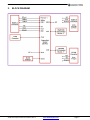
SUMIT-ISM / FEATUREPAK
ADAPTER MODULE
User Manual
Revision A
Revision
Date
Comment
A
4/25/11
Initial Release
FOR TECHNICAL SUPPORT
PLEASE CONTACT:
[email protected]
April 2011
Copyright 2011
Diamond Systems Corporation
555 Ellis Street
Mountain View, CA 94043 USA
Tel 1-650-810-2500
Fax 1-650-810-2525
www.diamondsystems.com
CONTENTS
Important Safe-Handling Information .....................................................................................................................3
1. Description ........................................................................................................................................................4
1.1 Features .........................................................................................................................................................4
1.2 SUMIT and FeaturePak Resources...............................................................................................................4
2. Block Diagram ...................................................................................................................................................5
3. Mechanical Drawing .........................................................................................................................................6
4. Functional Description .....................................................................................................................................6
5. Connectors and Jumpers ................................................................................................................................7
5.1 FeaturePak Connector, J13 ...........................................................................................................................7
5.2 I/O Connectors, J3 and J5 .............................................................................................................................8
5.3 JTAG Connector, J6 ......................................................................................................................................8
5.4 PC/104 Connector, J1 and J2 .......................................................................................................................9
5.5 SUMIT A and SUMIT B Connectors, J9 and J11 ....................................................................................... 10
5.6 Power Connector, J16 ................................................................................................................................ 11
5.7 Slot ID Selector Jumper Block, J4 .............................................................................................................. 11
SUMIT/FP Adapter Module User Manual Rev A
www.diamondsystems.com
Page 2
IMPORTANT SAFE-HANDLING INFORMATION
WARNING: ESD-Sensitive Electronic Equipment!
Observe ESD-safe handling procedures when working with this product.
Always use this product in a properly grounded work area and wear
appropriate ESD-preventive clothing and/or accessories.
Always store this product in ESD-protective packaging when not in use.
Safe Handling Precautions
Aurora contains numerous I/O connectors that connect to sensitive electronic components. This creates many
opportunities for accidental damage during handling, installation and connection to other equipment. The list here
describes common causes of failure found on boards returned to Diamond Systems for repair. This information is
provided as a source of advice to help you prevent damaging your Diamond (or any vendor‟s) embedded
computer boards.
ESD damage – This type of damage is almost impossible to detect, because there is no visual sign of failure or
damage. The symptom is that the board simply stops working, because some component becomes defective.
Usually the failure can be identified and the chip can be replaced.
To prevent ESD damage, always follow proper ESD-prevention practices when handling computer boards.
Damage during handling or storage – On some boards we have noticed physical damage from mishandling. A
common observation is that a screwdriver slipped while installing the board, causing a gouge in the PCB surface
and cutting signal traces or damaging components.
Another common observation is damaged board corners, indicating the board was dropped. This may or may not
cause damage to the circuitry, depending on what is near the corner. Most of our boards are designed with at
least 25 mils clearance between the board edge and any component pad, and ground / power planes are at least
20 mils from the edge to avoid possible shorting from this type of damage. However these design rules are not
sufficient to prevent damage in all situations.
A third cause of failure is when a metal screwdriver tip slips, or a screw drops onto the board while it is powered
on, causing a short between a power pin and a signal pin on a component. This can cause overvoltage / power
supply problems described below. To avoid this type of failure, only perform assembly operations when the
system is powered off.
Sometimes boards are stored in racks with slots that grip the edge of the board. This is a common practice for
board manufacturers. However our boards are generally very dense, and if the board has components very close
to the board edge, they can be damaged or even knocked off the board when the board tilts back in the rack.
Diamond recommends that all our boards be stored only in individual ESD-safe packaging. If multiple boards are
stored together, they should be contained in bins with dividers between boards. Do not pile boards on top of each
other or cram too many boards into a small location. This can cause damage to connector pins or fragile
components.
Power supply wired backwards – Our power supplies and boards are not designed to withstand a reverse
power supply connection. This will destroy each IC that is connected to the power supply. In this case the board
will most likely will be unrepairable and must be replaced. A chip destroyed by reverse power or by excessive
power will often have a visible hole on the top or show some deformation on the top surface due to vaporization
inside the package. Check twice before applying power!
Bent connector pins – This type of problem is often only a cosmetic issue and is easily fixed by bending the pins
back to their proper shape one at a time with needle-nose pliers. This situation can occur when pulling a ribbon
cable off of a pin header. Note: If the pins are bent too severely, bending them back can cause them to weaken
unacceptably or even break, and the connector must be replaced.
SUMIT/FP Adapter Module User Manual Rev A
www.diamondsystems.com
Page 3
1.
DESCRIPTION
The SUMIT/FP Adapter Module allows the use of FeaturePak
TM
SUMIT-ISM expansion stack locations.
TM
I/O expansion modules in systems that provide
The FeaturePak socket on the SUMIT/FP Adapter consumes a single PCI Express x1 lane from the SUMIT-A bus
connector on the SUMIT-ISM module. The adapter provides a pair of 50-pin I/O header connectors for convenient
access to all FeaturePak I/O. In addition, it includes pass-through connectors for the SUMIT-ISM stack's SUMIT-B
TM
o
o
bus and PC/104 (ISA) bus. An extended operation temperature range of -40 C to +85 C is supported.
1.1
Features
Key SUMIT/FP Adapter features include:
Adds a FeaturePak socket to SUMIT-ISM stacks
Conforms to SUMIT-ISM Type 1 standards
Provides SUMIT-A and SUMIT-B bus passthrough
Provides PC/104 (ISA) bus passthrough
Routes 1 PCIe, 1 USB, SMBus, and power/ground from SUMIT-A to the FeaturePak socket
Lane-shifts PCIe and USB on the SUMIT bus
Provides 2 50-pin headers for FeaturePak user I/O
o
o
Supports -40 C to +85 C operating temperature range
For more information about the FeaturePak specification, please refer to the FeaturePak website at
http://www.featurepak.org. For more information on the SUMIT-ISM standard, please refer to www.sffsig.org/sumit.html.
1.2
SUMIT and FeaturePak Resources
The SUMIT/FP Adapter uses the SUMIT and FeaturePak resources indicated in the tables below.
SUMIT/FP Adapter Module User Manual Rev A
www.diamondsystems.com
Page 4
2.
BLOCK DIAGRAM
SUMIT/FP Adapter Module User Manual Rev A
www.diamondsystems.com
Page 5
3.
MECHANICAL DRAWING
The SUMIT/FP Adapter Module complies with the SUMIT-ISM Specification v1.0.
All I/O connectors are located on the board so that there is sufficient room to install all connectors without
interference from any other connector or mounting hole. There are two mounting holes to secure the FeaturePak
module to the SUMIT/FP Adapter Module.
4.
FUNCTIONAL DESCRIPTION
The SUMIT/FP Adapter Module is a FeaturePak baseboard in the SUMIT-ISM Type I form factor. It contains a
FeaturePak MXM socket, a JTAG header, and two 50-pin I/O connectors. Power is provided through both the
SUMIT and PC/104 (ISA) bus connectors.
SUMIT-A and SUMIT-B connectors are present on both the top and bottom side of the board, forming a stacking
high-speed bus with good signal integrity and EMI properties. USB ports and PCIe lanes from the SUMIT-A and
SUMIT-B connectors that are not used by the FeaturePak connector are lane-shifted according to the figures in
the SUMIT Specification v1.5 or later. All other unused signals are passed directly from the bottom side of the
SUMIT-A and –B connectors to the identical pin numbers of the top side connectors. Multi-drop buses like LPC
and SMBus are routed to the top and bottom side of the SUMIT connectors, and to the FeaturePak socket. The
SUMIT/FP Adapter consumes one PCIe lane and one USB port.
SUMIT/FP Adapter Module User Manual Rev A
www.diamondsystems.com
Page 6
5.
CONNECTORS AND JUMPERS
All of the following connectors are on the top side of the board. Connector and pinout information is provided in
the following sections.
5.1
FeaturePak Connector, J13
The SUMIT/FP Adapter Module typically comes with a FeaturePak module installed in the FeaturePak connector.
The inserted FeaturePak module defines the signals that are provided to the user. The FeaturePak connector,
J13, is a compact MXM connector that provides 230 contacts organized into two rows of 115 contacts, with
0.5mm pitch. The connector is rated for 2.5Gbps operation, making it suitable for PCI Express, USB, and other
high speed signals. It contains an alignment pin to ensure proper orientation of the FeaturePak module during
insertion. The alignment pin is the primary reference point for the relative position of the module and the
connector.
FeaturePak Connector Pinout
+3.3V
+3.3V
Ground
PCIe-TX1+
PCIe-TX1Ground
PCIe-CLK1+
PCIe-CLK1Ground
PCIe-TX2+
PCIe-TX2Ground
PCIe-ResetLPC-SERIRQ
LPC-ResetLPC-AD3
LPC-AD1
Ground
USB-Ch1+
USB-Ch1Ground
+3.3V
+3.3V
Serial-TX1
Serial-RTS1
SMBalert#
Slot ID 2
Slot ID 0
JTAG-TDI
JTAG-CLK
Sys-Reset+3.3V
+3.3V
Reserved
Reserved
+3.3V
Reserved
Reserved
+3.3V
Reserved
Reserved
Reserved
Reserved
1
3
5
7
9
11
13
15
17
19
21
23
25
27
29
31
33
35
37
39
41
43
45
47
49
51
53
55
57
59
61
63
65
67
69
71
73
75
77
79
81
83
85
2
4
6
8
10
12
14
16
18
20
22
24
26
28
30
32
34
36
38
40
42
44
46
48
50
52
54
56
58
60
62
64
66
68
70
72
74
76
78
80
82
84
86
+12V
PS-Current
Ground
PCIe-RX1+
PCIe-RX1Ground
PCIe-CLK2+
PCIe-CLK2Ground
PCIe-RX2+
PCIe-RX2Ground
LPC-CLK
LPC-DRQ
LPC-FrameLPC-AD2
LPC-AD0
Ground
USB-Ch2+
USB-Ch2Ground
USB-OC1/2Serial-RX1
Serial-CTS1
SMBclk
SMBdata
Slot ID 1
PresentJTAG-TDO
JTAG-TMS
Reserved
Ground
Ground
Reserved
Reserved
Ground
Reserved
Reserved
Ground
Reserved
Reserved
Reserved
Reserved
SUMIT/FP Adapter Module User Manual Rev A
+5V
+5V
I/OB-50
I/OB-48
I/OB-46
I/OB-44
I/OB-42
I/OB-40
I/OB-38
I/OB-36
I/OB-34
I/OB-32
I/OB-30
I/OB-28
I/OB-26
I/OB-24
I/OB-22
I/OB-20
I/OB-18
I/OB-16
I/OB-14
I/OB-12
I/OB-10
I/OB-8
I/OB-6
I/OB-4
I/OB-2
87
89
91
93
95
97
99
101
103
105
107
109
111
113
115
117
119
121
123
125
127
129
131
133
135
137
139
88
90
92
94
96
98
100
102
104
106
108
110
112
114
116
118
120
122
124
126
128
130
132
134
136
138
140
Ground
Ground
I/OB-49
I/OB-47
I/OB-45
I/OB-43
I/OB-41
I/OB-39
I/OB-37
I/OB-35
I/OB-33
I/OB-31
I/OB-29
I/OB-27
I/OB-25
I/OB-23
I/OB-21
I/OB-19
I/OB-17
I/OB-15
I/OB-13
I/OB-11
I/OB-9
I/OB-7
I/OB-5
I/OB-3
I/OB-1
www.diamondsystems.com
+5V
+5V
+5V
I/OA-50
I/OA-48
I/OA-46
I/OA-44
I/OA-42
I/OA-40
I/OA-38
I/OA-36
(NC)
I/OA-34
(NC)
I/OA-32
(NC)
I/OA-30
(NC)
I/OA-28
(NC)
I/OA-26
(NC)
I/OA-24
(NC)
I/OA-22
(NC)
I/OA-20
(NC)
I/OA-18
(NC)
I/OA-16
(NC)
I/OA-14
(NC)
I/OA-12
(NC)
I/OA-10
(NC)
I/OA-8
(NC)
I/OA-6
(NC)
I/OA-4
(NC)
I/OA-2
141
143
145
147
149
151
153
155
157
159
161
163
165
167
169
171
173
175
177
179
181
183
185
187
189
191
193
195
197
199
201
203
205
207
209
211
213
215
217
219
221
223
225
227
229
142
144
146
148
150
152
154
156
158
160
162
164
166
168
170
172
174
176
178
180
182
184
186
188
190
192
194
196
198
200
202
204
206
208
210
212
214
216
218
220
222
224
226
228
230
Ground
Ground
Ground
I/OA-49
I/OA-47
I/OA-45
I/OA-43
I/OA-41
I/OA-39
I/OA-37
I/OA-35
(NC)
I/OA-33
(NC)
I/OA-31
(NC)
I/OA-29
(NC)
I/OA-27
(NC)
I/OA-25
(NC)
I/OA-23
(NC)
I/OA-21
(NC)
I/OA-19
(NC)
I/OA-17
(NC)
I/OA-15
(NC)
I/OA-13
(NC)
I/OA-11
(NC)
I/OA-9
(NC)
I/OA-7
(NC)
I/OA-5
(NC)
I/OA-3
(NC)
I/OA-1
Page 7
5.2
I/O Connectors, J3 and J5
The FeaturePak I/O signals are brought out to two connectors: Port A and Port B. Port A is labeled as J3 on the
PBC, and Port B is labeled as J5. Each port I/O connector is a .1” dual row 50-pin male right angle connector.
The pins from the FeaturePak connector are brought out to the Port A and Port B connectors as defined in the
following table.
FeaturePak
Connector Pin
5.3
Port A
FeaturePak
Pin
Connector Pin
FeaturePak
Connector Pin
Port B FeaturePak
Pin
Connector Pin
230
1
2
229
140
1
2
139
226
3
4
225
138
3
4
137
222
5
6
221
136
5
6
135
218
7
8
217
134
7
8
133
214
9
10
213
132
9
10
131
210
11
12
209
130
11
12
129
206
13
14
205
128
13
14
127
202
15
16
201
126
15
16
125
198
17
18
197
124
17
18
123
19
20
121
194
19
20
193
122
190
21
22
189
120
21
22
119
186
23
24
185
118
23
24
117
182
25
26
181
116
25
26
115
178
27
28
177
114
27
28
113
174
29
30
173
112
29
30
111
170
31
32
169
110
31
32
109
166
33
34
165
108
33
34
107
162
35
36
161
106
35
36
105
160
37
38
159
104
37
38
103
158
39
40
157
102
39
40
101
156
41
42
155
100
41
42
99
154
43
44
153
98
43
44
97
45
46
95
152
45
46
151
96
150
47
48
149
94
47
48
93
148
49
50
147
92
49
50
91
JTAG Connector, J6
The JTAG connector, J6, passes the defined signals to their equivalent on the FeaturePak connector, enabling an
installed FeaturePak module to be reprogrammed. This is a standard .1” 6-pin single row straight pin header
connector with gold flash plating.
+3.3V
Ground
JTAG-CLK
JTAG-TDO
JTAG-TD1
JTAG-TMS
1
2
3
4
5
6
SUMIT/FP Adapter Module User Manual Rev A
www.diamondsystems.com
Page 8
5.4
PC/104 Connector, J1 and J2
The PC/104 bus is essentially identical to the ISA Bus except for the physical design. It specifies two pin and
socket connectors for the bus signals. A 64-pin header, J1, incorporates the 62-pin 8-bit bus connector signals,
and a 40-pin header, J2, incorporates the 36-pin 16-bit bus connector signals. The additional pins on the PC/104
connectors are used as ground or key pins. The female sockets on the top of the board enable stacking another
PC/104 board on top of the board, while the male pins on the bottom enable the board to plug into another board
below it.
In the pinout figures below, the tops correspond to the left edge of the connector when the board is viewed from
the primary side (side with the female end of the PC/104 connector) and the board is oriented so that the PC/104
connectors are along the bottom edge of the board.
For more information on the PC/104 specification, visit the PC/104 Embedded Consortium website, at
http://www.pc104.org.
View from Top of Board
J1, PC/104 8-bit bus connector
IOCHK-
A1
B1
SD7
A2
B2
SD6
A3
B3
SD5
A4
B4
SD4
A5
B5
SD3
A6
B6
SD2
A7
B7
SD1
A8
B8
SD0
A9
B9
+12V
IOCHRDY
A10
B10
KEY
AEN
A11
B11
SMEMW-W
SA19
A12
B12
SMEMR-
SA18
A13
B13
SA17
A14
SA16
J2, PC/104 16-bit bus connector
Ground
C0
D0
Ground
MEMCS16
C1
D1
SBHE-
IOCS16--
C2
D2
LA23
IRQ10
C3
D3
LA22
IRQ11
C4
D4
LA21
IRQ12
C5
D5
LA20
-12V
IRQ15
C6
D6
LA19
OWS-
IRQ14
C7
D7
LA18
DACK0-
C8
D8
LA17
DRQ0
C9
D9
MEMR-
DACK5-
C10
D10
MEMW-
DRQ5
C11
D11
SD8
IOW-
DACK6-
C12
D12
SD9
B14
IOR-
DRQ6
C13
D13
SD10
A15
B15
DACK3-
DACK7-
C14
D14
SD11
SA15
A16
B16
DRQ3
DRQ7
C15
D15
SD12
SA14
A17
B17
DACK1-
+5V
C16
D16
SD13
SA13
A18
B18
DRQ1
MASTER-
C17
D17
SD14
SA12
A19
B19
Ground
C18
D18
SD15
SA11
A20
B20
SYSCLK
Ground
C19
D19
KEY
SA10
A21
B21
IRQ7
SA9
A22
B22
IRQ6
SA8
A23
B23
IRQ5
SA7
A24
B24
IRQ4
SA6
A25
B25
IRQ3
SA5
A26
B26
DACK2-
SA4
A27
B27
TC
SA3
A28
B28
BALE
SA2
A29
B29
+5V
SA1
A30
B30
OSC
SA0
A31
B31
Ground
Ground
A32
B32
Ground
Ground
RESET
+5V
IRQ9
-5V
DRQ2
REFRESH-
SUMIT/FP Adapter Module User Manual Rev A
www.diamondsystems.com
Page 9
5.5
SUMIT A and SUMIT B Connectors, J9 and J11
The SUMIT stackable bus consists of two 52-pin connectors; SUMIT-A, labeled J11, and SUMIT-B, labeled J9.
The SUMIT/FP Adapter Module consumes one PCIe lane and one USB port.
The standard signal assignments of the SUMIT-A and -B connectors appear in below. For more information on
the SUMIT specification, visit the SFF-SIG website at http://www.sff-sig.org.
SUMIT-A Connector (J11)
+5VSB
1
2
+12V
3.3V
3
4
3.3V
5
EXPCD_REQ#
SUMIT-B Connector (J9)
GND
1
2
GND
SMB _DATA
B_PETp0
3
4
B_PERp0
6
SMB_CLK
B_PETn0
5
6
B_PERn0
7
8
SMB_ALERT#
GND
7
8
BPRSNT#/GND
EXPCD_PRSNT#
9
10
SPI/uWire_DO
C_CLKp
9
10
B_CLKp
USB_OC#
11
12
SPI/uWire_DI
C_CLKn
11
12
B_CLKn
RSVD
13
14
SPI/uWire_CLK
CPRSNT#/GND
13
14
GND
+5V
15
16
SPI/uWire_CS0#
C_PETp0
15
16
C_PERp0
USB3+
17
18
SPI/uWire_CS1#
C_PETn0
17
18
C_PERn0
USB3-
19
20
RSVD
GND
19
20
GND
+5V
21
22
LPC_DRQ
C_PETp1
21
22
C_PERp1
USB2+
23
24
LPC_AD0
C_PETn1
23
24
C_PERn1
USB2-
25
26
LPC_AD1
GND
25
26
GND
+5V
27
28
LPC_AD2
C_PETp2
27
28
C_PERp2
USB1+
29
30
LPC_AD3
C_PETn2
29
30
C_PERn2
USB1-
31
32
LPC_FRAME#
GND
31
32
GND
+5V
33
34
SERIRQ#
C_PETp3
33
34
C_PERp3
USB0+
35
36
LPC_PRSNT#/GND
C_PETn3
35
36
C_PERn3
USB0-
37
38
CLK_33MHz
GND
37
38
GND
GND
39
40
GND
PERST#
39
40
WAKE#
A_PETp0
41
42
A_PERp0
RSVD
41
42
RSVD
A_PETn0
43
44
A_PERn0
+5V
43
44
RSVD
GND
45
46
APRSNT#/GND
+5V
45
46
3.3V
PERST#
47
48
A_CLKp
+5V
47
48
3.3V
WAKE#
49
50
A_CLKn
+5V
49
50
3.3V
+5V
51
52
GND
+5V
51
52
+5VSB
These two surface-mounted 52-pin connectors are located on the expansion side of the board. Their mechanical
requirements, pin-out, and signal functionality complies with the SFF-SIG's “SUMIT” and “SUMIT-ISM”
specifications, available from the SFF-SIG (http://sff-sig.org/sumit.html).
SUMIT/FP Adapter Module User Manual Rev A
www.diamondsystems.com
Page 10
5.6
Power Connector, J16
The power connector, J16, provides a means to bring external +5VDC and +3.3VDC power to the adapter,
powering the board. This is an alternate method that can be used to power the adapter as opposed to powering it
through the PC/104 connector. This is a standard .1” 3-pin single row right angle pin header connector with gold
flash plating.
+5V
+3.3V
Ground
5.7
1
2
3
Slot ID Selector Jumper Block, J4
The Slot ID Selector jumper block, J4, determines the slot ID of the board. The slot ID bits are identified on the
board as Slot ID 2, 1, or 0. The three slot ID bits are pulled up or down through jumpers as follows: „0‟ = ground,
„1‟ = +3.3V. The default Slot ID is 001 as shown in the table below.
Slot ID:
2
1
О
О
О
О
0
PC/104™ is a trademark of the PC/104 Embedded Consortium. SUMIT™ is a trademark of the SFF-SIG. FeaturePak™ is a trademark of the
FeaturePak Trade Association. All other trademarks are the property of their respective owners.
SUMIT/FP Adapter Module User Manual Rev A
www.diamondsystems.com
Page 11