1
Spartan-3
Starter Kit Board
User Guide
UG130 (v1.1) May 13, 2005
R
R
6
Preface: About This Guide
www.xilinx.com
1-800-255-7778
Spartan-3 Starter Kit Board User Guide
UG130 (v1.1) May 13, 2005
R
Chapter 1
Introduction
The Xilinx Spartan-3 Starter Kit provides a low-cost, easy-to-use development and
evaluation platform for Spartan-3 FPGA designs.
Key Components and Features
Figure 1-1 shows the Spartan-3 Starter Kit board, which includes the following
components and features:
•
•
•
200,000-gate Xilinx Spartan-3 XC3S200 FPGA in a 256-ball thin Ball Grid Array
package (XC3S200FT256) 1
♦
4,320 logic cell equivalents
♦
Twelve 18K-bit block RAMs (216K bits)
♦
Twelve 18x18 hardware multipliers
♦
Four Digital Clock Managers (DCMs)
♦
Up to 173 user-defined I/O signals
2Mbit Xilinx XCF02S Platform Flash, in-system programmable configuration
PROM 2
♦
1Mbit non-volatile data or application code storage available after FPGA
configuration
♦
Jumper options allow FPGA application to read PROM data or FPGA
configuration from other sources 3
1M-byte of Fast Asynchronous SRAM (bottom side of board, see Figure 1-3)
♦
Two 256Kx16 ISSI IS61LV25616AL-10T 10 ns SRAMs
♦
Configurable memory architecture
-
Single 256Kx32 SRAM array, ideal for MicroBlaze code images
-
Two independent 256Kx16 SRAM arrays
♦
Individual chip select per device
♦
Individual byte enables
•
3-bit, 8-color VGA display port
•
9-pin RS-232 Serial Port
4
5
6
♦
DB9 9-pin female connector (DCE connector)
♦
RS-232 transceiver/level translator
♦
Uses straight-through serial cable to connect to computer or workstation serial
port
♦
Second RS-232 transmit and receive channel available on board test points
Spartan-3 Starter Kit Board User Guide
UG130 (v1.1) May 13, 2005
www.xilinx.com
1-800-255-7778
7
8
7
R
Chapter 1: Introduction
Digilent Low-Cost 23
Parallel Port to JTAG Included
Cable
Parallel Cable IV 24
MutliPro Desktop Tool
JTAG Connector
Low-Cost JTAG
Download Cable
Connector
22
A1 Expansion
Header
21
XCF02S 2Mbit
Configuration
PROM
A2 Expansion
Header
20
Platform Flash
Option Jumpers
B1 Expansion
Header
19
256Kx16
10ns SRAM
Configuration
DONE LED
18
PROGRAM
Push Button
17
Configuration
Mode Select
Jumpers
16
2
3
4
1
256Kx16
10ns SRAM
5
8-color
VGA Port
6
RS-232 Port
Serial Port
XC3S200
Spartan-3
FPGA
7
9
RS-232
Driver
Auxiliary 15
Oscillator Socket
PS/2 Port
50 MHz
Oscillator
4 Character
7-Segment LED
14
10
11
13
4 Push Buttons
8 Slide Switches
8 LEDs
12
VCCO
Power On
LED
26
3.3V 27
Regulator
2.5V 28
Regulator
1.2V 29
Regulator
5 VDC, 2A Supply
AC Wall Adapter
100-240V AC Input Included
50-60 Hz 25
UG130_c1_01_042504
Figure 1-1: Xilinx Spartan-3 Starter Kit Board Block Diagram
8
•
PS/2-style mouse/keyboard port
•
Four-character, seven-segment LED display
•
Eight slide switches
•
Eight individual LED outputs
•
Four momentary-contact push button switches
9
10
11
12
www.xilinx.com
1-800-255-7778
13
Spartan-3 Starter Kit Board User Guide
UG130 (v1.1) May 13, 2005
R
Component Locations
•
50 MHz crystal oscillator clock source (bottom side of board, see Figure 1-3)
•
Socket for an auxiliary crystal oscillator clock source
•
FPGA configuration mode selected via jumper settings
•
Push button switch to force FPGA reconfiguration (FPGA configuration happens
automatically at power-on) 17
•
LED indicates when FPGA is successfully configured
•
Three 40-pin expansion connection ports to extend and enhance the Spartan-3 Starter
Kit Board 19 20 21
14
15
16
18
♦
See www.xilinx.com/s3boards for compatible expansion cards
♦
Compatible with Digilent, Inc. peripheral boards
https://digilent.us/Sales/boards.cfm#Peripheral
♦
FPGA serial configuration interface signals available on the A2 and B1 connectors
-
PROG_B, DONE, INIT_B, CCLK, DONE
•
JTAG port
•
Digilent JTAG download/debugging cable connects to PC parallel port
•
JTAG download/debug port compatible with the Xilinx Parallel Cable IV and
MultiPRO Desktop Tool 24
•
AC power adapter input for included international unregulated +5V power
supply 25
•
Power-on indicator LED
26
•
On-board 3.3V
28
22
for low-cost download cable
27
, 2.5V
, and 1.2V
29
23
23
regulators
Component Locations
Figure 1-2 and Figure 1-3 indicate the component locations on the top side and bottom side
of the board, respectively.
Spartan-3 Starter Kit Board User Guide
UG130 (v1.1) May 13, 2005
www.xilinx.com
1-800-255-7778
9
R
Chapter 1: Introduction
21
20
A1 Expansion Connector
A2 Expansion Connector
31
2
27
24
VGA
16
17
3
XILINX
XC3S200
FPGA
18
DONE
25
19
2Mbit
PlatformFlash
B1 Expansion Connector
3.3V
22
5
PROG
1
POWER
POWER
26
RS-232
RS-232
6
7
15
10
12
30
8
PS/2
9
11
13
ug130_c1_02_042704
Figure 1-2: Xilinx Spartan-3 Starter Kit Board (Top Side)
5
256Kx16
SRAM
256Kx16
SRAM
4
2.5V
28
29
50
MHz
1.2V
14
6
ug130_c1_03_042704
Figure 1-3: Xilinx Spartan-3 Starter Kit Board (Bottom Side)
10
www.xilinx.com
1-800-255-7778
Spartan-3 Starter Kit Board User Guide
UG130 (v1.1) May 13, 2005
R
Chapter 3
Four-Digit, Seven-Segment LED Display
The Spartan-3 Starter Kit board has a four-character, seven segment LED display
controlled by FPGA user-I/O pins, as shown in Figure 3-1. Each digit shares eight common
control signals to light individual LED segments. Each individual character has a separate
anode control input. A detailed schematic for the display appears in Figure A-2.
The pin number for each FPGA pin connected to the LED display appears in parentheses.
To light an individual signal, drive the individual segment control signal Low along with
the associated anode control signal for the individual character. In Figure 3-1, for example,
the left-most character displays the value ‘2’. The digital values driving the display in this
example are shown in blue. The AN3 anode control signal is Low, enabling the control
inputs for the left-most character. The segment control inputs, A through G and DP, drive
the individual segments that comprise the character. A Low value lights the individual
segment, a High turns off the segment. A Low on the A input signal, lights segment ‘a’ of
the display. The anode controls for the remaining characters, AN[2:0] are all High, and
these characters ignore the values presented on A through G and DP.
AN3 (E13)
AN2 (F14)
0
AN1 (G14)
1
AN0 (D14)
1
1
(E14)
a
a
0
A
0
B
1
C
(N16)
0
D
g
0
E
1
F
0
G
1 DP
(F13)
(R16)
f
b
(G13)
f
a
b
f
g
e
c
d
(N15)
dp
e
b
f
g
c
d
a
e
dp
b
g
c
d
e
dp
c
d
dp
(P15)
(P16)
UG130_c3_01_042704
Figure 3-1: Seven-Segment LED Digit Control
Table 3-1 lists the FPGA connections that drive the individual LEDs comprising a sevensegment character. Table 3-2 lists the connections to enable a specific character. Table 3-3
shows the patterns required to display hexadecimal characters.
Spartan-3 Starter Kit Board User Guide
UG130 (v1.1) May 13, 2005
www.xilinx.com
1-800-255-7778
15
R
Chapter 3: Four-Digit, Seven-Segment LED Display
Table 3-1: FPGA Connections to Seven-Segment Display (Active Low)
Segment
FPGA Pin
A
E14
B
G13
C
N15
D
P15
E
R16
F
F13
G
N16
DP
P16
Table 3-2: Digit Enable (Anode Control) Signals (Active Low)
Anode Control
AN3
AN2
AN1
AN0
FPGA Pin
E13
F14
G14
D14
Table 3-3: Display Characters and Resulting LED Segment Control Values
16
Character
a
b
c
d
e
f
g
0
0
0
0
0
0
0
1
1
1
0
0
1
1
1
1
2
0
0
1
0
0
1
0
3
0
0
0
0
1
1
0
4
1
0
0
1
1
0
0
5
0
1
0
0
1
0
0
6
0
1
0
0
0
0
0
7
0
0
0
1
1
1
1
8
0
0
0
0
0
0
0
9
0
0
0
0
1
0
0
A
0
0
0
1
0
0
0
b
1
1
0
0
0
0
0
C
0
1
1
0
0
0
1
d
1
0
0
0
0
1
0
E
0
1
1
0
0
0
0
F
0
1
1
1
0
0
0
www.xilinx.com
1-800-255-7778
Spartan-3 Starter Kit Board User Guide
UG130 (v1.1) May 13, 2005
R
The LED control signals are time-multiplexed to display data on all four characters, as
shown in Figure 3-2. Present the value to be displayed on the segment control inputs and
select the specified character by driving the associated anode control signal Low. Through
persistence of vision, the human brain perceives that all four characters appear
simultaneously, similar to the way the brain perceives a TV display.
AN3
AN2
AN1
AN0
{A,B,C,D,E,F,G,DP}
DISP3
DISP2
DISP1
DISP0
UG130_c3_02_042404
Figure 3-2: Drive Anode Input Low to Light an Individual Character
This “scanning” technique reduces the number of I/O pins required for the four
characters. If an FPGA pin were dedicated for each individual segment, then 32 pins are
required to drive four 7-segment LED characters. The scanning technique reduces the
required I/O down to 12 pins. The drawback to this approach is that the FPGA logic must
continuously scan data out to the displays—a small price to save 20 additional I/O pins.
Spartan-3 Starter Kit Board User Guide
UG130 (v1.1) May 13, 2005
www.xilinx.com
1-800-255-7778
17
R
18
Chapter 3: Four-Digit, Seven-Segment LED Display
www.xilinx.com
1-800-255-7778
Spartan-3 Starter Kit Board User Guide
UG130 (v1.1) May 13, 2005
R
Chapter 4
Switches and LEDs
Slide Switches
The Spartan-3 Starter Kit board has eight slide switches, indicated as 11 in Figure 1-2. The
switches are located along the lower edge of the board, toward the right edge. The switches
are labeled SW7 through SW0. Switch SW7 is the left-most switch, and SW0 is the rightmost switch. The switches connect to an associated FPGA pin, as shown in Table 4-1. A
detailed schematic appears in Figure A-2.
Table 4-1: Slider Switch Connections
Switch
SW7
SW6
SW5
SW4
SW3
SW2
SW1
SW0
FPGA Pin
K13
K14
J13
J14
H13
H14
G12
F12
When in the UP or ON position, a switch connects the FPGA pin to VCCO, a logic High.
When DOWN or in the OFF position, the switch connects the FPGA pin to ground, a logic
Low. The switches typically exhibit about 2 ms of mechanical bounce and there is no active
debouncing circuitry, although such circuitry could easily be added to the FPGA design
programmed on the board. A 4.7KΩ series resistor provides nominal input protection.
Push Button Switches
The Spartan-3 Starter Kit board has four momentary-contact push button switches,
indicated as 13 in Figure 1-2. These push buttons are located along the lower edge of the
board, toward the right edge. The switches are labeled BTN3 through BTN0. Push button
switch BTN3 is the left-most switch, BTN0 the right-most switch. The push button
switches connect to an associated FPGA pin, as shown in Table 4-2. A detailed schematic
appears in Figure A-2.
Table 4-2: Push Button Switch Connections
Push Button
BTN3 (User Reset)
BTN2
BTN1
BTN0
FPGA Pin
L14
L13
M14
M13
Pressing a push button generates a logic High on the associated FPGA pin. Again, there is
no active debouncing circuitry on the push button.
The left-most button, BTN3, is also the default User Reset pin. BTN3 electrically behaves
identically to the other push buttons. However, when applicable, BTN3 resets the provided
reference designs.
Spartan-3 Starter Kit Board User Guide
UG130 (v1.1) May 13, 2005
www.xilinx.com
1-800-255-7778
19
R
Chapter 4: Switches and LEDs
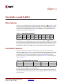
LEDs
The Spartan-3 Starter Kit board has eight individual surface-mount LEDs located above
the push button switches, indicated by 12 in Figure 1-2. The LEDs are labeled LED7
through LED0. LED7 is the left-most LED, LED0 the right-most LED. Table 4-3 shows the
FPGA connections to the LEDs.
Table 4-3: LED Connections to the Spartan-3 FPGA
LED
LD7
LD6
LD5
LD4
LD3
LD2
LD1
LD0
FPGA Pin
P11
P12
N12
P13
N14
L12
P14
K12
The cathode of each LED connects to ground via a 270Ω resistor. To light an individual
LED, drive the associated FPGA control signal High, which is the opposite polarity from
lighting one of the 7-segment LEDs.
20
www.xilinx.com
1-800-255-7778
Spartan-3 Starter Kit Board User Guide
UG130 (v1.1) May 13, 2005
R
Chapter 5
VGA Port
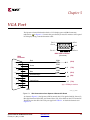
The Spartan-3 Starter Kit board includes a VGA display port and DB15 connector,
indicated as 5 in Figure 1-2. Connect this port directly to most PC monitors or flat-panel
LCD displays using a standard monitor cable.
Pin 5
Pin 1
Pin 10
Pin 6
Pin 15
Pin 11
DB15 VGA Connector
(front view)
DB15
Connector
270Ω
Red
1
6
11
(R12)
G
(T12)
B
(R11)
270Ω
Green
2
7
12
R
270Ω
Blue
3
8
Horizontal Sync
HS (R9)
13
4
9
Vertical Sync
VS
14
(T10)
5
(xx) = FPGA pin number
10
15
GND
UG130_c5_01_042604
Figure 5-1: VGA Connections from Spartan-3 Starter Kit Board
As shown in Figure 5-1, the Spartan-3 FPGA controls five VGA signals: Red (R), Green (G),
Blue (B), Horizontal Sync (HS), and Vertical Sync (VS), all available on the VGA connector.
The FPGA pins that drive the VGA port appear in Table 5-1. A detailed schematic is in
Figure A-7.
Spartan-3 Starter Kit Board User Guide
UG130 (v1.1) May 13, 2005
www.xilinx.com
1-800-255-7778
21
R
Chapter 5: VGA Port
Table 5-1: VGA Port Connections to the Spartan-3 FPGA
Signal
FPGA Pin
Red (R)
R12
Green (G)
T12
Blue (B)
R11
Horizontal Sync (HS)
R9
Vertical Sync (VS)
T10
Each color line has a series resistor to provide 3-bit color, with one bit each for Red, Green,
and Blue. The series resistor uses the 75Ω VGA cable termination to ensure that the color
signals remain in the VGA-specified 0V to 0.7V range. The HS and VS signals are TTL level.
Drive the R, G, and B signals High or Low to generate the eight possible colors shown in
Table 5-2.
Table 5-2: 3-Bit Display Color Codes
Red (R)
Green (G)
Blue (B)
Resulting Color
0
0
0
Black
0
0
1
Blue
0
1
0
Green
0
1
1
Cyan
1
0
0
Red
1
0
1
Magenta
1
1
0
Yellow
1
1
1
White
VGA signal timing is specified, published, copyrighted, and sold by the Video Electronics
Standards Association (VESA). The following VGA system and timing information is
provided as an example of how the FPGA might drive VGA monitor in 640 by 480 mode.
For more precise information or for information on higher VGA frequencies, refer to
documents available on the VESA website or other electronics websites:
•
Video Electronics Standards Association
http://www.vesa.org
•
VGA Timing Information
http://www.epanorama.net/documents/pc/vga_timing.html
Signal Timing for a 60Hz, 640x480 VGA Display
CRT-based VGA displays use amplitude-modulated, moving electron beams (or cathode
rays) to display information on a phosphor-coated screen. LCD displays use an array of
switches that can impose a voltage across a small amount of liquid crystal, thereby
changing light permitivity through the crystal on a pixel-by-pixel basis. Although the
following description is limited to CRT displays, LCD displays have evolved to use the
22
www.xilinx.com
1-800-255-7778
Spartan-3 Starter Kit Board User Guide
UG130 (v1.1) May 13, 2005
R
Signal Timing for a 60Hz, 640x480 VGA Display
same signal timings as CRT displays. Consequently, the following discussion pertains to
both CRTs and LCD displays.
Within a CRT display, current waveforms pass through the coils to produce magnetic fields
that deflect electron beams to transverse the display surface in a “raster” pattern,
horizontally from left to right and vertically from top to bottom. As shown in Figure 5-2,
information is only displayed when the beam is moving in the “forward” direction—left to
right and top to bottom—and not during the time the beam returns back to the left or top
edge of the display. Much of the potential display time is therefore lost in “blanking”
periods when the beam is reset and stabilized to begin a new horizontal or vertical display
pass.
pixel 0,0
pixel 0,639
640 pixels are displayed each
time the beam traverses the screen
VGA Display
Current
through the
horizontal
deflection
coil
pixel 479,0
pixel 479,639
Retrace: No
information
is displayed
during
this time
Stable current ramp: Information is
displayed during this time
Total horizontal time
Horizontal display time
time
"back porch"
retrace time
"back porch"
HS
Horizontal sync signal
sets the retrace frequency
"front porch"
UG130_c5_02_051305
Figure 5-2: CRT Display Timing Example
The size of the beams, the frequency at which the beam traces across the display, and the
frequency at which the electron beam is modulated determine the display resolution.
Spartan-3 Starter Kit Board User Guide
UG130 (v1.1) May 13, 2005
www.xilinx.com
1-800-255-7778
23
R
Chapter 5: VGA Port
Modern VGA displays support multiple display resolutions, and the VGA controller
dictates the resolution by producing timing signals to control the raster patterns. The
controller produces TTL-level synchronizing pulses that set the frequency at which current
flows through the deflection coils, and it ensures that pixel or video data is applied to the
electron guns at the correct time.
Video data typically comes from a video refresh memory with one or more bytes assigned
to each pixel location. The Spartan-3 Starter Kit board uses three bits per pixel, producing
one of the eight possible colors shown in Table 5-2. The controller indexes into the video
data buffer as the beams move across the display. The controller then retrieves and applies
video data to the display at precisely the time the electron beam is moving across a given
pixel.
As shown in Figure 5-2, the VGA controller generates the HS (horizontal sync) and VS
(vertical sync) timings signals and coordinates the delivery of video data on each pixel
clock. The pixel clock defines the time available to display one pixel of information. The VS
signal defines the “refresh” frequency of the display, or the frequency at which all
information on the display is redrawn. The minimum refresh frequency is a function of the
display’s phosphor and electron beam intensity, with practical refresh frequencies in the
60 Hz to 120 Hz range. The number of horizontal lines displayed at a given refresh
frequency defines the horizontal “retrace” frequency.
VGA Signal Timing
The signal timings in Table 5-3 are derived for a 640-pixel by 480-row display using a
25 MHz pixel clock and 60 Hz ±1 refresh. Figure 5-3 shows the relation between each of the
timing symbols. The timing for the sync pulse width (TPW) and front and back porch
intervals (TFP and TBP) are based on observations from various VGA displays. The front
and back porch intervals are the pre- and post-sync pulse times. Information cannot be
displayed during these times.
Table 5-3: 640x480 Mode VGA Timing
Symbol
Vertical Sync
Parameter
Horizontal Sync
Time
Clocks
Lines
Time
Clocks
Sync pulse time
16.7 ms
416,800
521
32 µs
800
TDISP
Display time
15.36 ms
384,000
480
25.6 µs
640
TPW
Pulse width
64 µs
1,600
2
3.84 µs
96
TFP
Front porch
320 µs
8,000
10
640 ns
16
TBP
Back porch
928 µs
23,200
29
1.92 µs
48
TS
TS
TFP
TDISP
TBP
TPW
UG130_c5_03_051305
Figure 5-3: VGA Control Timing
24
www.xilinx.com
1-800-255-7778
Spartan-3 Starter Kit Board User Guide
UG130 (v1.1) May 13, 2005
R
VGA Signal Timing
Generally, a counter clocked by the pixel clock controls the horizontal timing. Decoded
counter values generate the HS signal. This counter tracks the current pixel display
location on a given row.
A separate counter tracks the vertical timing. The vertical-sync counter increments with
each HS pulse and decoded values generate the VS signal. This counter tracks the current
display row. These two continuously running counters form the address into a video
display buffer. For example, the on-board fast SRAM is an ideal display buffer.
No time relationship is specified between the onset of the HS pulse and the onset of the VS
pulse. Consequently the counters can be arranged to easily form video RAM addresses, or
to minimize decoding logic for sync pulse generation.
Spartan-3 Starter Kit Board User Guide
UG130 (v1.1) May 13, 2005
www.xilinx.com
1-800-255-7778
25
R
26
Chapter 5: VGA Port
www.xilinx.com
1-800-255-7778
Spartan-3 Starter Kit Board User Guide
UG130 (v1.1) May 13, 2005
R
Chapter 8
Clock Sources
The Spartan-3 Starter Kit board has a dedicated 50 MHz Epson SG-8002JF series clock
oscillator source and an optional socket for another clock oscillator source. Figure A-5
provides a detailed schematic for the clock sources.
The 50 MHz clock oscillator is mounted on the bottom side of the board, indicated as 14
in Figure A-5. Use the 50 MHz clock frequency as is or derive other frequencies using the
FPGAs Digital Clock Managers (DCMs).
•
Using Digital Clock Managers (DCMs) in Spartan-3 FPGAs
http://www.xilinx.com/bvdocs/appnotes/xapp462.pdf
The oscillator socket, indicated as
footprint.
15
in Figure 1-2, accepts oscillators in an 8-pin DIP
Table 8-1: Clock Oscillator Sources
Spartan-3 Starter Kit Board User Guide
UG130 (v1.1) May 13, 2005
Oscillator Source
FPGA Pin
50 MHz (IC4)
T9
Socket (IC8)
D9
www.xilinx.com
1-800-255-7778
35
R
Chapter 9: FPGA Configuration Modes and Functions
Chapter 9
FPGA Configuration Modes and
Functions
FPGA Configuration Mode Settings
In most applications for the Spartan-3 Starter Kit Board, the FPGA automatically boots
from the on-board Platform Flash memory whenever power is applied or the PROG push
button is pressed. However, the board supports all the available configuration modes via
the J8 header, indicated as 16 in Figure 1-2. Table 9-1 provides the available option
settings for the J8 header. Additionally, the JP1 jumper setting is required when using
Master Serial configuration mode, as further described in “Platform Flash Jumper Options
(JP1).”
The default jumper settings for the board are:
•
All jumpers in the J8 header are installed
•
The JP1 jumper is in the “Default” position
Table 9-1: Header J8 Controls the FPGA Configuration Mode
Master Serial
Header J8
Settings
Jumper JP1
Setting
GND J8
JP1
MODE
Configuration
Mode
<M0:M1:M2>
<0:0:0>
M0 M1 M2
GND J8
<1:1:1>
DEFAULT. The FPGA automatically boots from the Platform
Flash.
JP1
JP1
The FPGA attempts to boot from a serial configuration source
attached to either expansion connector A2 or B1.
JP1
Another device connected to either the A2 or B1 expansion
connector provides serial data and clock to load the FPGA.
JP1
The FPGA attempts to boot from a parallel configuration source
attached to the B1 expansion connector.
MODE
Slave Serial
or
Description
M0 M1 M2
GND J8
MODE
Master Parallel
<1:1:0>
M0 M1 M2
36
www.xilinx.com
1-800-255-7778
Spartan-3 Starter Kit Board User Guide
UG130 (v1.1) May 13, 2005
R
Program Push Button/DONE Indicator LED
Table 9-1: Header J8 Controls the FPGA Configuration Mode (Continued)
Slave Parallel
Header J8
Settings
Jumper JP1
Setting
GND J8
JP1
Another device connected to the B1 expansion connector
provides parallel data and clock to load the FPGA.
JP1
The FPGA waits for configuration via the four-wire JTAG
interface.
MODE
Configuration
Mode
<M0:M1:M2>
<0:1:1>
Description
M0 M1 M2
GND J8
MODE
JTAG
<1:0:1>
M0 M1 M2
Program Push Button/DONE Indicator LED
The Spartan-3 Starter Kit Board includes two FPGA configuration functions, located near
the VGA connector and the AC power input connector, as shown in Figure 9-1. The PROG
push button, shown as 17 in Figure 9-1, drives the FPGA’s PROG_B programming pin.
When pressed, the PROG push button forces the FPGA to reconfigure and reload it
configuration data.
VGA
The DONE LED, shown as 18 in Figure 9-1, connects to the FPGA’s DONE pin and lights
up when the FPGA is successfully configured.
VGA
17
18
DONE
PROG
UG130_c9_03_042704
Figure 9-1: The PROG Button and the DONE LED
Spartan-3 Starter Kit Board User Guide
UG130 (v1.1) May 13, 2005
www.xilinx.com
1-800-255-7778
37
R
44
Chapter 11: JTAG Programming/Debugging Ports
www.xilinx.com
1-800-255-7778
Spartan-3 Starter Kit Board User Guide
UG130 (v1.1) May 13, 2005
R
Chapter 12
Power Distribution
AC Wall Adapter
The Spartan-3 Starter Kit includes an international-ready AC wall adapter that produces a
+5V DC output. Connect the AC wall adapter to the barrel connector along the left edge of
the board, indicated as 25 in Figure 1-2. There is no power switch to the board. To
disconnect power, remove the AC adapter from the wall or disconnect the barrel connector.
The POWER indicator LED, shown as 26 in Figure 1-2, lights up when power is properly
applied to the board. If the jumpers in the J8 header and JP1 header are properly set and
there is a valid configuration data file in the Platform Flash memory, then the DONE
indicator LED, shown as 18 in Figure 1-2, also lights up.
The AC wall adapter is directly compatible for North America, Japan, and Taiwan locales.
Other locations might require a socket adapter to convert from the North American
standard to the local power socket standard. The AC wall adapter operates from 100V to
240V AC input, at 50 or 60 Hz.
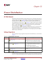
Voltage Regulators
There are multiple voltages supplied on the Spartan-3 Starter Kit Board, as summarized in
Table 12-1.
Table 12-1: Voltage Supplies and Sources
Voltage
+5V DC
Source
Supplies
AC Wall Adapter, 5V switching power supply
( 25 in Figure 1-2)
3.3V regulator
Optionally, PS/2 port via jumper JP2 setting
Pin 1 (VU) on A1, A2, B1 expansion connectors
+3.3V DC
National Semiconductor LM1086CS-ADJ 3.3V
regulator ( 27 in Figure 1-2)
2.5V and 1.2V regulators
VCCO supply input for all FPGA I/O banks
Most components on the board
Pin 3 on A1, A2, B1 expansion connectors
+2.5V DC
STMicroelectronics LF25CDT 2.5V regulator
( 28 in Figure 1-2)
VCCAUX supply input to FPGA
+1.2V DC
Fairchild Semiconductor FAN1112 1.2V
regulator ( 29 in Figure 1-2)
VCCINT supply input to FPGA
Overall, the 5V DC switching power adapter that connects to AC wall power powers the
board. A 3.3V regulator, powered by the 5V DC supply, provides power to the inputs of the
Spartan-3 Starter Kit Board User Guide
UG130 (v1.1) May 13, 2005
www.xilinx.com
1-800-255-7778
45
R
Chapter 12: Power Distribution
2.5V and 1.2V regulators. Similarly, the 3.3V regulator feeds all the VCCO voltage supply
inputs to the FPGA’s I/O banks and powers most of the components on the board.
The 2.5V regulator supplies power to the FPGA’s VCCAUX supply inputs. The VCCAUX
voltage input supplies power to Digital Clock Managers (DCMs) within the FPGA and
supplies some of the I/O structures. In specific, all of the FPGA’s dedicated configuration
pins, such as DONE, PROG_B, CCLK, and the FPGA’s JTAG pins, are powered by VCCAUX.
The FPGA configuration interface on the board is powered by 3.3V. Consequently, the 2.5V
supply has a current shunt resistor to prevent reverse current.
Finally, a 1.2V regulator supplies power to the FPGA’s VCCINT voltage inputs, which
power the FPGA’s core logic.
The board uses three discrete regulators to generate the necessary voltages. However,
various power supply vendors are developing integrated solutions specifically for
Spartan-3 FPGAs.
Figure A-3 provides a detailed schematic of the various voltage regulators. Similarly,
Figure A-6 shows the power decoupling capacitors.
46
www.xilinx.com
1-800-255-7778
Spartan-3 Starter Kit Board User Guide
UG130 (v1.1) May 13, 2005
R
www.xilinx.com/s3boards
PN 0402292
www.xilinx.com
1-800-255-7778
Spartan-3 Starter Kit Board User Guide
UG130 (v1.1) May 13, 2005