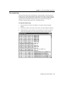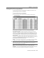
1
OrCAD Layout User’s Guide ® Copyright © 1998 OrCAD, Inc. All rights reserved. OrCAD, OrCAD Capture, OrCAD Layout, and OrCAD PSpice are registered trademarks of OrCAD, Inc. Enterprise CIS, Enterprise Component Information System, OrCAD Capture CIS, OrCAD Express, OrCAD Express CIS, OrCAD Layout Engineer’s Edition, OrCAD Optimizer, and SmartRoute are trademarks of OrCAD, Inc. Microsoft, Visual Basic, Windows, Windows NT, and other names of Microsoft products referenced herein are trademarks or registered trademarks of Microsoft Corporation. All other brand and product names mentioned herein are used for identification purposes only, and are trademarks or registered trademarks of their respective holders. MN-01-5044 Third Edition 1 July 98 Technical support Corporate offices OrCAD Japan K.K. OrCAD UK Ltd. Fax General email Technical support email Web site OrCAD Design Network (ODN) (503) 671-9400 (503) 671-9500 81-45-621-1911 44-1256-381-400 (503) 671-9501 [email protected] [email protected] www.orcad.com www.orcad.com/odn 9300 S.W. Nimbus Avenue Beaverton, Oregon 97008 • USA Contents About this manual ............................................................................................ ix Before you begin ...................................................................................................... Symbols and conventions......................................................................................... The keyboard .................................................................................................... Text ................................................................................................................... Part One Chapter 1 Layout basics The Layout design flow ......................................................... 3 Board-level schematic .............................................................................................. Component placement.............................................................................................. Board routing ........................................................................................................... Post processing......................................................................................................... Intertool communication .......................................................................................... Chapter 2 3 3 4 4 4 Getting started ....................................................................... 5 Opening a design...................................................................................................... Resolving missing footprint errors.................................................................... Resolving other AutoECO errors...................................................................... Saving a board.......................................................................................................... Closing a board and exiting Layout ......................................................................... Chapter 3 ix ix ix x 5 8 9 10 10 The Layout design environment........................................... 11 The design window .................................................................................................. The library manager ................................................................................................. The session log......................................................................................................... The toolbar ............................................................................................................... Viewing the current coordinates .............................................................................. Viewing the place grid ............................................................................................. Viewing the current layer......................................................................................... Using the postage stamp view.................................................................................. OrCAD Layout User’s Guide 11 12 13 14 17 17 17 17 iii Contents The status bar ........................................................................................................... Using help and the online tutorial ............................................................................ The spreadsheets ...................................................................................................... Editing spreadsheet information ....................................................................... The query window ................................................................................................... Querying spreadsheet information .................................................................... Pop-up menus........................................................................................................... Selecting and deselecting objects............................................................................. Editing objects.......................................................................................................... Undoing actions ....................................................................................................... Setting environment preferences.............................................................................. Using color in the graphical display of your board .................................................. 17 18 19 21 22 22 23 24 26 26 27 29 Part Two Creating a printed circuit board Chapter 4 Setting up the board.............................................................. 35 Using technology templates ..................................................................................... Custom templates .............................................................................................. Creating a board outline ........................................................................................... Setting units of measurement ................................................................................... Setting system grids ................................................................................................. Adding mounting holes to a board ........................................................................... Defining the layer stack ........................................................................................... Defining global spacing values ................................................................................ Defining padstacks ................................................................................................... Defining vias ............................................................................................................ Setting net properties................................................................................................ Enabling layers for routing ............................................................................... Setting net widths by layer................................................................................ Setting reconnection order ................................................................................ Setting net spacing by layer .............................................................................. Chapter 5 Creating and editing obstacles............................................. 57 Creating obstacles .................................................................................................... Selecting obstacles ................................................................................................... Editing obstacles ...................................................................................................... Copying obstacles .................................................................................................... iv 36 37 39 40 41 43 44 45 46 47 49 53 53 54 55 OrCAD Layout User’s Guide 58 63 63 64 Contents Moving obstacles ..................................................................................................... Rotating obstacles .................................................................................................... Mirroring obstacles .................................................................................................. Exchanging the ends of obstacles ............................................................................ Moving segments ..................................................................................................... Creating circular obstacles ....................................................................................... Deleting obstacles .................................................................................................... Chapter 6 64 65 65 65 66 66 66 Creating and editing text....................................................... 67 Creating text ............................................................................................................. 67 Moving text .............................................................................................................. 70 Deleting text ............................................................................................................. 70 Chapter 7 Placing and editing components.......................................... 71 Preparing the board for component placement......................................................... Checking the board, place, and insertion outlines............................................. Checking the place grid..................................................................................... Checking mirror layers and library layers......................................................... Weighting and color-coding nets ...................................................................... Checking gate and pin information ................................................................... Securing preplaced components on the board................................................... Creating height or group keepins and keepouts ................................................ Loading a placement strategy file ..................................................................... Disabling the power and ground nets................................................................ Placing components manually.................................................................................. Selecting the next components for placement................................................... Placing component groups ................................................................................ Minimizing connections to optimize placement ............................................... Copying, moving, and deleting components..................................................... Swapping components ...................................................................................... Rotating components......................................................................................... Mirroring components....................................................................................... Placing components using a matrix................................................................... Editing components........................................................................................... Selecting an alternate footprint ......................................................................... Adding footprints to the board ................................................................................. Checking placement ................................................................................................. Using Placement Spacing Violations ................................................................ 71 72 73 73 74 75 76 77 78 78 79 80 81 81 82 83 83 83 84 86 88 89 90 90 OrCAD Layout User’s Guide v Contents Using the density graph..................................................................................... 91 Viewing placement statistics............................................................................. 92 Chapter 8 Routing the board.................................................................. 93 Routing the board manually ..................................................................................... 94 Checking the board outline, via definitions, and routing and via grids ............ 94 Loading a routing strategy file .......................................................................... 95 Changing board density using routing strategy files......................................... 95 Routing power and ground................................................................................ 96 Defining a DRC box ......................................................................................... 99 Fanout ...............................................................................................................100 Creating split planes..........................................................................................101 Verifying plane layer connections and disabling power and ground nets.........103 Using manual routing tools ......................................................................................104 Using add/edit route mode ................................................................................105 Using edit segment mode ..................................................................................106 Using interactive routing tools .................................................................................107 Using shove track mode....................................................................................107 Using auto path route mode ..............................................................................109 Creating duplicate connections ................................................................................110 Optimizing routing using manual routing commands ..............................................111 Minimizing connections....................................................................................111 Changing the colors of nets...............................................................................111 Copying tracks ..................................................................................................111 Removing tracks ...............................................................................................112 Moving segments of tracks ...............................................................................113 Changing the widths of tracks...........................................................................113 Forcing a net width on a layer...........................................................................114 Adding vias .......................................................................................................114 Adding a free via matrix ...................................................................................115 Changing vias....................................................................................................116 Changing free vias ............................................................................................116 Using tack points...............................................................................................117 Exchanging the ends of a connection................................................................118 Locking routed tracks .......................................................................................118 Creating and modifying nets ....................................................................................119 Creating nets .....................................................................................................119 vi OrCAD Layout User’s Guide Contents Splitting nets .....................................................................................................119 Adding and deleting pins connected to nets......................................................120 Disconnecting pins from nets............................................................................120 Generating test points interactively..........................................................................121 Checking routing......................................................................................................122 Using Route Spacing Violations .......................................................................122 Viewing routing statistics..................................................................................122 Chapter 9 Using thermal reliefs and copper pour zones .................... 123 Using thermal reliefs ................................................................................................123 Defining thermal reliefs ....................................................................................124 Previewing thermal reliefs ................................................................................125 Rules that apply to creating thermal reliefs.......................................................126 Forced thermal reliefs and preferred thermal reliefs .........................................127 Using padstacks to create thermal reliefs..........................................................128 Creating copper pour zones......................................................................................129 Designating a seed point ...................................................................................130 Creating a copper pour......................................................................................131 Chapter 10 Ensuring manufacturability ................................................. 135 Checking design rules ..............................................................................................135 Investigating errors...................................................................................................136 Removing violations ................................................................................................136 Cleaning up your design...........................................................................................136 Chapter 11 Post processing.................................................................... 137 Renaming components .............................................................................................137 Back annotating........................................................................................................138 Documenting board dimensions...............................................................................139 Viewing the Post Process spreadsheet .....................................................................141 Previewing layers .....................................................................................................142 Moving the drill chart...............................................................................................145 Generating a drill tape ..............................................................................................146 Using Run Post Processor ........................................................................................147 Creating reports........................................................................................................147 Printing and plotting.................................................................................................148 OrCAD Layout User’s Guide vii Contents Part Three Libraries Chapter 12 About libraries ...................................................................... 151 Libraries ...................................................................................................................151 Footprints .................................................................................................................152 Chapter 13 Managing footprint libraries ................................................ 153 Starting the library manager.....................................................................................154 Making libraries available for use............................................................................155 Viewing footprints ...................................................................................................156 Creating a custom footprint library ..........................................................................157 Adding, copying, and deleting footprints.................................................................158 Chapter 14 Creating and editing footprints ........................................... 159 Setting a grid for the footprint pins ..........................................................................159 Creating a footprint ..................................................................................................160 Adding pins to a footprint .................................................................................161 Assigning padstacks to footprint pins ...............................................................162 Attaching obstacles to footprints and pins ........................................................163 Adding labels to footprints................................................................................164 Moving the insertion origin...............................................................................164 Editing footprints and footprint pins ........................................................................165 Editing padstacks .....................................................................................................166 Copying padstack layers ...................................................................................166 Appendix A Understanding the files used with Layout.......................... 169 System files ..............................................................................................................169 Design files ..............................................................................................................170 Library files.......................................................................................................170 Report files........................................................................................................170 Netlist files ........................................................................................................170 Board files.........................................................................................................170 Board templates.................................................................................................170 Technology templates .......................................................................................171 Strategy files .....................................................................................................173 Glossary ........................................................................................................... 177 Index ................................................................................................................. 187 viii OrCAD Layout User’s Guide About this manual The OrCAD Layout User’s Guide is a comprehensive manual that contains all of the procedures you need for designing boards using OrCAD Layout. To help you learn and use Layout efficiently, this manual is organized by tasks, in a linear flow that mimics the board design process. Many of the features described in this manual are also covered in the online help, and in the online tutorial, Learning Layout. Before you begin Before you can use Layout, you must install Microsoft Windows on your computer, then install Layout. For information on installing Windows, see your Windows documentation. To install Layout, follow the installation instructions that accompany Layout. Symbols and conventions OrCAD printed documentation uses a few special symbols and conventions. The keyboard The keys on your keyboard may not be labeled exactly as they are in this manual. All key names are shown using small capital letters. For example, the Control key is shown as CTRL; the Escape key is shown as ESC. Keys are frequently used in combinations or sequences. For example, SHIFT+F1 means to hold down the SHIFT key while pressing F1. ALT, F, A, means to press and release each of these keys in order: first ALT, then F, then A. Arrow keys is the collective name for the UP ARROW, DOWN ARROW, LEFT and RIGHT ARROW keys. ARROW, To choose a command from a menu, you can use the mouse or press a key combination. For example: from the File menu, choose Open (ALT, F, O). OrCAD Layout User’s Guide ix About this manual Text x Text you are instructed to type is shown in bold. For example, if the manual instructs you to type *.max, you type an asterisk, a period, and the lowercase letters max. The text you type is usually shown in lowercase letters, unless it must be typed in uppercase letters to work properly. Placeholders for information that you supply (such as filenames) are shown in italic. For example, if the manual instructs you to type cd directoryname, you type the letters cd followed by a space and the name of a directory. For example, for a directory named CIRCUITS, you would type cd circuits. Examples of syntax, netlist output, and source code are displayed in monospace font. For example: /N0001 U1(8) U2(1);. OrCAD Layout User’s Guide Layout basics Part One contains the basic information you need to get started using Layout. It explains the role of Layout in the printed circuit board (PCB) design flow, describes how to start Layout, and introduces the Layout work environment. Part One includes the following chapters: Chapter 1: The Layout design flow describes where Layout fits into the board design process. Chapter 2: Getting started explains how to start Layout, load a board template, load a netlist, open a board, save a board, close a board, and exit Layout. Chapter 3: The Layout design environment describes the things you need to know to find your way around in Layout. It describes the design window, the footprint manager, and introduces Layout’s spreadsheets. It also introduces the toolbar, and general Layout concepts such as selecting and editing objects, and using pop-up menus. Chapter 1 The Layout design flow Layout supports every phase of the design process. A typical printed circuit board design flow has five key phases: Board-level schematic Component placement Board routing Post processing Intertool communication Board-level schematic Using a schematic capture tool, such as OrCAD Capture, you can create a Layoutcompatible netlist that includes preset design rules to guide logical placement and routing. This gives you the ability to specify critical design rules at the schematic level, such as component locations, net spacing criteria, component group information, net widths, and routing layers, and bring them into Layout in a netlist. If the schematic netlist changes, you can reload it. Layout’s AutoECO (automatic engineering change order) utility updates the board without harming finished work. Component placement Whether you choose to use Layout’s manual placement tools, or the interactive and autoplacement utilities (available in Layout Plus only), you have ultimate control of the component placement process. You can place components individually or in groups. During autoplacement, Layout’s shove capability moves components out of your way automatically while adhering to design rule check (DRC) guidelines. You can autoplace components individually, by area, or you can autoplace the entire board. & See For information on autoplacement, see the OrCAD Layout Autoplacement User’s Guide. OrCAD Layout User’s Guide 3 Part One Layout basics Board routing With Layout, you can route your board manually, or you can use Layout’s interactive and automatic routing tools (available in Layout Plus and Layout only). Using manual routing, you guide the routing process and manually route each track. Then you optimize routing using a variety of manual routing commands. In interactive routing, you still control the routing of individual tracks, but can take advantage of Layout’s automatic routing technologies, such as push-and-shove, which moves tracks to make space for the track you are currently routing. If you choose to use Layout’s autorouter, you can interrupt routing at any time to manage and control the routing process. You can autoroute a single track, a selected area of the board, a group of nets, or the entire board. & See For information on autorouting, see the OrCAD Layout Autorouter User’s Guide. Post processing In Layout, all of your output settings are stored in a spreadsheet that you can call up and revise. You can give layer-by-layer instructions for writing to Gerber files, DXF files, or hardcopy devices. Layout produces more than twenty standard reports, including fabrication drawings, assembly drawings, and pick-and-place reports. In addition, you can create custom reports of your own. Intertool communication Layout has the capability to communicate interactively with OrCAD Capture and OrCAD Express using intertool communication (ITC). You can use intertool communication to communicate updated schematic information to Layout at any stage of the design process. Also, you can back annotate board data to Capture or Express from Layout. Intertool communication supports cross-probing to facilitate design analysis. If you select a signal or part in Capture or Express, the corresponding signal or part is highlighted in Layout, and vice versa. 4 OrCAD Layout User’s Guide Chapter 2 Getting started This chapter describes how to load a board template, load a netlist, open a board, save a board, close a board, and exit Layout. Opening a design You can open a new design or an existing design. When you open a new board design, Layout prompts you to choose a template and a schematic netlist. A board template provides the framework within which you can create a board design. A netlist describes the parts and interconnections of a schematic design. A board template (file_name.TPL) contains a board outline and design rules from Layout’s default technology template, DEFAULT.TCH. DEFAULT.TCH, described in Appendix A: Understanding the files used with Layout, contains the following parameters, among others: 62-mil pads 12-mil tracks 12-mil spacing The board templates, located in the LAYOUT/DATA directory, offer numerous, unique board outlines, which are listed and illustrated in the OrCAD Layout Footprint Libraries manual. The board outline titles correspond to the filenames of the board templates that contain them. 6 Tip If you cannot use any of the board outlines provided with Layout, you can create your own board outline. In this case, load a technology template (.TCH) instead of a board template (.TPL) when you open the new design. Then, create your own board outline by following the instructions in Creating a board outline in Chapter 4: Setting up the board. OrCAD Layout User’s Guide 5 Part One Layout basics If you choose to load one of the board templates (board outlines) provided with Layout, but DEFAULT.TCH is not suitable for your type of board, you can load a technology template to match the characteristics of your board, including manufacturing complexity and component type. You can load a technology template after you open the board. & 6 See also For more information on netlist files, board files, and technology templates, and for a complete list of the technology templates provided with Layout, see Appendix A: Understanding the files used with Layout. Tip If you load a technology template after loading a board template, you can save the result as a custom technology template for use with future designs. See Using technology templates in Chapter 4: Setting up the board for more information. A netlist file describes the interconnections of a schematic design using the names of the signals, components, and pins. A netlist file (.MNL) contains the following information: Footprint names Electrical packaging Component names Net names The component pin for each net Net, pin, and component properties You can create a Layout netlist directly in Capture or Express, or you can import Layout-supported netlists using a translator that corresponds to your schematic program. The translator creates the file design_name.MNL. & See For information on creating a board without using a netlist, see Layout’s online help. The AutoECO (Automatic Engineering Change Order) process combines a board template (.TPL) and a schematic netlist (.MNL) to produce a Layout board file (.MAX) that contains all of the board’s physical and electrical information. 6 OrCAD Layout User’s Guide Chapter 2 Getting started The diagram below illustrates the process for opening a new design. Opening a new board design in Layout. OrCAD Layout User’s Guide 7 Part One Layout basics To open a new design & & 1 From the File menu, choose New. The Load Template File dialog box displays. 2 Select a board template (.TPL or .TCH), then choose the Open button. The Load Netlist Source dialog box displays. See For a complete list of board templates and illustrations of the board outlines they include, see the OrCAD Layout Footprint Libraries. See If you do not want to load one of the board outlines provided with Layout, load a technology template instead (.TCH). For more information about technology templates, and for a complete list of the technology templates provided with Layout, see Appendix A: Understanding the files used with Layout. 3 Select a netlist file (.MNL), then choose the Open button. The Save File As dialog box displays. 4 Supply a name for the new board file (.MAX), then choose the Save button. AutoECO runs automatically, and displays its progress in an ASCII report file (.LIS). If there are no AutoECO errors, the new board opens in Layout’s design window. Resolving missing footprint errors If you are in the process of running AutoECO and it is unable to find a designated footprint, the Link Footprint to Component dialog box displays. Choose one of the options in the dialog box (described below) to resolve the error, so that the AutoECO process can continue. Link existing footprint to component Displays the Select Footprint dialog box, within which you can locate and select the desired footprint, then choose the OK button to return to AutoECO. (Choose the Add button in the Select Footprint dialog box to add additional footprint libraries, if necessary.) 8 OrCAD Layout User’s Guide Chapter 2 Getting started Create or modify footprint library Opens the library manager, which you can use to create or modify footprint libraries, as described in Chapter 13: Managing footprint libraries and Chapter 14: Creating and editing footprints. When you’re finished, exit the library manager (from the File menu, choose Exit) to return to AutoECO. Defer remaining edits until completion Continues to run AutoECO, then checks for errors at its completion. Layout reports missing footprints in an ASCII file (design_name.ERR). Resolving other AutoECO errors There are two other problems that can occur during the AutoECO process when opening a design. Mounting holes disappear from the board when you run AutoECO. The pin numbers from the schematic do not match the pad names in Layout. If an object, such as a mounting hole, is on the board but not in the schematic, specify it as non-electrical in the Edit Component dialog box. Otherwise, it may be deleted when you run AutoECO. To define a component as non-electrical 1 Choose the spreadsheet toolbar button, then choose Components. 2 Locate and double-click on the component in the spreadsheet. The Edit Component dialog box displays. 3 Select the Non-Electric option, then choose the OK button. Pin numbers in the schematic must match the footprint pin names in the footprint library files. For example, a diode in the schematic might have pins named Anode and Cathode, while the actual footprint has corresponding pin names of Ano and Cath. These differences must be reconciled or the design will not load. To correct this situation, do one of two things. O Change the symbol pin names in the schematic to match the footprint pin names in the Layout library. Change the footprint pin names in the library to match the symbol pin names. Note When AutoECO finds errors, it creates and displays an .ERR file. To correct pin problems, you can return to Capture to change numbering, then repeat the forward annotation procedure. Or, you can edit the footprint in Layout’s footprint library, then recreate the board file. If you encounter footprint errors, ensure that the footprint name in Capture matches the footprint name in Layout. OrCAD Layout User’s Guide 9 Part One Layout basics To open an existing board 1 From the File menu, choose Open. The Open Board dialog box displays. 2 Locate and select an existing board (.MAX), then choose the Open button. 3 If necessary, respond to the message asking if you want to update the board because the netlist has changed. The board opens in the design window. Saving a board To save a new board 1 From the File menu, choose Save As. The Save File As dialog box displays. 2 Select a folder, enter a filename in the File name text box, then choose the Save button. The board is saved, and remains open in the design window. To save an existing board ¬ From the File menu, choose Save. The board is saved in the directory it was opened from, and remains open in the design window. To save a copy of a board 1 From the File menu, choose Save As. The Save File As dialog box displays. 2 Select a folder, enter a filename in the File name text box, then choose the Save button. A copy of the board is created. The copy of the board displays in the design window and the original file is closed. Closing a board and exiting Layout To close a board 1 From the File menu, choose Close. Layout asks if you want to save your changes. 2 Choose either the Yes or No button. Layout displays an empty board in the design window. To exit Layout 10 1 From the File menu, choose Exit. Layout asks if you want to save your changes. 2 Choose either the Yes or No button. Layout quits. OrCAD Layout User’s Guide Chapter 3 The Layout design environment This chapter describes the things you need to know to find your way around in Layout. It describes the design window, the library manager, the spreadsheets, and other items. It also introduces you to the toolbar, and to general Layout concepts such as selecting and editing objects, and using pop-up menus. The design window The design window provides a graphical display of the printed circuit board, and is the primary window you use when designing your board. It also provides tools to facilitate the design process, such as the tools to update components or check for design rule violations. The design window displays when you open a new or existing board. OrCAD Layout User’s Guide 11 Part One Layout basics The library manager The library manager is used to view, create, and edit footprints and footprint libraries. The library manager is split into two windows: the library manager window and the footprint editor. The windows open simultaneously, and are tiled vertically. In the library manager window, you can browse to select the libraries you want to modify during the current session. Once you select a library, you have access to all of the footprints in that library. Using the library manager, you can also create custom libraries, create footprints, and save new or modified footprints to the library of your choice. The footprint editor is the primary window you use when creating and editing footprints. It provides a graphical display of the footprint and is specifically tailored for the creation and modification of individual footprints. To open the library manager ¬ Choose the library manager toolbar button. or From the File menu, choose Library Manager. To close the library manager, click on the X in the upper, right-hand corner in either the library manager window or the footprint editor, and choose the OK button when Layout asks if you want to close the library manager. & 12 See also For more information on the library manager, and on footprints and footprint libraries, see the chapters in Part Three: Libraries. OrCAD Layout User’s Guide Chapter 3 The Layout design environment The session log The session log lists all the events that have occurred related to the currently open board. If you’re experiencing problems with Layout, look in the session log and try to interpret any error messages you see there before you contact OrCAD’s technical support staff. The information in the session log is useful when working with OrCAD’s technical support staff to solve technical problems. To open the session log 1 From the File menu, choose Text Editor. A text editor (such as Notepad) displays. 2 From the text editor’s File menu, choose Open. The Open dialog box displays. 3 Change the Files of type to All Files, locate and select LAYOUT.LOG, then choose the Open button. The session log opens in the text editor window. OrCAD Layout User’s Guide 13 Part One Layout basics The toolbar By choosing a tool in the toolbar, you can quickly perform the most frequent Layout tasks. The same toolbar displays when you’re using the library manager, although some buttons are unavailable (and appear dimmed) because they do not apply to the current activity. When you move the pointer over a toolbar button, the button’s name displays below the button, in what is referred to as a tooltip. To prevent tooltips from displaying, deselect the Show Tooltips option in the User Preferences dialog box (from the Options menu, choose User Preferences). The table below summarizes the tools on the toolbar. The tasks that these tools perform are described throughout this manual. Tool Name Description Open Opens an existing board. Equivalent to the Open command on the File menu. Save Saves an existing board. Equivalent to the Save command on the File menu. Library manager Opens the library manager. Equivalent to the Library Manager command on the File menu. Delete Deletes whatever you have selected. Equivalent to the Delete command on the Edit menu. Find Displays the Find Coordinate or Reference Designator dialog box, which you use to search for specific coordinates or reference designators. Equivalent to the Find/Goto command on the Edit menu. Edit Displays an appropriate editing dialog box, depending on what you have selected. Equivalent to the Properties command on the Edit menu. Spreadsheet Displays a list of the available spreadsheets. Similar to the Database Spreadsheets command on the View menu. Zoom in Magnifies selected areas of the board. Equivalent to the Zoom In command on the View menu. Zoom out De-magnifies selected areas of the board. Equivalent to the Zoom Out command on the View menu. Zoom all Zooms so that you can see the entire board. Equivalent to the Zoom All command on the View menu. The toolbar (page 1 of 3). 14 OrCAD Layout User’s Guide Chapter 3 Tool The Layout design environment Name Description Query Displays the query window, which lists an object’s properties. Equivalent to the Query Window command on the View menu. Component Enables you to select, add, move, edit, or delete components. Equivalent to choosing Component, then Select Tool from the Tool menu. Pin Enables you to select, add, move, edit, or delete pins. Equivalent to choosing Pin, then Select Tool from the Tool menu. Obstacle Enables you to select, add, move, edit, or delete obstacles. Equivalent to choosing Obstacle, then Select Tool from the Tool menu. Text Enables you to select, add, move, edit, or delete text. Equivalent to choosing Text, then Select Tool from the Tool menu. Connection Enables you to select, add, combine, or delete net connections. Equivalent to choosing Connection, then Select Tool from the Tool menu. Error Enables you to select error markers related to spacing and design rule violations. Equivalent to choosing Error, then Select Tool from the Tool menu. Color Displays the Color spreadsheet, within which you change the color of layers or objects, or their visibility (visible or invisible). Equivalent to the Colors command on the Options menu. Online DRC Enables online design rule checking. Equivalent to selecting the Activate Online DRC option in the User Preferences dialog box. The state of online DRC can be viewed in the design window’s title bar, which reads either DRC ON or DRC OFF. Reconnect Enables reconnect mode, which you use to show or hide routes and connections. Equivalent to selecting the Instantaneous Reconnection Mode option in the User Preferences dialog box. Unlike earlier versions of Layout, reconnect mode should only be used during component placement, before any routing is done. The toolbar (page 2 of 3). OrCAD Layout User’s Guide 15 Part One Layout basics Tool Name Description Auto path route Enables auto path route mode (not available in Layout Engineer’s Edition), which you use to route and place vias interactively using the shove algorithm. Equivalent to selecting the Auto Path Route Mode option in the Route Settings dialog box. Shove track Enables shove track mode, which you use to route manually using the shove algorithm. Equivalent to selecting the Shove Track Mode option in the Route Settings dialog box. Edit segment Enables edit segment mode, which you use to select existing tracks and change their positions, while Layout automatically adjusts the angles and sizes of adjacent segments to maintain connectivity. Equivalent to selecting the Edit Segment Mode option in the Route Settings dialog box. Add/edit route Enables add/edit route mode, which you use to route manually without using the shove algorithm. Equivalent to selecting the Add/Edit Route Mode option in the Route Settings dialog box. Refresh all Minimizes connections, repours copper, and recalculates board statistics. Equivalent to choosing Refresh, then All from the Auto menu. Design rule check Runs a design rule check using the options selected in the Check Design Rules dialog box (accessed by choosing Design Rule Check from the Auto menu). Equivalent to choosing the OK button in the Check Design Rules dialog box. The toolbar (page 3 of 3). 16 OrCAD Layout User’s Guide Chapter 3 The Layout design environment Viewing the current coordinates The X and Y coordinates corresponding to the location of the cursor are shown directly below the toolbar buttons. The value is measured in the units of measurement you specify in the System Settings dialog box, accessed by choosing System Settings from the Options menu. Viewing the place grid The current place grid setting displays directly below the toolbar buttons. The display reflects the Place grid value you specify in the System Settings dialog box, accessed by choosing System Settings from the Options menu in the design window. Viewing the current layer The active board layer and its color are shown directly below the toolbar buttons in the layer drop-down list. You can change layers by choosing one from the list, or by typing the number corresponding to the layer you want (for example, type 1 to change to the top layer). 6 Tip If you want to view just one layer, press the BACKSPACE key to clear the screen, then type the layer number. Note that actions you perform may affect all layers, even though only one is visible. Pressing the HOME key redraws all layers. Using the postage stamp view A miniature outline of the board is shown to the far right of the toolbar buttons. You can use this to determine what your current view is in relation to the entire board. You can change the view by moving your cursor into the postage stamp view and clicking on a different area. Or, you can draw a window within the postage stamp view to zoom to that window. Double-clicking in the postage stamp view has the same effect as choosing Zoom All from the View menu. The status bar The status bar is located at the bottom of the design window. It displays the cursor coordinates and system memory. When you select a component, obstacle, pin, text, or track, the status bar displays its name and type. As you move the selected object, the status bar updates coordinates, its distance from its original location, and other relevant information, such as its angle. OrCAD Layout User’s Guide 17 Part One Layout basics Using help and the online tutorial Layout’s online help is designed to complement this manual, and contains additional information that will help you become familiar with Layout. You can access help from the Help menu, from the Help buttons in the dialog boxes, or by pressing F1. Help topics include: Detailed dialog box descriptions Detailed command descriptions Explanations and instructions for common tasks Product support information Layout’s online tutorial, Learning Layout, takes you through a series of self-paced, interactive lessons. In addition, you’re given the opportunity to practice what you’ve learned by doing the tutorial’s specially designed exercises. 18 OrCAD Layout User’s Guide Chapter 3 The Layout design environment The spreadsheets Layout provides a variety of spreadsheets that you can use to view and edit board information. To display most of the spreadsheets, choose the spreadsheet toolbar button, then choose a spreadsheet. Or, choose Database Spreadsheets from the View menu and choose a spreadsheet. 6 Tip If you want to select every element in a spreadsheet, click in the leftmost column’s title cell. Because the routing-related spreadsheets are used in setting routing strategies, you can display them by choosing the spreadsheet toolbar button, choosing Strategy, then choosing a spreadsheet. Alternatively, from the Options menu, choose Route Strategies, then choose a spreadsheet. From the Options menu, choose Global Spacing to display the Route Spacing spreadsheet. Because the placement-related spreadsheet (only available in Layout Plus) is used to set autoplacement strategy, you can display it by choosing the spreadsheet toolbar button, choosing Strategy, then choosing Place Pass. Alternatively, from the Options menu, choose Placement Strategy. From the Options menu, choose Colors to display the Color spreadsheet, or choose Post Process Settings to display the Post Process spreadsheet. Route Sweep Use the Route Sweep spreadsheet to view the settings (routing window size, overlap percent, and sweep direction) for the six, main routing sweeps (attempted routing passes) Layout uses to try to route a board to 100%. Route Pass Use the Route Pass spreadsheet to view the routing strategies (via cost, retry cost, route limit, and attempts) and routing algorithms (heuristics, maze, Auto DFM, fanout, via reduce, and Auto CDE) Layout uses in its routing passes. OrCAD Layout User’s Guide 19 Part One Layout basics Route Layer Use the Route Layer spreadsheet to view whether a layer is enabled for routing, the primary direction of a layer, its layer cost (a low cost for a layer indicates that the layer is preferred for routing), and its between pins cost (the cost of routing between pins on 0.100 (or less) centers). Route Spacing Use the Route Spacing spreadsheet to view the settings for the various spacing criteria (track to track, track to via, track to pad, via to via, via to pad, and pad to pad) Layout uses when routing and when checking for DRC violations. Statistics Use the Statistics spreadsheet to view general information about the board, including placement and routing data. The Enabled column reports the components and nets that are active. The Total column reports the enabled components and nets plus any disabled components and nets. Layers layers. Use the Layers spreadsheet to view, add, disable, or modify the board Padstacks Use the Padstacks spreadsheet to view and edit the location, type, and size of pads. Each padstack has a name, slightly offset from the layer definitions, and a size defined for each layer. Plane layer padstack sizes define clearance. Footprints Use the Footprints spreadsheet to view, access, and edit the library of physical parts used in the board. Packages Use the Packages spreadsheet to view and edit the logical gate and pin information for gate and pin swapping. Components Use the Components spreadsheet to view and edit the component footprint, package name, location, rotation, routing status, and group. Nets Use the Nets spreadsheet to set net properties such as width, route enabling, plane layer enabling, and shove. These properties affect both manual and automatic routing. Obstacles Use the Obstacles spreadsheet to view and edit the obstacles you create, including assembly drawings, silkscreens, copper pour zones, and board outlines. Text Use the Text spreadsheet to view and edit board text. Error Markers Use the Error Markers spreadsheet to view error types and error marker locations. You can delete error markers from the board by deleting them in the spreadsheet. Drills Use the Drills spreadsheet to view and edit drill sizes, symbols, and tolerance. Apertures Use the Apertures spreadsheet to view and edit D-codes and their widths, heights, and shapes. 20 OrCAD Layout User’s Guide Chapter 3 The Layout design environment Color Use the Color spreadsheet to view and edit the color of a layer or objects, or to make a layer visible or invisible. Display the Color spreadsheet by choosing the color toolbar button, or choose Colors from the Options menu. The Color spreadsheet is used to edit the colors on the board and used in post processing to set color and visibility. Post Process Use the Post Process spreadsheet to view and edit the post processing settings for creating Gerber files and for printing or plotting output. Display the Post Process spreadsheet by choosing Post Process Settings from the Options menu, or choose Database Spreadsheets from the View menu, then choose Post Process. Place Pass Use the Place Pass spreadsheet (only available in Layout Plus) to view and edit the settings (iterations, attempts, and maximum clusters) for the six placement operations (assign clusters, proximity place, adjust components, place clusters, swap components, and swap pins) Layout Plus uses during autoplacement. Editing spreadsheet information Layout’s spreadsheets not only visually and structurally organize the information and elements that comprise your board, they also provide a means for editing board data. There are two ways to edit board data using the spreadsheets. You can access dialog boxes by double-clicking in a spreadsheet. Or, you can access a pop-up menu by pressing the right mouse button while in a spreadsheet. 6 Tip If you select multiple rows in a spreadsheet and try to edit them, you may find some of the options in the editing dialog box for that spreadsheet are grayed out. Interpret this to mean that Layout can’t tell you the state of the item. To edit spreadsheet data 1 Choose the spreadsheet toolbar button and choose a spreadsheet. 2 Do one or more of the following: Double-click in a cell to open a dialog box with that cell’s information available and the other cell’s information unavailable (dimmed). Double-click in a column heading to open a dialog box with the column’s information available and other information unavailable (dimmed). Double-click in the first cell of a row to open a dialog box with all of the editable options for that row available. Double-click in the first column’s heading to open a dialog box with all of the editable options for all of the rows of the spreadsheet available. Press the right mouse button to display a pop-up menu, then choose one of the commands. OrCAD Layout User’s Guide 21 Part One Layout basics The query window The query window provides detailed data for an object selected in either the design window or in a spreadsheet. When you click on a keyword (marked with quotation marks) in the query window, information about that item displays in the query window, and the item is highlighted on the board. If you click on a location (the X and Y coordinates given in brackets) in the query window, the location is highlighted on the board and marked with an “X.” By placing the query cursor (shaped like a Q) in the query window and pressing the ENTER key, an appropriate edit dialog box displays, so that you can edit data. By placing the query cursor in the query window and pressing the TAB key, an appropriate search dialog box (the Find and Select Item dialog box or the Find Coordinate or Reference Designator dialog box) displays. If you enter the name of an object and choose the OK button in the search dialog box, the information about the object displays in the query window and the object is highlighted on the board. To open the query window ¬ Choose the query toolbar button. or From the View menu, choose Query Window. Querying spreadsheet information If you open a spreadsheet and choose Refresh Hot Link from its pop-up menu, any objects in the spreadsheet that are related to the object visible in the query window are highlighted on the board and in related spreadsheets. For instance, if you open both the Nets and Components spreadsheets and highlight GND in the Nets spreadsheet, its information displays in the query window, and the components attached to GND are highlighted in the Components spreadsheet. & 22 See also For more information on hot links, see the topics Append Hot Link command and Refresh Hot Link command in Layout’s online help. OrCAD Layout User’s Guide Chapter 3 The Layout design environment Pop-up menus You can display pop-up menus in the design window, library manager, and spreadsheets by pressing the right mouse button. The pop-up menus usually contain adding, copying, and editing commands. The pop-up menus contain commands that are specific to whichever tool you’re using. Also, the commands may change, depending on whether you have something selected or not. For example, if you choose the component toolbar button, but don’t select a component, the pop-up menu contains commands such as New, Queue For Placement, and Select Any. However, if you select a component, the pop-up menu contains commands such as Shove, Rotate, and Delete. Each spreadsheet displays a pop-up menu containing only those commands that can be run on items within the spreadsheet. For example, the Components spreadsheet’s pop-up menu has the Delete command, but not the Shove or Rotate commands, since you can’t shove or rotate a component from within the spreadsheet. To access pop-up menus ¬ Press the right mouse button. OrCAD Layout User’s Guide 23 Part One Layout basics Selecting and deselecting objects Once you select an object, you can perform many operations on it, including moving, copying, mirroring, rotating, or editing. You can also select multiple objects. Selecting multiple objects is a convenient way to maintain the relationship among several objects while you move them to another location. This section describes the different ways to select individual objects and groups of objects. These selection methods work both in the design window and library manager. There are two selection modes available in Layout: autotool select and tool-specific selection. When you select the Activate AutoTool Select Mode option in the User Preferences dialog box (choose User Preferences from the Options menu), Layout selects objects without regard to the active tool. The active tool is the tool that you last selected for use, either by choosing it from the toolbar, or by choosing it from the Tool menu. For example, if you choose the component tool from the toolbar or from the Tool menu, it is the active tool. If you have trouble picking up an object using autotool select, the object may be too close to surrounding objects. In this case, choose the appropriate tool before selecting the object. After selecting the object, you automatically return to autotool select mode if the option is still selected in the User Preferences dialog box. 6 Tip If you pick up the correct object, but on the wrong layer, you can type the layer number for the appropriate layer. When the Activate AutoTool Select Mode option is not selected in the User Preferences dialog box, you must choose the appropriate tool in order to select an object. For example, to select a component, you must first choose the component tool, to select a pin, you must choose the pin tool, and so on. This tool-specific method of selection is useful if the board is dense and you have trouble isolating an object using the autotool select mode. & O 24 See For information on setting user preferences, see Setting environment preferences in this chapter. Note Area selection, object insertion and deletion, and all other editing functions are tool dependent. For example, if you want to insert a component, you must first choose the component tool. OrCAD Layout User’s Guide Chapter 3 The Layout design environment To select an object in autotool select mode ¬ Click on an object with the left mouse button. To select multiple objects in autotool select mode ¬ 6 Click on each object with the left mouse button while pressing the CTRL key. Tip In the design window, pins and error markers cannot be selected using autotool select mode. Hence, you must choose the pin tool or error tool first. However, in the library manager, pins can be selected using autotool select mode, but components cannot. The reasoning behind this is that, in general, you select a pin in the footprint library, not an entire footprint. If you need to select an entire footprint, choose the component tool first. To select an object using tools 1 Depending on the type of object you want to select, choose the appropriate tool from the toolbar or from the Tool menu. 2 Position the pointer on the object. Press the CTRL key and click the left mouse button. The selected object displays in the highlight color specified in the Color spreadsheet. To select multiple objects using tools ¬ Click on each object with the left mouse button while pressing the CTRL key. or To select all objects in an area, press and hold the left mouse button while you drag the mouse, drawing a rectangle around the object or objects to select. Release the left mouse button. The selected objects display in the highlight color specified in the Color spreadsheet. 6 Tip If you want to select an object without moving it, press the CTRL key and click on the object with the left mouse button. To deselect objects ¬ Press the ESC key. or Click on an area where there are no objects. OrCAD Layout User’s Guide 25 Part One Layout basics Editing objects Each object has a set of properties, and you can edit the value associated with each property using the appropriate editing dialog box. Editing properties usually affects the appearance and function of an object. To edit an object 6 1 Select the object. 2 Choose the Properties command from the pop-up menu. An appropriate editing dialog box displays. (For example, if you selected a component, the Edit Component dialog box displays.) 3 Change the values as necessary, then choose the OK button. Tip You can also double-click on the object, or open the appropriate spreadsheet and double-click on the object in the spreadsheet. Also, if you first select the object, you can press the ENTER key instead of choosing Properties from the popup menu. In addition, selected objects are highlighted in the rows of spreadsheets. Undoing actions When you’re using tools such as the component tool, obstacle tool, pin tool, and others, the Undo command is available on both the Edit menu and the pop-up menu. The Undo command returns the board to the state that existed before the last action was taken. To undo the last action ¬ 26 From the pop-up menu, choose Undo. or From the Edit menu, choose Undo. OrCAD Layout User’s Guide Chapter 3 The Layout design environment Setting environment preferences In Layout, you can edit the default settings that affect your design environment. To set user preferences 6 1 From the Options menu, choose User Preferences. The User Preferences dialog box displays. 2 Edit the options to reflect your preferences and requirements, then choose the OK button. Tip Choose the Save button if you want the settings to apply to future Layout sessions. User Preferences dialog box Enable Full Screen Cursor Changes the cursor to a full screen cursor, with X and Y axes that extend the width and height of the design window. Enable Auto Pan With an object selected, placing the pointer at the edge of the design window causes Layout to automatically pan in the direction of the pointer. The pointer and selected object move to the middle of the screen after panning. Use Opaque Graphics When selected, tracks and other objects are solid. You cannot see what, if anything, is under them. When not selected, tracks and other objects are translucent and you can see the tracks and objects beneath them. Use Hollow Pads Displays solid pads as hollow squares or circles, in order to reduce redrawing time. They will not print or plot as hollow, however. OrCAD Layout User’s Guide 27 Part One Layout basics Show 3D Effects Displays three-dimensional images representing component heights on the screen, and indicates the height on the image. Also displays the identifying text associated with height restrictions or group restrictions for height or group keepins and keepouts. Activate Online DRC Enables online design rule checking. Equivalent to choosing the online DRC toolbar button. With this option selected, you will not be able to draw routes that don’t conform to your spacing settings. Instantaneous Reconnection Mode Enables reconnect mode, which you can use to show or hide nets. Equivalent to choosing the reconnect toolbar button. Allow Editing of Footprints Enables you to edit component footprints on the board without opening the library manager. You can edit obstacles, text, and pins attached to separate components. Enable Copper Pour Enables copper pour drawing and refreshing. You must select this option in order to select the Use Fast Fill Mode option or the Use Pours for Connectivity option. M Caution In the User Preferences dialog box, ensure that the Enable Copper Pour option is selected before you create a Gerber plot. Otherwise, your Gerber plots will have no copper pour in them. Use Fast Fill Mode Reduces the drawing time for copper pour by using a simple pattern to represent copper pour on your screen. This option only affects the display of the copper pour on the screen; it does not accelerate the actual pour process. Use Pours for Connectivity Layout considers connections to be routed when they exist in a copper pour, provided that the copper pour is common to the same net as the pins. Show Tooltips Displays tool descriptions as you pass your cursor over the toolbar buttons. It also enables the use of pop-up dialog boxes as error indicators. If you do not select this option, Layout uses beeps to indicate errors and displays the errors in the status bar. Activate AutoTool Select Mode Enables you to select an object without having to choose the appropriate tool first. For example, instead of choosing the component tool and then selecting a component, you can select a component and have Layout automatically choose the component tool. Minimum Track Width to Display Reduces the redraw time for wide tracks by using a minimum width to represent the tracks. Layout draws tracks wider than this setting as actual size, and draws all other tracks as a single pixel line. Save User Preferences Saves the user preferences settings in your local directory. Future Layout sessions use the saved settings. 28 OrCAD Layout User’s Guide Chapter 3 The Layout design environment Using color in the graphical display of your board Layout assigns a default color for each layer. You can use the Color spreadsheet to access and edit the colors used in the graphical display of your board, and to make layers visible or invisible. Layer 0 is assigned to objects that exist on all layers, such as the board outline. 6 & Tip You can save a color scheme as a strategy file for use with future boards. To do so, define the colors using the instructions in this section, then use the Save As command (from the File menu) to save the file with an .SF extension. See Layout uses a different process for specifying the colors you want to use for preview and output. For information on using color during post processing, see Previewing layers in Chapter 11: Post processing. To open the Color spreadsheet ¬ Choose the color toolbar button. or From the Options menu, choose Colors. Layout displays the Color spreadsheet. O Note Diagonal lines within a color box indicate that a layer and the objects on that layer are set to invisible. OrCAD Layout User’s Guide 29 Part One Layout basics To change the color of an object or layer 1 Select an item in the Color spreadsheet. 2 From the pop-up menu, select a new color for the item. 3 Close the Color spreadsheet. The item displays in the new color. Or O 1 Double-click on an item in the Color spreadsheet. The Color dialog box displays. 2 Select a color. or Choose the Define Custom Colors button to create a custom color. 3 Choose the OK button. 4 Close the Color spreadsheet. The item displays in the new color. Note The ratsnest color is set in the Nets spreadsheet, not in the Color spreadsheet. Routed track color, on the other hand, is set in the Color spreadsheet, and is usually left as the default color for the layer. To make a layer visible or invisible 6 30 1 Select a layer in the Color spreadsheet. 2 From the pop-up menu, choose Visible<>Invisible. The color changes to a solid color if you made the layer visible, and changes to a diagonal pattern if you made the layer invisible. 3 Close the Color spreadsheet. Tip You can also toggle current layer visibility off and on by choosing Visible<>Invisible from the View menu, or by typing a dash (-). OrCAD Layout User’s Guide Chapter 3 The Layout design environment To add an object to the Color spreadsheet 1 In the Color spreadsheet, choose New from the pop-up menu. The Add Color Rule dialog box displays. 2 Select the item that you want to add and specify the layer that the item is on in the Layer text box. A dash indicates “any layer,” signifying any occurrence of the object. 3 Choose the OK button. To delete an object or layer from the Color spreadsheet O Note This procedure deletes the object or layer only from the Color spreadsheet. It does not delete the object or layer from the board. ¬ Select the object or layer in the Color spreadsheet and press the DELETE key. The object or layer no longer displays in the design window. OrCAD Layout User’s Guide 31 Creating a printed circuit board Part Two describes setting up the board, creating obstacles, creating text, placing components, routing the board, using thermal reliefs and copper pour zones, ensuring manufacturability, and post processing. Part Two includes the following chapters: Chapter 4: Setting up the board describes how to set up a new board. Chapter 5: Creating and editing obstacles describes how to create obstacles for footprint libraries and boards. Obstacles include board outlines, place outlines, group and height keepins and keepouts, and copper zones. Chapter 6: Creating and editing text explains how to use text in Layout. Chapter 7: Placing and editing components explains how to place components on the board using Layout’s manual place tools. Chapter 8: Routing the board explains how to use Layout’s manual route tools to route the board. Chapter 9: Using thermal reliefs and copper pour zones describes how to use thermal reliefs and copper pour zones in Layout. Chapter 10: Ensuring manufacturability explains how to use Layout’s design rule and manufacturability checks to test the integrity of the board. Chapter 11: Post processing describes how to rename components, back annotate, document board dimensions, preview board layers, generate drill tapes, create reports, and print or plot. Chapter 4 Setting up the board In Layout, you should set up the board before you begin placing components. This chapter explains how to set up a board by combining a board template or a technology template with other Layout commands and processes. The steps involved in the board setup process are listed below, but not all of them are necessary for every board. Load a technology template Create a board outline Set the units of measurement Set system grids Add mounting holes Define the layer stack Set global spacing Define padstacks Define vias Set net properties OrCAD Layout User’s Guide 35 Part Two Creating a printed circuit board Using technology templates A technology template provides design rules for use with the current board, and if practical, for reuse with future boards. Most importantly, you can use technology templates to specify the manufacturing complexity of the board, and to define the component type used predominantly on the board. Technology templates can also include the layer structure, grid settings, spacing instructions, and a variety of other board criteria. When opening a new board, Layout asks you to load a template. Board templates combine a board outline and possible mounting holes, edge connectors, and other physical board objects merged with Layout’s default technology template, DEFAULT.TCH. If the design rules included in DEFAULT.TCH do not meet the requirements of your board, you need to load a new technology template after opening the board. For example, you can load a board template (.TPL) when you create a new board, then later load the 2BET_SMT.TCH technology template to account for the type of components and spacing requirements of your board. & See When you load a new technology template, some existing board data is overwritten, and some is ignored. For an explanation of what is overwritten and what is ignored, see Appendix A: Understanding the files used with Layout. To load a technology template & 36 1 From the File menu, choose Load. The Load File dialog box displays. 2 Select a technology template (.TCH), then choose the Open button. See For a detailed description of technology templates, and for a complete list of the technology templates included with Layout, see Appendix A: Understanding the files used with Layout. OrCAD Layout User’s Guide Chapter 4 Setting up the board Custom templates You can create custom templates for reuse with future boards. It is easiest to create a custom template by modifying an existing board template and saving it under a new name, but you can also start with an empty board file. You can use your custom template with any Layout board. You may need to create a custom template if, for instance, you want to use a board outline provided with Layout, but need more from the technology template than DEFAULT.TCH can offer. In this case, open the board template that includes the board outline you want. Then, load the technology template (.TCH) of your choice, and, if necessary, set up other board criteria such as layers or grids (as described throughout this chapter). Then, save the file as a board template (new_name.TPL) using the Save As command. You may also want to create a custom template if you are creating your own board outline. If you know that you will use the board outline in future boards, you can create a custom template that incorporates the outline and any other design rules you use often. To create a custom template using one of Layout’s board outlines 1 From the File menu, choose Open. The Open Board dialog box displays. 2 Change Files of type to All Files, open the DATA folder and select the board template (.TPL) that has the board outline you want to use, then choose the Open button. The board template opens in Layout. 3 From the File menu, choose Load. The Load File dialog box displays. 4 Change Files of type to Template, select the technology template (.TCH) you want to use, then choose the Open button. Layout loads the technology file. 5 Define other board criteria as necessary using the processes in this chapter. 6 From the File menu, choose Save As. The Save File As dialog box displays. 7 Change Save as type to Template, select which folder to save the file in, supply a filename (with a .TPL extension), then choose the Save button. OrCAD Layout User’s Guide 37 Part Two Creating a printed circuit board To create a custom template using your own board outline 1 From the File menu, choose New. The Load Template File dialog box displays. 2 Choose the Cancel button. An empty board opens in the design window. 3 From the View menu, choose Zoom All. The entire board (its DRC box and drill chart) displays in the design window. 4 Create a board outline by following the instructions in Creating a board outline in this chapter. 5 From the File menu, choose Load. The Load File dialog box displays. 6 Change Files of type to Template, select the technology template (.TCH) you would like to save with the new board outline, then choose the Open button. Layout loads the technology file. 7 Define other board criteria as necessary using the processes in this chapter. 8 From the File menu, choose Save As. The Save File As dialog box displays. 9 Change Save as type to Template, select which folder to save the file in, supply a filename (with a .TPL extension), then choose the Save button. To create a custom template from an existing board 38 1 Open the board you want to use as a basis for the template. 2 Choose the spreadsheet toolbar button, then choose Components. The Components spreadsheet displays. 3 Select all the components you want to remove (excluding those you want in the template, such as mounting holes, preplaced connectors, and so on), then press the DELETE key. 4 In the Edit Component dialog box, select the Non-Electric option for those items (such as mounting holes) that will not be in your netlist. (Double-click on an item in the Components spreadsheet to display the Edit Component dialog box.) 5 Choose the spreadsheet toolbar button, then choose Nets. The Nets spreadsheet displays. 6 Select all the nets in the spreadsheet, then press the DELETE key. 7 From the File menu, choose Save As. The Save File As dialog box displays. 8 Change Save as type to Template, select which folder to save the file in, supply a filename (with a .TPL extension), then choose the Save button. OrCAD Layout User’s Guide Chapter 4 Setting up the board Creating a board outline M Caution Layout requires exactly one board outline, on the global layer. To create a board outline 1 M 6 O Caution Placing the datum in the lower-left corner of the board outline gives you positive X, Y coordinates, while placing it in other corners gives you negative coordinates (in your reports and post processing results). In addition, since the board datum is used for all grids, if you move the datum after component placement, your place, routing, and via grids will all be affected. And, you may have difficulty replacing the datum at the precise location you moved it from. 2 Choose the obstacle toolbar button. 3 From the pop-up menu, choose New, then from the pop-up menu, choose Properties. The Edit Obstacle dialog box displays. 4 From the Obstacle Type drop-down list, select Board outline. 5 In the Width text box, enter a value for the outline’s width. Tip Layout has a 50 mils default board outline width, in order to provide clearance on plane layers for the copper of the plane to the edge of the board. Onehalf of the width is the pullback (25 mils in the default width), so set the board outline’s width to two times the pullback you would like. The cut is made down the center of the board outline obstacle. 6 From the Obstacle Layer drop-down list, select Global Layer, then choose the OK button. The Edit Obstacle dialog box closes. 7 Move to the point on the board at which you want to start drawing the outline, then click the left mouse button to insert the first corner. Note Since a board outline must be a closed polygon, Layout automatically begins forming a closed area after you insert the first corner of the board outline, and automatically closes the polygon for you if you don’t close it yourself. 8 6 From the Tool menu, choose Dimension, then choose Datum. Click on the lower left corner of the board outline to place the datum (to provide a starting grid for component placement). Press HOME to redraw the screen. Continue clicking the left mouse button to insert corners. Tip If you zoom in while drawing, you can press C to put your current cursor location in the center of the screen. 9 After you click to insert the last corner, choose Finish from the pop-up menu. Layout automatically completes the board outline. OrCAD Layout User’s Guide 39 Part Two Creating a printed circuit board Setting units of measurement In Layout, you can set numeric data to display in mils, inches, microns, millimeters, or centimeters. You can change these values as needed (for example, you can route the board in inches or mils, then confirm pad locations within footprints in millimeters). 6 Tip If your board uses metric units, you can achieve the best precision by using the METRIC.TCH technology template. With your board open in Layout, choose Load from the File menu, select METRIC.TCH, then choose the Open button. After METRIC.TCH loads, save your board. To set measurement units M 40 1 Open your board in Layout. 2 From the Options menu, choose System Settings. The System Settings dialog box displays. 3 Select mils, inches, microns, millimeters, or centimeters. 4 Choose the OK button. Caution Once you decide on a measurement unit, you should stick with it and not change it in either your board or your schematic. If you back annotate to your schematic, then change to another measurement unit, it may cause board corruption problems. OrCAD Layout User’s Guide Chapter 4 Setting up the board Setting system grids Using the System Settings dialog box, you can set five distinct grid settings. The grid values that you assign determine the resolution of the pointer location coordinates given in the status bar in the lower left corner. For example, if the obstacle tool is selected and the Place grid is set to 100 mils, the coordinates that display are accurate to 100 mils. Grid values are in user-specified units that you set in the Display Units group box in the System Settings dialog box. If you want to use fractions in your grid values, enter a space character following the integer and use a forward slash as the division character (for example, 8 1/3). You can also use decimals for rational numbers. 6 Tip Here are some rules of thumb for setting the grids: For efficient routing performance, the routing grid and via grid should have the same value. The place grid must be a multiple of the routing and via grids. The routing grid should never be less than 5 mils. The detail grid can be set as low as 1 mil for better resolution. Components are placed on the place grid using the component datum, which is typically pad 1 (unless the component has been modified). To set system grids 1 From the Options menu, choose System Settings. The System Settings dialog box displays. 2 Set these options, then choose the OK button. Visible grid Assigns a display grid based on the X and Y coordinates (for example, if you’re using mils, a setting of 200 would place a grid dot at every 200 mils). Detail grid coordinates. Assigns a drawing grid (for lines and text) based on the X and Y Place grid Assigns a component placement grid based on the X and Y coordinates. For greatest routing efficiency, this value needs to be a multiple of the routing grid. The datum, or origin, of footprints is constrained to this grid. Routing grid Assigns a grid used for routing (see the routing grid chart below for suggested settings). Via grid Assigns a grid upon which you or the router can place vias. OrCAD Layout User’s Guide 41 Part Two Creating a printed circuit board The following chart is a synopsis of routing grids and how to use them in Layout. Routing grid Uses Compatible grids 25, 121/2, 81/3, and 61/4: 25, 121/2 Use for less dense (usually .45 density or greater) through-hole and SMT boards, and for routing one track between IC pins. 81/3 Use for a secondary grid on through-hole boards, and for a primary grid on SMT boards. Use as a secondary grid with 25 mils grid only if the 25 mils grid initially routes 95% or better. 61/4 Use for 6/6 technology, or denser one-between boards. Compatible grids 20 and 10: 20 Use for through-hole boards only. This is the most efficient way to route two tracks between IC pins. 10 Use for through-hole, two-between boards placed on a 50 mils grid, and for SMT boards using 10/10 technology. Also, use for special cases when a 20 mils grid causes off-grid jogs. Compatible grids 25, 20, and 10: 5 O 42 Use for extremely dense SMT boards that use 5 mils spacing and 5 mils track width (for mixed inch and metric technologies). Note Incompatible grids (such as 20 and 25) should not be mixed on the same board. If you find it necessary to do so, use a 5 mils grid for the final reroute pass. Also, a via grid smaller than the routing grid (for instance, a 5 mils via grid on a 25 mils grid board) increases completion on difficult SMT boards. Of course, if a board is very dense, via sizes should by reduced to the minimum size possible, since vias are responsible for much of the channel blockage during routing. OrCAD Layout User’s Guide Chapter 4 Setting up the board Adding mounting holes to a board You can add mounting holes to your board, and you can also save them in a board template (.TPL). Once you add the mounting holes to the board, define them as nonelectrical. You can still attach non-electrical mounting holes to the ground net. It’s just that the non-electrical flag keeps the ECO process from removing them. To add mounting holes to your board 6 1 Choose the component toolbar button. 2 From the pop-up menu, choose New. The Add Component dialog box displays. 3 Choose the Footprint button. The Select Footprint dialog box displays. 4 In the Libraries group box, select LAYOUT.LLB. Use the Add button, if necessary, to add this library to the list of available libraries. (LAYOUT.LLB resides in the LIBRARY directory.) 5 In the Footprints group box, select a mounting hole (OrCAD provides three: MTHOLE1, MTHOLE2, and MTHOLE3). Choose the OK button to close the Select Footprint dialog box. 6 Select the Non-Electric option, then choose the OK button to close the Add Component dialog box. The mounting hole attaches to your cursor. 7 Place the mounting hole by clicking the left mouse button. Tip To have a mounting hole thermal into the plane layer, attach it to the net that is shorted to the plane layer. You can do this after placement. If you don’t want a pad on the top, bottom, and inner layers, but need clearance on the plane layers, place pads that are 1 mil in diameter on the top, bottom, and inner layers. These 1 mil pads will be seen by SmartRoute and avoided, and will be drilled out when drill holes are drilled through the board. For the plane layers, you need to define pads that are 15 mils larger than the drill hole, to provide adequate clearance from the drill. Pad size on plane layers is used to define clearance. Plane layers are represented in the inverse, in Layout. OrCAD Layout User’s Guide 43 Part Two Creating a printed circuit board Defining the layer stack Routing and documentation layers are defined in the Layers spreadsheet. Using the spreadsheet, you can define the number of routing layers that will be used for the board. If you plan to have a board with four routing layers (TOP, BOTTOM, INNER1, and INNER2) and two plane layers (POWER, GROUND), then you need to define the layers in a technology template (.TCH) or a board template (.TPL). 6 & Tip It is better to have too many routing or plane layers defined than too few (if you’re unsure of the number you will need) before reading in a netlist, because you can decrease the number of the layers later, by designating them as unused. See For instructions on how to copy a padstack layer to a newly defined layer (for example, an additional plane layer), see Copying padstack layers in Chapter 14: Creating and editing footprints. After defining the layer stack, you can save the information to a board template (.TPL) for use in future boards. To define layers for routing 1 M 44 Choose the spreadsheet toolbar button, then choose Layers. The Layers spreadsheet displays. Caution Do not delete layers from the Layers spreadsheet. To disable a layer, double-click on it, then specify it as Unused Routing in the Edit Layer dialog box. 2 Review the type assignments for the routing layers and double-click in the Layer Name column of a layer you want to modify. The Edit Layer dialog box displays. 3 In the Layer Type group box, select the desired option (for example, to disable a layer for routing, select Unused Routing; to define an additional plane layer, select Plane Layer). 4 If you changed a routing layer to a plane layer, change the Layer LibName to PLANE. 5 Choose the OK button. OrCAD Layout User’s Guide Chapter 4 Setting up the board Defining global spacing values Global spacing values set rules for spacing between the various objects on the board. You can define global spacing values for the board using the Edit Spacing dialog box, which is accessed from the Route Spacing spreadsheet (choose the spreadsheet toolbar button, choose Strategy, then choose Route Spacing). You can save spacing requirements in a board template (.TPL). Uniform spacing requirements per layer reduce processing time. 6 Tip To globally assign the same spacing to all layers, double-click in the Layer Name title cell in the Route Spacing spreadsheet. When the Edit Spacing dialog box displays, enter a value in the appropriate text box (for example, enter a value for Track to Track Spacing), then choose the OK button. To define global spacing values 1 Choose the spreadsheet toolbar button, choose Strategy, then choose Route Spacing. The Route Spacing spreadsheet displays. 2 Double-click on the layer you want to modify. The Edit Spacing dialog box displays. 3 Set these options, then choose the OK button. Track to Track Spacing Tracks are defined as any routed connections and copper obstacles (such as keepouts and place outlines). Track-to-track spacing specifies the minimum space required between tracks of different nets, and between tracks and obstacles of different nets. Track to Via Spacing Track-to-via (and obstacle-to-via) spacing specifies the minimum space required between vias and tracks of different nets. Track to Pad Spacing Track-to-pad (and obstacle-to-pad) spacing specifies the minimum space required between pads and tracks of different nets. Via to Via Spacing different nets. Specifies the minimum space required between vias of Via to Pad Spacing Specifies the minimum space required between pads and vias of the same net (as well as different nets, which is the usual case). For instance, to keep a distance of 25 mils between your SMT pads and the fanout vias connected to the pads, set Via to Pad Spacing to 25. Pad to Pad Spacing of different nets. Specifies the minimum space required between pads OrCAD Layout User’s Guide 45 Part Two Creating a printed circuit board Defining padstacks Padstacks define the pads of the footprint. They possess properties on each layer of the board, such as shape and size. If you are using the standard Layout footprint libraries, or if you have made your own footprints using Layout standards, you have used padstacks T1 through T7 to create most of the standard through-hole components in your library. The use of each padstack is defined as follows: M T1: Round IC pads T2: Square IC pads T3: Round discrete pads T4: Square discrete pads T5: Round connector pads T6: Square connector pads T7: Via SMT stringer pads Caution Don’t name your custom padstacks using the names T1 through T7, because they will be overwritten by technology template padstacks whenever you load a technology template. Also, be sure to define through-hole padstacks on all layers, including unused layers. Otherwise, you may unintentionally create blind or buried vias. Surface-mount pads are not defined on internal layers. You can create new padstacks when you set up the board, or in the footprint library. You must define padstacks before you assign them to footprints. You can define new padstacks by copying and editing existing padstacks in the Padstacks spreadsheet. Then, you can assign them to footprints or footprint pins. After you create new padstacks, you can save them in a board template (.TPL) for use with future boards. & See For information on assigning padstacks to footprints or footprint pins, and on editing padstacks, see Chapter 14: Creating and editing footprints. To create a new padstack 46 1 Choose the spreadsheet toolbar button, then choose Padstacks. The Padstacks spreadsheet displays. 2 Select a padstack and choose Properties from the pop-up menu. The Edit Padstack dialog box displays. 3 Type a new name for the padstack in the Padstack text box, edit the other options to change the size or shape as desired, then choose the OK button. 4 Make specific layer definitions for the padstack for the drill and plane layers. OrCAD Layout User’s Guide Chapter 4 Setting up the board Defining vias You can define the types of vias that you want to use when routing your board, either vias or free vias. Free vias (denoted by the letters FV) are ignored by Layout’s board cleanup routines, so you can place them on your board and have them stay there, as long as they are attached to a net. They are preserved through AutoECO, unless the net or routed track they are connected to is entirely deleted or removed from the board. Layout regards free vias as stand-alone components: you can shove them, place them in isolation (free of tracks), or connect them to multiple tracks on the same net. You can use free vias for special purposes, such as zero-length fanouts of ball grid array (BGA) components and the “stitching” of plane layers. Layout provides one defined via and fifteen undefined vias. You define additional vias in the Edit Padstack dialog box (from the Padstacks spreadsheet) to make them available for routing. Then, using the Assign Via dialog box (from the Nets spreadsheet), you can assign a specific via to be used when routing a particular net. O Note Selecting a via for a particular net does not prohibit any other net from using that via. The assignments made in the Assign Via dialog box simply override, for selected nets, the Use All Via Types option set in the Route Settings dialog box (from the Options menu, choose Route Settings). Therefore, you can select the Use All Via Types option and still assign specific vias to specific nets using the Assign Via dialog box. For example, if you want to use Via 1 for all of your signal routing, but you want to restrict VCC to Via 2 and GND to Via 3, you would start by selecting the Use All Via Types option to make the defined vias available for routing. Then you would select VCC in the Nets spreadsheet, choose Assign Via per Net from the pop-up menu, and select Via 2 in the Assign Via dialog box. Finally, you would select GND in the Nets spreadsheet, choose Assign Via per Net from the pop-up menu, and select Via 3 in the Assign Via dialog box. 6 Tip If you don’t select the Use All Via Types option in the Route Settings dialog box, you must specifically assign vias to nets that need their via types restricted. Otherwise, the router chooses what it considers the “best” via, using its standard criteria: the layer(s) the via is defined on and its size compared to track size. To make a via available for general routing 1 Choose the spreadsheet toolbar button, then choose Padstacks. The Padstacks spreadsheet displays. 2 Select an unused via and choose Properties from the pop-up menu. The Edit Padstack dialog box displays. 3 Type a new name for the via (for a free via, for example, you could use the name POWERVIA) and edit the other options to change the size or shape as desired, then choose the OK button. OrCAD Layout User’s Guide 47 Part Two Creating a printed circuit board 4 From the Options menu, choose Route Settings. The Route Settings dialog box displays. 5 Select the Use All Via Types option and choose the OK button. 6 Close the Padstacks spreadsheet. To assign a via to a net O & 1 Choose the spreadsheet toolbar button, then choose Nets. The Nets spreadsheet displays. 2 Select the net to which you want to assign a via. 3 From the pop-up menu, choose Assign Via per Net. 4 Select the desired via and choose the OK button. 5 Close the Nets spreadsheet. Note You don’t have to select the Use All Via Types option in the Route Settings dialog box to assign a via to a particular net. See For information on changing the definition of a via, see Changing vias in Chapter 8: Routing the board. To place a via 48 1 Choose one of the routing toolbar buttons. 2 Begin routing the net on which you want to place a via. 3 Click the left mouse button to place a vertex (a corner). 4 From the pop-up menu, choose Add Via. or From the pop-up menu, choose Add FreeVia. OrCAD Layout User’s Guide Chapter 4 Setting up the board Setting net properties This section explains how to set net properties for routing. Net properties affect manual routing, autorouting, and autoplacement. Most of the net data used in Layout is established at the schematic level using net properties. However, these rules can be enhanced or modified at any time during the design process. Net data can be viewed and accessed in the Nets spreadsheet. To modify information in the Nets spreadsheet, you use the Edit Net dialog box. To open the Nets spreadsheet ¬ Choose the spreadsheet toolbar button, then choose Nets. The Nets spreadsheet displays. To edit net properties 1 In the Nets spreadsheet, double-click on a net. The Edit Net dialog box displays. 2 Edit the options in the dialog box as desired, then choose the OK button. To find a net in the spreadsheet 6 1 In the Nets spreadsheet, choose Select Any from the pop-up menu. The Net Selection Criteria dialog box displays. 2 Enter the name of a net you are looking for, then choose the OK button. Layout highlights the net in the Nets spreadsheet and highlights the net on the board. Tip If you select a net, then bring up the Nets spreadsheet, the selected net’s row is highlighted in the Nets spreadsheet. OrCAD Layout User’s Guide 49 Part Two Creating a printed circuit board The Edit Net dialog box Net Name Gives the name of the selected net. Routing Enabled Indicates that the net is enabled for routing. If this option is not selected for a net, you cannot route that net. Retry Enabled Gives the router the option to reroute a net to create room for another track. Usually you select or deselect Retry Enabled in tandem with Shove Enabled. If the net is completely routed, deselecting both options is similar to using Lock (from the pop-up menu), except that using Lock affects only previously routed segments. 6 Tip You can deselect just Retry Enabled (without deselecting Shove Enabled) in situations where you need to keep a track segment on a given layer, but you don’t care if the router shoves the track as it routes. An example of this may be a clock line that must be on layer three, but does not have any critical length requirements. Share Enabled Tells Layout that an existing track within a net is considered a legal connection point for any new tracks within the net, allowing T-routing to be used on the board. Deselecting this option forces nets to go to pads only, and no connections can be made to any existing track. Share Enabled is generally deselected when routing ECL nets (to force daisy-chaining) or high-speed lines. 6 50 Tip While routing, if you press the ALT key and click the left mouse button on a track, you can begin a new track on another track of the same net, which is known as T-routing. OrCAD Layout User’s Guide Chapter 4 6 Setting up the board Tip You would normally set Reconnect Type to None (see Setting connection order in this chapter) when Share Enabled is deselected, assuming that you input the correct point-to-point netlist (from the source through the loads to the termination). Otherwise, set Reconnection Type to High Speed to optimize daisychained connections automatically. Shove Enabled Allows the selected net to be moved to create space for other tracks. You would not normally deselect just Shove Enabled and not deselect Retry Enabled for an existing piece of track, because the router could still use Retry Enabled to rip up the track, if necessary. Therefore, if you want to completely lock a net, you should deselect both Shove Enabled and Retry Enabled. If the net is completely routed, deselecting both options is similar to using Lock (from the popup menu), except that using Lock affects only previously routed segments. Highlight Displays critical connections in the highlight color, to make them easier for you to see. The default color for highlighted nets on all layers is white. You can change the highlight color on a layer-by-layer basis. & See For instructions on changing the highlight color, see Using color in the graphical display of your board in Chapter 3: The Layout design environment. Test Point Lets you assign test points to the nets you select manually. Or (in Layout and Layout Plus only), the nets are assigned test points when you choose Place and then Test Points from the Auto menu. To define a via as a test point, open the Padstacks spreadsheet and double-click on a via. In the Edit Padstack dialog box, select the Use For Test Point option, then choose the OK button. Group The number you assigned to a group of nets in the schematic design. The ratsnests of grouped nets are displayed in a distinct color. All nets not assigned to a group at the schematic level are assigned to group zero, whose default color is yellow. You can edit a net’s group number only at the schematic level. OrCAD Layout User’s Guide 51 Part Two Creating a printed circuit board Net groups are displayed in the following default colors. Group Color Group 1 Red Group 2 Green Group 3 Blue Group 4 Yellow Group 5 Purple Group 6 Sky Blue Group 7 White Group 8 Gray Group 9 Dark Red Group 10 Dark Green Weight The priority a net is given for routing. The higher the weight, the sooner the net will be routed. The range is zero to 100, with 50 as the default. A higher weight overrides all other ordering criteria. Min Width The minimum width of routed tracks. You can override this value for individual tracks using the Track Width dialog box. Conn Width The router creates new tracks using the value set for Conn Width. For nets with variable widths, set Conn Width to the preferred width. Then, you can override the width as desired using the Track Width dialog box. & See For information on using the Track Width dialog box, see Changing the widths of tracks in Chapter 8: Routing the board. Max Width The maximum width of routed tracks. You can override this value for individual tracks using the Track Width dialog box. 52 OrCAD Layout User’s Guide Chapter 4 Setting up the board Enabling layers for routing In the Layers Enabled for Routing dialog box, you can specify on which layers a particular net can be routed. That is, you control which layers are enabled for routing on a per-net basis. This option is valuable for nets that can only be routed on certain layers. The autorouter will not put a particular track on a layer unless the layer is enabled for routing for that net. An error occurs if you try to manually route a track on a layer that is not enabled for routing in the Layers Enabled for Routing dialog box. To enable or disable layers for routing & 1 In the Nets spreadsheet, select a net, then choose Properties from the pop-up menu. The Edit Net dialog box displays. 2 Choose the Net Layers button. The Layers Enabled for Routing dialog box displays. 3 Select the layers on which you want to route the selected net, then choose the OK button. See For instructions on enabling and disabling power and ground, see Chapter 8: Routing the board. Setting net widths by layer Using the Net Widths By Layer dialog box, you can set a specific track width for each layer for each net. This feature is especially useful for impedance-controlled boards. If the width of a net varies from its value as set in this dialog box, the design rule check flags it as an error. After you set a net width using the Net Widths By Layer dialog box, you can change the width of the net later using the Force Width by Layer command (from the pop-up menu). To set net widths by layer 1 In the Nets spreadsheet, select a net, then choose Properties from the pop-up menu. The Edit Net dialog box displays. 2 Choose the Width By Layer button. The Net Widths By Layer dialog box displays. 3 Edit the values as desired, then choose the OK button. OrCAD Layout User’s Guide 53 Part Two Creating a printed circuit board Setting reconnection order Using the Reconnection Type dialog box, you can edit the reconnection rules for each type of reconnection allowed by Layout, and control the reconnection order. To set the reconnection order 1 In the Nets spreadsheet, select a net, then choose Properties from the pop-up menu. The Edit Net dialog box displays. 2 Choose the Net Reconn button. The Reconnection Type dialog box displays. 3 Select a reconnection type for the net from the following options, then choose the OK button. None Maintains the existing net order. Horizontal Tells the router to seek primarily horizontal paths for each connection within a net. This option is generally used for power (VCC) and ground (GND). High speed Prohibits T-routing and tells the router to daisy-chain the connections in the net from the source to the load(s), and then to the terminator. This option is used for high speed nets, and is often used in conjunction with disabling share on critical nets. 6 6 Tip While routing, if you press the ALT key and click the left mouse button on a track, you can begin a new track on another track of the same net, which is known as T-routing. Tip The source, loads, and terminators are set in the Packages spreadsheet. You must assign source and terminator pins in the Package Edit dialog box in order to use High speed for automatic ECL routing. Without these assignments, the router will daisy-chain the tracks, but will use an arbitrary source and terminator. Vertical Tells the router to seek primarily vertical paths for each connection within a net. This option is generally used for power (VCC) and ground (GND). Std. Orthog. Tells the router to seek the easiest path between any two points within a net. This is usually the shortest distance, but the option has a predisposition for horizontal or vertical routes where possible. This is the default option, and should be used for all routing of standard digital signals. 54 OrCAD Layout User’s Guide Chapter 4 Setting up the board No Dyn. Reconn By default, Layout uses dynamic reconnect, which is a method of calculating where the closest pin belonging to the same net you’re routing is, then redrawing the ratsnest line to connect to the closest pin. The No Dyn Reconn option disables dynamic reconnect, with the result that you don’t have to wait for Layout’s ratsnest calculations and redrawing. Because of this, selecting No Dyn Reconn is especially useful when routing large nets. Note that No Dyn Reconn is not available for use with the None or High speed types of reconnection, because they must maintain their connection orders. Setting net spacing by layer Using the Net Spacing By Layer dialog box, you can set the spacing per layer for each net so that you can precisely control the distance between any net and its neighbor. This applies to track-to-track spacing only, so that you can route critical signals between pins using the normal pad-to-track spacing. The router always uses the largest spacing criteria that applies. Therefore, if the netto-net spacing is 8 mils, but the global track-to-track spacing is 12 mils, the tracks remain 12 mils apart. This rule also applies to nets with different spacing. The design rule check issues an error message if the specified minimum is violated. To set net spacing per layer 1 In the Nets spreadsheet, select a net, then choose Properties from the pop-up menu. The Edit Net dialog box displays. 2 Choose the Net Spacing button. The Net Spacing By Layer dialog box displays. 3 Set the spacing for each layer for the selected net, then choose the OK button. OrCAD Layout User’s Guide 55 Chapter 5 Creating and editing obstacles Layout uses obstacles to restrict where components and tracks can be placed on a board. The most common types of obstacles are: & Board outlines Copper pour Insertion outlines Place outlines See You can use Visual CADD to create board outlines, keepins and keepouts, and similar objects. For information on Visual CADD, see the OrCAD Layout Visual CADD User’s Guide. You can use the obstacle tool to create, edit, and place obstacles on your board. You can use the Edit Obstacle dialog box to choose the type of obstacle you want to create, and to set properties for the obstacle, such as size, target layer, and net attachment. Obstacles are used on the board and in the footprint library. Because Layout remembers the physical properties of the last obstacle you created, you can easily create one or more similar obstacles in succession, including net and component properties, but of varying sizes. OrCAD Layout User’s Guide 57 Part Two Creating a printed circuit board Creating obstacles When creating an obstacle, you first define it, then you draw it. To create an obstacle 6 1 Choose the obstacle toolbar button. 2 From the View menu, choose Zoom Out and click on the screen until you can view the entire board. Press ESC to exit zoom mode. 3 Press INSERT. The cursor changes from a large cross (idle mode) to a small cross (active mode). Locate the point at which you want to start drawing the outline. There are three ways to move the cursor to this point: you can move the mouse, you can use the arrow keys, or you can press the TAB key to go to the desired X, Y coordinates. Click the left mouse button once on the screen. You will begin drawing from this point. Tip To place an obstacle at exact coordinates or coordinates that are off-grid, choose the find toolbar button. In the Find coordinate or Component Name dialog box, enter the coordinates (X, Y) at which you want to place the first corner and choose the OK button. Repeat for the other three corners. If you are using a fine detail grid, use the mouse to approach the starting point, and then use the arrow keys to position the cursor. Once you are at the starting location, click the left mouse button to start drawing the obstacle, or press the SPACEBAR to eliminate accidental mouse movement. 4 & 58 Double-click the left mouse button. The Edit Obstacle dialog box displays. See The Edit Obstacle dialog box includes special options based on the type of obstacle you are creating. For a detailed description of each option, see the Edit Obstacle dialog box description in this chapter. 5 In the Obstacle Name text box, enter a name or leave the default number. 6 From the Obstacle Type drop-down list, select the type of obstacle you want to create. 7 In the Group, Height, Width text box, enter a value. The appropriate option is enabled, depending on the type of obstacle you are creating. 8 From the Obstacle Layer drop-down list, select the layer on which you want to place the obstacle. 9 From the Net Attachment drop-down list, select a net to attach or leave the default dash, then choose the OK button. OrCAD Layout User’s Guide Chapter 5 10 O 6 Creating and editing obstacles Move from the starting coordinates to the desired location of the first corner. Click the left mouse button or press the SPACEBAR to insert the first corner. Move to the desired location of the next corner. Click the left mouse button or press the SPACEBAR to insert the second corner. Note When you are creating an obstacle type that is by definition an area, such as a place outline or copper pour zone, Layout automatically begins forming a closed area after you insert the first corner. Tip When creating an obstacle that is a line (free copper, detail, and so on), drag the cursor to draw the line, click the left mouse button to stop drawing, then choose End Command from the pop-up menu. 11 When you complete the final corner, choose Finish from the pop-up menu. Layout automatically completes the obstacle. The Edit Obstacle dialog box Obstacle Name assign it a name. Obstacle Type The name of the obstacle. It is assigned a number until you The type of the obstacle, as described below. OrCAD Layout User’s Guide 59 Part Two Creating a printed circuit board Anti-copper. A copper-free area within a copper pour zone. Board outline. A line that defines the board edge for routing and placement. There can be only one board outline per board, and it must be on all layers (Global layer). Comp group keepin. An area you define to contain all components of a certain group. Comp group keepout. An area you define to exclude all components of a certain group. Comp height keepin. An area you define to contain all components of a certain height or greater. Comp height keepout. An area you define to exclude all components of a certain height or greater. Copper area. A copper-filled zone on the board that can be used for noise suppression, to draw heat away from components that tend to get hot, or as a routing barrier. It can be assigned to a net or attached to a component pin. It doesn’t affect placement. It can be filled with hatched lines or it can be solid. Copper pour. A copper-filled zone on the board that features automatic voiding where there are tracks or pads. Tracks can pass through it. Copper pour can be used for noise suppression, shielding, to draw heat away from components that tend to get hot, or to isolate signals. It can be assigned to a net or attached to a component pin. It doesn’t affect placement. It can be filled with hatched lines or it can be solid. It repours when you choose the refresh all toolbar button. & See In the User Preferences dialog box, you can select the Use Fast Fill Mode option to accelerate redrawing copper pour. For more information, see Setting environment preferences in Chapter 3: The Layout design environment. Detail. A line not used in placing or routing used for silkscreens, drill information, and assembly drawings, which can be attached to footprints. Free track. A line or track that can be assigned to a net or attached to a component pin. A free track obstacle may appear on the artwork and act as a routing barrier unless the track belongs to a net. A free track obstacle doesn’t affect placement. Insertion outline. An insertion outline defines the size and shape of a component, to allow for the insertion machine’s head dimensions without hitting another component. It is usually defined in the footprint library as a part of the footprint. 6 60 Tip For surface-mount parts, the insertion outline can be larger than the placement outline, so that sufficient space exists between parts to eliminate solder shadowing and help ease the post-assembly inspection process. OrCAD Layout User’s Guide Chapter 5 Creating and editing obstacles Place outline. A place outline defines the outline of the component, plus clearance, and is used to maintain spacing between parts. Both interactive placement and autoplacement routines need this information. A place outline can exist on the top or bottom layer for surface-mount parts, or on all layers for through-hole parts. Route keepout. An area you define that excludes routes. Route/via keepout. An area you define that excludes routes and vias. Via keepout. An area you define that excludes vias. Group or Height or Width One of these options is enabled, depending on the obstacle type you choose from the Obstacle Type drop-down list. Group specifies the number (between 1 and 100) of the group when the obstacle type is component group keepin or component group keepout. Height specifies the height of the obstacle. This is often used with keepin or keepout areas. Obstacles of the specified height and greater are affected. Width specifies the width of the obstacle outline and of hatch lines for a filled or solid obstacle. Obstacle Layer Specify on which layer you want the obstacle to reside. If you specify all layers (layer 0), the obstacle is present on all layers. Copper Pour Rules In the Copper Pour Rules group box, you can specify options governing copper pour. Clearance. Designates the absolute clearance between this particular piece of copper pour and all other objects. A clearance of zero designates that the default clearances from each type of object will be used. Z order. Specifies the priority of the copper pour when it is nested or overlaps with another copper pour. The higher the z-order value, the higher priority the copper pour has over other copper pours at the same location. For example, imagine you are looking down on the layer from above it. Copper pours with a higher z-order value sit above the lower ones and own the overlapping regions. The appropriate clearance between the copper pours is automatically maintained for you. Isolate all tracks. Normally, copper pour flows over tracks and vias belonging to the same net as the copper pour. By selecting this option, all tracks and vias are isolated from the copper pour, regardless of their net. Seed only from designated object. Normally, copper pour seeds from all tracks, vias, and pads belonging to the same net as the copper pour. By selecting this option, only pads marked as seed points will seed the copper pour. If you are creating an EMI shield, select both the Isolate all tracks option and the Seed only from designated object option, then designate a centrally located pad as your seed point. OrCAD Layout User’s Guide 61 Part Two Creating a printed circuit board 6 6 Tip Here are some rules of thumb for setting copper pour rule options: If you don’t select the Seed only from designated object option or the Isolate all tracks option, the copper pour seeds from all pads, vias, tracks, and netattributed obstacles with the same net as the copper pour. Copper pour flows over tracks and vias belonging to the same net. If you select the Seed only from designated object option, but not the Isolate all tracks option, the copper pour seeds only from pads marked as seeds. Pour flows over tracks and vias belonging to the same net. If you select both the Seed only from designated object option and the Isolate all tracks option, the copper pour seeds only from pads marked as seeds. Copper pour is isolated from all tracks, even if they belong to the same net as the copper pour. Selecting both options is typically only done when you want to use the copper pour to create an EMI shield. Tip If you want to force the vias to be connected to the copper pour only through thermal spokes, edit the line in the [LAYOUT_GLOBALS] section of LAYOUT.INI to read: THERMAL_COPPER_POUR_VIAS=YES Without this modification, vias on the same net as the copper pour are flooded with copper. & See also For more information on copper pour, see Chapter 9: Using thermal reliefs and copper pour zones. Net attachment Specifies a net assignment for the obstacle. Leaving the default dash (-) means that the obstacle is not assigned to a net. Hatch pattern When you create copper or copper pour, the hatch pattern defaults to solid. Use the Hatch Pattern dialog box (choose the Hatch Pattern button in the Edit Obstacle dialog box) to create a hatch pattern within the copper. The hatch grid defaults to the routing grid, and the hatch rotation defaults to 0 (horizontal). O Note In the library manager, Layout assumes that the obstacles you create are to be attached to a pin of a footprint. For this reason, the Edit Obstacle dialog box supplies a Pin Attachment button instead of a Comp Attachment button when you’re in the library manager. Comp attachment Unless you are drawing obstacles in the library manager, Layout attaches all items to the board by default. However, any type of obstacle can be attached to a component. If you attach an obstacle to a component in the design window, it moves with the component, but is not attached to any other component of the footprint. 62 OrCAD Layout User’s Guide Chapter 5 Creating and editing obstacles Pin attachment When creating an obstacle in the library manager, it is automatically attached to the footprint that you are editing or creating. Also, a copy of the obstacle displays at the same relative location attached to every component that uses that footprint. Only electrical obstacles (free track, copper area, and copper pour) can be attached to pins, at which point they acquire the electrical properties of the pin. Selecting obstacles To select an entire obstacle 1 Choose the obstacle toolbar button. 2 Press the CTRL key and select an obstacle. or Press and hold the left mouse button while dragging across a portion of an obstacle. You can select multiple obstacles by pressing the CTRL key and clicking on the additional obstacles that you want to select. Selected obstacles are highlighted. To select a segment of an obstacle 1 Choose the obstacle toolbar button. 2 Click on a segment with the left mouse button. Editing obstacles Use the Edit Obstacle dialog box to edit obstacles. Using the dialog box, you can choose the obstacle type and set physical properties, such as width, layer, and hatch pattern. You can also specify attachments for the obstacle, including footprints, components, pins, and net attachments. O Note You can use the Edit Obstacle dialog box to set the properties for an obstacle before creating it, as described in Creating obstacles in this chapter. To edit an obstacle 1 Choose the obstacle toolbar button. 2 Press the CTRL key and select an obstacle. 3 From the pop-up menu, choose Properties. The Edit Obstacle dialog box displays. 4 Edit the options as desired, then choose the OK button. OrCAD Layout User’s Guide 63 Part Two Creating a printed circuit board Copying obstacles You can copy existing obstacles, and you can place the copies on any layer. To copy obstacles 1 Choose the obstacle toolbar button. 2 Press the CTRL key and select an obstacle. 3 From the pop-up menu, choose Copy. 4 Drag the copy to a desired location, then click the left mouse button to place it. To copy obstacles to other layers 1 Follow the four-step procedure in To copy obstacles above. 2 Press the CTRL key and select the obstacle. 3 From the View menu, choose Select Layer. The Select Layer dialog box displays. 4 Select the target layer from the drop-down list, then choose the OK button. 5 Click the left mouse button to place the obstacle on the target layer. The obstacle’s color changes to the color of the target layer. Moving obstacles To move an obstacle 1 Choose the obstacle toolbar button. 2 Press the CTRL key and select an obstacle. 3 Pressing the left mouse button, drag the obstacle to the new location. To move an obstacle to another layer 64 1 Choose the obstacle toolbar button. 2 Press the CTRL key and select an obstacle. 3 From the View menu, choose Select Layer. The Select Layer dialog box displays. 4 Select the target layer from the drop-down list, then choose the OK button. 5 Click the left mouse button to place the obstacle on the target layer. The obstacle’s color changes to the color of the target layer. OrCAD Layout User’s Guide Chapter 5 Creating and editing obstacles Rotating obstacles You can rotate obstacles using the Rotate command. However, you must first set the increment of rotation in the System Settings dialog box. Layout supports any rotation value. To rotate an obstacle 1 From the Options menu, choose System Settings. The System Settings dialog box displays. 2 In the Increment text box, enter the value (in degrees) by which you want to rotate the obstacle, then choose the OK button. 3 Choose the obstacle toolbar button. 4 Press the CTRL key and select an obstacle. 5 From the pop-up menu, choose Rotate. Mirroring obstacles You can display an obstacle as it would appear in a mirror’s reflection using the Mirror command. To mirror an obstacle 1 Choose the obstacle toolbar button. 2 Press the CTRL key and select an obstacle. 3 From the pop-up menu, choose Mirror. Layout mirrors the obstacle on the current layer. or From the pop-up menu, choose Opposite. Layout mirrors the obstacle on the opposite layer. Exchanging the ends of obstacles After you select a linear obstacle, you can use the Exchange Ends command to move the pointer to the end opposite the current selection. To exchange the ends of an obstacle 1 Choose the obstacle toolbar button. 2 Select a segment or end of the linear obstacle by clicking on it with the left mouse button. 3 From the pop-up menu, choose Exchange Ends. OrCAD Layout User’s Guide 65 Part Two Creating a printed circuit board Moving segments When you select a segment on an obstacle and attempt to move it, a vertex (a corner) is created. Use the Segment command to move entire segments without forming vertices. You can use this command to make obstacles larger or smaller. To move a segment 1 Choose the obstacle toolbar button. 2 Select a segment, or side, of the obstacle. 3 From the pop-up menu, choose Segment. 4 Drag the segment to a new location. The segment moves, allowing you to extend or compress the entire side of the obstacle. Creating circular obstacles You can create circular shapes using the Arc command. To create a circular obstacle 6 1 Choose the obstacle toolbar button. 2 From the pop-up menu, choose New. 3 Double-click at the point on the screen that you want to designate as the center of the arc. The Edit Obstacle dialog box displays. 4 From the Obstacle Type drop-down list, choose an obstacle type, edit other options in the dialog box as desired, then choose the OK button. 5 From the pop-up menu, choose Arc. 6 Drag the cursor to begin creating a circle. 7 Click the left mouse button to stop drawing. Tip If you select an obstacle segment and type the letter A, an arc forms. Drag the arc to the desired coordinates and click the left mouse button to stop drawing. Deleting obstacles To delete an obstacle 66 1 Choose the obstacle toolbar button. 2 Press the CTRL key and select an obstacle. 3 From the pop-up menu, choose Delete. OrCAD Layout User’s Guide Chapter 6 Creating and editing text Adding, copying, and deleting text uses many of the same techniques you use when working with obstacles. You can use text to label packages and pins, create reference designators, or to add information such as manufacturing notes to the board. Creating text Use the Text Edit dialog box to create all of the text you need to label your board and library parts. To create text 1 Choose the text toolbar button. 2 Press the INSERT key. The Text Edit dialog box displays. 3 From the Type of Text group box, select the type of text that you want to create. If you select the Free option or the Custom Properties option, type a text string into the Text String text box. These options are described in the Text Edit dialog box description in this section. 4 Edit the Line Width, Rotation, Radius, Text Height, Char Rot (character rotation), and Char Aspect (character aspect) text boxes as desired. These options are described in the Text Edit dialog box description in this section. 5 Select the Mirrored option if you want the text to appear mirrored on the layer (useful for placing text on the bottom of the board). 6 Select the target layer from the Layer drop-down list. 7 If desired, choose the Comp Attachment button, select the Attach to Component option, supply the component’s reference designator, then choose the OK button. 8 Choose the OK button to close the Text Edit dialog box. 9 Position the text on the screen and click the left mouse button to place it. OrCAD Layout User’s Guide 67 Part Two Creating a printed circuit board The Text Edit dialog box Text String You need to enter a text string if you choose the Free option or Custom Properties option in the Type of Text group box. Enter the text string as you want it to display on the board. If you select any of the other options from the Type of Text group box, the placeholder text displays in the text box. For example, if you are adding a reference designator to the footprint, it will display as &Comp in the Text String text box and in the library manager. O Note The symbol & is a macro signifier and should not be interpreted as a literal piece of text. The text string you see in the library manager, such as &Comp, is a placeholder that is replaced on the board by the actual name, value, or property as described and assigned by the schematic netlist. Free When you select this option, you can enter any text in the Text String text box, such as a serial number, to display on the board. Reference Designator The reference designator is supplied by the schematic netlist. The text string &Comp acts as a placeholder in the library. It is replaced by the appropriate reference designator when the footprint is attached to the component on the board. Component Value Select this option to display component values from the schematic netlist on the board. The text string &Value acts as a placeholder in the library. It is replaced by the appropriate component value when the footprint is attached to a component on the board. For example, the component value of a 68 OrCAD Layout User’s Guide Chapter 6 Creating and editing text resistor may be 10k. The placeholder &Value displays in the footprint editor, but after the footprint is attached to the resistor, the value 10k displays on the board. Custom Properties Select this option to display selected properties from the schematic netlist on the board. These properties can include part numbers and other details. You must type the appropriate placeholder (as defined at the schematic level) in the Text String text box. For example, to display the part number on the footprint, type &Partnumber in the Text String text box. The text string &Partnumber acts as a placeholder in the library, until the footprint is attached to the component on the board. Then, &Partnumber is replaced by the actual part number of the component, as supplied by the schematic netlist. Package Name The package name is supplied by the schematic netlist and is used to describe the logical or internal characteristics of a component. The text string &Pack or No Package displays as a placeholder in the library, but it is replaced by the appropriate schematic netlist information when the footprint is attached to a component on the board. Footprint Name Select this option to display the name of the footprint on the board. If you choose this option, Layout prompts you to specify a component attachment, and displays the Comp Attachment dialog box. Text location Line Width Rotation Radius Specifies, in characters, the width of the text line. Specifies, in degrees, the rotation of a text line. Assigns a radius (circular shape) to a text string. Text Height Char Rot Mirrored Specifies text height. Rotates individual characters. Char Aspect Layer Displays the current coordinates of the text. Assigns the width of the letters relative to the height. Reflects the text on the mirror layer. Specifies the layer on which the text is to display. Comp Attachment Displays the Comp Attachment dialog box, in which you can attach text to a component by supplying the component’s reference designator. OrCAD Layout User’s Guide 69 Part Two Creating a printed circuit board Moving text To move text 1 Choose the text toolbar button. 2 Click on the text with the left mouse button. It attaches to the cursor. 3 Move the mouse to position the text in the new location. 4 Click the left mouse button to place the text. Deleting text To delete text 70 1 Choose the text toolbar button. 2 Select the text by clicking on it with the left mouse button. 3 Press the DELETE key. OrCAD Layout User’s Guide Chapter 7 Placing and editing components Once you have set up your board, you can begin placing components. Whether you are placing components manually, or using the autoplacement feature in Layout Plus, you can place components individually or in groups, and can take advantage of a variety of powerful placement commands. The steps involved in the component placement process are listed below. & Optimize the board for component placement Load a placement strategy file Place the components on the board Optimize placement using various placement commands See The commands and processes described in this chapter are applicable to Layout Engineer’s Edition, Layout, and Layout Plus. For information on using the placement commands and processes available in Layout Plus only, see the OrCAD Layout Autoplacement User’s Guide. Preparing the board for component placement Before you begin placing components manually, it is important to set up the board properly. Use the list below as a preplacement checklist. Check the board, place, and insertion outlines Check the place grid Check mirror layer or library layer settings Weight and color-code nets Check gate and pin data Check preplaced components and secure them on the board using the Lock or Fix commands Create component height keepins and keepouts, or group keepins and keepouts OrCAD Layout User’s Guide 71 Part Two Creating a printed circuit board Checking the board, place, and insertion outlines The board outline is used by Layout to determine the overall board placement boundary, and it must be present on the global layer of the board. It can be defined as part of the board template, or you can create it when you set up the board. A place outline defines the extent of the area that is reserved for a component’s placement. Each footprint must have one. Layout uses place outlines to determine whether any component spacing violations occur during placement. A place outline can be assigned a height and a layer. One or more place outlines of different heights and shapes, and on different layers, can be used to more closely represent the placement area required by a component. 6 Tip If you select the Show 3D Effects option in the User Preferences dialog box (accessed by choosing User Preferences from the Options menu), and have assigned a height for a place outline, Layout displays a three-dimensional image representing the component’s height, and indicates the height on the image. An insertion outline is optional, and is used by Layout to provide clearance for autoinsertion machines. O Note An insertion outline can overlap another insertion outline, but a place outline cannot overlap another place outline. To check board, place, and insertion outlines & 72 1 Choose the spreadsheet toolbar button, then choose Obstacles. The Obstacles spreadsheet displays. 2 Review the Obstacle Type column in the spreadsheet to check that the board, place, and insertion outlines have the correct width and height, and that they are on the correct layer (for example, the board outline must be on the global layer). 3 Close the Obstacles spreadsheet so that you can view the board outline in the design window. If there are “cutouts” in the board outline where no components should be placed, you need to create zero-height keepouts inside the cutouts, to ensure that no components are placed in these areas. See For information on creating height keepouts, see Creating height or group keepins and keepouts in this chapter. For information on creating board outlines, see Chapter 4: Setting up the board. For information on creating place and insertion outlines, see Chapter 5: Creating and editing obstacles. OrCAD Layout User’s Guide Chapter 7 Placing and editing components Checking the place grid The place grid affects the spacing used for component placement. Before placing components, check the setting for the place grid in the System Settings dialog box. The default placement grid is 100 mils, with which you can use routing grids of 25 mils, 20 mils, 121/2 mils, 10 mils, 81/3 mils, 61/4 mils, or 5 mils (because 100 mils is a multiple of these values). 6 Tip If you use a 50 mils or 25 mils placement grid, you can use routing grids of 25 mils, 121/2 mils, 10 mils, 81/3 mils, or 61/4 mils. The standard metric placement grids are 2 mm, 1 mm, and 0.5 mm. To check the place grid setting 1 From the Options menu, choose System Settings. The System Settings dialog box displays. 2 Check the value in the Place grid text box, change it if necessary, then choose the OK button. Checking mirror layers and library layers You can check which layers are set up to have their obstacles, padstacks, and text mirrored to another layer during component placement, and change the settings, if necessary. For example, all of the TOP layer components can be automatically mirrored to the BOTTOM layer, and vice versa. Typically, all inner layers of a design (INNER1, INNER2, and so on) correspond to the INNER library name, and all plane layers of a design (POWER, GROUND) correspond to the PLANE library name. All other layers typically have a one-to-one correspondence; for example, the BOTTOM layer in the design corresponds to the BOTTOM library name. To check the mirror layer and library layer settings 1 Choose the spreadsheet toolbar button, then choose Layers. The Layers spreadsheet displays. 2 Check the settings in the Mirror Layer column against the settings in the Layer Name column, to ensure that the layers are set to mirror to their opposite layers. 3 Double-click on each layer to bring up the Edit Layer dialog box, check that the Layer LibName is set appropriately, then press ESC to close the dialog box. OrCAD Layout User’s Guide 73 Part Two Creating a printed circuit board Weighting and color-coding nets Layout places a higher priority on keeping higher-weighted nets and their components together during placement. In Layout, nets are weighted on a linear scale from 0 to 100. To weight and highlight nets 1 Choose the spreadsheet toolbar button, then choose Nets. The Nets spreadsheet displays. 2 Double-click in the Net Name cell that corresponds to a net whose weight you want to change, or that you want to highlight. The Edit Net dialog box displays. 3 To change the weight for a net, type in a new weight in the Weight text box, then choose the OK button. or Use the scroll bar at the left of the text box to change the number, then choose the OK button. The new number shows in the Weight column of the spreadsheet. 4 6 & To highlight a net, select the Highlight option in the Edit Net dialog box, then choose the OK button. The net shows in the highlight color. Tip To assign a color to a net other than the highlight color, click in the Color cell in the Nets spreadsheet, choose Change Color from the pop-up menu, then select a color from the color palette that displays. See For information on setting net properties, see Chapter 4: Setting up the board. To color-code a net 74 1 In the Nets spreadsheet, select the net(s) to which you want to assign a color. 2 From the pop-up menu, choose Change Color, then select a color from the color palette that displays. OrCAD Layout User’s Guide Chapter 7 Placing and editing components Checking gate and pin information A package is the electronic gate and pin information associated with a component (as opposed to a footprint, which is the information regarding the physical characteristics of a component). The information in the Packages spreadsheet is used to determine whether you can swap gates between identical components or only within a component, and how the gates are arranged within a part. To check gate and pin information 1 Choose the spreadsheet toolbar button, then choose Packages. The Packages spreadsheet displays. 2 Verify that the following information in the spreadsheet is correct, then close the spreadsheet. Package Name package. A text string that designates the name of the electrical Gate Name Usually an alpha character that designates which gate each pin belongs to. Each gate in a package must have a unique gate name, and all of the pins in the same gate must share the same gate name. Pin Name Identifies each pin in terms of its electrical characteristics (INA, INB, and so on) so that Layout can swap gates correctly. Each pin within a gate must have a unique identifier. For swappable gates, corresponding pins must have identical pin names. Gate Group An integer used to determine which gates can be swapped. Any gates that are assigned to the same Gate Group are swappable. Gate Group 0 is a special case that represents a non-swappable gate. Pin Group An integer used to determine which pins can be swapped. Any pins that are assigned to the same Pin Group are swappable. Pin Group 0 is a special case that represents a non-swappable pin. Pin Type Usually set to None for standard TTL-type pins, which indicates that the pin is not part of an ECL net, and is not a source, a terminator, or a load. You can assign a Pin Type of None, Source, Terminator, or Load. OrCAD Layout User’s Guide 75 Part Two Creating a printed circuit board Securing preplaced components on the board If your design has components or footprints that were placed at the schematic level or as part of the template, you should ensure that they were placed properly before you begin placing additional components. Preplaced components may include connectors, mounting holes, memory arrays, predefined circuits, alignment targets, and components that must be placed in specific locations due to mechanical or temperature restrictions. Once you are satisfied that the preplaced components are properly placed, you must affix them to the board using the Fix or Lock commands. Otherwise, they may be moved inadvertently when you are placing other components. The Lock command is temporary; you can easily override the command. However, the Fix command must be disabled in the Edit Component dialog box. The Fix command is intended for parts like connectors and mounting holes that need to be placed permanently in specific locations. To secure components on the board 1 Choose the component toolbar button. 2 To select all of the preplaced components, hold the left mouse button down while you drag the mouse, drawing a rectangle around the components. Release the left mouse button. Each selected component is highlighted. 3 To temporarily lock components at a location, choose Lock from the pop-up menu. or To permanently fix components at a location, choose Fix from the pop-up menu. To override the Lock command 1 Select a few locked components. A dialog box asking “One or more components locked. Override?” displays. 2 Choose the OK button. The components are unlocked. To override the Fix command 76 1 Choose the spreadsheet toolbar button, then choose Components. The Components spreadsheet displays. 2 Double-click on the row for the component that you want to move. The Edit Component dialog box displays. 3 In the Component flags group box, deselect the Fixed option, then choose the OK button. OrCAD Layout User’s Guide Chapter 7 Placing and editing components Creating height or group keepins and keepouts You can restrict component placement based on physical constraints using the Comp height keepin or Comp height keepout obstacle types. A height keepin contains all components at or above a specified height, while a height keepout excludes all components at or above a specified height. You can also restrict placement based on group number (assigned in the schematic) using the Comp group keepin or Comp group keepout obstacle types. A group keepin contains all the components in a specified group, while a group keepout excludes all the components in a specified group. To create keepins and keepouts 6 1 Choose the obstacle toolbar button. 2 From the pop-up menu, choose New. 3 Draw a rectangle that defines the desired keepin or keepout area. 4 Double-click on the rectangle. The Edit Obstacle dialog box displays. 5 In the Obstacle Type drop-down list, select Comp height keepin or Comp height keepout. In the Height text box, enter a number corresponding to the height of the components you want to include or exclude, then choose the OK button. or In the Obstacle Type drop-down list, select Comp group keepin or Comp group keepout. In the Group text box, enter a number corresponding to the group number of the components you want to include or exclude, then choose the OK button. 6 From the pop-up menu, choose Finish. If you created a component height restriction, the rectangle displays the height number and the words “Comp keepin” or “Comp keepout.” or From the pop-up menu, choose Finish. If you created a component group restriction, the rectangle displays the group number and the words “Group number keepin” or “Group number keepout.” Tip If your keepins and keepouts don’t display any identifying text (as described in step 6), you may have to enable the Show 3D Effects option. To do so, choose User Preferences from the Options menu. In the User Preferences dialog box, select the Show 3D Effects option, then choose the OK button. OrCAD Layout User’s Guide 77 Part Two Creating a printed circuit board Loading a placement strategy file Strategy files set up your screen display by highlighting appropriate elements such as place outlines, electrical connections, and reference designators, and making irrelevant elements (such as plane layers) invisible. OrCAD recommends loading the strategy file PLSTD.SF before performing manual placement. To load a placement strategy file 1 From the File menu, choose Load. The Load File dialog box displays. 2 If necessary, change Files of type to Strategy. 3 Select PLSTD.SF from the list and choose the Open button. Disabling the power and ground nets If the power and ground nets are not critical to placement, disable routing for all nets attached to plane layers. This significantly improves system performance during placement, because these (typically) large nets often have no bearing on placement. To disable routing for nets attached to plane layers 78 1 Choose the spreadsheet toolbar button, then choose Nets. The Nets spreadsheet displays. 2 Using the CTRL key, select the nets that are attached to plane layers (usually, GND and VCC). 3 From the pop-up menu, choose Enable<->Disable. In the Nets spreadsheet, the Routing Enabled column for the nets changes to No. OrCAD Layout User’s Guide Chapter 7 Placing and editing components Placing components manually There are several commands available in Layout to assist you in manually placing components on a board. You can place components one at a time or in groups. 6 Tip Before you begin placing components, save your board file. Use the Queue For Placement command to make a component or group of components available for placement based on a set of criteria (reference designator, footprint name, or first letters with wildcards), then place the components individually using the Select Next command. To place components individually O 1 Choose the component toolbar button. 2 From the pop-up menu, choose Queue For Placement. The Component Selection Criteria dialog box displays. Note The Queue For Placement command and the Select Any command display the same Component Selection Criteria dialog box, but the commands work differently. The Queue For Placement command makes certain components available for placement in conjunction with using the Select Next command. The Select Any command, on the other hand, actually selects specified components or groups for placement and attaches them to your cursor. 3 6 Enter the reference designator (or other criteria) of the component that you want to place in the appropriate text box, then choose the OK button. (Choose the dialog box’s Help button for information on the options in the dialog box.) Tip You can specify more than one component using wildcards: use an asterisk (*) as a substitute for multiple characters and a question mark (?) as a substitute for a single character. For example, if you enter U*, you will select all components with reference designators beginning with the letter U. 4 From the Edit menu, choose Select Next. The component snaps to the cursor. If you selected a group (such as all components beginning with the letter U), then the component with the greatest number of connections that meets the specification snaps to the cursor. 5 Drag the component to the desired location and click the left mouse button to place it. OrCAD Layout User’s Guide 79 Part Two Creating a printed circuit board Selecting the next components for placement Use the Place command on the pop-up menu to display a dialog box that lists the components yet to be placed. If you made components available for placement according to certain criteria (using the Component Selection Criteria dialog box), Layout displays only the components that remain to be placed that meet those criteria. From this list, you can select the next component that you want to place. The default selection that displays in the dialog box is the one that Layout would automatically choose if you had used the Select Next command. You can accept the default, or enter a new choice. To select the next component for placement using Select Next 80 1 Choose the component toolbar button. 2 From the pop-up menu, choose Place. The Select Next dialog box displays. 3 Select a component for placement, then choose the OK button. OrCAD Layout User’s Guide Chapter 7 Placing and editing components Placing component groups You can assign functionally related components to groups at the schematic level. When you specify the group number (as assigned in the schematic) in the Component Selection Criteria dialog box, the components assigned to the group snap to the cursor for placement. To place a component group 1 Choose the component toolbar button. 2 From the pop-up menu, choose Select Any. The Component Selection Criteria dialog box displays. 3 Enter the group number, as assigned at the schematic level, in the Group Number text box and choose the OK button. The group of components snaps to the cursor. 4 Click the left mouse button to place the components on the board. Minimizing connections to optimize placement Use the Minimize Connections command to evaluate the connections within a net and find the shortest route for the net (ratsnest) based on the placement of the pins or components on the board. When nothing is selected, Minimize Connections is a global command; it affects the entire board each time you apply it. However, if you have selected one or more components, Minimize Connections only affects the nets attached to the selected components. You can also select just a single net and minimize the connection length on that net only. To use the Minimize Connections command 1 Choose the component toolbar button. 2 If desired, select the appropriate component(s) or net(s). 3 From the pop-up menu, choose Minimize Connections. OrCAD Layout User’s Guide 81 Part Two Creating a printed circuit board Copying, moving, and deleting components You can copy components using the Copy command and delete them using the Delete command. You can switch between move mode and edit mode using the Move On/Off command. When you select a component, you can immediately begin moving it. If you choose Move On/Off, the component remains selected but freezes in place and can only be moved using the arrow keys. If you select a component using CTRL+left mouse button or SHIFT+SPACEBAR, it remains stationary until you drag the cursor while pressing the left mouse button, or until you press an arrow key. To copy a component 1 Choose the component toolbar button. 2 From the pop-up menu, choose Copy. A copy of the component attaches to the cursor. 3 Click the left mouse button to place the component. To move a component 1 Choose the component toolbar button. 2 From the pop-up menu, choose Move On/Off. The component is highlighted, but remains in place. 3 Press the CTRL key and click the left mouse button to move the component. To delete a component 82 1 Choose the component toolbar button. 2 From the pop-up menu, choose Delete. A dialog box asking you to confirm your decision to delete displays. 3 Choose the OK button. The component is deleted. OrCAD Layout User’s Guide Chapter 7 Placing and editing components Swapping components Use the Swap command to exchange the positions of two selected components. To swap components 1 Press the CTRL key and select two components. 2 From the pop-up menu, choose Swap. The selected components switch places. Rotating components The Rotate command rotates any selected components around the lower left corner of the component (or component area, if you select more than one component), based on the Increment setting in the System Settings dialog box. The relationships between the components you select remain the same. The entire group rotates around the lower left corner, rather than each component rotating in its place. To rotate components 6 1 Select one or more components. 2 From the pop-up menu, choose Rotate. The selected items rotate. Tip To change the rotation increment, choose System Settings from the Options menu, then enter the number of degrees you want the components to rotate in the Increment text box in the System Settings dialog box. The default rotation increment is 90°. You can also set a rotation increment to minute precision by typing the degrees of rotation followed by a space, followed by the number of minutes. You generally want to make the increment divisible by 360°, so that the component returns to 0° rotation when it comes fully around. Mirroring components The Opposite command mirrors the components you have selected in the X dimension to the opposite side of the board. If you select a number of components and choose the Opposite command, the relationships between the components you selected remain the same. The entire group mirrors around the X axis, rather than each component mirroring in place. To mirror components 1 Select one or more components. 2 From the pop-up menu, choose Opposite. The components are mirrored to the other side of the board. OrCAD Layout User’s Guide 83 Part Two Creating a printed circuit board Placing components using a matrix You can place components using a matrix. Matrix placement is useful for placing groups such as memory arrays and discrete components. You can create a matrix of any size anywhere on the board. Then you can place a group of components into the matrix using the Matrix Place command (on the pop-up menu). To place components using a matrix 84 1 From the Tool menu, choose Matrix, then choose Select Tool. 2 Place the pointer at the desired location for upper left corner of the matrix and, pressing the left mouse button, drag the mouse to the desired lower right corner and click the left mouse button. 3 Move the pointer up and down or left and right within the matrix, to create the desired number of cells. Click the left mouse button to stop drawing. 4 Choose the component toolbar button. 5 Select a group of components to place in the matrix. 6 From the pop-up menu, choose Matrix Place. The components are placed into the matrix. OrCAD Layout User’s Guide Chapter 7 Placing and editing components To move a matrix line 1 From the Tool menu, choose Matrix, then choose Select Tool. 2 Click the left mouse button on any matrix line and move the mouse up or down for horizontal lines, or left or right for vertical lines. To add a new line to a matrix 1 From the Tool menu, choose Matrix, then choose Select Tool. 2 Click the left mouse button on any matrix line and press the INSERT key to create a new line of the same type (horizontal or vertical). To delete a line from a matrix 1 From the Tool menu, choose Matrix, then choose Select Tool. 2 Click the left mouse on any matrix line and press the DELETE key. To move an entire matrix 1 From the Tool menu, choose Matrix, then choose Select Tool. 2 If you area select the matrix, you can move the entire structure in any direction. To copy a matrix 1 From the Tool menu, choose Matrix, then choose Select Tool. 2 If you area select the matrix and press the INSERT key, you create a new, identical matrix. OrCAD Layout User’s Guide 85 Part Two Creating a printed circuit board Editing components You can edit the component name, the footprint name, create mirrored components, lock or fix components, and enable or disable components for placement using the Edit Component dialog box. To edit components 1 Select one or more components. 2 From the pop-up menu, choose Properties. The Edit Component dialog box displays. 3 Edit the dialog box options as desired, then choose the OK button. Edit Component dialog box Reference Designator The reference designator can be changed at any time (up to 100 characters are allowed). Layout remembers an infinite chain of name changes for back annotation purposes. Package Value Assigns an electrical package, including gate and pin swap information. Assigns a value to the component. Footprint Displays the Select Footprint dialog box, in which you can assign a footprint to the component. 86 OrCAD Layout User’s Guide Chapter 7 Placing and editing components X and Y The X and Y text boxes contain the coordinates of the component’s origin, relative to the board’s (0, 0) origin. The coordinates are displayed in the units of measurement (mils, inches, microns, millimeters, or centimeters) that you selected in the System Settings dialog box (available when you choose System Settings from the Options menu). Rotation The rotation of a component can be specified in degrees (0 to 360) and minutes (0 to 60) of rotation from the origin of the component’s associated footprint. If you type an integer without a suffix, Layout assumes it is in degrees. If you type two integers separated by a space, Layout assumes the second integer to be minutes of rotation. A single quote is optional, to indicate that the second integer represents minutes. 6 Tip If you are going to be rotating many components at odd angles, you can use the Increment text box in the System Settings dialog box (accessed by choosing System Settings from the Options menu) to set the rotation increment globally, so that you can use the Rotate command on the pop-up menu to rotate components. Group # A group number (0 to 100) is a permanent way of organizing components and helping Layout recognize which components should be grouped together, regardless of the phase of the design process. Typically, the component group number comes directly from the schematic input. Cluster ID Assigns the reference designator of the key component in a cluster as the cluster name for easy reference. Fixed Fixed components are permanently placed in a given location. The fixed designation can only be overridden by selecting the fixed component on the board, opening the Edit Component dialog box, and deselecting the Fixed option. Non-Electric A non-electrical component is a component that does not display on the schematic. If a component, such as a mounting hole, displays on the board but not on the schematic, and you do not want the component to be deleted when you run AutoECO, you must designate it as Non-Electric. Locked Locked components are temporarily placed in a given location. The locked designation can be overridden by selecting the locked component, then choosing the OK button when a dialog box with the message “One or more components locked. Override?” displays. You can also override the locked designation by selecting the locked component, opening the Edit Component dialog box, and deselecting the Locked option. Route Enabled If selected, tracks can be routed out of the component. Key Assigns a key component around which other associated components are placed. Do Not Rename Prevents the component from being renamed when you run the Rename Components command. OrCAD Layout User’s Guide 87 Part Two Creating a printed circuit board Selecting an alternate footprint You can use the Select Footprint dialog box (accessed by choosing the Footprint button in the Edit Component dialog box) to change a component’s footprint. When you do so, the previous footprint becomes an alternate, which is then listed in the Footprint Selection dialog box for that component. You can use the Alternate Footprint command (on the pop-up menu) to select alternate footprints for components on the board. You may want to select an alternate footprint for a component if you are changing component technology. For example, you may want to replace a through-hole part with an SMT part. To change a component’s footprint 1 Choose the component toolbar button. 2 Double-click on a component. The Edit Component dialog box displays. 3 Choose the Footprint button. The Select Footprint dialog box displays. 4 In the Libraries list, select the library from which you want to select a footprint. Choose the Add button to locate the library, if necessary. 5 In the Footprints list, select a footprint. The footprint displays in the preview window. 6 Choose the OK button twice to close the dialog boxes. The footprint for the component is replaced. The alternate footprint is now available for selection in the Footprint Selection dialog box, as explained previously. To select an alternate footprint 88 1 Choose the component toolbar button. 2 Select a component. 3 From the pop-up menu, choose Alternate Footprint. The Footprint Selection dialog box displays. 4 Select the desired alternate footprint and choose the OK button. OrCAD Layout User’s Guide Chapter 7 Placing and editing components Adding footprints to the board If you add a spare component to the board, such as a mounting hole, or if you did not bring in a netlist and are therefore adding components to the board manually, you can use the Add Component dialog box to bring footprints onto the board. O Note If you change a footprint on the board, be sure to back annotate the change to the schematic. To add a component footprint to the board & 1 Choose the component toolbar button. 2 From the pop-up menu, choose New. The Add Component dialog box displays. 3 Choose the Footprint button. The Select Footprint dialog box displays. 4 In the Libraries list, select the library from which you want to select a footprint. Choose the Add button to locate the library, if necessary. 5 In the Footprints list, select a footprint. The footprint displays in the preview window. 6 Choose the OK button twice to close the dialog boxes. The footprint is attached to the cursor. 7 Place the footprint in the desired location on the board by clicking the left mouse button. See For information on creating a board without importing a netlist, see Layout’s online help. OrCAD Layout User’s Guide 89 Part Two Creating a printed circuit board Checking placement You should check the placement of a board using Placement Spacing Violations, the density graph, and the placement information in the Statistics spreadsheet. Using Placement Spacing Violations Before you route the board, you should run Placement Spacing Violations, which looks for component-to-component spacing violations and other placement errors, such as components that violate height restrictions, insertion outlines, or grid restrictions. 6 Tip Placement Spacing Violations uses component outlines to determine whether there is a spacing violation. Therefore, component outlines should encompass the entire area of the IC or discrete component, including such objects as pinout patterns and sockets. Any problem found by Placement Spacing Violations is marked with a circle. You can find out the nature of the problem by choosing the query toolbar button, which brings up the query window. Then, when you choose the error toolbar button and select the error, the information about the error displays in the query window. & See For information on how to use the error tool to get more information about reported errors, see Chapter 10: Ensuring manufacturability. To check placement spacing violations 90 1 From the Auto menu, choose Design Rule Check. The Check Design Rules dialog box displays. 2 Choose the Clear All button. 3 Select the Placement Spacing Violations option, then choose the OK button. Layout checks the board for component placement violations and marks any errors with circles. OrCAD Layout User’s Guide Chapter 7 Placing and editing components Using the density graph The density graph displays a graphical representation of the connection density of your board. Using colors ranging from blue and green (acceptable density) to pink and red (very dense), the density graph represents the degree of difficulty that will be faced in routing the board. The density graph analyzes all routing layers, routed tracks, widths of tracks, spacing rules, DRC settings, and connections to calculate the available routing channels. It shows the crossing count at each location of the board in relation to how much of each cell is being filled by a pad, track, or connection. There are two kinds of data shown on the density graph: the board density at each location (the number of pads and connections in a given area of the board), and the track density (the track density in each channel), shown as bar graphs at the top and right. To open the density graph O 1 From the View menu, choose Density Graph. The density graph window displays. 2 To return to the design window, choose Design from the View menu. Note A small amount of red in the density graph is acceptable, but you should attempt to keep the percentage of red below 25%, because a board that is more than 25% red is likely to encounter serious routing difficulties. OrCAD Layout User’s Guide 91 Part Two Creating a printed circuit board Viewing placement statistics When you finish placing components on the board, you can view the component placement statistics in the Statistics spreadsheet. The spreadsheet shows the percentage and number of components placed, how many were placed off the board, how many were unplaced, and how many were placed in clusters. To view placement statistics 92 1 Choose the spreadsheet toolbar button, then choose Statistics. The Statistics spreadsheet displays. 2 Scroll until you find the % Placed row, which is the beginning of the placement data. 3 Close the spreadsheet when you are finished viewing the statistics. OrCAD Layout User’s Guide Chapter 8 Routing the board After you have placed the components, you can route the board to form the electrical connections between the components. This chapter explains how to route the board manually, and describes the manual routing tools. You can route the entire board manually using the routing tools described in this chapter. Or, if you have purchased Layout or Layout Plus, you can use the autorouter and interactive routing tools to route the board, then use the manual routing tools described in this chapter to optimize routing. & See For information specific to autorouting and interactive routing tools, see the OrCAD Layout Autorouter User’s Guide. You probably performed the following tasks when you set up the board and placed components. If not, you need to do so to prepare the board for routing. & Designate appropriate layers as plane layers or routing layers Define vias Set or verify net properties Run Placement Spacing Violations and correct any spacing violations See For information on designating plane layers, defining vias, and setting net properties, see Chapter 4: Setting up the board. For information on running Placement Spacing Violations, see Chapter 7: Placing and editing components. After you have completed the above items, you are ready to begin the routing process. The steps in the manual routing process are: Check the board outline, via definitions, and routing and via grids Load a routing strategy file Route power and ground Fan out SMDs and verify connections to power and ground Route the remaining signals using the manual routing tools Optimize routing using the manual routing commands Check for route spacing violations and check routing statistics OrCAD Layout User’s Guide 93 Part Two Creating a printed circuit board Routing the board manually When you view the board before you’ve done any routing, you’ll see that the parts have many fine lines running between them. These lines are known as a ratsnest. A ratsnest represents the connections that need to be routed to form the necessary tracks on the board. A connection is an electrical path between two pins: a ratsnest represents an unrouted connection, while a track represents a routed connection. 6 Tip Yellow triangles in a ratsnest indicate unrouted, zero-length connections (connections that lead directly from a pad on the top layer to a pad on the bottom layer without traveling in the X or Y direction). Checking the board outline, via definitions, and routing and via grids Before you route, you need to check the settings for the board outline, vias, routing grid, and via grid. & 94 Verify that the board outline has a desirable amount of internal clearance, that there is only one board outline, and that it is on the global layer. Inspect the vias in the Padstacks spreadsheet to make sure that they are the right size and on the correct layers. Verify that the routing grid and via grid match for the placement of tracks. See For information on creating and editing a board outline, defining vias, and setting the routing and via grids, see Chapter 4: Setting up the board. OrCAD Layout User’s Guide Chapter 8 Routing the board Loading a routing strategy file A routing strategy file determines which default routing layers to use, when to use vias, which direction the track should travel, which colors to use for routes, and the size of the active routing window. There are many routing strategy files provided with Layout, among which are files for two-layer, four-layer, six-layer, and eightlayer boards. Load the routing strategy file that is most suitable for your board. & See For a complete list of the routing strategy files provided with Layout, see Strategy files in Appendix A: Understanding the files used with Layout. To load a routing strategy file 6 1 From the File menu, choose Load. The Load File dialog box displays. 2 If necessary, change Files of type to Strategy. 3 Select a routing strategy file (.SF), then choose the OK button. Tip Layout provides two types of strategy files: placement strategy files and routing strategy files. Although both types of files have a .SF extension, placement strategy files begin with the letters “PL.” Changing board density using routing strategy files & See For information on opening and viewing the density graph, see Using the density graph in Chapter 7: Placing and editing components. If your board is too dense in certain areas (indicated as dark red in the density graph), you can improve the density by experimenting with different routing strategy files or changing the placement. For example, you may want to add layers or change track width or track spacing rules. To experiment with different routing strategy files 1 With the density graph window displayed, from the File menu, choose Load. The Load File dialog box displays. 2 Locate and select a strategy file (.SF), then choose the Open button. The density graph redraws itself, presenting new board density data resulting from loading the strategy file. OrCAD Layout User’s Guide 95 Part Two Creating a printed circuit board Routing power and ground Plane layers are typically used for power (VCC) and ground (GND). When routing multilayer boards, it is essential to route power and ground first. To do so, you enable the power and ground nets for routing, while disabling all the other signals for routing. After routing power and ground nets, you must disable them and enable all other signals for routing. Then you can route the remaining signals. 6 & Tip If you’re routing nets with thousands of pins, you can disable Layout’s default dynamic reconnect method, which is a method of calculating where the closest pin belonging to the same net you’re routing is, then redrawing the ratsnest line to connect to the closest pin. Selecting the No Dyn Reconn option disables dynamic reconnect, with the result that you don’t have to wait for Layout’s ratsnest calculations and redrawing. Follow steps 5 though 8 in To manually route nets with planes and copper pours on the next page. See Before you can route power and ground, you need to designate plane layers in the layer stack. For information on designating layers as plane layers, see Defining the layer stack in Chapter 4: Setting up the board. On surface mount technology (SMT) boards, you should fanout the board with only the power net enabled, to connect surface mount devices (SMDs) to the plane layers. On through-hole boards, the appropriate nets are automatically attached to the plane layers with thermal reliefs. If the power or ground nets did not connect to the plane layers, one of three errors may have occurred in the netlist: The global power pin is not defined in the part. The pin is not connected to the proper signal. If the pin is connected, it does not have the correct signal name. To remedy the problem, either modify the schematic and annotate it again, or modify the board by adding a pin to the signal. Keep in mind that this board modification cannot be back annotated to the schematic. & See For information on adding pins to nets, see Adding and deleting pins connected to nets in Chapter 8: Routing the board. Connections to the planes can be verified prior to post processing by verifying that only nets connected to the planes are enabled, then viewing the Statistics spreadsheet to verify that these nets are 100% routed. & 96 See You can also view the thermal connections using the post process preview. For more information, see Previewing thermal reliefs in Chapter 9: Using thermal reliefs and copper pour zones. OrCAD Layout User’s Guide Chapter 8 Routing the board When you are manually routing a net whose connectivity is partially satisfied by planes and copper pours, you may find it easier to follow the procedure below rather than the To manually route a track procedure given in the Using manual routing tools section in this chapter. To manually route nets with planes and copper pours 6 M 1 From the Options menu, choose User Preferences. The User Preferences dialog box displays. 2 Select the Enable Copper Pour option, select the Use Pours for Connectivity option, then choose the OK button. 3 Choose the refresh all toolbar button to update the connectivity database. Ratsnests will disappear from connections that have been completed through planes and copper pour. 4 Bring up the User Preferences dialog box again and deselect the Enable Copper Pour option, but leave the Use Pours for Connectivity option selected. This ensures that copper pour won’t obscure items you may want to work with, but still allows the Use Pours for Connectivity option to function. 5 Choose the spreadsheet toolbar button, then choose Nets. The Nets spreadsheet displays. 6 Select all the nets, then choose Properties from the pop-up menu. The Edit Net dialog box displays. 7 Choose the Net Reconn button. The Reconnection Type dialog box displays. 8 Select the No Dyn. Reconn option, then choose the OK twice to close the dialog boxes. 9 Manually route the nets. You can use T-routing, even though dynamic reconnect is disabled. Tip While routing, if you press the ALT key and click the left mouse button on a track, you can begin a new track on another track of the same net, which is known as T-routing. Caution Be sure not to run the Minimize Connections command while you’re routing by either choosing it from the pop-up menu or choosing the refresh all toolbar button. If you do, the copper pour connectivity database is discarded and all the ratsnests from connections satisfied by copper pour will re-appear. If that happens, go back and perform steps 1 through 4 in the procedure above. OrCAD Layout User’s Guide 97 Part Two Creating a printed circuit board The steps in the power and ground routing process are: Enable the power and ground nets for routing and disable the other nets Perform fanout to connect SMDs to the plane layers Verify proper connection to the plane layers for through-hole components Disable the power and ground nets for routing and enable the remaining nets To enable power and ground for routing O 98 1 Choose the spreadsheet toolbar button, then choose Nets. The Nets spreadsheet displays. 2 Double-click in the title cell of the Routing Enabled column. The Edit Net dialog box displays. 3 Deselect the Routing Enabled option, then choose the OK button. The Routing Enabled for all nets changes to No. 4 While the Nets spreadsheet is displayed, press the TAB key to open the Net Selection Criteria dialog box. 5 Enter VCC in the Net Name text box, then choose the OK button. The VCC net is highlighted in the Nets spreadsheet. 6 From the pop-up menu, choose Properties. The Edit Net dialog box displays. 7 Select the Routing Enabled option. 8 Choose the Net Layers button. The Layers Enabled for Routing dialog box displays. 9 Select POWER in the Plane Layers group box. 10 Choose the OK button twice to close the dialog boxes. The Routing Enabled for the VCC net changes to Yes*. 11 Repeat steps 4 through 10 for the ground net, using GND as the net name and as the plane layer. 12 Close the Nets spreadsheet. Note In the Nets spreadsheet, the asterisk (*) next to a Yes or No indicates that the net has special layer considerations. For example, it could indicate that the net is connected to a plane, or that one of the routing layers is disabled for the net. You can check which layers are enabled for a given net using the Enable Layers for Routing dialog box accessed through the Edit Net dialog box. OrCAD Layout User’s Guide Chapter 8 Routing the board Defining a DRC box Using a DRC box, you can define the location at which you want to begin routing. The autorouter and the interactive routing tools (auto path route mode and shove track mode) run only in a DRC box. Once you start the autorouter (available in Layout and Layout Plus) it automatically begins routing the board at the area you designate. If you are manually routing, Layout zooms in to the area encompassed by the DRC box and centers it on the screen. To define a DRC box 1 If the current DRC box is not displaying, choose the online DRC toolbar button, then choose the refresh all toolbar button. The current DRC box displays. 2 From the View menu, choose Zoom DRC/Route Box. The cursor changes to a “Z.” 3 Click the left mouse button at one corner of the box you would like to define, and while holding down the left mouse button, drag the cursor to the opposite corner of the area you would like to define, then release the left mouse button. Layout zooms in on the area, centering it on the screen. To move a DRC box 6 1 If the current DRC box is not displaying, choose the online DRC toolbar button, then choose the refresh all toolbar button. The current DRC box displays. 2 From the View menu, choose Zoom DRC/Route Box. The cursor changes to a “Z.” 3 Move the cursor to the target location and click the left mouse button. Layout zooms in at the new location, centering it on the screen. Tip To move the DRC box without zooming in, choose Zoom DRC/Route Box from the View menu, position the DRC box cursor (“Z”) over what is to be the center of the new box, type an asterisk (*) using the numeric keypad, then choose End Command from the pop-up menu. OrCAD Layout User’s Guide 99 Part Two Creating a printed circuit board Fanout Fanout is the process of routing a surface mount device (SMD) pad to a via so that the pad can be routed on other layers. For power and ground pads, the fanout is attached to a power or ground plane using a thermal relief. Full board fanout offers a higher probability for the router to complete signal routing for dense, multilayer SMD designs. Unlike power and ground routing, it is not absolutely necessary to implement fanout for all pads, because the router can usually successfully route those pads for which it could not place a fanout via. For fine pitch components, it is quite helpful to run component fanout, since this is typically the only way you can disperse all pins without blocking off one or more of the pins in the process. You should match your via grid to your component pitch for the best fanout results. To run component fanout, select a component, and from the Auto menu, choose Fanout, then choose Component. 6 Tip If you select a component that has been fanned out using free vias with a single mouse click, the free via fanout is included in the selection. However, if you select the component by using either area select or SHIFT+CLICK, Layout asks if you want to include associated free vias and test points in the selection. Choosing to exclude free vias makes editing a component using the Edit Component dialog box easier, because otherwise you’re given all the properties for the free vias in addition to all of the properties for the component. To automatically fan out surface mount devices 1 From the Options menu, choose Fanout Settings. The Fanout Settings dialog box displays. 2 Select the appropriate options (choose the dialog box’s Help button for an explanation of the dialog box’s options), then choose the OK button. 3 From the Auto menu, choose Fanout, then choose Board. To manually fan out surface mount devices 100 1 Choose a routing tool. 2 Select the VCC or GND net. 3 Route the net to the point at which you want to insert a via. 4 Press the SPACEBAR to insert a vertex (a corner). 5 From the pop-up menu, choose Add Via. or From the pop-up menu, choose Add Free Via. OrCAD Layout User’s Guide Chapter 8 Routing the board Creating split planes You can assign a portion of a plane layer to a second net (split the plane) by placing a copper pour on a plane layer. You assign the primary net to the plane layer, and assign the secondary net to the copper pour. You can also place anti-copper areas on a plane layer to remove a net from a region. Plane layers are, of course, negative image layers, so only the isolation is drawn on the screen. Just as you can use the z order to nest copper pours on routing layers, you can use the z order to nest copper pours on plane layers. To create a “bull’s-eye” of nested, circular copper pours on a plane layer, assign larger z order values to the copper pours closest to the center of the bull’s-eye. Layout automatically thermals through-hole pins and vias wherever appropriate. When you are finished adding copper pours, choose the refresh all toolbar button to refresh the connectivity database, so that the ratsnests for connections completed through planes and copper pours are erased. To create a split plane & 1 Choose the spreadsheet toolbar button, then choose Nets. The Nets spreadsheet displays. 2 Select the primary net to assign to the plane layer, then choose Properties from the pop-up menu. The Edit Net dialog box displays. 3 Choose the Net Layers button. The Layers Enabled for Routing dialog box displays. 4 In the Plane Layers group box, all the plane layers to which you can assign the net are shown. Select the appropriate plane layer, then choose the OK button. See You can change routing layers or spare layers into plane layers using the Layers spreadsheet. For information on designating layers as plane layers, see Defining the layer stack in Chapter 4: Setting up the board. 5 Choose the OK button to close the Edit Net dialog box. Layout places thermal reliefs on the plane layer for the through-hole pads and vias of the primary net. 6 In the Nets spreadsheet, click in the Color cell of the primary net, choose Change Color from the pop-up menu, then select a color. The thermal reliefs for the primary net display in the color you selected. 7 Repeat step 6 for the secondary net you’ll be assigning to the copper pour, selecting a different color than you did for the primary net. The thermal reliefs for the secondary net will display in the color you selected once you choose the refresh all toolbar button (in step 14). Minimize the Nets spreadsheet. 8 From the View menu, choose Zoom DRC/Route Box and zoom in on the area where you want to place the copper pour. The area should include at least one pin of the secondary net, so that the net will be attached to the copper pour. OrCAD Layout User’s Guide 101 Part Two Creating a printed circuit board 9 102 Choose the obstacle toolbar button. 10 From the pop-up menu, choose New. 11 From the pop-up menu, choose Properties. The Edit Obstacle dialog box displays. 12 Select Copper Pour from the Obstacle Type drop-down list, select the appropriate layer from the Obstacle Layer drop-down list, select the net you want associated with the copper pour from the Net Attachment drop-down list, then choose the OK button. 13 Draw an outline for the copper pour, including at least one pin of the secondary net, so that the net will be attached to the copper pour. 14 Choose the refresh all toolbar button to refresh the copper pour and connectivity. OrCAD Layout User’s Guide Chapter 8 Routing the board Verifying plane layer connections and disabling power and ground nets To verify connections to the planes 1 Choose the spreadsheet toolbar button, then choose Statistics. The Statistics spreadsheet displays. 2 If necessary, respond to the message asking if you want to repour copper by choosing the Yes button. 3 Scroll until you find the Routed row, which is the beginning of the routing data. You should see a value of 100% in the Enabled column for % Routed, which indicates that the appropriate nets are connected to the plane layers. 4 If the value is anything less than 100%, choose the refresh all toolbar button. 5 If the value is still anything less than 100%, minimize the Statistics spreadsheet, choose a routing tool, and route the net to the appropriate plane layer. 6 Maximize the Statistics spreadsheet, then choose the refresh all toolbar button. 7 After you’ve verified that the value in the Enable column for % Routed is 100%, close the Statistics spreadsheet. To disable the power and ground nets and enable other nets 1 Choose the spreadsheet toolbar button, then choose Nets. 2 Click once in the title cell of the Routing Enabled column. The entire column is highlighted. 3 From the pop-up menu, choose Enable<->Disable. The Routing Enabled for the VCC and GND nets changes to No*, and the Routing Enabled changes to Yes for the rest of the nets. OrCAD Layout User’s Guide 103 Part Two Creating a printed circuit board Using manual routing tools You can use add/edit route mode to create new tracks from a ratsnest. To edit existing tracks without unrouting them, place your cursor on any routed vertex or segment and click the left mouse button. You can use edit segment mode to move existing segments of tracks, create new segments, or remove segments. When a horizontal segment is moved up or down, the connecting segments lengthen or shorten in order to accommodate the changes to the selected segment. The selected segment and its connecting segments change size as necessary. 6 Tip While routing, if you press the ALT key and click the left mouse button on a track, you can begin a new track on another track of the same net, which is known as T-routing. When using the manual route tools, the following options are available in the Route Settings dialog box (from the Options menu, choose Route Settings). 104 The Use All Via Types option allows Layout to use the optimal via type from among all the vias defined in the Padstacks spreadsheet. If this option is not selected, and you have not specified a via for use with a given net, then Layout uses Via 1 (the default via type). With the Snap to Grid Routing option selected, the segment that you are routing moves from grid point to grid point, so that you cannot create a track off of the routing grid. When you deselect this option, you are able to route regardless of the track’s relationship to the routing grid. The Any Angle Corner option allows you to create an angle of any kind. When you select this option, the connection segment attached to the routing tool’s crosshairs rotates freely through 360°. The 135 Corners option allows you to create angles of 90° or 135° while you route. The 90 Corners option restricts angles to 90°. The Curve Corners option gives you the ability to place curved tracks on your board while you route manually. With a routing tool selected, you can create curved, horizontal and vertical tracks (however, you cannot readily create 135° angles with this option selected). OrCAD Layout User’s Guide Chapter 8 Routing the board Using add/edit route mode You can use the add/edit route mode to route new tracks and edit existing tracks. If you select a partially routed track, you can continue routing the track, one segment at a time, at a 135° or 90° angle. When you select a track at a location where there is copper on more than one layer, the router edits the track that is on the current layer. If you pick up an existing track, press the SPACEBAR, and type a layer number, the track switches to the new layer, and vias are installed automatically where necessary. If it is impossible to clear room for the vias, the router responds with beeps and does not switch the track. To manually route a track O O & Note By default, DRC (Design Rule Check) is always on for routing. To disable it, choose the online DRC toolbar button. The words “DRC OFF” display in the design window’s title bar. 1 Choose the add/edit route toolbar button. 2 Choose the zoom in toolbar button, then click the left mouse button to magnify the area to route. Press ESC to exit zoom mode. 3 Select a ratsnest with the left mouse button. The ratsnest attaches to the pointer. 4 Drag the pointer to draw a track on the board. 5 Click the left mouse button or press the SPACEBAR to create vertices (corners) in the track. 6 When drawing the last segment for the connection, choose Finish from the popup menu. The track automatically connects to the center of the pad. A complete connection is indicated by the cursor changing size and the ratsnest disappearing from the pointer. Note The final segment must meet the target pad at a 90° or 135° angle to finish. See You can also copy tracks, which may be useful for certain boards, such as round IC test boards with repeated circuitry. For information on copying tracks, see Copying tracks in this chapter. OrCAD Layout User’s Guide 105 Part Two Creating a printed circuit board Using edit segment mode Segments are viewed by Layout as having three areas: two end areas and a center area. Selecting the center area of a segment selects the whole segment, but selecting an end segment adds a vertex at the point of selection. If a segment is attached directly to a pin, there are still three areas. Clicking on the end closest to the pin will allow you to split the segment. The effect of moving a segment bounded on both ends by pads is to create angles based on the manual routing settings. For example, if you have the 90 Corners option selected in the Route Settings dialog box, the angles created will be 90° angles. No matter how you move a segment, however, Layout still maintains legal routing patterns, so it won’t normally create acute angles, non-orthogonal angles, or non-135° angles. In rare cases, an acute angle may be created if it’s a useful interim step toward accomplishing the final routing goal. & See The add/edit route mode can temporarily enter edit segment mode. For information on this, see Moving segments of tracks in this chapter. Original segment. Segment after moving. The segment moves only when the mouse is within “picking distance” of a location that will create an acceptable track. This enables you to be able to move the cursor away from the current segment, essentially “locking” it in place. If you place the cursor over another location where the track could potentially pass through and create a legal track, then the track will jump to that location. In this way, you can have a track jump over an intervening pad or via, redrawing itself on the other side. Original segment. 106 OrCAD Layout User’s Guide Segment after moving. Chapter 8 Routing the board Using interactive routing tools Online DRC (design rule check) is automatically activated whenever you choose either of the interactive routing tools (shove track or auto path route). In addition, you can only use the interactive routing tools on connections within the DRC box. & See For information on the DRC box, see Defining a DRC box in this chapter. Shove track mode is considered interactive routing because you are interacting with the automatic push-and-shove routing capabilities of Layout when you are routing a track. Auto path route mode (not available in Layout Engineer’s Edition) is considered interactive routing because you are interacting with the autorouter when it suggests tracks and suggests via placement (if you select the Suggest Vias option in the Route Settings dialog box). Using shove track mode When you use shove track mode, Layout shoves other tracks out of the way of the track that you are currently routing. With this mode, you can pick up individual connections and route them aided by the shove capability, manually route critical tracks, and edit tracks and vertices. To set routing parameters for shove track mode 1 From the Options menu, choose Route Settings. The Route Settings dialog box displays. 2 Select the Shove Track Mode option, select one of the following options, then choose the OK button. Low Power The router moves tracks only slightly, or conservatively, in an attempt to move them out of the way as you add new tracks. Medium Power The router shoves tracks, and may even push routes over other items (such as pads) and around other tracks in an attempt to move them out of the way as you add new tracks. High Power The router rips up, shoves, and reroutes existing tracks as you add new tracks. OrCAD Layout User’s Guide 107 Part Two Creating a printed circuit board To use shove track mode 6 108 1 Choose the shove track toolbar button. 2 Define the DRC box size to encompass your area of interest. 3 Select a connection with the left mouse button. The connection attaches to the pointer. 4 Drag the pointer to draw a track on the board. 5 Click the left mouse button or press the SPACEBAR to create vertices (corners) in the track. 6 When drawing the last segment for the connection, choose Finish from the popup menu. The track automatically connects to the center of the pad. A complete connection is indicated by the cursor changing size and the ratsnest disappearing from the pointer. Tip When you use shove track mode, the router does not automatically show you where vias are needed. To change layers while routing a track, press the key corresponding to the target layer (for example, to change to the bottom layer, press 2). The router clears away tracks around the via you are inserting when you click the left mouse button to accept the first segment on the new layer. OrCAD Layout User’s Guide Chapter 8 Routing the board Using auto path route mode When you use auto path route mode (not available in Layout Engineer’s Edition), Layout suggests a possible track when you select a ratsnest or pin. As you move the cursor, the suggested track changes position. When you click the left mouse button, auto path route mode places the suggested track using the push-and-shove routing capabilities of the autorouter, thereby clearing away any imposing tracks. Note that the final track may not look like the suggested track. You can only use auto path route mode with online DRC enabled. Attempting to disable online DRC takes you out of auto path route mode. 6 Tip If you double-click on a connection, auto path route mode routes the track for you automatically. When you use auto path route mode with the Suggest Vias option selected in the Route Settings dialog box (from the Options menu, choose Route Settings), Layout displays potential via locations as you’re routing, and removes them if they’re not needed in the final version of the track. To set interactive autorouting options for auto path route mode 1 From the Options menu, choose Route Settings. The Route Settings dialog box displays. 2 Select the Auto Path Route Mode option, select one of the following options, then choose the OK button. Allow Off-Grid Routing This option allows auto path route mode to display possible routing paths without regard to the routing grid. Selecting this option is the only way to permit auto path route mode to end tracks at an obscure angle of approach. Off-grid routing is almost always needed for mixed-pitch boards. Shove Components This option allows auto path route mode to shove components in much the same way as it shoves tracks. That is, when you place a vertex using the left mouse button or SPACEBAR, any imposing components are moved away from the vertex (unless those components are locked). Maximize 135 Corners This option allows auto path route mode to optimize routing space with vertices of 135° or 90°. If deselected, the autorouter creates 90° corners only. OrCAD Layout User’s Guide 109 Part Two Creating a printed circuit board Creating duplicate connections You have the ability to insert a duplicate connection from a pad, a vertex, or a corner. A duplicate connection is a redundant circuit, or two tracks that connect to the same pads at both ends. Using this ability, you can insert guard ring connections for shielding, meet special routing requirements, or split nets. To create duplicate connections, you first route the ratsnest between the two pads. Then, you use the connection toolbar button to place a second ratsnest between the two pads, and then route the second ratsnest. To create a duplicate connection 1 Choose the zoom in toolbar button, then area select the target pads, to magnify them on the screen. 2 Choose one of the routing toolbar buttons. 3 Create a track between the two pads by routing the existing connection. 4 From the pop-up menu, choose Lock. 5 Choose the connection toolbar button. 6 Create a new connection between the two pads. 7 From the pop-up menu, choose End Command. 8 Choose one of the routing toolbar buttons. 9 Create a track between the two pads using the connection you added. 10 6 110 From the pop-up menu, choose Lock. Tip If the reconnection type for the net is set to something other than None or High speed, you can use Layout’s dynamic reconnect to shorten the procedure above. Route the first connection between the two pads. Then, pick up a connection leaving one of your two pads (you may have to choose Exchange Ends from the pop-up menu to get the “outgoing” leg). Route it to the target pad. Once the end of the track gets closer to your new target pad than it is to the original pad, the connection jumps to the pad for which you want the duplicate connection. OrCAD Layout User’s Guide Chapter 8 Routing the board Optimizing routing using manual routing commands There are several commands available on the Edit menu and pop-up menus to assist you in routing a board. These commands are described below. Minimizing connections The Minimize Connections command finds the shortest connection possible for each connection in the ratsnest. If you have nothing selected, it reconnects the entire board. If you have a net selected, it will minimize the connection for just that net. To minimize connections ¬ From the pop-up menu, choose Minimize Connections. Changing the colors of nets To change the color of a net 1 Choose the spreadsheet toolbar button, then choose Nets. The Nets spreadsheet displays. 2 Select a net in the spreadsheet, then choose Change Color from the pop-up menu. 3 Select a color from the color palette that displays. The net changes to the new color. Copying tracks You can copy multiple tracks, which is how you route duplicate channels of circuitry. To copy tracks 1 Choose one of the routing toolbar buttons. 2 Area select one or more tracks. 3 Press CTRL+C to copy the tracks. The tracks attach to the pointer. 4 Press the left mouse button to paste the track. Note that the arrangement of the target pads must match the arrangement of the source pads for the paste to complete. 5 From the pop-up menu, choose End Command. OrCAD Layout User’s Guide 111 Part Two Creating a printed circuit board Removing tracks There are some options available for “undoing” the routing performed on a track if you are not achieving the desired results. With one of the manual route tools active, commands for unrouting segments or tracks are available on the pop-up menu. Unroute Segment rips up the segment “behind” the one you are dragging (the segments drawn before the current segment), and continues to rip up segments back to their source if you continue to use Unroute Segment. If you are using the DRC-enabled environment, the ripup stops at the DRC box edge. Unroute rips up the track for the entire connection. If you are using the DRCenabled environment, the ripup stops at the DRC box edge. Unroute Net rips up the tracks for the entire net, regardless of whether you are in the DRC-enabled environment or not. To unroute routed segments or tracks 1 Select a track. 2 From the pop-up menu, choose Unroute Segment, Unroute, or Unroute Net. There are also commands for removing whole and partial routes that you can access from the pop-up menu when the Nets spreadsheet is open. Unroute Partial Track removes routes that are not complete. Unroute Center Partial removes routes that are not connected to a pad at either end. Unroute removes the routes for the entire net. Unroute Unlocked Track removes unlocked routes from the board. To unroute routed tracks in the Nets spreadsheet 6 112 1 Open the Nets spreadsheet. 2 Select one or more nets. If you want the command to affect the entire board, click once in the Net Name title cell. 3 From the pop-up menu, choose Unroute Partial Track, Unroute Center Partial, Unroute, or Unroute Unlocked Track. The routed segment or entire route of the track is removed, but the net remains on the board and in the Nets spreadsheet. Tip To unroute the entire board, from the Auto menu, choose Unroute, then choose Board. To unroute all copper on a net, place the pointer somewhere over the net but don’t select it, then press D. OrCAD Layout User’s Guide Chapter 8 Routing the board Moving segments of tracks Choosing the edit segment toolbar button puts you in edit segment mode, which you should use to move existing tracks. However, if you choose the add/edit route toolbar button to enter add/edit route mode, then select a segment, you can temporarily enter edit segment mode by choosing Segment from the pop-up menu. You remain in edit segment mode only until you click the left mouse button, at which time you are returned to add/edit route mode. 6 Tip If you are in edit segment mode and choose a connection instead of a track segment, you are put into add/edit route mode for the current connection only. You can use this to your advantage if you are editing a segment and can’t get it in the position you want. While in edit segment mode, double-click on a segment to enter add/edit route mode, then route the connection the way you want it. To move a segment 1 Choose the edit segment toolbar button. 2 Select a segment and slide it as desired. Or 1 Choose the add/edit route toolbar button. 2 Select a segment. 3 From the pop-up menu, choose Segment. 4 Slide the segment as desired. Changing the widths of tracks The Change Width command changes the width of the segment you are currently routing. This command temporarily overrides any value you may have set in the Net Widths By Layer dialog box (accessed by double-clicking in a cell in the Nets spreadsheet, then choosing the Width By Layer button). To change the width of a track 1 Select a track. 2 From the pop-up menu, choose Change Width. The Track Width dialog box displays. 3 Enter a new width for the track and choose the OK button. OrCAD Layout User’s Guide 113 Part Two Creating a printed circuit board Forcing a net width on a layer When you set your net properties before routing, you may have specified a width for a particular net on a given layer. If you interactively change the width of the net using the Track Width dialog box, you can use the Force Width by Layer command to force a specified net width on a given layer. To force a net width on a layer 1 Open the Nets spreadsheet. 2 Select the net with the new width in the spreadsheet. 3 From the pop-up menu, choose Force Width by Layer. Adding vias The Add Via and Add Free Via commands insert a via or a free via at the last vertex you created. This is useful for manually creating dispersion vias, which are short connections from SMDs to the power and ground planes. To add a via 1 Select a track. 2 Insert a vertex by clicking the left mouse button or pressing the SPACEBAR. 3 Type the number of the target layer to change to (the layer numbers are available on the layer drop-down list on the toolbar). 4 From the pop-up menu, choose Add Via. or From the pop-up menu, choose Add Free Via. Layout adds a via. In the case of free vias, Layout adds a via marked with the letters “FV.” 114 OrCAD Layout User’s Guide Chapter 8 Routing the board Adding a free via matrix Sometimes, you may want to “stitch together” plane layers with free vias. Or, you may want to add free vias around the perimeter of a copper area between multiple layers, like a Faraday cage. Layout allows you to add a free via matrix within an area selection box or in a copper area obstacle. A free via matrix allows you to define an area in which you want to place free vias using spacing you supply. Note that Layout only places a via where it can do so without creating a DRC violation. Within an area selection box, the matrix uses the net you specify in the Free Via Matrix Settings dialog box. In a copper area obstacle, however, the matrix uses the net of the obstacle, overriding any specification you made in the dialog box. A free via matrix that is connected only by unrouted connections is never removed by AutoECO, unless the entire net is removed from the board. To add a free via matrix 1 From the Options menu, choose Free Via Matrix Settings. The Free Via Matrix Settings dialog box displays. 2 Modify the settings (choose the dialog box’s Help button for an explanation of the dialog box’s options), then choose the OK button. 3 From the Auto menu, choose Place, then Free Via Matrix. 4 Draw an area selection box. or Select a copper area obstacle. Layout places a matrix of free vias (marked with the letters “FV”) within the area selection box or the copper area obstacle. Depending on whether you have the Periphery Only option selected in the dialog box, the matrix either fills the area or rings the periphery. OrCAD Layout User’s Guide 115 Part Two Creating a printed circuit board Changing vias The Change Via Type command displays the Via Selection dialog box, within which you can select a new via type. The dialog box only displays vias that have been defined in the Padstacks spreadsheet, and are therefore available for routing. & See For information on defining vias, see Defining vias in Chapter 4: Setting up the board. To change a via 1 Select a via by clicking on the intersection of the segments with the left mouse button. 2 From the pop-up menu, choose Change Via Type. The Via Selection dialog box displays, listing all of the vias that are available for routing. 3 Select a new via and choose the OK button. Changing free vias The Properties command displays the Edit Free Via dialog box, in which you can select a new free via type or edit properties of the existing free via. The dialog box only displays vias that have been defined in the Padstacks spreadsheet, and are therefore available for routing. & See For information on defining free vias, see Defining vias in Chapter 4: Setting up the board. To edit a free via 1 Select a free via by clicking on the intersection of the segments with the left mouse button. 2 From the pop-up menu, choose Properties. The Edit Free Via dialog box displays. 3 Edit the following options, then choose the OK button. Padstack Name Select the name of a padstack type from the drop-down list. Free vias can only be assigned padstack types that are defined in the Padstacks spreadsheet. Net Name Free vias must be assigned to a net, regardless of their connectivity. Use the drop-down list to designate an associated net for the free via. 116 OrCAD Layout User’s Guide Chapter 8 Routing the board Convert to Component Choosing this button displays the Select Footprint dialog box. After selecting a library, choose a footprint for the free via, then choose the OK button. Group Number It’s possible to associate a free via with a component group while working in Layout (though it is recommended that you create groups at the schematic level). Enter the group number you want assigned to the applicable free via. Location The text boxes allow you to designate the X and the Y coordinates for the repositioning of a free via. If you leave these boxes blank and choose the OK button, the free via you modified moves with your pointer until you place it on your board by clicking the left mouse button. Locked This option locks the relevant free via in position after you place it on a board. Using tack points The Tack command allows you to “tack” ratsnest lines out of the way. Use this command when you need to select something under a connection. To use a tack connection 1 Select a ratsnest line. 2 From the pop-up menu, choose Tack. 3 Drag the ratsnest line out of the way and click the left mouse button to place it. The ratsnest line is “tacked” out of your way. To remove a tack connection 6 1 Select a tacked ratsnest line. 2 Choose the spreadsheet toolbar button, then choose Nets. The Nets spreadsheet displays with the selected net highlighted in the spreadsheet. 3 From the pop-up menu, choose Remove Tack Point. The last tack you added to the connection is removed. Tip You can also remove all of the tack points on the board at once. Without selecting any nets on the board, choose Remove Tack Point from the Nets spreadsheet pop-up menu. OrCAD Layout User’s Guide 117 Part Two Creating a printed circuit board Exchanging the ends of a connection The Exchange Ends command exchanges the source and target of the connection so that you can route in the opposite direction. For example, if you are routing a connection and you accidentally pick up the wrong end, you can use this command to swap ends without releasing the connection. To exchange the ends of a connection 6 1 Select a ratsnest line. 2 From the pop-up menu, choose Exchange Ends. Tip When you are routing a track, if the router is not showing you exactly the path you would like, use the Exchange Ends command. This gives you two distinct sets of paths to choose from. Locking routed tracks The Lock command locks the selected segment, and everything behind it, back to the source point. To lock routes 1 Select a track. 2 From the pop-up menu, choose Lock. To unlock routes 118 1 Select a track. 2 From the pop-up menu, choose Unlock. OrCAD Layout User’s Guide Chapter 8 Routing the board Creating and modifying nets In Layout, you can create nets manually using the connection tool. O Note These modifications cannot be back annotated to the schematic design. Creating nets To create a net O 1 Choose the connection toolbar button. 2 From the pop-up menu, choose Add. 3 Select a component pin. Note At this point, Layout reminds you that, although you are adding the net to the board in Layout, the change will not be reflected back to the schematic design during back annotation. 4 Draw the new net and click the left mouse button on the end pad. The Modify Nets dialog box displays. 5 Enter the name of the new net, then choose the OK button. 6 From the pop-up menu, choose End Command. Splitting nets You can separate a net into two separate nets interactively. To split a net 1 Choose the connection toolbar button. 2 From the pop-up menu, choose Delete. 3 On the board, select a net to split into two separate nets. (Do not select a pin at the end of a signal.) Layout asks you to confirm your decision to delete the connection. 4 Choose the Yes button. Layout asks if you’re certain you want to split the net. 5 Choose the Yes button. The Modify Nets dialog box displays. 6 Enter the name of one of the new nets, then choose the OK button. The Modify Nets dialog box redisplays. 7 Enter the name of the other new net, then choose the OK button. OrCAD Layout User’s Guide 119 Part Two Creating a printed circuit board Adding and deleting pins connected to nets You can add and delete pins from nets on the board, or in the Nets spreadsheet. To add or delete pins from a net 1 Choose the pin toolbar button. 2 Select a pin. 3 From the pop-up menu, choose Properties. The Modify Connections dialog box displays. 4 Select a new net name from the drop-down list, then choose the OK button. Or 1 Open the Nets spreadsheet. 2 Select a net in the spreadsheet. 3 From the pop-up menu, choose Connection Edit. The Modify Connections dialog box displays. 4 Enter the names of the pins in the Pin list text box. 5 Select the Add option to add pins. or Select the Delete option to delete pins. 6 Choose the OK button. Disconnecting pins from nets You can disconnect a pin from a net without splitting the net. To remove a pin from a net 120 1 Choose the connection toolbar button. 2 From the pop-up menu, choose Disconnect Pin. 3 Select the pin. Layout asks you to confirm that you want to disconnect the pin. 4 Choose the Yes button. The pin is disconnected. OrCAD Layout User’s Guide Chapter 8 Routing the board Generating test points interactively You can generate test points interactively during manual routing. Because you can define one or more vias for use as test points, you can assign a distinctive shape or other characteristic to your test point vias. You can have as many test point vias defined as you need. & See For information on generating test points automatically, see Generating test points automatically in the OrCAD Layout Autorouter Users Guide. To generate test points interactively 1 Choose the spreadsheet toolbar button, then choose Padstacks. The Padstacks spreadsheet displays. 2 Select an undefined via, and choose Properties from the pop-up menu. The Edit Padstack dialog box displays. 3 Select the Use For Test Point option, define the shape, width, and height, then choose the OK button. 4 If you need additional vias available as test points, repeat steps 1 through 3. Then, close the Padstacks spreadsheet. 5 Choose a manual routing tool. 6 Select the net to which you want to add a test point, route it to the test point location, click the left mouse button to add a vertex, then choose Add Test Point from the pop-up menu. Layout places the via and marks it with the letters “TP.” OrCAD Layout User’s Guide 121 Part Two Creating a printed circuit board Checking routing You should check the routing of a board using Route Spacing Violations, the density graph, and the routing information in the Statistics spreadsheet. Using Route Spacing Violations After you route the board, you should run Route Spacing Violations, which verifies adherence to spacing criteria as listed in the Route Spacing spreadsheet (choose the spreadsheet toolbar button, choose Strategy, then choose Route Spacing). Layout does not allow a spacing error to be created by the autorouter. Any problem found by Route Spacing Violations is marked with a circle. You can find out the nature of the problem by choosing the query toolbar button, which brings up the query window. Then, when you choose the error toolbar button and select the error, the information about the error displays in the query window. & See For information on how to use the error tool to get more information about reported errors, see Chapter 10: Ensuring manufacturability. To use Route Spacing Violations 1 From the Auto menu, choose Design Rule Check. The Check Design Rules dialog box displays. 2 Choose the Clear All button. 3 Select the Route Spacing Violations option, then choose the OK button. Layout checks the board for route spacing violations and marks any errors with circles. Viewing routing statistics When you have finished routing the board, you can view the routing statistics in the Statistics spreadsheet. The spreadsheet gives the percentage and number of connections completed, via data, and more. To view the routing statistics 122 1 Choose the spreadsheet toolbar button, then choose Statistics. The Statistics spreadsheet displays. 2 Scroll until you find the Routed row, which is the beginning of the routing data. 3 Close the spreadsheet when you are finished viewing the statistics. OrCAD Layout User’s Guide Chapter 9 Using thermal reliefs and copper pour zones This chapter explains how to use thermal reliefs and copper pour zones on your board. Using thermal reliefs Thermal relief pads are used as contacts to plane layers or copper zones, for applications such as the connection to power and ground on a multilayer board. There are two things you must do before defining thermal reliefs. First, you must designate the target layer for the thermal reliefs as a plane layer in the Layers spreadsheet. Second, a net must be assigned to the layer. & O See For information on setting net properties, see Chapter 4: Setting up the board. For information on designating layers as plane layers, see Defining the layer stack in Chapter 4: Setting up the board. Note When viewing a plane layer, the background represents copper, and the foreground represents cleared areas. OrCAD Layout User’s Guide 123 Part Two Creating a printed circuit board Defining thermal reliefs You can specify relative dimensions for small and large thermal reliefs by editing the default values in the Thermal Relief Settings dialog box. The dimension options include the sizes for annular over drill, isolation width, and spoke width. Small thermal reliefs are used throughout the board by default. You can assign large thermal reliefs to a particular padstack using the Edit Padstack dialog box (accessed by double-clicking in a cell in the Padstacks spreadsheet). To specify dimensions for the thermal reliefs 1 From the Options menu, choose Thermal Relief Settings. The Thermal Relief Settings dialog box displays. 2 Edit the settings for the following options in both the Small Thermal Relief group box and the Large Thermal Relief group box, then choose the OK button. Annular over drill After drilling, the width remaining between the drilled hole and the inside of the isolation ring. Isolation Width Spoke Width O The width of the isolation ring that surrounds the pad. The width of the copper tie that connects the pad to the plane. Note The spoke width value specified in the Thermal Relief Settings dialog box is used for copper pour, as well as for plane layers. To assign large thermal reliefs 124 1 Choose the spreadsheet toolbar button, then choose Padstacks. The Padstacks spreadsheet displays. 2 Double-click on the name of the padstack to which you want to assign a large thermal relief. The Edit Padstack dialog box displays. 3 Select the Large Thermal Relief option, then choose the OK button. Layout assigns a large thermal relief to the padstack. It will have the relative dimensions that you specified in the Thermal Relief Settings dialog box. OrCAD Layout User’s Guide Chapter 9 Using thermal reliefs and copper pour zones Previewing thermal reliefs You can preview thermal reliefs to check their connections to the board. To preview thermal reliefs 1 In the design window, press the BACKSPACE key. Layout displays a blank screen. 2 Type the number that corresponds to the layer that you want to view (for example, 3 for the ground layer). Layout draws just that layer. 3 View the thermal connections. 4 To return to the previous design view, press F5. Previewing thermal reliefs. OrCAD Layout User’s Guide 125 Part Two Creating a printed circuit board Rules that apply to creating thermal reliefs Layout follows the rules below to determine which pads are assigned thermal reliefs on the plane layers and in what order. & 126 If the entire net is unrouted, all through-hole pads attached to nets are assigned a thermal relief. Routed sections of nets are considered subnets. Each subnet must have at least one thermal relief. Subnets employ the following search order for assigning a thermal relief. Vias are always assigned thermal reliefs. For example, if you route between a capacitor on the bottom of the board and an IC on the top of the board, the via will have a thermal relief. If the subnet does not find a via, any pad marked as a forced thermal relief becomes the thermal relief for that subnet. If the subnet does not find a via or a pad marked as a forced thermal relief, the first pad marked as a preferred thermal relief becomes the thermal relief for that subnet. If the subnet does not find a via or a pad marked as a forced or preferred thermal relief, global or standard pads receive thermal reliefs. If the subnet does not find a via, a forced or preferred thermal relief, or a global or standard pad, the pad for the thermal relief is picked at random. If no pad fits the correct criteria, a design rule check for dispersion creates an error at each pad that fails to connect to the plane. See SMD pads cannot connect to a plane using thermal reliefs. If you are using Layout or Layout Plus, see Fanout on boards with surface mount devices in the OrCAD Layout Autorouter User’s Guide. If you are using Layout Engineer’s Edition, see Routing power and ground in Chapter 8: Routing the board. OrCAD Layout User’s Guide Chapter 9 Using thermal reliefs and copper pour zones Forced thermal reliefs and preferred thermal reliefs If you designate a footprint pad as a forced thermal relief, then as long as the pad is attached to the appropriate net, the pad is assigned a thermal relief on the plane layers that are attached to that net. If you designate a footprint pad as a preferred thermal relief, then as long as the pad is attached to the appropriate net, the pad will be the first in each subnet (routed portion of the net) to be assigned a thermal relief on the plane layers that are attached to that net. If there is already a via on the subnet, the via will receive a thermal relief, because vias are always assigned thermal reliefs. To designate a pad as a forced or preferred thermal relief 1 Choose the spreadsheet toolbar button, then choose Footprints. The Footprints spreadsheet displays. 2 Select the footprint pad that you want to designate as a forced or preferred thermal relief, then choose Properties from the pop-up menu. The Edit Pad dialog box displays. 3 Select the Forced Thermal Relief option. or Select the Preferred Thermal Relief option. 4 Choose the OK button. Layout designates the pad as either a forced thermal relief or as a preferred thermal relief. OrCAD Layout User’s Guide 127 Part Two Creating a printed circuit board Using padstacks to create thermal reliefs You can also assign thermal reliefs using the Edit Padstack dialog box. In the dialog box, you can assign a thermal relief to any pin independent of its net designation. The thermal reliefs assigned in this dialog box are forced thermal reliefs, and override preferred thermal reliefs as specified in the Edit Footprint dialog box. O Note By default, Layout assigns thermal reliefs to nets connected to plane layers. You can use the command described here to connect a pin to the plane layer regardless of its net assignment. To create thermal reliefs using padstacks 128 1 Choose the spreadsheet toolbar button, then choose Padstacks. The Padstacks spreadsheet displays. 2 Double-click on the layer you want to edit. The Edit Padstack Layer dialog box displays. 3 In the Pad Shape group box, select the Thermal Relief option, then choose the OK button. Layout assigns a thermal relief to the padstack. When the padstack is assigned to a pin, the thermal relief will be forced on that pin, regardless of net or thermal preference. OrCAD Layout User’s Guide Chapter 9 Using thermal reliefs and copper pour zones Creating copper pour zones A copper pour zone is used to place copper in designated areas. It also places thermal reliefs on pads, while preventing copper islands. You create a copper pour zone by drawing and modifying an obstacle. A copper pour outline can be any shape, using angles and arcs as needed. It can be attached to a component pin. Copper that is attached to a net assumes the properties of that net. & M See In order to use copper pour, you must select the Enable Copper Pour option in the User Preferences dialog box. For more information, see Setting environment preferences in Chapter 3: The Layout design environment. Caution In the User Preferences dialog box, ensure that the Enable Copper Pour option is selected before you create a Gerber plot. Otherwise, your Gerber plots will have no copper pour in them. A copper pour zone can be placed on any layer, can be solid or cross-hatched, and can be attached to any net. The hatch pattern is set in the Hatch Pattern dialog box (choose the Hatch Pattern button in the Edit Obstacle dialog box). The cross-hatch can be at any angle that is a multiple of 45°. There are three types of obstacles in Layout that you need to be aware of when working with copper: & Anti-copper. Use anti-copper to create non-copper areas within copper pour. Copper area. You can use copper areas to create custom pad shapes or other copper areas in which vias can’t be placed or in which routing cannot occur. Isolation rules do not apply to copper areas. Copper pour. Copper pour obeys the isolation rules assigned to tracks with the same net as the copper pour. This includes any layer-specific clearances you have created for your nets. For instance, the copper pour clearance around a pad is the same as the track-to-pad clearance for that net. See The spoke width value defined in the Thermal Relief Settings dialog box is used for copper pour, as well as for plane layers. For information on editing this value, see Defining thermal reliefs in this chapter. OrCAD Layout User’s Guide 129 Part Two Creating a printed circuit board Designating a seed point If you want to use the Seed only from designated object option in the Edit Obstacle dialog box (see Creating a copper pour zone in this chapter), you have to designate a seed point. The seed point is the pad from which the copper pours. To designate a seed point 130 1 Choose the pin toolbar button. 2 Select a pin that is attached to the net to which you want to attach the copper pour zone. 3 From the pop-up menu, choose Toggle Copper Pour Seed. Layout marks the pin with an “X,” to indicate that the pin is the copper pour seed point from which the copper will pour. OrCAD Layout User’s Guide Chapter 9 Using thermal reliefs and copper pour zones Creating a copper pour This section explains how to create a typical copper pour, create a circular copper pour, specify a hatch pattern, and repour the copper after modifying the board. To create a copper pour 1 Choose the obstacle toolbar button. 2 From the pop-up menu, choose New. 3 Click the left mouse button and drag to create the area that you want to designate as a copper pour. 4 Press the CTRL key and the left mouse button to select the obstacle. The cursor changes to a small cross. 5 From the pop-up menu, choose Properties. The Edit Obstacle dialog box displays. 6 From the Obstacle Type drop-down list, select Copper pour. 7 From the Obstacle Layer drop-down list, select an appropriate layer. 8 In the Copper Pour Rules group box, specify the following. Clearance Designates the absolute clearance between this particular piece of copper pour and all other objects. A clearance of zero designates that the default clearances from each type of object will be used. Z order Specifies the priority of the copper pour when it is nested or overlaps with another copper pour. The higher the z-order value, the higher priority the copper pour has over other copper pours at the same location. For example, imagine you are looking down on the layer from above it. Copper pours with a higher z-order value sit above the lower ones and own the overlapping regions. The appropriate clearance between the copper pours is automatically maintained for you. Isolate all tracks Normally, copper pour flows over tracks and vias belonging to the same net as the copper pour. By selecting this option, all tracks and vias are isolated from the copper pour, regardless of their net. Seed only from designated object Normally, copper pour seeds from all tracks, vias, and pads belonging to the same net as the copper pour. By selecting this option, only pads marked as seed points will seed the copper pour. If you are creating an EMI shield, select both the Isolate all tracks option and the Seed only from designated object option, then designate a centrally located pad as your seed point. OrCAD Layout User’s Guide 131 Part Two Creating a printed circuit board 6 6 Tip Here are some rules of thumb for setting copper pour rule options: If you don’t select the Seed only from designated object option or the Isolate all tracks option, the copper pour seeds from all pads, vias, tracks, and netattributed obstacles with the same net as the copper pour. Copper pour flows over tracks and vias belonging to the same net. If you select the Seed only from designated object option, but not the Isolate all tracks option, the copper pour seeds only from pads marked as seeds. Pour flows over tracks and vias belonging to the same net. If you select both the Seed only from designated object option and the Isolate all tracks option, the copper pour seeds only from pads marked as seeds. Copper pour is isolated from all tracks, even if they belong to the same net as the copper pour. Selecting both options is typically only done when you want to use the copper pour to create an EMI shield. Tip If you want to force the vias to be connected to the copper pour only through thermal spokes, edit the line in the [LAYOUT_GLOBALS] section of LAYOUT.INI to read: THERMAL_COPPER_POUR_VIAS=YES Without this modification, vias on the same net as the copper pour are flooded with copper. 9 10 132 If desired, select a net to attach to the copper pour from the Net Attachment drop-down list. Choose the OK button. The copper pour is drawn on the screen. OrCAD Layout User’s Guide Chapter 9 Using thermal reliefs and copper pour zones To create a circular copper pour 1 Designate a seed point. (See To designate a seed point earlier in this chapter.) 2 Choose the obstacle toolbar button. 3 From the pop-up menu, choose New. 4 From the pop-up menu, choose Properties. The Edit Obstacle dialog box displays. 5 From the Obstacle Type drop-down list, select Copper pour. 6 From the Obstacle Layer drop-down list, select an appropriate layer. 7 Specify other settings in the dialog box as necessary, then choose the OK button. 8 Click the left mouse button at the desired center for the circular copper pour. 9 From the pop-up menu, choose Arc. 10 Drag the cursor to create a circle of the desired size, then click the left mouse button to stop drawing. The copper pour forms on the screen. To specify a hatch pattern for a copper pour 1 Double-click on an obstacle. The Edit Obstacle dialog box displays. 2 Choose the Hatch Pattern button. The Hatch Pattern dialog box displays. 3 Specify the settings as desired, then choose the OK button. Line Specifies the pattern as straight lines. Cross Hatching Specifies the pattern as crossed lines. Solid Specifies the pattern as solid pour. When you select Solid, the Hatch Grid setting is ignored and the grid is set to 90% of the Width value in the Edit Obstacle dialog box. Hatch Grid Specifies the spacing between the lines in the pattern. Hatch Rotation Specifies the angle of the lines in the pattern. Only angles in increments of 45° are supported. 4 O Choose the OK button to close the Edit Obstacle dialog box. Layout draws the copper pour with the hatch pattern you specified. Note The more complex the hatch pattern, the slower the copper will pour. For example, hatch patterns that are not either horizontal or vertical pour quite slowly. For this reason, you should avoid small grid, cross hatching patterns at odd angles of rotation. To refresh copper pour after editing the board OrCAD Layout User’s Guide 133 Part Two Creating a printed circuit board & 1 Edit the board as necessary. 2 From the Options menu, choose User Preferences. The User Preferences dialog box displays. 3 Ensure that the Enable Copper Pour option is selected, then choose the OK button. See In the User Preferences dialog box, you can select the Use Fast Fill Mode option to accelerate redrawing copper pour. For more information, see Setting environment preferences in Chapter 3: The Layout design environment. 4 134 Choose the refresh all toolbar button. Layout repours the copper. The pour area adjusts automatically to accommodate your board edits. OrCAD Layout User’s Guide Chapter 10 Ensuring manufacturability This chapter explains the steps you need to take to ensure that your board can be manufactured, which include checking design rules, querying any errors found, removing violations, and cleaning up your design. Checking design rules Running the Design Rule Check command tests the integrity of your board by verifying the board’s adherence to design rules. To check design rules 1 From the Auto menu, choose Design Rule Check. The Check Design Rules dialog box displays. 2 Select from the following options, then choose the OK button. Layout performs the specified checks and marks the errors with circles on the board. Placement Spacing Violations Looks for component-to-component spacing violations and components that violate height restrictions, insertion outlines, or grid restrictions. Route Spacing Violations Verifies adherence to spacing criteria listed in the Route Spacing spreadsheet. Net Rule Violations Checks for any net parameters that are outside the rules listed in the Nets spreadsheet. Copper Continuity Violations Checks for net-attached copper that is either attached to the wrong net, or not attached to its net. Via Location Violations Checks for vias that violate any via location rules. Pad Exit Violations Checks for routing that does not adhere to the pad exit criteria listed in the Footprints spreadsheet. SMD Fanout Violations Checks for any enabled nets that come from SMD pads and do not terminate at either a through-hole or a via. Test Point Violations Verifies that each net enabled for a test point actually has a test point. OrCAD Layout User’s Guide 135 Part Two Creating a printed circuit board 6 Tip The DRC check toolbar button runs Design Rule Check with whichever options are selected in the Check Design Rules dialog box. Investigating errors When you run Design Rule Check, the errors are marked on the board with circles. You can query an error to receive a full description of the problem. O Note You can also view the errors in the Error Markers spreadsheet. To remove errors, select them all by clicking in the Location header cell in the Error Markers spreadsheet, then press the DELETE key. To query errors 6 1 Choose the query toolbar button. The query window displays. 2 Choose the error toolbar button. 3 Select an error circle. A description of the error displays in the query window. 4 Take the necessary action to reconcile the error. Tip When you move the pointer into the query window, its shape changes to a “Q,” to indicate that you can click on a keyword (any word enclosed in quotation marks) to get additional information. Removing violations Remove Violations removes the errors, allowing you to reroute the problem area. To remove violations ¬ From the Auto menu, choose Remove Violations, then choose Board. or From the Auto menu, choose Remove Violations, then choose DRC/Route Box. Cleaning up your design Cleanup Design checks for aesthetic and manufacturing problems (such as off-grid 90° angles, acute angles, bad copper share, pad exits, and overlapping vias) that might have been created in the process of routing the board. You should always run Design Rule Check after running Cleanup Design. To clean up your design ¬ 136 From the Auto menu, choose Cleanup Design. OrCAD Layout User’s Guide Chapter 11 Post processing This chapter explains the steps you need to take to finish your board, which include renaming your components, back annotating the board information to the schematic, documenting board dimensions, previewing the layers, running the post processor, and creating reports. Renaming components The Rename Components command uses the settings in the Rename Direction dialog box to rename your components in the order you specify (for example, if you choose the Up, Left strategy, Layout begins at the lower right of the board, renames components in a sweep from bottom to top, then moves to the left and renames in successive sweeps). To prevent a component from being renamed, set the Do Not Rename flag for the component before running Rename Components. To rename components 1 From the Options menu, choose Components Renaming. The Rename Direction dialog box displays. 2 Select one of the renaming strategies, then choose the OK button. 3 Choose the spreadsheet toolbar button, then choose Components. The Components spreadsheet displays. 4 Select the components you do not want renamed, then choose Properties from the pop-up menu. The Edit Component dialog box displays. 5 Select the Do Not Rename option, choose the OK button, then close the Components spreadsheet. 6 From the Auto menu, choose Rename Components. Layout renames the components. OrCAD Layout User’s Guide 137 Part Two Creating a printed circuit board Back annotating The Back Annotate command creates a file with a .SWP extension and puts it in the same folder your board is in. You then read the .SWP file into Capture in order to update the schematic that corresponds to your board with any changes you made to the board while it was in Layout. & See For information on reading a .SWP file into Capture, see the Capture documentation. If you create a .SWP file and then run Back Annotate again, Layout prompts you to save your board file, to keep your board file synchronized with your .SWP file. M Caution You must read your .SWP file into Capture before creating another. Otherwise, the next back annotation overwrites what had been in the .SWP file. This means that your board and the schematic will become unsynchronized and you will not be able to resynchronize them. To back annotate ¬ 138 From the Auto menu, choose Back Annotate. OrCAD Layout User’s Guide Chapter 11 Post processing Documenting board dimensions The dimension tool can create complete dimensioning objects for your board, including arrows, lines, and text. You may want to use it to show the measurements of the entire board, or to show the measurements of an object on the board, such as a large mounting hole. There are two dimension types you can choose between in the Autodimension Options dialog box: relative dimension and absolute dimension. Relative dimension causes a temporary origin to be created at the starting point of a drawing. The point at which you begin drawing registers as coordinates [0,0] temporarily, allowing you to easily draw the object to the dimensions you desire. The dimensions of the obstacles are measured relative to the temporary origin and the dimensioning tool draws a line and its dimension on the screen. With absolute dimension, the origin is fixed at the board datum. The dimensions of the object are measured from the starting coordinates as determined by the placement of the pointer relative to the board datum. The dimensioning tool only displays the coordinates at the location that you place them. It places coordinates on the X or Y axis, depending on the direction in which you begin moving the mouse. To document board dimensions 1 From the Tool menu, choose Dimension, then New. 2 From the pop-up menu, choose Properties. The Autodimension Options dialog box displays. 3 Select Relative Dimensions. or Select Absolute Dimensions. 4 Select Open Arrow. or Select Solid Arrow. 5 In the Line Width text box, enter a value for the width of the dimension marks. 6 In the Text Height text box, enter a value for the height of dimension text. 7 From the Layer drop-down list, select the layer you want the dimension information to display on. 8 Choose the OK button. OrCAD Layout User’s Guide 139 Part Two Creating a printed circuit board 9 O In absolute dimensioning, position the cursor over the desired starting coordinates, and then click the left mouse button to begin measuring. Drag the cursor to measure, then click the left mouse button to place the first value. Repeat the process for each desired value. or In relative dimensioning, position the cursor over the desired starting coordinates, click and release the left mouse button, and move the pointer to interactively display the dimensions of the object you are measuring. Click the left mouse button again to stop measuring. Note Dimension uses the unit of measure you set in the Display Units group box in the System Settings dialog box (from the Options menu, choose System Settings). Results of using the dimension tool. To delete dimension objects 140 1 From the Tool menu, choose Dimension, then Select Tool. 2 Select a dimension object. 3 From the pop-up menu, choose Delete. or Press the DELETE key. OrCAD Layout User’s Guide Chapter 11 Post processing Viewing the Post Process spreadsheet In Layout, almost all post processing functions, including previewing layers, are performed using the Post Process spreadsheet. To open the Post Process spreadsheet ¬ From the Options menu, choose Post Process Settings. The Post Process spreadsheet displays. In the Post Process spreadsheet, you can view the following information. Plot Output File Name Indicates the filename extensions given to the plot output files. To change file extensions, double-click in the heading cell to select all the rows in the spreadsheet and bring up the Post Process Settings dialog box. Type an asterisk and a period (*.) in the File Name text box, then choose the OK button. Batch Enabled Indicates whether output will be generated for the layer (“Yes”) or not (“No”). To toggle the setting, double-click in a Batch Enabled cell to bring up the Post Process Settings dialog box, select or deselect the Enable for Post Processing option, then choose the OK button. Device Lists the name of the target device. Layout supports either direct plotting or output to file for Gerber, Extended Gerber, DXF, and the print manager. 6 Tip In addition to using the print manager to specify drivers, you can choose Print from the File menu to specify standard Windows drivers, for support of devices such as PostScript or color printers. Shift Lists any special shifting, rotation, mirror, or scaling requirements. Plot Title A entry you supply that identifies generated reports and provides notes for future Layout sessions. Comments can include up to 100 characters. OrCAD Layout User’s Guide 141 Part Two Creating a printed circuit board Previewing layers As you create your board, you generate the necessary artwork and labels for each layer. Before you implement post processing, you should preview each layer to ensure that all of the necessary elements are present and visible on the film that you are sending to the manufacturer. If an item is visible on the screen in preview mode, it appears in the Gerber or DXF output. If the item is invisible on the screen, it does not appear in the output. You can preview the board layer by layer and toggle the visibility of items on the board. Copper layers Verify the position of associated labels Check that the rotation, shift, and output format are properly set Power planes Verify that thermal reliefs are present on the proper planes for the proper nets Ensure that the plane has proper clearance from the board edge Verify the position of associated labels Check that the rotation, shift, and output format are properly set Silkscreen layers Verify the position of the reference designators Verify the position of other labels Check that the rotation, shift, and output format are properly set Solder mask layers Verify the position of associated labels Check that the rotation, shift, and output format are properly set Assembly drawing layers Verify the position of the reference designators Verify the position of other labels Check that the rotation, shift, and output format are properly set Solder paste layers 142 Verify that the proper pads are displayed Verify the position of associated labels Check that the rotation, shift, and output format are properly set OrCAD Layout User’s Guide Chapter 11 Post processing Drill drawing layers & Verify the position of associated labels Review drill chart Move or resize the drill chart, if necessary Check that the rotation, shift, and output format are properly set See For information on moving and resizing the drill chart, see Moving the drill chart in this chapter. To preview a layer 1 From the Options menu, choose Post Process Settings. The Post Process spreadsheet displays. 2 From the Window menu, choose Tile so that you can view both the Post Process spreadsheet and the design window. 3 In the Post Process spreadsheet, select the layer you want to preview by clicking in the Plot Output File Name cell for the layer. 4 From the pop-up menu, choose Preview. The preview of the layer displays in the design window. 5 Check the layer preview for the items that should be visible for output. If all necessary items are visible on the layer preview, skip to step 11. OrCAD Layout User’s Guide 143 Part Two Creating a printed circuit board 6 O If an item that should be visible on the preview for a layer is not visible, choose the color toolbar button. The Color spreadsheet displays. Note Diagonal lines in the Color spreadsheet indicate that the object or layer is currently defined as invisible. To make items visible or invisible for preview and output, you must access the Color spreadsheet while the Post Process spreadsheet is active. When the Post Process spreadsheet is active, the visibility settings apply only to what you see in the previewer, and consequently in your output; the selections do not affect the graphical display of your board in the design window. 7 6 Tip If the item that you want to select is not listed in the Color spreadsheet, choose New from the Color spreadsheet’s pop-up menu. In the Add Color Rule dialog box, select the item that you want to add, indicate the layer that you want it to display from, and choose the OK button. 8 Close the Color spreadsheet. 9 In the Post Process spreadsheet, choose Save Colors from the pop-up menu to save this setting, then choose Preview from the pop-up menu to redraw the screen. The item should now be visible in the layer preview. 10 6 144 Select the item that you want to make visible, then choose Visible<>Invisible from the pop-up menu. Repeat steps 7, 8, and 9 for each item that is invisible, but should be visible. Tip Because the Visible<>Invisible command is a toggling command, you can also make visible items invisible using steps 7, 8, and 9. 11 Repeat this process for each layer in the Post Process spreadsheet. 12 When you’re finished previewing the layers, choose Reset All from the Window menu. Layout ends preview mode, minimizes the Post Process spreadsheet, and returns the design window to its previous size. OrCAD Layout User’s Guide Chapter 11 Post processing Moving the drill chart The drill chart is automatically generated, and includes the current counts of all of the existing drill sizes on the board. The drill chart comes with 20 graphical symbols (11-20 are smaller representations of 1-10) and 26 scalable alpha characters. A drill symbol is assigned to each drill size found. The symbols used for each drill and the text inside the drill chart are defined in the Drills spreadsheet. You can manipulate the size of the drill chart and move it to a location that is suitable for your board. To view the Drills spreadsheet ¬ Choose the spreadsheet toolbar button, then choose Drills. The Drills spreadsheet displays. To change the size of the drill chart 1 Close the Drills spreadsheet if it is open. 2 From the Tool menu, choose Drill Chart, then Drill Chart Properties. The Drill Chart Properties dialog box displays. 3 Enter values for text height and line width, then choose the OK button. Layout redraws the drill chart using the new values. To move the drill chart 6 1 Close the Drills spreadsheet if it is open. 2 From the Tool menu, choose Drill Chart, then Move Drill Chart. 3 Click on the new location. Layout moves the drill chart to the new location. 4 Press ESC to exit move mode. Tip If the drill chart is not visible, choose the color toolbar button and change the color of the DRLDWG layer in the Color spreadsheet to a color that contrasts with your background color. OrCAD Layout User’s Guide 145 Part Two Creating a printed circuit board Generating a drill tape When you select the Create Drill Files option in the Post Process Settings dialog box, Layout produces drill tape files (.TAP) in Excellon format and places them in your working directory. During the manufacturing process, the drilling machine reads these files to determine the size and location of the drill holes on your board. Unless you shift the output using the X Shift and Y Shift settings in the Post Process Settings dialog box, the drill tape coordinates match the coordinates that you see in the design window. For though-hole components, Layout outputs a file named THRUHOLE.TAP. In addition, Layout automatically generates drill tape files for each layer pair that shares a blind or buried via and names them accordingly. For example, a file with the name 1_4.TAP includes data related to layers 1, 4, and all layers in between. 6 Tip If you want to preserve drill tape files, rename them, to avoid having them replaced with newly generated files. To generate a drill tape 1 6 146 From the Options menu, choose Post Process Settings. The Post Process spreadsheet displays. Tip Ensure that at least one of the layers has a “Yes” in the Batch Enabled column (otherwise, drill tapes are not generated). To batch enable a layer, doubleclick in its Batch Enabled cell to bring up the Post Process Settings dialog box, select the Enable for Post Processing option, then choose the OK button. 2 Click in one of the spreadsheet’s rows, then choose Properties from the pop-up menu. The Post Process Settings dialog box displays. 3 Select the Create Drill Files option, then choose the OK button. 4 From the Auto menu, choose Run Post Processor. 5 Respond to Layout’s notification messages that it has created a Gerber aperture file (.APP) (if you’re creating Gerber RS-274D output), a Gerber design file (.GTD), and THRUHOLE.TAP (if your board has through-hole components). 6 Close the post processor report (.LIS) after you’ve viewed it. 7 If you want to view THRUHOLE.TAP, choose Text Editor from the File menu, choose Open from the text editor’s File menu, change Files of type to All Files, locate THRUHOLE.TAP, and double-click on it. 8 Close THRUHOLE.TAP after you’ve viewed it. OrCAD Layout User’s Guide Chapter 11 Post processing Using Run Post Processor The Run Post Processor command creates files for the layers that are batch enabled in the Post Process spreadsheet. Output files are created for each layer and given appropriate file extensions corresponding to the type of output. O Note If your output format is either Gerber RS-274D or Extended Gerber, an additional file (design_name.GTD) is created, which is a special design file preconfigured for GerbTool. To perform post processing M 1 From the Options menu, choose Post Process Settings. The Post Process spreadsheet displays. 2 Select a layer (or layers) you want to change settings for, then choose Properties from the pop-up menu. The Post Process Settings dialog box displays. 3 Select an output format, select the appropriate options (choose the dialog box’s Help button for information on the options in the dialog box), choose the OK button, then close the Post Process spreadsheet. 4 If necessary, choose Gerber Settings from the Options menu. Select the options you want in the Gerber Preferences dialog box (choose the dialog box’s Help button for information on the options in the dialog box), then choose the OK button. Caution In the User Preferences dialog box, ensure that the Enable Copper Pour option is selected before you create a Gerber plot. Otherwise, your Gerber plots will have no copper pour in them. 5 From the Auto menu, choose Run Post Processor. Layout creates the post processing files. Creating reports The Create Reports command brings up the Generate Reports dialog box, within which you select the output reports you would like to have generated. To create reports 1 From the Auto menu, choose Create Reports. The Generate Reports dialog box displays. 2 Select the reports you want generated (choose the dialog box’s Help button for information on the reports), then choose the OK button. OrCAD Layout User’s Guide 147 Part Two Creating a printed circuit board Printing and plotting Using the Print/Plot dialog box, you can send a graphic image of your board to a printer or plotter, or to a print file. To print an image of a board 1 Open the board in the design window. 2 Zoom in or zoom out to view the desired area to print. 3 From the File menu, choose Print/Plot. The Print/Plot dialog box displays. 4 If you want to print just the area of the board visible in the design window, select the Print/Plot Current View option. or If you want to print the entire board, set the options as desired for keeping drill holes open, centering or shifting the image, and mirroring, scaling, or rotating the image. 5 Choose the OK button. A Print dialog box for your system’s printer or plotter displays. 6 Select a printer or plotter, choose the appropriate settings, then choose the OK button. The image is sent to your printer or plotter. To send an image to a file 148 1 Follow steps 1 through 4 in To print an image of a board above. 2 Select the Print/Plot To File option, and supply a filename with a .PRN extension in the File Name text box. or Select the DXF option (which automatically selects the Print/Plot To File option), and supply a filename with a .DXF extension in the File Name text box. You cannot use the Print/Plot Current View option with the DXF option. 3 Choose the OK button. A Print dialog box for your system’s printer or plotter displays. 4 Select a printer or plotter, choose the appropriate settings, then choose the OK button. The print file is created and put into your working directory. OrCAD Layout User’s Guide Libraries Part Three provides information about libraries and footprints. A footprint library is a file that stores footprints and symbols. Layout provides over 3000 footprints contained in many different libraries. You can also create custom libraries to store any combination of items. Part Three includes the following chapters: Chapter 12: About libraries provides an overview of the libraries and footprints used in Layout. Chapter 13: Managing footprint libraries describes how to manage footprint libraries and how to create custom footprint libraries. Chapter 14: Creating and editing footprints describes how to create new footprints, and how to edit footprints and pins. Chapter 12 About libraries Layout’s libraries contain more than 3000 footprints. This chapter describes Layout’s libraries, and explains how footprints and symbols are stored in libraries. Libraries Libraries are files that contain reusable board data. Layout provides the capability to develop a footprint library for component footprints. Libraries may also contain a variety of symbols that you can reuse in your boards. The relationship between the library, and the footprints and symbols it contains, is similar to the relationship between a board and its contents. The contents of the library move with the library and are deleted with the library. You can create custom libraries to store any combination of items. You can, for example, create a library to hold functionally related components, or to hold symbols such as alignment targets. Or, you can create a library to contain all of the footprints used in a project. 6 M Tip You can add a library from a previous version of Layout, or add an existing board file as a library, by choosing Old Library (*.LIB) or Board (*.MAX) in the List files of type drop-down list in the Add Library dialog box (accessed by choosing the Add button in the library manager). You can’t add a .MAX file you have open in Layout to its own library (you’ll receive the message “The library is already loaded in the system”). Caution If you edit a library provided by Layout, you should give it a new and unique name so that it will not be replaced when you install updated libraries. When you work with footprint libraries in Layout, you use the library manager and the footprint editor. The library manager lists the libraries and all of the footprints contained in the libraries, and the footprint editor is a graphical editing environment. You have the option of selecting libraries and footprints for editing. Because a library is a file, you can use the same Windows principles that apply to other files when working with libraries. OrCAD Layout User’s Guide 151 Part Three Libraries Footprints Footprints describe the physical description of components. A footprint generally consists of three object types: padstacks, obstacles (representing among other things, the physical outline of the component, silkscreen outline, assembly outline, and placement and insertion outlines), and text (for example, the component name or component value). You can view footprint data graphically in the footprint editor or textually in the Footprints spreadsheets. & 152 See For a complete list of the footprint libraries provided with Layout, see the OrCAD Layout Footprint Libraries. OrCAD Layout User’s Guide Chapter 13 Managing footprint libraries You can use the library manager to access and view every library and footprint supplied by Layout. You can make libraries available for the current Layout session, and can remove them from the session. You can also create custom libraries, copy footprints between libraries, and delete footprints from libraries. This chapter explains how to manage Layout’s footprint libraries and describes the following tasks. Opening the library manager Making libraries available for the current session Removing libraries from the current session Creating a custom library Adding and copying footprints to libraries Removing footprints from libraries OrCAD Layout User’s Guide 153 Part Three Libraries Starting the library manager To start the library manager ¬ Choose the library manager toolbar button. or From the File menu, choose Library Manager. To close the library manager, click on the X in the upper, right-hand corner in either the library manager window or the footprint editor, and choose the OK button when Layout asks if you want to close the library manager. The library manager and footprint editor. 154 OrCAD Layout User’s Guide Chapter 13 Managing footprint libraries Making libraries available for use Libraries may exist in any directory, even on a network. You can use libraries from any of these sources at the same time. Although Layout ships with a set of libraries that are installed automatically and are accessible for use, you can add additional libraries. To make a library available for use in Layout, you use the Add Library button in the library manager. You then have access to all of the footprints in the added library. 6 Tip You can add a library from a previous version of Layout, or add an existing board file as a library, by choosing Old Library (*.LIB) or Board (*.MAX) in the List files of type drop-down list in the Add Library dialog box (accessed by choosing the Add button in the library manager). You can’t add a .MAX file you have open in Layout to its own library (you’ll receive the message “The library is already loaded in the system”). You can also remove libraries from the list of available libraries. When libraries are removed, they are not deleted. They are just removed from the list of libraries displayed in the library manager. To make a library available for use 1 Choose the library manager toolbar button. The library manager displays. 2 Choose the Add button. The Add Library dialog box displays. 3 Locate and select the library (.LLB) that you want in the Library folder. You can select multiple libraries using the CTRL key. 4 Choose the OK button. The library is added at the top of the Libraries list. To make a library unavailable for use 1 2 Choose the library manager toolbar button. The library manager displays. Select a library in the Libraries list. You can select multiple libraries using the CTRL key. 3 Choose the Remove button. Layout asks you to confirm your decision. 4 Choose the Yes button. The library is removed from the Libraries list. OrCAD Layout User’s Guide 155 Part Three Libraries Viewing footprints In the Libraries list, select a library to generate and display a list of its parts in the Footprints list. If you select multiple libraries using the CTRL key, the Footprints list displays a list of the footprints in all selected libraries in alphabetical order. When you select a footprint from the Footprints list, a graphical display of the footprint displays in the footprint editor. You can perform various actions on the footprint, such as editing, saving, copying, and deleting it. To view footprints in the footprint editor 156 1 Choose the library manager toolbar button. The library manager displays. 2 Select a library in the Libraries list. You can select multiple libraries using the CTRL key. The footprints from the selected library display in the Footprints list. 3 Select a footprint in the Footprints list. The footprint displays in the footprint editor. OrCAD Layout User’s Guide Chapter 13 Managing footprint libraries Creating a custom footprint library Using the library manager, you can create a custom library by saving a new or existing footprint to a library that you name. You can then add other footprints by selecting them in the Footprints list and saving them to the newly created library. 6 Tip You can add a library from a previous version of Layout, or add an existing board file as a library, by choosing Old Library (*.LIB) or Board (*.MAX) in the List files of type drop-down list in the Add Library dialog box (accessed by choosing the Add button in the library manager). You can’t add a .MAX file you have open in Layout to its own library (you’ll receive the message “The library is already loaded in the system”). To create a custom footprint library 1 Choose the library manager toolbar button. The library manager displays. 2 In the Footprints list, select a footprint to save to the new library. The footprint displays in the footprint editor. or Create a footprint as described in Creating a footprint in Chapter 14: Creating and editing footprints. 3 Choose the Save As button. The Save Footprint As dialog box displays. 4 Choose the Create New Library button. The Create New Library dialog box displays. 5 Enter the name for the new library (using a .LLB extension) in the File name text box, select a directory for the library, then choose the Save button. 6 Choose the OK button to close the Save Footprint As dialog box. The new library is added at the top of the Libraries list. 7 Add footprints to the new library by following the instructions in Adding, copying, and deleting footprints in this chapter. OrCAD Layout User’s Guide 157 Part Three Libraries Adding, copying, and deleting footprints Using the library manager, you can add or copy a footprint to a library by saving the footprint to the desired library. You can also delete footprints from libraries. To add or copy footprints to libraries 1 In the library manager, select the footprint name in the Footprints list. The footprint displays in the footprint editor. 2 Choose the Save As button. The Save Footprint As dialog box displays. 3 Select a library from the drop-down list. or Choose the Browse button. Locate and select the desired library. 4 Choose the OK button. To delete footprints from libraries M 158 1 In the library manager, select the footprint name in the Footprints list. The footprint displays in the footprint editor. 2 Choose the Delete Footprint button. Layout asks you to confirm your decision to delete the footprint. 3 Choose the Yes button. The footprint is deleted from the library. Caution The footprint is permanently removed from the library. If there is a possibility that you will want to use the footprint in the future, you should first copy the footprint to another library, such as OLD.LLB, before you delete it. OrCAD Layout User’s Guide Chapter 14 Creating and editing footprints A footprint is the physical description of a component and consists of three elements: padstacks, obstacles (silkscreens, assembly drawing data, outlines), and text. You can create and edit footprints in the footprint editor. You can also access and edit footprint data for the board using the Footprints spreadsheet. Setting a grid for the footprint pins It is important to set a placement grid before creating footprints. When you start creating a new footprint, the first padstack is automatically placed at [0,0]. When you add new padstacks, they are placed according to the placement grid specified in the System Settings dialog box (from the Options menu, choose System Settings). & See For information on setting a placement grid, see Setting system grids in Chapter 4: Setting up the board. OrCAD Layout User’s Guide 159 Part Three Libraries Creating a footprint You can create new footprints and add them to the libraries of your choice. To create a footprint 160 1 In the library manager, choose the Create New Footprint button. The Create New Footprint dialog box displays. 2 Enter a name for the new footprint. 3 If the footprint is to be a metric footprint, select the Metric option. 4 Choose the OK button. The footprint origin, one pin, and default text objects display in the footprint editor. OrCAD Layout User’s Guide Chapter 14 Creating and editing footprints Adding pins to a footprint Pins can be numeric, alphanumeric, and placed in any order. For example, you can name the pins 1, 7, 8, and 14 to fit a 4-pin oscillator that is numbered for a 14-pin part. Pin names must correspond to the pin numbers (or pin names if numbers are not used) of the schematic symbols. O Note By default, Layout names the pins in numerical order beginning with the number 1. You must change the pin names in Layout to match the pin numbers in the schematic, or change them in the schematic library. To add a pin to the footprint 1 In the Footprints list, select a footprint to which you want to add pins. The footprint displays in the footprint editor. 2 Choose the pin toolbar button. 3 From the pop-up menu, choose New. A new pin attaches to the cursor. 4 Position the pin in the desired location and click the left mouse button to place the pin. As you move the pin, its X and Y coordinates display in the status bar, so that you can use them as a guide for placing the pin. 5 Press the INSERT key, then click the left mouse button to place each additional pin. The pins are placed using the distance established between pins 1 and 2. 6 To begin a new row of pins, select a pin and choose Copy from the pop-up menu. 7 Position the pin in the desired location and click the left mouse button to place the first pin of the new row. 8 Press the INSERT key, then click the left mouse button to place the second pin for the new row. This establishes the spacing for this row of pins. 9 Press the INSERT key, then click the left mouse button to place each additional pin. Continue placing pins until the footprint has the desired number of pins. OrCAD Layout User’s Guide 161 Part Three Libraries Assigning padstacks to footprint pins Padstacks define the pins on each layer of the footprint. They possess properties on each layer of the board, such as shape and size. You can use the default padstacks included in the technology template, or define them when you are setting up the board. Once you define a padstack, you can assign it to pins in a footprint. You can assign the same padstack to all the pins in the footprint using the Edit Footprint dialog box. Or, you can assign padstacks to individual pins using the Edit Pad dialog box. You can also input the exact coordinates for the pin location in the Edit Pad dialog box. This is a helpful tool for placing pins on a fine or irregular grid. You can view the padstack assigned to each footprint pin in the Footprints spreadsheet (choose the spreadsheet toolbar button, then choose Footprints). You can view the padstack definitions by layer for each padstack in the Padstacks spreadsheet (choose the spreadsheet toolbar button, then choose Padstacks). To assign a padstack to all of the pins in the footprint 1 In the library manager, choose the spreadsheet toolbar button, then choose Footprints. The Footprints spreadsheet displays. 2 Double-click on the footprint name. The Edit Footprint dialog box displays. 3 Select a padstack from the Padstack Name drop-down list, then choose the OK button. To assign a padstack to an individual pin 162 1 In the footprint editor, choose the pin toolbar button. 2 Press the CTRL key and click on the pin to select it. 3 From the pop-up menu, choose Properties. The Edit Pad dialog box displays. 4 Select a padstack from the Padstack Name drop-down list, then choose the OK button. OrCAD Layout User’s Guide Chapter 14 Creating and editing footprints Attaching obstacles to footprints and pins A variety of obstacles are used in the creation of footprints. In footprint libraries, the most commonly used obstacles are described below. Place outlines Layout’s interactive and automatic placement utilities look for placement outlines. The outline is used to maintain a specified distance between parts. For surface mount parts, this outline should be large enough to provide sufficient space between parts, thereby eliminating solder shadowing and facilitating the post-assembly inspection process. Detail Use detail obstacles to create silkscreen and assembly drawings for the parts. Assembly drawings represent the component shapes for manufacturing, and silkscreen references the actual parts on the board. Copper When copper is attached to a pin, it becomes an integral part of the pin. If the pin is moved, the copper moves with it. If the pin is attached to a net, then the copper automatically becomes a part of the net. When attached to a pin, copper can create a heat sink under a power part. Or, copper can create an odd-shaped pad for a special application. Insertion outlines An insertion outline is added to a footprint to represent the size of the auto-insertion head. It provides clearance around parts on the board so that the insertion machine head will not hit any components. This is also where you specify the height of the component. To attach obstacles to footprint pins O Note In the library manager, Layout assumes that the obstacles you create are to be attached to a pin of a footprint. For this reason, the Edit Obstacle dialog box supplies a Pin Attachment button instead of a Comp Attachment button when you’re in the library manager. Although obstacles can be attached to pins, it is not a requirement. 1 In the library manager, create an obstacle as described in Chapter 5: Creating and editing obstacles. 2 Select the obstacle and choose Properties from the pop-up menu. The Edit Obstacle dialog box displays. 3 Choose the Pin Attachment button. The Pin Attachment dialog box displays. 4 Select the Attach to pin option, supply the name of the pin in the Pin name text box, then choose the OK button. 5 Choose the OK button to close the Edit Obstacle dialog box. OrCAD Layout User’s Guide 163 Part Three Libraries Adding labels to footprints You can assign several types of labels (reference designator, component value, userdefined custom properties, package name, and footprint name) to footprints in the footprint editor. You can specify which labels you want to assign using the Text Edit dialog box. & See For information on the Text Edit dialog box, and on creating labels, see Creating labels in Chapter 6: Creating and editing text. The labels in the footprint editor are placeholders preceded by ampersands (for example, &Comp or &Value) that are replaced by part properties from the schematic, such as reference designators and values. Moving the insertion origin Footprints have an insertion origin that serves as the location of the part, as specified in the insertion report. To move the insertion origin 1 In the library manager, from the Tool menu, choose Dimension, then Move Datum. 2 Move the cursor to the target location for the insertion origin. (Be careful not to click the mouse button, because the datum will move to the location.) 3 From the pop-up menu, choose Move Insertion Origin. 4 Click the left mouse button on the screen to place the insertion origin at that location. 5 From the pop-up menu, choose End Command. To center the insertion origin 164 1 In the library manager, from the Tool menu, choose Dimension, then Move Datum. 2 From the pop-up menu, choose Center Insertion Origin. The insertion origin centers itself within the footprint. 3 From the pop-up menu, choose End Command. OrCAD Layout User’s Guide Chapter 14 Creating and editing footprints Editing footprints and footprint pins You can edit footprints in the footprint editor. Or, you can edit footprint data using the Footprints spreadsheet. One method may be more practical than the other, depending on the type of activity you are performing. Typically, when editing obstacles or text, you use the footprint editor. When editing multiple pin locations or padstacks, you use the spreadsheet. You can edit all the pins of a footprint at once, or edit individual pins. You can modify the location, padstack assignment, and entry and exit rules of a pin. Additionally, you can make a pin a forced or preferred thermal relief, and allow vias to be placed under the pin. The Edit Footprint dialog box and the Edit Pad dialog box offer the same editing options. However, changes you make in the Edit Footprint dialog box affect all of the pins in the footprint, whereas changes you make in the Edit Pad dialog box affect only the selected pin. To edit footprint pins in the footprint editor 1 In the library manager, choose the pin toolbar button. 2 Double-click on a pin. The Edit Pad dialog box displays. 3 Edit the settings as desired (choose the dialog box’s Help button for information on the options in the dialog box), then choose the OK button. To edit the footprint or footprint pins using the spreadsheet 1 Choose the spreadsheet toolbar button, then choose Footprints. 2 To edit all the pins in the footprint, double-click on the footprint name. The Edit Footprint dialog box displays. or To edit a footprint pin, double-click on a pad name. The Edit Pad dialog box displays. 3 Edit the settings as desired (choose the dialog box’s Help button for information on the options in the dialog box), then choose the OK button. OrCAD Layout User’s Guide 165 Part Three Libraries Editing padstacks You can edit the default padstack definitions predefined in Layout, or padstacks that you have defined while setting up the board. Editing changes you make in the Edit Padstack dialog box are applied to all layers of the padstack. Editing changes you make in the Edit Padstack Layer dialog box are only applied to the selected layer. To edit a padstack on all layers 1 Choose the spreadsheet toolbar button, then choose Padstacks. The Padstacks spreadsheet displays. 2 Double-click on the padstack name. The Edit Padstack dialog box displays. 3 Edit the settings as desired (choose the dialog box’s Help button for information on the options in the dialog box), then choose the OK button. To edit a padstack on selected layers 1 Choose the spreadsheet toolbar button, then choose Padstacks. The Padstacks spreadsheet displays. 2 Double-click on a layer name. The Edit Padstack Layer dialog box displays. 3 Edit the settings as desired (choose the dialog box’s Help button for information on the options in the dialog box), then choose the OK button. Copying padstack layers You can add a new layer to your board and copy the padstacks from an existing layer to the new layer. To copy a padstack layer 166 1 In the design window, choose the spreadsheet toolbar button, then choose Layers. The Layers spreadsheet displays. 2 Select an unused layer (for example, INNER3) and designate it as a used layer (for example, as a plane layer). 3 Choose the spreadsheet toolbar button, then choose Padstacks. The Padstacks spreadsheet displays. 4 Click in the leftmost title cell to select all items, then choose Copy Layer from the pop-up menu. The Copy Padstack Layer dialog box displays. 5 Select appropriate layers from the Source Layer and Target Layer drop-down lists (for example, GND as the source layer and INNER3 as the target layer), then choose the OK button. The new layer inherits the padstacks. OrCAD Layout User’s Guide Understanding the files used with Layout Appendix A describes the various files used with Layout, including board files, technology templates, and strategy files. Appendix A includes the following appendix: Appendix A: Understanding the files used with Layout describes the various files used with Layout, including board files, technology templates, and strategy files. Appendix A Understanding the files used with Layout Layout uses a variety of files, some that you can modify, and some that store vital project resources. This appendix describes the files, including their contents, functions, and how to access them. System files LAYOUT.INI Contains vital information about Layout and your board. During installation, LAYOUT.INI is placed in the Layout directory. In addition, a copy of LAYOUT.INI must be located in the Capture (or Express) directory in order for Capture (or Express) to generate a netlist or perform forward annotation to Layout. Edit LAYOUT.INI when adding new properties, so that the properties can be passed in the netlist. If you edit the LAYOUT.INI in the Layout directory, be sure to copy the updated LAYOUT.INI to the Capture (or Express) directory. LAYOUT.INI includes setup information for the following areas: The list of currently available libraries Properties that are passed from Capture (or Express) to Layout Post processing Custom reports Default net colors by weight (priority for routing) SYSTEM.PRT SYSTEM.PRT is an ASCII file that contains information regarding the correspondence between part names and footprints. This file acts as a backup to map parts to footprints if the footprints are not defined in the schematic. M Caution Do not modify SYSTEM.PRT. Layout provides a customizable version of this file named USER.PRT. USER.PRT USER.PRT is a copy of the SYSTEM.PRT file that you can customize, and it is located in the LAYOUT\DATA directory. USER.PRT is automatically updated during the AutoECO process. Each time an electrical part description is encountered and AutoECO is unable to match it to a footprint, AutoECO prompts you to enter a footprint name. Once the footprint is matched, AutoECO enters the reference into USER.PRT. Layout looks first in USER.PRT, then in SYSTEM.PRT to resolve part descriptions. OrCAD Layout User’s Guide 169 Appendix A Understanding the files used with Layout Design files Library files Library files are Layout footprint libraries that contain the component templates used to design a board. Layout provides over 3000 footprints in its libraries. You may also create new footprints and custom libraries. Library files are located in the LIBRARY directory, and have .LLB extensions. & See For information about using footprint libraries, see Part Three: Libraries. Report files Layout generates two files that report Layout session information. .LOG LAYOUT.LOG, also called the session log, keeps track of all sessionrelated activity while in Layout. New session information is appended to previous session information, so you may want to delete LAYOUT.LOG occasionally, because the file becomes very large over time. .LIS .LIS files are output error listings and activity lists. In the LIBRARY directory, these files list the footprints in each library. Netlist files Netlist files (.MNL) are used by AutoECO to create or modify boards. Board files Files with a .MAX extension are Layout board files. The AutoECO process creates a .MAX file by combining the schematic netlist (.MNL) and the board or technology template (.TCH) you specify when you create a new board. Board templates Board templates have a .TPL extension, and consist of a board outline and basic design rules, thus acting as a foundation upon which to build a board. When starting a new board, Layout asks you to load a board template as the first step in board creation. Layout’s board templates offer approximately 70 board outlines, which are illustrated in OrCAD Layout Footprint Libraries. The board outlines use the same design rules as Layout’s technology template DEFAULT.TCH, which is described in the section Technology templates in this appendix. 6 170 Tip You can create custom board templates. See Creating custom templates in Chapter 4: Setting up the board. OrCAD Layout User’s Guide Appendix A Understanding the files used with Layout Technology templates Technology templates have a .TCH extension, and enable you to set design standards for your boards quickly and easily. It may be easiest to think of a technology template as a board without physical objects or net information. Technology templates can contain anything that can be defined and included in a board, except a netlist. At the highest level, technology templates specify the manufacturing complexity of the board, and set up a rule for the component type used most predominantly on the board. In particular, technology templates can define the board layer structure, default grids, spacing, track widths, padstack descriptions, default colors, and can also include Gerber output settings. Some objects on the board must be flagged as non-electrical in a technology template, or they will be deleted during AutoECO process. These include tooling holes or mounting holes, stiffeners, mechanical parts, and any other parts on the board that are not defined in the schematic. When you load a technology template, it replaces certain settings in the board, and ignores others. It replaces the following information: Placement strategy Routing strategy Number of defined layers, layer names, layer properties (such as spacing) Grids Padstacks The following information is ignored when you load a technology template: Colors Packages Symbols Components Nets Connections Obstacles Text Everything else OrCAD Layout User’s Guide 171 Appendix A Understanding the files used with Layout When you use a technology template, you establish the level of manufacturing complexity your board requires. There are three levels of manufacturing technology defined (per IPC-D-275). They provide three levels of setup, placement, and routing rules that reflect increased sophistication of tooling, materials, or processing. Level A (general design complexity; preferred manufacturing) technology allows one track between standard DIP IC pins. Level B (moderate design complexity; standard manufacturing) This technology allows two tracks between standard DIP IC pins. Level C (high design complexity; reduced ease of manufacturing) This technology allows three tracks between standard DIP IC pins. This The technology templates included with Layout are described below. 1BET_ANY.TCH Based on Level A as described above, a standard DIP IC pin has 62-mil pads and 38-mil drills. Routing and via grids are 25 mils, the placement grid is 100 mils, and route spacing is 12 mils. 2BET_SMT.TCH Based on Level B as described above, it is used for surfacemount or mixed-technology boards. A standard DIP IC pin has 54-mil pads and 34 mil-drills. Routing and via grids are 81/3 mils, the placement grid is 50 mils, and route spacing is 8 mils. 2BET_THR.TCH Based on Level B as described above, it is used for throughhole boards. A standard DIP IC pin has 54-mil pads and 34-mil drills. Routing and via grids are 20 mils, the placement grid is 100 mils, and route spacing is 8 mils. 386LIB.TCH Used to translate files from OrCAD PCB386+. 3BET_ANY.TCH Based on Level C as described above, a standard DIP IC pin has 50-mil pads and 34-mil drills. Routing and via grids are 121/2 mils, the placement grid is 50 mils, and route spacing is 6 mils. CADSTAR.TCH Used to translate files from CadStar. CERAMIC.TCH Used to set up ceramic chip modules. DEFAULT.TCH Default technology template for typical boards. Based on Level A as described above, a standard DIP IC pin has 62-mil pads and 38-mil drills. Routing and via grids are 25 mils, the placement grid is 100 mils, and route spacing is 12 mils. HYBRID.TCH JUMP5535.TCH Used for single-layer boards with 55-mil vias and 35-mil drills. JUMP6035.TCH Used for single-layer boards with 60-mil vias and 35-mil drills. JUMP6238.TCH Used for single-layer boards with 62-mil vias and 38-mil drills. MCM.TCH 172 Used for hybrid chips. OrCAD Layout User’s Guide Used for setting up multichip modules. Appendix A Understanding the files used with Layout METRIC.TCH Used for metric boards. If you are designing a board that is using metric units, you should start with the METRIC.TCH technology template to achieve the best precision. PADS.TCH Used to translate files from PADS. PCAD.TCH Used to translate files from P-CAD. PROTEL.TCH Used to translate files from Protel. TANGO.TCH Used to translate files from Tango. TUTOR.TCH Used with Layout’s online tutorial. Strategy files There are two types of strategy files in Layout: placement strategy files and routing strategy files. Although both types of files have a .SF extension, placement strategy files begin with the letters “PL.” & See For information on placement strategy files, and for a list of the placement strategy files included with Layout, see the OrCAD Layout Autoplacement User’s Guide. Placement strategy files (used for autoplacement) determine the placement of components based on different priorities, such as whether clusters are used, whether gates and pins are to be swapped, or whether you want the fastest placement. Routing strategy files (used for autorouting) determine which default routing layers to use, when to use vias, which direction tracks should travel, which colors to use for tracks, and the size of the active routing window. Predefined strategy files are supplied with Layout. The files are optimized for specific types of boards based on the type of components on the board, the number of layers enabled for routing, and the preferred track direction on the top layer. When creating your own strategy file, it is easiest to start by modifying one of the existing files. If you attempt to load two strategy files, the prior strategy file is overwritten by the new one. For example, if you load a placement strategy file, and then at routing time load a routing strategy file, the routing strategy file is the one in use by Layout. The routing strategy files provided with Layout are listed below. Note that the number of board layers given indicates the number of routing layers (not total layers) on a board. OrCAD Layout User’s Guide 173 Appendix A Understanding the files used with Layout STD.SF is the standard strategy file that is automatically loaded into each board as it is translated into Layout’s binary format. All other strategies are derived from this one. It exists as a separate file in the DATA directory and must be present in the directory in order to translate a board into Layout. You can also load this strategy file and use it with boards that were not translated. In addition, loading STD.SF is a way to make all objects visible, which is helpful when troubleshooting. 6 A 2, 4, 6, or 8 indicates the number of routing layers (not total layers) on a board. An H indicates a horizontal primary routing direction on layer one. A V indicates a vertical primary routing direction on layer one. THR is for through-hole boards. SMD is for two-layer, single-sided, or double-sided, surface-mount or mixedtechnology boards. SM1 is for single-sided, surface-mount boards. Use these strategy files for multilayer surface-mount or mixed-technology boards with active components on the component side only. SM2 is for double-sided, surface-mount boards. Use these strategy files for multilayer surface-mount or mixed-technology boards with active components on the component and solder sides. Tip The strategy files included with Layout have been optimized to route typical surface-mount or through-hole boards of two to eight routing layers. For boards with more than eight routing layers, you should modify an eight-layer strategy file, keeping the same pattern. 2__SMD_H.SF Used for a two-layer, single-sided or double-sided, surfacemount or mixed-technology board, with layer one horizontal. 2__SMD_V.SF Used for a two-layer, single-sided or double-sided, surfacemount or mixed-technology board, with layer one vertical. 2__THR_H.SF horizontal. Used for a two-layer, through-hole board, with layer one 2__THR_V.SF Used for a two-layer, through-hole board, with layer one vertical. 386LIB.SF Used for libraries translated from OrCAD PCB386+. 4__SM1_H.SF Used for a four-layer, single-sided, surface-mount or mixedtechnology board, with layer one horizontal. 4__SM1_V.SF Used for a four-layer, single-sided, surface-mount or mixedtechnology board, with layer one vertical. 174 OrCAD Layout User’s Guide Appendix A Understanding the files used with Layout 4__SM2_H.SF Used for a four-layer, double-sided, surface-mount or mixedtechnology board, with layer one horizontal. 4__SM2_V.SF Used for a four-layer, double-sided, surface-mount or mixedtechnology board, with layer one vertical. 4__THR_H.SF horizontal. Used for a four-layer, through-hole board, with layer one 4__THR_V.SF Used for a four-layer, through-hole board, with layer one vertical. 6__SM1_H.SF Used for a six-layer, single-sided, surface-mount or mixedtechnology board, with layer one horizontal. 6__SM1_V.SF Used for a six-layer, single-sided, surface-mount or mixedtechnology board, with layer one vertical. 6__SM2_H.SF Used for a six-layer, double-sided, surface-mount or mixedtechnology board, with layer one horizontal. 6__SM2_V.SF Used for a six-layer, double-sided, surface-mount or mixedtechnology board, with layer one vertical. 6__THR_H.SF horizontal. Used for a six-layer, through-hole board, with layer one 6__THR_V.SF Used for a six-layer, through-hole board, with layer one vertical. 8__SM1_H.SF Used for an eight-layer, single-sided, surface-mount or mixedtechnology board, with layer one horizontal. 8__SM1_V.SF Used for an eight-layer, single-sided, surface-mount or mixedtechnology board, with layer one vertical. 8__SM2_H.SF Used for an eight-layer, double-sided, surface-mount or mixedtechnology board, with layer one horizontal. 8__SM2_V.SF Used for an eight-layer, double-sided, surface-mount or mixedtechnology board, with layer one vertical. 8__THR_H.SF horizontal. Used for an eight-layer, through-hole board, with layer one 8__THR_V.SF vertical. Used for an eight-layer, through-hole board, with layer one FAST_H.SF horizontal. Used for quickly checking on a particular placement, with layer one FAST_V.SF vertical. Used for quickly checking on a particular placement, with layer one JUMPER_H.SF Used for boards with jumper layers, with layer one horizontal. OrCAD Layout User’s Guide 175 Appendix A Understanding the files used with Layout JUMPER_V.SF Used for boards with jumper layers, with layer one vertical. REROUT_H.SF Used for rerouting boards, with layer one horizontal. REROUT_V.SF Used for rerouting boards, with layer one vertical. STD.SF Used for the default routing strategy. It is automatically loaded into each board if the board is translated into Layout’s binary format. You can also use this strategy file with boards that are not translated. VIARED_H.SF Used for a via-reduce sweep on a completely routed board, with layer one horizontal. VIARED_V.SF Used for a via-reduce sweep on a completely routed board, with layer one vertical. & 176 See For information on modifying strategy files, see Chapter 3: Using routing strategy files in the OrCAD Layout Autorouter User’s Guide. OrCAD Layout User’s Guide Glossary arc A segment defined as an arc (one-quarter of a circle). active layer The board layer that is currently selected or visible on the screen. The active layer is the layer that appears in the toolbar’s layer drop-down list. algorithm A procedure for solving a problem, usually mathematical. analog circuit A circuit comprised of components that produces data represented by physical variables such as voltage, resistance, or rotation. annular ring A circular strip of conductive material that surrounds a hole on the board. ANSI Acronym for American National Standards Institute, an organization formed by industry and the U.S. government to develop trade and communication standards. Internationally, ANSI is the American representative to the ISO (International Standards Organization). See also ASCII. anti-copper A zone that defines an area within a copper pour that is not to be filled with copper. aperture A hole, similar to the aperture of a camera, that is used for photoplotting. Apertures are available in various sizes and shapes. aperture list A text file containing the dimensions for each of the apertures used to photoplot board artwork. ASCII Acronym for American Standard Code for Information Interchange; a seven-bit code— based on the first 128 characters of the ANSI character set—that assigns numeric values to letters of the alphabet, the ten decimal digits, punctuation marks, and other characters such as Backspace or Carriage Return. ASCII is the most widely used character-coding set, enabling different applications and computers to exchange information. See also ANSI. assembly drawing A document that relates information pertaining to the manufacture of a board. This information may include the board outline, component outlines, part values, reference designators, and other documentation. attribute See property. autodimension In Layout, a tool for automatically measuring and documenting the dimensions of the board. See also automatic dimensioning. AutoECO Acronym for automatic engineering change order. Layout’s AutoECO command translates schematic netlist information from Capture or Express into Layout. See also forward annotation. automatic dimensioning A computer-aided drafting function that automatically generates dimensions, leaders, arrowheads, and other similar items that make up a complete set of documented dimensions. See also autodimension. autoplacement Automatic optimization of OrCAD Layout User’s Guide 177 Glossary component placement performed by Layout. autorouting Layout. Automatic routing performed by axial lead A lead extending out the end and along the axis of a resistor, capacitor, or other axial part, rather than from the bottom. See also radial lead. back annotate In Layout, to transmit data, such as component renaming and gate and pin swaps, back to the schematic. See also forward annotate. BGA Acronym for Ball Grid Array. Leadless array packaging technology in which solder balls are mounted to the underside of the package and are flowed for attachment to boards. blind via A via that reaches only one surface layer on one side of a multilayer board. See also via, buried via. block A specific portion of the board that is marked and manipulated as a single entity. board template A file that contains a board outline and some design rules. It may also contain drawing formats, dimensions, preplaced components, and tooling holes. See also technology template. buried via A via that does not reach a surface layer on either side of a multilayer board. The via transcends only inner layers of the board. See also via, blind via. CAD Acronym for computer-aided design. Software used for general or specialized design uses for architectural, mechanical, or electrical design. CAE Acronym for computer-aided engineering. Software for analyzing designs created on a computer or elsewhere and entered into the computer. Engineering analysis includes, but is not limited to, structural or electronic circuit analysis. CAM Acronym for computer-aided manufacturing. Software used in all development phases of an information system including analysis, design, and programming. clusters A group of components that are interrelated. Components in a cluster are placed in close proximity on the board. Clusters are represented by circles rather than by the components themselves. COB Acronym for chip on board. Component packaging technology in which bare integrated circuits are attached directly to the surface of a substrate and interconnected to the substrate most often by means of microscopic wires. component A set of primitives (obstacles, pads, or text) that comprise a single entity. Each component is identified with a unique reference designator on a board. Board assemblies consist of components affixed to a common surface and connected by copper tracks. See also footprint. component density The quantity of components on a unit area of a board. component hole A hole in the board that corresponds to a pin or wire of a component. This hole serves the dual function of attaching the component to the board, and establishing the electrical connection between the pin or wire and the remainder of the board circuitry. 178 OrCAD Layout User’s Guide Glossary component library A Layout file that contains the footprint patterns for a number of components. component side The surface layer of a board on which most components are placed. Component side is also referred to as the top side of the board. See also solder side. connection An electrical path between two pins. Unrouted connections are known as a ratsnest. Routed connections are known as tracks. See also ratsnest, routing, track. copper pour An area on a board designed to be covered with copper when the board is manufactured. Also known as a “metal zone.” cross hatching Using a pattern of lines and spaces to represent copper pour. cross probing When intertool communication is enabled in Capture or Express, selecting objects in Capture or Express causes the corresponding objects to be highlighted in Layout. Also, selecting objects in Layout causes the corresponding objects to be highlighted in Capture or Express. See also intertool communication. current layer See active layer. design rule A constraint that specifies such things as minimum clearance between items belonging to different nets, connection rules, specific track width to carry a given current, maximum length for clock lines, termination requirements for signals with fast rise and fall times, and so on. Design Rule Check (DRC) A feature that checks the board layout for violations of pad and track isolations. design rule checking The use of an algorithm to perform continuity verification of all conductor routing in accordance with appropriate design rules. discrete components Components with three or fewer electrical connections (for example, resistors or capacitors). dispersion See fanout. DRC Acronym for design rule check. See Design Rule Check. drill chart A table that displays on the DRLDWG layer of the board showing the current counts, locations, and sizes of the holes to be drilled into the board. drill diameter body. The actual size of the drill DXF A graphics format used by AutoCAD. It is an acronym for Drawing Exchange File. datum A specific location (a point) that serves as a reference to locate a board pattern, footprint, or layer for manufacture. default In Layout, a parameter whose value is preset by OrCAD. density On a board, the degree to which components are packed on the board. Generally, the density is given as the number of square inches per equivalent IC; a lower number indicates a more dense board. ECL Acronym for Emitter-Coupled Logic. A type of bipolar transistor that has extremely fast switching speeds. EDA Acronym for Electronic Design Automation. Software and hardware tools used to ascertain the viability of an electronic design. These tools perform simulation, synthesis, verification, analysis, and testing of the design. OrCAD Layout User’s Guide 179 Glossary EDIF Acronym for Electronic Design Interchange Format. A standard published by the EIA (Electronic Industries Association) that defines the semantics and syntax for an interchange format that communicates electronic designs. EIC Acronym for Equivalent Integrated Circuit. A standard method for determining the number of components on a board. The EIC is determined by taking the number of component pins on the board and dividing by 16. free via A via, designated by the letters “FV,” that is ignored by Layout’s board cleanup tools. Because of this, it stays where it is placed. See also via. FTP Acronym for File Transfer Protocol. A highly reliable file transfer protocol that is used almost exclusively over the Internet. FTP should be used for both binary and ASCII transfers. However, data files should be transferred in binary format. electrical check The process of checking the board to ensure that its connections match those specified in the netlist. Extended Gerber A file format that can be read by Gerber photoplotters that accept embedded aperture lists. gate swap The exchange of identical gates in order to decrease route lengths. Gerber (274-D) A file format that can be read by Gerber and other photoplotter systems that require separately or previously defined aperture lists. Gerber (274-X) fanout The process of creating dispersion vias for SMDs on the board. The dispersion vias are connected to SMDs by via stringers. feed-through hole See via. fill zone A zone that defines an area to be filled by copper. See also copper pour. footprint The physical description of a component. It consists of three elements: padstacks (thrucodes), obstacles, and text. forward annotate The process of sending netlist data in the form of an .MNL file from Capture or Express (or other schematic capture application) to Layout. FPGA Acronym for Field Programmable Gate Array. A logic chip that is programmable and has a high density of gates. 180 OrCAD Layout User’s Guide See Extended Gerber. Gerber data A type of data that consists of aperture selection and operation commands, and dimensions in X- and Y-coordinates. The data is generally used to direct a photoplotter in generating photoplotted artwork. Gerber photoplotting A method of transferring board information to film. Gerber table The plot area that will be output to Gerber. This area may include the board and peripheral items, such as the drill chart or comments. global layer When you load a netlist file, Layout places all connections in the netlist on a global layer. Objects on a global layer (such as the board outline) exist on all layers. grid A set of orthogonal lines that defines areas of the board and facilitates component and routing placement. Glossary ground plane An area on the board, often an entire layer, that provides a common ground connection for all component ground pins and other ground connections. heatsink A mechanical device that is made of a high thermal-conductivity material that dissipates heat generated by a component or assembly. heuristics A method of routing that consists of repeatedly attempting to apply very simple routing patterns to unrouted connections in order to complete the routing quickly and cleanly. Typically, heuristics are used for memory and short point-to-point routing. highlight Graphical emphasis that is given to text, components, or other objects when they are selected for an action. hole legend See drill chart. intertool communication A capability that allows OrCAD EDA tools to share information for display and transfer. IPC Acronym for Institute for Interconnecting and Packaging Electronic Circuits. An association in the PCB industry that provides standards to enhance commonality of designs. isolation The clearance around a pad, track, zone, or via that defines the nearest approach allowed by conductors of another signal set. ITC Acronym for intertool communication. See intertool communication. See also cross probing. jumper wire A discrete electrical component or wire that is used to make electrical connections between points for which copper etch does not exist, due to board density or some other factor. HP-GL Acronym for Hewlett-Packard Graphics Language, which is a plotter protocol developed by Hewlett-Packard. HP-GL2 An extension of HP-GL that supports polygon fills, wide lines, and other methods of plotting complex shapes. IGES Acronym for initial graphic exchange specification, which is a graphics format for transferring CAD/CAM information. interactive routing Routing in which individual connections are entered into the database manually by a user with the aid of information such as ratsnests, DRC rules, or DFM rules. keepin An area you define to contain all components of a certain group. Or, an area you define to contain all components of a certain height or greater. keepout An area you define to exclude all components of a certain group. Or, an area you define to exclude all components of a certain height or greater. land In Layout, the copper pad needed for a surface mount pin. OrCAD Layout User’s Guide 181 Glossary layer One in a series of levels in a board on which tracks are arranged to connect components. Vias connect tracks and zones between layers. layer marker An object on a board layer that indicates the layer’s physical number as counted from the top layer. Used for copper layers only. layout A scale drawing of a board, its components, and its electro-mechanical connections. LCC Acronym for Leaded Chip Carrier. A chip carrier that is square and contains pin connectors on all four sides. Implementations include the PLCC (plastic LCC) and CLCC (ceramic LCC). library In Layout, a collection of footprints or templates designed to facilitate board creation. manual routing Tracks are added manually onto the layers of a board. matrix In Layout, a tool that creates a structure on the board that can be divided into cells used for the efficient placement of footprints or free vias. MCAD Acronym for Mechanical Computer Aided Design. CAD software specific to mechanical engineering. mixed component-mounting technology A component-mounting technology that uses both through-hole and surface-mount technologies on the same board. MNL Acronym for MAX netlist. This is the netlist format supported by Layout. mounting hole A hole used for the mechanical support of a board or for the mechanical attachment of components to a board. 182 OrCAD Layout User’s Guide multilayer board A board that has multiple layers, separated by di-electric material, with connectivity between layers established by vias or through-holes. This term usually refers to a board with more than two layers. net A logical construct that originates in a schematic and is transferred to a board to describe required electrical connections. The connections may be completed using vias, tracks, or zones. See also track. netlist A file that lists the interconnections of a schematic diagram by the names of the signals, modules, and pins to be connected on a board. The nodes in a circuit. obstacle An outline that represents an object on the board that must be taken into account during routing. opaque graphics A type of visual representation of objects occupying the same space on a board where the objects on top are non-transparent and non-translucent, thus obscuring the other objects. pad On a board, a copper etch shape on one or more layers (there may be a hole and an isolation surrounding the copper) used for connecting a component pin to the board. The pad indicates where pins of a component are placed. Glossary padstack A numbered list of padstack or via stack descriptions. Each description contains a pad or via definition, including layer, style, drill diameter, size, offset, and solder mask guard width. post processing A term used to describe the processes performed after the board has been routed in order to produce manufacturing information (silkscreens, reports, drill tapes, assembly drawings, and so on). pan With an object selected, to have the screen automatically scroll to display successive sections of the board when you move the mouse to the screen edge. power plane A copper layer usually dedicated to a single signal that is considered to be a power supply. The ground plane is a power plane that supplies the ground potential. PCB property A characteristic of an object that can be edited. A property consists of a name and a value. Examples of property names are part value and color. Their respective property values can be something such as capacitor and red. Acronym for printed circuit board. PGA Acronym for Pin Grid Array. A chip package with a high density of pins that is used for large amounts of I/O. pin The portion of a component to which an electrical connection can be made. pin swap The exchange of identical function pins in order to decrease route lengths. pin-to-pin spacing The physical spacing between pins on a device. placement The position of components on a board. The process of selecting where components will reside on a board. plane layer A layer of copper that may have pads and holes that connect to it or pass through it. Typically used for the power and ground layers, CAD tools output a Gerber file for a plane layer in a negative form, meaning that the areas without copper are identified. Regular copper layers are output in positive form, meaning that the areas with copper are identified. plated through-hole A through-hole that establishes an electrical connection between layers of a board by way of a metal deposition on the inner surface that defines the hole. polar placement The process of placing components using polar coordinates referenced from a user-defined pole. Typically, this is used for test fixtures. query When you select an object on the screen, Layout displays the object properties for viewing or editing. You can use Layout’s query tool to inquire about object properties. radial lead A lead extending out the bottom of a component, rather than from the end. See also axial lead. ratsnest line A connection between two pads that reflects an electrical connection in the netlist. A ratsnest is an unrouted connection, and serves as a reminder that the pads must be connected. Once a ratsnest is routed, it becomes a track. See also connection, routing, track. reference designator A character string denoting the type of component and a number that is specific to that component. registration The alignment of a pad on one side of the board (or layers of a multilayer board) to its pad on the opposite side. OrCAD Layout User’s Guide 183 Glossary routing Placing tracks between components on a board. The process of turning connections into tracks. See also connection, ratsnest, track. solder paste In Layout, a pattern that serves as a template for solder paste application when the board is manufactured. solder side The board surface opposite the one on which most components are mounted. Also, the bottom layer of the board. scale To enlarge or reduce a board representation when printing or plotting. schematic A logical description of an electrical circuit. screen coordinates The X and Y coordinates reporting the location of the cursor on the screen. segment The partial track that exists between two adjacent vertices or between a vertex and a pin. Sometimes the track between two pins is called a segment, although it is usually called a connection. signal An electrical impulse of a predetermined voltage, current, polarity, and pulse width. silkscreen Text or outlines on the solder mask, on the top, and sometimes on the bottom of a board. Used for component identification and placement on a board. SMD Acronym for surface mount device. A component that is mounted on a surface layer of a board, without penetrating the board. See also surface mount. SMT Acronym for surface mount technology. Board technology in which the leads on the chips and components are soldered on top of the board, as opposed to through it. The use of SMT results in smaller and faster boards. solder mask A negative plot of pads with a guard band around the pads. Also, a lacquer applied to prevent solder from adhering to unwanted areas on the board. strategy file A file that contains either placement or routing parameters for a specific type of board with a specific layer structure. surface mount A component mounting technology in which holes are not required for pins. See also SMT. technology template A file that contains placement and routing strategies, specifies the number of layers (including their names and properties), and specifies the various grids, number of defined vias, and padstacks for the board. test point A special point of access to an electrical circuit that is used for electrical testing purposes. thermal relief A means of connecting a pad to a larger copper area while minimizing the amount of copper available to conduct heat during the soldering process by leaving a broken ring of copper around the pad. thieving The process of balancing the amount of copper on both sides of a board so that through-hole plating is consistent from top to bottom during board fabrication. through-hole technology The process and components associated with producing a board that employs through-hole components. through-hole via A via that connects the surface layers on a board. See also via. thrucode 184 OrCAD Layout User’s Guide See padstack. Glossary trace See track. track The copper trails on the board and the onscreen representation of that copper. See also connection, ratsnest, routing. venting patterns Patterns etched in the board that allow gases formed during fabrication to escape. vertex A logical point at which a track is ended and restarted. A vertex is located at each change of direction on the track. via A hole connecting layers of a board. A through-hole via connects surface layers of a board. On multilayer boards, a via not reaching a surface layer on one side is called a blind via, and a via not reaching a surface layer on either side is called a buried via. See also free via. zero-length connection A connection that leads directly from a pad on the top layer to a pad on the bottom layer without traveling in the X or Y direction. In Layout, these connections are flagged with yellow triangles. zone An area on a board layer designated as copper or anti-copper. Copper zones may have net names, while anti-copper zones may not. See also copper pour. zoom To change the view of a window, making objects appear larger or smaller. When you zoom out, objects are smaller. When you zoom in, objects are larger. via stack An object that represents all of the via elements. The padstack definition for the via on all layers. See also padstack. via stringer The copper etch that exists between an SMD pad and a corresponding fanout via. See also fanout. X axis The horizontal or left-to-right direction in a two-dimensional system of coordinates. (This axis is perpendicular to the Y axis.) Y axis The vertical or bottom-to-top direction in a two-dimensional system of coordinates. OrCAD Layout User’s Guide 185 Index A B absolute dimension, 139 Add command, 119 Add Free Via command, 48, 100, 114 Add Test Point command, 121 Add Via command, 48, 100, 114 add/edit route mode, 105 activating, 16 adding matrix lines, 85 pins, 120 Alternate Footprint command, 88 alternate footprints, 88 anti-copper obstacles, 60 Apertures spreadsheet, 20 Arc command, 66, 133 arcs, creating, 66, 133 area selection, 25 aspect, text characters, 69 Assign Via per Net command, 48 assigning test points to nets, 51 attaching, obstacles to components, 63 auto pan, 27 auto path route mode, 109 activating, 16 allow off-grid routing, 109 maximize 135 corners, 109 shove components, 109 AutoECO, 6 linking footprints to components, 8 resolving errors, 8 autotool select, 24, 25, 28 Back Annotate command, 138 back annotating, 138 Board command, 100, 136 board density, 91 board files, 170 closing, 10 opening, 8, 10 saving, 10 board outlines, 5, 60 creating, 39 verifying before component placement, 72 board templates, 5, 170 custom, 37 selecting, 5 boards adding mounting holes, 43 creating, 36 custom templates, 37 outline, 36, 94 setting up, 35 templates, 36 C Change Color command, 74, 101, 111 Change Via Type command, 116 Change Width command, 113 changing footprints, 88 checking design rules, 135 Cleanup Design command, 136 clearance, copper pour, 61, 131 closing, board files, 10 cluster ID, 87 Color spreadsheet, 21, 29 color, net groups, 51 color-coding nets, 74 OrCAD Layout User’s Guide 187 Index colors adding objects, 31 deleting objects or layers, 31 editing, 30 setting, 29 Colors command, 15, 19, 21, 29 commands Add, 119 Add Free Via, 48, 100, 114 Add Test Point, 121 Add Via, 48, 100, 114 Alternate Footprint, 88 Arc, 66, 133 Assign Via per Net, 48 Back Annotate, 138 Board, 100, 136 Change Color, 74, 101, 111 Change Via Type, 116 Change Width, 113 Cleanup Design, 136 Colors, 15, 19, 21, 29 Component, 15, 100 Components Renaming, 137 Connection, 15 Connection Edit, 120 Copy, 64, 82 Create Reports, 147 Database Spreadsheets, 14, 19, 21 Datum, 39 Delete, 14, 82, 119 Density Graph, 91 Design, 91 Design Rule Check, 90, 122, 135 Dimension, 39 Disconnect Pin, 120 DRC/Route Box, 136 Drill Chart Properties, 145 Drill Tape, 146 Enable<->Disable, 78, 103 End Command, 110, 111 Error, 15 Exchange Ends, 65, 118 Exit, 10 Fanout, 100 Fanout Settings, 100 Find/Goto, 14 188 OrCAD Layout User’s Guide Finish, 39, 59 Fix, 76 Force Width by Layer, 114 Free Via Matrix, 115 Free Via Matrix Settings, 115 Gerber Settings, 147 Global Spacing, 19 Library Manager, 12, 14 Load, 36, 37, 38, 78, 95 Lock, 76, 118 Matrix, 84, 85 Matrix Place, 84 Minimize Connections, 81, 111 Mirror, 65 Move Drill Chart, 145 Move On/Off, 82 New, 8, 38, 39, 43, 77, 89, 102, 133 Obstacle, 15 Open, 10, 14, 37 Opposite, 65, 83 Pin, 15 Place, 80, 115 Place Pass, 19 Placement Strategy, 19 Post Process, 21 Post Process Settings, 19, 21, 147 Preview, 142 Properties, 14, 26, 39, 46, 47, 53, 54, 55, 63, 86, 101, 102, 116, 120, 127, 133, 137, 147, 162 Query Window, 15, 22 Queue For Placement, 79 Refresh, 16 Remove Tack Point, 117 Remove Violations, 136 Rename Components, 137 Rotate, 65, 83 Route Settings, 47, 107, 109 Route Strategies, 19 Run Post Processor, 147 Save, 10, 14 Save As, 10, 37, 38 Segment, 66 Select Any, 49, 81 Select Layer, 64 Select Next, 79 Index Strategy, 19 Swap, 83 System Settings, 40, 41, 65, 73 Tack, 117 Text, 15 Text Editor, 13 Thermal Relief Settings, 124 Toggle Copper Pour Seed, 130 Undo, 26 Unlock, 118 Unroute, 112 Unroute Center Partial, 112 Unroute Net, 112 Unroute Partial Track, 112 Unroute Segment, 112 Unroute Unlocked Track, 112 User Preferences, 27 Zoom All, 14, 38 Zoom DRC/Route Box, 99, 101 Zoom In, 14 Zoom Out, 14, 58 Component command, 15, 100 component group keepin obstacles, 60, 77 component group keepout obstacles, 60, 77 component height keepin obstacles, 60, 77 component height keepout obstacles, 60, 77 components attaching text to, 69 cluster ID, 87 coordinates, 87 copying, 82 deleting, 82 editing, 86 fixed, 87 footprint, 87 group number, 87 key, 87 labeling, 67 locked, 87 mirroring, 83 moving, 82 non-electric, 87 non-renamed, 87 package, 86 reference designator, 86 renaming, 137 rotation, 83, 87 route enabled, 87 swapping, 83 value, 86 value text, 69 Components Renaming command, 137 Components spreadsheet, 20 Connection command, 15 Connection Edit command, 120 connection track width, 52 connections, duplicate, 110 coordinates, 87 viewing current, 17 copper area obstacles, 60 copper pour anti-copper, 129 clearance, 61, 131 copper area, 129 creating, 129 circular, 133 fast fill, 28 hatch pattern, 133 isolating tracks, 61, 131 obstacles, 60 refreshing, 134 rules, 61 seed point, 130 seeding, 61, 131 using for connectivity, 28 z order, 61, 131 Copy command, 64, 82 copying components, 82 matrix, 85 obstacles, 64 to other layers, 64 tracks, 111 Create Reports command, 147 OrCAD Layout User’s Guide 189 Index creating arcs, 66 board outlines, 39 circular obstacles, 66 custom templates, 37 DRC box, 99 footprints, 160 obstacles, 58 padstacks, 46 split planes, 101 text, 67 custom properties text, 69 D Database Spreadsheets command, 14, 19, 21 Datum command, 39 datum, moving, 39 Delete command, 14, 82, 119 deleting components, 82 dimension objects and text, 140 matrix lines, 85 obstacles, 66 pins, 120 text, 70 density graph, 91 Density Graph command, 91 deselecting objects, 25 Design command, 91 Design Rule Check command, 90, 122, 135 design window, 11 opening the library manager, 154 detail obstacles, 60 dimension absolute, 139 deleting objects and text, 140 relative, 139 Dimension command, 39 disabling nets for routing, 78, 103 Disconnect Pin command, 120 DRC box creating, 99 moving, 99 DRC/Route Box command, 136 Drill Chart Properties command, 145 drill chart, changing the size of, 145 190 OrCAD Layout User’s Guide Drill Tape command, 146 drill tape, generating, 146 Drills spreadsheet, 20 duplicate connections, 110 dynamic reconnect, 55, 96 E edit segment mode, 106 activating, 16 editing colors, 30 components, 86 footprints, 28 net information, 49 objects, 26 obstacles, 63 padstacks, 166 spreadsheet information, 21 Enable<->Disable command, 78, 103 enabling layers for routing, 53 nets for routing, 50, 98 retry for rerouting, 50 share, 50 shove, 51 End Command command, 110, 111 Error command, 15 Error Markers spreadsheet, 20 errors, querying, 136 Exchange Ends command, 65, 118 exchanging ends of obstacles, 65 exiting Layout, 10 Index F fanout automatic, 100 board, 100 component, 100 manual, 100 Fanout command, 100 Fanout Settings command, 100 fast fill copper pour, 28 files board (MAX), 170 board template (TPL), 36, 170 custom templates, 37 LAYOUT.INI, 169 LAYOUT.LOG, 13, 170 library, 170 netlist (MNL), 170 strategy, 173 SYSTEM.PRT, 169 technology template (TCH), 36, 171, 172 USER.PRT, 169 Find/Goto command, 14 Finish command, 39, 59 Fix command, 76 fixed components, 87 overriding, 76 footprint, 87 footprint editor, 12, 154 creating new footprint in, 160 footprint libraries, 151 managing, 153 footprint name text, 69 footprints, 152 adding pins to, 161 adding to board, 89 alternate, 88 assigning padstacks to footprint pins, 162 attaching obstacles to, 163 changing, 88 creating, 160 obstacles for, 163 labeling, 164 linking footprints to components, 8 missing, 8 setting grids for, 159 Footprints spreadsheet, 20 Force Width by Layer command, 114 forced thermal reliefs, 127 free text, 68 free track obstacles, 60 free via matrix, 115 Free Via Matrix command, 115 Free Via Matrix Settings command, 115 free vias, 47, 48, 100, 114, 116 full screen cursor, 27 G gates, checking before component placement, 75 Gerber Settings command, 147 global spacing, 45 Global Spacing command, 19 grids detail, 41 place, 17, 41 routing, 41, 94 setting, 41 for footprint pins, 159 via, 41, 94 visible, 41 ground enabling for routing, 98 routing, 96 on SMT boards, 96 on through-hole boards, 96 verifying connection to plane layer, 103 group keepin obstacles, 60 group keepout obstacles, 60 group number, 87 grouping nets, 51 groups placing components in, 81 specifying for obstacles, 61 OrCAD Layout User’s Guide 191 Index H hatch pattern, 133 obstacles, 62 height specifying for obstacles, 61 text, 69 height keepin obstacles, 60 height keepout obstacles, 60 help, online, 18 high speed reconnection type, 54 highlighting nets, 51, 74 hollow pads, 27 horizontal reconnection type, 54 I–J insertion origin centering, 164 moving, 164 insertion outlines obstacles, 60 verifying before component placement, 72 interactive routing, 107 intertool communication, in design flow, 3, 4 invisible, making layers, 30 isolating tracks, copper pour, 61, 131 K keepin obstacles, 60, 77 keepout obstacles, 60, 61, 77 key components, 87 L labeling components, 67 layer stack, defining, 44 layers changing visibility, 30 defining layer stack, 44 displaying text on, 69 drop-down list on toolbar, 17 enabling for routing, 53 library, 73 mirror, 73 net spacing on, 55 192 OrCAD Layout User’s Guide preview for post processing, 142 setting net width, 53 specifying for obstacles, 61 Layers spreadsheet, 20 Layout, exiting, 10 LAYOUT.INI, 169 LAYOUT.LOG, 13, 170 Learning Layout tutorial, 18 libraries custom, 151 files, 170 library manager, 151 making available to Layout, 155 making unavailable to Layout, 155 managing, 153 library layers, 73 library manager, 12, 151 footprint editor, 154 starting, 154 Library Manager command, 12, 14 Load command, 36, 37, 38, 78, 95 loading placement strategy file, 78 routing strategy file, 95 technology templates, 36 location, text, 69 Lock command, 76, 118 locked components, 87 overriding, 76 M manual routing 135 corners, 104 90 corners, 104 adding a via matrix, 115 adding tacks, 117 adding vias, 114 any angle corner, 104 changing net colors, 111 changing track width, 113 copying tracks, 111 creating duplicate connections, 110 curve corners, 104 editing free vias, 116 editing vias, 116 Exchange Ends command, 118 Index forcing a net width on a layer, 114 locking tracks, 118 minimizing connections, 111 removing tacks, 117 snap to grid routing, 104 unlocking tracks, 118 Unroute Center Partial command, 112 Unroute command, 112 Unroute Net command, 112 Unroute Partial Track command, 112 Unroute Segment command, 112 Unroute Unlocked Track command, 112 use all via types, 104 manufacturability, ensuring, 135 matrix adding matrix lines, 85 copying, 85 deleting matrix lines, 85 moving, 85 moving matrix lines, 85 placing components, 84 using free via, 115 Matrix command, 84, 85 Matrix Place command, 84 MAX files, 170 maximum track width, 52 measurement, units of, 40 Minimize Connections command, 81, 111 minimizing connections, 81 minimum track width, 52 Mirror command, 65 mirroring components, 83 layers, 73 obstacles, 65 text, 69 MNL files, 170 mounting holes, adding to board, 43 Move Drill Chart command, 145 Move On/Off command, 82 moving components, 82 datum, 39 DRC box, 99 matrix, 85 lines, 85 obstacles, 64 to other layers, 64 text, 70 N names, obstacles, 59 net properties, editing, 49 netlists, 5, 170 contents, 6 nets adding test points, 121 assigning vias to, 48 attaching to obstacles, 62 changing net colors, 111 color-coding, 74 disabling, 78, 98, 103 disconnecting pins from, 120 enabling, 98 group colors, 51 groups, 51 highlighting, 51, 74 retry enabled, 50 routing enabled, 50 share, 50 shove, 51 spacing by layer, 55 splitting, 119 test points, 51 verifying connection to plane layer, 103 weighting, 52, 74 width by layer, 53 Nets spreadsheet, 20 New command, 8, 38, 39, 43, 77, 89, 102, 133 no dynamic reconnect reconnection type, 55, 96 none reconnection type, 54 non-electric components, 87 non-renamed components, 87 OrCAD Layout User’s Guide 193 Index O Obstacle command, 15 obstacles anti-copper, 60 attaching components, 63 footprint, 163 nets, 62 pins, 163 board outline, 60 circular, 66, 133 component group keepin, 60 component group keepin obstacles, 77 component group keepout, 60, 77 component height keepin, 60, 77 component height keepout, 60, 77 copper area, 60 copper pour, 60 copying, 64 to other layers, 64 creating, 58 for footprints, 163 deleting, 66 detail, 60 editing, 63 exchanging ends, 65 free track, 60 group, 61 hatch pattern, 62 height, 61 insertion outline, 60 mirroring, 65 moving, 64 segments, 66 names, 59 place outline, 61 rotating, 65 route keepout, 61 route/via keepout, 61 selecting, 63 segments, 63 specifying layer, 61 types, 60 via keepout, 61 width, 61 Obstacles spreadsheet, 20 194 OrCAD Layout User’s Guide online DRC, 28 activating, 15 online help, 18 online tutorial, 18 opaque graphics, 27 Open command, 10, 14, 37 opening, board files, 8, 10 Opposite command, 65, 83 outlines insertion, 60 place, 61 P package, 86 name text, 69 Packages spreadsheet, 20 padstacks assigning to footprint pins, 162 changing the drill size, 166 creating, 46 editing, 166 Padstacks spreadsheet, 20, 166 Pin command, 15 pins adding and deleting, 120 adding to footprints, 161 assigning padstacks to, 162 attaching obstacles to, 163 checking before component placement, 75 disconnecting from nets, 120 Place command, 80, 115 place grid, 73 place outlines obstacles, 61 verifying before component placement, 72 Place Pass command, 19 Place Pass spreadsheet, 21 placement statistics, 92 strategy spreadsheet, 19 Placement Strategy command, 19 Index placing components description, 3 in a matrix, 84 in design flow, 3 in groups, 81 individually, 79 manually, 79 minimizing connections, 81 preparing the board for, 71 securing preplaced components, 76 selecting the next component, 80 spacing violations, 90 plane layers, 123 verifying net connections, 103 pop-up menus description, 23 displaying, 23 Post Process command, 21 Post Process Settings command, 19, 21, 147 Post Process spreadsheet, 21 post processing, 147 in design flow, 3, 4 preview, 142 power enabling for routing, 98 routing, 96 on SMT boards, 96 on through-hole boards, 96 verifying connection to plane layer, 103 preferences 3D effects, 28 auto pan, 27 autotool select, 28 copper pour for connectivity, 28 fast fill copper pour, 28 footprint editing, 28 full screen cursor, 27 hollow pads, 27 online DRC, 28 opaque graphics, 27 reconnect mode, 28 saving, 28 setting, 27 tooltips, 28 track width, 28 preferred thermal reliefs, 127 preplaced components, securing, 76 Preview command, 142 preview, post processing, 142 Properties command, 14, 26, 39, 46, 47, 53, 54, 55, 63, 86, 101, 102, 116, 120, 127, 133, 137, 147, 162 Q query window, 22 Query Window command, 15, 22 querying flagged errors, 136 information, 22 spreadsheet information, 22 Queue For Placement command, 79 R radius, text, 69 ratsnest description of, 94 zero-length connection, 94 reconnect mode, 28 reconnection types high speed, 54 horizontal, 54 no dynamic reconnect, 55, 96 none, 54 standard orthogonal, 54 vertical, 54 reference designator, 86 Refresh command, 16 relative dimension, 139 Remove Tack Point command, 117 Remove Violations command, 136 Rename Components command, 137 renaming components, 137 reports, creating, 147 Rotate command, 65, 83 rotation, 87 components, 83 text, 69 route keepout obstacles, 61 Route Layer spreadsheet, 20 Route Pass spreadsheet, 19 Route Settings command, 47, 107, 109 OrCAD Layout User’s Guide 195 Index Route Spacing spreadsheet, 20 Route Strategies command, 19 Route Sweep spreadsheet, 19 route/via keepout obstacles, 61 route-enabled components, 87 routing 135 corners, 104 90 corners, 104 adding a via matrix, 115 adding tacks, 117 adding vias, 114 any angle corner, 104 auto path route, 107 changing net colors, 111 changing track width, 113 checking board outline, 94 routing grid, 94 via definitions, 94 via grid, 94 copying tracks, 111 creating duplicate connections, 110 curve corners, 104 description, 3 editing free vias, 116 editing vias, 116 enabling layers for routing, 53 enabling nets for, 50 Exchange Ends command, 118 fanout, 100 forcing a net width on a layer, 114 in design flow, 3 interactive, 107 locking tracks, 118 making vias available for, 47 minimizing connections, 111 power and ground nets, 96 on SMT boards, 96 on through-hole boards, 96 removing tacks, 117 rerouting nets using retry, 50 setting net spacing by layer, 55 setting net width, 53 shove track, 107 shoving routes interactively, 107, 109 snap to grid routing, 104 196 OrCAD Layout User’s Guide spacing violations, 122 strategy spreadsheets, 19 T-routing, 50, 54, 97, 104 unlocking tracks, 118 Unroute Center Partial command, 112 Unroute command, 112 Unroute Net command, 112 Unroute Partial Track command, 112 Unroute Segment command, 112 Unroute Unlocked Track command, 112 use all via types, 104 routing modes add/edit route mode, 105 auto path route mode, 109 edit segment mode, 106 shove track mode, 107 routing strategy spreadsheets, 19 rules, copper pour, 61 Run Post Processor command, 147 S Save As command, 10, 37, 38 Save command, 10, 14 saving board files, 10 preferences, 28 seed point, designating for copper pour, 130 seeding, copper pour, 61, 131 Segment command, 66 segments, moving, 66 Select Any command, 49, 81 Select Layer command, 64 Select Next command, 79 selecting area, 25 deselecting, 25 multiple objects, 25 obstacle segments, 63 obstacles, 63 one object, 25 using autotool select, 24, 25, 28 using tools, 24, 25 session log, 13 sharing nets, 50 shove track mode, 107 activating, 16 Index high power, 107 low power, 107 medium power, 107 shoving nets, 51 shoving routes interactively, 107, 109 spacing global, 45 nets, 55 spacing violations placement, 90 routing, 122 split planes, 101 splitting nets, 119 spreadsheets Apertures, 20 Color, 21, 29 Components, 20 descriptions, 19 displaying, 19 Drills, 20 editing information, 21 Error Markers, 20 Footprints, 20 Layers, 20 Nets, 20 Obstacles, 20 Packages, 20 Padstacks, 20, 166 Place Pass, 21 placement strategy, 19 Post Process, 21 querying information, 22 Route Layer, 20 Route Pass, 19 Route Spacing, 20 Route Sweep, 19 routing strategies, 19 Statistics, 20 Text, 20 standard orthogonal reconnection type, 54 starting, library manager, 154 statistics placement, 92 routing, 122 Statistics spreadsheet, 20 status bar, 17 Strategy command, 19 strategy files, 173 description, 174 list of, 174 loading, 78, 95 placement, 78 PLSTD.SF, 78 string, text, 68 Swap command, 83 System Settings command, 40, 41, 65, 73 SYSTEM.PRT files, 169 T Tack command, 117 technology templates, 5, 36, 171, 172 description, 172 list of, 172 loading, 36 templates board, 5, 36, 170 creating custom, 37 technology, 5, 36, 171, 172 test points, 121 text attaching components, 69 character aspect, 69 character rotation, 69 component value, 69 creating, 67 custom properties, 69 deleting, 70 footprint name, 69 free, 68 height, 69 labeling footprints, 164 layer, 69 location, 69 mirrored, 69 moving, 70 package name, 69 radius, 69 rotation, 69 string, 68 width of line, 69 Text command, 15 Text Editor command, 13 OrCAD Layout User’s Guide 197 Index Text spreadsheet, 20 Thermal Relief Settings command, 124 thermal reliefs, 96 annular over drill, 124 creating, 123 creation rules, 126 defining, 124 forced, 127 isolation width, 124 pads, 123 preferred, 127 previewing, 125 spoke width, 124 using padstacks, 128 3D effects, 28 Toggle Copper Pour Seed command, 130 toolbar add/edit route, 16 auto path route, 16 color, 15 component, 15 connection, 15 delete, 14 design rule check, 16 edit, 14 edit segment, 16 error, 15 layer drop-down list, 17 library manager, 14 obstacle, 15 online DRC, 15 open, 14 pin, 15 postage stamp view, 17 query, 15 reconnect, 15 refresh all, 16 save, 14 shove track, 16 spreadsheet, 14 text, 15 tooltips, 14 viewing object coordinates, 17 viewing place grid setting, 17 zoom all, 14 zoom in, 14 198 OrCAD Layout User’s Guide zoom out, 14 tooltips, 14, 28 disabling, 14 track width connection, 52 maximum, 52 minimum, 28, 52 tracks, copying, 111 T-routing, 50, 54, 97, 104 tutorial, Layout online, 18 U Undo command, 26 undoing actions, 26 units of measurement, 40 Unlock command, 118 Unroute Center Partial command, 112 Unroute command, 112 Unroute Net command, 112 Unroute Partial Track command, 112 Unroute Segment command, 112 Unroute Unlocked Track command, 112 User Preferences command, 27 USER.PRT files, 169 V value, component, 86 vertical reconnection type, 54 via keepout obstacles, 61 vias, 47, 48, 100, 114, 116 assigning to nets, 48 checking definitions, 94 defining as test points, 51 free, 47, 48, 100, 114, 115, 116 making available for routing, 47 visible, making layers, 30 W–X weighting nets, 52, 74 width nets, 53 obstacles, 61 text line, 69 tracks Index connection, 52 maximum, 52 minimum, 52 windows design, 11 footprint editor, 12 library manager, 12 query, 22 session log, 13 spreadsheet, 19 Y yellow triangles in ratsnest, 94 Z z order, copper pour, 61, 131 zero-length connection, 94 Zoom All command, 14, 38 Zoom DRC/Route Box command, 99, 101 Zoom In command, 14 Zoom Out command, 14, 58 OrCAD Layout User’s Guide 199