1
AUGH
User Guide
DEVELOPMENT VERSION
INCOMPLETE
Adrien Prost-Boucle
March 4, 2015
Contents
DISCLAIMER
i
1
The AUGH purposes
1
2
Generation flow
3
2.1
Toolchain integration . . . . . . . . . . . . . . . . . . . . . . . . . . . . . . . . . .
3
2.2
AUGH generation flow . . . . . . . . . . . . . . . . . . . . . . . . . . . . . . . . .
3
3
4
5
6
Command-line parameters
5
3.1
General invocation . . . . . . . . . . . . . . . . . . . . . . . . . . . . . . . . . . .
5
3.2
Invocation examples . . . . . . . . . . . . . . . . . . . . . . . . . . . . . . . . . .
8
Design transformations
9
4.1
Unrolling FOR loops . . . . . . . . . . . . . . . . . . . . . . . . . . . . . . . . . .
9
4.2
Wiring branch conditions . . . . . . . . . . . . . . . . . . . . . . . . . . . . . . . .
10
4.3
Adding shared components . . . . . . . . . . . . . . . . . . . . . . . . . . . . . . .
10
4.4
Adding ports to memory banks . . . . . . . . . . . . . . . . . . . . . . . . . . . . .
11
4.5
Replacing memory components by registers . . . . . . . . . . . . . . . . . . . . . .
11
Design space exploration
12
5.1
Exploration algorithm . . . . . . . . . . . . . . . . . . . . . . . . . . . . . . . . . .
12
5.2
Selection of transformations . . . . . . . . . . . . . . . . . . . . . . . . . . . . . .
13
5.3
DSE timeout . . . . . . . . . . . . . . . . . . . . . . . . . . . . . . . . . . . . . . .
13
5.4
Generation of traces . . . . . . . . . . . . . . . . . . . . . . . . . . . . . . . . . . .
14
Command interpreter
15
6.1
General . . . . . . . . . . . . . . . . . . . . . . . . . . . . . . . . . . . . . . . . .
15
6.2
Error handling . . . . . . . . . . . . . . . . . . . . . . . . . . . . . . . . . . . . . .
15
6.3
Special-purpose command interpreters . . . . . . . . . . . . . . . . . . . . . . . . .
16
6.3.1
Plugins . . . . . . . . . . . . . . . . . . . . . . . . . . . . . . . . . . . . .
16
6.3.2
Technology library . . . . . . . . . . . . . . . . . . . . . . . . . . . . . . .
16
Examples of scripts . . . . . . . . . . . . . . . . . . . . . . . . . . . . . . . . . . .
16
6.4.1
16
6.4
Simple design transcription to VHDL . . . . . . . . . . . . . . . . . . . . .
1
CONTENTS
7
8
9
2
Hardware target specification
18
7.1
Custom settings . . . . . . . . . . . . . . . . . . . . . . . . . . . . . . . . . . . . .
18
7.2
FPGA chips . . . . . . . . . . . . . . . . . . . . . . . . . . . . . . . . . . . . . . .
18
7.3
FPGA boards . . . . . . . . . . . . . . . . . . . . . . . . . . . . . . . . . . . . . .
19
Top-level interfaces
20
8.1
Basic input and output ports . . . . . . . . . . . . . . . . . . . . . . . . . . . . . .
20
8.2
FIFO . . . . . . . . . . . . . . . . . . . . . . . . . . . . . . . . . . . . . . . . . . .
20
8.3
UART . . . . . . . . . . . . . . . . . . . . . . . . . . . . . . . . . . . . . . . . . .
20
8.4
Data buffers . . . . . . . . . . . . . . . . . . . . . . . . . . . . . . . . . . . . . . .
21
8.5
Clock divider . . . . . . . . . . . . . . . . . . . . . . . . . . . . . . . . . . . . . .
21
Accepted input C descriptions
22
9.1
Accepted subset of C . . . . . . . . . . . . . . . . . . . . . . . . . . . . . . . . . .
22
9.2
Default parser options . . . . . . . . . . . . . . . . . . . . . . . . . . . . . . . . . .
22
9.3
Built-in macro definitions . . . . . . . . . . . . . . . . . . . . . . . . . . . . . . . .
22
9.4
Built-in data types . . . . . . . . . . . . . . . . . . . . . . . . . . . . . . . . . . . .
23
9.5
Include headers . . . . . . . . . . . . . . . . . . . . . . . . . . . . . . . . . . . . .
23
9.6
Built-in functions . . . . . . . . . . . . . . . . . . . . . . . . . . . . . . . . . . . .
23
9.6.1
Built-in functions related to top-level ports . . . . . . . . . . . . . . . . . .
23
9.6.2
Built-in functions related to FIFO interfaces . . . . . . . . . . . . . . . . . .
24
9.6.3
Built-in functions related to UART interfaces . . . . . . . . . . . . . . . . .
24
9.6.4
Built-in functions related to wait loops . . . . . . . . . . . . . . . . . . . . .
25
10 Estimation of the circuit execution time
26
10.1 Annotations: loop iterations . . . . . . . . . . . . . . . . . . . . . . . . . . . . . .
27
10.2 Annotations: branch probabilities . . . . . . . . . . . . . . . . . . . . . . . . . . . .
27
10.3 Coding styles to avoid for correct estimation . . . . . . . . . . . . . . . . . . . . . .
27
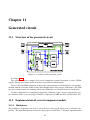
11 Generated circuit
28
11.1 Structure of the generated circuit . . . . . . . . . . . . . . . . . . . . . . . . . . . .
28
11.2 Implementation of several component models . . . . . . . . . . . . . . . . . . . . .
28
11.2.1 Multiplexer . . . . . . . . . . . . . . . . . . . . . . . . . . . . . . . . . . .
28
11.2.2 Multi-port memory . . . . . . . . . . . . . . . . . . . . . . . . . . . . . . .
29
11.2.3 FSM . . . . . . . . . . . . . . . . . . . . . . . . . . . . . . . . . . . . . .
29
11.3 VHDL style . . . . . . . . . . . . . . . . . . . . . . . . . . . . . . . . . . . . . . .
31
12 Using several components built from C
33
12.1 Commands . . . . . . . . . . . . . . . . . . . . . . . . . . . . . . . . . . . . . . .
33
12.2 Design example . . . . . . . . . . . . . . . . . . . . . . . . . . . . . . . . . . . . .
34
13 Testbench generation
36
CONTENTS
3
14 Plugins
38
14.1 The plugin xilinx . . . . . . . . . . . . . . . . . . . . . . . . . . . . . . . . . .
38
DISCLAIMER
AUGH is free software, distributed under the terms of the GNU General Public License as published
by the Free Software Foundation, version 3.
AUGH is distributed in the hope that it will be useful, but WITHOUT ANY WARRANTY; without even the implied warranty of MERCHANTABILITY or FITNESS FOR A PARTICULAR PURPOSE. See the GNU General Public License for more details.
You should have received a copy of the GNU General Public License along with AUGH. If not,
see http://www.gnu.org/licenses/.
i
Chapter 1
The AUGH purposes
AUGH stands for Autonomous and User-Guided High-level synthesis.
High-Level Synthesis (HLS) is a development flow for FPGA/ASIC meant to use relatively highlevel languages (C/C++/SystemC, Matlab, ...) instead of the traditional RTL ones (VHDL, Verilog).
The objectives of HLS are multiple:
• Accelerate development: RTL languages are too precise for many application fields. The compactness and expressivity of high-level languages accelerates development.
• Code reuse: the input description present low dependency to the hardware target. This eases
creation of hardware accelerators from a working software version.
• Coherence with simulation: the input description used for synthesis can often be compiled and
executed on a PC to obtain reference test vectors.
AUGH is a high-level synthesis tool designed for automatic generation of hardware accelerators
for FPGA, under resource and frequency constraints. It generates a generic VHDL description from
an input application written in C language.
The purpose of AUGH it to make FPGA technologies more attractive as hardware accelerator
execution devices. AUGH can be used in a very similar way to compilers, by people with low or no
expertise in digital circuit design.
Most relevant features
•
•
•
•
•
•
•
•
•
•
•
•
•
•
Input language is plain ANSI-C (see restrictions in Chapter 9).
Output is generic synthesizable VHDL. Any logic synthesis tool can accept it.
Automatic and very fast design space exploration (DSE) under resource constraints.
Embedded command interpreter. Everything can be scripted, all design transformations can be
triggered manually.
Evaluation of the design execution time even with branch conditions.
Testbench generation for RTL simulation.
Handling of resource constraints, given as raw number of LUT, FF, DSP, BRAM.
Handling of a frequency constraint.
Several optimization levels.
Automatic constant and copy propagation, common sub-expression elimination (CSE), dead
code elimination.
Operator sharing and chaining.
Operator shrinking to actual usage.
Embedded calibration for several FPGA technologies and speed grades (currently Xilinx Virtex5, speed grade 1, and Virtex-7, speed grades 1, 2, 3).
Embedded references of FPGA chips, with available resources, speed grades and packages.
1
CHAPTER 1. THE AUGH PURPOSES
2
• Embedded references of FPGA boards, with description of clock and reset sources, serial interfaces, GPIO stuff (leds, buttons, rotary encoder).
• Transparent control of vendor-specific back-end generation tools (logic synthesis, place and
route, bitstream generation, programming of the FPGA).
• Vendor-agnostic. The AUGH core can handle any FPGA technology (provided an appropriate
calibration exists, possibly in the form of a plugin).
• Extensibility with plugins. This enables to declare additional FPGA technologies, boards, communication interfaces, special “black box” components, etc.
• Retiming. The VHDL designs can be generated with special instrumentation allowing postplace-and-route FSM correction to ensure the design works at a given frequency.
Work in progress
• Handling of memory resources: Currently BRAM resources are not handled. AUGH assumes
all memory components are implemented as LUTRAM, and that all LUT can be used as LUTRAM. It means the designs can be non-synthesizable if too much memory is involved. Avoid
C descriptions with very large arrays.
• Pipelined components are not yet handled. It means multipliers are always combinatorial even
if implemented with DSP cores. Also, only asynchronous read is available on memory components. This is why BRAM primitives are not handled yet.
• Design pipelining is not yet handled.
Chapter 2
Generation flow
2.1
Toolchain integration
Figure 2.1: Integration of AUGH with the back-end tools
The Figure 2.1 illustrates how AUGH integrates in the toolchain.
As AUGH generates the project files for the back-end synthesis and place-and-route tools, it is the
only tool the user needs to interact with.
Manual modification of these files and manually launching these back-end steps is of course still
possible (e.g. for development or any other specific purpose).
2.2
AUGH generation flow
The Figure 2.2 represents the AUGH generation flow. From the input description, AUGH infers
the data interfaces (or follows what is declared for a target FPGA board) and the needed computing
operators. Usual simplifications are performed, the instructions of the input description are scheduled
and mapped onto the operators.
The allocation step consists in creating the main hardware components of the circuit (adders,
multipliers, registers, memory banks...). AUGH finds the minimal set of component needed. The
allocation extended by the design space exploration process.
3
CHAPTER 2. GENERATION FLOW
4
Figure 2.2: AUGH generation flow
The scheduling step consists in packing as many instructions as possible in the design control steps
(FSM states). This is performed with respects to data dependencies and to the number of hardware
components defined by allocation. This step gives rapidity to the circuit.
The mapping step consists in assigning a hardware component to each instruction/operation the
circuit has to execute. This step also creates all needed multiplexers and the FSM. Only then the
design size can be evaluated and presented to the user.
The frequency constraint is handled at mapping time. If a control step has a delay longer than
the clock period, the corresponding FSM state is set to last more than one clock cycle. The resource
constraint is handled by the design space exploration process (see Chapter 5).
Without DSE, the generation flow is very fast (from 10 ms to a few seconds). In scripted mode,
the user also has full possibility to transform the design (see Chapter 4),
Chapter 3
Command-line parameters
3.1
General invocation
General syntax:
augh <options> <cfile>
AUGH accepts only one input C file. It can be given as the last command-line parameter, or
specified with the command -load in case the order of the command-line parameters is relevant.
The FPGA technologies are not automatically loaded. They are usually defined as plugins. To use
an FPGA technology, the user must load the corresponding plugin with the command-line parameter
-p <name> before specifying a target board or chip.
–version Display AUGH version information. AUGH immediately exits with return code zero.
–help, -h, -u Display help about launch syntax and command-line parameters. AUGH immediately
exits with return code zero.
-load <filename> Specify the input C file. Useful for when the order in which the command-line
parameters is relevant (e.g. when using parameters -ex.
When not using -load, the input C file is the last command-line parameter, and as such it is
processed only after all other parameters.
-p, -plugin <name> Load a plugin.
The name can be an absolute path. The name of the plugin library must be complete. Example:
/foo/bar/libmyplugin.so
The name can be an path relative to the user home directory. The leading character’˜’ is replaced
by the content of the environment variable $HOME,which must be set. The name of the plugin library
must be complete. Example:
~/foo/bar/libmyplugin.so
The name can be the name of the library file. AUGH searches this file in its standard plugin
directories. Example:
libmyplugin.so
The name can be the bare plugin name. In this case, AUGH expands it (prepend "lib" and append
".so") and searches the corresponding library file in its standard plugin directories. Example:
myplugin
5
CHAPTER 3. COMMAND-LINE PARAMETERS
6
-ex <command> Execute a command using the internal command interpreter (see Chapter 6).
If the command interpreter returns non-zero (an error occurred), AUGH immediately exits with
the same error code.
If no error occurred, AUGH continues normal execution and parsing of command-line parameters.
-source <filename> Execute commands from the specified file, using the internal command interpreter (see Chapter 6).
If the command interpreter returns non-zero (an error occurred) for any command, AUGH immediately exits with the same error code.
If no error occurred, AUGH continues normal execution and parsing of command-line parameters.
-I<path>, -D<stuff> Same usage than in GCC or Clang.
-I adds a path to search include headers.
-D defines a macro.
-O0, -O1, -O2, -O3 Optimization levels.
With -O0, AUGH does only transcription to VHDL. There is not even scheduling. Only one
instruction of the input design is executed per control step (FSM state). This optimization level is
mostly useful for debug.
With -O1, AUGH performs simple assignment propagation, temporary variable elimination, instruction width optimization, and scheduling.
With -O2, AUGH performs fast design space exploration.
With -O3, AUGH performs precise design space exploration and uses more powerful simplification routines.
-script <filename> Script mode.
After parsing the command-line parameters, the specified script will be executed by the AUGH
command interpreter (see Chapter 6).
If an error occurs during the script execution, AUGH immediately returns the command interpreter
error code. Otherwise AUGH return zero.
-i
Interactive mode.
After parsing the command-line parameters, AUGH will launch the command interpreter in manual mode (see Chapter 6).
-cflags <flags> Flags for the C preprocessor and parser. Overrides any previous settings given with
-cflags, -cflags+, -cflags-add.
-cflags+, -cflags-add <flags> Add flags for the C preprocessor and parser.
-vhdl-dir <dirname> Directory where VHDL files are saved.
It can be an absolute or relative path. Default is: vhdl
CHAPTER 3. COMMAND-LINE PARAMETERS
7
-vhdl-prefix <prefix> Add the specified prefix to all names of generated VHDL entities.
-no-vhdl Skip generation of the VHDL files.
-no-synth-prj Skip generation of the back-end synthesis project files.
-c Don’t launch back-end synthesis.
-board <board-name> Select an FPGA board to do synthesis on.
If there is only one FPGA on the board, it is automatically selected, and the synthesis target is
configured for its speed grade, resources, and board connectivity.
-board-fpga <board-name> <fpga-name> Select a particular FPGA on a possibly multi-FPGA
board.
The synthesis target is configured for its speed grade, resources, and board connectivity.
-board-clock <clock-name> Select a clock source for the selected board.
Only clock sources identified in the board configuration for the selected FPGA can be selected.
The synthesis target is configured for the selected clock frequency.
-techno <name> Manually select an FPGA technology.
-chip <name> Manually select and FPGA chip to do synthesis on.
The synthesis target is configured with the corresponding technology and hardware resources. The
first speed grade available is automatically selected.
By default, if no resource constraint is manually set, AUGH resource target is 80% of the FPGA
capacity.
-speed <name> Manually select the speed grade.
Only speed grades available for a previously selected FPGA technology are accepted. This command overrides any previously selected speed grade,
A speed grade normally not available for the given FPGA chip can also be selected.
-pkg <name> Specify an FPGA package.
This is only handled by technology-specific code to generate project files for back-end logic synthesis, place-and-route and bitstream generation.
-chip-ratio <val> Set the ratio of the chip resources to use.
The value can be a floating-point number in the range 0 to 1, or a value in percent.
Example: 85%
CHAPTER 3. COMMAND-LINE PARAMETERS
8
-hwlim <string> Set resource utilization limits for each FPGA primitive.
Example: lut6:1000/dff:500
-freq <value> Set the target frequency.
Example: 100M
-reset-level <value> Set the active reset level: 0 or 1 (default).
-entity <name> Set the name of the generated top-level VHDL entity.
Default: top
-no-start Don’t add a wait-on-start loop after circuit reset.
By default, a dedicated one-wire input port is added to the top-level entity. The circuit waits for
the value ’1’ to begin computing.
info <topic> Display information about embedded data and calibration. After, AUGH immediately
exits with error code zero.
Available topics:
technos: Display all available technologies.
technos-data: Display all available technologies, with all details.
techno <name>: Display details for one technology.
chips: Display all available chips.
chips-data: Display all available chips, with all details.
chip <name>: Display details for one chip.
3.2
Invocation examples
Synthesis for a given FPGA board:
augh -p xilinx -board xupv5 app.c
Synthesis for a manually-specified synthesis target:
augh -p xilinx -techno virtex-5 -speed 1 -hwlim lut6:10000/ff:5000
-freq 125M app.c
Synthesis for a certain partition of an FPGA:
augh -p xilinx -chip xc5vlx110t -chip-ratio 18% -freq 125M app.c
Chapter 4
Design transformations
4.1
Unrolling FOR loops
The loop unroll transformation is considered when the number of iterations of a loop is statically
known. In this situation, it may be possible to execute all iterations at the same time, or to make
execution of the loop iterations overlap.
Figure 4.1: Unrolling a loop
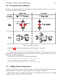
The Figure 4.1 illustrates the transformation of the design execution flow, for the following loop:
myloop1:
for(i=0; i<4; i++) { <body> }
The loop body is duplicated as many times as there are iterations in the loop. In each body
duplicate, all references to the iterator variable i are replaced by the corresponding iterator value.
The body duplicates are simply appended to each other. This ensures data dependencies between
iterations (if any) are respected. The result is a new, large, basic block. Later, the scheduler will take
care of the new parallelism opportunities.
To manually unroll a loop, use the following command:
hier node-loop find label myloop1 unroll-seq full
Partial unroll is also available with the following command:
hier node-loop find label myloop1 unroll-part 4
The DSE process only handles full unroll. It also only handles loops whose body is only a basic
block.
It is also possible to find loops from a source line:
hier node-loop find line 79 unroll-seq full
9
CHAPTER 4. DESIGN TRANSFORMATIONS
4.2
10
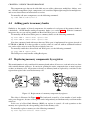
Wiring branch conditions
By default, conditional assignments as described in C language with the keywords if and switch
are implemented with a branch condition.
Figure 4.2: Wiring a condition
The Figure 4.2 illustrates the transformation of the following if construct:
myif1:
if(A + B == 0) R = C + D; else R = E + F;
A conditional jump is replaced by an unconditional assignment. This assignment can then be
merged with the other instructions that were before and after the if construct, which can offer very
interesting scheduling optimizations.
To manually wire a condition, use the following command:
hier node-switch find label myif1 one-cycle
It is also possible to find a condition from a source line:
hier node-switch find line 99 wire one-cycle
4.3
Adding shared components
A fast design is one that executes a lot of instructions at a time. By default, AUGH allocates only the
minimum number of components to map the instructions of the input C description.
But this allows only a low number of instructions to be scheduled a given control step. Adding
components to the circuit can reduce this bottleneck.
CHAPTER 4. DESIGN TRANSFORMATIONS
11
The component types that can be added this way are adders, subtractors, multipliers, shifters, rotators. All other components (logic, comparators) are considered lightweight compared to multiplexers,
and are not shared between instructions to execute.
To manually add some components, use the following command:
op add add:8/sub:8/mul:6
4.4
Adding ports to memory banks
Similarly to the number of shared components, the number of read ports of the memory banks is
a bottleneck. AUGH handles multi-port memory banks (see section 11.2.2). With the command
interpreter, the user can add any number of Read and Write ports as desired.
To manually add Read and Write ports to a memory bank, use the following commands:
op mem-add-r <mem-name> <ports-nb>
op mem-add-w <mem-name> <ports-nb>
Note that a memory bank with more than one Write port is implemented in registers instead of
LUTRAM or BRAM. It is then possible to read the value of each cell with no additional hardware
cost, and to add a write to each cell with a relatively low cost.
To manually enable these direct Read and Write ports, use the following command:
op mem-add-d <mem-name>
The DSE process only handles adding Read ports.
4.5
Replacing memory components by registers
This transformation is only considered for memory banks where all accesses (read and write) are done
with statically-known addresses. It consists in splitting the entire component into as many registers
as there are memory cells. All previous references to memory bank are replaced by a reference to the
register that replaces the associated memory cell.
Figure 4.3: Replacement of a memory component by registers
The effect is illustrated in Figure 4.3. The bottleneck created by a low number of read and/or
write ports disappears, because each register can be independently an simultaneously read from and/or
written to.
In the case of a Read-Only Memory (ROM), no register is created: all read operations to the
memory are replaced by the corresponding value in the memory cells.
To manually replace a memory, use the following command:
op mem-replace-direct <mem-name>
Chapter 5
Design space exploration
5.1
Exploration algorithm
The principle of the DSE algorithm in AUGH is the following. First, an initial low-area solution is
generated. This is obtained with maximum operator sharing. If this initial solution does not respect
resource constraints, the process is aborted and AUGH considers there is no solution.
If the initial solution is valid, the process enters the main exploration loop. Iteratively, transformations are applied to the design in order to take advantage of parallelism opportunities (the list of
transformation types is given in Chapter 4). The transformations applied are those that bring highest
design speedup, while having the lowest cost in hardware resources.
This process will tend to increase hardware resource usage of the design. The end of the exploration process is reached when the design cannot be made faster without going beyond the resource
constraint. The final solution, the one kept by AUGH, is the last obtained one that respected the
resource constraints.
Figure 5.1: Progression of the DSE
The Figure 5.1 illustrates the progression of the exploration process.
The exploration of the solutions is not exhaustive, hence the final solution may not be a theoretically optimal solution for the given constraint. It simply is the best that can be reached, in a reasonable
time, by the heuristics internally used by AUGH.
12
CHAPTER 5. DESIGN SPACE EXPLORATION
13
Figure 5.2: Selection of transformations
5.2
Selection of transformations
The Figure 5.2 illustrates how the transformations are selected. At each iteration of the exploration
loop, AUGH detects the feasible transformations. For each one, AUGH estimates the design speedup
this transformation can bring, and the cost in hardware resources.
For this purpose, each transformation type is associated to a set of estimators. This enables to
trade precision for DSE rapidity.
Also, AUGH has the possibility to select and apply more than one transformation per DSE iteration.In this mode, AUGH selects transformation that are relatively independent from each other. The
estimated speedup and resource cost of the set of transformations can then be taken as the sum of the
contributions of each individual transformation.
AUGH also has an alternative to estimators: for a given transformation, or a set of transformations,
AUGH can actually apply them on a copy of the internal representation of the design. This process is
much slower but also much more precise.
By default, AUGH can apply several transformations per iteration, and it uses estimations.
To force AUGH to apply only one transformation per iteration, use this command:
core elabo-fd-max 1
To force AUGH to use precise weighting instead of estimations, use this command:
core fd-weight-exact
5.3
DSE timeout
Specific commands are available to limit the DSE time.
To force AUGH to perform at most <N> iterations, use this command:
core elabo-iter-max <N>
A DSE timeout can also be set. This is checked at the beginning of each iteration. Use this
command (default unit is second):
core elabo-timeout <string>
Examples of syntax for <string>:
10
1m30s
1h
CHAPTER 5. DESIGN SPACE EXPLORATION
5.4
14
Generation of traces
The DSE process can generate execution traces for later analysis and plotting. The data is written in
a text file.
The first line begins by the character ’#’ and is a comment. It gives the title of each data column.
Then, for each explored solution, one line of data is added to the file. The values are separated by
space characters. There is the following pieces of information:
•
•
•
•
the solution index (0 means the initial solution),
the resource consumption, for each available primitive of the GPGA (LUT, FF, DSP, ...),
the estimated average execution time of the circuit (unit is clock cycles),
the execution time of AUGH since the beginning of the DSE process (unit is second).
This is not enabled by default. To enable export of DSE traces, use the following command:
core graph-file open elaboration-data.txt
Chapter 6
Command interpreter
AUGH features an embedded command interpreter. It allows to set parameters, examine the internal
design representations (instruction graph, netlist), apply transformation, launch generation processes,
etc.
6.1
General
The command interpreter is a custom ultra-lightweight implementation. It has a hierarchical structure:
there are sub- command interpreters that globally correspond to the main modules AUGH consists of.
A command consists of a string where at least the first word is a recognized command. This first
word is extracted from the string, and the corresponding process is launched, with the rest of the string
as parameters (it may be empty).
The command help, also widely handled in sub- command interpreters, will display the available
commands with a short syntax description.
If the first word is the name of a sub- command interpreter, the rest of the string is transmitted to
the corresponding interpreter process. The sub-interpreter then extracts the first command, and so on.
Comments are handled. The character ’#’, placed at the beginning of a command string or after
any space character, means that the rest of the line is a comment.
Warning: don’t use the characters ’"’ and ’’’ as string delimiters. AUGH does not handle that,
and has no use for that anyway. If a pair of those is used around an identifier, they are assumed to be
part of it.
6.2
Error handling
The command interpreter returns an integer. The value zero means no error, otherwise it is handled
as an error code.
When executing commands from a script file, any encountered error causes abortion of the execution of the script. To ignore potential errors on a non-critical command, launch it with the command
noerr.
15
CHAPTER 6. COMMAND INTERPRETER
6.3
6.3.1
16
Special-purpose command interpreters
Plugins
Each plugin can declare its own command interpreter. To send a command to it, use the following
syntax:
plugin cmd <plugin-name> <command>
To send multiple commands to a plugin, each of them must be sent the way above.
6.3.2
Technology library
The technology library can declare a special command interpreter. This is useful to set vendor-specific
parameters.
This command interpreter can be accessed the following way:
techno cmd <command>
Example:
techno cmd keep-hier yes
6.4
6.4.1
Examples of scripts
Simple design transcription to VHDL
# All executed commands will be printed in the terminal
commands-disp
# Load the plugin for Xilinx techno
plugin load xilinx
# Load the input C description
load app.c
# Initial simplifications
hier upd
# Select the target
techno set-board xupv5
# Display some miscellaneous data
hier time disp
hier clockcycles
# Perform mapping
postprocess
# Evaluation of design size
techno eval
CHAPTER 6. COMMAND INTERPRETER
17
# Generation of VHDL
vhdl
# If needed, a testbench can be generated
# (uncomment the following lines, put them on a single line)
#netlist tb-gen -odir vhdl -cy 2000 -rawbin
# -the-in -f invectors.bin -the-out -f outvectors.bin
# Generate the project files for back-end logic synthesis etc
backend-gen-prj
# Launch back-end logic synthesis etc
backend-launch
# Information about system resources AUGH used (memory and running time)
augh-resource
Chapter 7
Hardware target specification
The specification of a hardware target consists of 4 pieces of information:
•
•
•
•
the FPGA technology (e.g. virtex-5 or virtex-7),
the speed grade,
the hardware resources, given as bare FPGA primitives (e.g. LUT„ FF, DSP...),
the target frequency.
There are several possible ways to give the pieces of information to AUGH. It is possible to set
them manually for a full custom target, or the user can use shortcuts by specifying a target FPGA chip
reference or a target FPGA board.
It is also possible to mix custom specification and selection of an FPGA chip or an FPGA board.
The specifications given last overrides previous specifications.
7.1
Custom settings
Example of command-line parameters:
-techno virtex-7 -speed 3 -hwlim lut6:1000/dff:500 -freq 100M
Corresponding commands for the command interpreter:
techno set-techno virtex-7
techno set-speed 3
hwlim lut6:1000/dff:500
target-freq 100M
7.2
FPGA chips
AUGH embeds descriptions for all FPGA chips for the technologies Xilinx Virtex-5 and Virtex-7.
By specifying an FPGA chip reference, AUGH automatically selects the corresponding technology, one arbitrary speed grade available for the chip, and the corresponding hardware resources. By
default, AUGH targets 80% of the FPGA.
Example of command-line parameters:
-chip xc7v585t -speed 3 -freq 100M
Corresponding commands for the command interpreter:
18
CHAPTER 7. HARDWARE TARGET SPECIFICATION
19
techno set-chip xc7v585t
techno set-speed 3
target-freq 100M
7.3
FPGA boards
AUGH handles FPGA boards as synthesis target. Multi-FPGA boards are handled. For each FPGA
present, the board description includes:
• the FPGA reference (with speed grade, hardware resources and package),
• the position in the JTAG chain if applicable,
• the available connectivity.
The description of the available connectivity can include:
•
•
•
•
•
the clock sources (with frequency),
the reset sources (with active state),
the UART interfaces (with recommended baudrate value and parity handling),
the rotary encoders,
the general purpose inputs and outputs (for LEDs, buttons...).
Currently board descriptions are declared with plugins. Descriptions of custom boards can be
handled with custom plugins.
Currently the plugin "xilinx" declares the description of the board XUPV5.
Example of command-line parameters to target a board:
-board xupv5
Corresponding commands for the command interpreter:
techno set-board xupv5
Chapter 8
Top-level interfaces
The top-level ports and communication interfaces is assumed to be set by the user. This can correspond to connectivity available on an FPGA board, or an interface specific to a NoC. For this reason,
AUGH will not try to transform the data interfaces.
8.1
Basic input and output ports
Currently only handled when targeting an FPGA board. The description of the board interfaces contains input and output ports. In the input design, AUGH searches the variables whose name correspond to a port declared in the board interfaces.
When a match is found, AUGH creates a top-level port and all references to the variable are
replaced to references to the port.
A port declared as input can’t be written to. AUGH inserts a buffer for output ports. These ports
can then be written to and read from.
8.2
FIFO
A FIFO interface is a set of 3 ports: data, rdy, and ack.
The port data can be of any width, up to 128 bits. If the FIFO direction is output, then the port
is an output port, otherwise it is an input port.
The ports rdy and ack are both 1-bit ports. rdy is always an output port, and ack is always an
input port.
When the component is ready to perform a data transfer (input or output), it sets its port rdy to
’1’, and waits for the value ’1’ on its port ack.
The transfer happens at a rising-edge clock front, when both rdy and ack are at ’1’. It means
both the sender and the receiver declared themselves as ready (they set their port rdy at ’1’), and
each was aware the other was ready (each port rdy is connected to the port ack othe the other).
Currently the FIFO does not contain a circular buffer (it is a separate component). So the current
behaviour is more a GALS interface than a FIFO component.
8.3
UART
FIXME TODO
20
CHAPTER 8. TOP-LEVEL INTERFACES
8.4
Data buffers
FIXME TODO: circular buffer, ping-pong
8.5
Clock divider
FIXME TODO
21
Chapter 9
Accepted input C descriptions
Note: AUGH has some limits to its parsing capabilities. Most are inherited from the UGH tool parser,
which was based on GCC version 2.8.1.
9.1
Accepted subset of C
Full ANSI C support is assumed except about the following points.
•
•
•
•
•
•
The top-level function must be of this form: void augh_main();
No arrays in structures and unions.
No enumerated types.
Only divisions of unsigned values by powers of 2 are handled.
No function recursion.
Functions may return void or a scalar. In particular, returning structures or unions is not handled. Similarly, function arguments can only be scalars (or pointers in specific circumstances).
• No pointer arithmetic. Some pointers may be used as arguments of inline functions but should
be avoided as this has some undocumented limits. Instead, prefer global variables or macros.
• No floating-point.
• No function calls nor variable assignments in return statements and inside tests with if,
switch, the ’?:’ ternary operator, and exit tests in loops.
Additional notes:
• Functions declared static inline are instantiated at all call locations (i.e. the function
body is duplicated). Other functions are not, except when they are called from only one location.
• Some coding styles may lead to wrong estimations of the design execution time, especially
about usage of keywords goto, continue, break and return. See Chapter 10, page 26.
9.2
Default parser options
AUGH adds the option -Wall. As usual this enables display of all parsing warnings.
9.3
Built-in macro definitions
The AUGH parser defines the preprocessor macro AUGH_SYNTHESIS.
22
CHAPTER 9. ACCEPTED INPUT C DESCRIPTIONS
23
The C code of the applications can check whether this macro is defined to select an implementation
optimized for synthesis with AUGH or optimized for any other synthesis or compilation tool.
Example:
#ifdef AUGH_SYNTHESIS
// Implementation for AUGH
#else
// Implementation for other tools
#endif
9.4
Built-in data types
All variable types int1_t, int2_t up to int128_t, and the unsigned variant uint1_t up to
uint128_t, are internally recognized by AUGH. The literal indicates the bit width (like a superset
of the C99 standard integer types).
The bool type is defined as uint1_t. Similarly to C99, true and false are defined respectively as 1 and 0.
9.5
Include headers
Directives to include local headers (example: #include "myheader.h") are properly handled.
Directives to include system headers (example: #include <sysheader.h>) only handle
headers shipped with AUGH.
The available system headers are:
• augh.h
Declaration of builtin functions for access to FIFO channels, sleep functions, etc (see section 9.6, page 23).
• augh_annot.h
Declaration of variables that AUGH uses to recognize user annotations (see Chapter 10, page 26).
• augh_types.h
AUGH-specific type definitions for unusual bit width variables (see section 9.4, page 23).
• And some headers specific to FPGA boards declared by plugins.
9.6
Built-in functions
Warning: currently there is no guarantee built-in functions are parsed and replaced in the order they
appear in the C program.
9.6.1
Built-in functions related to top-level ports
Create top-level ports from declared variables. The bit width of the ports is identical to the width of
the declared variables.
• void augh_port_in(int var)
Replace the register var by a top-level input port. It mut not be written to in the program.
CHAPTER 9. ACCEPTED INPUT C DESCRIPTIONS
24
• void augh_port_out(int var)
Create a new top-level output port connected to the register var. The register is kept and can
still be read from and written to.
9.6.2
Built-in functions related to FIFO interfaces
Creation of FIFO interfaces Create top-level FIFO interfaces from declared variables. The data
bit width of the FIFO is identical to the width of the declared variables.
• void augh_access_fifo_in(int var)
Replace the register var by a top-level FIFO input interface. It mut not be written to in the
program.
• void augh_access_fifo_out(int var)
Replace the register var by a top-level FIFO output interface. It mut not be read from in the
program.
Blocking operations
• void augh_read(int fifo, void* data)
Create a waiting loop for FIFO handshaking. A value is read from the fifo channel, sign extended if the first operand is signed.
• void augh_write(int fifo, void* data)
Create a waiting loop for FIFO handshaking. A value is sent to the fifo channel, sign extended
if the second operand is signed.
• void augh_read_vector(int fifo, void* data, unsigned nb)
Read several values from a FIFO channel. Behaves like:
for(int i=0; i<nb; i++) augh_read(fifo, &data[i]);
• void augh_write_vector(int fifo, void* data, unsigned nb)
Writes several values to a FIFO channel. Behaves like:
for(int i=0; i<nb; i++) augh_write(fifo, &data[i]);
Non-blocking operations
•
•
•
•
•
•
•
•
•
•
9.6.3
bool
bool
void
void
void
void
void
void
bool
bool
augh_tryread(int fifo, void* data)
augh_trywrite(int fifo, void* data)
aughin_setready(int fifo)
aughout_setready(int fifo)
aughin_setreadyval(int fifo, bool val)
aughout_setreadyval(int fifo, bool val)
aughin_spydata(int fifo, void* data)
aughout_setdata(int fifo, void* data)
aughin_spyready(int fifo)
aughout_spyready(int fifo)
Built-in functions related to UART interfaces
Create UART Rx and UART Tx top-level interfaces, and the associated FIFO-UART interface components, from declared variables.
The data bit width of the FIFO interface of the created components is identical to the width of the
declared variables.
CHAPTER 9. ACCEPTED INPUT C DESCRIPTIONS
25
• void augh_access_uart_rx(int var)
Create a top-level UART Rx interface, create a FIFO-UART interface component, remove the
register var, and replace all operations on var by operations on the output FIFO interface of
the created component.
• void augh_access_uart_tx(int var)
Create a top-level UART Tx interface, create a UART-FIFO interface component, remove the
register var, and replace all operations on var by operations on the input FIFO interface of
the created component.
9.6.4
Built-in functions related to wait loops
• sleep(unsigned nb)
Wait for at least nb seconds.
• usleep(unsigned nb)
Wait for at least nb microseconds.
• nsleep(unsigned nb)
Wait for at least nb nanoseconds.
• cysleep(unsigned nb)
Wait for at least nb clock cycles.
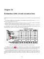
Chapter 10
Estimation of the circuit execution time
AUGH can estimate the execution time of the generated circuit, even if there is data-dependent control
flow.
By default, AUGH assumes all branches of each conditional node (the C keywords if, switch)
have the same probability to be taken.
When AUGH can infer the number of iteration of a loop (a for loop for example), this number
is taken into account. Otherwise the loop is assumed to iterate only once.
The user can override this behaviour by adding annotations to the C input description. Annotations
are assignments to special variables. They specify the branch probability of the branches of the
conditional nodes, and the average number of iterations of the loops.
Figure 10.1: Estimation of the circuit execution time, with annotations
As illustrated in Figure 10.1, these annotations do reveal where are the actual hot spots in the
input description. The relative criticality of each basic block is then correctly handled, which makes
AUGH able to apply design transformations where most relevant for the circuit execution time.
Note that AUGH always displays 3 values for the circuit execution time (in clock cycles): the
minimum, maximum, and the value according to annotations. However, for loops whose number of
iteration is unknown and where no annotation was specified, AUGH still assumes they iterate only
once.
26
CHAPTER 10. ESTIMATION OF THE CIRCUIT EXECUTION TIME
27
The variables used for annotations are declared by including the following header in the input
description:
#include <augh_annot.h>
10.1
Annotations: loop iterations
To indicate that a certain loop iterates on average N times, add the following assignment at the beginning of the loop body:
augh_iter_nb = N;
Note that N must be integer. When a floating-point value is needed, indicate a value multiplied by
1000 with the following annotation:
augh_iter_nb_m = Nm;
In case the user knows that the number of iterations will always be a multiple (>0) of a power of
2, is is possible to partially unroll the loop. To enable that in AUGH, use the following annotation:
augh_iter_nb_power2 = factor;
10.2
Annotations: branch probabilities
To indicate a certain branch is taken with an average branch probability prob (in percent), add the
following assignment at the beginning of the branch body:
augh_branch_prob = prob;
Note that prob must be integer. When a floating-point value is needed, indicate a value in per1000 with the following annotation:
augh_branch_prob_m = probm;
For even more precision, indicate a value in per-1000000 with the following annotation:
augh_branch_prob_u = probu;
10.3
Coding styles to avoid for correct estimation
Some coding styles prevent proper estimation of the circuit execution time. AUGH will run like usual
but execution time estimation can be very wrong and design space exploration can lead to strongly
sub-optimal designs.
Basically, these are coding styles that break code hierarchy:
•
•
•
•
•
usage of goto,
usage of continue and break in loops,
usage of break not at the end of case bodies of switch constructs,
usage of return not at the end of a function body,
usage of functions called from different places, when the behaviour of the function body varies
notably depending on the origin of the call.
Chapter 11
Generated circuit
11.1
Structure of the generated circuit
Figure 11.1: structure of the generated circuit
See Figure 11.1
The generated circuit is composed of several components connected together by wires (VHDL
signals). The top-level entity model itself does not contain any functionality.
There is only one FSM component. It drives the selection inputs of all multiplexers, the synchronization with the rest of the world, and the Write Enable inputs of the storage components. The FSM
may also contain features for retiming (when some FSM states can last more than one clock cycle).
All other components are computing components (arithmetic, logic), storage components (registers, memory banks), or special-purpose interface components (UART interface, circular buffer, etc).
11.2
Implementation of several component models
11.2.1
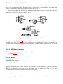
Multiplexer
The multiplexer components are used to select the data source of the input ports of all other components. The implementation best suited for this purpose in AUGH is a "decoded" implementation
28
CHAPTER 11. GENERATED CIRCUIT
29
(contrary to binary-encoded multiplexer). In this implementation, for a multiplexer N to 1 there
are N 1-bit selection inputs. Each data input source is associated to a selection signal, and a data input
source is selected when the corresponding selection signal is at ’1’.
The selection signals are driven by the FSM. The FSM ensures that at any given time, for each
multiplexer, at most one selection signal is at ’1’.
Figure 11.2: Implementation of a decoded MUX
As illustrated in Figure 11.2, this implementation can be very efficiently packed into the LUT of
an FPGA. It is also well adapted to set a default input or a default value when no input source is
selected, and it lets the possibility for the back-end logic synthesis tool to optimize delay for certain
input sources.
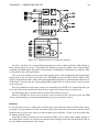
11.2.2
Multi-port memory
FIXME TODO: implem as mem, as registers + MUX, etc
See Figure 11.3
11.2.3
FSM
FIXME TODO: A figure?
Implementation one-hot
The FSM implementation style is "one-hot". It means that, for an FSM with N possible states, the
FSM has a N-bits state register and, at any given time, only one of these bits is at ’1’. So each
possible state is associated to a unique bit of this state register.
Buffering of outputs
Due to possibly high datapath delay, some states may need more than one clock cycle to terminate.
CHAPTER 11. GENERATED CIRCUIT
30
Figure 11.3: Implementation of a multi-port memory
In such a situation, the corresponding datapath routes must remain perfectly stable during as
many clock cycles as necessary. To guarantee the FSM won’t generate glitches due to internal logic
switching, the FSM outputs that drive selection inputs of multiplexer components are buffered. This
is also good for the critical path delay.
Also, in case of a multi-cycle state, the actual storage of the results computed by the datapath must
happen only at the last clock cycle of the state. The FSM generates the Write Enable inputs of the
registers and memory banks, along with some handshaking signals for synchronization with the rest
of the world. It means that the corresponding FSM outputs must be activated only at the last clock
cycle of the state.
For deep technical reasons, these outputs are not buffered in AUGH. It is assumed that they are
not on the critical path and that the delay on these signals will always fit in one clock cycle.
AUGH handles these situations with an internal delay analysis process.
However AUGH can’t foresee the actual post- place-and-route delays. For this reason, the FSM
can be generated with special instrumentation for post- place-and-route retiming.
Retiming
It’s not possible to foresee, at HLS time, what the post- place-and-route delays will look like. Often,
passing a very large number of delay constraints to the place-and-route tool (one for each bit of each
datapath route of each state) leads to an unreasonable processing time. It may even be possible that
no solution actually exists.
Generally, in such a situation, the user launches the HLS process again, with a higher margin on
the clock period. Or, the user can keep the obtained routed design, but a lower clock frequency has to
be used, which slowdowns the entire circuit.
CHAPTER 11. GENERATED CIRCUIT
31
Post- place-and-route FSM retiming is a lighter solution with a lower impact on overall circuit
speed. The place-and-route process can be launched with relatively loose constraints. Then, the delays
of the routed circuit are analyzed. When a datapaths delay exceeds was the FSM was configured for,
an appropriate correction is applied to the FSM.
For this purpose the FSM can be generated by AUGH with a special instrumentation that makes
post- place-and-route analysis and correction possible. It uses the LUT6 primitive of the VHDL
library unisim. To enable it, use the following command:
netlist fsmretime-lut6 yes
Note that AUGH itself can’t perform this retiming correction. This operation needs specific integration with dedicated vendor tools for analysis and bitstream manipulation, and this is not yet ready.
The instrumentation performed by AUGH consists of a clock cycle counter and some logic blocks
to indicate the end of each state. Each state is associated to one particular logic block.
The clock cycle counter has a width of 5 bits. It is reset at each transition.
Figure 11.4: Implementation of the retiming comparator with LUT6
The Figure 11.4 illustrates the implementation of the logic block that indicates the end of an FSM
state. The end of the state is reached when the output is at ’1’.
The logic block is designed to fit inside one LUT6. A given logic block returns ’1’ only when
the FSM state it is associated to is the current state and the clock counter value corresponds to the end
of the state.
So the duration of each FSM state can be specified by changing the corresponding LUT configuration. The available range is 1 to 32 clock cycles. This operation can be performed after place-androute with a bitstream editor.
11.3
VHDL style
The VHDL code can be generated in several VHDL styles: one for simulation speed, one for good
human readability, and one for logic synthesis speed.
The user can select the desired VHDL style with the following commands:
netlist objective-simu
netlist objective-human
netlist objective-synth
Note that this only indicates the user preference. Most component models only have one VHDL
generator, that may or may not correspond to the mentioned styles.
These VHDL styles are mostly useful for complex components, for debug or manual instrumentation purposes. The FSM generator handles these styles.
Also, by default, one VHDL file is created per component instance. When generating large circuits, there can be a lot of them. To limit the number of created components, the VHDL code of many
CHAPTER 11. GENERATED CIRCUIT
32
component models can be inserted inside the top-level component body. This is enabled by default.
To disable it, use the following command:
netlist comps-inline no
Chapter 12
Using several components built from C
C source files can be loaded as custom hardware components models. In AUGH, these custom component models are called "implementation models".
These component models can be instantiated as components in the top-level entity, and connected
together or with the top-level interfaces.
It’s important to note that:
•
•
•
•
All instances of a component model use the same implementation.
Each instance has its own FSM.
Each instance owns the operators it uses (adders, registers, etc).
There is no operator sharing between the top-level entity and the instances of component models, nor between two instances of a same component model.
• It’s not yet possible to launch design space exploration with per- component model resource
constraints (work in progress).
• It is not yet possible to build component models from other component models (work in progress).
12.1
Commands
To load the source file mycomp.c as a component model named mycomp, use the following command:
loadmod mycomp mycomp.c
To instantiate this model as components mycomp0 and mycomp1, use the following command:
build inst mycomp mycomp0 mycomp1
To connect the interface chan_in of the component mycomp1 to the top-level interface stdin,
use the following command:
build link mycomp0.chan_in stdin
This command is rather versatile. For example it can connect a top-level UART Rx interface
to an input FIFO interface of a component, transparently creating the UART component interface
component. The order the two interfaces are given in has no importance.
To apply commands on a specific component model modelname, use the following command:
impmod -m <modelname> <commands>
To apply commands on all component models, including the top-level component, use the following command:
impmod forall <commands>
33
CHAPTER 12. USING SEVERAL COMPONENTS BUILT FROM C
34
About VHDL files: as all instances share the same implementation, they refer to the same VHDL
files. These files are named after the component model name: the main entity is named mycomp and
the name of each sub-component instance is prefixed with mycomp_.
12.2
Design example
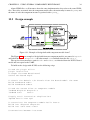
Figure 12.1: Example of design built with component models from C
The Figure 12.1 is an example of design built from two component models, one named dispatch
and built from the file dispatch.c, the other named core and built from the file core.c.
The top-level data interfaces, named stdin and stdout, are inherited from the XUPV5 board
model and correspond to the UART.
To build such a design with AUGH, use the following script:
# Load the plugin Xilinx
plugin load wilinx
# Target the FPGA board XUPV5
techno set-board xupv5
# Inherit the default I/O chanels from the board model: the UART
build fromboard stdin
build fromboard stdout
# Load the source files as component models
loadmod dispatch dispatch.c
loadmod core
core.c
# Apply usual instruction simplications
impmod forall hier upd
# Instantiate the component models built from C
build inst dispatch dispatch0
build inst core core0 core1
# Connections between instances
CHAPTER 12. USING SEVERAL COMPONENTS BUILT FROM C
build
build
build
build
link
link
link
link
dispatch0.core0_send
dispatch0.core0_recv
dispatch0.core1_send
dispatch0.core1_recv
core0.chan_in
core0.chan_out
core1.chan_in
core1.chan_out
# Top-level interfaces
# UART Rx/Tx interface components are transparently created
build link stdin dispatch0.chan_in
build link stdout dispatch0.chan_out
# Perform mapping and netlist simplifications
impmod forall postprocess
# Display the size of each component model
impmod sizes-compute
impmod sizes-print
# Generate all VHDL files
impmod forall vhdl
# Generated the synthesis project files for XST
plugin cmd xilinx gen-xst-project
35
Chapter 13
Testbench generation
For simulation purposes, AUGH can generate VHDL testbenches. Testbenches can be generated for
circuits with any kind and any number of top-level interfaces. For FIFO interfaces, test vectors can
be specified.
To generate a VHDL testbench file, use the following command:
netlist tb-gen [options]
This command creates the file tb.vhd in the default VHDL directory.
Options
• -odir <dir>
The VHDL file is created in the specified directory.
• -cy <nb>
The simulation will stop after <nb> clock cycles. Default is 10 000.
Options related to test vectors
• -name <name>
Select a top-level interface with its name.
• -the-in
Select the input FIFO. Only one input FIFO must be present.
• -the-out
Select the output FIFO. Only one output FIFO must be present.
• -f <file>
Set the file that contains test vectors to the selected interface.
The type of the files that contain the test vectors can be text or binary.
For the text file type, each vector is a number. The number format can be hexadecimal, decimal
(signed or unsigned) or binary (characters ’0’ and ’1’). They are separated by space characters,
commas or comments. A comment begins by the character ’#’ and ends at the next newline character.
By default, all values are positive. Sign characters (’+’ and ’-’) are accepted but the negation
is only taken into account for decimal values.
Options related to file types for test vectors
36
CHAPTER 13. TESTBENCH GENERATION
37
• -auto
The file is a text file. The value format is automatically detected for each vector: a hexadecimal
value begins by 0x, a binary value begins by 0b (the case does not matter), otherwise it is a
decimal value.
• -hex
The file is a text file. The value format is hexadecimal. Leading 0x optional.
• -dec
The file is a text file. The value format is decimal.
• -bin
The file is a text file. The value format is binary. Leading 0b optional.
• -rawbin
The file is a binary file. All vectors use the same number of bytes.
Options related to the binary file type
• -le
The bytes for each test vector are stored little-endian style (default).
• -be
The bytes for each test vector are stored big-endian style.
• -nb <nb>
Set the number of bytes used for each test vector. By default, it is set to the minimum number
of bytes to fit the FIFO width.
Note For the options to set the file type and the options specific to the binary file type, if used before
an interface is selected, it sets the default value for all interfaces and for the current the command line
only.
Using these options when an interface is selected makes them applied only for the selected interface.
Chapter 14
Plugins
Currently AUGH is distributed with a plugin named xilinx.
14.1
The plugin xilinx
The plugin xilinx it is a demonstration-only plugin. It contains data and functions to enable AUGH
to target the FPGA chips of the vendor Xilinx.
What it contains is:
• the list of supported technologies (Virtex-5, Virtex-7 and the Zynq family),
• the timing parameters for the supported speed grades,
• the list of supported FPGA chips with their speed grades and available resources (in LUT,
LUTRAM, FF, DSP, BRAM),
• functions that enable AUGH to estimate the size of the designs and the progation time of signals,
• functions that enable AUGH to estimate the size of the designs
• a generator of project files to launch logic synthesis, placement and routing with the software
tools Xilinx XST and Xilinx Vivado,
• a little command interpreter that plugs into AUGH’s main command interpreter and that enables
to set techno-specific parameters (disable usage of DSP blocks, keep RTL hierarchy, etc),
• a limited description of two FPGA boards: XUPV5 and Zybo.
The list of supported technologies, their speed grades and the supported FPGA chips is in a configuration file in the JSON format. This file can be manually modified to fit special purposes.
The description of the FPGA boards is currently hardcoded in the plugin source code. This description contains these pieces of information:
•
•
•
•
the references of all FPGA chips present on the board,
the hardware interfaces available to each FPGA (serial link, LED, switches, etc),
the position of each FPGA on the JTAG chain (if any),
and the name of the cable driver for the software xc3sprog.
For each board, there is also a C-language header file that declares the hardware interfaces of
the board. This enables users of AUGH to use these interfaces as easily as ports in a traditional
microcontroller.
38