1
GRLIB Interface to Hard FPGA Subsystems
A GRLIB Template Design for the Terasic SoCKit Board
Master’s Thesis in Embedded Electronic System Design
MARTIN GEORGE
Department of Computer Science & Engineering
Chalmers University of Technology
Göteborg, Sweden 2015
The Author grants to Chalmers University of Technology and University of Gothenburg the non-exclusive right to publish the Work electronically and in a non-commercial
purpose make it accessible on the Internet. The Author warrants that he/she is the
author to the Work, and warrants that the Work does not contain text, pictures or other
material that violates copyright law.
The Author shall, when transferring the rights of the Work to a third party (for example
a publisher or a company), acknowledge the third party about this agreement. If the
Author has signed a copyright agreement with a third party regarding the Work, the
Author warrants hereby that he/she has obtained any necessary permission from this
third party to let Chalmers University of Technology and University of Gothenburg store
the Work electronically and make it accessible on the Internet.
GRLIB Interface to Hard FPGA Subsystems
A GRLIB Template Design for the Terasic SoCKit Board
MARTIN GEORGE
c MARTIN GEORGE, June 2015.
Examiner: PER LARSSON-EDEFORS
Chalmers University of Technology
University of Gothenburg
Department of Computer Science and Engineering
SE-412 96 Göteborg
Sweden
Telephone + 46 (0)31-772 1000
Cover: The cover shows the Terasic SoCKit development board.
Department of Computer Science and Engineering
Göteborg, Sweden June 2015
i
Abstract
Many FPGA vendors implement hard subsystems in their FPGAs, such as the Xilinx
Zynq-7000 SoC, and the Altera Cyclone V SoC. A common trait for several SoC FPGAs
is that they have AXI interfaces in the interconnect between the hard subsystem and
the FPGA fabric. Cobham Gaisler develops and supports the VHDL IP library GRLIB,
and want to be able to interface GRLIB to such hard subsystems.
This Master of Science thesis describes the implementation of a GRLIB template design
for the Altera Cyclone V SoC FPGA, on the Terasic SoCKit board. The design demonstrates how GRLIB can be connected to a hard subsystem, in this case the Altera HPS,
using the AXI available interfaces.
The template design runs at a clock frequency 70 MHz, and includes a LEON3 processor,
as well as several other GRLIB IP cores. An existing AHB-to-AXI bridge was modified,
and a new AXI-to-AHB bridge was developed to connect the GRLIB AHB bus to the
hard subsystem AXI interfaces. The project was executed and successfully verified at
Cobham Gaisler.
Keywords: LEON3, GRLIB, FPGA, Altera, SoC, HPS, AXI, AHB, VHDL, IP-core,
HPS2FPGA, FPGA2HPS.
ii
iii
Acknowledgements
I would like to thank my supervisor at Cobham Gaisler, Jan Andersson, for all the help
and valuable feedback during the course of the project. I would also like to thank the
rest of the staff at Cobham Gaisler for their support, especially to Andrea Gianarro. He
provided invaluable help, and several problems would have taken significantly longer to
solve without him. Finally, I would also like to thank my supervisor at Chalmers, Lars
”J” Svensson, and my examiner Per Larsson-Edefors for their advice and feedback on my
report.
Martin George, Göteborg 2015
iv
v
Contents
1 Introduction
1.1 Background . . .
1.2 Purpose and Aim
1.3 Scope . . . . . .
1.4 Thesis Outline .
.
.
.
.
2 Method
2.1 Procedure . . . . .
2.1.1 Verification
2.2 Software Tools . .
2.3 Hardware Platform
.
.
.
.
.
.
.
.
.
.
.
.
.
.
.
.
.
.
.
.
.
.
.
.
.
.
.
.
.
.
.
.
.
.
.
.
.
.
.
.
.
.
.
.
.
.
.
.
.
.
.
.
.
.
.
.
.
.
.
.
.
.
.
.
.
.
.
.
.
.
.
.
.
.
.
.
.
.
.
.
.
.
.
.
.
.
.
.
.
.
.
.
.
.
.
.
.
.
.
.
.
.
.
.
.
.
.
.
.
.
.
.
.
.
.
.
.
.
.
.
.
.
.
.
.
.
.
.
.
.
.
.
.
.
.
.
.
.
.
.
.
.
.
.
.
.
.
.
1
1
1
2
2
3
3
3
3
4
.
.
.
.
.
.
.
.
.
.
.
.
.
.
.
.
.
.
.
.
.
.
.
.
.
.
.
.
.
.
.
.
.
.
.
.
.
.
.
.
.
.
.
.
.
.
.
.
.
.
.
.
.
.
.
.
.
.
.
.
.
.
.
.
.
.
.
.
.
.
.
.
.
.
.
.
.
.
.
.
.
.
.
.
.
.
.
.
.
.
.
.
.
.
.
.
.
.
.
.
3 Technical Background
3.1 GRLIB . . . . . . . . . . . . .
3.1.1 Template Designs . . . .
3.1.2 Two-process VHDL . .
3.1.3 Plug and Play . . . . .
3.2 AMBA . . . . . . . . . . . . . .
3.2.1 AHB . . . . . . . . . . .
3.2.2 AXI . . . . . . . . . . .
3.3 Altera Hard Processor System .
.
.
.
.
.
.
.
.
.
.
.
.
.
.
.
.
.
.
.
.
.
.
.
.
.
.
.
.
.
.
.
.
.
.
.
.
.
.
.
.
.
.
.
.
.
.
.
.
.
.
.
.
.
.
.
.
.
.
.
.
.
.
.
.
.
.
.
.
.
.
.
.
.
.
.
.
.
.
.
.
.
.
.
.
.
.
.
.
.
.
.
.
.
.
.
.
.
.
.
.
.
.
.
.
.
.
.
.
.
.
.
.
.
.
.
.
.
.
.
.
.
.
.
.
.
.
.
.
.
.
.
.
.
.
.
.
.
.
.
.
.
.
.
.
.
.
.
.
.
.
.
.
.
.
.
.
.
.
.
.
.
.
.
.
.
.
.
.
.
.
.
.
.
.
.
.
.
.
.
.
.
.
.
.
5
. 5
. 5
. 6
. 7
. 7
. 8
. 11
. 15
4 Template Design
4.1 Top Module . . . . . . . . . . . . . . . .
4.2 Boot ROM . . . . . . . . . . . . . . . .
4.3 Debug Link . . . . . . . . . . . . . . . .
4.4 DDR3 Memory Controller . . . . . . . .
4.5 HPS component . . . . . . . . . . . . .
4.6 AHB-to-AXI Bridge . . . . . . . . . . .
4.6.1 Modifications . . . . . . . . . . .
4.6.2 Functionality . . . . . . . . . . .
4.6.3 Instantiation . . . . . . . . . . .
4.7 AXI-to-AHB Bridge . . . . . . . . . . .
4.7.1 Design Requirements . . . . . . .
4.7.2 Design Choices and Functionality
4.7.3 Performance . . . . . . . . . . .
4.7.4 Instantiation . . . . . . . . . . .
4.8 APB Slaves . . . . . . . . . . . . . . . .
4.8.1 UART . . . . . . . . . . . . . . .
.
.
.
.
.
.
.
.
.
.
.
.
.
.
.
.
.
.
.
.
.
.
.
.
.
.
.
.
.
.
.
.
.
.
.
.
.
.
.
.
.
.
.
.
.
.
.
.
.
.
.
.
.
.
.
.
.
.
.
.
.
.
.
.
.
.
.
.
.
.
.
.
.
.
.
.
.
.
.
.
.
.
.
.
.
.
.
.
.
.
.
.
.
.
.
.
.
.
.
.
.
.
.
.
.
.
.
.
.
.
.
.
.
.
.
.
.
.
.
.
.
.
.
.
.
.
.
.
.
.
.
.
.
.
.
.
.
.
.
.
.
.
.
.
.
.
.
.
.
.
.
.
.
.
.
.
.
.
.
.
.
.
.
.
.
.
.
.
.
.
.
.
.
.
.
.
.
.
.
.
.
.
.
.
.
.
.
.
.
.
.
.
.
.
.
.
.
.
.
.
.
.
.
.
.
.
.
.
.
.
.
.
.
.
.
.
.
.
.
.
.
.
.
.
.
.
.
.
.
.
.
.
.
.
.
.
.
.
.
.
.
.
.
.
.
.
.
.
.
.
.
.
.
.
.
.
.
.
.
.
.
.
.
.
.
.
.
.
.
.
.
.
.
.
.
.
.
.
.
.
.
.
.
.
.
.
.
.
.
.
.
.
.
.
.
.
.
.
.
.
.
.
.
.
vi
17
19
19
20
20
20
21
21
22
24
26
26
26
32
33
34
34
4.8.2
4.8.3
SPI Controller . . . . . . . . . . . . . . . . . . . . . . . . . . . . . 34
VGA Controller . . . . . . . . . . . . . . . . . . . . . . . . . . . . 34
5 System Verification and Testing
5.1 Test Benches . . . . . . . . . . .
5.1.1 System Test Bench . . . .
5.1.2 AXI-to-AHB Test Bench .
5.2 Validation in Hardware . . . . .
5.3 Software Tests . . . . . . . . . .
5.3.1 Bridge Performance . . .
.
.
.
.
.
.
35
35
35
35
36
36
36
6 Discussion
6.1 Possible Uses . . . . . . . . . . . . . . . . . . . . . . . . . . . . . . . . . .
6.2 Further Development . . . . . . . . . . . . . . . . . . . . . . . . . . . . . .
6.3 Time Plan . . . . . . . . . . . . . . . . . . . . . . . . . . . . . . . . . . . .
38
38
38
39
7 Conclusion
40
.
.
.
.
.
.
Bibliography
.
.
.
.
.
.
.
.
.
.
.
.
.
.
.
.
.
.
.
.
.
.
.
.
.
.
.
.
.
.
.
.
.
.
.
.
.
.
.
.
.
.
.
.
.
.
.
.
.
.
.
.
.
.
.
.
.
.
.
.
.
.
.
.
.
.
.
.
.
.
.
.
.
.
.
.
.
.
.
.
.
.
.
.
.
.
.
.
.
.
.
.
.
.
.
.
.
.
.
.
.
.
.
.
.
.
.
.
.
.
.
.
.
.
.
.
.
.
.
.
.
.
.
.
.
.
42
A Time Plan
43
B VGA Test Software
44
vii
Acronyms
AHB Advanced High-performance Bus
ALM Adaptive Logic Module
AMBA Advanced Microcontroller Bus Architecture
APB Advanced Peripheral Bus
AXI Advanced eXtensible Interface
CAN Controller Area Network
DDR Double Data Rate
DSP Digital Signal Processing
FIFO First In First Out
FPGA Field Programmable Gate Array
GPL GNU Public License
GRLIB Gaisler Research Library
HPS Hard Processor System
IP Intellectual Property
JTAG Joint Test Access Group
LCD Liquid Crystal Display
PCI Peripheral Component Interconnect
PLL Phase Locked Loop
RAM Random Access Memory
ROM Read Only Memory
SDRAM Synchronous Dynamic Random Access Memory
SoC System on Chip
SPARC Scalable Processor Architecture
SPI Serial Peripheral Interface
UART Universal Asynchronous Receiver Transmitter
USB Universal Serial Bus
VGA Video Graphics Array
VHDL Very High Speed Integrated Circuit Hardware Description Language
viii
1 Introduction
In this chapter, the project background, purpose and thesis outline will be explained.
1.1 Background
Cobham Gaisler develops and supports the Gaisler Research Library (GRLIB) integrated
Very High Speed Integrated Circuit Hardware Description Language (VHDL) Intellectual
Property (IP) library. The library is freely available in open-source, and includes blocks
such as the LEON3 Scalable Processor Architecture (SPARC) V8 processor; Peripheral
Component Interconnect (PCI) and Universal Serial Bus (USB) host/device controllers;
and Controller Area Network (CAN), Double Data Rate (DDR), and Ethernet interfaces
[1]. The Advanced Microcontroller Bus Architecture (AMBA) on-chip bus is used as
the standard communication interface between the GRLIB cores. GRLIB comes with
several template designs, consisting of a LEON3 processor and several peripherals, ready
for implementation.
Several Field Programmable Gate Array (FPGA) vendors offer FPGAs with hard subsystems. One example is Microsemi with their IGLOO2 devices, which include a hard
memory subsystem [2]. Other examples are Altera’s Cyclone V System on Chip (SoC)
and Xilinx’s Zynq-7000 SoCs, which have hard ARM-based processor subsystems consisting of processor, peripherals, and memory interfaces that connect with the FPGA
fabric using an AXI interconnect backbone [3, 4].
1.2 Purpose and Aim
Some GRLIB users today use a setup where they have several IP-cores implemented on
an FPGA, and then a microprocessor on a separate chip. The microprocessor uses those
cores as peripherals. If this setup could be implemented on one chip instead, such as the
Altera Cyclone V SoC or the Xilinx Zynq-7000, it would not only save board space, but
also decrease the power consumption of the system. For these reasons, Cobham Gaisler
wants to develop a new LEON3 template design which interfaces GRLIB to the hard
processor on a SoC FPGA.
The aim of this project is therefore to create or modify a GRLIB template design, so
that it can be implemented in the FPGA fabric of the Altera Cyclone V SoC FPGA.
Two bridges shall then be implemented so that the GRLIB system and the Altera Hard
Processor System (HPS) can access each other’s address spaces using the available AXI
interfaces. The bridges may be built on existing FPGA vendor IP; if such is the case, a
flow must be created so that users can use the GRLIB command line and call the FPGA
vendor tool in order to generate the necessary IP cores.
1
1.3 Scope
The focus of this project lies on developing a functional GRLIB template design for
the Terasic SoCKit board, including two bridges which allows the Altera HPS and the
GRLIB system to access each other’s address spaces. Therefore, since the project focuses on hardware, no major software development will be performed, other than for
demonstrative or testing purposes.
The Cyclone V SoC FPGA has several interfaces between the Altera HPS and the FPGA
fabric [3]. However, only the Advanced eXtensible Interface (AXI) bus interfaces will
be used in this project, as those are the only interfaces which give access to the HPS
address space.
Even though the project is bound to the Terasic SoCKit board, the bridges will be
designed with portability in mind. This choice is based on the fact that the different
vendor FPGAs have very similar interfaces between the hard subsystems and the FPGA
fabric [3, 4].
The development board used in this project has no power measurement capability, and
power consumption will not be more accurate than the results estimated by the synthesis
tool. Therefore, the power consumption of the template design will not be evaluated.
Since the version of GRLIB used in this project is released under the free to use GNU
Public License (GPL), and there will be no considerations made toward IP protection.
1.4 Thesis Outline
Chapter 2 will explain the methods and tools used in the project. Chapter 3 will explain
the and give the reader a basic understanding of the existing technology available at the
start of the project. Chapter 4 will describe the process of implementing the GRLIB
template design, the instantiation of the HPS component and the bridges connecting the
two systems. Chapter 5 will describe the test benches used to verify the template design
in software, and how the design was validated in hardware.
2
2 Method
This chapter explains the approach and development method used in this thesis, as well
as the software tools used.
2.1 Procedure
The main focus of the development method used in this project is to reduce development
time. This method means that existing IP-cores, from either GRLIB or Altera, will be
used when possible. Only when no such IP can be found will a new module be designed
to fill the purpose. Using existing IP-cores reduces both development and verification
time, as the cores are already verified to work.
The first step will be to edit or develop a functional template design, since without
one, the project cannot continue. When a working template has been achieved, the
HPS component will be configured and instantiated in the template design before the
development of the bridges begin.
2.1.1
Verification
Any developed modules will be tested in several stages. First the modules will be run
through a test bench designed to test if the module fulfills design requirements. The test
benches will run as many test cases as possible, such as testing all possible burst lengths
and transfer sizes for a bus interface. When the module test bench has been passed,
the module will be implemented in the main design test bench to evaluate if it properly
interfaces with the system. Finally, when both test benches have been passed the design
will be tested in hardware using existing debug tools or custom made software tests.
When using IP-cores which already have their functionality proven, the first verification
phase will be skipped.
2.2 Software Tools
Several software tools will be used during the project. Altera Quartus II 14.1 will be
used for VHDL synthesis, place and route, static timing analysis and programming of
the FPGA device. Mentor Graphics ModelSim 10.0c will be used to simulate designs
and test benches. Finally, Cobham Gaisler debug tool GRMON2 (version 2.0.61) will
be used for validation of the LEON system in hardware. GRMON2 can connect to a
debug bus master in the system and can issue write and read accesses to the different
bus peripherals.
3
2.3 Hardware Platform
The development board to be used in this project will be the Terasic SoCKit board. The
main feature of the board is the Cyclone V SoC FPGA with an Altera hard processor
system. The board also has several peripheral modules, such as DDR3 memories, Ethernet, Video Graphics Array (VGA), and an Liquid Crystal Display (LCD). Worth noting
is that all peripherals that allow the board to communicate with the outside are located
on the HPS side, and that both the FPGA and the HPS has access to 1 GB of DDR3
Synchronous Dynamic Random Access Memory (SDRAM) each [5].
4
3 Technical Background
In this chapter, the existing technology available before the start of the thesis will be
explained. Section 3.1 will describe the open-source GRLIB. Section 3.2 will describe
the system bus standard used by the GRLIB system and the HPS. Finally, Section 3.3
will describe the HPS component implemented in the Cyclone V SoC.
3.1 GRLIB
GRLIB is an open-source IP library developed and supported by Cobham Gaisler, made
for SoC development. The library is centered around the AMBA 2 buses, Advanced
High-performance Bus (AHB) and Advanced Peripheral Bus (APB) [6], connecting the
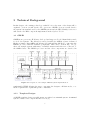
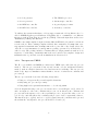
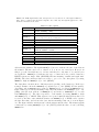
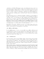
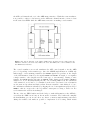
LEON3 processor with the available peripherals. This can be seen in Fig. 3.1 [7],
where an example system with many of available masters and slaves are connected to
the AMBA buses. The LEON3 processor and the other components are described in
Figure 3.1: Depiction of an example LEON3 system implementation.
synthesizable VHDL allowing the user to customize the designs to fill their needs, or to
fit the requirements of platform-specific constraints.
3.1.1
Template Designs
A GRLIB template design generally starts out with a bare minimal system. A minimal
system consists of the components listed below [8].
5
• A clock generator
• The LEON3 processor
• A reset generator
• An interrupt controller
• An AHB bus controller
• A general purpose timer
• An APB bus controller
• A memory controller
To validate the system in hardware, a debug support unit and a debug link needs to be
added. GRLIB supplies several different debug links, able to communicate over different
interfaces such as Joint Test Access Group (JTAG), Universal Asynchronous Receiver
Transmitter (UART), and Ethernet.
GRLIB comes with template designs for many different FPGA development boards from
several vendors. These existing templates include three main files: leon3mp.vhd, config.vhd and testbench.vhd. leon3mp.vhd is the top module of the design, where the
other IP-cores are instantiated. config.vhd is a package generated by an included tool
called xconfig. The package includes constants that set design parameters such as clock
frequency or addressing. testbench.vhd is the test bench for the template design and
instantiates the top module, as well as simulation models if needed.
3.1.2
Two-process VHDL
The IP cores available in GRLIB are written in a VHDL style called the two-process
method. The two-process method has several benefits over the traditional dataflow
method, such as a higher abstraction level and increased readability. The two-process
method also improves simulation times thanks to its use of variables in combinatorial
processes [9].
The two-process method uses the following design rules:
• Using record types in all port and signal declarations.
• Only using two processes per entity.
• Using high-level sequential statements to code the algorithm.
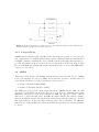
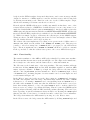
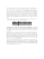
A block diagram showing a two-process circuit can be seen in Figure 3.2 [9], where D
and r are input records to the combinatorial process. rin is driven by the combinatorial
process, and is the input record to the sequential process. r is given the value of rin on
a clock edge, and this allows the combinatorial process to have a sequential behavior.
The functions Q = fq (D,r) and rin = fr (D,r) symbolizes the combinatorial logic and
shows that the only inputs to the process should be D and r [9].
6
Figure 3.2: Block diagram of a generic two-process circuit showing how the combinatorial
and the synchronous process are interconnected.
3.1.3
Plug and Play
GRLIB includes plug and play capability in the way that it is possible to detect the system configuration of a running system using software. This information is implemented
as VHDL constants containing the device identifier, memory mapping and interrupt vector. The information is then accessible as a read-only memory in the bus arbiter. Each
IP-core in GRLIB has a unique ID, and the information can be read by any AHB master
connected to the bus [7].
3.2 AMBA
This section will describe the AMBA system interfaces used in this report. AMBA
is an open standard developed by ARM, and is intended for microcontroller and SoC
development. In this project the following two buses are used:
• Advanced Peripheral Bus (AHB).
• Advanced eXtensible Interface (AXI).
The AHB bus is used as the main system bus in the GRLIB system, while the AXI
bus is used by the HPS system in the Cyclone V SoC. The two standards have many
similarities, but there are some major differences. AHB can only read or write, whereas
AXI can do both at the same time. In AHB, the master handles the address counting,
whereas in AXI the master only supplies the start address and the burst type. A third
important difference is that they have different interconnect structures. In AHB the
system uses a central multiplexer, whereas in AXI, the system uses a crossbar structure
[6, 10, 11].
7
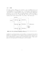
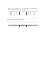
3.2.1
AHB
The high-performance AHB bus is the foundation of the the GRLIB system as can
be seen in Figure 3.1 [7]. AHB supports up to 15 masters and 15 slaves and uses a
central multiplexer to direct the transfers to the correct destination. The multiplexer is
controlled by a decoder which handles the transfer queue and designates which master
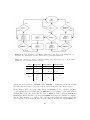
should have access to the bus. The block diagram in Figure 3.3 shows an example of
how the master selection can be configured like. The decoder also decodes the address
currently on the bus and enables the slave corresponding to that address space.
Figure 3.3: Block diagram showing how the AHB decoder selects which master should
have access to the bus by using the HMASTER[3:0] signal [6].
An illustration of the master interface is shown in Figure 3.4; the slave interface is shown
in Figure 3.5. The signals shown in the figures are described in Table 3.1. Please note
that the figures and table do not cover all the signals included in the AHB, but only
those used in this thesis. An AHB transfer between a master and slave consists of three
phases: the bus request phase, the address phase, and the data phase.
8
Figure 3.4: AHB master interface with the different input and output signals shown [6].
Figure 3.5: AHB slave interface with the different input and output signals shown [6].
In the bus request phase, the master that wishes to initiate a transfer begins with the
HBUSREQx signal set high. If the master requires a locked access, the HLOCKx signal is also
set to high. A locked access means that the bus will not be granted to another master
until the HLOCKx signal is set low. When both the HGRANTx signal and the HREADY signal
are high, the bus is granted by the arbiter and the master can start the address phase.
In the address phase the master puts the address on HADDR[31:0] and sets the control
signals. The HWRITE signal is set low if it is a read operation and high if it is a write.
The master sets HTRANS[1:0] to ”10” (NONSEQ), which indicates that this is the first
9
Table 3.1: AHB signal names and description sorted by direction of the signal. Master to
slave, slave to master and arbitration signals. Note that only the signals applicable to this
thesis are included in the table.
HADDR[31:0]
HTRANS[1:0]
HWRITE
HSIZE[2:0]
HBURST[2:0]
HWDATA[31:0]
HRDATA[31:0]
HRESP[1:0]
HREADY
HBUSREQx
HLOCKx
HGRANTx
HSELx
Master to slave signals
Address bus.
Indicates type of current transfers. Can be IDLE,
BUSY, NONSEQ or SEQ.
Indicates if transfer is read or write.
Size of each burst in the transfer. Available options
are: 1, 2, 4, 8, 16, 32, 64 or 128 bytes.
Indicates the burst type used in the transfer.
Write data bus.
Slave to master signals
Read data bus.
Slave response signal. Can be OKAY,
ERROR, RETRY or SPLIT.
Indicates if the slave is ready and/or a transfer is successful.
Arbitration signals
Master bus request signal.
Master locked transfer request signal.
Indicates that the master is granted the bus.
Slave select signal.
address in the transfer. The signal HSIZE[2:0] is set to indicate the size of the data in
the transfer. The size can be set to either 1, 2, 4, 8, 16, 32, 64 or 128 bytes. However, in
this project the bus width is set to 32 bits, and therefore only sizes of 1, 2 and 4 bytes
are applicable. HBURST[2:0] indicates the type of burst used; the possible burst in a
LEON3 system are single ”000” (SINGLE) and incrementing of unknown length ”001”
(INCR). The slave indicates that it is ready to proceed to the data phase by setting
HREADY to high and HRESP[1:0] to ”00” (OKAY).
The data phase can start in two different ways depending on the burst type. If the type
is single transfer, then the HTRANS[1:0] signal is set to ”00” (IDLE) and the master,
depending on how HWRITE was set, writes to HWDATA[31:0] or reads from HRDATA[31:0].
If the burst type is an incrementing burst, then the master sets HTRANS[1:0] to ”11”
(SEQ), puts the next address on HADDR[31:0] and writes to HWDATA[31:0] or reads
from HRDATA[31:0]. The slave responds to each transfer by setting HREADY to high
and HRESP[1:0] to OKAY. This sequence is repeated until the final address has been
received by the slave, after which the master sets HTRANS[1:0] to IDLE, reads or writes
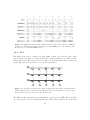
the last data value, and releases the bus. An incrementing burst can be seen in Figure
3.6. The figure includes wait states in both the master and the slave. The master signals
a wait state by setting HTRANS[1:0] to ”01” (BUSY), while the slave does it by holding
HREADY low.
10
Figure 3.6: AHB incrementing burst transfer with wait states as shown in the AMBA 2
specification. The master signals a wait state by setting HTRANS[1:0] to ”01” (BUSY), while
the slave does it by holding HREADY low [6].
3.2.2
AXI
The AXI bus is a more complex bus than AHB, focused on low latency [10]. This
goal is achieved by using a crossbar architecture as shown in Figure 3.7. The crossbar
architecture trades silicon area for a lower latency, as several masters can access the bus
at the same time as long as they do not use the same slaves.
M
M
M
S
S
S
S
S
Figure 3.7: Crossbar bus architecture. Each crossing has a switch that determines which
master (M) has access to which slave (S). This allows several bus masters to use the bus at
the same time as long as they do not use the same slave.
The AXI bus also implements several channels compared to the AHB which only has
one. In total there are five AXI channels: the write address channel, the write data
11
channel, the write response channel, the read address channel, and the read response
channel. A transfer on the AXI bus is divided into three different phases; an address
phase, a data phase and a response phase. However, compared to the AHB bus, the
AXI bus can be in more than one phase at the time as different transfers are performed
across different channels. This means that while a master is writing data on the write
data channel, it can start a new transfer on one of the address channels.
An illustration of the AXI slave interface can be seen in Figure 3.8, showing how it is
divided into different channels. The channels and signals of the AXI slave interface are
described in Table 3.2. Please note that the tables do not cover all the signals included
in the AXI protocol, but only those used in this project.
Figure 3.8: Block diagram of an AXI slave interface, showing the five channels and the
corresponding signals [12].
12
Table 3.2: AXI signals and descriptions for each channel. Note that only the signals
applicable to this project are included in the table.
ARID[n:0]
ARADDR[31:0]
ARLEN[3:0]
ARSIZE[2:0]
ARBURST[1:0]
ARVALID
ARREADY
RID[n:0]
RDATA[31:0]
RRESP[1:0]
RLAST
RVALID
RREADY
AWID[n:0]
AWADDR[31:0]
AWLEN[3:0]
AWSIZE[2:0]
AWBURST[1:0]
AWVALID
AWREADY
WID[n:0]
WDATA[31:0]
WSTRB[3:0]
WLAST
WVALID
WREADY
BREADY
BID[n:0]
BRESP[1:0]
BVALID
Read address channel signals
Read address ID.
Read address bus.
Indicates the number of beats in a burst (1-16).
Size of each burst in the transfer. Available options
are: 1, 2, 4, 8, 16, 32, 64 or 128 bytes.
Indicates the burst type used in the transfer.
Indicates that the address on ARADDR is valid.
Indicates that the slave is ready to receive, or has received
a valid address.
Read response channel signals
Read data ID, needs to be same as ARID.
Write data bus.
Slave response signal. Can be OKAY, EXOKAY, SLVERR
or DECERR.
Indicates the last transfer in a burst.
Indicates that the data on RDATA is valid.
Indicates that the master has received valid data or response.
Write address channel signals
Write address ID.
Write address bus.
Indicates the number of beats in a burst (1-16).
Size of each burst in the transfer. Available options
are: 1, 2, 4, 8, 16, 32, 64 or 128 bytes.
Indicates the burst type used in the transfer.
Indicates that the address on AWADDR is valid.
Indicates that the slave is ready to receive, or has received
a valid address.
Write data channel signals
Write data ID, needs to be same as AWID.
Write data bus.
Indicates the byte lanes with valid data.
Indicates the last transfer in a burst.
Indicates that the data on WDATA is valid.
Indicates that the slave has received valid data.
Write response channel signals
Indicates that the master has received a valid write response.
Write response ID from slave, needs to be same as AWID.
Slave response signal. Can be OKAY, EXOKAY, SLVERR
or DECERR.
Indicates that the write response from the slave is valid
13
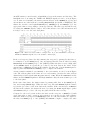
An AXI transfer focuses heavily on handshakes between the master and the slave. The
handshakes are done using the VALID and READY signals as can be seen in Figure
3.9. To start a read transfer, the master puts an address on the ARADDR[31:0] bus, and
asserts that it is a valid address by setting ARVALID high and an ID on ARID[n:0]. The
master also sets the control signals ARSIZE[3:0], ARBURST[1:0] and ARLEN[3:0] to the
appropriate values corresponding to burst type and size. The slave responds when ready
by setting the ARREADY signal to high to show that it has received the information and
is ready to move on to the read data phase.
Figure 3.9: AXI read burst transfer of length four. Note the handshakes between the
VALID and READY signals before the transfer continues [10].
In the read response phase, the slave initiates the response by putting the first data to
be transferred on the RDATA[31:0] bus, and asserts that the data is valid by setting
RVALID high and the RRESP[1:0] to ”00” (OKAY). When the slave receives a high value
on the RREADY signal, it repeats the procedure for the next data in the burst. If the
current data on RDATA is the last in the transfer, the slave also sets the RLAST signal to
high together with RVALID and RRESP[1:0] to complete the transfer.
A write transfer is initiated very similarly to the read transfer, as can be seen in Figure
3.10. The address phase is the same as for a read transfer, but uses the write address
channel instead (the signals with AW-prefix instead of AR). When the AWVALID from the
master and the AWREADY signals are held high simultaneously, the write transfer proceeds
to the data phase.
In the write data phase, the master starts by putting valid data on the WDATA[31:0]
bus, and setting WVALID high. When the slave responds with WREADY high the master
repeats the procedure for the next data in the transfer. If the current data on WDATA is
the last in the transfer, the master shows it by setting the WLAST signal high together
with WVALID, and proceeds to the response phase when the slave is ready.
Compared to the read operation where the slave sends a response on RRESP[1:0] with
every data value, a write operation only generates one response for the entire transfer.
When the master is ready it sets BREADY high, and once the data transfer is completed,
the slave sets BRESP[1:0] to ”00” (OKAY) and BVALID to high to complete the write
14
Figure 3.10: AXI write burst transfer. Note the handshakes between the VALID and
READY signals before the transfer continues [10].
transfer.
As can be seen in Table 3.2, the response signals can return other values than OKAY.
If the access made is exclusive, then the slave should return ”01” (EXOKAY) instead,
otherwise the master will interpret it as an error. The response ”10” (SLVERR) is used
when the slave has encountered an error, and finally the response ”11” (DECERR) is
used when the master tries to access an address where there is no slave.
3.3 Altera Hard Processor System
The Altera Hard Processor System implemented in the Cyclone V SoC FPGA contains
a dual ARM Cortex A9 MPcore processor as well as on-chip memories, flash memory
controllers, an SDRAM controller subsystem and support peripherals. Most important
for this project however, is the interconnect to the FPGA fabric. The HPS features three
AXI bridges to connect to the FPGA fabric of the Cyclone V SoC; the HPS-to-FPGA
bridge, the FPGA-to-HPS bridge and finally the Lightweight HPS-to-FPGA bridge.
The HPS-to-FPGA and FPGA-to-HPS bridges are high performance interconnects connected directly to the main Level 3 AXI switch, while the Lightweight bridge has lower
performance and is connected to one of the Level 3 peripheral switches as shown in
Figure 3.11. The two main bridges can be configured to have a data width of 32, 64 or
128 bits, while the Lightweight bridge has a fixed width of 32 bits. The HPS-to-FPGA
bridge has an address space of up to 960 MB, while the Lightweight bridge only has an
address space of 2 MB. A master on the FPGA side using the FPGA-to-HPS bridge has
access to the entire HPS address space.
The HPS is fully functional in itself, but to be able to use it in an FPGA design, it needs
15
Figure 3.11: Block diagram of the bridge that connects the HPS to the FPGA fabric. The
two main bridges, HPS-to-FPGA and FPGA-to-HPS, can be configured to have data widths
of 32, 64 or 128 bits.
to be instantiated as an IP-core with the Altera Quartus II software using a system
generation tool called Qsys. The instantiation enables the different interfaces available
between the HPS and the FPGA, allowing a user to connect an FPGA design to the
processor system.
There are many configuration options available for the HPS component. However, the
configuration selected for the HPS peripheral pins require the processor to run a bootloader in order for them to take effect [3]. This is because the pin-muxing of all HPS
pins is done during the boot phase of the processor. The boot-loader can be generated
by using the output files from the HPS component generation. Depending on what kind
of configuration is needed, it is also possible to configure the HPS component to match
an already existing boot-loader.
16
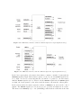
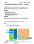
4 Template Design
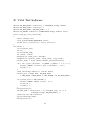
This chapter describes the GRLIB template design for the Altera Cylcone V SoC FPGA
developed in this project. A block diagram of the template design can be seen in Figure
4.1, and implements the following components:
1. Top module: leon3mp.vhd
10. DDR3 controller: ddr3if.vhd
2. AHB-to-AXI bridge: ahb2axi.vhd
11. Debug support unit: dsu3.vhd
3. AHB controller: ahbctrl.vhd
12. General purpose timer: gptimer.vhd
4. JTAG Debug Link: ahbjtag.vhd
13. Interrupt controller: irqmp.vhd
5. AHB Read Only Memory (ROM):
ahbrom.vhd
14. LEON3 processor: leon3s.vhd
6. APB controller: apbctrl.vhd
15. Reset generator: rstgen.vhd
7. APB UART: apbuart.vhd
8. 2 AXI-to-AHB bridges: axi2ahb.vhd
16. Serial Peripheral Interface (SPI) controller: spictrl.vhd
9. 2 Clock generators: clkgen.vhd
17. VGA controller: svgactrl.vhd
Figure 4.1: Block diagram of the Altera Cyclone V SoC template design, showing the
GRLIB cores used as well as the two bridges connecting it to the HPS.
17
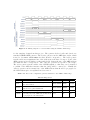
The available resources on the FPGA can be compared to the total resource utilization
of the template design in Table 4.1. The template design operates at a system clock
frequency of 70 MHz and utilizes 27 % of the available logic in the FPGA fabric.
The main logic in Altera FPGAs consists of a building block called Adaptive Logic
Module (ALM). In the Cyclone V each ALM consists of four programmable registers,
two 6-input look-up tables and two full adders [13]. The amount of ALMs needed to
realize a design depends on constraints such as timing. The main embedded Random
Access Memory (RAM) blocks are called M10Ks, and as the name states they can hold
up to 10 Kb of memory each. The M10Ks have customizable port widths and can be
implemented with or without registered outputs [14]. Other resources used are Digital
Signal Processing (DSP) blocks, and Altera Phase Locked Loop (PLL).
Table 4.1: Resource utilization of the entire template design, as well as of its different
sub-modules. ALMs are the main building blocks in Altera FPGAs and stands for Adaptive
Logic Module. The Memory blocks used are Altera M10Ks. Note that these values vary
slightly every time the design is synthesized.
Part Name
ALMs
Memory Blocks
DSP Blocks
PLLs
41910
553
112
15
Total Design
11389.5
100
1
3
leon3mp.vhd
252.9
0
0
0
ahb2axi.vhd
72.9
0
0
0
ahbctrl.vhd
330.3
0
0
0
ahbjtag.vhd
54.2
0
0
0
ahbrom.vhd
6.9
0
0
0
apbctrl.vhd
143
0
0
0
apbuart.vhd
163.9
0
0
0
axi2ahb.vhd (1)
183
4
0
0
axi2ahb.vhd (2)
162.2
4
0
0
clkgen.vhd (1)
0
0
0
1
clkgen.vhd (2)
0
0
0
1
ddr3if.vhd
3322
36
0
1
dsu3.vhd
466.3
8
0
0
gptimer.vhd
147.2
0
0
0
irqmp.vhd
100.3
0
0
0
leon3s.vhd
5224.6
42
1
0
rstgen.vhd
2.8
0
0
0
sld hub (JTAG)
96
0
0
0
spictrl.vhd
236.9
2
0
0
svgactrl.vhd
424.1
4
0
0
Available
18
The following sections will describe several of the components shown in Figure 4.1.
Section 4.1 will go through the decisions concerning the choice of and modifications to
the top module. Section 4.2 explains the implementation of the boot ROM. Section 4.3
will explain the choice of debug link and what impacts it had on the system as a whole.
Section 4.5 explains how the HPS component was instantiated and configured. Section
4.6 describes how the AHB-to-AXI bridge was implemented. Section 4.7 explains the
development of the AXI-to-AHB bridge. Finally, Section 4.8 will explain the APB slaves
implemented.
4.1 Top Module
The top module (leon3mp.vhd) is the wrapper of the entire template design. It contains
all the component instantiations and connects all the peripheral components to their
respective FPGA pins.
To reduce the time it takes to implement a functional template design, the first step was
to see if any of the top modules in already existing template designs could be edited to fit
this project. In the end, the existing template for the Altera Cyclone V E Development
kit was used, as all Cyclone V series FPGAs from Altera use the same technology
mapping. Having the same technology mapping means that template designs utilize the
same versions of hard components such as PLLs and synchronous RAM blocks, which
are used by several IP-cores in GRLIB.
The chosen top module was edited so that all board-specific modules were removed
except for the memory controller wrapper called ddr3if.vhd and the JTAG debug link,
as these were the only peripherals the two boards had in common. The ports and
constraints were also changed to match the Terasic SoCKit board. The old template did
implemented a plain Altera PLL IP-core as a clock generator, which requires the user to
edit the IP-core to change the clock frequency. The Altera PLL was replaced with the
GRLIB clock generator, which also instantiates an Altera PLL, but allows the user to
set the clock frequency through constants in the config.vhd file.
4.2 Boot ROM
To be able to run software on the LEON3 processor, the user needs somewhere to store
the boot loader. Several FPGA development boards have a flash memory and an SD card
socket for storing FPGA bit-files and software images for embedded processors. While
both a flash memory and an SD card socket are available on the SoCKit board, they are
both used by the HPS part of the system and cannot be accessed from the FPGA side,
since the HPS uses them for its booting process. A boot ROM module must therefore
be added to the design so that the LEON3 processor can run software at power-on.
In GRLIB, there is an existing IP for boot ROM called AHB ROM (ahbrom.vhd). Compared to most of the other IP cores, the AHB ROM is unique for each template design.
19
The AHB ROM is generated using software scripts with the boot loader to be stored as
input, and the processor will run the boot loader when the FPGA is programmed with
the bit-file [15].
4.3 Debug Link
To make it possible to validate the system in hardware, a debug link and a debug support
unit have to be included in the template design. There are many available debug links
in GRLIB, however, the options on the SoCKit board are very limited. As the design
should function without the need for any expansion boards, the only possible debug
module is the JTAG link.
The JTAG link introduced a new constraint to the template design, as the system clock
frequency needs to be at least three times as high as the JTAG clock for it to function
[15]. The JTAG clock on the SoCKit board can be set to three different frequencies: 6
MHz, 16 MHz or the default 24 MHz. This means that the system clock frequency needs
to be above 18 MHz, preferably even higher.
4.4 DDR3 Memory Controller
The FPGA side of the Cyclone V SoC has access to an external DDR3 memory of 1
GB. To access the external memory, a memory controller needed to be instantiated and
interfaced to in the template design. An Altera DDR3 memory controller IP-core was
included to interface to the external memory.
The RAM implemented on the SoCKit board consists of two parallel MT41K512M8 low
voltage DDR3 memories from Micron technology Inc [16]. To achieve correct functionality, the memory datasheet was used to determine the different parameters needed to
configure the memory controller.
The memory controller IP uses one of Altera’s own bus protocols, called Avalon, as the
external interface to the rest of the system. However, the memory controller wrapper
ddr3if.vhd from the original template design implements an AHB-to-Avalon bridge.
Therefore, the only major change needed was to replace the old Altera memory controller
instantiation with the new one generated for the SoCKit board.
4.5 HPS component
To be able to interface to the HPS, the HPS component had to be generated. The generation was done by using the Qsys tool included in the Altera Quartus II software. The
HPS component can be configured in many different ways divided into four categories:
FPGA interfaces, peripheral pins, HPS clocks, and SDRAM.
The FPGA interfaces category contains the configuration options for all the available
connections between the HPS and the FPGA fabric. It is in this category that the
20
configuration of the HPS AXI interfaces is done. As explained in Section 3.3, there are
three general purpose bridges; the HPS-to-FPGA bridge, the FPGA-to-HPS bridge, and
the lightweight HPS-to-FPGA bridge. For this project all these bridges were enabled
and set to a width of 32 bits, since they are to be bridged to the AHB bus which is 32
bits wide. It is also possible to enable FPGA-to-HPS interrupts and an AXI interface
connected directly to the HPS memory controller, but those options are not included in
this design.
The peripheral pins category contains the pin-muxing configuration options available in
the HPS. As explained in Section 3.3, the activation of the pin-muxing in the HPS is
dependant on the boot-loader image used. The configuration selected in the peripheral
pins category does therefore not affect the HPS pin-muxing when the FPGA is programmed. Instead, when the HPS component is generated, Qsys will also generate the
files needed to create a boot-loader which performs the pin-muxing. In this project, the
Linux image delivered with the board was used to boot the HPS and a new boot-loader
was therefore not needed. Anyhow, the peripheral pins were still configured according
to the Linux image to avoid any possible errors in the synthesis tool.
In the HPS clocks tab the configuration was left to the default settings, while in the
SDRAM category the HPS memory controller was configured the same way as the Altera
memory controller IP used on the FPGA side of the system.
4.6 AHB-to-AXI Bridge
For the GRLIB system to be able to access the HPS bus, an AHB-to-AXI bridge had
to be implemented. In this case, there was already an existing bridge available in the
GRLIB template design for the Digilent ZYBO board called ahb2axi.vhd. To reduce
development and verification time, it was decided to modify and implement the existing
bridge in the design for the SoCKit board.
4.6.1
Modifications
One issue with the bridge from the ZYBO template design is that it supports single
write and incrementing read bursts, which partially violates the AHB-to-AXI bridge
design guidelines from ARM [17]. The guidelines state that all incrementing bursts of
unknown length should be converted to single transfers, and since GRLIB only supports
single transfers and incrementing bursts of unknown length, all transfers on the AXI side
should be single transfers.
While it is fully possible to implement a bridge that supports all burst lengths, it would
require that the AXI master always makes maximum length bursts, and then the AHB
master that requested the read transfer throws away the remaining data when it is
finished. This method might lead to data being lost if the read transfer targets a memory
address containing for example a First In First Out (FIFO) buffer. The reason why the
21
bridge from the ZYBO template design used this feature, was because it was specifically
designed to interface to a DDR3 memory controller, and there was no risk of losing data
by allowing incrementing reads. This is not the case for the SoCKit template design,
and the incrementing read feature was therefore removed.
Even though the GRLIB address space is fully customizable in hardware, some of the
software libraries related to GRLIB have default addresses for some components, for example the default RAM address begins at 0x40000000 [18]. Another default region is the
AMBA plug and play information which lies at 0xFFFFF000-0xFFFFFFFF, and directly
interferes with the HPS peripheral region which is located at 0xFC000000-0xFFFFFFFF
[3]. While it is simple enough to restructure the address space in the GRLIB system,
adding an offset to the AXI addressing was deemed a better and simpler solution. That
way, the default addresses could be kept as they are.
The address offset was implemented by adding a new generic in the SoCKit version of
ahb2axi.vhd, which sets the widths of the AWADDR and ARADDR ports. This way it is
possible to select how many bits of HADDR should be propagated to the AXI address
space. The most significant bits of AWADDR and ARADDR can then be added as constants
in the top module, so that the address buses point to the correct AXI address region.
4.6.2
Functionality
The transfer translation of the AHB-to-AXI bridge is handled by a finite state machine.
The state machine has six states as shown in Figure 4.2. The ellipse is the initial state,
the rectangles are other states, and the diamonds are conditional transitions.
The Idle state is the default state of the state machine. The state machine will wait
in this state holding HREADY high and the AXI handshake signals low, until an AHB
master requests a transfer. If HSELx goes high, the bridge will store the first address
and the control signal HSIZE, and then transition to Write 1 if HWRITE is high, or Read
1 if HWRITE is low. A timing diagram of a write transfer can be seen in Figure 4.3 and
a read transfer in Figure 4.4.
In the Write 1 state, the bridge stores the data coming in on HWDATA and determines
the AXI control signals. Since the bridge only makes single transfers, the value of AWLEN
is always set to one transfer. AWBURST is set to incrementing burst and AWSIZE is set to
the same value as HSIZE. To make sure that the AXI slave reads from the correct byte
lanes when writing halfword or byte, the signal WSTRB is used to indicate which byte
lanes are active according to big-endian addressing. This is because the GRLIB system
uses big-endian addressing, while the HPS uses little-endian addressing. The active byte
lanes depending on system endianness is shown in Table 4.2. By using the WSTRB signal
this way, the data does not have to be switched around to achieve the correct endianness.
The bridge then initiates the AXI transfer by moving on to the Write 2 state.
In the Write 2 state, the bridge starts the AXI transfer by holding AWVALID high, and
22
Figure 4.2: State diagram for the AHB-to-AXI bridge. The ellipse is the initial state, the
rectangles are other states, and the diamonds are conditional transitions.
Table 4.2: Active byte lanes for different transfer sizes when using big- or little-endian
addressing on a bus with a width of 32 bits.
Size
Addr[1:0]
Word
”00”
3
3
3
3
3
3
3
3
”00”
3
3
-
-
-
-
3
3
”10”
-
-
3
3
3
3
-
-
”00”
3
-
-
-
-
-
-
3
”01”
-
3
-
-
-
-
3
-
”10”
-
-
3
-
-
3
-
-
”11”
-
-
-
3
3
-
-
-
Halfword
Byte
Big-endian
Little-endian
putting the stored address on AWADDR. When AWREADY goes high, the bridge knows that
the addressed slave has received the address, and transitions to the Write 3 state.
In the Write 3 state, the bridge immediately sets AWVALID to low; otherwise the slave
accessed might interpret a high value on AWVALID as a new transfer on the write address
channel. The bridge also shows that the data on WDATA, is valid by holding WVALID and
WLAST high. When the slave responds with WREADY held high, the transfer is complete,
and the state machine goes back to Idle. Worth noting is that the bridge ignores the
write response but prevents the slave from freezing by holding the signal BREADY at a
23
constant high. The reason for ignoring the response is that the ”OKAY” response is
the only possible answer. The ”EXOKAY” response is only used for exclusive accesses,
which the bridge does not make. The ”SLVERR” response is only used together with
error control coding, which is not used. Finally the the ”DECERR” response is used
when a master tries to access an address that does not exist, which cannot happen in
this implementation, and can not be propagated to the AHB side.
Figure 4.3: Timing diagram of a write transfer using the AHB-to-AXI bridge.
In the Read 1 state, the bridge holds HREADY low while making the AXI transfer. The
bridge puts the stored address on ARADDR and holds ARVALID high to indicate that the
address is valid. The ARSIZE signal is always set to indicate a word-size transfer, no
matter what HSIZE is set to. This way the issue with different endianness can be ignored.
ARBURST is set to incrementing burst, and ARLEN is set to indicate that it is a single
transfer. When the target slave responds with ARREADY held high, the bridge moves on
to the Read 2 state.
In the Read 2 state, the bridge immediately sets ARVALID to low; otherwise the slave
accessed might interpret a high value on ARVALID as a new transfer on the read address
channel. It also holds RREADY high to indicate that it is ready to receive the data response
from the slave. When the slave responds with valid data (RVALID and RLAST held high,
the transfer is complete and it returns to the Idle state.
4.6.3
Instantiation
The bridge instantiation can be configured in several different ways according to the
generics described in Table 4.3, where the right-most values in the table are the one used
24
Figure 4.4: Timing diagram of a read transfer using the AHB-to-AXI bridge.
for the template designed in this project. The generics hindex, haddr and hmask are
standard GRLIB AHB generics. The hindex generic sets the AHB slave index, which
is used to determine which HSELx the slave should correspond to. The haddr generic
sets the twelve most significant bits of the address area the slave belongs to. Last of the
AHB generics is hmask which, together with haddr, defines the size of the AHB address
area that the slave corresponds to. The other two generics are specific to the bridge.
The idsize generic sets the width of the AXI ID signals, so that they can be matched
to widths of the AXI slave interface that the bridge will be connected to. Finally the
addrsize generic sets how many bits of the AHB address that should be propagated to
the AXI address space as explained in Section 4.6.1.
Table 4.3: List of the configurable generics available for the AHB-to-AXI bridge.
Name
hindex
haddr
hmask
idsize
addrsize
ahb2axi.vhd generics
Description
AHB slave index.
AHB address, sets the 12 most significant
bits of the address.
AHB address mask, sets the size of the
address area together with haddr.
Width of the AXI ID signals.
Width of the AXI address buses. Determines
how many bits of the AHB address that shoud
be propagated to the AXI domain.
25
Range
0-15
Default
0
Used
3
0x000-0xFFF
0x000
0xCF0
0x000-0xFFF
0xFFF
0xFF0
1-32
8
8
1-32
32
28
Since the HPS peripheral region is located at 0xFC000000, but the AHB bridge address
is set to 0xCF000000, addrsize was set to 28. An offset was added in the top module
by setting the four most significant bits to 0xF, so that the AXI addresses start at
0xFF000000. The reason not having the AXI addresses start at 0xFC000000 is that
the first addresses in the peripheral region belong to the HPS debug access port and
the lightweight HPS-to-FPGA bridge, and it was deemed unnecessary to include those
peripherals.
The input and output ports of the bridge consists of a clock and a reset as well as all
the AHB slave interface signals and AXI master interface signals as shown in Section
3.2.2. The AHB interface signals are connected to the AHB bus and the AXI signals are
connected to the AXI slave interface on the HPS component.
4.7 AXI-to-AHB Bridge
For the HPS system to access the GRLIB address space, an AXI-to-AHB bridge had to be
implemented. This bridge had to be designed from scratch since no freely available usable
IP-core was found. This Section describes the requirements, choices and functionality of
the developed bridge.
4.7.1
Design Requirements
To make sure that the bridge works as intended, several requirements had to be fulfilled:
• The bridge must have a functional AXI slave interface able to communicate with
the AXI master interface in the hard subsystem. To reduce latency, it should also
be able to accept write and read requests at the same time.
• The bridge must have a functional AHB master interface able to communicate
with the rest of the GRLIB system. The AHB master interface needs to be able
to request the bus, and to handle address counting during burst transfers.
• The bridge needs to handle burst transfers of up to 16 transfers, since it is the
maximum burst length AXI can handle.
• The bridge should handle transfer sizes of word, halfword and byte.
• The bridge needs to translate the transfer endianness.
4.7.2
Design Choices and Functionality
A block diagram of the resulting AXI-to-AHB bridge can be seen in Figure 4.5. The
bridge consists of five parts; the AXI slave interface, the write data FIFO, the read data
FIFO, the control translator, and the AHB master interface. The functionality of the
bridge is handled by three finite state machines: one for the AXI write channels, one for
26
the AXI read channels and one for the AHB master interface. With three state machines,
it is possible to achieve a low latency, as the AXI write channel interface can store data
in the write data FIFO while the AHB master interface is making a read transfer.
Figure 4.5: Block diagram of the AXI-to-AHB bridge showing the five main parts; the
AXI slave interface, the write data FIFO, the read data FIFO, the control translator and
the AHB master interface.
The control translator stores and translates the AXI control signals to fit the AHB
protocol depending on the transfer type. Since the GRLIB implementation of AHB only
makes single or incrementing transfers, the HBURST signal is dependent on the length
of the AXI transfers defined by the signals AWLEN and ARLEN. A length of one signifies
a single transfer; other lengths sets the burst type to incrementing. During a write
transfer, the HSIZE signal is the same as AWSIZE, while during a read transfer, HSIZE is
always set to word. By always having the size of word during AHB reads, the endianness
of the transfer does not have to be translated as the active byte lanes for word transfers
are the same in big-endian and little-endian. In write transfers of size halfword or byte,
the endianness translation is handled by flipping the two least significant address bits of
HADDR so that it corresponds to the big-endian counterpart according to Table 4.2. For
word transfers the address is unchanged.
The use of the two FIFO buffers enable the bridge to make full transfers on the AXI side,
even when the AHB bus is busy at the moment of transfer. The buffers also simplify
the handshaking process in case there are slaves or masters implementing wait states
during the transfer, and makes it possible to implement clock crossing, which means
27
that the two bus interfaces can run on different clock frequencies. In this bridge, the
clock crossing is limited to the case where the AXI clock runs at a higher frequency.
The values written to the write FIFO depend on the WSTRB signal. When the transfer size
is byte, the byte in the active byte lane is written to all byte lanes in the write FIFO. The
same procedure is used for for halfword as can be seen in Table 4.4. For word transfers
the data is unchanged. The reason for not just mirroring the data for byte and halfword
transfers is that the AXI transfers are not address aligned, but transfer order aligned.
This means that when making a transfer smaller than word, the first data will always
be aligned to the least significant part of the data bus, and not according to the address
[10].
Table 4.4: An example of how the byte ordering for write transfers is handled in the write
FIFO depending on the value of the WSTRB and AWSIZE signals.
AWSIZE
BYTE
HALFWORD
WORD
WSTRB
”0001”
”0011”
”1111”
WDATA[31:0]
0x12
0x1234
0x12345678
WFIFO[31:0]
0x12121212
0x12341234
0x12345678
The FIFO buffers are implemented using the GRLIB Syncram 2P IP-core [15]. The
Syncram 2P IP-core uses the technology mapping of the template design to instantiate
the two-port block RAM available in the targeted FPGA. Implementing the buffers this
way greatly reduces the area usage, since dedicated memory resources are used instead
of logic slices.
The AXI interface state machines are independent of each other, while the AHB state
machine depends on control signals from either of the two AXI state machines. Those
signals, called inter-state control signals, can be seen in Table 4.5. The AHB_W_EN,
AHB_W_ACK and AHB_W_DONE are used between the AXI write and the AHB master state
machine, while the AHB_R_EN and AHB_R_DONE are used by the AXI read and the AHB
master state machine. The FIFO data pointer signals are used to count the data going
in and out of the corresponding FIFO buffer.
A flow chart for the AXI state machines can be seen in figure 4.6. The flow chart to the
left in the figure is for the AXI write states, while the one to the right is for the AXI
read states. The flow chart for the AHB state machine can be seen in Figure 4.7. The
ellipses are the default states, the rectangles are the other states, and the diamonds are
conditional transitions. Sections 4.7.2.1, 4.7.2.2 and 4.7.2.3 will explain the AXI-to-AHB
bridge state machines in more detail.
28
Table 4.5: Table showing the control signals used between the AXI and AHB state machines, as well as the FIFO buffers.
Inter-state control signals
4.7.2.1
AHB W EN
Write enable. Initiates AHB write transfer.
AHB W ACK
Write acknowledge. AHB write transfer is started.
AHB W DONE
Write transfer complete. Write data FIFO is empty.
AHB R EN
Read enable. Initiates AHB read transfer.
AHB R DONE
Read transfer complete. Data is available in read FIFO.
WFIFO W PTR
Write FIFO pointer, write address to the write FIFO.
WFIFO R PTR
Write FIFO pointer, read address to the write FIFO.
RFIFO W PTR
Read FIFO pointer, write address to the read FIFO.
RFIFO R PTR
Read FIFO pointer, read address to the read FIFO.
AXI Write States
In the W Start state, the state machine waits for an AXI write request by holding
AWREADY high, indicating that it is ready to receive a valid write address. If AWVALID
goes high, there is a valid address on the AWADDR bus and the state machine transitions
to the W Wait state.
In the W Wait state the state machine stores the address and control signals AWSIZE,
AWLEN, AWBURST and AWID, supplied from the master requesting the transfer. It also sets
AWREADY low to indicate that the address channel is busy. If AHB_W_DONE is high the
state machine transitions to the W Data FIFO state. The AHB_W_DONE signal indicates
that the AHB master is finished with the write FIFO and that the current data in it can
be overwritten.
In the W Data FIFO state, the state machine stores valid data in the write FIFO buffer.
If the WVALID signal is high, the state machine sets WREADY high and stores the data
from WDATA in the write FIFO at the position indicated by WFIFO_W_PTR. If WVALID is
accompanied by WLAST held high, the transfer is finished and it transitions into the W
AHB state. If WLAST is low, it indicates that there is more data coming, and the state
machine repeats the W Data FIFO state with WFIFO_W_PTR incremented by one.
In the W AHB state, the state machine holds AHB_W_EN high to indicate to the AHB
state machine that the write FIFO contains valid data, and that it should request the
bus for a write transfer. If AHB_W_ACK goes high, it indicates that the AHB master is
requesting the bus for a write transfer, and the state machine transitions into the W
Done state.
In the W Done state, the state machine sets AHB_W_EN low and sends the write response
to the master which requested the transfer. The response is made by holding BVALID
high, while putting the ”OKAY” response on BRESP, and the transfer ID stored during
29
Figure 4.6: State diagrams for the AXI-to-AHB bridge AXI slave interface showing the
write states to the left, and read states to the right. The ellipse is the initial state, the
rectangles are other states, and the diamonds are conditional transitions.
the W Wait state on BID. When the master indicates that it has received the response
by holding the BREADY signal high, the transfer is complete and the state machine goes
back to the Start state.
4.7.2.2
AXI Read States
In the R Start state, the state machine waits for an AXI read request by holding ARREADY
high, indicating that it is ready to receive a valid read address. If ARVALID goes high,
there is a valid address on the ARADDR bus and the state machine transitions to the R
Wait state.
In the R Wait state, the state machine tells the AHB master to request the bus for
a read transfer by holding AHB_R_EN high. It stores the address on ARADDR and the
control signals ARSIZE, ARLEN, ARBURST and ARID, supplied from the master requesting
the transfer. It also sets ARREADY low to indicate that the address channel is busy. When
the AHB_R_DONE goes high, the AHB master has finished the read transfer and the state
30
Figure 4.7: Flow chart for the AXI-to-AHB bridge AHB master interface state machine.
The ellipse is the initial state, the rectangles are other states, and the diamonds are conditional transitions.
machine then transitions to the R Data FIFO state.
In the R DATA FIFO state, the state machine reads the data from the read FIFO and
puts it on the RDATA bus. It also signals that the data is valid by holding RVALID high,
RRESP set to ”OKAY”, and RID to the same value as the ARID value stored in the R Wait
state. If RFIFO_R_PTR is equal to the stored value of ARLEN, the state machine sets RLAST
high and transitions to the R Start state. If RFIFO_R_PTR not equal to ARLEN, the state
machine repeats the R Data FIFO state with RFIFO_R_PTR incremented by one.
4.7.2.3
AHB Master States
In the Idle state, the AHB master awaits orders from any of the two AXI state machines.
While idle, it holds HTRANS set to ”IDLE”, holds AHB_W_DONE high and AHB_R_DONE low.
If AHB_W_EN goes high or AHB_R_EN it transitions to the Bus Request state. If both go
high at the same time, write operation has the highest priority.
In the Bus Request state, the AHB master requests the bus by setting HBUSREQx high.
It also translates and stores the control signals from the stored by the AXI interface. If
it is a write operation, HWRITE is set high, otherwise low. If HGRANTx and HREADY goes
high, the AHB master transitions to the Address Phase state.
31
In the Address Phase state, the AHB master puts the first address on the HADDR bus
and sets HTRANS to ”NONSEQ”. The master uses the burst length to calculate the final
address of the transfer. If the current address is equal to the final address it transitions
to the Last Data state, otherwise it transitions to the Data Phase state.
In the Data Phase state, the AHB master increments the address depending on the size
of the transfer, and sets HTRANS to ”SEQ”. If it is a write transfer, the data from the
write FIFO is put on HWDATA, else if it is a read transfer, the data on HRDATA is stored in
the read FIFO. If the current address is equal to the final address, it transitions to the
Last Data state, otherwise the Data Phase state is repeated.
In the Last Data state, the AHB master sets HTRANS to ”IDLE” and HBUSREQx to low. If
it is a write transfer, the last data from the write FIFO is put on HWDATA and the master
transitions to the Idle state. If it is a read transfer, the last data on HRDATA is stored in
the read FIFO and the master transitions to the Read Done state.
In the Read Done state, the AHB master indicates that the read transfer is done to the
AXI read state machine by setting AHB_R_DONE high. When the AXI read state machine
responds by setting AHB_R_EN low, the master transitions to the Idle state.
4.7.3
Performance
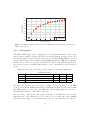
The theoretical performance of the AXI-to-AHB bridge can be described by the following
equation:
L
Rb = fclk · Nb ·
(k + 2L)
Here Rb is the transfer rate in bits per second, fclk is the system clock frequency, Nb is
the width of the data bus in bits, L is the burst length of the transfer, and k is the clock
cycle overhead introduced by the bridge.
The k-value depends on several different factors, such as the number of wait-states
required by an accessed slave, or the number of clock cycles before the AHB master
interface is granted the bus. The minimum k-value can be derived from the state machines and verified in simulations. For write transfers kW,min = 7, while for read transfers
kR,min = 6. Using the minimum values of k, the transfer efficiency of a 32 bits wide
bridge can be said to be between 3.6 and 13.5 data bits per clock cycle.
Figure 4.8 shows transfer rates for write and read transfers with fclk = 70 MHz, different
values of L, and using the minimum k-value. As can be seen, the transfer rate of the
bridge increases with the burst length, since a higher burst length makes the bridge
overhead less significant.
32
1000
900
Bit Rate (Mb/s)
800
700
600
500
400
300
Write Transfer
Read Transfer
200
0
2
4
6
8
10
12
14
16
Burst Length (L)
Figure 4.8: Transfer rates for write and read transfers with different burst lengths at 70
MHz clock frequency.
4.7.4
Instantiation
The AXI-to-AHB bridge can be configured in a few ways when instantiated. The configurable generics available are shown in Table 4.6, and the right-most values are the ones
used in this template design. The generic hindex is a standard GRLIB AHB generic and
sets the master index, and determines which HGRANTx signal the AHB master interface
should react to. The idsize generic determines the width of the AXI ID signals used.
The memtech generic determines which library to use to instantiate dedicated memory
blocks.
Table 4.6: List of the configurable generics available for the AXI-to-AHB bridge.
Name
hindex
idsize
memtech
axi2ahb.vhd generics
Description
AHB master index.
Width of the AXI ID signals.
Technology mapping for the FIFO buffers.
Range
0-15
1-32
0-ntech
Default
0
6
0
Used
2
12
Altera
The input and output ports of the bridge consists of a reset, an AXI clock, an AHB
clock, as well as all the AHB master interface signals and the AXI slave interface signals.
The AHB signals are connected to the AHB bus, and the AXI signals are connected to
the AXI master interface on the HPS component.
Since the bridge only has an address space 960 MB on the HPS side, the two most
significant bits of the addresses need to be hard coded to target the desired GRLIB
address area. For this project, the main bridge was set to target the memory controller,
33
while the lightweight bridge was set to target the APB slaves.
4.8 APB Slaves
This section will explain the choices behind the APB slaves implemented in the template
design. The interrupt controller and the timer are required by default and the reasoning
behind them will therefore not be explained any further.
4.8.1
UART
When running a Linux kernel on the LEON3 processor, or any software that produces
output on a terminal, a UART IP core must be present in the system [8]. The SoCKit
board does not have any UART connection on the FPGA side, but the APB UART can
still receive and send data by running the core in debug mode [15]. When the UART is
in debug mode, it uses a separate pair of FIFO buffers which are accessed by the active
debug link so that the GRMON2 debug tool can be used as a terminal.
4.8.2
SPI Controller
The SPI controller was implemented to allow for software tests targeting a GRLIB
peripheral in the FPGA fabric. The SPI controller is interfaced to a temperature sensor
on the SoCKit board [5].
4.8.3
VGA Controller
The GRLIB VGA controller core was implemented to test the performance of the AXI-toAHB bridge from the HPS side while the AHB bus is under heavy load, and is interfaced
to the VGA DAC on the SoCKit board [5, 15]. The VGA controller implements a frame
buffer in the system memory, which it reads from using an AHB master interface. The
VGA master interface puts a very high load on the AHB bus, since it must read the
entire frame buffer from the memory every time the screen should be refreshed. In this
case a screen resolution of 640 times 480 pixels was used, and with 32 bits per pixel,
gives the frame buffer a size of 1200 kB.
34
5 System Verification and Testing
This chapter describes the verification and validation process of the project. The verification and validation was split into three steps. The first step was the verification
in simulation and test benches which is explained in Section 5.1. The second was the
validation in hardware using the GRMON2 debug tool; this process is explained in Secion 5.2. The third and final step was to run software on the two processor systems and
observe their behavior, which is described in Section 5.3.
5.1 Test Benches
Two test benches have been used in this project. The first test bench was the system
test bench which is included in every GRLIB template design. The second one was a
modified version of the first, used to verify the functionality of the AXI-to-AHB. Both
test benches were run using Mentor Graphics ModelSim 10.0c.
5.1.1
System Test Bench
In GRLIB, there is a separate test bench for every template design. The system test
bench is designed to emulate the prototype board on which the template design should
be implemented [7].
The test bench instantiates the top module of the template design, scans the bus, and
runs a test program. The test program is a boot loader run from the ROM, which
initializes the processor and peripherals such as the memory controller. If a module in
the design does not fit with the AMBA standard, or if any of the peripherals cannot be
initialized, then the simulation fails [7].
5.1.2
AXI-to-AHB Test Bench
To be able to properly simulate the functionality of the AXI-to-AHB bridge, a test bench
was needed. The system test bench was modified to include a dummy AXI master, and
an altered version of the top module (leon3mp.vhd). To simplify the testing, the altered
version of the top module had the HPS component and the DDR3 memory controller
components removed. The bridge’s AXI slave interface was instead connected to the
dummy AXI master and an AHB RAM component was instantiated to replace the
DDR3 memory controller.
In the test bench, the dummy AXI master writes every burst length (1 to 16) of size
word targeting the AHB RAM; then it does the same for sizes halfword and byte. When
35
all the writes have been completed, the AXI master reads back all the values in the same
fashion. The read values are then be compared to the ones written to verify the bridge
functionality. Since the test bench is based on the system test bench, it also prints all
the AHB bus transfers made, and reports illegal transfers, during the run.
5.2 Validation in Hardware
Once the test benches had been passed, the design was synthesized and implemented on
the FPGA, and GRMON2 was used to connect to the system via the JTAG. By using
GRMON2 to issue bus writes and reads, it was possible to test if the system bus was
functional.
The AHB-to-AXI bridge was tested by writing and reading from the HPS UART peripheral, which was connected to a PC. Once the system was tested through GRMON2,
it was tested by successfully loading and booting Linux on the LEON3 processor.
5.3 Software Tests
Various software tests were written and run on the LEON3 and HPS to fully test the
bridges. The endianness translation of the AXI-to-AHB bridge was tested by having
both the HPS and LEON3 access the GRLIB SPI controller to read from the board temperature sensor. If both processors printed the same value, and the value was reasonable,
then the test was assumed to be passed.
A similar test was made for the AHB-to-AXI bridge by drawing an image on the LCD
screen connected to the HPS from both the HPS and LEON3. If the image drawn by
the LEON3 processor appeared correct, the test was passed.
Burst accesses on the AXI-to-AHB bridge were tested by making burst write and read
accesses to the FPGA DDR3 memory from the HPS.
5.3.1
Bridge Performance
The performance of the AXI-to-AHB bridge was tested by measuring the time it took
to read a VGA frame from the HPS memory, and then write it to the DDR3 memory on
the FPGA side. The burst transfers were made using the C library function memcpy(),
and the main code with comments can be seen in Appendix B.
The results of the measurements are shown in Table 5.1. As can be seen, the measured
values are lower than the theoretical ones derived in Section 4.7.3. The reason for the
much lower values can be explained by the fact that the time measured includes several
other operations other than just the transfer across the bridge. For example the processor
has to read from its own memory first, and then the data must pass the L3 interconnect
before even arriving at the bridge.
36
Table 5.1: Transfer measurements done on the AXI-to-AHB bridge when the AHB is free,
and the bridge AHB master is the only active master.
Transfer type
Burst Length
Write
1
Write
2
Read
8
Data Size (bits)
9830400
Time (ms)
Bit Rate (Mb/s)
72.2
136.5
39.1
251.7
26.4
373.0
Another important factor for the bridge performance is whether the AHB bus is free
or busy. Table 5.2 shows the transfer rates for when the bridge AHB master has to
compete for the ownership of the bus against another master. As can be seen the bit
rate is almost half of that when the bus is free.
Table 5.2: Transfer measurements done on the AXI-to-AHB bridge when the AHB is busy,
and the bridge AHB master is competing for ownership of the bus with another master.
Transfer type
Burst Length
Write
2
Read
8
Data Size (bits)
9830400
37
Time (ms)
Bit Rate (Mb/s)
71.5
137.4
46.9
209.6
6 Discussion
A GRLIB template design has been developed for the Cyclone V SoC FPGA implemented on the Terasic SoCKit board running at 70 MHz. It includes several GRLIB
IP-cores, as well as an AHB-to-AXI bridge and a newly developed AXI-to-AHB bridge,
connecting the FPGA fabric to the Altera HPS present on the chip.
The developed AXI-to-AHB bridge has a theoretical average transfer efficiency of between 3.6 and 13.5 bits per clock cycle for 32-bit transfers. The efficiency is dependent
on the transfer burst length where the maximum burst length of 16 is the most efficient.
The efficiency is further reduced if the AHB bus is busy at the time of transfer.
The template design demonstrates how the GRLIB IP-cores can be connected to the
Altera HPS. With this knowledge, GRLIB users can reduce their power consumption
and their board sizes by switching to SoC FPGAs; compared to using the current setup
consisting of separate microprocessor and FPGA chips.
It is important to note that it is not mandatory to include the LEON3 processor in the
design. The LEON3 processor can be deselected during the configuration of the design
if it is not needed. Not including the LEON3 processor reduces the total area usage of
the design by around 45 %.
6.1 Possible Uses
There are several possible uses for the template design and the bridges developed during
this project. The main use for the template design is to demonstrate that the GRLIB
IP-cores such as the SpaceWire controller can be used and interfaced to the Altera HPS.
One major benefit with the GRLIB IP-cores is that they are portable between FPGA
vendors. The portability means that the bridges can be implemented on similar SoC
FPGAs, which implement a hard processor to FPGA AXI interface, such as the Xilinx
Zynq-7000 or the Microsemi SmartFusion2 [19, 20]. No such porting effort has been
made during this project.
The AXI bus uses a lot of area due to its crossbar structure. If area is a limiting factor, it
could be possible to implement an AHB subsystem for non-critical peripherals to reduce
the total area utilization. This AHB subsystem could then be connected to the main
AXI bus using the AXI-to-AHB bridge.
6.2 Further Development
Even though the design is functional, it can still be improved. One change which could
be implemented would be to add control registers to the bridges, which would allow for
38
a soft setting of the address offset. This improvement would allow the target address
space of the bridges to be moved during run-time. Having a movable address space
would allow for one bridge to access the entire GRLIB address space.
A useful component, which could be added to the design would be a mailbox component.
A mailbox is a similar to a bridge in the way that it consists of two buffers, but instead
of being a slave-to-master interface, it is slave-to-slave. The mailbox works by having
two memories, where the write interface is connected to one bus, while the read interface
is connected to the other as can be seen in Figure 6.1. When one of the processors wants
to send data to the other one, it writes to the mailbox. When write is complete, the
mailbox can trigger an interrupt, or set a flag to signal the receiver that there is data
available for processing.
Figure 6.1: Block diagram of a mailbox component, a bridge with two slave interfaces.
6.3 Time Plan
The project was executed with few deviations from the original time plan, which can be
seen Figure A.1 in Appendix A. The most notable deviation is the fact that the AXIto-AHB bridge was not a part of the original plan, but added later during the project.
This change was made due to the fact that AHB-to-AXI bridge took far less time to
implement than planned, and that a bridge from the HPS to the GRLIB system was
a logical addition to the template design. Another deviation was that the UART and
Ethernet peripherals had defined time slots separate from the bridge itself. The reason
for them being separate was because the time plan was made before the HPS-to-FPGA
interconnect was studied in detail.
39
7 Conclusion
During the course of this project, a working GRLIB template design has been developed
for the Cyclone V SoC FPGA implemented on the Terasic SoCKit board. The template
design implements the LEON3 processor core, several peripheral IP-cores from GRLIB,
an AHB-to-AXI bridge, and a newly developed AXI-to-AHB bridge.
The template design operates at a system clock frequency of 70 MHz and uses about
27 % of the logic resources available in the FPGA fabric. The design was verified in
simulation using the GRLIB system test bench, and validated in hardware using the
GRMON2 debug tool, and custom made software.
The AXI-to-AHB and the AHB-to-AXI bridges are connected to the Altera HPS included
in the SoC FPGA using the available AXI interfaces. The bridges allows the HPS to
access the GRLIB template design AMBA bus, and the GRLIB system to access the
Altera HPS peripherals.
The AHB-to-AXI bridge is a low performance bridge which only accepts single transactions, while the AXI-to-AHB bridge can accept bursts of up to 16 transfers. The
AXI-to-AHB bridge implemented in the template design is a buffering bridge with a
theoretical transfer rate of up to 13.5 bits per clock cycle. The bridges have been developed with portability in mind so that they can be used to interface to similar hard
subsystems from other FPGA vendors, such as the Xilinx Zynq-7000 SoC.
40
Bibliography
[1] GRLIB Product Brief. Cobham Gaisler AB. Accessed: 2015-01-29. [Online].
Available: http://www.gaisler.com/doc/Leon3%20Grlib%20folder.pdf
[2] IGLOO2 Product Information Brochure. Microsemi. Accessed: 2015-05-07. [Online].
Available:
http://www.microsemi.com/document-portal/doc download/132013igloo2-product-information-brochure
[3] Cyclone V Hard Processor System Technical Reference Manual. Altera. Accessed:
2015-01-19. [Online]. Available: http://www.altera.com/literature/hb/cyclonev/cv 5v4.pdf
[4] Zynq-7000 Overview. Xilinx. Accessed:
2015-05-07. [Online]. Available:
http://www.xilinx.com/support/documentation/data sheets/ds190-Zynq7000-Overview.pdf
[5] SoCKit User Manual. Terasic. Accessed:
2015-01-19. [Online]. Available:
http://www.terasic.com.tw/cgi-bin/page/archive download.pl?Language=
English&No=816&FID=a9e8cb474881606fa975d2420a309fb6
[6] AMBA Specification Rev. 2.0. ARM. Accessed: 2015-03-09. [Online]. Available:
http://www-micro.deis.unibo.it/˜magagni/amba99.pdf
[7] GRLIB IP Library User’s Manual. Cobham Gaisler. Accessed: 2015-02-23. [Online].
Available: http://www.gaisler.com/products/grlib/grlib.pdf
[8] LEON/GRLIB Configuration and Development Guide. Cobham Gaisler AB.
Accessed: 2015-03-24. [Online]. Available: http://www.gaisler.com/products/
grlib/guide.pdf
[9] Fault-tolerant Microprocessors for Space Applications. Cobham Gaisler. Accessed:
2015-03-20. [Online]. Available: http://www.gaisler.com/doc/vhdl2proc.pdf
[10] AMBA AXI Protocol. ARM. Accessed: 2015-03-09. [Online]. Available: http://
infocenter.arm.com/help/index.jsp?topic=/com.arm.doc.dto0008b/Chdebaee.html
[11] A. Shrivastav, G. Tomar, and A. Singh, “Performance Comparison of AMBA BusBased System-On-Chip Communication Protocol,” in Communication Systems and
Network Technologies (CSNT), 2011 International Conference on, June 2011, pp.
449–454.
[12] PrimeCell Generic Interrupt Controller (PL390). ARM. Accessed: 2015-03-24.
[Online]. Available: http://infocenter.arm.com/help/topic/com.arm.doc.ddi0416b/
DDI0416B gic pl390 r0p0 trm.pdf
41
[13] Logic Array Blocks and Adaptive Logic Modules in Cyclone V Devices. Altera.
Accessed: 2015-05-04. [Online]. Available: https://www.altera.com/en US/pdfs/
literature/hb/cyclone-v/cv 52001.pdf
[14] Cyclone V Device Overview. Altera. Accessed:
2015-05-25. [Online].
Available: https://www.altera.com/content/dam/altera-www/global/en US/pdfs/
literature/hb/cyclone-v/cv 51001.pdf
[15] GRLIB IP Core User’s Manual. Cobham Gaisler AB. Accessed:
[Online]. Available: http://www.gaisler.com/products/grlib/grip.pdf
2015-04-29.
[16] 4Gb: x4, x8, x16 DDR3L SDRAM Description. Micron Technology Inc. Accessed:
2015-04-02. [Online]. Available: https://www.micron.com/˜/media/documents/..
./4gb 1 35v ddr3l.pdf
R Infrastructure AMBATM 2 AHBTM to AMBA 3 AXITM Bridges
[17] PrimeCell
(BP136)). ARM. Accessed: 2015-04-08. [Online]. Available: http://infocenter.arm.
com/help/topic/com.arm.doc.dto0008b/DTO0008.pdf
[18] BCC - Bare-C Cross-Compiler User’s Manual. Cobham Gaisler AB. Accessed:
2015-04-07. [Online]. Available: http://www.gaisler.com/doc/bcc.pdf
[19] Zynq-7000 All Programmable SoC: Technical Reference Manual. Xilinx. Accessed:
2015-05-18. [Online]. Available: http://www.xilinx.com/support/documentation/
user guides/ug585-Zynq-7000-TRM.pdf
[20] Connecting User Logic to AXI Interfaces of High-Performance Communication
Blocks in the SmartFusion2 Devices - Libero SoC v11.4. Microsemi.
Accessed: 2015-05-18. [Online]. Available: http://www.microsemi.com/documentportal/doc download/132822-ac409-connecting-user-logic-to-axi-interfaces-ofhigh-performance-communication-blocks-smartfusion2
42
A Time Plan
Figure A.1: Gantt schedule showing the time allocated to different activities
43
B VGA Test Software
#define
#define
#define
#define
HW_REGS_BASE ( 0xC0000000 ) //HPS2FPGA bridge address
HW_REGS_SPAN ( 0x40000000 )
HW_REGS_MASK ( HW_REGS_SPAN - 1 )
LW_OFFSET 0x3F200000 //LWHPS2FPGA bridge address offset
static long get_tick_count(void)
{
struct timespec now;
clock_gettime(CLOCK_MONOTONIC, &now);
return now.tv_sec*1000000 + now.tv_nsec/1000;
}
int main() {
void *virtual_base;
int fd;
void *axi2ahb_addr;
int timer1, timer2;
unsigned int frame_size = 640*480;
unsigned int *picture_frame, *read_frame, *copy_frame;
picture_frame = (void *)malloc(frame_size*sizeof(int));
if( ( fd = open( "/dev/mem", ( O_RDWR | O_SYNC ) ) ) == -1 ) {
printf( "ERROR: could not open \"/dev/mem\"...\n" );
return( 1 );
}
//Map the bridge address to virtual memory
virtual_base = mmap( NULL, HW_REGS_SPAN,
( PROT_READ | PROT_WRITE ), MAP_SHARED, fd, HW_REGS_BASE );
if( virtual_base == MAP_FAILED ) {
printf( "ERROR: mmap() failed...\n" );
close( fd );
return( 1 );
}
usleep(1000*100);
axi2ahb_addr = virtual_base + ( ( unsigned long )( 0 ) &
( unsigned long)( HW_REGS_MASK ) );
//Initiate the VGA controller
vga_Init(axi2ahb_addr);
usleep(1000*100);
44
//vga_on(); //Uncomment to activate VGA controller DMA
//Draw a white frame
vga_clear(picture_frame, frame_size);
//Draw some boxes and circles on the frame
vga_drawBoxfill(picture_frame, 0,LCD_WIDTH-1,0,
LCD_HEIGHT-1,0xff000088);
vga_drawBoxfill(picture_frame, 0,LCD_WIDTH-1,
LCD_HEIGHT-100,LCD_HEIGHT-1,VGA_GREEN);
vga_circlefill(picture_frame, 8*LCD_WIDTH/10,
LCD_HEIGHT/5,1, 50,VGA_YELLOW);
vga_circlefill(picture_frame, 8*LCD_WIDTH/10+25,
LCD_HEIGHT/5,1, 50,0xff000088);
//Draw some text on the frame
vga_string(picture_frame, 50, LCD_HEIGHT/2,
"Hello World, this is the Hard Processor System",
VGA_WHITE, &font_16x16);
usleep(1000*100);
//Check the time
timer1 = get_tick_count();
//Write the frame to the VGA frame buffer
memcpy((void *)(axi2ahb_addr + 0x00200000),
(void *)picture_frame, frame_size*sizeof(int));
//Check the time again, and calculate the difference
timer2 = get_tick_count() - timer1;
//Print the result
usleep(1000*100);
printf("hps2fpga transfer time = %.3f ms.\n",
(float)timer2/1000);
printf("hps2fpga rate = %.3f MB/s.\r\n",
(float)(frame_size*sizeof(int))/(float)timer2);
printf("hps2fpga rate = %.3f Mb/s.\r\n",
(float)(frame_size*sizeof(int)*8)/(float)timer2);
usleep(1000*100);
//Clear memory mapping
free(picture_frame);
if( munmap( virtual_base, HW_REGS_SPAN ) != 0 ) {
printf( "ERROR: munmap() failed...\n" );
close( fd );
return( 1 );
}
close( fd );
return( 0 );
}
45