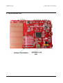
1
STM32-P407 development board
USER’S MANUAL
Initial release, February 2012
Designed by OLIMEX Ltd, 2011
All boards produced by Olimex LTD are ROHS compliant
OLIMEX© 2012
STM32-P407 User's Manual
Disclaimer:
© 2012 Olimex Ltd. Olimex®, logo and combinations thereof, are registered trademarks of Olimex Ltd.
Other terms and product names may be trademarks of others.
The information in this document is provided in connection with Olimex products. No license, express
or implied or otherwise, to any intellectual property right is granted by this document or in connection
with the sale of Olimex products.
Neither the whole nor any part of the information contained in or the product described in this document may
be adapted or reproduced in any material from except with the prior written permission of the copyright
holder.
The product described in this document is subject to continuous development and improvements. All
particulars of the product and its use contained in this document are given by OLIMEX in good faith.
However all warranties implied or expressed including but not limited to implied warranties of
merchantability or fitness for purpose are excluded. This document is intended only to assist the reader in the
use of the product. OLIMEX Ltd. shall not be liable for any loss or damage arising from the use of any
information in this document or any error or omission in such information or any incorrect use of the
product.
Thank you for purchasing STM32-P407 development board assembled by
OLIMEX LTD
Page 2 of 32
OLIMEX© 2012
STM32-P407 User's Manual
Table of Contents
CHAPTER 1.................................................................................................................5
OVERVIEW.................................................................................................................5
1. Introduction to the chapter.......................................................................................................5
1.1 Features.....................................................................................................................................5
1.2 Organization.............................................................................................................................6
CHAPTER 2 ................................................................................................................7
SETTING UP THE STM32-P407 BOARD...............................................................7
2. Introduction to the chapter.......................................................................................................7
2.1 Electrostatic warning...............................................................................................................7
2.2 Requirements...........................................................................................................................7
2.3 Powering the board..................................................................................................................8
2.4 Prebuilt software......................................................................................................................8
CHAPTER 3.................................................................................................................9
STM32-P407 BOARD DESCRIPTION.....................................................................9
3. Introduction to the chapter.......................................................................................................9
3.1 Layout (top view).....................................................................................................................9
3.2 Layout (bottom view).............................................................................................................10
CHAPTER 4...............................................................................................................11
THE STM32F407ZGT6 MICROCONTROLLER.................................................11
4. Introduction to the chapter.....................................................................................................11
4.1 The microcontroller...............................................................................................................11
CONTROL CIRCUITY............................................................................................13
5. Introduction to the chapter.....................................................................................................13
5.1 Reset........................................................................................................................................13
5.2 Clock.......................................................................................................................................13
CHAPTER 6...............................................................................................................14
HARDWARE.............................................................................................................14
6. Introduction to the chapter.....................................................................................................14
6.1 JTAG connector.....................................................................................................................14
6.2 UEXT......................................................................................................................................15
6.3 Pads on the proto area...........................................................................................................16
6.4 USB_OTG...............................................................................................................................17
6.5 USB HOST..............................................................................................................................18
6.6 LAN connector.......................................................................................................................18
6.7 PWR Jack...............................................................................................................................19
Page 3 of 32
OLIMEX© 2012
STM32-P407 User's Manual
6.8 Headphones connector..........................................................................................................19
6.9 SD/MMC slot..........................................................................................................................19
6.10 RS232_1................................................................................................................................20
6.11 RS232_2................................................................................................................................20
6.12 CAN connector.....................................................................................................................21
6.13 Battery connector.................................................................................................................22
6.14 Jumper description..............................................................................................................22
6.15 LCD Display with backlight................................................................................................25
6.16 VGA Color Camera.............................................................................................................25
6.17 Additional hardware components......................................................................................26
CHAPTER 7...............................................................................................................27
MEMORY..................................................................................................................27
7. Introduction to the chapter.....................................................................................................27
7.1 Memory map..........................................................................................................................28
CHAPTER 8...............................................................................................................29
SCHEMATICS..........................................................................................................29
8. Introduction to the chapter.....................................................................................................29
8.1 Eagle schematic......................................................................................................................29
8.2 Physical dimensions...............................................................................................................31
CHAPTER 9...............................................................................................................32
REVISION HISTORY..............................................................................................32
9. Introduction to the chapter.....................................................................................................32
9.1 Document revision.................................................................................................................32
9.2 Web page of your device.......................................................................................................32
Page 4 of 32
OLIMEX© 2012
STM32-P407 User's Manual
CHAPTER 1
OVERVIEW
1. Introduction to the chapter
Thank you for choosing the STM32-P407 development board from Olimex! This document
provides a User’s Guide for the Olimex STM32-P407 development board. As an overview, this
chapter gives the scope of this document and lists the board’s features. The document’s
organization is then detailed.
The STM32-P407 development board enables code development of applications running on the M4
CORTEX STM32F407ZGT6 microcontroller, manufactured by STMicroelectronics.
1.1 Features
•
STM32F407ZGT6 Cortex-M4 210DMIPS, 1MB Flash, 196KB RAM, 3×12-bit 2.4 MSPS
A/D, 2×12-bit D/A converters, USB OTG HS and USB OTG HS, Ethernet, 14 timers, 3 SPI,
3 I2C, Ethernet, 2 CANs, 3 12 bit ADCs, 2 12 bit DACs, 114 GPIOs, Camera interface
JTAG connector with ARM 2x10 pin layout for programming/debugging
•
•
512 KB fast external SRAM on board
4 Status LEDs
•
•
Stereo Audio Codec CS4344
CAN driver
•
•
Temperature sensor
Trimmer potentiometer
•
•
Joystick for navigation
6610 LCD color 128x128 pixel TFT display
•
•
SAMSUNG E700 VGA camera 640x480 color
Tamper and Wakeup buttons
•
•
2 RS232 drivers and connectors
25 Mhz quartz crystal
•
•
USB_OTG
USB_HOST
•
•
100 Mbit Ethernet
Mini SD/MMC card connector
•
Page 5 of 32
OLIMEX© 2012
STM32-P407 User's Manual
•
•
UEXT connector
Power Jack
•
•
RESET button and circuit
Power-on led
•
•
3V battery connector
Extension port connectors for many of microcontrollers pins
•
•
PCB: FR-4, 1.5 mm (0,062"), soldermask, silkscreen component print
Dimensions: 160x116 mm (6.3x4.6")
1.2 Organization
Each section in this document covers a separate topic, organized as follow:
–
–
Chapter 1 is an overview of the board usage and features
Chapter 2 provides a guide for quickly setting up the board
–
–
Chapter 3 contains the general board diagram and layout
Chapter 4 describes the component that is the heart of the board: the STM32F407ZGT6
microcontroller
–
–
Chapter 5 is an explanation of the control circuitry associated with the microcontroller to
reset. Also shows the clocks on the board
Chapter 6 covers the connector pinout, peripherals and jumper description
–
–
Chapter 7 shows the memory map
Chapter 8 provides the schematics
–
Chapter 9 contains the revision history
Page 6 of 32
OLIMEX© 2012
STM32-P407 User's Manual
CHAPTER 2
SETTING UP THE STM32-P407 BOARD
2. Introduction to the chapter
This section helps you set up the STM32-P407 development board for the first time.
Please consider first the electrostatic warning to avoid damaging the board, then discover the
hardware and software required to operate the board.
The procedure to power up the board is given, and a description of the default board behavior is
detailed.
2.1 Electrostatic warning
STM32-P407 is shipped in a protective anti-static package. The board must not be exposed to high
electrostatic potentials. A grounding strap or similar protective device should be worn when
handling the board. Avoid touching the component pins or any other metallic element.
2.2 Requirements
In order to set up the STM32-P407, the following items are required:
- 5 Vdc Power supply (or JTAG or SWD, or 5V TRACE, or 5V CAN, or 5V_USB, depending on
PWR_SEL jumper position)
- SWD interface programmer
Note: additionally, the board can be programmed via JTAG interface but there are signals
multiplexed with the LCD and the audio, so if using JTAG interface for programming you might
need to implement a software mechanism to stop them or you might not be able to reprogram again.
You may use a pair of the following devices for this purpose:
- Any of Olimex’s ARM-JTAG programmer/debuuger (keeping in mind the note above)
- Any of Olimex's ARM-JTAG programmer/debugger + ARM-JTAG-SWD + Rowley CrossWorks
Also, a host-based software toolchain is required in order to program/debug the STM32-P407
board. There are also a number of ready IDEs available like IAR Embedded Workbench, Rowley
CrossWorks, etc.
At the moment of writing this guide our ARM programmers/debuggers equipped with an ARMPage 7 of 32
OLIMEX© 2012
STM32-P407 User's Manual
JTAG-SWD work fine (out-of-the-box) with Rowley CrossWorks.
2.3 Powering the board
Provide +5 V DC to the board's power jack, OR +5 V via the JTAG or TRACE connector (before
providing the power set the PWR_SEL jumper in the correct position)
On powering the board the PWR LED, the SATA4 LED and the display should turn on. The
SATA1, SATA2 and SATA3 LEDs must start blinking consecutively.
If measuring the current consumption it should be around 30 mA.
2.4 Prebuilt software
On arrival the board has a basic demo installed which features test of the LEDs, the LCD, the
joystick, the camera.
IMPORTANT: If you have only a programmer with JTAG interface and you need to turn off the
peripherals using the JTAG signals press WKUP button! Pressing WKUP button will turn of those
modules and will allow JTAG reprogramming.
Page 8 of 32
OLIMEX© 2012
STM32-P407 User's Manual
CHAPTER 3
STM32-P407 BOARD DESCRIPTION
3. Introduction to the chapter
Here you get acquainted with the main parts of the board. Note the names used on the board differ
from the names used to describe them. For the actual names check the STM32-P407 board itself.
3.1 Layout (top view)
Page 9 of 32
OLIMEX© 2012
STM32-P407 User's Manual
3.2 Layout (bottom view)
Page 10 of 32
OLIMEX© 2012
STM32-P407 User's Manual
CHAPTER 4
THE STM32F407ZGT6 MICROCONTROLLER
4. Introduction to the chapter
In this chapter is located the information about the heart of STM32-P407 – its microcontroller. The
information is a modified version of the datasheet provided by its manufacturers.
4.1 The microcontroller
•Core: ARM 32-bit Cortex™-M4 CPU with FPU, Adaptive real-time accelerator (ART
Accelerator™) allowing 0-wait state execution from Flash memory, frequency up to 168 MHz,
memory protection unit, 210 DMIPS/1.25 DMIPS/MHz (Dhrystone 2.1), and DSP instructions
•Memories
•1 Mbyte of Flash memory
•192+4 Kbytes of SRAM including 64-Kbyte of CCM (core coupled memory) data RAM
•Flexible static memory controller supporting Compact Flash, SRAM, PSRAM, NOR and
NAND memories
•LCD parallel interface, 8080/6800 modes
•Clock, reset and supply management
•1.8 V to 3.6 V application supply and I/Os
•POR, PDR, PVD and BOR
•4-to-26 MHz crystal oscillator
•Internal 16 MHz factory-trimmed RC (1% accuracy)
•32 kHz oscillator for RTC with calibration
•Internal 32 kHz RC with calibration
•Sleep, Stop and Standby modes
•VBATsupply for RTC, 20×32 bit backup registers + optional 4 KB backup SRAM
•3×12-bit, 2.4 MSPS A/D converters: 24 channels and 7.2 MSPS in triple interleaved mode
•2×12-bit D/A converters
•General-purpose DMA: 16-stream DMA controller with FIFOs and burst support
•Up to 17 timers: up to twelve 16-bit and two 32-bit timers up to 168 MHz, each with up to 4
IC/OC/PWM or pulse counter and quadrature (incremental) encoder input
•Debug mode
•Serial wire debug (SWD) & JTAG interfaces
Page 11 of 32
OLIMEX© 2012
STM32-P407 User's Manual
•Cortex-M4 Embedded Trace Macrocell™
•Up to 114 I/O ports with interrupt capability
•Up to 15 communication interfaces
•3 × I2C interfaces (SMBus/PMBus)
•4 USARTs/2 UARTs (10.5 Mbit/s, ISO 7816 interface, LIN, IrDA, modem control)
•3 SPIs (37.5 Mbits/s), 2 with muxed full-duplex I2S to achieve audio class accuracy via
internal audio PLL or external clock
•2 × CAN interfaces (2.0B Active)
•SDIO interface
•Advanced connectivity
•USB 2.0 full-speed device/host/OTG controller with on-chip PHY
•USB 2.0 high-speed/full-speed device/host/OTG controller with dedicated DMA, on-chip
full-speed PHY and ULPI
•10/100 Ethernet MAC with dedicated DMA: supports IEEE 1588v2 hardware, MII/RMII
•8- to 14-bit parallel camera interface up to 54 Mbytes/s
•True random number generator
•CRC calculation unit
•96-bit unique ID
•RTC: subsecond accuracy, hardware calendar
For comprehensive information on the microcontroller visit the Microchip’s web page for a
datasheet.
At the moment of writing the microcontroller datasheet can be found at the following link:
http://www.st.com/internet/com/TECHNICAL_RESOURCES/TECHNICAL_LITERATURE/DAT
ASHEET/DM00037051.pdf
If the Cortex M4 processor listed above seems like an overkill we have the same board offered with
Cortex M3 one – STM32F207ZET6. The name of the board is STM32-P207. The table of
comparison can be found below:
STM32F207ZET6
STM32F407ZGT6
Maximum speed
120Mhz
168Mhz
Program memory
512KB
1024KB
Ram memory
132KB
192KB
Page 12 of 32
OLIMEX© 2012
STM32-P407 User's Manual
CHAPTER 5
CONTROL CIRCUITY
5. Introduction to the chapter
Here you can find information about reset circuit and quartz crystal locations.
5.1 Reset
STM32-P407 reset circuit includes R65 (10 KΩ), R66(560 Ω), C45(100 nF), STM32F407ZGT6 pin
25 (NRST) and a RESET button. The RESET is also connected to the proto area.
5.2 Clock
25 MHz quartz crystal Q1 is connected to pins 23 and 24 of the processor.
Real time clock (RTC) Q2 is found at pins 8 and 9 of the processor.
Page 13 of 32
OLIMEX© 2012
STM32-P407 User's Manual
CHAPTER 6
HARDWARE
6. Introduction to the chapter
In this chapter are presented the connectors that can be found on the board all together with their
pinout. Proto area is shown. Jumpers functions are described. Notes and info on specific peripherals
are presented. Notes regarding the interfaces are given.
6.1 JTAG connector
The 20 pin JTAG connector provides the interface for JTAG or/and SWD/TRACE
programming/debugging. It is advisable to use SWD/TRACE interface programmers.
JTAG/SWD interface
Pin #
Signal Name
Pin #
Signal Name
1
+3.3V
11
+3.3 V
2
+3.3V
12
GND
3
TRST/SPI1_MISO
13
TDO/I2S3_CK
4
GND
14
GND
5
PGCTDI/I2S3_WS
15
RST
6
GND
16
GND
7
TMS
17
+5V_J-LINK
8
GND
18
GND
9
TCK
19
+5V_J-LINK
10
GND
20
GND
Page 14 of 32
OLIMEX© 2012
STM32-P407 User's Manual
TRACE interface
Pin #
Signal Name
Pin #
Signal Name
1
+3.3V
11
+5V_TRACE
2
TMS
12
TEMP_ALERT
3
GND
13
+5V_TRACE
4
TCK
14
USB_HS_VBUSON
5
GND
15
GND
6
TDO/I2S3_CK
16
DCMI_D4
7
Not connected
17
GND
8
TDI/I2S3_WS
18
DCMI_D6
9
GND
19
GND
10
RST
20
DCMI_D7
6.2 UEXT
STM32-P407 board has UEXT connector and can interface Olimex's UEXT modules.
For more information on UEXT please visit:
http://www.olimex.com/dev/OTHER/UEXT.pdf
Pin #
Signal Name
1
+3.3V
2
GND
3
DCMI_D0/USART6_TX
4
USART6_RX
Page 15 of 32
OLIMEX© 2012
STM32-P407 User's Manual
5
SOFTWARE SCL
6
SOFTWARE SDA
7
SD_D3/USART3_RX/SPI3_MISO
8
SD_CLK/SPI3_MOSI
9
SD_D2/USART3_TX/SPI3_SCK
10
STAT3/CS_UEXT
6.3 Pads on the proto area
For your convenience the pads are named individually near each of them. Please take extra care
about the numbering but consider that there might be offset.
PAD #
Signal Name
PAD#
Signal Name
PA0
BUT WKUP
RST
RST
PA4
DCMI_HSYNC
PG0
A10
PA5
SPI1_SCK
PG1
A11
PA6
DCMI_PIXCLK
PG2
A12
PA8
MCO1
PG3
A13
PA9
OTG_FS_VBUS
PG4
A14
PA10
DCMI_D1
PG5
A15
PB0
LCD_BL
PG6
RIGHT(JOYSTICK)
PB1
BUZ
PG9
USART6_RX
PB2
CAM_ENB
PG10
SOFT_SCL
PB5
I2S3_SD
PF15
A9
PB9
CAN1_TX
PF14
A8
PB10
USB_FS_FAULT
PF13
A7
PB12
OTG_HS_ID
PF12
A6
PB13
OTG_HS_VBUS
PF11
CAM_RST
Page 16 of 32
OLIMEX© 2012
STM32-P407 User's Manual
PC5
ETH_RMII_RXD1
PF10
ETH_RXER
PC13
BUT TAMPER
PF9
SSTAT4/CAM_PWR
PD6
LCD_CS
PF8
STAT3/CS_UEXT
PE0
/BLE
PF7
STAT2/CAN_CTRL
PE1
/BHE
PF6
STAT1
PE2
TEMP_ALERT
PF5
A5
PE3
USB_HS_VBUSON
PF4
A4
PE4
DCMI_D4
PF3
A3
PE5
DCMI_D6
PF2
A2
PE6
DCMI_D7
PF1
A1
PE7
D4
PF0
A0
PE8
D5
PE15
D12
PE9
D6
PE14
D11
PE10
D7
PE13
D10
PE11
D8
PE12
D9
+5V
+5V DC
VBAT
VBAT
6.4 USB_OTG
Pin #
Signal Name
1
+5V
2
D-
3
D+
4
OTG_HS_ID
5
GND
Page 17 of 32
OLIMEX© 2012
STM32-P407 User's Manual
6.5 USB HOST
PIN#
SIGNAL NAME
1
+5 V
2
USB_HOST_D-
3
USB_HOST_D+
4
GND
6.6 LAN connector
PIN#
SIGNAL NAME
1
TX+
2
TX-
3
VDD
4
NOT CONNECTED
5
NOT CONNECTED
6
VDD
7
RX+
8
RX-
LED
Color
Usage
Right
Green
Link status
Left
Yellow
Activity status
Page 18 of 32
OLIMEX© 2012
STM32-P407 User's Manual
6.7 PWR Jack
Pin #
Signal Name
1
Power Input
2
GND
6.8 Headphones connector
6.9 SD/MMC slot
Pin #
Signal Name
1
DAT2
2
DAT3/CS
3
CMD/DI
4
VDD
5
CLK/SCLK
Page 19 of 32
OLIMEX© 2012
STM32-P407 User's Manual
6
VSS
7
DAT0/DO
8
DAT1
6.10 RS232_1
RS232_1 is located on USART6/SPI3 line. Check the jumper configuration.
Pin #
Signal Name
1
Not Connected
2
T1OUT
3
R1IN
4
Not Connected
5
GND
6
Not Connected
7
CTS
8
RTS
9
Not Connected
6.11 RS232_2
RS232_2 is located on USART3 (processor pins D13 – D14, A17 – A16)
Pin #
1
Signal Name
Not connected
Page 20 of 32
OLIMEX© 2012
STM32-P407 User's Manual
2
T1OUT
3
R1IN
4
Not connected
5
GND
6
Not connected
7
CTS
8
RTS
9
Not connected
6.12 CAN connector
Pin#
Signal name
1
Not connected
2
CANL
3
VSS
4
Not connected
5
VSS
6
GND
7
CANH
8
Not connected
9
+5V_CAN
Page 21 of 32
OLIMEX© 2012
STM32-P407 User's Manual
6.13 Battery connector
Pin #
Signal Name
1
VBAT
2
GND
6.14 Jumper description
Most of the jumper configurations are printed with white print on the PCB for your convenience.
PWR_SEL
On the setting of this jumper depends the way we power the board. There is a table printed on the
board with the positions. You can check the table below also. Position 1-2 is the one at the PWR
connector side.
PWR_SEL
1-2
+5V_EXT
3-4
+5V_J-LINK
5-6
+5V_CAN
7-8
+5V_USB_OTG
9 - 10
+5V_TRACE
Default position is 3-4.
Page 22 of 32
OLIMEX© 2012
STM32-P407 User's Manual
STAT1_E, STAT2_E, STAT3_E, STAT4_E
Those 4 jumpers control whether the LEDs are powered(closed) or not(open).
Default state is closed.
BOOT0_E
Connected to pin 138 (BOOT0/VPP), enables boot if closed.
Default state is open.
RST_E
Controls the RST on the RS232_1. If closed is present. Default state is not present.
Default state is open.
B1_1/B1_0, B0_1/B0_0
These jumpers should be moved together and control the camera being powered.
Default state is B1_0, B0_0 (camera powered).
Page 23 of 32
OLIMEX© 2012
STM32-P407 User's Manual
3.3V_MCU_EN
When closed enables the power supply on the STM32F207ZET.
Default state is closed.
TX_BOOT_E
If closed separates USART6_TX and PC10.
Default state is open.
RX_BOOT_E
If closed separates USART6_RX and PC11.
Default state is open.
3.3V_E
Board's digital power supply is disabled if open.
Enabled if closed.
Default state is open.
AGND_E
Page 24 of 32
OLIMEX© 2012
STM32-P407 User's Manual
Analog GND is disabled if open.
If closed Analog GND is enabled.
Default state is closed.
R-T
RST and TRST are separated if open.
RST and TRST are connected if closed.
Refer to the schematic near the JTAG connector for how this jumper influences the JTAG
programming of the board.
Default state is open.
CAN_T
Can termination is disabled if open.
Default state is open.
6.15 LCD Display with backlight
replica of Nokia 6610 color display 128x128 pixels
6.16 VGA Color Camera
640x480 pixels (0.3 mega pixel) Samsung 700 camera + connector
Page 25 of 32
OLIMEX© 2012
STM32-P407 User's Manual
6.17 Additional hardware components
The components below are mounted on STM32-P407 but are not discussed above. They are listed
here for completeness:
Joystick
Temperature sensor
Audio out
Trimmer
Buzzer
Additional memory
2 buttons + RST button
4 status LEDs + PWR LED
Page 26 of 32
OLIMEX© 2012
STM32-P407 User's Manual
CHAPTER 7
MEMORY
7. Introduction to the chapter
On the next page you can find a memory map for this family of processors. It is strongly
recommended to refer to the original datasheet released by STMicroelectronics for one of higher
quality.
Page 27 of 32
OLIMEX© 2012
STM32-P407 User's Manual
7.1 Memory map
Page 28 of 32
OLIMEX© 2012
STM32-P407 User's Manual
CHAPTER 8
SCHEMATICS
8. Introduction to the chapter
In this chapter are located the schematics describing logically and physically STM32-P407.
8.1 Eagle schematic
STM32-P407 schematic is visible for reference here. You can also find them on the web page for
STM32-P407 at our site: http://www.olimex.com/dev/stm32-P407.html. They are located in
HARDWARE section.
The EAGLE schematic is situated on the next page for quicker reference.
Page 29 of 32
OLIMEX© 2012
STM32-P407 User's Manual
Page 30 of 32
OLIMEX© 2012
STM32-P407 User's Manual
8.2 Physical dimensions
Note that all dimensions are in inches.
Page 31 of 32
OLIMEX© 2012
STM32-P407 User's Manual
CHAPTER 9
REVISION HISTORY
9. Introduction to the chapter
In this chapter you will find the current and the previous version of the document you are reading.
Also the web-page for your device is listed. Be sure to check it after a purchase for the latest
available updates and examples.
9.1 Document revision
Revision
Changes
Modified
Pages
A
Initial Creation
All
9.2 Web page of your device
The web page you can visit for more info on your device is http://www.olimex.com/dev/stm32P407.html. There you can find more info and some examples.
ORDER CODES:
STM32-P407 - completely assembled and tested
ARM-USB-TINY - for custom programming/debugging
ARM-USB-TINY-H - for custom programming/debugging
USB-MINI-CABLE - USBmini to USB-A cable
ARM-JTAG-SWD – SWD adapter for our ARM-JTAG programmers
How to order?
You can order to us directly or by any of our distributors.
Check our webpage http://www.olimex.com/ for more info.
Page 32 of 32