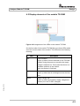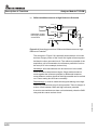
1
USER MANUAL
Analyzer Module
TS-PAM
User Manual
for ROHDE & SCHWARZ Analyzer Module TS-PAM
4th Issue / 11.05 / D 1152.3808.12
All rights, also translation into foreign languages, are reserved. No part of this manual is permitted
to be reproduced in any form (print, photocopy or any other method), also not for the preparation
of lectures, or processed, reproduced or made available using electronic systems without written
permission from ROHDE & SCHWARZ.
© The passing on to third parties and the reproduction of this documentation, utilisation and communication of its contents is not permitted unless specifically approved. Infringements will incur
claims for damages. All rights reserved in the case of the award of a patent or registration of a
design.
We draw to your attention that the names of software and hardware used in the User Manual, and
the brand names of the respective companies are, in general, the subject of protection as trademarks, or under proprietary rights, or patent law.
ROHDE & SCHWARZ GmbH & Co. KG
Corporate Headquarters
Mühldorfstr. 15
D-81671 München
Telephone:
Fax:
...49 (0)89/4129-13774
...49 (0)89/4129-13777
Printed in the Federal Republic of Germany. Errors excepted, subject to technical change without notice.
Safety Instructions
Attention!
Electrostatic
sensitive devices require
special care
Support Center
Telephone Europe:
+49 180 512 42 42
Telephone worldwide: +49 89 4129 13774
Fax:
+49 89 4129 13777
e-mail: [email protected]
If you have any technical queries about this Rohde &
Schwarz equipment, our Hotline at the Support Center of
Rohde & Schwarz Sales-GmbH will be glad to help.
Our team will discuss your queries and look for solutions to
your problems.
The Hotline is open Mondays to Fridays from 08.00 to 17.00
hrs.
For queries outside office hours, you can leave a message
or send a note via fax or email. We will then get back to you
as soon as possible.
Analyzer Module TS-PAM
Content
Content
1
Applications
1-1
1.1
General
1-1
1.2
Features of the TS-PAM
1-2
1.3
Features of the TS-PDC Module
1-3
2
View
2-1
3
Block Diagram
3-1
4
Design
4-1
4.1
Mechanical Design of the Module TS-PAM
4-1
4.2
Display elements of the module TS-PAM
4-3
4.3
Mechanical Design of TS-PDC
4-4
4.4
Display Elements of the Module TS-PDC
4-5
5
Description of Functions
5-1
5.1
Description of Functions of the Module TS-PAM
5-1
5.1.1
Acquisition Unit
5-1
5.1.2
Inputs and Measurement Ranges
5-2
5.1.3
Timing Control, Scanner
5-5
5.1.4
Synchronization, Trigger
5-5
5.1.5
Memory
5-6
5.1.6
Signal processing, Filter
5-7
5.1.7
Analog Bus Access
5-7
5.1.8
Measuring Functions
5-7
5.1.9
Particulars of Floating Measurements
5-8
5.1.10
Information for Operation with Dangerous Voltages
5-13
5.1.11
Power Supply
5-14
4th Issue 11.05
5.2
6
7
Description of Functions of the Module TS-PDC
5-15
Commissioning
6-1
6.1
Installation of the Plug-in Module
6-1
6.2
Installation of the Module TS-PDC
6-2
Software
7-1
7.1
7-1
Driver Software
1
Content
8
9
Analyzer Module TS-PAM
7.2
Soft Panel
7-2
7.3
Signal Analysis Library
7-4
7.4
Programming example TS-PAM
7-5
Self-test
8-1
8.1
LED Test
8-1
8.2
Power-on test
8-2
8.3
Self-test by the driver
8-2
Interface Description
9-1
9.1
Interface Description TS-PAM
9-1
9.1.1
Connector X1
9-1
9.1.2
Connector X20
9-2
9.1.3
Connector X10
9-3
9.1.4
Connector X30
9-5
9.2
Interface Description TS-PDC
9-6
9.2.1
9-6
10-1
4th Issue 11.05
10 Technical Data
Connector X20 (Extension Connector)
2
Analyzer Module TS-PAM
Figures
4th Issue 11.05
Figures
Figure 2-1
View of the TS-PAM ...........................................................................2-1
Figure 2-2
View of the Rear I/O Module TS-PDC ...............................................2-2
Figure 3-1
Block diagram of TS-PAM with TS-PDC in the CompactTSVP...... 3-1
Figure 3-2
Block diagram of Analyzer Module TS-PAM ...................................3-2
Figure 3-3
Block diagram of Rear I/O Module TS-PDC.....................................3-3
Figure 4-1
Arrangement of the connectors and LEDs on the module
TS-PAM ...............................................................................................4-1
Figure 4-2
Arrangement of the LEDs on the module TS-PAM .........................4-3
Figure 4-3
Arrangement of the connector and LEDs on the module TS-PDC 4-4
Figure 4-4
Arrangement of the LEDs on the module TS-PDC .........................4-5
Figure 5-1
Functional blocks of TS-PAM ...........................................................5-1
Figure 5-2
Signal inputs and scanner of an acquisition unit (path A) ............5-4
Figure 5-3
Trigger unit.........................................................................................5-6
Figure 5-4
Grounding procedure “Simple Single-ended Grounding” ............5-8
Figure 5-5
Grounding procedure “Single-ended, Grounding on Unit
under Test”.........................................................................................5-9
Figure 5-6
Grounding procedure “Floating with Potential as Reference” ...5-10
Figure 5-7
Grounding procedure “Differential Measurement with two
Channels”.........................................................................................5-11
Figure 5-8
Grounding procedure “Differential Measurement at High
Reference Potential” .......................................................................5-12
Figure 5-9
Permitted voltages on analog bus lines ........................................5-13
Figure 5-10
Block schematic diagram of Rear I/O Module TS-PDC ................5-15
Figure 7-1
Soft Panel TS-PAM ............................................................................7-2
Figure 7-2
Soft Panel TS-PAM switching...........................................................7-3
Figure 9-1
Connector X1 (view: plug side) ........................................................9-1
Figure 9-2
Connector X20 (view: plug side) ......................................................9-2
Figure 9-3
Connector X10 (view: front panel) ...................................................9-3
Figure 9-4
Connector X30 (view: plug side) ......................................................9-5
Figure 9-5
Connector X20 (view: plug side TS-PDC)........................................9-6
3
Analyzer Module TS-PAM
4th Issue 11.05
Figures
4
Analyzer Module TS-PAM
Tables
Tables
Features TS-PAM ...............................................................................1-2
Table 4-1
Connectors on the TS-PAM ..............................................................4-2
Table 4-2
Display elements on the module TS-PAM .......................................4-3
Table 4-3
Connector of the module TS-PDC....................................................4-4
Table 4-4
Display elements on the module TS-PDC .......................................4-5
Table 5-1
Measurement ranges.........................................................................5-3
Table 7-1
Driver installation TS-PAM................................................................7-1
Table 7-2
Installation of the signal analysis library ........................................7-4
Table 8-1
Statements about the LED Test........................................................8-1
Table 8-2
Statements about the power-on test................................................8-2
Table 9-1
Pin assignment for connector X1.....................................................9-1
Table 9-2
Pin assignment for connector X20...................................................9-2
Table 9-3
Pin assignment for connector X10 (view front panel).................... 9-3
Table 9-4
Pin assignment for connector X30...................................................9-5
Table 9-5
Pin assignment for connector X20 (TS-PDC)..................................9-6
4th Issue 11.05
Table 1-1
5
Analyzer Module TS-PAM
4th Issue 11.05
Tables
6
Analyzer Module TS-PAM
Applications
1 Applications
1.1 General
This manual describes the function and operation of the Analyzer
Module TS-PAM (wave form analyzer) for use in the Test System Versatile Platform CompactTSVP. The hardware is designed as a CompactPCI module which occupies only one slot in the front side of the
TSVP. The accompanying Rear I/O Module TS-PDC (DC/DC Transformer Module) is plugged into the same slot on the back side.
The following analyses are possible using the Analyzer Module
TS-PAM and the Signal Analysis Library:
•
Voltage and voltage changes with different qualifications
•
Time measurements
•
Events
•
Wave-form comparison
The wave form analyzer is able to record electrical signals on two
measuring paths (channels) at a high sampling rate of 20 MHz or on up
to eight measuring paths (channels) in the „Scan“operation (quasi simultaneous) at a the low sampling rate of 5 MHz. The signals can be
evaluated after acquisition with respect to parameters such as voltage,
time, frequency, events. The measurement options can, in many cases, replace a digital voltmeter (DVM), a timer/counter or a digital oscilloscope. The Analyzer Module TS-PAM covers the application range
above a fast sampling voltmeter (e.g. TS-PSAM or data acquisition
module with scanner).
4th Issue 11.05
A wide range of trigger options for acquisition of the correct measuring
interval and automatic analysis options in the actual production environment, where no optical evaluation of the signals can take place, ensure the reproducibility of the measurements.
The Test System Versatile Platform CompactTSVP TS-PCA3 allows
you to plug in measuring and control modules according to industry
standard CompactPCI or PXI. Apart from this, Rohde & Schwarz
modules use an expanded printed circuit board format and have access to a special analog measurement bus.
1-1
Applications
Analyzer Module TS-PAM
1.2 Features of the TS-PAM
Features TS-PAM
Two fully independent, floating acquisition units with working voltage
up to 125 VDC
Acquisition modes with up to 8 single-ended or 4 differential channels
High sampling rate 20 MSamples/s for two channels
Multi channel signal recording for up to 8 channels at 5 MSamples/s
Synchronous acquisition of 8 programable comparator signals and
PXI-trigger additionally
Wide dynamic range with 14 bit resolution
Input ranges ±0.2 VDC up to ±100 VDC ( 125 V max.))
3:1 relay multiplexer per channel
2 x 1 MSamples memory depth
Analog and digital trigger signals
Analog measurement bus access to 8 bus lines
Selftest capabilities
Soft front panel support for direct operation
LabWindows/CVI driver support
GTSL test software library in DLL format
4th Issue 11.05
Table 1-1 Features TS-PAM
1-2
Analyzer Module TS-PAM
Applications
1.3 Features of the TS-PDC Module
The Rear I/O Module TS-PDC is used as a floating DC voltage source
for the Analyzer Module TS-PAM . It contains two identical DC/DC converters. The following floating voltages are obtained from an input voltage of 5 VDC:
+15 VDC ±5%, 0.5A (2x)
–
-15 VDC ±5%, 0.5A (2x)
–
+5 VDC ±5%, 0.5A (2x)
–
+3.3 VDC ±5%, 0.25A (2x)
4th Issue 11.05
–
1-3
Analyzer Module TS-PAM
4th Issue 11.05
Applications
1-4
Analyzer Module TS-PAM
View
2 View
Figure 2-1 shows the Analyzer Module TS-PAM without the accompanying Rear I/O Module TS-PDC.
The Rear I/O Module TS-PDC is shown in Figure 2-2 .
4th Issue 11.05
Figure 2-1 View of the TS-PAM
2-1
View
Analyzer Module TS-PAM
4th Issue 11.05
Figure 2-2 View of the Rear I/O Module TS-PDC
2-2
Analyzer Module TS-PAM
Block Diagram
3 Block Diagram
Figure 3-1 shows the simplified functional block diagram of the
Analyzer Module TS-PAM and the Rear I/O Module TS-PDC in the
CompactTSVP .
Figure 3-2 shows the block diagram of the Analyzer Modules TS-PAM .
Figure 3-3 shows the block diagram of the Rear I/O Module TS-PDC.
4th Issue 11.05
Figure 3-1 Block diagram of TS-PAM with TS-PDC in the CompactTSVP
3-1
3-2
Figure 3-2 Block diagram of Analyzer Module TS-PAM
4th Issue 11.05
SRAM
Control Logic
(FPGA)
DC
I
S
O
L
A
T
I
O
N
I
S
O
L
A
T
I
O
N
DC
DC
Control
Logic
PLD
ADC
REF
Control
Logic
PLD
ADC
REF
Differential
cPCI
Interface
FPGA
Boot Loader
EEPROM
PLL
PXI_TRIG
8
PXI_CLK
GA
5
DC
Lo
Hi
Lo
Hi
Filter
400,100k,
Full BW
Filter
400,100k,
Full BW
Filter
400,100k,
Full BW
Filter
400,100k,
Full BW
Fast
Diff
Scan
2x
1:4
Fast
Diff
Scan
2x
1:4
Comp
DAC
Comp
DAC
Comp
DAC
Comp
DAC
REF
DAC
Comp
DAC
Comp
DAC
Comp
DAC
Comp
Gain
x1.6,x4
Gain
x1.6,x4
Gain
x1.6,x4
Gain
x1.6,x4
Gain
x1.6,x4
Gain
x1.6,x4
Gain
x1.6,x4
Gain
x1.6,x4
Attenuator
1,2,10,20,100,200
Attenuator
1,2,10,20,100,200
Attenuator
1,2,10,20,100,200
Attenuator
1,2,10,20,100,200
Attenuator
1,2,10,20,100,200
Attenuator
1,2,10,20,100,200
Attenuator
1,2,10,20,100,200
Attenuator
1,2,10,20,100,200
Hi
Hi
Hi
Hi
Hi
Hi
Hi
Hi
CHB_LO
CHA_LO
Input Multiplexer
GND
GND
Path A
Path B
REF
A1 A2 B1 B2 C1 C2 D1 D2
CHB_LO1
CHB4_HI1
CHB_HI2
CHB4_HI3
CHB3_HI1
CHB3_HI2
CHB3_HI3
CHB2_HI1
CHB2_HI2
CHB2_HI3
CHB1_HI1
CHB1_HI2
CHB1_HI3
CHA_LO1
CHA4_HI1
CHA4_HI2
CHA4_HI3
CHA3_HI1
CHA3_HI2
CHA3_HI3
CHA2_HI1
CHA2_HI2
CHA2_HI3
CHA1_HI1
CHA1_HI2
CHA1_HI3
LABA2
LABB2
LABC2
LABD2
GND
LABA1
LABC1
LABC1
LABD1
Block Diagram
Analyzer Module TS-PAM
Differential
+5 V
GND
Block Diagram
Regulator
1
+15 V
+5 V
+3.3 V
COM
-15 V
Regulator
2
+15 V
+5 V
+3.3 V
COM
-15 V
primary
DC-Transducer
ON/OFF
X 20
Analyzer Module TS-PAM
INHIBIT
4th Issue 11.05
Figure 3-3 Block diagram of Rear I/O Module TS-PDC
3-3
Analyzer Module TS-PAM
4th Issue 11.05
Block Diagram
3-4
Analyzer Module TS-PAM
Design
4 Design
4.1 Mechanical Design of the Module TS-PAM
The Analyzer Module TS-PAM is designed as a long cPCI plug-in
module for mounting in the front of the CompactTSVP. The insertion
depth is 300 mm. The board height of the module is 4 HU.
4th Issue 11.05
In order to ensure that it is inserted correctly into the CompactTSVP,
the front panel is furnished with a locating pin. The module is secured
in place with the two retaining screws on the front panel. Front connector X10 is used for connecting the UUTs. Connector X30 connects the
TS-PAM module to the analog bus backplane in the CompactTSVP.
The Connectors X20/X1 connect the TS-PAM module to the cPCI
backplane/PXI control backplane.
Figure 4-1 Arrangement of the connectors and LEDs on the module TS-PAM
4-1
Design
Analyzer Module TS-PAM
Name
Use
X1
cPCI connector
X10
Front connector
X20
cPCI connector
X30
Analog bus connector
4th Issue 11.05
Table 4-1 Connectors on the TS-PAM
4-2
Analyzer Module TS-PAM
Design
4.2 Display elements of the module TS-PAM
Figure 4-2 Arrangement of the LEDs on the module TS-PAM
On the front side of the module TS-PAM there are three LEDs which
show the current status of the module. The LEDs have the following
meaning:
4th Issue 11.05
LED
Description
red
Fault condition:
Lights up when a fault is detected on the TS-PAM
module during the power-on test after the supply
voltage is switched on. This means that there is a
hardware problem on the module.
(also see section 8: Self-test)
yellow
Communication:
Lights up when data is exchanged across the interface.
green
Supply voltage OK:
Lights up when all necessary supply voltages are
present (incl. the TS-PDC voltages).
Table 4-2 Display elements on the module TS-PAM
4-3
Design
Analyzer Module TS-PAM
4.3 Mechanical Design of TS-PDC
The module TS-PDC is a Rear I/O Module for insertion in the back side
of the CompactTSVP. The printed circuit board height of the module is
3 HU (134 mm). The module is attached with both fastening screws of
the front panel. The connector X20 connects the module TS-PDC with
the extension back panel in the CompactTSVP. The module TS-PDC
must always use the corresponding rear I/O slot for the main module
(e.g. module TS-PAM ).
WARNING!
The module TS-PDC must always be plugged into the corresponding rear I/O slot (same slot code) of the module TS-PAM .
If it is not correctly plugged in (e.g. cPCI/PXI standard modules
in the front area) both modules may be destroyed.
Figure 4-3 Arrangement of the connector and LEDs on the module TSPDC
X20
Use
Extension (Rear I/O)
Table 4-3 Connector of the module TS-PDC
4-4
4th Issue 11.05
Name
Analyzer Module TS-PAM
Design
4.4 Display Elements of the Module TS-PDC
Figure 4-4 Arrangement of the LEDs on the module TS-PDC
Eight light-emitting diodes (LEDs) are located on the front of the
TS-PDC module to show the current status of the generated supply
voltages. The individual LEDs have the following meanings:
LED
Description
1, lights up
+15 VDC (CHA), present
2, lights up
+5 VDC (CHA), present
3, lights up
+3.3 VDC (CHA), present
4, lights up
-15 VDC (CHA), present
5, lights up
+15 VDC (CHB), present
6, lights up
+5 VDC (CHB), present
7, lights up
+3.3 VDC (CHB), present
8, lights up
-15 VDC (CHB), present
4th Issue 11.05
Table 4-4 Display elements on the module TS-PDC
4-5
Analyzer Module TS-PAM
4th Issue 11.05
Design
4-6
Analyzer Module TS-PAM
Description of Functions
5 Description of Functions
5.1 Description of Functions of the Module TS-PAM
The Analyzer Module TS-PAM is a signal analyzer similar to a multichannel digital storage oscilloscope (DSO). It has two acquisition units,
which can be operated separately or synchronized. Thus, the TS-PAM
functions as two separate digital oscilloscopes or as a digital oscilloscope with twice the number of channels. The two acquisition units are
separated according to control/software as well as potential. Because
each path is floating, each path can be connected to a different potential and measured there with high accuracy of measurement. Naturally
the paths can also be grounded, as with digital oscilloscopes.
Path A
Acquisition Unit A
Attenuator/
Gain
Scanner
Filter
ADConverter
WaveformMemory
Trigger A
Sequence Control A
Trigger B
Sequence Control B
Path B
Attenuator/
Gain
Scanner
Filter
ADConverter
WaveformMemory
Acquisition Unit B
Figure 5-1 Functional blocks of TS-PAM
5.1.1 Acquisition Unit
4th Issue 11.05
Each acquisition unit has four channels with individually adjustable
gain.
In single-channel mode, two channels or one channel and the floating
reference potential can be statically selected. The A/D converter measures the difference signal with maximum sample rate. With two acquisition units, two signals with conversion rates up to 20 MHz can be recorded, which corresponds to a sampling period of 50 ns.
5-1
Description of Functions
Analyzer Module TS-PAM
In multi-channel mode, two to four signals of a path can be quasi-simultaneously acquired. The channels are scanned and recorded with time
offset. At the maximum sampling frequency of 20 MHz, the effective
sampling frequency for four aquisition channels is 5 MHz, the interval
delta time (offset) is 50 ns. You can select whether the difference between individual channels or the difference of the channels against the
floating reference potential is to be measured. With two acquisition
units, a total of eight channels can be simultaneously recorded.
Because in most cases, the floating potentials can serve as a reference
or even be measured single-ended against GND, all eight channels can
be used and there is seldom need to take the difference between two
channels. The reference potential of a path is connected to GND or different reference potential of the unit under test. With particularly sensitive units under test, it is possible that the test signal may be distorted
if the reference potential of a path is connected directly to the unit under
test (cause: The reference potential has a higher capacitance and higher leakage current to GND compared to an input). This can be avoided
by using two channels of a unit and measuring fully differential with two
high-impedance inputs.
In the standby state after software initialization, each acquisition unit is
connected to GND through a relay and a resistor, for reasons of signal
technology. During floating operation, this relay is automatically
opened when a connection is made to a front connector pin or to the
analog bus. During grounded operation, when the GND relay remains
closed, care must be taken that the relay and resistor are not overloaded.
Each measuring channel can be switched with relays to three input
channels, to four lines of the local analog bus LABxy, to the reference
potential CHA_LO or CHB_LO or to the analog output for the trigger
threshold of the comparator. If the local analog bus line is used as an
additional input, 4 x 8 = 32 pins on the connector X10 can be measured
without having to use a relay in the adapter or an additional plug-in
card.
If the local analog bus LAB is connected with the global analog bus AB,
up to eight channels can be simultaneously measured and there is access to an almost unlimited number of measuring points ( 90 channels
per plug-in module TS-PMB). Here too, single-ended and differential
measurements are possible.
5-2
4th Issue 11.05
5.1.2 Inputs and Measurement Ranges
Analyzer Module TS-PAM
Description of Functions
Each measuring channel has a programmable input divider and measurement amplifier. With nine measurement ranges from 0.2 V to 100 V,
small to high voltages can be optimally acquired with 14 bit resolution.
In the small measurement ranges, instead of the normal input impedance of 1 MΩ, higher impedances can be measured. Because the floating measuring technique is used, the measuring accuracy of the small
ranges is also possible for small signals on high potential.
The maximum permitted rated voltage between arbitrary pins is 125 V.
Measurement range
Resolution
Input impedance
± 100 V
15 mV
1 MΩ
± 50 V
7.5 mV
1 MΩ
± 20 V
3 mV
1 MΩ
± 10 V
1.5 mV
1 MΩ
±5V
0.75 mV
1 MΩ or >10 MΩ selectable
±2V
0.3 mV
1 MΩ or >10 MΩ selectable
±1V
0.15 mV
1 MΩ or >10 MΩ selectable
± 0.5 V
75 µV
1 MΩ or >10 MΩ selectable
± 0.2 V
30 µV
1 MΩ or >10 MΩ selectable
4th Issue 11.05
Table 5-1 Measurement ranges
5-3
Description of Functions
Analyzer Module TS-PAM
Analog Bus
a1 a2 b1 b2
Local
Analog Bus
Coupling Relays
LABa1
LABa2
LABb1
LABb2
relay cross point
=
Fast Scanner
c1 c2 d1 d2
LABc1
LABc2
LABd1
LABd2
Scope Channels
CHA1
Input Channels
CHA1_HI1
CHA1_HI2
CHA1_HI3
DAC
CHA2
CHA2_HI1
CHA2_HI2
CHA2_HI3
HI
ADC
DAC
CHA3
LO
CHA3_HI1
CHA3_HI2
CHA3_HI3
DAC
CHA4
CHA4_HI1
CHA4_HI2
CHA4_HI3
DAC
CHA_LO1
50
CHA_LO
GND
Figure 5-2 Signal inputs and scanner of an acquisition unit (path A)
The inputs are DC coupled. An AC coupling can be done by connecting
an external capacitor in series. The time constant is optimized by the
appropriate selection of R and C on the measuring frequency and the
desired transient time.
Four programmable analog sources (DAC) per acquisition unit set the
trigger threshold of the comparators of each channel and can be connected as a control voltage source for the self-test to the analog bus.
The programming is according to the value of the trigger threshold and
5-4
4th Issue 11.05
Signals can be recorded within the input bandwidth. Similarly to digital
oscilloscopes, no anti-aliasing filter is provided. For signal conditioning,
hardware low pass filters can be connected in series.
Analyzer Module TS-PAM
Description of Functions
the set measurement range.
5.1.3 Timing Control, Scanner
The sampling rate can be varied so that slow or fast signals are optimally acquired and stored in the wave form memory. Because the timing of each acquisition unit can be independently set, slow and fast signals can be simultaneously optimally acquired, which results in a considerably better use of the wave form memory and effectively increases
its depth.
Depending on whether the single-channel or multi-channel operating
mode is used, the sampling rate can be max. 20 MHz or 5 MHz.
The precise time reference is derived from the 10 MHz PXI clock of the
Test System Versatile Platform CompactTSVP.
5.1.4 Synchronization, Trigger
Each acquisition unit can be started through the software, through the
test signals, external trigger inputs or PXI trigger inputs (from other
modules). For triggering through the test signals, analog comparators
with programmable threshold and selectable flanks are used.
Trigger output signals can trigger other modules on the front connector
X10 or on the PXI trigger bus. Through the pins XTO1 and XTO2, the
trigger time points of both acquisition units or the eight analog trigger
signals can be fed out. These signals can also be fed to the eight PXI
trigger lines.
4th Issue 11.05
The acquisition units can begin the recording synchronously, independently or initiated by the other acquisition unit. The storage in the wave
form memory can be done pre- or post-trigger.
5-5
Description of Functions
Analyzer Module TS-PAM
Acquisition Unit A
Start/Stop
PXI Trigger 0...7
8
XTI 1,2
2
8
DLY
IT1_A
PXI 0...7
IT1_A
Analog Trigger
AT A1...B4
XTI 1
AT A1...B4
8
Software
IT1_A
IT1_B
AT A1...B4
XTI 1
XTI 2
XTO 1
2
8
DLY
IT1_B
IT1_B
XTI 2
AT A1...B4
XTO 2
Acquisition Unit B
Start/Stop
Figure 5-3 Trigger unit
The wave form memory contains 1 MSamples (of 32 Bit width) per
acquisition unit. This means that in the single-channel mode, two channels (each acquisition unit) can record a maximum of 1 MSamples
each. In the multi-channel mode, eight channels up to a depth of
256 ksamples each can be measured. In addition to the analog values,
the trigger information from the PXI-Bus and the analog comparators is
also recorded.
5-6
4th Issue 11.05
5.1.5 Memory
Analyzer Module TS-PAM
Description of Functions
5.1.6 Signal processing, Filter
The measuring channels are broadband and have, like digital oscilloscopes, no specific anti-aliasing filters. For noise suppression, a
100 kHz or 400 Hz filter can be connected in the path. It has to be observed that the filters are arranged behind the measuring scanner. The
filters only function correctly if the filter cut-off frequency is distinctly
higher than the scan frequency. Otherwise, a distortion of the measurement value can occur up to an identical test signal of all channels.
An additional filtering can be obtained with the digital filter (low pass filter with cut-off frequency 0.2 x sampling frequency).
Additional special filter features can be implemented with software by
processing of the waveform arrays with commercially available programs.
5.1.7 Analog Bus Access
Each input channel has direct access to four local analog bus lines and
through coupling relays to the global analog bus. Thus, a total of eight
channels can be simultaneously connected to the analog bus. Instead
of an input channel, the floating reference potential CHA_LO or
CHB_LO can be switched to the analog bus. In this way, the measuring
channels can measure signals from other switch modules, and signals
to the connector X10 can also be connected to other measuring modules.
When there is signal feed through the analog bus and other cards, it
must be noted that the best signal quality is obtained only for short signal paths. Signals to the connector X10 can therefore be best measured.
4th Issue 11.05
5.1.8 Measuring Functions
The acquisition units can record analog signals and at the same time
digital trigger signals within a given time. An analysis of the wave forms
can be done with the Signal Analysis Library (see Software Analysis Library in Section 7.3).
5-7
Description of Functions
Analyzer Module TS-PAM
5.1.9 Particulars of Floating Measurements
To make optimum use of the possibilities of floating measurement of
TS-PAM, it is important to look at the grounding. The unit under test or
the measuring instrument must be grounded in order to obtain reproducible, stable measuring results. Only with very slow measuring techniques (battery operated hand multimeters) the hum can be equalized
by decelerating averaging. For fast and accurate measurements, one
must give some thought to the grounding. It is important here to only
provide a single grounding point. See examples Figure 5-4 to
Figure 5-8 .
a)
Simple Single-ended Grounding
CHA1_HI
ADC
Single-ended,
separate GND
HI
LO
1
2
3
CHA1_HI2
60V
CHA_LO
CHA_LO1
DUT
50
Figure 5-4 Grounding procedure “Simple Single-ended Grounding”
In the simplest case (Figure 5-4 ) with low accuracy requirements,
grounding is done “somewhere”, i.e. the unit under test is grounded in the fixture, the measuring unit is internally connected to
GND.
Advantage: Only the test signals are considered; the grounding is
connected in some way. The connection becomes very simple. If
the signals are fed through the analog bus, you save one bus line
for the GND.
When there is a small difference in the grounding potentials, transient currents flow which distort the measurement. The LO input of
the measuring unit is not arbitrarily low resistant but connected to
ground through approx. 50 Ω; faults up to 50 mV can be caused by
derivative currents. This type of connection has the hidden danger
that one may inadvertently place a grounded voltage on CHA_LO.
Thus, there may be a higher current which destroys the relay con-
5-8
4th Issue 11.05
Disadvantage: Low accuracy, particularly for signals in the magnitude of 100 mV and lower.
Analyzer Module TS-PAM
Description of Functions
tacts. Therefore, there is here a PTC resistor with a approx. 50 Ω
resistance built in, which limits this current. However, it must be
ensured that neither the max. current of the GND relay (500 mA)
nor the switching power of 15 W are exceeded.
Measurement a) is used for digital oscilloscopes and non-differential A/D converter cards. There is no option to separate the acquisition unit from GND for these devices.
b)
Single-ended, Grounding on the Unit under Test
CHA1_HI
ADC
HI
LO
2
3
DUT
CHA_LO
Single-ended,
one common GND
at DUT
60V
CHA_LO1
50
Figure 5-5 Grounding procedure “Single-ended, Grounding on Unit under Test”
With this wiring (Figure 5-5), the floating character of the acquisition unit of TS-PAM is used to ground only on the low-resistance
ground point of the unit under test (grounding only on one point).
Advantage: Accurate measurements even at low voltages, no
ground loops or potential differences, because there is only a single ground point.
4th Issue 11.05
Disadvantage: The CHA_LO must be specifically connected with
relays and wired in the fixture. When there is signal feed through
the analog bus, an additional bus line is necessary.
5-9
Description of Functions
Analyzer Module TS-PAM
c)
Floating with Potential as Reference
CHA1_HI
ADC
HI
LO
1
2
3
CHA_LO
Floating,
CHA_LO
as reference
CHA_LO1
0.1 V
60V
50
Figure 5-6 Grounding procedure “Floating with Potential as Reference”
With this wiring, (Figure 5-6 ) the measuring unit can be operated
on a deviating, higher potential (instead of being grounded).
Advantage: Despite a voltage of 60 V e.g. , the smallest ranges
and not the 100-V range can be used to measure the current. The
common mode suppression is nearly ideal using the floating
measuring technique.
Disadvantage: The „cold“ connection CHA_LO is not exactly equal
to the „hot“ signal connection (CHA1_HI2). The LO connection has
a greater capacity (to the order of 1 nF) to ground and exhibits
greater leak currents between LO and GND. In most cases this capacity can change the signal on the unit under test. Therefore LO
must be applied to a low resistant point of the unit under test. In
the example of the current measurement by the voltage drop at a
resistor, this is the side facing the source.
4th Issue 11.05
Digital oscilloscopes and non-differential A/D converter cards
must use two channels for this. Otherwise, they can only measure
in the inaccurate large measurement ranges (60 V). Even differential A/D converter cards must use the large measurement ranges
and lose accuracy.
5-10
Analyzer Module TS-PAM
d)
Description of Functions
Differential measurement with two Channels
ADC
HI
CHA1_HI
LO
Differential,
floating, second
channel as reference
2
3
CHA1_HI2
0.1 V
60V
CHA2_HI
1
2
3
CHA2_HI1
CHA_LO
CHA_LO1
50
Figure 5-7 Grounding procedure “Differential Measurement with two
Channels”
Similarly to c), with this wiring (Figure 5-7 ), measurement can be
done on a different potential. However, a high-resistance separate
channel with low capacitance is used as reference.
For reproducible measurements the input ranges with 1 MΩ input
resistance must be used. This reistance must be selected specifically in the small measuring ranges.
Reason: Since the acquisition unit is operated here without direct
reference potential, leak currents of the operational amplifier cannot otherwise flow to the reference potential CHA_LO.
Advantage: The high-resistance input from CHA2_HI1 distorts the
signal on the unit under test very little. Measurement can be done
in the more accurate small measurement ranges.
4th Issue 11.05
Disadvantage: An additional channel is necessary.
5-11
Description of Functions
Analyzer Module TS-PAM
e)
Differential Measurement at High Reference Potential
ADC
HI
CHA1_HI
LO
Differential, floating,
DUT high potential
as reference
CHA2_HI
1
2
3
1
2
3
+5V
-5V
60V
CHA_LO
CHA_LO1
50
Figure 5-8 Grounding procedure “Differential Measurement at High
Reference Potential”
The wiring as in Figure 5-8 is optimally suited when a unit under
test has a larger portion of the circuit at a higher reference potential than the other grounded circuit. The reference potential of the
acquisition unit is connected to the reference potential of unit under test (60 V in the example, broken line).
Advantage: All measurements can be carried out in the small,
more accurate measurement ranges. Single-ended measurements against the reference potential or differential measurements between various signals of the high potential can be carried
out. Fewer analog bus lines are necessary.
Disadvantage: It must be noted which signals belong to the high
reference potential and a line for this provided. There is danger of
a short circuit between GND and high reference potential.
4th Issue 11.05
It must be ensured that one does not inadvertantly close the GND
relay and thus cause a short circuit.
5-12
Analyzer Module TS-PAM
Description of Functions
5.1.10 Information for Operation with Dangerous Voltages
The following voltages are considered “dangerous live” under
EN 61010-1.
•
70 V DC
•
33 V AC eff
•
46.7 V AC peak
CAUTION!
When operating the Analyzer Module TS-PAM above these voltage limits, the instructions under EN 61010-1 must be followed.
The Analyzer Module TS-PAM and the Test System Versatile Platform
CompactTSVP are designed for a maximum voltage of 125 V between
floating measuring components, analog buses and GND. It must be
ensured that this limit is not exceeded at any time, even at summation
of the voltages, even through alternating signals.
Figure 5-9 shows some typical permissible voltage configurations
between analog buses and ground.
0...125 V
Analog
bus
0...125 V
- 125 V
5V
125 V
125 V max
125 V max
125 V max
floating
125 V max!!
125 V max!!
0...125 V
125 V max!!
120 V
125 V max!!
125 V
GND referenced
signals
Figure 5-9 Permitted voltages on analog bus lines
4th Issue 11.05
For reasons of fire safety, it is recommended in EN 61010-1 that for
DC-sources, the current or the rating be limited to 150 VA.
5-13
Description of Functions
Analyzer Module TS-PAM
5.1.11 Power Supply
4th Issue 11.05
The digital portion of the Analyzer Module TS-PAM is supplied with
power of +5 V and +3.3 V of the CompactPCI Bus. The two floating
measuring portions are each supplied with a set of floating voltages,
+5 V, +3.3 V, +15 V, -15 V from the rear I/O module TS-PDC (DC/DC
converter). The associated capacity is taken from the 5-V-CompactPCI
supply.
5-14
Analyzer Module TS-PAM
Description of Functions
5.2 Description of Functions of the Module TS-PDC
The Rear I/O Module TS-PDC is configured as a primary reference
DC/DC converter. The input voltage (5 VDC) is transfered to two secondary potentials and rectified to the nominal voltage by line controllers. The status of the output voltage is displayed in each case by an
LED.
–
+15 VDC, 0.5A (2x)
–
-15 VDC, 0.5A (2x)
–
+5 VDC, 0.5A (2x)
–
+3.3 VDC, 0.25A (2x)
+5 V
GND
ON/OFF
Regulator
1
+15 V
+5 V
+3.3 V
COM
-15 V
Regulator
2
+15 V
+5 V
+3.3 V
COM
-15 V
primary
DC-Transducer
X 20
The following DC voltages are generated:
INHIBIT
4th Issue 11.05
Figure 5-10 Block schematic diagram of Rear I/O Module TS-PDC
5-15
Analyzer Module TS-PAM
4th Issue 11.05
Description of Functions
5-16
Analyzer Module TS-PAM
Commissioning
6 Commissioning
6.1 Installation of the Plug-in Module
•
Power down and switch off the CompactTSVP.
•
Select a suitable front slot (slots 5-15 possible).
•
Remove the corresponding front panel portion from the TSVP
chassis by loosening the two screws.
WARNING!
Check the backplane connectors for bent pins! Any bent pins
must be straightened!
Failure to do this may permanently damage the backplane!
•
Apply moderate pressure to insert the plug-in module (use locating
pin to attach).
WARNING!
To insert the plug-in module, use both hands to guide carefully
into the backplane connectors.
•
The module is correctly located when a distinct “stop” can be felt.
•
Tighten the two retaining screws on the front panel of the module.
WARNING!
4th Issue 11.05
Install the associated TS-PDC rear I/O module as described in
Section 6.2 .
6-1
Commissioning
Analyzer Module TS-PAM
6.2 Installation of the Module TS-PDC
To install the plug-in module, proceed as follows:
•
The TS-PAM module must have been installed beforehand.
•
Select the corresponding rear I/O slot for the TS-PAM module.
•
Remove the corresponding rear panel portion from the CompactTSVP chassis by loosening the two screws.
WARNING!
Check the backplane connectors for bent pins! Any bent pins
must be straightened!
Failure to do this may permanently damage the backplane!
•
Push in the plug-in module using moderate pressure.
WARNING!
To insert the plug-in module, use both hands to guide carefully
into the backplane connectors.
The module is correctly located when a distinct “stop” can be felt.
•
Tighten the two retaining screws on the front panel of the module.
4th Issue 11.05
•
6-2
Analyzer Module TS-PAM
Software
7 Software
7.1 Driver Software
For the functions of the signal recording of the Analyzer Module
TS-PAM , a LabWindows IVI SCOPE driver is available. All other functions of the hardware are served by specific extensions of the driver.
The driver is a component of the ROHDE & SCHWARZ GTSL software. All functions of the driver are fully documented in the online help
and in the LabWindows/CVI Function Panels.
During driver installation, the following software modules are installed:
Module
Path
Comment
rspam.dll
<GTSL directory>\Bin
Driver
rspam.hlp
<GTSL directory>\Bin
Help file
rspam.fp
<GTSL directory>\Bin
LabWindows CVI Function Panel file,
function panels for CVI development interface
rspam.sub
<GTSL directory>\Bin
LabWindows CVI attribute file. This file is
required by some „function panels“.
rspam.lib
<GTSL directory>\Bin
Import Library
rspam.h
<GTSL directory>\Include
Header file for the driver
Table 7-1 Driver installation TS-PAM
NOTE:
4th Issue 11.05
To use the driver, the IVI and VISA libraries from National Instruments are necessary.
7-1
Software
Analyzer Module TS-PAM
7.2 Soft Panel
For the Analyzer Module TS-PAM, there is a Soft Panel available
(Figure 7-1 ). The Soft Panel is based on the LabWindows CVI driver.
The Software Panel enables interactive operation of the module. The
measured values are displayed graphically.
4th Issue 11.05
Figure 7-1 Soft Panel TS-PAM
7-2
Analyzer Module TS-PAM
Software
4th Issue 11.05
The switching of the signal path of TS-PAM can be done through the
Soft Panel (Figure 7-2 ).
Figure 7-2 Soft Panel TS-PAM switching
7-3
Software
Analyzer Module TS-PAM
7.3 Signal Analysis Library
The Signal Analysis Library offers functions for the analysis of the signals recorded by the Analyzer Module TS-PAM . The following signal
parameters can be determined:
•
Frequency, period
•
Average value, RMS
•
Rise and fall times
•
Pulse width
•
Maximum and minimum values (absolute and relative maxima/minima)
•
Event counting (slopes, minima, maxima)
•
Time measurement between two events
In addition, the Signal Analysis Library offers the following functions:
•
Wave form comparison
•
Calculation of reference wave forms
•
Loading and saving of the wave forms as files
•
Display of signal waves with reference curves and markers
Module
Path
Comment
siganl.dll
<GTSL directory>\Bin
Driver
siganl.hlp
<GTSL directory>\Bin
Help file
siganl.fp
<GTSL directory>\Bin
LabWindows CVI Function Panel file,
function panels for CVI development interface
siganl.lib
<GTSL directory>\Bin
Import Library
siganl.h
<GTSL directory>\Include
Header file for the driver
The analysis of audio signals is possible with the Audio Analysis Library
TS-LAA. This library offers the following functions:
7-4
•
RMS calculation
•
Single/Multitone frequency response
•
Distortion factor
•
Filter (low-pass, high-pass, band-pass, band-stop, CCIR weighted/unweighted)
4th Issue 11.05
Table 7-2 Installation of the signal analysis library
Analyzer Module TS-PAM
•
Software
Windowing of the signal
7.4 Programming example TS-PAM
The following sample program shows the recording of a signal which
contacts the connections CHA1_HI1 and CHA_LO1 on the front side
connector.
/*
This sample shows the acquisition of analog wave forms
using the TS-PAM module.
Error handling is not considered in this sample in order to
keep it easy to read. The return status should be checked for
VI_SUCCESS after each driver call.
*/
#include <ansi_c.h>
#include <userint.h>
#include "rspam.h"
int main (int argc, char *argv[])
{
ViSession vi;
ViStatus status;
ViReal64
ViInt32
ViReal64
ViReal64
* pWaveform = VI_NULL; /* pointer to wave form array */
actualPoints;
/* number of samples returned from */
initialX;
/* time of the first sample, relative
to the trigger event */
xIncrement;
/* time between two samples */
/*
Open a session to the device driver. The resource descriptor
depends on the slot number of the TS-PAM module and must be
adapted to the target system.
*/
status = rspam_InitWithOptions ( "PXI1::13::0::INSTR",
VI_TRUE,
VI_TRUE,
"Simulate=0,RangeCheck=1",
&vi);
/*
4th Issue 11.05
Configure the acquisition time base for path A:
Take a minimum of 20000 samples in 1 ms
- Sample frequency is 20 MHz
- Trigger delay = 0, i.e. no pre- or post-triggering
*/
status = rspam_ConfigureAcquisitionRecordPath (vi, RSPAM_VAL_PATH_A,
1.0e-3, 20000, 0.0);
/*
Configure channel CHA1 for a signal between -5 V and + 5 V.
The vertical range is 10 V (peak-to-peak), the offset is 0 V.
*/
status = rspam_ConfigureChannel (vi, "CHA1", 10.0, 0.0,
RSPAM_VAL_DC, 1.0, VI_TRUE);
/*
7-5
Software
Analyzer Module TS-PAM
Configure channel CHA1 for 1 MOhm impedance, no lowpass filter
*/
status = rspam_ConfigureChanCharacteristics (vi, "CHA1", 1.0e6, 20.0e6);
/*
Configure the trigger:
- Edge trigger
- Trigger level 2.5 V, positive slope
*/
status = rspam_ConfigureTriggerPath (vi ,RSPAM_VAL_PATH_A,
RSPAM_VAL_EDGE_TRIGGER );
status = rspam_ConfigureTriggerSourcePath (vi, RSPAM_VAL_PATH_A,
"CHA1", 2.5,
RSPAM_VAL_POSITIVE);
/*
Configure the path for floating acquisition
*/
status = rspam_ConfigureGroundPath (vi, RSPAM_VAL_PATH_A, VI_FALSE);
/*
Connect the instrument to the front connector
and wait until all relays have been closed
*/
status = rspam_Connect (vi, "CHA1_HI", "CHA1_HI1");
status = rspam_Connect (vi, "CHA_LO", "CHA_LO1");
status = rspam_WaitForDebounce ( vi, 1000 );
/*
Get the actual number of points for the acquisition and allocate
memory for it. Note that this value may be greater than the minimum
number of samples requested above.
*/
status = rspam_ActualRecordLengthPath (vi, RSPAM_VAL_PATH_A,
&actualPoints);
pWaveform = calloc (actualPoints, sizeof(ViReal64));
/*
Start the acquisition
- Timeout is 1000 ms
*/
status = rspam_ReadWaveform (vi, "CHA1", actualPoints, 1000,
pWaveform, &actualPoints, &initialX,
&xIncrement);
Display the wave form
*/
status = WaveformGraphPopup ("Waveform", pWaveform, actualPoints,
VAL_DOUBLE, 1.0, 0.0, initialX,
xIncrement);
/*
Close the driver session
*/
status = rspam_close ( vi );
/*
7-6
4th Issue 11.05
/*
Analyzer Module TS-PAM
Software
free memory
*/
free ( pWaveform );
return 0;
4th Issue 11.05
}
7-7
Analyzer Module TS-PAM
4th Issue 11.05
Software
7-8
Analyzer Module TS-PAM
Self-test
8 Self-test
The Analyzer Module TS-PAM has integrated self-test capability. The
following tests are possible:
•
LED Test
•
Power-on test
•
Self-test by the driver
8.1 LED Test
When the device is switched on, all three LEDs are lit for about one second. This indicates that the 5 V supply voltage is present and all LEDs
are working, also that the power-on test was successful. The following
statements can be made about the different LED statuses in this power-on phase:
LED
Description
One LED
does not light
up
Hardware problem on the module LED faulty
No LED's
light up
No +5V supply
Table 8-1 Statements about the LED Test
NOTE:
4th Issue 11.05
If diagnostics suggest a problem with the supply voltage, the
LEDs for the associated rear I/O module, TS-PDC, must be inspected visually. If a supply voltage failure is confirmed, the TSPDC module must be replaced.
8-1
Self-test
Analyzer Module TS-PAM
8.2 Power-on test
The power-on test runs at the same time as the LED test. In this test,
the result of the FPGA loading process is calculated. The following
statements can be made about the different statuses of the red and
green LEDs:
LED
Description
Green LED
on
all supply voltages present
green LED
off
at least one supply voltage from TS-PAM module or
the TS-PDC module is not present
red LED off
no errors were detected
red LED on
The FPGA/µP was not successfully loaded
Table 8-2 Statements about the power-on test
NOTE:
If diagnostics suggest a problem with the supply voltage, the
LEDs for the associated rear I/O module, TS-PDC, must be inspected visually. If a supply voltage failure is confirmed, the TSPDC module must be replaced.
8.3 Self-test by the driver
The driver which is supplied has a more extensive self-test. It is started
through the standard self-test function and delivers a “PASS” or “FAIL”
result.
In the TSVP self-test, a test report is generated.
NOTE:
4th Issue 11.05
Information on starting the self-test and on the sequence of the
necessary steps can be found in the GTSL software description
or the GTSL online help.
8-2
Analyzer Module TS-PAM
Interface Description
9 Interface Description
9.1 Interface Description TS-PAM
9.1.1 Connector X1
25
F E D C BAZ
4th Issue 11.05
Figure 9-1 Connector X1 (view: plug side)
Pin
F
25 GND
24 GND
23 GND
22 GND
21 GND
20 GND
19 GND
18 GND
17 GND
16 GND
15 GND
12..14
11 GND
10 GND
9 GND
8 GND
7 GND
6 GND
5 GND
4 GND
3 GND
2 GND
1 GND
E
D
C
B
A
5V
3.3V
ENUM#
REQ64#
5V
ACK64#
AD[0]
V(I/O)
5V
AD[1]
AD[2]
5V
AD[3]
AD[4]
3.3V
AD[5]
AD[6]
3.3V
GND
AD[7]
C/BE[0]#
M66EN
AD[8]
AD[9]
3.3V
AD[10]
AD[11]
V(I/O)
GND
AD[12]
AD[13]
GND
AD[14]
AD[15]
3.3V
C/BE[1]#
PAR
3.3V
GND
SERR#
PERR#
GND
IPMB_SDA
IPMB_SCL
3.3V
LOCK#
STOP#
V(I/O)
GND
DEVSEL#
TRDY#
BD_SEL#
IRDY#
FRAME#
3.3V
Key Area
C/BE[2]#
GND
AD[16]
AD[17]
AD[18]
AD[19]
AD[20]
3.3V
GND
AD[21]
AD[22]
GND
AD[23]
IDSEL
C/BE[3]#
AD[24]
AD[25]
V(I/O)
GND
AD[26]
AD[27]
GND
AD[28]
AD[29]
AD[30]
AD[31]
CLK
3.3V
GND
REQ#
GNT#
GND
RST#
BSRSV
BSRSV
INTS
INTP
V(I/O)
HEALTHY#
IPMB_PWR
INTD#
5V
INTC#
INTB#
INTA#
TDI
TDO
TMS
5V
TCK
5V
+12V
TRST#
-12V
5V
Z
GND
GND
GND
GND
GND
GND
GND X1
GND
GND C
GND O
GND N
N
GND E
GND C
GND T
GND O
GND R
GND
GND
GND
GND
GND
GND
Table 9-1 Pin assignment for connector X1
9-1
Interface Description
Analyzer Module TS-PAM
9.1.2 Connector X20
22
F E D C BAZ
Figure 9-2 Connector X20 (view: plug side)
NC = not connected, NP = not populated
F
GND
GND
GND
GND
GND
GND
GND
GND
E
D
C
GA0
GA1
GA2
A
GA3
GA4
GND
GND
GND
PXI_TRIG6
GND (CAN-En)
PXI_TRIG5
PXI_CLK10
PXI_TRIG7
GND
PXI_TRIG4
PXI_TRIG3
GND
PXI_TRIG2
PXI_TRIG0
PXI_TRIG1
GND
Z
GND
GND
GND
GND
GND
GND
GND
GND
NC
NC
NC
NC
NP
COM_1
+3.3V_1
+5V_1
-15V_1
+15V_1
NP
NC
NP
NP
COM_2
+3.3V_2
+5V_2
-15V_2
+15V_2
NC
NC
NC
NC
NC
NC
NC
NC
NC
NC
NC
GND
GND
GND
GND
GND
GND
GND
GND
RSA0
RRST#
RSDI
Table 9-2 Pin assignment for connector X20
9-2
B
GND
RSA1
RSDO
RSCLK
GND
RCS#
X20
C
O
N
N
E
C
T
O
R
4th Issue 11.05
Pin
22
21
20
19
18
17
16
15
14
13
12
11
10
9
8
7
6
5
4
3
2
1
Analyzer Module TS-PAM
Interface Description
9.1.3 Connector X10
Plug type DIN 41612, 96 pin, female
1
32
A BC
Figure 9-3 Connector X10 (view: front panel)
A
B
C
1
LABA1
GND
LABA2
2
LABB1
GND
LABB2
3
LABC1
GND
LABC2
4
LABD1
GND
LABD2
6
CHA1_HI1
CHA1_HI2
CHA1_HI3
7
CHA_LO1
CHA_LO1
CHA_LO1
8
CHA2_HI1
CHA2_HI2
CHA2_HI3
9
CHA_LO1
CHA_LO1
CHA_LO1
11
CHA3_HI1
CHA3_HI2
CHA3_HI3
12
CHA_LO1
CHA_LO1
CHA_LO1
13
CHA4_HI1
CHA4_HI2
CHA4_HI3
4th Issue 11.05
5
10
Table 9-3 Pin assignment for connector X10 (view front panel)
9-3
Interface Description
Analyzer Module TS-PAM
A
B
C
CHA_LO1
CHA_LO1
CHA_LO1
16
CHB1_HI1
CHB1_HI2
CHB1_HI3
17
CHB_LO1
CHB_LO1
CHB_LO1
18
CHB2_HI1
CHB2_HI2
CHB2_HI3
19
CHB_LO1
CHB_LO1
CHB_LO1
21
CHB3_HI1
CHB3_HI2
CHB3_HI3
22
CHB_LO1
CHB_LO1
CHB_LO1
23
CHB4_HI1
CHB4_HI2
CHB4_HI3
24
CHB_LO1
CHB_LO1
CHB_LO1
28
GND
GND
GND
29
XTO1
GND
XTO2
30
XTI1
GND
XTI2
31
GND
GND
GND
32
GND
GND
CHA_GND
14
15
20
25
26
27
Table 9-3 Pin assignment for connector X10 (view front panel)
Comment:
4th Issue 11.05
The signal CHA_GND is connected with the front panel of the component and through two 10 nF condensers with GND. The front panel itself has no direct connection to GND. During the connection of a unit
under test, the unit under test's GND should be connected to GND. Do
not connect GND and CHA_GND to prevent hum loops.
9-4
Analyzer Module TS-PAM
Interface Description
9.1.4 Connector X30
Figure 9-4 Connector X30 (view: plug side)
Pin
E
D
C
B
A
7
6
5
GND
ABC1
4
3
ABB1
ABC2
2
1
ABA1
ABB2
ABA2
ABD2
ABD1
4th Issue 11.05
Table 9-4 Pin assignment for connector X30
9-5
Interface Description
Analyzer Module TS-PAM
9.2 Interface Description TS-PDC
9.2.1 Connector X20 (Extension Connector)
22
ZAB C D E F
Figure 9-5 Connector X20 (view: plug side TS-PDC)
Z
GND
GND
GND
GND
GND
GND
GND
GND
A
B
C
D
GND or NC *3)
+5V
*1)
GND
+5V
*1)
GND
+5V *2)
GND
+5V *2)
GND
+5V
*1)
GND
+5V *2)
+5V *2)
GND
+5V
*1)
F
GND
GND
GND
GND
GND
GND
GND
GND
NC
NC
NC
NC
NP
+15V_1
-15V_1
+5V_1
+3.3V_1
COM_1
NP
+15V_2
-15V_2
+5V_2
+3.3V_2
COM_2
NC
COM_1
COM_1
COM_1
COM_1
COM_1
COM_2
COM_2
COM_2
COM_2
COM_2
NP
NC
NP
NC
NC
NC
NC
NC
NC
J20
C
O
N
N
E
C
T
O
R
NC
NC
GND
GND
GND
Z
NC
NC
NC
*1)
*2)
*3)
NC
GND
RRST#
RSCLK
RSDI
RCS#
GND
A
B
+5V
C
D
E
TS-PDC V1.0 is supplied via these pins from +5V, for backplanes up to V3.x
TS-PDC V1.1 is supplied via these pins or pins from *1) , for backplanes V1.x to V4.x
TS-PDC V1.1 and V1.2: GND, for version V1.3: NC (Not Connected)
Table 9-5 Pin assignment for connector X20 (TS-PDC)
9-6
E
*1)
GND
GND
GND
F
4th Issue 11.05
Pin
22
21
20
19
18
17
16
15
14
13
12
11
10
9
8
7
6
5
4
3
2
1
Pin
Analyzer Module TS-PAM
Technical Data
10 Technical Data
NOTE:
4th Issue 11.05
The technical data of the Analyzer Modules TS-PAM and the
Rear I/O Module TS-PDC are shown in the corresponding data
sheets.
10-1