1
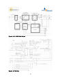
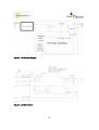
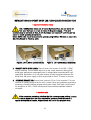
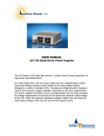
USER MANUAL
preliminary
LDD / LDY – LDDHC / LDYHC - CW Laser Diode Drivers
LDD- / LDY-series
LDDHC- / LDYHC-series
1
2
Overview:
The LDD / LDDHC family represents the Lumina Power standard DC power supply for
driving high power CW laser diodes.
Due to most principle features and control of LDD/LDY resp. LDDHC/LDYHC
being identical, in this manual LDD/LDDHC is meant representative also for
analogous models of LDY/LDYHC.
For differences between LDD / LDY and LDDHC / LDYHC refer to page 5 and Table 1 a)
and b) at page 11/12 (interface schematics).
As laser diode driver, the LDD / LDDHC power supply acts as a programmable current
source and delivers constant current based on the input program signal, which is
normally 0 – 10 V.
All units are configured with a maximum current and maximum voltage capability,
depending on the user requirements. Nomenclature is LDD / LDDHC-zz-xx-yy where zz
represents the max. power delivered by the specific unit, xx max. current and yy the max.
voltage configuration (refer page 9/10). LDD / LDDHC power supplies will deliver current
as programmed into any load, provided that the voltage requirements of that load do not
exceed the maximum rated voltage of the unit.
SAFETY WARNING
Depending on the output configuration of the LDD the output voltage might
exceed 48 VDC. Higher voltages than 48 VDC must be considered extremely
dangerous, and as such, care must be taken to not touch the output terminals
SAFETY WARNING
Because LDD / LDDHC units are designed for OEM applications, the user must
connect AC input power to the power supply.
Any input AC voltage must be considered extremely dangerous, and as such, care must
be taken to connect AC input power to the unit.
3
Important notes:
With the new revision of the LDD/LDY (from 06/2008 on) besides LDY modells also the
LDD-600 – LDD-1500 family includes the following additional features:
•
•
Current Limit Dip Switches: A bank of 4 DIP switches is provided to limit the
output current to 16 settings between 110% and 56% of maximum output. This
is a useful feature in the event that the diode driver is to be used for multiple
applications with some applications requiring less than the maximum rated
current of the LDD.
Protection circuit against current overshoots: The unit will be disabled
immediately in case of an AC power failure to protect the laser diode against
current overshoots. Also in case of a load disconnection (e.g. cable break or loose
contact) the unit will shut down.
-> For automatic restart after an AC failure, option – RE might be choosen
although this is not recommended as current overshoots might not be aviodable.
Use of –RE is at users own risk.
Common features:
•
•
Current Modulation: Although the LDD / LDDHC is designed as CW driver
nevertheless it is possible to change the current value fast. If current modulation
faster than 20 Hz sinusoidal is planned, the LDD / LDDHC with fast rise option -FR
is recommended. LDD fast rise-models are appropriate
for sinusoidal current modulation up to 500 Hz. For
exemplary values of option -FR refer to Appendix 2.
For more information on LDDHC with option -FR please
contact Schulz-Electronic.
Optional features: If any special configuration or
accessory is needed, please contact Schulz-Electronic.
Optional accessory: LDD-Contoller
- A remote control box LDD-controller is available
optionally for current control via 10-turn poti and current and voltage monitoring
by display.
- For simmering laser diodes below the threshold
current of the connected laser diode an adjustable idle
current modul can be provided. For details contact
Schulz-Electronic.
The LDD / LDDHC is a competitive laser diode driver with all
basic features for operating high power laser diodes. For even
higher functionality LDY / LDYHC series is provided.
4
Optional accessory: Idle current
module
Features / differences of LDY / LDYHC:
The LDY / LDYHC-family is the recommended laser diode driver series, if additional safety
features and pulsing capability via TTL-signal are required:
1. LDY/LDYHC contains a crowbar at the output, that is shortend in case of
- disabled status
- overvoltage detection
to protect the connected load.
2. Over voltage protection: LDY / LDYHC detects if the load voltage exceeds the rated
voltage. E.g. a LDY-1000-80-12 will shut of if the load voltage requirement exceeds about
12 V. Also in case of a load disconnection (e.g. cable break or loose contact) the unit will
shut down.
3. Protection circuit against current overshoots: The unit will be disabled immediately in
case of an AC power failure to protect the laser diode against current overshoots.
If the control signals to the D-sub interface remained during AC off, at AC recovery the
unit will NOT switch by itself.
-> Pin 1 has to be disabled and re-enabled to start up the unit again.
4. Current Limit Dip Switches: A bank of 4 DIP switches is provided to limit the output
current to 16 settings between 110% and 56% of maximum output (refer to page 19).
This is a useful feature in the event that the diode driver is to be used for multiple
applications with some applications requiring less than the maximum rated current of the
LDD.
5. Pulse control allows fast output on/off by applying a TTL signal to Pin 8 of the control
interface (see page 11/12).
6. Over temperature warning: Delivers +5 V output, if internal heat sink temperature
exceeds 65 °C. This signal might be used e.g. for switching external fans etc.
LDD*1) / LDDHC power supplies utilize a proprietary low loss, high frequency power factor
correction circuit which keeps power factor above 0.98. Power factor corrected power
supplies use up to 30% less input current and meet stringent IEC harmonic
requirements. The output inverter is a state-of-the-art zero voltage switching (ZVS)
inverter which permits very high frequency power conversion with minimum losses and
electromagnetic noise.
*1)
LDD-50 is a series pass type power supply (see figure 5). The AC/DC supplies output
voltage must be adjusted to the expected load condition for keeping losses low.
ð Load voltage must be near max. rated output voltage (e.g. do NOT use a 1 V load with a 3
V rated unit).
5
LDD / LDDHC Diode Drivers - Theory of Operation
(Refer to figure 1)
The LDD / LDDHC laser diode drivers were designed specifically for the OEM high power
CW laser diode systems. OEM power supplies for the laser diode industry have the
following requirements:
•
•
•
•
•
•
•
Safe laser diode operation
Broad range of control of output current
Safe rise/fall times
Small size
Power factor correction to conform with CE requirements
Low conducted electromagnetic emissions
Low leakage for medical applications
Referring to the “LDD / LDDHC Laser Diode Power Supply” block diagram (figure 1), the
following is a brief description of operation.
AC Input Power Circuitry
AC input power is processed through a line filter to reduce the conducted EMI to an
acceptable level. The LDD / LDDHC line filter has minimum capacitance to ground to
minimize leakage currents. Earth Ground stud is provided near the AC input terminals and
should be connected to the system ground.
To limit the inrush current, the equipment features a NTC resistor in the input circuit. On
reaching the operating temperature, the resistor has a low impedance and this means
even higher inrush current when switching on the equipment again immediatly after
switching it off.
The size of the maximum inrush current is limited by the internal resistance of the
equipment, the lead resistance and the impedance of the main.
So that the inrush current for a cold unit is not exceeded, the power supply has to
remain switched off at an ambient temperature of ≤ 25°C for approx. 5 minutes.
Depending on the power configuration the inrush current can reach from 20 A up to 50 A
at cold start-up.
Example for inrush current pulse shape see Appendix 1
Power Factor Correction Boost Inverter
The rectified input power is next applied to power factor boost inverter. This inverter
boosts the input voltage to 400 VDC. In the process of boosting the input AC voltage, the
input AC current is adjusted so that is always in phase with the input AC voltage.
Without this power factor correction circuit, the AC input current would be delivered to
the power supply in high amplitude, narrow spikes, having a high harmonic content. With
power factor correction, the non-50/60 Hz harmonics are reduced to near zero. Since only
6
the fundamental frequency is now used to deliver power, the efficiency of the power
supply is improved considerably.
One problem with standard input power factor correction circuits is that a high frequency
switching circuit is placed across the line in the input side of the traditional input
capacitor filter. This results in substantial switching noise conducted to the line. Lumina
Power employs a proprietary soft-switching boost inverter which produces minimum
switching noise, reduces switching losses, and results in a smaller heat sink associated
with the power factor circuit.
7
Zero Voltage Switching (ZVS) Inverter
The ZVS inverter and the output transformer are used to step the 400 VDC bus down to
the appropriate output value. The ZVS inverter is the most modern high frequency/low
loss/low noise topology utilized in power electronics today. Instead of running the
inverter in a traditional PWM mode, the inverter is run in a phase shift mode. With the
appropriate output inductor and the appropriate capacitance across each switching
device, in this case MOSFETS, there are virtually no switching losses in the inverter. The
only losses in the devices are I2R losses associated with the Drain/Source resistance of
the MOSFETS. Therefore, the ZVS inverter also contributes to reduced losses, reduce EMI
noise and a reduction in overall system heatsink requirements.
Output Circuit
The output filter is a two stage RC filter designed to keep ripple and output noise very
low. For lower power units, such as the LDD-250, a single stage filter is used.
Control Circuit
The control circuit handles all the responsibilities associated with safe operation of the
laser diode. Controlled rise and fall times, as well as tight current regulation, overvoltage
and over power protection are controlled and monitored in the control circuit.
Auxiliary Power
All internal power supply requirements as well as the external +/-15 V and +5 V power
supplies are derived from the power factor control boost inductor. All auxiliary power
supplies are regulated by standard linear regulators.
Note: LDD-50 does not incorporate auxiliary outputs.
8
LDD-50- to LDD-3000-xx-yy Specifications
xx = Iout, max / yy = Vout, max / xx * yy cannot exceed Pout, max
Model
LDD-50-xx-yy
*1)
Pout, max
Iout, max
Input Voltage *2)
Size (L x W x H)
50 W
Up to 15 A
90 – 264 VAC
171 x 92 x 83 mm
LDD-100-xx-yy
100 W
5 A to 50 A
LDD-150-xx-yy
150 W
10 A to 60 A
LDD-250-xx-yy
250 W
LDD-400-xx-yy *2)
400 W
LDD-600-xx-yy
600 W
LDD-1000-xx-yy
1.000 W
LDD-1500-xx-yy
*2)
1.500 W
LDD-3000-xx-yy
*2)
4.000 W
Auxiliary Outputs :
*1)
*1)
*2)
10 A to 80 A
10 A to 100 A
90 – 264 VAC
90 – 264 VAC
190 x 147 x 66 mm
180 – 264 VAC
90 - 264 VAC
251 x 185 x 66 cm
180 – 264 VAC
Up to 200 A
180 – 264 VAC
432 x 422 x 86 mm
+5 V @ 0.5 A
+15 V @ 0.5 A
-15 V @ 0.5 A
No auxiliary voltages available at LDD-50
LDD-400, LDD-1500 and LDD-3000 input voltage: 180 - 264 VAC
Maximum compliance voltage determined by maximum rated power
RS-232 option available
Other outputs available upon request
Input
Voltage:
Power Factor:
See table above
> 0.98
Interface
Connector:
Current Program:
Current Monitor:
Voltage Monitor:
15 Pin “D” Sub Female
0 – 10 V for 0 – Max. current
0 – 10 V for 0 – Max. current
0 – 10 V for 0 – Max. voltage
Performance
Pulse Width Range:
Rise/Fall Time:
Current Regulation::
Current Ripple:
Current Overshoot:
Power Limit:
<2 ms to CW
<1 ms (10% to 90% full current), <500 µs with option – FR
0.5% of maximum output current
<0.5% of maximum output current
<1% of maximum output current
Limited to maximum power with power fold-back circuit
Environment
Operating Temp:
Storage:
Humidity:
Cooling:
0 to 40 °C
-20 to 85 °C
0 to 90% non-condensing
Forced air
Regulatory
Leakage Current:
<250 µA
Approvals
Industrial Safety
Medical Safety:
M90
Emissions/Immunity:
LDD-150/250/400/600/1.000/1.500 UL60950
LDD-600/1.000/1.500: UL60601-1, IEC 60601-1, EN 60601-1, CAN/CSA C22.2 No. 601.1FCC 47 CFR Class A Emissions, EN55011:1998 Group 1 Class A Emissions, EN61000-3-2
Limits for harmonic current emissions, EN 610000303 Flicker, EN60601-1-2:2001
Electromagnetic emissions and immunity for medical equipment
9
LDDHC-600- to LDDHC-1.500-xx-yy Specifications
xx = Iout, max / yy = Vout, max / xx * yy cannot exceed Pout, max
Model
Poutmax
LDDHC/LDYHC-600-xx-yy
600 W
LDDHC/LDYHC-1000-xx-yy
1.000 W
LDDHC/LDYHC-1500-xx-yy*
1.500 W
Auxiliary Outputs:
Ioutmax
Input Voltage
Size (L x W x H)
90 - 264 VAC
110 A to 200 A
260 x 203 x 70 cm
180 – 264 VAC
+5 V @ 0.5 A
+15 V @ 0.5 A
-15 V @ 0.5 A
* LDDHC/LDYHC-1500 input voltage: 180 - 264 VAC
Maximum compliance voltage determined by maximum rated power
RS-232 Option available
Other outputs available upon request
Input
Voltage:
Power Factor:
See table above
> 0.98
Interface
Connector:
Current Program:
Current Monitor:
Voltage Monitor:
15 Pin “D” Sub Female
0 – 10 V for 0 – Max. current
0 – 10 V for 0 – Max. current
0 – 10 V for 0 – Max. voltage
Performance
Pulse Width Range:
Rise/Fall Time:
Current Regulation::
Current Ripple:
Current Overshoot:
Power Limit:
<2 ms to CW
<1 ms (10% to 90% full current), <700 µs with option – FR
0.5% of maximum output current
<0.5% of maximum output current
<1% of maximum output current
Limited to maximum power with power fold-back circuit
Environment
Operating Temp:
Storage:
Humidity:
Cooling:
0 to 40 °C
-20 to 85 °C
0 to 90% non-condensing
Forced air
Regulatory
Industrial Safety
Emissions/Immunity:
Designed to comply with UL60950, UL60601.1
Designed to comply with FCC 47 CFR Class A Emissions, EN55011:1998
Group 1 Class A Emissions, EN61000-3-2, EN 610000303, EN60601-1-2:2001
10
The LDD-Family is available from 50 to 4.000 W. The auxiliary power and available
approvals depend on the model power and configuration. Please have a look on the
actual data sheet overview.
LDD-50 – 4.000 / LDDHC-600 – 1500 Interface
Connector Type: 15 pin D-sub Female
Pin #
LDD Pin Name
Functional Voltage Level
1
Enable
(input)
2
NC
(output)
3
Interlock
(input)
Open = OFF
Connect to GND = RUN
The Interlock function must be connected to GND in order for output current
to be delivered. It can be used for external interlock functions such as door
or overtemp. switches.
5
V out, Monitor
(output)
0 – 10 V = 0 – Vout, max
The output voltage of the supply can be monitored by Vout, Monitor. For LDD’s
with a maximum rated output voltage less than 10 V, Vout, Monitor = Vout. For
output voltages greater than or equal to 10 V, 0 – 10 V = 0 – Vout, max..
6
Iout, Monitor
(output)
0 – 10 V = 0 – Iout, max
The output current of the supply can be monitored by Iout, Monitor .
7
Iprogram(+)
(input)
0 – 10 V = 0 – Iout, max
The power supply output current is set by applying a 0 – 10 V analog signal
to Iprogram(+).
8
NC / (Pulse control
for LDD-3000 only)
(input)
10
+5 V @ 0.25 A *
(output)
11
+5 V @ 0.25 A *
(output)
12
-15 V @ 0.5 A *
(output)
Auxiliary -15 V power supply for user. Up to – 0.5 A output current available.
(max. current outout for LDD-100 – 250 = 100 mA)
13, 14
+15 V @ 0.5 A *
(output)
Auxiliary +15 V power supply for user. Up to +0.5 A output current available.
(max. current outout for LDD-100 – 250 = 100 mA)
4, 9, 15
GND
Interface return
High = RUN = +5 V to +15 V
Low = OFF = 0 V
Description
The Enable function turns the output section of the power supply ON and OFF.
When the power supply is enabled, current is delivered to load as
programmed via Iprogram(+), Pin 7 if the Interlock, Pin 3 is connected to interface
GND. Rise times resulting from Enable are approximately 25 ms.
Please do not connect this pin
TTL High = On
TTL Low = Off
The output of the LDD-3000 may be pulsed by applying a TTL signal to Pulse
Control, pin 8. The amplitude of the output current pulse is determined
by the current level programmed via Pin 7, Iprogram(+). Rise fall times of <1msec
are typical. If left unconnected, the default will be ON for CW operation.
Auxiliary +5 V power supply for user. Up to 0.5 A output current capability on
Pin 10 and 11 together. (max. current outout for LDD-100 – 250 = 100 mA)
* no auxiliary power output for LDD-50
Table 1 a: LDD / LDDHC Interface
For more detailed interface information please refer to figure 2
11
LDY-600 – 1500 / LDYHC-600 – 1500 Interface
Connector Type: 15 pin D-sub Female
Pin #
LDD Pin Name
1
Enable
(input)
Functional Voltage Level
Description
High = RUN = +5 V to +15 V
Low = OFF = 0 V
The Enable function turns the output section of the power supply ON and OFF.
When the power supply is enabled, current is delivered to load as
programmed via Iprogram(+), Pin 7 if the Interlock, Pin 3 is connected to interface
GND. Rise times resulting from Enable are approximately 25 ms.
High = Crowbar OFF = +5 V
Low = Crowbar ON = 0 V
The Crowbar Status reports the status of the shorting crowbar clamp across
the output. The crowbar will short the output under two conditions:
1) When the output is not ENABLED via Pin 1, or, 2) if the output is ENABLED
via pin 1 but the control circuitry has detected a no- load condition or a
voltage requirement on the output that exceeds the maximum voltage rating
of the unit. A TTL+5V signal on Pin 2 reports that the crowbar is shorting the
output. To turn the crowbar off, an appropriate load must be connected to the
LDD and the output must be turned off and on via Pin 1, ENABLE.
2
Crowbar status
(output)
3
Interlock
(input)
Open = OFF
Connect to GND = RUN
The Interlock function must be connected to GND in order for output current
to be delivered. It can be used for external interlock functions such as door
or overtemp. switches.
5
V out, Monitor
(output)
0 – 10 V = 0 – Vout, max
The output voltage of the supply can be monitored by Vout, Monitor. For LDD’s
with a maximum rated output voltage less than 10 V, Vout, Monitor = Vout. For
output voltages greater than or equal to 10 V, 0 – 10 V = 0 – Vout, max..
6
Iout, Monitor
(output)
0 – 10 V = 0 – Iout, max
The output current of the supply can be monitored by Iout, Monitor.
7
Iprogram(+)
(input)
0 – 10 V = 0 – Iout, max
The power supply output current is set by applying a 0 – 10 V analog signal
to Iprogram(+).
TTL High = On
TTL Low = Off
The output may be pulsed by applying a TTL signal to Pulse Control, pin 8.
The amplitude of the output current pulse is determined by the voltage
programmed via Pin 7, Iprogram(+). Rise fall times of <1 ms are typical.
Rise fall times of <500 µs can be achieved with special order. When using the
LDY / LDYHC as a CW diode driver, pin 8, the Pulse Control, must be set to
TTL High in order for output current to be delivered. Pin 10, +5V, would be a
convenient connection point for this. No output current will be delivered with
pin 8 left unconnected.
8
Pulse control
(input)
10
+5 V @ 0.5 A *
(output)
11
Over-Temp warning
(output)
12
-15 V @ 0.5 A *
(output)
Auxiliary -15 V power supply for user. Up to – 0.5 A output current available.
13, 14
+15 V @ 0.5 A *
(output)
Auxiliary +15 V power supply for user. Up to +0.5 A output current available.
4, 9, 15
GND
Interface return
Auxiliary +5 V power supply for user. Up to 0.5 A output current capability on
Pin 10 and 11 together.
TTL High = High Temp
TTL Low = Temp OK
When temperature of main heat sink exceeds 65 Deg C, Pin 11, the OverTemp Warning, will go to a TTL High to indicate unit is in danger of shutting
down due to over-temperature condition. When temperature of
main heat sink exceeds 75 Deg C, unit will shut down.
Table 1 b: LDY / LDYHC Interface
12
Figure 1: LDD / LDDHC block diagram
Figure 2: LDY interface
13
Figure 3: LDD-50 block diagram
Figure 4: LDD-50 interface
14
INSTALLATION AND OPERATION OF LDD / LDDHC LASER DIODE DRIVERS
Important installation notes
LDD / LDDHC diode drivers are air cooled by internal fans. Do not restrict air
flow near the input or output air vents of the power supply. If the unit
overheats due to restricted air flow, it will shut down and remain off until the unit has
cooled to a safe operating temperature.
LDD / LDDHC units should be mounted in systems using 8-32 (or M4) bolts to secure the
mounting flanges to mounting plate.
Figure 5: LDD / LDDHC Input Connections
Figure 6: LDD / LDDHC Output Connections
1. CONNECTING TO DIODE LASER: Figure 6 shows the location of the LDD / LDDHC
output terminals. Connect diode laser load to the output terminals. Although CW
diode laser applications are generally free of voltage spikes associated with high
speed QCW applications, it is still good practice to keep connections between the
diode laser and power supply as short as possible to avoid I2R losses in the wire.
2. INTERFACE CONNECTION: Connect user system to 15 pin D-sub connector. The user
interface is typically designed by the user, Lumina Power can provide any assistance
necessary to modify interface program and monitor levels. See Table 1 and Figure 2
for description of LDD / LDDHC interface and the associated simplified interface
schematic.
Important note
Make sure when connecting interface that the current program setting, Iprogram(+),
is set no higher then the value required for operation. When AC power is
applied and system is Enabled, output current will rise to this program value.
15
3. AC INPUT POWER CONNECTION
SAFETY WARNING
Because LDD / LDDHC units are designed for OEM applications, the user must
connect AC input power to the power supply.
Any input AC voltage must be considered extremely dangerous, and as such, care must
be taken to connect AC input power to the unit.
Important note
- AC input wires should be at least #16 AWG, rated for at least 300 V at 105 °C
- LDD / LDDHC units are fused on both input lines. It does not matter which of
the two AC inputs are designated Line or Neutral
Connect AC power connections to power supply input power terminals as follows:
• Neutral wire (16 AWG) connected to the right contact of the AC input terminal.
• Line wire (16 AWG) connected to the left contact of the AC terminal block.
• Ground wire shall be crimped to a #8 ring-lug and connected to the ground stud.
LDD Model:
CE Med 60601-1
UL 60950
LDD-50
LDD-100
ü
ü
ü
ü
LDD-150
ü
LDD-250
ü
LDD-400
ü
ü
LDD/LDY-600
ü
ü
LDD/LDY-1000
ü
ü
LDD/LDY-1500
LDD-3000
ü
ü
ü
LDDHC/LDYHC-600
ü
ü
LDDHC/LDYHC-1000
*1)
ü contact Schulz-Electronic
ü
LDDHC/LDYHC-1500
For further information please
Input
90 - 264 VAC
90 - 264 VAC
ü
ü
ü
ü
ü
ü
ü
ü
ü
90 - 264 VAC
90 - 264 VAC
180 - 264 VAC
90 - 264 VAC
90 - 264 VAC
180 - 264 VAC
180 - 264 VAC
90 - 264 VAC
90 - 264 VAC
180 - 264 VAC
Table 2: LDD/LDY – LDDHC/LDYHC approval overview and input voltage
16
MODEL
LDD-100
LDD-150
LDD-250
LDD-400
LDD/LDY-600
LDD/LDY-1000
LDD/LDY-1500
LDDHC/LDYHC-600
LDDHC/LDYHC-1000
LDDHC/LDYHC-1500
INPUT POWER
Input: 100 –
Input: 100 –
Input: 100 –
Input: 200 –
Input: 100 –
Input: 100 –
Input: 200 –
Input: 100 –
Input: 100 –
Input: 200 –
240 VAC, 50/60
240 VAC, 50/60
240 VAC, 50/60
240 VAC, 50/60
240 VAC, 50/60
240 VAC, 50/60
240 VAC, 50/60
240 VAC, 50/60
240 VAC, 50/60
240 VAC, 50/60
Hz, 2.4 A – 1 A.
Hz, 3.6 A – 1.5 A
Hz, 6.5 A – 3 A
Hz, 6 A – 4.5 A
Hz, 11.5 A – 5.5 A
Hz, 15 A – 6.5 A
Hz, 9.5 A – 7.5 A
Hz, 13.5 A – 6.5 A
Hz, 17 A – 7.5 A
Hz, 11 A – 8.5 A
June 10
Table 3: LDD/LDY, LDDHC/LDYHC AC input power requirements
4. OPERATING THE DRIVER
Switch on procedure:
The unit may be programmed for output current via Pin 7, the Iprogram function. But
there are two interface control signals which must be properly set before the output
will deliver current as programmed by Iprogram.
a. AC-power must be connected
b. INTERLOCK: Pin 3, the Interlock, must be grounded via Pins 4, 9 or 15 to let the
output section be activated by the ENABLE Pin 1.
c. ENABLE: Pin 1, the ENABLE signal is a +5 V to +24 V signal used to turn the output
section on. The ENABLE circuitry incorporates a soft start function which ensures rise
times of approximately 15 to 20 ms.
d. Iprogram: Pin 7, an analog 0 – 10 V signal results in 0 to Iout, max, as long as the rated
compliance voltage of the driver is not exceeded
CH 1
Iout
20A/div
CH 2
ENABLE
Figure 7: Response of Iout to ENABLE signal
17
CH 1
Iout
20 A / div
CH 2
Pin 8: TTL
Figure 8: Typical LDD /LDY rise fall time
It is possible to configure LDD / LDY’s for rise and fall times up to 500 µs, which would
permit pulsing up to 600 Hz (Figure 8). Consult Schulz-Electronic for faster rise/fall times.
Typical rise/fall times for LDDHC / LDYHC are up to 1 ms.
Pulsed output is delivered when fast switching the current programming signal (pin 7,
Iprogramm(+)) between low/high (LDD and LDY) or switching pin 8 between TTL low/high
(LDY only).
NOTE: It is not possible to use Enable, Pin 1, for pulsing since the ENABLE circuit
includes a “soft start” is intended for turning on the power supply output slowly (see
figure 7). The Enable function controls several soft-start features which do not permit
pulsing.
NOTE: For faster pulsing, refer to the data sheet for Lumina Power’s LDQCW power
supplies. These units have rise/fall times of less than 25 µs and can achieve output
currents up to 200 A. These units can pulse at frequencies up to 5 kHz, depending on
the average power required.
ð For further information contact Schulz-Electronic.
18
Important note
If the unit is first enabled and AC power is switched on afterwards, the unit
will not deliver current. The unit will need to be reset first: The unit must
be disabled and enabled again.
LDD-100 – LDD-1500 and LDY/LDYHC: In case of voltage overshoots due to e.g. a
loose contact at the output or in case of a short AC drop out the unit will
immediately shut down and will also need to be reset again.
For automatic start up after a safety shut down option – RE is available.
5. MONITORING LDD / LDDHC OUTPUT AND PERFORMANCE:
a. Current Monitor: Power supply output current can be monitored via pin 6, Iout, monitor : A
0 – 10 V signal will represent the output current from 0 to maximum rated output
current.
b. Voltage Monitor: Power supply output voltage can be monitored via pin 5, Vout, monitor :
A 0 – 10 V signal will represent the output voltage from 0 to maximum rated output
voltage.
6. Programmable Current Limit DIP Switches The LDD-/LDY-600 – LDD-/LDY-1500
includes an internal DIP switch array which may be set to limit the maximum
current. This is useful when an OEM customer would like to use a single model for a
variety of systems, but has a laser diode system which does not require the
maximum output current. In this type of situation, it is important to protect the laser
diode from an over-program error which could damage the laser diode. The following
table shows the various DIP switch settings and resulting output current.
S1
S2
S3
S4
Imax, out
OFF
OFF
OFF
OFF
110%
OFF
OFF
OFF
ON
103%
OFF
OFF
ON
OFF
98%
OFF
OFF
ON
ON
92%
OFF
ON
OFF
OFF
88%
OFF
ON
OFF
ON
84%
OFF
ON
ON
OFF
80%
OFF
ON
ON
ON
77%
ON
OFF
OFF
OFF
74%
ON
OFF
OFF
ON
70%
ON
OFF
ON
OFF
68%
ON
OFF
ON
ON
65%
ON
ON
OFF
OFF
63%
ON
ON
OFF
ON
60%
19
ON
ON
ON
OFF
58%
ON
ON
ON
ON
56%
For example, if an LDD is configured for a maximum output current rating of 60 A,
and the maximum output current should be limited in a particular application to 40 A,
the DIP switch array should be set as follows:
S1
S2
S3
S4
Imax, out
ON
OFF
ON
OFF
68%
This will limit the current to 68% of 60 A, means approx. 40 A. When the unit is
programmed with a 0 - 10 V signal, the output will follow the programming voltage
until the analog signal reaches 6.8 V. Programming to more than 6.8 V, means 68%
of 10 V, the output current will not rise any further.
Units are shipped with all switches in the OFF position (upwards position), which
results in the ability to program the unit with up to 110% programming voltage.
Nevertheless the output current will never exceed 100% of the maximum rated
current.
Important application note
When the power supply is enabled using the ENABLE signal, internal soft
start function limits the rise time of the output current to approximately
20 ms. Once the power supply is enabled, the rise/fall time caused by Iprogram(+) signal
is approximately 600 µs (LDD / LDY) / 1 ms (LDDHC / LDYHC).
Important application note
When the internal heat sink temperature reaches 75 °C, the unit will shut
down.
Servicing Lumina Power laser diode drivers
All modells LDD / LDY / LDDHC / LDYHC have no serviceable parts. Do not attempt to
repair or service this unit in the field. For further information, contact Schulz-Electronic:
[email protected]
+49 (0)7223 9636-48
20
Appendix 1
Example of LDD inrush current
LDD-600-85-3 (Input section the same for LDD/LDY-600/1000/1500)
Input = 115 VAC / 60 Hz
Ch: 2 = 10 A / division
Ipeak < 50 A
Appendix 2
Option – FR / current modulation
The fast rise option allows steep rise and fall times of under 500 µs.
Additionally fast modulation is possible.
E.g. a unit LDY-1500-80-19-FR was tested to approximately following limits:
- Sinusoidal modulation up to 500 Hz between 20 and 100% current amplitude
- Stepwise modulation of the output current between 70 and 90% load. The unit
follows with a slew rate of ca. 16 A/100 µs and a regulation delay of 50 µs. Here
current modulation is possible up to a sampling rate of 4 kHz at programming
steps of ±20% every 250 µs.
21
Appendix 3
Guidelines
EN55011 Class A
Lumina products comply with EN55011:1988 Group 1 Class A Emissions.
These products are designed for industrial application and hence comply with this
guideline in respect of emission and immission in industrial environment. They may not
comply with domestic standard (class B) regarding emission.
RoHS
EU Guideline 2002/95/EG
The reduction of the pollutants in the products of the electrical industry is an important
contribution to the environment protection which earns the biggest support from us all.
This rearrangement process was concluded at Lumina Power Inc. in year 2007. All
Lumina Power laser diode drivers, which are produced after 2007 are RoHS-compliant.
22