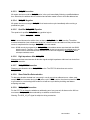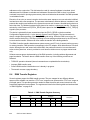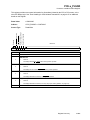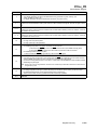
1
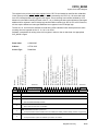
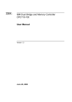
CPC710 PCI Bridge
and Memory Controller
User Manual
SA14-2571-02
Fourth Edition (September 2002)
This edition of the IBM CPC710 PCI Bridge and Memory Controller User Manual applies to the IBM CPC710
PCI bridge and memory controller, until otherwise indicated in new versions or application notes.
© Copyright International Business Machines Corporation 2002
All Rights Reserved
Printed in the United States of America September 2002
The following are trademarks of International Business Machines Corporation in the United States, or other countries,
or both.
IBM
IBM Logo
CoreConnect
PowerPC
PowerPC logo
PowerPC Architecture
RISCTrace RISCWatch
Other company, product, and service names may be trademarks or service marks of others.
All information contained in this document is subject to change without notice. The products described in this document are NOT intended for use in implantation, life support, space, nuclear, or military applications where malfunction
may result in injury or death to persons. The information contained in this document does not affect or change IBM
product specifications or warranties. Nothing in this document shall operate as an express or implied license or indemnity under the intellectual property rights of IBM or third parties. All information contained in this document was
obtained in specific environments, and is presented as an illustration. The results obtained in other operating environments may vary.
THE INFORMATION CONTAINED IN THIS DOCUMENT IS PROVIDED ON AN “AS IS” BASIS. In no event will IBM
be liable for damages arising directly or indirectly from any use of the information contained in this document.
IBM Microelectronics Division
1580 Route 52, Bldg. 504
Hopewell Junction, NY 12533-6351
The IBM home page can be found at http://www.ibm.com
The IBM Microelectronics Division home page can be found at http://www.ibm.com/chips
ii
CPC710 User’s Manual
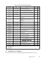
Contents
About This Book ..................................................................................................................... xiii
Chapter 1. Overview ...............................................................................................................1-1
Features ...........................................................................................................................................................
60x Bus Interface ........................................................................................................................................
Memory Controller .......................................................................................................................................
PCI-32 and PCI64 Bus Bridges ...................................................................................................................
1-1
1-1
1-2
1-2
Chapter 2. Addressing Model ...............................................................................................2-1
Address Maps ..................................................................................................................................................
CPU to PCI Addressing Model .........................................................................................................................
PREP and FPHB Modes .............................................................................................................................
CHRP Mode ................................................................................................................................................
Peripheral I/O Address Translation .............................................................................................................
PCI to System Memory ....................................................................................................................................
PowerPC Reference Platform (PREP) Mode ..............................................................................................
PCI Master Address Operation ...............................................................................................................
Translation Enabled in PREP Mode .......................................................................................................
Translation Disabled in PREP Mode .......................................................................................................
Flexible PCI Host Bridge (FPHB) Mode ......................................................................................................
CHRP Address Map ....................................................................................................................................
2-1
2-2
2-2
2-3
2-4
2-5
2-6
2-6
2-6
2-7
2-8
2-9
Chapter 3. System I/O Interface ............................................................................................3-1
Configuration ....................................................................................................................................................
System I/O Registers: Application Presence Detect Bits .................................................................................
Flash Interface .................................................................................................................................................
Boot Rom ....................................................................................................................................................
Extended Boot Flash ...................................................................................................................................
Byte ordering in the Boot & Extended Flash for 8 bit bus size: ...................................................................
3-1
3-1
3-1
3-1
3-2
3-2
Chapter 4. 60x Interface .........................................................................................................4-1
Endian Support ................................................................................................................................................
PowerPC Processor Behavior Mode ...........................................................................................................
Processor Behavior in LE Mode .............................................................................................................
Endian Behavior .....................................................................................................................................
60x Bus Arbiter Description .............................................................................................................................
Rotating Priority Resolution .........................................................................................................................
Address Bus Pipelining ...............................................................................................................................
Arbiter Requirements ..................................................................................................................................
Internal ABB ............................................................................................................................................
Qualified SYS_BG Equation ...................................................................................................................
SYS_TS Assertion ..................................................................................................................................
SYS_BR Negation ..................................................................................................................................
Qualified SYS_DBG Equation ................................................................................................................
High Impedance After SYS_TEA ............................................................................................................
SYS_DRTRY Assertion ..........................................................................................................................
Slave Data Bus Determination ................................................................................................................
SYS_L2_Hit Assertion ............................................................................................................................
Bus Enhancements .....................................................................................................................................
DBB not Required by Masters ................................................................................................................
Half-Cycle Precharge not Required on SYS_TA ....................................................................................
SYS_ARTRY_PREV in QDBG Equation Eliminated ..............................................................................
60x Bus Transfer Types and Sizes .............................................................................................................
Contents
4-1
4-4
4-4
4-4
4-5
4-6
4-6
4-6
4-6
4-6
4-7
4-7
4-7
4-7
4-7
4-7
4-7
4-8
4-8
4-8
4-8
4-8
iii
Data Gathering ..............................................................................................................................................
SYNC and EIEIO ...........................................................................................................................................
Address Retry (SYS_ARTRY) .......................................................................................................................
Precharging SYS_ARTRY and SYS_SHD ...............................................................................................
SYS_ARTRY Assertions ...........................................................................................................................
Recommended SYS_ARTRY Procedure ..................................................................................................
Deadlock Avoidance ......................................................................................................................................
Deadlock Avoidance Operation with Internal Logic ..................................................................................
Deadlock Avoidance Operation with External Logic .................................................................................
Error Handling for CPU-Initiated Transactions ..............................................................................................
Checkstop Errors ......................................................................................................................................
4-10
4-11
4-12
4-12
4-12
4-12
4-13
4-14
4-15
4-15
4-15
Chapter 5. Initialization .......................................................................................................... 5-1
CPC710 Power Up Sequence: ........................................................................................................................
POWERGOOD Power-On Reset ....................................................................................................................
PLL for Clock System ......................................................................................................................................
Initialization of the SDRAM ..............................................................................................................................
Reset Individual Devices .................................................................................................................................
Reset in Multiprocessor mode .........................................................................................................................
Typical Register Setup Sequence ...................................................................................................................
5-1
5-1
5-2
5-3
5-4
5-4
5-5
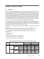
Chapter 6. Memory Controller ............................................................................................... 6-1
Overview .......................................................................................................................................................... 6-1
Bank Definitions ............................................................................................................................................... 6-2
SDRAM Banks ............................................................................................................................................ 6-2
DIMM Banks ............................................................................................................................................... 6-2
Interleaved Banks ....................................................................................................................................... 6-2
Memory Signal Connections ............................................................................................................................ 6-3
SDRAM Subsystem Overview ......................................................................................................................... 6-6
Supported SDRAM Organizations ................................................................................................................... 6-7
SDRAM Buffering Requirements ..................................................................................................................... 6-8
Typical SDRAM Signals .................................................................................................................................. 6-8
CKE (Clock Enable) Signal ......................................................................................................................... 6-9
Mapping of System address to SDRAM Memory address with the CPC710 .................................................. 6-9
Memory Controller Registers ......................................................................................................................... 6-11
SDRAM0_MCCR Register ........................................................................................................................ 6-11
SDRAM0_MCERx Registers .................................................................................................................... 6-14
Error Handling ............................................................................................................................................... 6-15
Single-Bit ECC Error, General Case ......................................................................................................... 6-16
Single-Bit ECC Error, Special Case .......................................................................................................... 6-16
Invalid Address Error ................................................................................................................................ 6-16
Double-Bit ECC Error, General Case ....................................................................................................... 6-16
Double-Bit ECC Error, Special Case ........................................................................................................ 6-17
Overlapping Memory Extents .................................................................................................................... 6-17
ECC Check-bit and Syndrome .................................................................................................................. 6-17
Single-Bit Error Correction ................................................................................................................... 6-18
Additionnal Information for Software .................................................................................................... 6-19
Chapter 7. PCI Bridges .......................................................................................................... 7-1
Address Map ...................................................................................................................................................
System Standard Configuration Registers ......................................................................................................
System PHB Registers ....................................................................................................................................
PCI Bus Commands ........................................................................................................................................
PCI Master Memory Read Cycles ...............................................................................................................
PCI Master Memory Write Cycles ...............................................................................................................
Configuration Cycles ...................................................................................................................................
Type 0 Configuration Cycles ..................................................................................................................
iv
CPC710 User’s Manual
7-1
7-1
7-2
7-2
7-2
7-3
7-4
7-6
Type 1 Configuration Cycles ................................................................................................................... 7-6
PCI Performance Estimates ............................................................................................................................. 7-6
PCI Master Error Handling ............................................................................................................................... 7-7
Chapter 8. DMA Controller ....................................................................................................8-1
Introduction ......................................................................................................................................................
Mode of operation of the DMA .........................................................................................................................
Starting the DMA ..............................................................................................................................................
DMA Transfer Registers ..................................................................................................................................
DMA Transfer Status Cache Line Descriptor for Chained DMA’s ...............................................................
DMA Procedure ...............................................................................................................................................
Special Boundary Conditions ......................................................................................................................
8-1
8-1
8-1
8-2
8-3
8-4
8-5
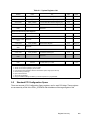
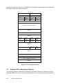
Chapter 9. Register Summary ...............................................................................................9-1
System Register Space ................................................................................................................................... 9-1
Standard PCI Configuration Space .................................................................................................................. 9-5
Standard PCI Configuration Registers ............................................................................................................. 9-6
Specific PCI Host Bridge Registers ................................................................................................................. 9-8
Alphabetical List of Registers ........................................................................................................................... 9-9
Chip Control Registers ............................................................................................................................... 9-10
CPC0_ABCNTL .................................................................................................................................... 9-10
CPC0_ATAS ......................................................................................................................................... 9-13
CPC0_AVDG ........................................................................................................................................ 9-15
CPC0_ERRC ........................................................................................................................................ 9-17
CPC0_GPDIR ....................................................................................................................................... 9-19
CPC0_GPIN ......................................................................................................................................... 9-20
CPC0_GPOUT ..................................................................................................................................... 9-21
CPC0_MPSR ........................................................................................................................................ 9-22
CPC0_PCIBAR ..................................................................................................................................... 9-23
CPC0_PCICNFR .................................................................................................................................. 9-24
CPC0_PCIENB ..................................................................................................................................... 9-25
CPC0_PGCHP ..................................................................................................................................... 9-26
CPC0_PIDR .......................................................................................................................................... 9-29
CPC0_RGBAN0 ................................................................................................................................... 9-30
CPC0_RGBAN1 ................................................................................................................................... 9-31
CPC0_RSTR ........................................................................................................................................ 9-32
CPC0_RTBR ........................................................................................................................................ 9-33
CPC0_SEAR ........................................................................................................................................ 9-34
CPC0_SESR ........................................................................................................................................ 9-35
CPC0_SIOC0 ....................................................................................................................................... 9-38
CPC0_SIOC1 ....................................................................................................................................... 9-40
CPC0_SPOR ........................................................................................................................................ 9-41
CPC0_SRST ......................................................................................................................................... 9-42
CPC0_UCTL ......................................................................................................................................... 9-43
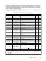
DMA Registers ........................................................................................................................................... 9-45
DMA0_GSCRP, DMA0_GSCRU
................................................................................................. 9-45
DMA0_XCLRP, DMA0_XCLRU ............................................................................................................ 9-47
DMA0_XPARP, DMA0_XPARU ........................................................................................................... 9-48
DMA0_XSCRP, DMA0_XSCRU ........................................................................................................... 9-49
DMA0_XSSRP, DMA0_XSSRU ........................................................................................................... 9-50
DMA0_XTARP, DMA0_XTARU ............................................................................................................ 9-52
DMA0_XWARP, DMA0_XWARU ......................................................................................................... 9-53
PCI Configuration Registers....................................................................................................................... 9-54
PCIC0_DLKRETRY .............................................................................................................................. 9-54
PCIC1_INTRESET ............................................................................................................................... 9-55
Contents
v
PCIC1_ITADDSET ............................................................................................................................... 9-56
PCIC1_PPBAR ..................................................................................................................................... 9-57
PCIC1_PSBAR ..................................................................................................................................... 9-58
PCICx_BIST ......................................................................................................................................... 9-59
PCICx_BUSNO .................................................................................................................................... 9-60
PCICx_CACHELS ................................................................................................................................ 9-61
PCICx_CLS .......................................................................................................................................... 9-62
PCICx_CMD ......................................................................................................................................... 9-63
PCICx_DEVID ...................................................................................................................................... 9-65
PCICx_DISCNT .................................................................................................................................... 9-66
PCICx_HDTYPE .................................................................................................................................. 9-67
PCICx_INTLN ....................................................................................................................................... 9-68
PCICx_INTPN ...................................................................................................................................... 9-69
PCICx_LATTIM .................................................................................................................................... 9-70
PCICx_MAXLTNCY ............................................................................................................................. 9-71
PCICx_MINGNT ................................................................................................................................... 9-72
PCICx_RETRY ..................................................................................................................................... 9-73
PCICx_REVID ...................................................................................................................................... 9-74
PCICx_STATUS ................................................................................................................................... 9-75
PCICx_SUBNO .................................................................................................................................... 9-77
PCICx_VENDID ................................................................................................................................... 9-78
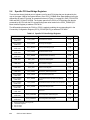
PCI Local Registers ................................................................................................................................... 9-79
PCIL0_PPBAR ..................................................................................................................................... 9-79
PCIL0_PSBAR ..................................................................................................................................... 9-80
PCIL1_INTSET ..................................................................................................................................... 9-81
PCIL1_ITADDRESET ........................................................................................................................... 9-82
PCILx_ACR .......................................................................................................................................... 9-83
PCILx_BARPP ..................................................................................................................................... 9-84
PCILx_BARPS ..................................................................................................................................... 9-85
PCILx_BIODLK .................................................................................................................................... 9-86
PCILx_BPMDLK ................................................................................................................................... 9-87
PCILx_CFGADDR ................................................................................................................................ 9-88
PCILx_CFGDATA ................................................................................................................................ 9-89
PCILx_CRR .......................................................................................................................................... 9-90
PCILx_CSR .......................................................................................................................................... 9-91
PCILx_CTRLW ..................................................................................................................................... 9-92
PCILx_DLKCTRL ................................................................................................................................. 9-93
PCILx_DLKDEV ................................................................................................................................... 9-95
PCILx_INTACK .................................................................................................................................... 9-96
PCILx_IOSIZE ...................................................................................................................................... 9-97
PCILx_MSIZE ....................................................................................................................................... 9-98
PCILx_PCIDG ...................................................................................................................................... 9-99
PCILx_PIBAR ..................................................................................................................................... 9-100
PCILx_PLSSR .................................................................................................................................... 9-101
PCILx_PMBAR ................................................................................................................................... 9-102
PCILx_PPSIZE ................................................................................................................................... 9-103
PCILx_PR ........................................................................................................................................... 9-104
PCILx_PSEA ...................................................................................................................................... 9-106
PCILx_PSRCR ................................................................................................................................... 9-107
PCILx_PSSIZE ................................................................................................................................... 9-109
PCILx_PSWCR .................................................................................................................................. 9-110
PCILx_SIBAR ..................................................................................................................................... 9-112
PCILx_SMBAR ................................................................................................................................... 9-113
PCILx_TIODLK ................................................................................................................................... 9-114
vi
CPC710 User’s Manual
PCILx_TPMDLK .................................................................................................................................
Memory Controller Registers....................................................................................................................
SDRAM0_MCCR ................................................................................................................................
SDRAM0_MCER0:5 ...........................................................................................................................
SDRAM0_MEAR ................................................................................................................................
SDRAM0_MESR ................................................................................................................................
SDRAM0_MWPR ................................................................................................................................
SDRAM0_SIOR0 ................................................................................................................................
SDRAM0_SIOR1 ................................................................................................................................
9-115
9-116
9-116
9-120
9-123
9-124
9-125
9-127
9-128
Chapter 10. Timing Diagrams .............................................................................................10-1
CPU to Memory Transactions ........................................................................................................................ 10-1
CPU Access to the Boot ROM ....................................................................................................................... 10-6
PCI64 External Master Accessing SDRAM Memory ..................................................................................... 10-7
Chapter 11. Signal Summary ..............................................................................................11-1
Index ........................................................................................................................................ X-1
Revision Log .......................................................................................................................... R-1
Contents
vii
viii
CPC710 User’s Manual
Figures
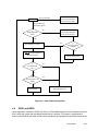
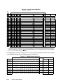
Figure 1-1. System Block Diagram ................................................................................................................. 1-3
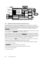
Figure 1-2. Component Block Diagram ........................................................................................................... 1-4
Figure 1-3. Internal Buffering and Data Flow ................................................................................................. 1-5
Figure 2-1. Memory Map ................................................................................................................................. 2-1
Figure 2-2. CPU to PCI Addressing Model (PREP and FPHB Modes) ........................................................... 2-2
Figure 2-3. CPU to PCI Addressing Model (CHRP Mode) .............................................................................. 2-3
Figure 2-4. Noncontiguous I/O Address Mode Enabled ................................................................................. 2-5
Figure 2-5. Address Translation Enabled in PREP Mode ............................................................................... 2-7
Figure 2-6. Address Translation Disabled in PREP Mode .............................................................................. 2-7
Figure 2-7. PCI to System Addressing Model (FPHB Mode) .......................................................................... 2-8
Figure 2-8. CHRP Address Map ..................................................................................................................... 2-9
Figure 3-1. Connection of Boot ROM and System I/O Registers to Device .................................................... 3-3
Figure 4-1. CPC710 Endian Logic .................................................................................................................. 4-2
Figure 4-2. Processor Data Bus Byte Swap for Little Endian ......................................................................... 4-5
Figure 4-3. Data Gathering Algorithm ........................................................................................................... 4-11
Figure 4-4. Deadlock avoidance circuits in the CPC710 ............................................................................... 4-14
Figure 5-1. Power Up Sequence ..................................................................................................................... 5-1
Figure 5-2. PLL Reset ..................................................................................................................................... 5-3
Figure 5-3. Arbitration to support of 4 Way Multiprocessing with the CPC710 ............................................... 5-5
Figure 6-1. DIMM Bank Configuration ............................................................................................................ 6-2
Figure 6-2. Programming with Single Bank DIMMs ........................................................................................ 6-3
Figure 6-3. Programming with Dual Bank DIMMs ........................................................................................... 6-3
Figure 6-4. SDRAM Interface Block Diagram ................................................................................................. 6-6
Figure 6-5. SDRAM Commands issued by the CPC710 ................................................................................ 6-9
Figure 6-6. Use of the CKE signal for SDRAM Control .................................................................................. 6-9
Figure 7-1. PCI Memory Read State Diagram ................................................................................................ 7-3
Figure 7-2. PCI Memory Write State Diagram ................................................................................................ 7-4
Figure 7-3. PCI Address/Data Bus for Type 0 Configuration Cycles .............................................................. 7-6
Figure 9-1. CPC710 Register Address Map ................................................................................................... 9-2
Figure 9-2. PCI Configuration Space .............................................................................................................. 9-6
Figure 10-1. Read Page Hit from PowerPC CPU to SDRAM ....................................................................... 10-1
Figure 10-2. Read Page Miss from PowerPC CPU to SDRAM .................................................................... 10-2
Figure 10-3. Write Burst Page Hit from PowerPC CPU to SDRAM .............................................................. 10-3
Figure 10-4. Write Burst Page Miss from PowerPC CPU to SDRAM ........................................................... 10-4
Figure 10-5. Write One Byte to Memory from CPU: Read Modify Write ....................................................... 10-5
Figure 10-6. Read of One Byte from the Boot ROM ..................................................................................... 10-6
Figure 10-7. Write of One Byte to the Boot Flash ......................................................................................... 10-6
Figure 10-8. Read 32 Bytes from SDRAM by a PCI Master on a 66MHz PCI64 bus: .................................. 10-7
Figure 10-9. Write 32 Bytes to SDRAM from a PCI Master on the 66MHz PCI64 bus ................................. 10-8
Figures
ix
x
CPC710 User’s Manual
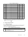
Tables
Table 4-1. Processor Little Endian Address Modification ................................................................................. 4-4
Table 4-2. Processor Little Endian Address Unmunge Equations .................................................................... 4-5
Table 4-3. Non-Burst Transactions (SYS_TBST = 1) ....................................................................................... 4-8
Table 4-4. Burst Transactions (SYS_TBST = 0) ............................................................................................... 4-9
Table 4-5. Transfer Types (Page 1 of 2)........................................................................................................... 4-9
Table 4-6. CPU Initiated Transactions (Page 1 of 5) ...................................................................................... 4-15
Table 5-1. PLL Inputs Control Signal Setting.................................................................................................... 5-2
Table 6-1. Memory Performance for Cache Line Operations (ECC Active) ..................................................... 6-1
Table 6-2. SDRAM Common Signals ............................................................................................................... 6-3
Table 6-3. External MUX Controller for Memory Data ...................................................................................... 6-4
Table 6-4. Memory Address Bit Definition for Non-Row Column Addressing Bits............................................ 6-4
Table 6-5. SDRAM Subsystem Signals ............................................................................................................ 6-4
Table 6-6. SDRAM DIMM Chip Select Connections Example.......................................................................... 6-4
Table 6-7. Supported DIMMs............................................................................................................................ 6-7
Table 6-8. SDRAM Input Signal Frequencies ................................................................................................... 6-8
Table 6-9. System Address Mapping.............................................................................................................. 6-10
Table 6-10. SDRAM Address Mapping........................................................................................................... 6-10
Table 6-11. SDRAM Control Register Programming ...................................................................................... 6-11
Table 6-12. SDRAM0_MCERx to Program Functions of DIMMs.................................................................... 6-14
Table 6-13. SDRAM0_MCERx Register Initialization ..................................................................................... 6-15
Table 6-14. ECC Check-Bit /Single-Bit Error Syndrome Matrix ...................................................................... 6-18
Table 6-15. Data Values Required for Check Bits .......................................................................................... 6-19
Table 7-1. PCI32 Bus Device Physical Connection Example ........................................................................... 7-1
Table 7-2. PCI Bus Bridge Configuration Address Map.................................................................................... 7-1
Table 7-3. Supported PCI Commands.............................................................................................................. 7-2
Table 7-4. PCI Configuration Cycle Matrix........................................................................................................ 7-5
Table 7-5. PCI to Memory Sustained Throughput ........................................................................................... 7-6
Table 7-6. CPU to PCI Sustained Throughput.................................................................................................. 7-7
Table 7-7. PCI Master Error Handling (Page 1 of 2)......................................................................................... 7-8
Table 8-1. DMA Transfer Register Summary.................................................................................................... 8-2
Table 8-2. DMA Transfer Status Cache Line Definition .................................................................................... 8-3
Table 9-1. System Registers List ...................................................................................................................... 9-3
Table 9-2. Standard PCI Configuration Registers............................................................................................. 9-7
Table 9-3. Specific PCI Host Bridge Registers ................................................................................................. 9-8
Tables
xi
xii
CPC710 User’s Manual
About This Book
This book describes the IBM CPC710 PCI bridge and memory controller, a highly integrated host
bridge device that interfaces a PowerPC 60x bus with SDRAM-based system memory and two PCI ports.
One PCI bridge supports a standard 32-bit, 33MHz PCI bus for standard and native I/O. The other PCI
bridge supports a 64-bit, 33-66MHz PCI bus for high data throughput applications such as graphics and
high-speed communications.
Who Should Use This Book
This book is for system hardware and software developers. The audience should understand
embedded processor design, embedded system design, operating systems, RISC processing, and
design for testability.
How to Use This Book
This book contains the following chapters:
“Contents”
“Figures”
“Tables”
Chapter 1, “Overview”
Chapter 2, “Addressing Model”Chapter 8, “DMA Controller”
Chapter 3, “System I/O Interface”
Chapter 4, “60x Interface”
Chapter 5, “Initialization”
Chapter 6, “Memory Controller”
Chapter 7, “PCI Bridges”
Chapter 8, “DMA Controller”
Chapter 9, “Register Summary”
Chapter 10, “Timing Diagrams”
Chapter 11, “Signal Summary”
“Index”
“Revision Log”
About This Book
xiii
Conventions and Notation
The use of overbars, for example RESET, designates signals that are active low. All signals are active high
unless shown with an overbar.
Decimal, hexadecimal, and binary numbers are used throughout this document, and are labeled as follows:
Decimal:
1234.56
Hexadecimal:
x’ABCD’
Binary:
b‘0101’
Example
Hexa
Binary
A
1010
B
1011
C
1100
D
1101
E
1110
F
1111
In Little Endian mode, bits and bytes are numbered in descending order from left to right. The most significant bit (MSB) has the highest number and the least significant bit (LSB) has the lowest number:
MSB
31
24 23
16 15
8
7
LSB
0
In Big Endian mode, bits and bytes are numbered in ascending order from left to right. The most significant bit (MSB) has the lowest number and the least significant bit (LSB) has the highest number:
MSB
0
7
8
15 16
23 24
Related Publications
The following publications contain related information:
CPC710 PCI Bridge and Memory Controller Data Sheet, SA14-2572-00
IBM PowerPC 750CX/750CXe RISC Microprocessor User’s Manual
CPC700 Memory Controller and PCI Bridge Data Sheet
CPC700 Memory Controller and PCI Bridge User’s Manual
xiv
CPC710 User’s Manual
LSB
31
Chapter 1. Overview
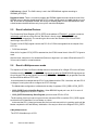
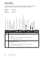
The CPC710-133 is a highly integrated host bridge device that interfaces a PowerPC 60x bus with
SDRAM-based system memory and two PCI ports. It provides arbitration for one up to four processors and
supports two levels of pipelining per processor along with 64-byte buffers.
The CPC710-133 memory controller supports SDRAM, allowing the memory to burst data on almost every
bus cycle at 100 or 133 MHz (1-1-2-1 after initial latency on Read and 1-1-1-1 on write).
For system designs requiring high I/O bandwidth, the device contains two PCI host bus bridges. One
bridge supports a standard 32-bit, 33 MHz PCI bus for standard and native I/O. The other bridge supports
a 64-bit, 33-66 MHz PCI bus for high data throughput applications such as graphics and high-speed
communications.
A DMA controller provides high speed capability for large data transfers between memory and I/O. Storegathering enhances CPU-to-I/O performance.
1.1
Features
• Up to 133 MHz PowerPC 60x 64-bit bus
• 2.5 volts 60X PowerPC bus
• Supports 100 and 133 MHz SDRAM including PC100 and PC133
• Up to 2 MB flash Boot ROM support
• 32-bit 33 MHz/64-bit 33-66 MHz async dual bus
• Reads two external 32-bit registers
• PreP and CHRP compliant design
• One-channel chained DMA controller
• Up to 256 MB Extended Flash support
• 3.3 volts ± 5%, 2.5 volts ± 2.5%
• -40 to 85°C junction temperature
• Power dissipation 2.1 watts typical at 3.3 volts - 100 MHz.
• FC-PBGA package, 729 pins, 1.27mm pitch, 35x35mm
• CMOS SA-12E, 0.25µm technology
• PLL to reduce on-chip system clock skew
• JTAG controller (LSSD design)
1.1.1
60x Bus Interface
• Supports PowerPC 750L, 750CX, 750CXe processors
• up 133 MHz external bus operation
• Supports four processors or L2 lookaside cache
• Dual 32-byte store back buffers
• High bandwidth 2-way arbiter
• Little Endian mode PowerPC
Overview
1-1
• Supports SYNC/EIEIO ordering operations
• Supports 60x bus configuration cycles
1.1.2
Memory Controller
• Supports 100 and 133 MHz SDRAM including PC100 and PC133 and Registered SDRAM
• Up to 4GB
• 2-way interleaved SDRAM with ECC
(external MUX to reduce pin count)
• Supports 16, 64, 128, and 256 Mb SDRAMs
• Programmable timing parameters
• Up to 6 dual bank DIMM
• Up to 4 banks supported for Multibanking
• SDRAM Access command queue with look ahead override option for CPU, PCI’s, and DMA
• Access based on 32-byte cache line reload
• Three separate dual 32-byte load buffers (PCI-32, PCI64, 60x)
1.1.3
PCI-32 and PCI64 Bus Bridges
• Two independent PCI bus bridges with parking
• PCI revision 2.1 compliant
• PCI32 3.3V Compliant with 5.0 V PCI signalling
• PCI64 3.3V
• Runs async logic to 60x and memory controller
• PCI64 arbitration can be disabled
• Dual 32-byte buffers in each PCI bus bridge
• Round-robin PCI arbiter
• Coherency for memory access through DMA controller or through PCI master.
• Noncontiguous byte enable transfer to memory
• The CPC710 is single load on all PCI signals
1-2
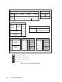
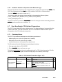
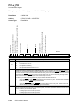
CPC710 User’s Manual
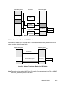
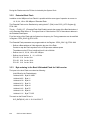
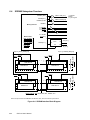
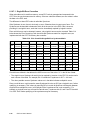
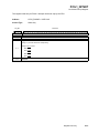
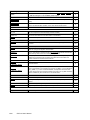
L2 Cache
L2 Cache
L2 Cache
L2 Cache
PowerPC
PowerPC
PowerPC
PowerPC
604/750L
750CX
7400
64
Optional
2nd CPU*
0
2
4
DIMM
DIMM
Optional
3rd CPU*
DIMM
Optional
4th CPU*
Up to 133 MHz
60x System Bus
2.5 Volt
CPC710-133
PCI-64 Bus, 66 MHz
DMA
72
Memory Controller
PCI Bridges
72
Pair 0
System I/O
1
3
5
DIMM
DIMM
DIMM
MUX
ECC
PCI-32 Bus, 33 MHz
72
SDRAMs, up to 4GB
xcvr
Flash
PD Regs
*The CPC710 is designed to interface with 60x system bus definition. It can also
directly interface to 1–4 PowerPC 750/7400 processors.
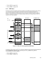
Figure 1-1. System Block Diagram
Overview
1-3
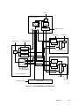
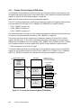
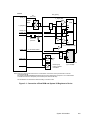
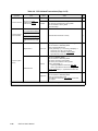
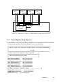
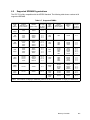
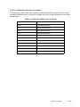
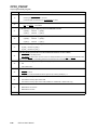
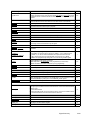
60x Bus Interface Logic
60x
Address
Queueing
Posted
Store
Buffers
Address
Decodes
Arbiter
JTAG Controller
Endian
Translation
JTAG
Interface
Configuration
Internal CPC710 Interface
Memory
DMA
PCI32
PCI64
Reset
Logic
Clock Logic
CACHE OP INTF
SDRAM
Memory
Interface
Internal CPC710 Interface
SDRAM Memory Controller
Command
Queues
ECC Correction
60X
DMA Controller Logic
PCI32
Internal CPC710 Interface
Control Logic
60x
PCI64
MEMORY PCI32
PCI64
DMA
Data Buffers
Memory
60x
PCI32
Data
Buffers
Memory
Async Boundary
PCI64
FLASH ROM
Interface
PCI Bus
Master/Slave
Logic
Internal CPC710 Interface
60x
PCI64 Bus Interface
DMA
Async Boundary
Internal CPC710 Interface
DMA
External Registers
Interface
Internal CPC710 Interface
PCI32 Bus Interface
System I/O Control
PCI Bus
Master/Slave
Logic
Data
Buffers
CPC710
Clocked at System Bus Speed
Clocked at PCI32 Bus Speed (33 MHz)
Clocked at PCI64 Bus Speed (33-66 MHz)
Dual Clocked Logic
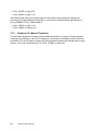
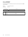
Figure 1-2. Component Block Diagram
1-4
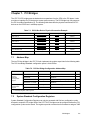
CPC710 User’s Manual
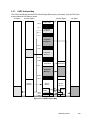
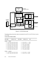
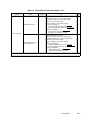
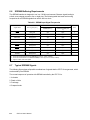
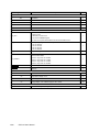
60x Bus
60x Bus Interface Logic
I/O
LE
Byte Swap
BE
LE
Byte Swap
64 Bytes
System Bus Clock
66 MHz CLK
Memory Bus
PCI64 Bus
64 Bytes
System Bus Clock
I/O
64 Bytes
S
W
A
P
64 Bytes
I/O
PCI64 Bridge Logic
64 Bytes
64 Bytes
PCI32 Bridge Logic
32 Bytes
SIO
64 Bytes
Command Queue
I/O
64 Bytes
Rotating priority:
A new arbitration
after each 32 Bytes
(Cache line=32 Bytes)
S
W
A
P
Memory Control Logic
33 MHz CLK
PCI32 Bus
System Bus Clock
DMA Controller
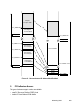
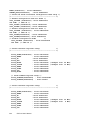
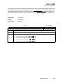
Figure 1-3. Internal Buffering and Data Flow
Overview
1-5
1-6
CPC710 User’s Manual
Chapter 2. Addressing Model
2.1
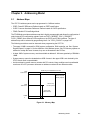
Address Maps
The CPC710 address spaces can be programmed in 3 different modes
• PREP: PowerPC REference Platform based on PREP specification
• CHRP: Common Hardware Reference Platform based on CHRP specification.
• FPHB: Flexible PCI Host Bridge Mode.
The FPHB Mode provides an address map that is highly programmable and allows for configuration of
select internal PCI configuration registers (such as PCIC1_INRESET, PCIC1_ITADDSET,
PCIC1_PSBAR) from external PCI bus agents on the PCI32 and PCI64 interfaces. The type of
address map can be selected by programming bits 0-3 of “CPC0_PGCHP” on page 9-26.
The following restrictions must be observed when programming the CPC710:
• The upper 16 MB is reserved for ROM, system configuration, DMA controller, etc. See “System
Register Space” on page 9-1 for the definition of this address space. Only PCI Memory spaces are
allowed to overlap this area. However, they are not forwarded to the PCI bus.
• At least 1MB of system memory must be available at address 0. Minimum granularity of DIMMs is
16MB.
• System memory cannot be located above 2GB. Access in the upper 2GB is not checked by the
CPC710 and result is unpredictable.
• Avoid overlapping system memory extents with PCI extents. Hang conditions and unpredictable
results can occur if a processor accesses an address contained in two different extents.
16 MB range not forwarded to PCI bus
4GB
FFFF FFFF
16 MB
Area to map PCI
Memory Spaces
2GB
7FFF FFFF
Area to map
PCI I/O spaces
Area to map
System Memory
16 MB
0
Figure 2-1. Memory Map
Addressing Model
2-1
2.2
CPU to PCI Addressing Model
2.2.1
PREP and FPHB Modes
Programmable registers described in “Specific PCI Host Bridge Registers” on page 9-8 map PCI
Memory and PCI I/O address spaces into the 4 GB System address space. Each PCI bridge in the
CPC710 contains a set of these registers, allowing firmware to program PCI address spaces
anywhere in memory rather than at fixed PCI address spaces.
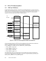
Processor View
PCI I/O Space
PCI Memory Space
4GB
4GB-16MB
Programmable Registers
PCILx_MSIZE
Peripheral
Memory Space
PCILx_SMBAR
PCI Memory
PCILx_PMBAR
PCILx_IOSIZE
Peripheral
I/O Space
PCILx_SIBAR
PCI I/O
PCILx_PIBAR
16MB
0
Figure 2-2. CPU to PCI Addressing Model (PREP and FPHB Modes)
As the above figure shows, the CPC710 monitors addresses on the processor bus to determine
whether a CPU address falls within the ranges specified by the following
PCILx_SMBAR/PCILx_MSIZE and PCILx_SIBAR/PCILx_IOSIZE registers:
• “PCILx_MSIZE” on page 9-98
• “PCILx_SMBAR” on page 9-113
• “PCILx_IOSIZE” on page 9-97
• “PCILx_SIBAR” on page 9-112
If the address falls within one of these ranges, the 60x interface logic passes the address and
command to the appropriate PCI bridge logic for execution using the translation specified by the
following PCILx_PMBAR or PCILx_PIBAR registers:
2-2
CPC710 User’s Manual
• “PCILx_PIBAR” on page 9-100
• “PCILx_PMBAR” on page 9-102
2.2.2
CHRP Mode
PCI Memory and PCI I/O address spaces are mapped into the 4GB System address space with the
use of several programmable registers contained in “Specific PCI Host Bridge Registers” on
page 9-8. These registers provide firmware a means to program PCI address spaces anywhere in
memory as opposed to having fixed PCI address spaces and each PCI bridge inside the CPC710
contains a set of these registers.
Processor View
4GB
PCI I/O Space
PCI MEMORY Space
4GB-16MB
TPM
16 MB Alias
BIM
MSIZE
PCI MEMORY
PROGRAMMABLE REGISTERS
Peripheral
Memory Space
SMBAR
BPM
TIO
IOSIZE
SIBAR
Peripheral
I/O Space
BIO
PCI I/O
PIBAR
16 MB
16 MB
0
Figure 2-3. CPU to PCI Addressing Model (CHRP Mode)
As the above Figure shows, the CPC710 will monitor addresses on the processor bus and determine
if a CPU address falls within the ranges specified by the PCILx_SMBAR/PCILx_MSIZE or
PCILx_SIBAR/PCILx_IOSIZE registers:
• “PCILx_MSIZE” on page 9-98.
• “PCILx_SMBAR” on page 9-113
Addressing Model
2-3
• “PCILx_IOSIZE” on page 9-97
• “PCILx_SIBAR” on page 9-112
If the address falls within one of these ranges, the 60x interface logic passes the address and
command to the appropriate PCI bridge logic for it to execute with the translation specified by the
PCILx_PMBAR or PCILx_PIBAR registers:
• “PCILx_PIBAR” on page 9-100
• “PCILx_PMBAR” on page 9-102
2.2.3
Peripheral I/O Address Translation
The first 8MB of Peripheral I/O space requires additional translation. To prevent 32-byte granularity
accesses to ISA addresses, the CPC710 supports a noncontiguous I/O address mode in which the
first 64KB of PCI bus I/O space is divided into 32byte segments spaced at 4K intervals within system
memory. This mode is selected by bit 5 of “PCILx_CTRLW” on page 9-92.
2-4
CPC710 User’s Manual
Peripheral
I/O Space - 8MB
PCILx_SIBAR+8MB
Area Wrapped
To First 32 Bytes
32 Bytes
PCILx_IOSIZE
PCI I/O
PCILx_PIBAR+8 MB
PCILx_IOSIZE
PCILx_SIBAR+12 KB
32 Bytes
Area Wrapped
To First 32 Bytes
Not addressable
PCILx_SIBAR+8 KB
32 Bytes
Area Wrapped
To First 32 Bytes
PCILx_SIBAR+4 KB
32 Bytes
Area Wrapped
To First 32 Bytes
32 Bytes
PCILx_SIBAR
PCILx_PIBAR + 64 KB
32 Bytes
32 Bytes
32 Bytes
32 Bytes
32 Bytes
PCILx_PIBAR
Figure 2-4. Noncontiguous I/O Address Mode Enabled
2.3
PCI to System Memory
Two types of address mapping modes are available:
• PowerPC Reference Platform (PREP) Mode
• Flexible PCI Host Bridge (FPHB) Mode.
Addressing Model
2-5
To select a mode, program bit CPC0_PGCHP[0:1] for the PCI32 or bit CPC0_PGCHP[2:3] for the
PCI64 in “CPC0_PGCHP” on page 9-26.
2.3.1
PowerPC Reference Platform (PREP) Mode
In PREP Mode, access from the PCI to the system can be performed with or without PCI address
translation. When translation is used, the most common method is to translate addresses by
complementing the upper 12 bits. PCI addresses ranging from x’8000 0000’ to x’FFFF FFFF’ are
translated to system memory addresses x’0000 0000’ to x’7FFF FFFF’.
In this mode only PCI access to Memory are decoded by the CPC710; Configuration and I/O are not
decoded.
2.3.1.1
PCI Master Address Operation
Whenever the PCI bridge logic identifies addresses coming from ISA Masters (when the
P_ISA_MASTER signal is active =1), they are passed directly to system memory. Otherwise, the
untranslated addresses are checked to determine whether they fall within a bridge’s PCI memory
address range by comparing the PCI address to the following registers:
• “PCILx_PMBAR” on page 9-102
• “PCILx_MSIZE” on page 9-98
If there is no match and if translation is enabled by software, the PCI address is translated to a system
address (bit 4 - “PCILx_PR” on page 9-104). A series of checks is performed to determine whether
the access is back to the same bridge. If it is, the PCI bridge will not respond to the PCI master.
The PCI bridge logic also forwards the access to system memory. If this address does not match a
memory configuration extent, the memory controller logic returns an invalid address error, thus
ensuring that PCI masters do not access system facilities.
2.3.1.2
Translation Enabled in PREP Mode
If translation is enabled, the PCI bridge logic translates addresses before presenting them to system
memory, as shown in the following figure. However, not all addresses are presented.
The translation is enabled by PCILx_PR[4] at address CPC0_PCIBAR + 0x000F 7F20.
2-6
CPC710 User’s Manual
System Memory Space
Translation
PCI Memory Space
4GB
Complement
Upper
Address bit(0)
2GB
Complement
Upper 12
Address Bits
No Translation
Not Forwarded
PCILx_MSIZE
PCI Memory
PCILx_PMBAR
Complement
Upper 12
Address Bits
0
Figure 2-5. Address Translation Enabled in PREP Mode
2.3.1.3
Translation Disabled in PREP Mode
If translation is disabled, the PCI bridge does not translate addresses before presenting them to the
system, as shown in the following figure.
System Memory Space
PCI Memory Space
4GB
Direct mapping
No Translation
Not Forwarded to System
PCI Memory
PCILx_MSIZE
PCILx_PMBAR
No Translation
0
Figure 2-6. Address Translation Disabled in PREP Mode
Note: Translation can be disabled for CPU-to-PCI transfers if the values stored in the PCILx_PMBAR
and PCILx_SMBAR registers are the same.
Addressing Model
2-7
2.3.2
Flexible PCI Host Bridge (FPHB) Mode
In FPHB Mode, External Masters on the 32-bit and 64-bit PCI buses address system memory using
the address translation model shown in the following figure. This model uses several programmable
registers in “Specific PCI Host Bridge Registers” on page 9-8.
Note: Each PCI bridge contains a set of programmable registers.
The CPC710 monitors addresses on the PCI bus to determine whether a PCI address falls within the
range specified by the following PCIC1_PSBAR/PCIL0_PSBAR/PCILx_PSSIZE registers:
• “PCIC1_PSBAR” on page 9-58
• “PCIL0_PSBAR” on page 9-80
• “PCILx_PPSIZE” on page 9-103
If an address falls within this range, the PCI interface logic passes the address to the 60x bridge logic
for execution using the translation specified by “PCILx_BARPS” on page 9-85.
The memory space size can be extended up to 4 GBytes by setting bit 27 of the CPC0_PGCHP
register (See page 9-27). In this case the addressing mechanism is the same as the one used for
address from 0 to 2GBytes, but it uses registers PCIC1_PPBAR, PCIL0_PPBAR, and PCIL_PPSIZE
for PCI address definition, and uses register PCIL_BARPP for base address in system memory.
• PCI64 Configuration by external PCI Agent:
This flexible FPHB mode allows the configuration by an external PCI agent of some of the CPC710
registers of the PCI 64 bus bridge such as the PCIC1_PSBAR, PCIC1_PPBAR, PCIC1_ITADDSET
and PCIC1_INTRESET registers. See “Standard PCI Configuration Registers” on page 9-6.
System Memory Space
PCI Space
4GB
Extended
System
Memory
(Optional)
(*)Memory or I/O
Space is selected by
bit 7 of PCILx_PSSIZE
Programmable
Registers
PCILx_BARPP
System
Memory
PCI Memory
or
PCI I/O (*)
PCILx_PPSIZE
PCIC1_PPBAR (PCI64)
PCIL0_PPBAR (PCI32)
PCILx_BARPS
PCI Memory
or
PCI I/O (*)
PCILx_PSSIZE
PCIC1_PSBAR (PCI64)
PCIC0_PSBAR (PCI32)
0
Figure 2-7. PCI to System Addressing Model (FPHB Mode)
2-8
CPC710 User’s Manual
2.3.3
CHRP Address Map
The PCI64 Host Bridge and the PPCI32 Host Bridge differs only by one feature: Only the PCI64 can
access Alias and Hole Memory space.
Memory Space
I/O Space
I/O Space
Memory Space
BSCA
System
Control Area
4GB
TIO 1
Peripheral
I/O Space 1
BIO 1
TIO 0
Peripheral
I/O Space 0
BIO 0
TPM 1
Peripheral
Memory 1
BPM 1
TPM 0
16 MB Alias
16 MB Alias
BIM
Peripheral
Memory 0
BPM 0
TSM 0
System
Memory
System
Memory
System
Memory
16 MB
16 MB
768KB
640 KB
BSM 0
1 MB
io- hole
processor-hole
0
Figure 2-8. CHRP Address Map
Addressing Model
2-9
2-10
CPC710 User’s Manual
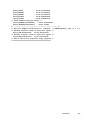
Chapter 3. System I/O Interface
The CPC710 implements a 2 MB ROM space from address 4G-2M to 4 GB and an Extended Flash of
up to 256MB.
3.1
Configuration
There is no configuration requirement for SIO logic. These areas are hard wired in the upper 16 MB of
real memory.
3.2
System I/O Registers: Application Presence Detect Bits
The device provides Output Enables signals and read cycles for two external 32-bit registers. The
read of the SDRAM0_SIOR0 or SDRAM0_SIOR1 results in a read of bits 0 to 31 of these register
which correspond respectively to the data present on the line 31 and 0 of the PCI 32 bit A/D during
the read cycle.
For descriptions of these registers, refer to:
• “SDRAM0_SIOR0” on page 9-127 controls PRES_OE0 signal
• “SDRAM0_SIOR1” on page 9-128 controls PRES_OE1 signal
• “SDRAM0_MCCR Register” on page 6-11 for the device’s supported values)
3.3
3.3.1
Flash Interface
Boot Rom
The CPC710’s Boot ROM base address is fixed at x’FFE0 0000’.
Accesses to the architected Boot ROM space within the size limit (defined in “CPC0_SIOC0” on
page 9-38) are decoded as valid Boot ROM accesses. If the ROM Size parameter is larger than the
actual amount of installed Boot ROM, the data will wrap. An access within the architected Boot ROM
space but outside the size limit (CPC0_SIOC0 x’FF00 1020’) results in a bus timeout Machine Check
error. The Boot ROM interface logic satisfies burst read requests from the processor by concatenating
multiple bytes from the Boot ROM.
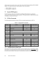
The CPC710 is designed to interface with 512 K, 1 Mb, 2Mb (x8) 3.3 V Flash memory with 80 to 120
ns access time. The following figure shows Boot Flash with the bits used for Address and Data on the
PCI32 bus AD lines. PCI AD bits 20:0 are used for Flash Address (LSB starts at bit 0).
Bits [15:8] of the PCI32 bus AD lines are used for the 8-bit data. The Boot Flash is accessed under
control of the device’s PCI32 controller to generate non-PCI cycles with FRAME not asserted. Flash
is read and written by setting bit 4 (R/W) in the CPC0_UCTL Register.
The PCI access with Frame asserted has the maximum priority. The Boot Flash or Extended Flash
access to the PCI 32 bus can be increased by setting biit 0 of the CPC0_SIOC1 Register.
System I/O Interface
3-1
During the Flash access the PCI bus is clocked by the System Clock.
3.3.2
Extended Boot Flash
In addition to the 2MBytes of boot Flash it is possible with the same type of operation to access to:
16, 32, 64, 128 or 256 MBytes of Extended Flash.
The Extended Flash can be Read/write by setting the bit 7 (R/W) in the CPC0_UCTL Register @
FF00 1000.
The pin : FLASH_CE_ (Extended Flash Chip Enable) controls the access of the Boot flash when =1
or the Extended Flash when =0. This signal is set to 0 after that the CPC710 decodes an address in
the Extended Flash Space.
For a fine tuning of the Flash and the System bus frequency, the Timing parameters can be modified
in Register: CPC0_SIOC0 @ FF00 1020.
The Extended Flash parameters are programmable in the Register: CPC0_SIOC1 @ FF00 1090
– Defines a Base address of 8 bits aligned to the size of the Flash
Permits to map the Flash anywhere in the 4 GB processor address space
The address on the PCI bus is defined from 0 Lsb to 28 Msb.
– Defines size: 16, 32, 64, 128 or 256 MBytes
– Defines size of the bus 8, 16, or 32 bits
PCI AD 15: 8 for the 8 bit
PCI AD 23:8 for the 16 bit
PCI AD 31:0 for the 32 bit
3.3.3
Byte ordering in the Boot & Extended Flash for 8 bit bus size:
The bytes in the boot Flash are ordered as following:
(Add Offset for the Flash address)
Address b'000
Byte 00 MSB
Address b'001
Byte 11
Address b'010
Byte 22
Address b'011
Byte 33
Address b'100
Byte 44
Address b'101
Byte 55
Address b'110
Byte 66
Address b'111
Byte 77 LSB
The result on the PowerPC bus is:
SYS_DATA[0:63] = 00 11 22 33 44 55 66 77
3-2
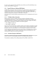
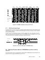
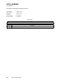
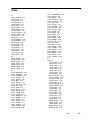
CPC710 User’s Manual
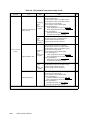
CPC710
XCVR_RD
SIO_D[15:8]
Dir
(see note)
F_AD[19] Msb
PCI32
BUS
CE
DATA
P_ADL[31:0]
B side
A side
F_AD[18:0]
REG
ADD
WE
OE
LVT245
XADR_LAT
FLASH_OE
OE
FLASH_WE
WE
Strap for
Flash write
protection
CE
VCC
F_AD[18:0]
ADD
512 K x 8 BOOT FLASH
FLASH_CE
=1 Boot Flash Enable
BCT245
CE
ADD
F_AD[28:0]
REG
PRES_OE1
REG1
PRES_OE0
REG0
PDbits 0
[0:31]
OE
WE
PDbits 1[0:31]
Presence Detect:
8 bits/Bank
EXTENDED FLASH
(up to 256 MB)
Note: There is no output enable control for the LVT245 drivers. All control is done by the Direction control bit
on signal XCVR_RD
For a Read of the Boot ROM/Extended Flash data, the XCVR_RD signal is at Up level =1 such that the Data
is transferred from the A Side (Flash) to the B Side (CPC710 PCI32 AD bus).
The 245 Buffer is recommended to limit the loading on the PCI 32 bus.
Figure 3-1. Connection of Boot ROM and System I/O Registers to Device
System I/O Interface
3-3
3-4
CPC710 User’s Manual
Chapter 4. 60x Interface
The 60x interface ties the CPC710 to the PowerPC 60x system bus. It performs the following
functions:
• Arbitration
• Configuration
• Processor load/store address decoding
• PCI to Memory access Snoop operations
• Sync/EIEIO processing
• Endian translation
• Reset logic operations
• Time base functions
4.1
Endian Support
The Data in a system built with the CPC710 are in the following mode:
• System Memory: Big Endian
• PCI space: Little Endian (Bytes are always swapped inside the CPC710)
• PowerPC Processor Big Endian.
However, the Little Endian mode is also supported for the processor but the CPC710 internally swap
bytes and unmundge address before sending it to the memory or the PCI bus.
60x Interface
4-1
PowerPC
CPU
60x BUS
Big Endian
(Little Endian option)
Address
Data
PCI64 Bridge Logic
Unmunge and
Byte Swap
(Little Endian On)
Big Endian
Memory
64 Bytes
Data Buffers
Byte
Swap
PCI64 BUS
PCI32 Bridge Logic
Byte
Swap
Address
Memory
Control
64
64
Bytes
Buffer
64
Bytes
Buffer
32
Bytes
Buffer
Data
PCI32 BUS
SIO
ROM
Little Endian
CPC710
Figure 4-1. CPC710 Endian Logic
The following listing shows how the data are transmitted from the CPU to the PCI32 bus for various
size of bytes.
Access CPU to PCI32 in Write
=========================================================================
CPU Addr
data[0:63]
PCI Addr
data[31:0]
BE
=========================================================================
TSIZE = 1 Byte
0 11 00 00 00 00 00 00 00
0 00 00 00 11
1110
1 00 11 00 00 00 00 00 00
0 00 00 11 00
1101
2 00 00 11 00 00 00 00 00
0 00 11 00 00 1011
3 00 00 00 11 00 00 00 00
0 11 00 00 00 0111
4 00 00 00 00 11 00 00 00
4 00 00 00 11 1110
5 00 00 00 00 00 11 00 00
4 00 00 11 00 1101
6 00 00 00 00 00 00 11 00
4 00 11 00 00 1011
7 00 00 00 00 00 00 00 11
4 11 00 00 00 0111
TSIZE = 2 Bytes
0 11 22 00 00 00 00 00 00
1 00 11 22 00 00 00 00 00
4-2
CPC710 User’s Manual
0
0
00 00 22 11
00 22 11 00
1100
1001
2
3
00 00 11 22 00 00 00 00
00 00 00 11 22 00 00 00 BURST
4
5
6
00 00 00 00 11 22 00 00
00 00 00 00 00 11 22 00
00 00 00 00 00 00 11 22
TSIZE
0
1
2
= 3 Bytes
11 22 33 00 00 00 00 00
00 11 22 33 00 00 00 00
00 00 11 22 33 00 00 00 BURST
3
00 00 00 11 22 33 00 00 BURST
4
5
00 00 00 00 11 22 33 00
00 00 00 00 00 11 22 33
TSIZE = 4 Bytes
0 11 22 33 44 00 00 00 00
1 00 11 22 33 44 00 00 00 BURST
2
00 00 11 22 33 44 00 00 BURST
3
00 00 00 11 22 33 44 00 BURST
4
00 00 00 00 11 22 33 44
TSIZE = 5 Bytes
0 11 22 33 44 55 00 00 00 BURST
1
00 11 22 33 44 55 00 00 BURST
2
00 00 11 22 33 44 55 00 BURST
3
00 00 00 11 22 33 44 55 BURST
TSIZE = 6 Bytes
0 11 22 33 44 55 66 00 00 BURST
1
00 11 22 33 44 55 66 00 BURST
2
00 00 11 22 33 44 55 66 BURST
TSIZE = 7 Bytes
0 11 22 33 44 55 66 77 00 BURST
1
00 11 22 33 44 55 66 77 BURST
0
0
4
4
4
4
22
11
00
00
00
22
11
00
00
00
22
11
00
00
00
22
11
00
00
00
22
11
00
00
0011
0111
1110
1100
1001
0011
0
0
0
4
0
4
4
4
00
33
22
00
11
00
00
33
33
22
11
00
00
00
33
22
22
11
00
00
00
33
22
11
11
00
00
33
00
22
11
00
1000
0001
0011
1110
0111
1100
1000
0001
0
0
4
0
4
0
4
4
44
33
00
22
00
11
00
44
33
22
00
11
00
00
44
33
22
11
00
00
44
00
33
22
11
00
44
00
33
00
22
11
0000
0001
1110
0011
1100
0111
1000
0000
0
4
0
4
0
4
0
4
44
00
33
00
22
00
11
55
33
00
22
00
11
55
00
44
22
00
11
55
00
44
00
33
11
55
00
44
00
33
00
22
0000
1110
0001
1100
0011
1000
0111
1000
0
4
0
4
0
4
44
00
33
00
22
66
33
00
22
66
11
55
22
66
11
55
00
44
11
55
00
44
00
33
0000
1100
0001
1000
0011
0000
0
4
0
4
44
00
33
77
33
77
22
66
22
66
11
55
11
55
00
44
0000
1000
0001
0000
60x Interface
4-3
TSIZE = 8 Bytes
0 11 22 33 44 55 66 77 88 BURST
0 44 33 22 11 0000
4 88 77 66 55 0000
=========================================================================
4.1.1
PowerPC Processor Behavior Mode
The CPC710 supports PowerPC 604 and 750 processors operating in Big Endian (BE) and Little
Endian (LE) modes. The mode determines the order in which a multibyte scalar is stored in memory
or I/O. In BE mode, the specified address contains the scalar’s most significant byte (MSB), the next
sequential address contains the second MSB, and so on. In LE mode, the specified address contains
the scalar’s least significant byte (LSB), the next sequential address contains the second LSB, and so
on.
4.1.1.1
Processor Behavior in LE Mode
PowerPC 604 and 750 processors normally operate in BE mode. To operate in LE mode, the
processors generate an LE address internally and then modify, or “munge,” the three low-order
address bits to create a BE address equivalent. The processors do not issue unaligned LE transfers
on the bus. Instead, they take an alignment interrupt. However, the PowerPC 604+ processor does
issue unaligned LE transfers as long as they do not cross word boundaries. The following table
describes the addresses generated by the processor for LE transfers.
4.1.1.2
Endian Behavior
PREP architecture requires data to be stored in the same Endian mode as the processor. Therefore,
the CPC710 implements logic to “unmunge” the address and byte swap the data bus as it comes from
the processor before sending it to memory or to the PCI bridges. See CPC710 Endian Logic shown
previously.
Table 4-1. Processor Little Endian Address Modification
Transfer Size (bytes)
Processor’s Internally
Generated LE Effective Address
[29:31]
1
2
3
1
4
52
62
72
8
Resulting Processor Big-endian Address [29:31]
0
7
6
53
1
6
53
43
2
5
4
3
4
4
3
2
13
5
2
13
03
6
1
0
7
0
4
0
1. The PowerPC 604+ does not support 3-byte transfers in LE mode, however, these transfer sizes will result from an
unaligned 4-byte access to an odd address
2. These transfer sizes are not supported by any of the processors.
3. These cells apply only to the PowerPC 604+ which performs unaligned LE transfers.
4-4
CPC710 User’s Manual
0
Because the CPC710 cannot determine the processor’s Endian state, software must write to the
Arbiter Control Register (bit 9) at the same time the processor HID register bit is updated. If the
processor is operating in BE mode, bit 9 must be set to 0 to prevent the CPC710 from unmunging or
byte swapping the processor’s data. If the processor is operating in LE mode, bit 9 must be set to 1 to
unmunge the address as specified in Processor Little Endian Address Unmunge Equations below,
and to swap the data bus bytes as specified in Processor Data Bus Byte Swap for Little Endian below.
Table 4-2. Processor Little Endian Address Unmunge Equations
Transfer Size
Equation to Convert to Address
1 Byte
ADDR[29:31] XOR ‘111’
2 Byte
ADDR[29:31] XOR ‘110’ and ‘1(31)1’
3 Byte
ADDR[29:31] XOR ‘101’
4 Byte
ADDR[29:31] XOR ‘100’
8 Byte
none
Byte 0
Byte 1
A
60x Data Bus
0
B
78
Byte 0
0
23 24
F
E
23 24
Byte 5
E
31
Byte 3
15 16
Byte 4
D
Byte 2
G
78
Byte 3
C
15 16
Byte 1
H
Internal
Data Bus
Byte 2
0
F
0
H
15 16
Byte 5
D
Byte 7
G
78
Byte 4
31
Byte 6
23 24
Byte 6
C
Byte 7
B
78
15 16
31
A
23 24
31
Figure 4-2. Processor Data Bus Byte Swap for Little Endian
4.2
60x Bus Arbiter Description
The arbiter in the CPC710 has the following characteristics:
• Arbitration for three devices; two levels for external masters and one for internal CPC710 requests
• No half-cycle precharge required for SYS_TA, SYS_TEA, ABB, and DBB
• Highly programmable address pipeline control
• Data streaming capability for external devices
• Programmable address bus parking capability
• Programmable timing on SYS_AACK
• Rotating address bus request priority scheme
60x Interface
4-5
4.2.1
Rotating Priority Resolution
The CPC710’s 60x arbiter implements an algorithm that rotates priorities when the address bus is
granted to a master. When multiple masters request the bus, the arbiter grants the bus to the master
with the highest priority during the arbitration period, then downgrades that priority to the lowest level
for the next period. The arbitration period occurs during the SYS_AACK assertion cycle.
If two masters continuously request the bus, they receive alternate control. This logic is satisfactory
unless a master implements a 64-byte cache line and needs to issue two 32-byte burst transfers to fill
the cache. In this case, the CPC710 has a programmable mode whereby the arbiter allows one bus
master to perform a pair of back-to-back address tenures even if another master requests the bus.
This mode allows the CPC710’s memory controller to remain in page mode for these accesses.
Without this mode, another master could insert a memory transaction to take the memory controller
out of page mode.
4.2.2
Address Bus Pipelining
Pipelining is controlled by bits 0 and 1 of the 60x Arbitration Control register (CPC0_ABCNTL).
Bit
Description
‘10’
0-1
‘01‘
‘00’
‘11’
4.2.3
4.2.3.1
If enabled by software, the arbiter maintains up to a two level pipeline per master. The arbiter continues
to grant the address bus to a specific master until there are as many as three outstanding address tenures
waiting for a data bus tenure to complete or begin. Since the CPC710 supports two masters on the system bus, there can be as many as six address tenures on the 60x system bus that have not completed or
begun a data bus tenure. The arbiter stops granting the address bus to a particular master after its third
address tenure. The CPC710 can also drive a seventh, address-only, tenure onto the bus to satisfy a
DMA snoop operation.
The arbiter maintains a one level pipeline per master. The CPC710 stops granting the address bus to a
master after it has two outstanding address tenures waiting for a data bus tenure to complete. With two
masters in the system, there could be as many as four outstanding address tenures waiting for a data bus
tenure to complete or begin, and a fifth CPC710 generated address-only tenure.
Pipelining is completely disabled. Even with two masters in the system, there will only be one address
tenure waiting for a data tenure to complete.
Implemented to accommodate slave devices like an L2 lookaside that can only support one level pipeline
regardless of the number of masters on the 60x bus.
Arbiter Requirements
Internal ABB
All devices on the 60x bus must generate an internal ABB. Because the arbiter may grant the address
bus to a requesting device while another master is active, the requesting master must generate an
ABB based on SYS_TS and SYS_AACK. The current master does not provide an ABB.
4.2.3.2
Qualified SYS_BG Equation
Use the following equation to detect a qualified bus grant using positive logic:
QBG = SYS_BG + ABB + SYS_ARTRY
where ABB represents the interval between SYS_TS and SYS_AACK active.
Bus Request (SYS_BR) need not be active to detect a qualified bus grant (parked case).
4-6
CPC710 User’s Manual
4.2.3.3
SYS_TS Assertion
All master devices must drive SYS_TS active in the cycle immediately following a qualified address
bus. Otherwise, the address tenure is aborted and another master is free to drive the address bus.
4.2.3.4
SYS_BR Negation
All master devices must negate SYS_BR for at least one bus cycle immediately after receiving a
qualified bus grant.
4.2.3.5
Qualified SYS_DBG Equation
The equation for qualified SYS_DBG using positive logic is:
QDBG = SYS_DBG + ARTRY
DBB is unused because the arbiter does not issue a SYS_DBG when DBB is active. The arbiter
monitors transaction sizes to determine the end of a data bus tenure and waits until the previous data
tenure is complete before issuing a SYS_DBG to the next master.
Note: QDGB can only be negated by an SYS_ARTRY of the address tenure associated with the QDBG
data bus tenure. Therefore, once the SYS_ARTRY window has passed for an address tenure, the
data bus tenure associated with that address tenure cannot be negated by SYS_ARTRY from a
subsequent address tenure.
4.2.3.6
High Impedance After SYS_TEA
Masters and slaves must execute all data bus signals as high impedance within two bus clocks from
SYS_TEA assertion.
4.2.3.7
SYS_DRTRY Assertion
Slaves are not allowed to drive SYS_DRTRY active. The CPC710 arbiter does not receive
SYS_DRTRY.
4.2.3.8
Slave Data Bus Determination
To determine whether the data bus is currently in use by a previous address tenure, a slave must
sample DBB from its master during the TS active cycle. If DBB is active, the slave must wait for DBB
to go inactive in a one-level pipeline mode for at least one cycle before providing read data or
accepting write data.
4.2.3.9
SYS_L2_Hit Assertion
For the CPC710 to determine whether an addressing error has occurred, all slaves on the 60x bus
must assert SYS_L2_HIT when selected by an address on the 60x bus.
Warning: The SYS_L2_HIT signal is subject to timing constraints.
60x Interface
4-7
4.2.4
4.2.4.1
Bus Enhancements
DBB not Required by Masters
Masters do not require DBB. The arbiter does not grant the data bus to a requesting master if the bus
is currently in use. The CPC710 does not drive DBB since it acts as an address-only bus master.
4.2.4.2
Half-Cycle Precharge not Required on SYS_TA
The CPC710 can be programmed so the precharge of SYS_TA is not required. This requires all
slaves to initially drive SYS_TA active or inactive immediately following a data bus grant. At the end of
a data bus tenure, a slave does not perform a precharge, which requires a slave in the next data bus
tenure to drive SYS_TA in the first cycle of the tenure.
The CPC0_ABCNTL[13] mode bit, as described in “CPC0_ABCNTL” on page 9-10, forces the
CPC710 to do a precharge if a slave on the 60x bus does not support this function.
Half-Cycle Precharge not Required on SYS_TEA
The arbiter does not grant the data bus for two bus cycles following assertion of SYS_TEAs. This
allows a slave to perform a full cycle precharge on SYS_TEAs.
4.2.4.3
SYS_ARTRY_PREV in QDBG Equation Eliminated
When SYS_ARTRY is asserted, the arbiter negates all bus grants in the cycle following SYS_ARTRY.
This supplants the requirement for masters to qualify associated bus grants by asserting
SYS_ARTRY in a previous cycle.
4.2.5
60x Bus Transfer Types and Sizes
The following tables describe the transaction types supported by the CPC710 on the processor bus.
The CPC710 supports the PowerPC 604 critical double word burst transactions.
Table 4-3. Non-Burst Transactions (SYS_TBST = 1)
SYS_TSIZ[0:2]
A[29:31]
Definition
000
000 - 111
8-byte transfer
001
000 - 111
1-byte transfer
010
000 - 111
2-byte transfer
011
000 - 111
3-byte transfer
100
000 - 111
4-byte transfer
101
000 - 111
5-byte transfer
110
000 - 111
6-byte transfer
111
000 - 111
7-byte transfer
Note
1
1. For transfers where the number of bytes to transfer cross a doubleword boundary, the CPC710 will truncate the transfer size
to avoid crossing a doubleword boundary.
4-8
CPC710 User’s Manual
Table 4-4. Burst Transactions (SYS_TBST = 0)
SYS_TSIZ[0:2]
A[27:31]
Definition
Support
Notes
000
xxxxx
8 Byte transfer
No
2
00xxx
16-byte transfer beginning on 32-byte boundary
TBD
01xxx
16-byte transfer beginning on odd doubleword boundary
10xxx
16-byte transfer beginning on odd 16-byte boundary
11xxx
16-byte transfer beginning on odd doubleword boundary
00xxx
32-byte transfer beginning on 32-byte boundary
01xxx
32-byte transfer beginning on odd doubleword boundary
No
001
010
TBD
No
1,3
Yes
10xxx
32-byte transfer beginning on odd 16-byte boundary
1,3
11xxx
32-byte transfer beginning on odd doubleword boundary
1,3
1. For transfers that cross a 32-byte boundary, the CPC710 will wrap to the beginning of the 32-byte block to satisfy the data
transfer.
2. Unpredictable results will occur if this transfer size is attempted on the processor bus.
3. Not supported on store operations
Table 4-5. Transfer Types (Page 1 of 2)
TT[0:4]
Operation
Transaction
Support as
Master
Support as Slave
00000
Clean Sector
Address-only
Yes
NOP
00001
LARX Reservation Set
Address-only
No
NOP
00010
Write with Flush
SBW or Burst
No
Yes
00011
Reserved (arbiter will assume address-only transaction)
00100
Flush Sector
Yes
NOP
00101
Reserved (arbiter will assume address-only transaction)
00110
Write with Kill
No
Yes (treated as 00010)
00111
Reserved (arbiter will assume address-only transaction)
01000
SYNC
Address-only
No
Yes
01001
TLBSYNC
Address-only
No
Yes
01010
Read
SBR or Burst
No
Yes
01011
RWNITC - Read with no Intent to Cache
SBR or Burst
Yes (See
CPC0_ATAS Register)
Yes (treated as 01010)
01100
Kill Sector
Address-only
Yes
NOP
01101
ICBI
Address-only
No
NOP
01110
RWITM - Read with Intent to Modify
Burst
Yes (See
CPC0_ATAS Register)
Yes (treated as 01010)
No
Yes
Address-only
Burst
01111
Reserved (arbiter will assume address-only transaction)
10000
EIEIO
10001
Reserved (arbiter will assume address-only transaction)
Address-only
Note: SBW = Single Beat Write, SBR = Single Beat Read
60x Interface
4-9
Table 4-5. Transfer Types (Page 2 of 2)
TT[0:4]
Operation
Transaction
Support as
Master
Support as Slave
SBW
No
Yes (treated as 00010)
No
Yes
10010
Write with Flush Atomic
10011
Reserved (arbiter will assume address-only transaction)
10100
ECOWX - Graphics Write
SBW
10101
Reserved (arbiter will assume address-only transaction)
1011x
Address-only
11000
TLB Invalidate
11001
Reserved (arbiter will assume address-only transaction)
11010
Read Atomic
11011
Reserved (arbiter will assume address-only transaction)
11100
ECIWX - Graphics Read
11101
Reserved (arbiter will assume address-only transaction)
11110
RWITM Atomic
11111
Reserved (arbiter will assume address-only transaction)
SBR or Burst
SBR
Burst
No
No
Yes (treated as 01010)
No
Yes
No
Yes (treated as 01010)
Note: SBW = Single Beat Write, SBR = Single Beat Read
4.3
Data Gathering
The 60x logic gathers data for CPU store-transfers to the PCI bus bridges. During data gathering,
single beat stores of up to 32bytes from the CPU are gathered before being sent to the PCI bus
bridge unit. Data gathering reduces asynchronous boundary crossings and facilitates data bursting
on the PCI bus.
4-10
CPC710 User’s Manual
PCI logic went idle
Idle
If there are store buffers that
have not been transferred
to PCI, send to PCI logic
Single beat store to
PCI Memory Space
Is
address gatherable
or first?
No
If there are store buffers that
have not been transferred
to PCI, send to PCI logic
Yes
Is
there a store buffer
available?
Yes
Save address for compare
No
SYS_TA the data off 60x bus
and place in buffer
Wait for buffer to empty
Is
PCI bridge logic
busy?
No
Yes
Is this
the last location in the
buffer?
Yes
No
Reset first flag
Initiate command to send
store buffer data to PCI
Figure 4-3. Data Gathering Algorithm
4.4
SYNC and EIEIO
When a processor executes a SYNC instruction, a SYNC address-only tenure is broadcast on the 60x
bus to notify the system that a software-placed barrier is present. The system is responsible for
ensuring all previously executed load and store operations are complete and all resultant actions are
60x Interface
4-11
visible to the system. The CPC710 satisfies this requirement by SYS_ARTRYing the SYNC operation
until all of its store buffers are empty, all reads have been executed, and all data have been placed in
internal CPC710 buffers for requests issued by the same processor issuing SYNC.
When a processor broadcasts an EIEIO on the 60x bus, the system is responsible for ensuring all
previous transactions are complete before executing operations. The CPC710 does not SYS_ARTRY
the EIEIO because the 60x logic dispatches bus transactions to the logic units in the order in which
they occur on the system bus and each logic unit executes its commands in the order received. For
diagnostic purposes, the CPC710 can be programmed to SYS_ARTRY the EIEIO in the same
manner as SYNC (see bit 10 of “CPC0_ABCNTL” on page 9-10).
The logic units are system memory, PCI-32 bus bridge, PCI64 bus bridge, system I/O logic, and DMA
controller logic. EIEIO operations are valid for transfers to and from the same logic unit, but execution
order of load and store operations to different logic units cannot be guaranteed. For example, a store
to the PCI-32 bus bridge followed by a PCI64 store could be presented to the respective PCI buses in
reverse order if a bus is busy. To preserve the order among logic units, software must issue a SYNC
instead of an EIEIO.
4.5
4.5.1
Address Retry (SYS_ARTRY)
Precharging SYS_ARTRY and SYS_SHD
This function is programmable by the bit 12 of CPC0_ABCNTL register.
The CPC710 can be programmed to precharge the ARTRY_ and SHD_ signals. This requires
that all devices on the 60x bus must disable their precharge of this signal. The CPC710 negates
these signals in the second cycle following the last cycle of the ARTRY window for 1/2 of a bus
cycle
4.5.2
SYS_ARTRY Assertions
The CPC710 asserts SYS_ARTRY for:
• SYNC operations as described in the previous section
• EIEIO operations as described in the previous section
• XFERDATA when more than two transfers have been initiated
• a processor access to the PCI bus when a PCI-ISA bus bridge requests the same PCI bus
• a processor access to system memory when a DMA occurs to the same cache line
• a processor access to system memory when a DMA operation occurs to the same line
• a processor access into a range of PCI-32 or PCI64 addresses defined as potential deadlock
4.5.3
Recommended SYS_ARTRY Procedure
• A master that has had its address tenure retried should negate its SYS_BR[n] for at least one bus
cycle in the cycle immediately following detection of an active SYS_ARTRY.
• A master that has retried an address tenure due to a snoop hit should activate its SYS_BR[n] in the
cycle immediately following the detection of an active SYS_ARTRY. This ensures the master that
retries is serviced before the master that was retried.
4-12
CPC710 User’s Manual
4.6
Deadlock Avoidance
Potential Deadlock
Potential deadlock situations can occur when the CPU attempts to access (read or write) a PCI
master, while at the same time the PCI master attempts to access a cacheable main memory
address. The PCI to memory access generates a snoop cycle on the processor bus, and if that
results in a cache hit, the PCI master's memory access will get retried. If the PCI master (typically a
PCI-PCI, PCI-ISA or PCI-VME bridge) does not have enough internal buffering to support incoming
as well as outgoing transactions or uses prioritization that requires the outgoing transaction to
complete before servicing the incoming CPU's read or write, a deadlock will occur.
Deadlock Avoidance with the CPC710
There are three ways to implement deadlock avoidance:
1. For the PCI32 bus only, external logic can be used with P_MEMREQ and P_MEMACK signals (not
recommended for new designs).
2. External logic can be used with the DLK and NODLK signals (not recommended for new designs).
3. Use of CPC710 internal deadlock avoidance logic. This is the preferred solution, as it can be
managed by software. The DLK and NODLK pins may not be supported in future revisions, and
should not be used.
The internal deadlock avoidance circuit is active when at least one of the bits 0, 1, and 16 of the
CPC0_ DLKCTRL register are set to 1 and CPC0_PGCHP register bit 24 is set to 0.
For each PCI bus, there are six unique registers and one common register that are associated with
the deadlock avoidance logic.
- Internal Deadlock avoidance circuit control setup:
PCILx_DLKCTRL
PCILx_DLKDEV
- Internal Deadlock avoidance address window definition:
PCILx_TPMDLK
PCILx_BPMDLK
PCILx_TIODLK
PCILx_BIODLK
- External Deadlock signal control (common for PCI32 and PCI64)
CPC0_PGCHP[24] should be set to 0 when using the internal deadlock logic.
60x Interface
4-13
CPU
ARTRY CPU
External
Deadlock
management
circuit
(will be
in removed
future version)
DLK
PAL 1 NODLK
PAL 2
(3) Internal Deadlock
avoidance circuit
PCILx_DLKCTRL
PCILx_DLKDEV
PCILx_TPMDLK
PCILx_BPMDLK
PCILx_TIODLK
PCILx_BIODLK
CPC0_PGCHP[24]
64
PowerPC Bus
(2)with ext
Deadlock Assist
P_MEMACK
P_MEMREQ
Snoop
(1)with ext
Deadlock Assist
Memory
Controller
PCI64 Bus
66 MHz
1
2
PCI-PCI
bridge
PCI32 Bus
33 MHz
Figure 4-4. Deadlock avoidance circuits in the CPC710
4.6.1
Deadlock Avoidance Operation with Internal Logic
The Deadlock avoidance internal circuit is enabled when any one of the bits 0, 1, or 16 of the
Deadlock avoidance control register (PCILx_DLKCTRL) is set to 1. An access from the CPU to PCI
that hits in the range of addresses defined as the deadlock avoidance window (as programmed in
registers PCILx_TPMDLK, PCILx_BPMDLK, PCILx_TIODLK, PCILx_BIODLK) will generate a
SYS_ARTRY signal on the CPU bus.
For read operations that fall in the deadlock avoidance window, the CPC710 takes the CPU request
and then generates the SYS_ARTRY and performs a delayed read.
For write operations, the first write in the address window is not retried if the PCI bus is busy. If the
deadlock avoidance circuit is not programmed, the SYS_ARTRY will not appear. This is what will
happen if the PCI bus agent is smart enough to buffer its transactions in the case that resources are
not free, and allowing for a PCI retry operation to occur. If system PCI agents support this type of
operation then use of the CPC710's internal deadlock avoidance is not necessary.
For monitoring purposes, the DLK signal can be enabled (PCILx_DLKCTRL[6] = 1) and observed.
Sequence of operation with the Deadlock avoidance internal circuit
1. CPC710 detects that the CPU to PCI access is in the range of addresses defined in registers.
2. CPU to PCI access is flushed
3. SYS_ARTRY is generated on the 60X bus by the CPC710
4. Execute PCI master Read/Write access to System Memory with Snoop.
5. End of the PCI master operation
6. CPU access to the PCI
4-14
CPC710 User’s Manual
4.6.2
Deadlock Avoidance Operation with External Logic
This mode of operation requires the use of external logic to generate the CPC710 input NODLK. The
CPC710 will generate the output DLK for a CPU access to the PCI32 or PCI64 bus when:
- the input NODLK is not active (is read as a '1')
- the access is within the address window defined by the appropriate address registers
(PCILx_TPMDLK, PCILx_BPMDLK, PCILx_TIODLK, PCILx_BIODLK)
- CPC0_PGCHP[24] is set to '1'
The CPC710 will then generate a SYS_ARTRY to the CPU bus logic when the externally generated
NODLK signal becomes active (is read as a '0').
4.7
Error Handling for CPU-Initiated Transactions
The CPC710 uses Machine Checks to indicate errors. This allows software to log errors before the
system is shut down. In an MP environment, the CPC710 activates the Machine Check pin that
corresponds to the CPU initiating the transaction.
4.7.1
Checkstop Errors
The CPC710 generates a checkstop when the following are detected:
• Address parity error on the 60x system bus (if enabled)
• Data parity error on 60x system bus (if enabled)
• Internal timeout due to no response from slave on load
The 60x logic performs the following when generating a checkstop:
1. Sets appropriate bit(s) in CPC0_SESR
2. Drives CHKSTOP active until power on reset
The following table describes the error handling performed for CPU initiated transactions. The 60x
logic drives SYS_MCP0:1 signals, not the PCI bridge logic or the memory control logic.
Table 4-6. CPU Initiated Transactions (Page 1 of 5)
Operation
Access not directed
to the CPC710
Error
Addressing Error
(SYS_L2_HIT not driven
active)
Mode
Action
Disabled
No action taken
Enabled
Set No Select error bit in CPC0_SESR
Set error address in CPC0_SEAR
CPC0_PGCHP[26] = 0: Signal Machine Check with
SYS_TEA
CPC0_PGCHP[26] ≠ 0: Signal Machine Check with
SYS_MCP0:1
Note
Notes: 1. A dummy 0 is returned for read operation. For write, data is ignored.
60x Interface
4-15
Table 4-6. CPU Initiated Transactions (Page 2 of 5)
Operation
Access to CPC710
Error
Bus Time-out: Time
expired from SYS_AACK
active to first SYS_TA
Mode
Action
Disabled
Inhibit timer; no action taken
Enabled
Set bus time-out error bit in CPC0_SESR
Set checkstop generated bit in CPC0_SESR
Set error address in CPC0_SEAR
Signal Checkstop
Note
Access to a reserved or
non- implemented address
Access to internal
CPC710 facilities
Alignment or size
Terminate CPU transaction normally
Store to read-only register
Load from write-only register.
Single bit error
Access to system
memory
Don’t care
Set single-bit error and syndrome in SDRAM0_MESR
Set error address in SDRAM0_MEAR
Return corrected data to CPU
If CPC0_PGCHP[17] = 1 and CPC0_PGCHP[26] = 1:
Set memory error bit in CPC0_SESR
Set memory error address in CPC0_SEAR
Signal Machine Check with SYS_MCP0:1
Normal
Set error in SDRAM0_MESR
Set error address in SDRAM0_MEAR
Set memory error bit in CPC0_SESR
Set memory error address in CPC0_SEAR
if CPC0_PGCHP[26] = 0:
Loads: Signal Machine Check with SYS_TEA
Stores: Signal Machine Check with SYS_MCP0:1
If CPC0_PGCHP[26] = 1, signal Machine Check with
SYS_MCP0:1
Diagnostic
Set double-bit error in SDRAM0_MESR
Set error address in SDRAM0_MEAR
Return uncorrected data to CPU
Signal Machine Check with SYS_MCP0:1 if write less
than 8 bytes
Double-bit error
Notes: 1. A dummy 0 is returned for read operation. For write, data is ignored.
4-16
CPC710 User’s Manual
1
Table 4-6. CPU Initiated Transactions (Page 3 of 5)
Operation
Error
Mode
Action
Note
No DEVSEL received
Master-abort the PCI transaction
Set master-aborted bit 13 in PCI Status register
Set Devsel error bit 3 in PCILx_PLSSR register
Set PCI error bit in CPC0_SESR
Set error address in CPC0_SEAR register
If CPC0_PGCHP[26] = 0:
Loads: Signal Machine Check with SYS_TEA
Stores: Signal Machine Check with SYS_MCP0:1
If CPC0_PGCHP[26] = 1:
Signal Machine Check with SYS_MCP0:1
Terminate CPU transaction normally
1
Detected SERR active during PCI transaction
Master-abort the PCI transaction
Set master aborted bit 13 in PCI Status register
Set SERR detected error in PCILx_PLSSR register
Set PCI error bit in CPC0_SESR
Set error address in CPC0_SEAR register
If CPC0_PGCHP[26] = 0:
Loads: Signal Machine Check with SYS_TEA
Stores: Signal Machine Check with SYS_MCP0:1
If CPC0_PGCHP[26] = 1:
Signal Machine Check with SYS_MCP0:1
Terminate CPU transaction normally
1
Access to PCI bus
Notes: 1. A dummy 0 is returned for read operation. For write, data is ignored.
60x Interface
4-17
Table 4-6. CPU Initiated Transactions (Page 4 of 5)
Operation
Error
Detected PCI bus data parity error on load
Access to PCI bus
(cont’d)
Mode
Enabled by
bit 6 in
PCI
PCICx_CM
D register
Continue transfer on PCI bus to completion
Activate the PERR signal
Set data parity error bit 8 in PCI Status register
Set data parity error bit 15 in PCI Status register
Set PCI error bit in CPC0_SESR
Set error address in CPC0_SEAR register
If CPC0_PGCHP[26] = 0:
Loads: Signal Machine Check with SYS_TEA
Stores: Signal Machine Check with SYS_MCP0:1
If CPC0_PGCHP[26] = 1:
Signal Machine Check with SYS_MCP0:1
Terminate CPU transaction normally
Disabled by
bit 6 in
PCI
PCICx_CM
D register.
Set parity error bit 15 in PCI Status register
Proceed normally with PCI transaction
Proceed normally with CPU transaction
Enabled by
bit 6 in
PCI
PCICx_CM
D register
Continue transfer on PCI bus to completion
Set data parity error bit 8 in PCI Status register
Set data parity error bit 15 in PCI Status register
Set PCI error bit in CPC0_SESR
Set error address in CPC0_SEAR register
If CPC0_PGCHP[26] = 0:
Loads: Signal Machine Check with SYS_TEA
Stores: Signal Machine Check with SYS_MCP0:1
If CPC0_PGCHP[26] = 1:
Signal Machine Check with SYS_MCP0:1
Terminate CPU transaction normally
Disabled by
bit 6 in
PCI
PCICx_CM
D register
Set data parity error bit 15 in PCI Status register
Proceed normally with PCI transaction
Proceed normally with CPU transaction
Detected PERR on store
Detected target abort
Action
Set received target abort bit in PCI Status register
Set PCI error bit in CPC0_SESR
Set error address in CPC0_SEAR register
If CPC0_PGCHP[26] = 0:
Loads: Signal Machine Check with SYS_TEA
Stores: Signal Machine Check with SYS_MCP0:1
If CPC0_PGCHP[26] = 1:
Signal Machine Check with SYS_MCP0:1
Terminate CPU transaction normally
Notes: 1. A dummy 0 is returned for read operation. For write, data is ignored.
4-18
CPC710 User’s Manual
Note
1
1
1
Table 4-6. CPU Initiated Transactions (Page 5 of 5)
Operation
Error
PCI Bus timeout:
P/G_TRDY count expired
Mode
Note
Enabled
Master-abort the PCI transaction
Set master aborted bit 13 PCI Status register
Set PCI bus time-out error in PCILx_PLSSR register
Set PCI error bit in CPC0_SESR
Set error address in CPC0_SEAR register
If CPC0_PGCHP[26] = 0:
Loads: Signal Machine Check with SYS_TEA
Stores: Signal Machine Check with SYS_MCP0:1
If CPC0_PGCHP[26] = 1:
Signal Machine Check with SYS_MCP0:1
Terminate CPU transaction normally
1
Enabled
Stop retrying PCI transfer
Set retry count expired bit in PCILx_PLSSR register
Set PCI error bit is CPC0_SESR
Set error address in CPC0_SEAR register
If CPC0_PGCHP[26] = 0:
Loads: Signal Machine Check with SYS_TEA
Stores: Signal Machine Check with SYS_MCP0:1
If CPC0_PGCHP[26] = 1:
Signal Machine Check with SYS_MCP0:1
Terminate CPU transaction normally
1
Access to PCI bus
(cont’d)
Retry count expired
Action
Notes: 1. A dummy 0 is returned for read operation. For write, data is ignored.
60x Interface
4-19
4-20
CPC710 User’s Manual
Chapter 5. Initialization
5.1
CPC710 Power Up Sequence:
• time= - 100 mS
- All PLL inputs are stable and at their final values: (See following recommended setting for PLL _TUNE and PLL_RANGE input signals)
- SYS_CLK is stable at or below the target frequency
- VDDA and Vdd (supply) are at their final values
- POWERGOOD input is de-asserted Low for Reset.
- PLL_RESET input is asserted active (Low).
- PCI clocks inputs (PCI_CLK and PCG_CLK) are stable at the target frequency
• time= 0
- PLL_RESET input is de-asserted inactive (High).
- PLL_LOCK output goes down up to the time that clock are locked to the PLL,
then is asserted active (High), indicating the PLL is locked.
• time= 500 µs minimum
-
POWERGOOD input is asserted (High).
HRESET output de-asserted by the CPC710 (High)
Bus transactions may begin.
Boot can begin.
Note 1: Chip reset is only controlled by the SYS_CLK.
SYS_CLK
> 100 mS
PLL_RESET (In)
T lock < 500 uS
PLL_LOCK(Out)
> 500 uS for PLL Lock
POWERGOOD(In)
Boot CPU
SYS_HRESET(Out)
G_RST/P_RST(Out)
Register Initialization
PCI 64 & 32 bus in Reset
PCILx_CRR[0]=0
T= 0
Boot
Code
Start
PCILx_CRR[0]=1
T1 Sys
Sys
Reg 500us Reg
PCI
Reg
T2 PCI
500us Slots
Config
SDRAM
Init
CPC0_RSTR[2:3]=11
CPC0_RSTR[2:3]=00
PCI Internal circuits of the CPC710 are in Reset
Figure 5-1. Power Up Sequence
5.2
POWERGOOD Power-On Reset
Using the system Power-On Reset POWERGOOD signal, the device resets internally and generates
a reset signal to all CPUs and I/O devices. All device I/O pins go to tri-state. After a POWERGOOD
Initialization
5-1
cycle, outputs on all interfaces are either floating or driven to their inactive state, except for the reset
signals sent to the board as described below.
1. PowerPC bus: HRESET0 and HRESET1 are driven Low for the same duration as the
POWERGOOD active pulse (low level).
2. PCI64 bus: G_RST is driven Low from the beginning of the POWERGOOD assertion and remains
active after POWERGOOD is deasserted. G_RST is deactivated when the processor writes a 1
into bit 0 of “PCILx_CRR” on page 9-90 - CPC0_PCIBAR + x’000F 7EF0’ for PCI64. G_RST is
deactivated within a period that complies with the PCI Specification [2] for the 64-bit interface.
3. PCI32 bus: P_RST is driven Low from the beginning of the POWERGOOD assertion and remains
active after POWERGOOD is deasserted. P_RST is deactivated when the processor writes a 1
into bit 0 of “PCILx_CRR” on page 9-90 - CPC0_PCIBAR + x’000F 7EF0’ for PCI32 after several
PCI clocks
5.3
PLL for Clock System
Recommended PLL input controls setting:
For proper PLL operation it is recommended to set the PLL input control signals as shown in
Table 5-1.
It is also recommended that the tuning bit inputs be accessible and programmable on the system
board, to permit the use of other combinations in the case of difficulties to lock the PLL. This can
adapted to conditions in the system environment.
Table 5-1. PLL Inputs Control Signal Setting
PLL_RANGE[1:0]
PLL Frequency range selector
for the System Clock
PLL_TUNE[5:0]
Loop stability
tuning control of the PLL
00
50 MHz to 100 MHz
010101
50 MHz to 100 MHz
01
58 MHz to 114 MHz
010011
58 MHz to 114 MHz
10
66 MHz to 134 MHz
010011
66 MHz to 134 MHz
11
80 MHz to 160 MHz
010011
80 MHz to 160 MHz
PLL_VDDA:
VDDA is the voltage supply pin to the analog circuits in the PLL. Noise on VDDA will cause phase
jitter at the output of the PLL. To provide isolation from the noisy internal digital Vdd signal, VDDA is
brought to a package pin. If little noise is expected at the board level, then VDDA can be connected
directly to the digital Vdd plane. In most circumstances, however, it is prudent to place a filter circuit
on VDDA as shown below. All wire lengths should be kept as short as possible to minimize coupling
from other signals.
The impedance of the ferrite bead should be much greater than that of the capacitor at frequencies
where noise is expected. Many applications have found that a resistor instead of a ferrite bead does a
5-2
CPC710 User’s Manual
better job of reducing jitter. The resistor should be kept to a value lower than 10 Ohms.
Experimentation is the best way to determine the optimal filter design for a specific application.
FB = Murata BLM31A700S or equivalent
or resistor below 10 Ω
Digital Vdd
(via at board)
2.3 to 2.7 V
Bypass
PLL_VDDA (to PLL)
C = 0.1 µF
Filter
GND
SYS_CLK
PLL_LOCK
PLL_RESET
Buffer
Phase
Detect
Charg
Pump
VCO
Div
MUX
Clock
to internal
circuits
TUNE[5:0]
PLL_TUNE[5:0]
PLL_RANGE[1:0]
CPC710-133
Figure 5-2. PLL Reset
The RESET signal serves two purposes. First, it holds the PLL in a reset state by forcing the VCO to
operate at its minimum frequency. Second, it puts the PLL in bypass mode such that PLL Output will
be buffered versions of Input SYS_Clock. RESET should be held active (high) during power-on until
all of the following condition are met:
(1)
(2)
(3)
(4)
All PLL inputs are stable and at their final values.
SYS_CLK is stable at or below the target frequency.
Any gating in the feedback path is removed.
VDDA and Vdd are at their final values.
Failure to hold the PLL in reset (RESET=high) during power-on may result in VCO run-away. In this
mode, output clocks are not present and the PLL can be recovered only by pulsing the RESET or
VDDA pins.
5.4
Initialization of the SDRAM
To Initialize the SDRAM during the system boot it is necessary to first set all the registers of the
CPC710 Memory controller and then start an automatic initialization phase by programming bit 0 of
the SDRAM0_MCCR (Memory Controller Control Register).
The MRS (Mode Register Set) cycle runs only when CPC710 register SDRAM0_MCCR bit 0 is set.
In the initialization phase, the CPC710 executes the following sequence:
1. Pause 200 µs
2. Precharge-all cycle
3. 8 refresh cycles
4. MRS cycle
When the initialization phase is completed, the bit 2 of the SDRAM0_MCCR register is set to 1, such
that a polling of this bit, permits to go ahead with the initialization of the others features of the
CPC710.
• Examples of Programming type of SDRAM
Initialization
5-3
CAS Latency = 2 or 3 The CAS Latency is set in the SDRAM Mode register according to
SDRAM0_MCCR[24].
Registered mode: There is no need to program the SDRAM registered mode, because most of the
SDRAM memory interface signal works with 2 CPU cycles, which permits to handle signals on cycle
late. In the case of Registered SDRAM, the timings on Reading data from the SDRAM will be more
critical because the data will have only one cycle to reach the Multiplexor.
5.5
Reset Individual Devices
The Connectivity Reset Register (CPC0_RSTR) at the address x‘FF00 0010’ provides a means to
individually reset devices on the 60x bus. Bits 0 and 1 directly control SYS_HRESET0 and
SYS_HRESET1 respectively. The remaining two bits control and Reset the PCI-32 and PCI64
internal logic of the CPC710.
The bits 0 of the CCR[0] register controls the PCI-32 or PCI64 reset signals that are outputs of the
CPC710.
• PCI32 bus example:
When bit 2 of register CPC0_RSTR is asserted low, the PCI32 internal circuit of the CPC710 goes to
reset.
After the reset, when the bit 2 is deasserted (Returns to high level =1) it takes 250ns before the PCI
32 bus can be used for normal accesses.
5.6
Reset in Multiprocessor mode
The sequence of Power-On Reset in Multiprocessor is the same as for a Single CPU on the 60X bus.
Simultaneously the HRESET0 and HRESET1 signal goes up after the POWERGOOD signal goes up.
One of the two CPU get the PowerPC bus through SYS_BR0 or SYS_BR1 and get granted to access
the Boot ROM at address FFFF 0100.
It can be decided for example that the CPU 0 is the Master and the CPU 1 the slave, with the CPU 0
in charge of running the code to configure the CPC710 bridge.
The Master/slave configuration is defined with the help of registers CPC0_PIDR & CPC0_RSTR
• CPC0_PIDR Physical Identifier Register: When BR0-BG0 signal pair is set, bit 31 is set to 0
BR1-BG1 signal pair is set, bit 31 is set to 1
• CPC0_RSTR Connectivity Reset Register; permit to reset CPU0 or CPU1
The first action of the boot code is to permit to the connected CPU to read the CPC0_PIDR register
such that this CPU identifies if he is a Master or a slave.
In the case the CPU 1 (slave) get access first, the boot code can put him in a pooling mode until the
Master complete the I/O and Memory initialization. One way is to write in the Register CPC0_RSTR.
4 Way Multiprocessor
The CPC710 handles up to 4 CPU.
5-4
CPC710 User’s Manual
PowerPC750CX
CPU 0
PowerPC750CX
CPU 1
PowerPC750CX
CPU 2
PowerPC750CX
CPU 3
BR0 BG0
BR1 BG1
BR2 BG2
BR3 BG3
BR0
BG0
BR1
BG1
60X Bus Arbitration
BR2
BR3
CPC710-133
4 way SMP
Figure 5-3. Arbitration to support of 4 Way Multiprocessing with the CPC710
5.7
Typical Register Setup Sequence
Many deviations from the proposed following example of set up are possible. However, it is important
to keep the basic operations in the same sequence order as described below.
/*********************************************************************/
/* Typical CPC710-100 registers setup sequence (from model simulation*/
/*
*/
/*
11/17/99
/*********************************************************************/
/* Begin CPC710-100 registers setup sequence
*/
/*=================================================*/
/* 60X Interface registers setup
*/
/* ----------------------------------------------- */
CPC0_RSTR(0xff000010) : write 0xf0000000
CPC0_UCTL(0xff001000) : write 0x32f80000
CPC0_ABCNTL(0xff001030): write 0xb0000000
CPC0_ERRC(0xff001050) : write 0x00c00000
CPC0_SESR(0xff001060) : write 0x00000000
CPC0_SEAR(0xff001070) : write 0x00000000
CPC0_PGCHP(0xff001100) : write 0x00000000
/* Memory Interface registers setup
*/
/* --------------------------------------------------- */
SDRAM0_MESR(0xff001220) : write 0x00000000
SDRAM0_MEAR(0xff001230) : write 0x00000000
MCER0(0xff001300) : write 0x800080c0
Initialization
*/
5-5
MCER1(0xff001310) : write 0x808080c0
SDRAM0_MCCR(0xff001200) : write 0x83b06000
/* PCI64 and PCI32 Interfaces Configuration mode setup */
/* ------------------------------------------------- */
/* Enable configuration mode for PCI64 */
CPC0_PCICNFR (0xff00000c): write 0x80000003
CPU SYNC /* SYNC OP */
CPC0_PCIBAR (0xff200018): write 0xff400000
CPC0_PCIENB (0xff201000): write 0x80000000
/* Enable configuration mode for PCI32 */
CPC0_PCICNFR (0xff00000c) : write 0x80000002
CPU SYNC /* SYNC OP */
CPC0_PCIBAR(0xff200018) : write 0xff500000
CPC0_PCIENB(0xff201000): write 0x80000000
/* Disable configuration modes
*/
CPC0_PCICNFR (0xff00000c) : write 0x00000000
CPU SYNC /* SYNC OP */
/* PCI64 Interface registers setup
*/
/* ------------------------------------------------- */
PCILx_PIBAR(0xff4f7800) : write 0x5c000000
PCILx_PMBAR
: write 0x5a000000
PCILx_PR
: write 0x00008000
PCILx_ACR
: write 0xff000000
PCILx_MSIZE
: write 0xfc000000
PCILx_IOSIZE
: write 0xff000000
PCILx_SMBAR
: write 0xe0000000
PCILx_SIBAR
: write 0x90000000
PCILx_CSR
: write 0x00000000
PCILx_PLSSR
: write 0x00000000
/*example with
/*example with
64 MB*/
16 MB*/
/* PCI64 Command register setup */
PCILx_CFGADDR(0xff4f8000) : write 0x04000080
PCILx_CFGDATA(0xff4f8010) : write 0x5601
/* PCI32 Interface registers setup
*/
/* ------------------------------------------------- */
PCILx_PIBAR(0xff5f7800) : write 0x1c000000
PCILx_PMBAR
: write 0x1a000000
PCILx_PR
: write 0x0000c000
PCILx_ACR
: write 0xfe000000
PCILx_MSIZE
: write 0xfe000000
PCILx_IOSIZE
: write 0xff800000
PCILx_SMBAR
: write 0xc0000000
PCILx_SIBAR
: write 0x80000000
PCILx_CSR
: write 0x00000000
5-6
CPC710 User’s Manual
/*example with
/*example with
32 MB*/
8 MB*/
PCILx_PLSSR
: write 0x00000000
PCILx_BPMDLK
: write 0xc0400000
PCILx_TPMDLK
: write 0xc0800000
PCILx_BIODLK
: write 0x80400000
PCILx_TIODLK
: write 0x80800000
/* PCI32 Command register setup */
PCILx_CFGADDR(0xff5f8000) : write 0x04000080
PCILx_CFGDATA(0xff5f8010) : write 0x5601
/* ------------------------------------------------- */
/* Wait for SDRAM initialization is complete --> SDRAM0_MCCR(2) goes to a 1 */
/* Release external reset to PCI32 bus agents */
PCILx_CRR(0xff5f7ef0) : write 0xfc000000
/* Release external reset to PCI64 bus agents */
PCILx_CRR(0xff4f7ef0) : write 0xfc000000
/* End of CPC710-100 registers setup sequence */
/*=========================================*/
Initialization
5-7
5-8
CPC710 User’s Manual
Chapter 6. Memory Controller
6.1
Overview
The CPC710 memory controller controls processor and I/O interactions with the memory system. The
memory controller supports SDRAM and is 2-way interleaved to allow the memory to burst data on
every CPU bus cycle at 133 MHz (1-1-2-1 after initial latency) using only one memory address bus. To
handle critical word load, individual control of the LSB column address bits is required for the DIMM
pair. This interleaved implementation allows the CPC710’s memory controller to run all the memory
control (except SDCKE and SDCS_) and address signals at half the System Frequency. The Data
signals between the Multiplexors and the SDRAM also run at half the 60x-bus frequency. This is a
main advantage for the board designer, allowing Time-Of-Fly for those signals up to 1 system cycle.
The CPC710-133 supports buffered, unbuffered and "Registered" SDRAM DIMMs.
The controller supports up to six dual DIMMs banks of interleaved 72-bit memory (64-bit Data + 8-bit
ECC). To reduce pin count, the controller requires a Texas Instruments (TI) ALVCH162268 MUX or
alternative IDT MUX to externally multiplex the 144-bit data to 72-bits for device input. Programmable
parameters allow a variety of memory organizations and timings.
ECC protection is provided for all 64 bits of the data bus, detecting and correcting single- and doublebit errors.
Programmable parameters allow for a variety of memory organizations (“SDRAM Subsystem
Overview” on page 6-6) and different kind of SDRAM organizations can be mixed.
The SDRAM must comply with the following requirements (compatible with the PC133
Specification [1]).
• CAS Latency = 2 or 3
• Burst length = 2
• Maximum tRCDmin allowed is 2 or 3 Clock cycles.
• Maximum tRPmin allowed is 2 or 3 Clock cycles.
• Maximum tRASmin allowed is 5 or 6 Clock cycles.
Table 6-1. Memory Performance for Cache Line Operations (ECC Active)
Pipeline
Levels
CAS Latency = 2
CAS Latency = 3
133 MHz
133 MHz
Operation
Initial
Read Burst
212 MB/s
16-1-2-1
193 MB/s
18-1-2-1
Page Hit
532 MB/s
4-1-2-1
426 MB/s
6-1-2-1
Page Miss
304 MB/s
10-1-2-1
266 MB/s
12-1-2-1
709 MB/s
3-1-1-1
709 MB/s
3-1-1-1
Page Hit
532 MB/s
5-1-1-1
532 MB/s
5-1-1-1
Page Miss
355 MB/s
9-1-1-1
355 MB/s
9-1-1-1
Sustained
2
Initial
Write Burst
Sustained
Memory Controller
6-1
6.2
Bank Definitions
The term "bank" can have several meanings, depending on context:
1. SDRAM banks
2. DIMM banks
3. Interleaved banks
6.2.1
SDRAM Banks
As shown in the following diagram, SDRAMs contain memory arranged in two or four banks. The
memory controller selects these banks using bank select (BS) address pins.
6.2.2
DIMM Banks
As shown in the following diagram, DIMMs are available in single bank and dual bank configurations.
Single Bank DIMM
Dual Bank DIMM
SDRAM Chip
Nothing on side B
DIMM
DIMM
These 5 chips
constitute
DIMM Bank A
These 5 chips
constitute
DIMM Bank A
These 5 chips
constitute
DIMM Bank B
Bank Physical Representation
DIMM Bank B
DIMM Bank A
DIMM Bank A
Schematic Representation
Schematic Representation
Figure 6-1. DIMM Bank Configuration
6.2.3
Interleaved Banks
An Interleaved Bank consists of two interleaved DIMM Banks. The two DIMM Banks are called Odd
and Even. As shown in the following figures, SDRAM0_MCERx registers must be programmed
6-2
CPC710 User’s Manual
DIMM Bank A
Single Bank DIMM (Even)
Single Bank DIMM (Odd)
SDRAM0_MCER1
DIMM Bank A
SDRAM0_MCER0
according to the DIMM Bank configuration used. Since the CPC710 works in an interleaved way,
the minimum equipment required is two Single or Dual DIMM Banks.
Interleaved
Bank 1
(empty)
Interleaved
Bank 0
(programmed)
SDRAM0_MCER0 (for Interleaved Bank 0) must be programmed.
SDRAM0_MCER1 (for Interleaved Bank 1) must be empty, or bit ’0’ set to ’0’.
All unused SDRAM0_MCERx locations must be empty.
DIMM Bank B
DIMM Bank A
DIMM Bank A
Dual Bank DIMM (Odd)
SDRAM0_MCER1
DIMM Bank B
SDRAM0_MCER0
Figure 6-2. Programming with Single Bank DIMMs
Interleaved
Bank 1
(programmed)
Interleaved
Bank 0
(programmed)
Dual Bank DIMM (Even)
SDRAM0_MCER0 and SDRAM0_MCER1 (for Interleaved Banks 0 and 1) must be programmed.
Figure 6-3. Programming with Dual Bank DIMMs
6.3
Memory Signal Connections
Table 6-2. SDRAM Common Signals
Signal Name
Type
MDATA[0:71]
72-bit Data
MADDR[13:1]
MADDR0_ODD
Address
MADDR0_EVEN
Memory Controller
6-3
Table 6-3. External MUX Controller for Memory Data
Signal Name
Toggle for Reads
Toggle for Writes
MUX_CLKEN1B
Yes
No (’1’b)
MUX_CLKEN2B
Yes
No (’1’b)
MUX_CLKENA1
No (’1’b)
Yes
MUX_CLKENA2
No (’1’b)
Yes
MUX_OEA
No (’1’b)
No (’0’b)
MUX_OEB
No (’0’b)
No (’1’b)
MUX_SEL
High for EVEN (DH)
Low for ODD (DL)
No (’1’b)
\
Table 6-4. Memory Address Bit Definition for Non-Row Column Addressing Bits
Address Bit
Definition
0-1
’00’: Base address of memory
28
Interleaving Bit
0: Even DIMMs (0, 2, 4, or 6)
1: Odd DIMMs (1, 3, 5, or 7)
Table 6-5. SDRAM Subsystem Signals
Signal Name
Type
Comments
BS0
SDRAM Bank Select
BS1
SDCS[0:11]
Chip Select
See the following table for connections
SDDQM[0:3)
Data Mask
up to 4 pins for load purposes
(see bit 14 and 15 of SDRAM0_MCCR
Register)
SDRAS[0:1]
Row Address Strobe
up to 2 pins for load purposes
(see bit 14 of SDRAM0_MCCR Register)
SDCAS[0:1]
Column Address Strobe
up to 2 pins for load purposes
(see bit 14 of SDRAM0_MCCR Register)
WE[0:1]
Write Enable
up to 2 pins for load purposes
(see bit 14 of SDRAM0_MCCR Register)
SDCKE[0:9]
Clock Enable
10 pins for load purposes
Table 6-6. SDRAM DIMM Chip Select Connections Example
6-4
Signal Name
DIMM and DIMM Bank
SDCS[0]
DIMM 0, Bank A
SDCS[1]
DIMM 1, Bank A
SDCS[2]
DIMM 0, Bank B
SDCS[3]
DIMM 1, Bank B
CPC710 User’s Manual
Table 6-6. SDRAM DIMM Chip Select Connections Example
Signal Name
DIMM and DIMM Bank
SDCS[4]
DIMM 2, Bank A
SDCS[5]
DIMM 3, Bank A
SDCS[6]
DIMM 2, Bank B
SDCS[7]
DIMM 3, Bank B
Memory Controller
6-5
6.4
SDRAM Subsystem Overview
CPC710
ADDR - ODD [12:0]
*
MADDR0_ODD
MADDR[12:1]
(*) Optional
Buffers
2 cycles signals
* ADDR - EVEN [12:0]
MADDR0_EVEN
*
BS0/BS1
Memory Interface
4 x SDDQM
2 x SDRAS
2 x SDCAS
2 x WE
*
*
*
*
10 x SDCKE
SDCS[0:7]
MDATA[0:71]
TI ALVCH162268
MUX
1B
A1
6X
2B
DL [0:71]
DL[0:71], MADDR_ODD[12:0]
DH[0:71], ADDR_EVEN[12:0]
SDCS2
SDCS3
SDCS1
DIMM Bank B
DIMM Bank B
DIMM Bank A
DIMM Bank A
SDRAM0_MCER0
SDCS0
DIMM 1
DIMM 0
SDCS6
SDCS7
SDCS5
DIMM Bank B
DIMM Bank A
DIMM Bank B
DIMM Bank A
DIMM 2
DIMM 3
SDRAS, SDCAS, WE, SDCKE, BS0, BS1, SDDQM, CLK
Note: The input clock for the SDRAM is the 60x bus clock, which is not driven by the device.
Figure 6-4. SDRAM Interface Block Diagram
CPC710 User’s Manual
SDRAM0_MCER2
SDCS4
6-6
DH [0:71]
SDRAM0_MCER1
MUX_CLKENA1
MUX_CLKENA2
MUX_CLKEN1B
MUX_CLKEN2B
MUX_OEA
MUX_OEB
MUX_SEL
SDRAM0_MCER3
MUX controls
6.5
Supported SDRAM Organizations
The CPC710 is fully compatible with the JEDEC Standard. The following table shows a subset of all
supported SDRAMs.
Table 6-7. Supported DIMMs
DIMM
Size
(MByte)
SDRAM
Addressing bit
(Row/Col/Bank)
SDRAM
(Mbits x I/Os)
Number
of Chips
per Bank
with ECC
DIMM
Size
(MByte)
SDRAM
Addressing bit
(Row/Col/Bank)
SDRAM
(MBits x
I/Os)
Number
of Chips
per Bank
with ECC
8M
Single
11/8/1
1Mx16
4+1
16M
Single
11/9/1
11/9/1
11/8/2
12/8/1
2Mx8
2Mx32
2Mx32
2Mx8
8+1
2+1
2+1
8+1
16M
Dual
11/8/1
1Mx16
4+1
32M
Single
11/10/1
11/10/1
12/9/1
12/8/2
13/8/1
4Mx4
4Mx16
4Mx4
4Mx16
4Mx16
16 + 2
4+1
16 + 2
4+1
4+1
32M
Dual
11/9/1
11/9/1
11/8/2
12/8/1
2Mx8
2Mx32
2Mx32
2Mx8
8+1
2+1
2+1
8+1
64M
Single
12/9/2
12/9/2
13/8/2
13/9/1
8Mx8
8Mx32
8Mx32
8Mx8
8+1
2+1
2+1
8+1
64M
Dual
11/10/1
11/10/1
12/8/2
12/9/1
13/8/1
4Mx4
4Mx16
4Mx16
4Mx4
4Mx16
16 + 2
4+1
4+1
16 + 2
4+1
128M
Single
12/10/2
12/10/2
13/10/1
13/9/2
16Mx4
16Mx16
16Mx4
16Mx16
16 + 2
4+1
16 + 2
4+1
128M
Dual
12/9/2
12/9/2
13/8/2
13/9/1
12/9/2
8Mx8
8Mx32
8Mx32
8Mx8
8Mx16
8+1
2+1
2+1
8+1
4+1
12/10/2
12/10/2
12/10/2
13/10/1
13/9/2
16Mx4
16Mx8
16Mx16
16Mx4
16Mx16
16 + 2
8+1
4+1
16 + 2
4+1
256M
Single
13/10/2
32Mx8
8+1
256M
Dual
512M
Single
13/11/2
64Mx4
16 + 2
512M
Dual
13/10/2
13/10/2
32Mx8
32Mx4
8+1
16 + 2
1024M
Dual
13/11/2
64Mx4
16 + 2
Note: The number of chips per SDRAM0_MCERx is double the number of chips per DIMM bank.
Memory Controller
6-7
6.6
SDRAM Buffering Requirements
The SDRAM interface is designed to run in a 133 MHz environment. Because signal loading is
critical, some outputs connect to four or eight pins. The following table lists loads and running
frequencies for all SDRAM signals that use the 60x bus clock.
Table 6-8. SDRAM Input Signal Frequencies
Maximum Input Capacitance
Signal Name
Running Frequency
SDRAM (Note 1)
Unbuffered DIMM (Note
2)
Note
SDCS
BUS_CLK
5pF
30pF
3
SDCKE
BUS_CLK
5pF
50pF
3
MDATA0/1
BUS_CLK/2
7pF
15pF
MADDR0/1
BUS_CLK/2
5pF
50pF
BS
BUS_CLK/2
5pF
50pF
SDRAS
BUS_CLK/2
5pF
50pF
SDCAS
BUS_CLK/2
5pF
50pF
WE
BUS_CLK/2
5pF
50pF
SDDQM
BUS_CLK/2
5pF
50pF
1. These are usual values for a single SDRAM chip (V=3.3V, T=25C, f=1MHz)
2. These are usual values for an unbuffered DIMM (8 x 1M x 16) (V=3.3V, T=25C, f=1MHz)
3. Signal is critical, runs at full speed.
6.7
Typical SDRAM Signals
The following figure shows all possible combinations of signals that the CPC710 can generate, which
are decoded by the SDRAM.
The normal sequence of operation with SDRAM controlled by the CPC710 is:
1. Activation
2. Read or Write
3. Precharge
4. Suspend mode
6-8
CPC710 User’s Manual
Active
Write
Read
ACT
WR
RD
Precharge
All
PREA
Refresh
All
Mode
Reg Set
NOP
DESEL
REFA
MSR
NOP
DESEL
CS
0
0
0
0
0
0
0
RAS
0
1
1
0
0
0
1
CAS
1
0
0
1
0
0
1
1
0
1
0
1
0
1
WE
Address[12:11,9:0]
Row
Address[10]
Row
BS[1:0]_
Bk Sel
Col
MSR
value
Col
MSR
value
Bk Sel
MSR
value
Bk Sel
CKE
MSR value={ BS[0],Address[12:0] }
Figure 6-5. SDRAM Commands issued by the CPC710
6.7.1
CKE (Clock Enable) Signal
As shown following, the CPC710 memory controller generates signals that have to be sampled by the
SDRAM Memory, based on the CKE (Clock Enable) signal.This mode of operation is fully compatible
with the JEDEC Standard.
At time T0 and T2 in the following example, the CKE is sampled "ON" at the rising edge of the CLK
signal, such that at the next rising edge of the CLK, the SDRAM memory is controlled. At time T1 and
T3 the RAS,CAS,WE,CS combination is decoded to control the memory.
SYS_CLK
o
o
CKE
o
SDRAS, SDCAS, WE
o
T0
T1
T2
T3
Figure 6-6. Use of the CKE signal for SDRAM Control
6.8 Mapping of System address to SDRAM Memory address with the
CPC710
The following table gives the correspondence between RAS,CAS,BS address bits and PowerPC bus
address bits for the supported SDRAMs by the CPC710.
Memory Controller
6-9
Table 6-9. System Address Mapping
Address on the 60X bus
Msb
0
1
2
3
4
5
6
7
8
9
1 1 1 1 1 1 1 1 1
2 2 2 2 2 2
19 20
27 28 29
0 1 2 3 4 5 6 7 8
1 2 3 4 5 6
30
31
Organization
0
1
2
3
4
5
6
C9
C9
C11 C9
C12 C11 C9
R13
R13 C9
R13 C11 C9
R13 C12 C11 C9
C9
R12
R12
R12
R12
R12
R12
R12
R12
R12
BS1
BS1
R12
BS1
C9
BS1
BS1
BS1
BS1
BS1
BS1
BS1
BS1
C8
BS1
R12
C8
R12
C8
C8
C8
C8
C8
C8
C8
C8
C8
C8
C8
7
8
9
C8
BS1
C8
R11
R11
R11
R11
R11
R11
R11
R11
R11
R11
R11
R11
R11
R11
R11
R11
R11
BS0
BS0
BS0
BS0
BS0
BS0
BS0
BS0
BS0
BS0
BS0
BS0
BS0
BS0
BS0
BS0
BS0
BS0
BS0
BS0
BS0
R10
R10
R10
R10
R10
R10
R10
R10
R10
R10
R10
R10
R10
R10
R10
R10
R10
R10
R10
R10
R10
1 1 1 1 1 1 1 1 1
19
0 1 2 3 4 5 6 7 8
R0
R0
R0
R0
R0
R0
R0
R0
R0
R0
R0
R0
R0
R0
R0
R0
R0
R0
R0
R0
R0
20 21 22 23 24 25 26 27
C7
C7
C7
C7
C7
C7
C7
C7
C7
C7
C7
C7
C7
C7
C7
C7
C7
C7
C7
C7
C7
C0
C0
C0
C0
C0
C0
C0
C0
O
C0 o
C0 d
/
C0
E
C0 v
C0 e
n
C0
C0
C0
C0
C0
C0
C0
C0
Row/Col/Bank
_MCERx
[26:29]
11/8/1
11/9/1
11/8/2
11/10/1
12/8/1
12/9/1
12/8/2
13/8/1
12/9/2
13/8/2
13/9/1
12/10/2
13/10/1
13/9/2
13/10/2
13/11/2
13/12/2
14/9/2
14/10/2
14/11/2
14/12/2
b’1010
b’0010
b’0001
b’0011
b’1011
b’1100
b’0100
b’0110
0 (default)
b’0111
b’1000
b’0101
b’1001
0 (default)
0 (default)
0 (default)
0 (default)
b’1101
b’1110
b’1111
0 (default)
1. The Memory Controller interleaves with only one memory address bus. To handle critical word load, individual control of the
LSB column address bits is required for the DIMMs. MADDR0_ODD is used for the LSB address of the even and odd DIMMs.
2. Bit 10 is never used as address during CAS phase.
The following table is similar to the previous one, but it gives correspondence between the bit address
on the SDRAM interface and the bit address on the PowerPC bus.
Table 6-10. SDRAM Address Mapping
MADDR
13
Row Address
Col Address
Row Address
Col Address
Row Address
Col Address
Row Address
Col Address
Row Address
Col Address
Row Address
Col Address
6-10
A0
0
A0
0
A0
0
A0
0
A0
0
12
A4
A1
A4
A1
A4
A1
A4
A1
A4
A1
11
A7
A2
A7
A2
A7
A2
A7
A2
A7
A2
10
A9
A9
A9
A9
A9
-
9
A10
A3
A10
A3
A10
A6
A10
A3
A10
A3
CPC710 User’s Manual
8
A11
A7
A11
A6
A11
A7
A11
A6
A11
A6
7
A12
A20
A12
A20
A12
A20
A12
A20
A12
A20
6
A13
A21
A13
A21
A13
A21
A13
A21
A13
A21
Organization
5
A14
A22
A14
A22
A14
A22
A14
A22
A14
A22
4
A15
A23
A15
A23
A15
A23
A15
A23
A15
A23
3
A16
A24
A16
A24
A16
A24
A16
A24
A16
A24
2
A17
A25
A17
A25
A17
A25
A17
A25
A17
A25
1
A18
A26
A18
A26
A18
A26
A18
A26
A18
A26
0
A19
A27
A19
A27
A19
A27
A19
A27
A19
A27
BS1 BS0
Row/Col/Bank
_MCERx
[26:29]
11/8/1
b’1010
0
A8
11/9/1
b’0010
A7
A8
11/8/2
b’0001
0
A8
11/10/1
b’0011
0
A8
12/8/1
b’1011
0
A8
12/9/1
b’1100
Table 6-10. SDRAM Address Mapping
Row Address
Col Address
Row Address
Col Address
Row Address
Col Address
Row Address
Col Address
Row Address
Col Address
Row Address
Col Address
Row Address
Col Address
Row Address
Col Address
Row Address
Col Address
A0
0
A0
0
A0
0
A0
0
A0
0
A0
0
A0
0
A0
0
A0
0
A4
A1
A6
A1
A4
A1
A6
A1
A5
A1
A4
A1
A4
A1
A4
A1
A4
A1
A7
A2
A7
A2
A7
A2
A7
A2
A7
A2
A7
A2
A7
A2
A7
A2
A7
A2
A9
A9
A9
A9
A9
A9
A9
A9
A9
-
A10
A3
A10
A3
A10
A3
A10
A3
A10
A3
A10
A4
A10
A5
A10
A3
A10
A3
A11
A6
A11
A6
A11
A6
A11
A6
A11
A6
A11
A6
A11
A6
A11
A6
A11
A6
A12
A20
A12
A20
A12
A20
A12
A20
A12
A20
A12
A20
A12
A20
A12
A20
A12
A20
A13
A21
A13
A21
A13
A21
A13
A21
A13
A21
A13
A21
A13
A21
A13
A21
A13
A21
A14
A22
A14
A22
A14
A22
A14
A22
A14
A22
A14
A22
A14
A22
A14
A22
A14
A22
A15
A23
A15
A23
A15
A23
A15
A23
A15
A23
A15
A23
A15
A23
A15
A23
A15
A23
A16
A24
A16
A24
A16
A24
A16
A24
A16
A24
A16
A24
A16
A24
A16
A24
A16
A24
A17
A25
A17
A25
A17
A25
A17
A25
A17
A25
A17
A25
A17
A25
A17
A25
A17
A25
A18
A26
A18
A26
A18
A26
A18
A26
A18
A26
A18
A26
A18
A26
A18
A26
A18
A26
A19
A27
A19
A27
A19
A27
A19
A27
A19
A27
A19
A27
A19
A27
A19
A27
A19
A27
Row Address
Col Address
Row Address
Col Address
Row Address
Col Address
Row Address
Col Address
Row Address
Col Address
Row Address
Col Address
A0
0
A0
0
A3
0
A2
0
A1
0
A0
0
A4
A1
A4
A1
A4
A1
A4
A1
A4
A1
A4
A1
A7
A2
A7
A2
A7
A2
A7
A2
A7
A2
A7
A2
A9
A9
A9
A9
A9
A9
-
A10
A3
A10
A3
A10
A3
A10
A3
A10
A3
A10
A3
A11
A6
A11
A6
A11
A6
A11
A6
A11
A6
A11
A6
A12
A20
A12
A20
A12
A20
A12
A20
A12
A20
A12
A20
A13
A21
A13
A21
A13
A21
A13
A21
A13
A21
A13
A21
A14
A22
A14
A22
A14
A22
A14
A22
A14
A22
A14
A22
A15
A23
A15
A23
A15
A23
A15
A23
A15
A23
A15
A23
A16
A24
A16
A24
A16
A24
A16
A24
A16
A24
A16
A24
A17
A25
A17
A25
A17
A25
A17
A25
A17
A25
A17
A25
A18
A26
A18
A26
A18
A26
A18
A26
A18
A26
A18
A26
A19
A27
A19
A27
A19
A27
A19
A27
A19
A27
A19
A27
A6
A8
12/8/2
b’0100
0
A8
13/8/1
b’0110
A5
A8
12/9/2
0 (default)
A5
A8
13/8/2
b’0111
0
A8
13/9/1
b’1000
A5
A8
12/10/2
b’0101
0
A8
13/10/1
b’1001
A5
A8
13/9/2
0 (default)
A5
A8
13/10/2
0 (default)
A5
A8
13/11/2
0 (default)
A5
A8
13/12/2
0 (default)
A5
A8
14/9/2
b’1101
A5
A8
14/10/2
b’1110
A5
A8
14/11/2
b’1111
A5
A8
14/12/2
0 (default)
1. The Memory Controller interleaves with only one memory address bus. To handle critical word load, individual control of
the LSB column address bits is required for the DIMMs. MADDR0_ODD is used for the LSB address of the even and odd
DIMMs.
2. Bit 10 is never used as address during CAS phase.
6.9
Memory Controller Registers
6.9.1
SDRAM0_MCCR Register
The Memory Controller Control Register contains all the parameters to fit the Memory Controller to
the Synchronous DRAM components used. The following table describes how to program this
register, described in “SDRAM0_MCCR” on page 9-116.
Table 6-11. SDRAM Control Register Programming
Bit(s)
0
Description
Global System Memory Address Space Enable
0:
The CPC710 will not respond to addresses specified in Memory Configuration Extent Register
(SDRAM0_MCERx)
1:
System memory address space enabled.
Memory Controller
6-11
Table 6-11. SDRAM Control Register Programming
Bit(s)
Description
1
Diagnostic Mode
This bit is used to control presentation of double-bit ECC errors to the system. This bit is primarily intended for use in
memory testing at power on time. Software can use this bit when testing memory and or ECC logic in order to avoid
the hardware generating a machine check for double-bit ECC errors. The error however, is still logged into the
SDRAM0_MEAR
0:
Normal Mode: Multi-bit ECC error will generate Machine Check
1:
Diagnostic Mode: Multi-bit ECC does NOT generate Machine Check; logged in SDRAM0_MEAR &
SDRAM0_MESR
2
SDRAM Initialization Status (read-only)
0:
SDRAM initialization is not completed.
1:
SDRAM initialization is completed.
ECC Mode
This field provides software with a means to control ECC generation and checking.
b’01’ is provided to allow software direct read/write access to the ECC byte that is associated with every doubleword
of data stored in memory and also provide a mechanism to verify the memory controller’s ECC generation and checking logic. In this mode, byte lane 0 data (MSB of a double word) is written to the ECC byte instead of the normal ECC
code byte. Data byte 0 will be forced to all zeros. For reads, byte 0 will contain the byte stored in the ECC byte, not
the data at byte 0. ECC checking is not enabled for reads in this mode. This mode also allows firmware write singlebit and multi-bit errors into memory to allow for ECC logic testing.
00:
3-4
01:
10:
11:
Normal generation and checking of ECC codes.
The CPC710 will generate the normal ECC code when writing to memory and check ECC when reading.
ECC check disabled; Byte lane 0 routed to/from ECC check field. Data byte 0 forced to all zeros
This mode is provided to allow software direct read/write access to the ECC byte that is associated with every
doubleword of data stored in memory and also provide a mechanism to verify the memory controller’s ECC
generation and checking logic. In this mode, byte lane 0 data (MSB of a double word) is written to the ECC
byte instead of the normal ECC code byte. Data byte 0 will be forced to all zeros. For reads, byte 0 will contain the byte stored in the ECC byte, not the data at byte 0. ECC checking is not enabled for reads in this
mode. This mode also allows firmware write single-bit and multi-bit errors into memory to allow for ECC logic
testing. The CPC710 will still generate normal ECC codes when writing to memory.
ECC check disabled; Normal routing of data and normal ECC code generation
The CPC710 will still generate normal ECC codes when writing to memory.
Reserved
Row Cycle Time for SDRAM Auto-refresh (tRC)
5-7
Allows to fit the delay between the Refresh Command and the next Activation. This delay has to be at least the tRCmin value specified in the SDRAM data sheet.
000:
5 bus cycles
001:
6 bus cycles
010:
7 bus cycles
011:
8 bus cycles
100:
9 bus cycles
101:
10 bus cycles
110:
11 bus cycles
111:
12 bus cycles
8
Size Code Encoding Type For Bank
Select the encoding code for Size Bank defined in SDRAM0_MCERx[16:25] bit field
1:
Normal mode (4 MB to 1GB Size available)
0:
Extended mode (4 MB to 4GB Size available)
9
Reserved. Must be Left to 0
10
Data Pacing Mode (Must be set to 1 for SDRAM)
11
Chip Select duplicated Mode 1
1:
SDCS_[0:3] signals are using SDCS_[4:7] outputs by Multiplexing
12
Chip Select duplicated Mode 2
1:
SDCS_[0:3] signals are using SDCS_[8:11] outputs by Multiplexing
13
Reserved. Must be set to 0
6-12
CPC710 User’s Manual
Table 6-11. SDRAM Control Register Programming
Bit(s)
Description
14
First Multiplexing Control of SDRAM Signals SDQM
1:
SDQM signals are using SDRAS1_, SDCAS1_ and WE1_ outputs by Multiplexing
15
Second Multiplexing Control of SDRAM Signals SDQM
1:
SDQM signals are using PCG_ARB outputs by Multiplexing
16-17
SDRAM Type
00:
Standard modules SDRAM
01:
Registred DIMMs SDRAM mode 2 (not available: for future use)
10:
Registred DIMMs SDRAM mode 1
11:
Reserved (unpredictable result)
18
Reserved. Must be left to 0
19
Registered DIMMs extra clock cycle
1:
Following signals are shifted by one Clock cycle
MUX_CLKEN1B_
MUX_CLKEN2B_
MUX_SEL_
20
Reserved. Must be set to 1
21
Registered DIMMs Write extra cycle:
1:
Data to be written to the SDRAM Memory is maintained one more cycle
22
Registered DIMMs extra clock cycle
1:
Following signals are internal shifted by one Clock cycle (SDCKE and SDCS signals must be external shifted
by one
Clock cycle)
MUX_CLKENA2_
MUX_OEB_
SDRAS_0
SDRAS_1
SDCAS_0
SDCAS_1
WE_0
WE_1
MADDR0_ODD
MADDR0_EVEN
MADDR1-13
BS0 and BS1
23
Reserved. Must be left to 0
24
Extend CAS Latency (CL)
0:
CAS Latency programmed to 2 cycles.
1:
CAS Latency programmed to 3 cycles.
25
Extend RAS Precharge (tRP)
0:
RAS Precharge programmed to 2 cycles.
1:
RAS Precharge programmed to 3 cycles.
26
Extend RAS-to-CAS Delay (tRCD min)
0:
RAS-to-CAS Delay programmed to 2 cycles.
1:
RAS-to-CAS Delay programmed to 3 cycles.
27
Extend RAS Active Pulse Width (tRAS min)
0:
Programmed to 5 cycles.
1:
Programmed to 6 cycles.
28
Mutibanking Enable
0:
Multibanking Not active.
1:
Multibanking is active.
Memory Controller
6-13
Table 6-11. SDRAM Control Register Programming
Bit(s)
Description
29
Shifted Refresh Cycles
In normal operation, the refresh of all the populated DIMMs is performed at the same time. If the 8 DIMMs are fully
populated, this could produce a high current load (all SDCS_ activated at the same time). Setting bit 29 to 1, enables
the controller to perform successive Refresh (only 2 SDCS_ activated at the same time); in return the refresh cycle
last longer depending on the number of populated DIMMs.
0:
All banks are refreshed in the same cycle.
1:
Banks are refreshed one after one.
30
Disable Page Mode
0:
Memory controller will perform fast page accesses for back to back operations if appropriate
1:
Memory controller will perform fast page access only within a burst operation. It will NOT perform fast page
accesses for back to back bursts even if they occur to the same RAS page.
31
Disable Queue Same Page Override
0:
Memory queue ordering can be overridden if an operation is to the same page.
1:
Memory queue always processed in order received.
6.9.2
SDRAM0_MCERx Registers
The Memory Configuration Extent Registers (SDRAM0_MCER0:5) program the start address and
size of each bank. The following table shows the relationship between the DIMMs and the
SDRAM0_MCERx registers.
Table 6-12. SDRAM0_MCERx to Program Functions of DIMMs
Bank Definition (DIMMs equipped)
Corresponding SDRAM0_MCERx
Note
DIMM0-Bank1 and DIMM1-Bank1
SDRAM0_MCER0
DIMM0-Bank2 and DIMM1-Bank2
SDRAM0_MCER1
DIMM2-Bank1 and DIMM3-Bank1
SDRAM0_MCER2
DIMM2-Bank2 and DIMM3-Bank2
SDRAM0_MCER3
DIMM4-Bank1 and DIMM5-Bank1
SDRAM0_MCER4
1
DIMM4-Bank2 and DIMM5-Bank2
SDRAM0_MCER5
1
1. When using SDRAM and Data Mask, Mode is active (see SDRAM0_MCCR, bit 11) and the CPC710 can support only up to
four bank.
To configure contiguous address spaces with different bank sizes, software must put the largest bank
sizes at the lowest addresses and continue in order to the smallest bank sizes.
To set up the SDRAM0_MCERx registers, software must read the PD bits and the ID bits for each
6-14
CPC710 User’s Manual
DIMM. These bits are located in the System I/O registers (see “SDRAM0_MCER0:5” on page 9-120).
The following table describes how to initialize these registers.
Table 6-13. SDRAM0_MCERx Register Initialization
DIMM Description
Device Bank Size (MB)
If SDRAM0_MCCR[8] = 1
If SDRAM0_MCCR[8] = 0
DIMM
Size (MB)
Number of
Banks
per DIMM
Bank x
Bank x+1
MCER(x)
Bits[16:25]
MCER(x+1)
Bits[16:25]
MCER(x)
Bits[16:25]
MCER(x+1)
Bits[16:25]
2
1
4
Not equipped
x’3F3
off
x’3FF
off
4
2
4
4
x’3F3
x’3F3
x’3FF
x’3FF
4
1
8
Not equipped
x’3E3
off
x’3FE
off
8
2
8
8
x’3E3
x’3E3
x’3FE
x’3FE
8
1
16
Not equipped
x’3C3
off
x’3FC
off
16
2
16
16
x’3C3
x’3C3
x’3FC
x’3FC
16
1
32
Not equipped
x’383
off
x’3F8
off
32
2
32
32
x’383
x’383
x’3F8
x’3F8
32
1
64
Not equipped
x’303
off
x’3F4
off
64
2
64
64
x’303
x’303
x’3F4
x’3F4
64
1
128
Not equipped
x’203
off
x’3F0
off
128
2
128
128
x’203
x’203
x’3F0
x’3F0
128
1
256
Not equipped
x’003
off
x’3C0
off
256
2
256
256
x’003
x’003
x’3C0
x’3C0
256
1
512
Not equipped
x’002
off
x’380
off
512
2
512
512
x’002
x’002
x’380
x’380
512
1
1024
Not equipped
x’000
off
x’300
off
1024
2
1024
1024
x’000
x’000
x’300
x’300
1024
1
2048
Not equipped
x’200
off
2048
2
2048
2048
x’200
x’200
2048
1
4096
Not equipped
x’000
off
1.
2.
3.
4.
"DIMM size" is the size in MB of one DIMM (including Bank A and Bank B if dual bank DIMM).
"Number of banks per DIMM": One for single bank DIMM and two for dual bank DIMM
x in SDRAM0_MCER(x) = 0, 2, 4, or 6
a setting of “off” indicates that the bank must be disabled by setting SDRAM0_MCER(x) Bit 0 = 0.
6.10 Error Handling
The memory controller detects four errors:
1. Single-bit ECC
2. Multi-bit ECC
3. Invalid address
Memory Controller
6-15
4. Overlapping memory extents
Errors 2, 3, and 4 are considered hard errors. If one occurs, it is logged into SDRAM0_MESR and
SDRAM0_MEAR and cannot be overwritten with a subsequent hard error. Single-bit ECC errors are
considered soft and once logged into the SDRAM0_MEAR and SDRAM0_MESR, can be overwritten
with a subsequent hard error.
6.10.1 Single-Bit ECC Error, General Case
The hardware procedure for this error is:
1. Set the single-bit error bit in the SDRAM0_MESR register.
2. If neither a double-bit error nor an address error is present, store the syndrome in the
SDRAM0_MESR and the address in SDRAM0_MEAR.
3. Corrected data is not written back to memory but forwarded to the requesting logic.
4. When Chip Programmability Register (CPC0_PGCHP) bit 17 = 1, a Machine Check is performed to
signal the processor that it could rewrite correct data to memory.
Software must write zeros to the SDRAM0_MESR to clear this error. If more than one single-bit ECC
error occurs before the SDRAM0_MESR clears, only the first error is recorded. When a double-bit
ECC error or an address error occurs, the software overwrites the SDRAM0_MESR and
SDRAM0_MEAR.
6.10.2 Single-Bit ECC Error, Special Case
For non-burst write transactions that do not span an entire aligned double-word, the Memory
Controller performs a read-modify-write sequence to memory. If the read portion of the sequence
results in a single-bit ECC error, the error is not logged into the SDRAM0_MESR and
SDRAM0_MEAR for both the diagnostic and normal modes. However, the memory controller
automatically writes corrected data to memory.
6.10.3 Invalid Address Error
An Invalid Address error is detected by the Memory Controller when an address does not match one
of the eight configuration extents. The hardware procedure for this error is:
1. If no hard errors are in the SDRAM0_MESR register, set the invalid address error bit.
2. If no hard errors are in the SDRAM0_MEAR register, store the address.
3. In diagnostic mode, the Memory Controller responds with dummy data and indicates an Invalid
Address error to the requesting logic. To enable further error logging, the software writes zeros into
the SDRAM0_MESR.
When more than one address error occurs before the SDRAM0_MESR clears, only the first error is
recorded. No Single- or Double-Bit ECC errors are logged into the SDRAM0_MESR and
SDRAM0_MEAR if they occur after the Invalid Address error.
6.10.4 Double-Bit ECC Error, General Case
The hardware procedure for this error is:
6-16
CPC710 User’s Manual
1. Set the Double-Bit error bit in SDRAM0_MESR if no hard errors are present.
2. Store the syndrome in SDRAM0_MESR and the address in SDRAM0_MEAR if no hard errors are
present.
3. In normal mode, indicate the error to the requesting logic with DAT_ERR for the appropriate double
word that failed in memory.
4. In diagnostic mode, do not indicate Double-Bit errors with DAT_ERR.
5. Software must write zeros to the SDRAM0_MESR to clear errors.
6. If more than one Double-Bit error occurs before the SDRAM0_MESR clears, only the first error is
recorded.
7. A Single-Bit error is not logged into SDRAM0_MESR and SDRAM0_MEAR when it occurs after a
Double-Bit error.
8. If an Address error occurs after a Double-Bit error, it is not be logged into SDRAM0_MESR and
SDRAM0_MEAR.
6.10.5 Double-Bit ECC Error, Special Case
For non-burst write transactions that do not span an entire aligned double-word, the Memory
Controller performs a read-modify-write sequence to memory. If the read portion of this sequence
results in a Double-Bit error, the controller indicates the error to the requesting logic through the
response bus instead of using DAT_ERR. If this occurs in diagnostic mode, the error is logged into
SDRAM0_MESR and SDRAM0_MEAR, but not reported through the response bus.
6.10.6 Overlapping Memory Extents
Overlapping Memory Extents are not detected until an access occurs to an address mapped to two
different configuration extents. When an overlap condition is detected, the hardware follows the
following procedure:
1. Set the Overlapping Memory Extent error bit in SDRAM0_MESR if no hard errors exist.
2. Store the address in SDRAM0_MEAR if no hard errors exist.
3. The Memory Controller responds with dummy data for reads, ignores write data, and indicates an
Invalid Address error to the requesting logic. To enable further error logging, the software writes
zeros into the SDRAM0_MESR.
When a Single-bit or a hard error occurs after an Overlapping Memory Extent, the error is not logged
into SDRAM0_MESR and SDRAM0_MEAR.
6.10.7 ECC Check-bit and Syndrome
The Error Checking and Correction (ECC) provides double-bit error detection, and single-bit error
correction for a 64-bit double Word. When a double word is stored in memory, and 8 bit ECC check
code is generated by the CPC710 and stored with the data.
Therefore, the data width on the memory bus is 72 bit (64 bit data and 8 ECC check bits).
Memory Controller
6-17
6.10.7.1 Single-Bit Error Correction
When a double word is read from memory, a new ECC code is generated and compared in the
CPC710 to the one that was stored in memory. If the two codes are different, an error exists in either
the data or the ECC word.
The difference in these ECC codes is called the Syndrome.
If the Syndrome is zero, there is obviously no error. Otherwise there is some type of error. The
Syndrome can be decoded to determine which bit in the word or in the ECC code is incorrect,
providing it is a single-bit error, such that it can be immediately repaired by logical inversion.
Even multi bit errors can be detected; however, only single-bit errors can be corrected. Table 6-14
below shows the Error Correcting Code check-bit and Syndrome matrix for single-bit errors, as
implemented with the CPC710 memory bus controller.
Table 6-14. ECC Check-Bit /Single-Bit Error Syndrome Matrix
Byte
0
1
2
3
4
6
6
7
Chk bits
Data
00000000
01234567
00111111
89012345
11112222
67890123
22222233
45678901
33333333
23456789
44444444
01234567
44555555
89012345
55556666
67890123
012345
67
S0
11111111
001..110
.10.1.01
1..1....
...1....
...1..11
.0.111..
111.0...
1.......
S1
111.00.0
11111111
001..110
.10.1.01
1..1....
...1....
...1..11
.0.111.0
.1......
S2
000111..
111.00.0
11111111
001.0110
.10.1.01
1..1....
...1....
...1..11
..1.....
S3
...1..11
.00111..
111.00..
11111111
001..110
.10.1.01
1.01....
...1....
...1....
S4
.001....
...1..11
.00111.0
111.00.0
11111111
001..110
.10.1.01
1.01.0..
....1...
S5
1..1....
...1....
...1..11
.00111..
111.00..
11111111
001..110
.10.1.01
.....1..
S6
.1..1.01
1..1....
...1....
...1..11
.00111.0
111.00.0
11111111
001..110
......1.
S7
..1..110
.10.1.01
1..1....
...1....
...1..11
.00111..
111.00.0
11111111
.......1
Check bits are defined in the table as the XOR in one row of the active “1’s” in the 64 bits of data:
• The single bit error Syndrome for each bit to be repaired by inversion in the CPC710 can be read in
each column of the table. For example, Bit 16 is defective if syndrome is S0:7 = x011xxx1.
• The other possible nonzero Syndrome values not in the table indicates multiple-bit errors.
Since a multi-bit error could cause the same Syndrome bit to be set (B'1')as a single-bit error, further
qualifiying is necessary. This is done by requiring B'0's in certain bit positions to distinguish between
single-bit from multiple-bit errors. (a full decode of the 8 syndromes bits is not necessary ). For
example, a single-bit error has occurred for Data bit zero, if syndrome bits 0,1 and 5 are B'1''s and bit
2 is a B'0'. Even further qualifying of the syndromes may be necessary.
6-18
CPC710 User’s Manual
6.10.7.2 Additionnal Information for Software
The following is a table of data values required to produce certain ECC check bits. This is used by
software for testing purpose. For each of the desired check bits, the specified data is just one of the
possible value.
Table 6-15. Data Values Required for Check Bits
Desired Check Bits (C0-C7)
Possible Data Value
x'55
'x'0832 C000 0000 0000'
x'AA
'x'B2A0 0000 0000 0000'
x'OO
'x'6300 0000 0000 0000'
x'O1
'x'2880 0000 0000 0000'
x'02
'x'4880 0000 0000 0000'
x'04
'x'DF5C 0000 0000 0000'
x'08
'x'BAA0 0000 0000 0000'
x'10
'x'357C 0000 0000 0000'
x'20
'x'08A0 0000 0000 0000'
x'40
‘x'40A0 0000 0000 0000'
x'80
'x'4820 0000 0000 0000'
Memory Controller
6-19
6-20
CPC710 User’s Manual
Chapter 7. PCI Bridges
The CPC710 PCI bridges execute load and store operations from the CPU to the PCI buses. It also
provides an interface for PCI devices to access system memory. The PCI Bridge logic fully supports
the PCI Local Bus Specification [2]. The following table describes the physical connections for PCI
devices on the PCI32 bus in a desktop system.
Table 7-1. PCI32 Bus Device Physical Connection Example
Device
ARB Level
RESET Signal
IDSEL Signal
PCI SLOT 0
P_REQ0/P_GNT0
P_RST
IDSEL1
PCI SLOT 1
P_REQ1/P_GNT1
P_RST
IDSEL2
PCI SLOT 2
P_REQ2/P_GNT2
P_RST
IDSEL3
ETHERNET CHIP
P_REQ3/P_GNT3
P_RST
IDSEL4
SCSI CHIP
P_REQ4/P_GNT4
P_RST
IDSEL5
ISA BRIDGE CHIP
P_REQ5/P_GNT5
P_RST
IDSEL6
Not required
POWERGOOD
IDSEL7
MPIC
7.1
Address Map
The two PCI bus bridges in the CPC710 both implement the register maps listed in the following table.
The PCI Host Bridge Standard configuration space is Little Endian.
Table 7-2. PCI Bus Bridge Configuration Address Map
Area
System
Standard
Configuration
Space
Real Address
Name
x’FF20 0000’
Reserved
x’FF20 0004’
Reserved
x’FF20 0018’
CPCO_PCIBAR
x’FF20 001C’ to x’0FFF’
Device Specific
Configuration
Space
Use
x’FF20 1000’
x’FF20 1004’ to x’1FFF’
Base Address Reg. for Bridge Registers
Page
9-23
Reserved
CPC0_PCIENB
PCI BAR Enable Register
9-25
Reserved
1. Read Only Register, write is ignored
7.2
System Standard Configuration Registers
System Standard Configuration Registers can only be accessed with 60x bus configuration cycles
directed to a specific PCI bridge. Both of the CPC710 PCI bridges must be configured before any PCI
configuration cycles can be issued. The registers provide a mechanism for firmware to assign a 1MB
PCI Bridges
7-1
address space in the system memory map for the location of the PCI bridge facilities (PCP0_PCIBAR
register). For detailed descriptions of these registers, refer to the following:
• “CPC0_PCIBAR” on page 9-23
• “CPC0_ABCNTL” on page 9-10
7.3
System PHB Registers
The PCI bridge logic follows the PowerPC PCI Host Bridge (PHB) Architecture, including the
enhanced error detection and error reporting features. The logic deviates from PHB Architecture only
in its ability to recover from PCI errors.
7.4
PCI Bus Commands
The following table describes the subset of PCI bus commands supported by the CPC710.
Table 7-3. Supported PCI Commands
C/BE[3:0]
7.4.1
Command
Support as Initiator
Support as Target
0000
Interrupt Acknowledge
Yes
No
0001
Special Cycle
Yes
No
0010
I/O Read Cycle
Yes
No
0011
I/O Write Cycle
Yes
No
0100
Reserved
0101
Reserved
0110
Memory Read
Yes
Yes
0111
Memory Write
Yes
Yes
1000
Reserved
1001
Reserved
1010
Configuration Read
Yes
Yes (PCI64 only)
1011
Configuration Write
Yes
Yes (PCI64 only)
1100
Memory Read Multiple
No
Yes
1101
Dual Address Cycle
No
No
1110
Memory Read Line
Yes
Yes
1111
Memory Write and Invalidate
Yes
Yes
PCI Master Memory Read Cycles
When the CPC710 receives a memory read bus cycle from system memory, it first initiates a CLEAN
cache operation to the processor bus. Processor accesses to this cache line are SYS_ARTRYed until
the memory read is finished. If the cache line is determined to be stale in memory, the PCI bus cycle
7-2
CPC710 User’s Manual
is retried. The following figure shows the states the CPC710 follows when executing a PCI memory
read cycle.
Idle
PCI Memory Read
from system memory
Initiate clean cache
operation to the processor bus
and start SYS_ARTRY of CPU
access to this cache line
Initiate read from system
memory and stop SYS_ARTRY
of CPU accesses to this line
Wait for
for operations to
complete
Cache line
is modified
Cache line not
modified in CPU
Retry PCI cycle
Place memory read
data on PCI bus to
complete PCI transfer
FLUSH data in buffers
Figure 7-1. PCI Memory Read State Diagram
7.4.2
PCI Master Memory Write Cycles
When the CPC710 receives a memory write bus cycle to system memory, it first initiates a FLUSH
cache operation to the processor bus. Processor accesses to this cache line will be SYS_ARTRYed
until the memory write is finished. If the cache line is determined to be stale in memory, the PCI bus
PCI Bridges
7-3
cycle is retried. The following sequence describes the states the CPC710 follows when executing a
PCI memory write cycle.
Idle
PCI Memory Write
to system memory
Initiate FLUSH cache
op to the processor bus
and start SYS_ARTRY of CPU
access to this cache line
Wait for
cache operation to
complete
Cache line
is modified
Cache line not
modified in CPU
Receive memory write
data from PCI bus
Stop SYS_ARTRY of CPU accesses
Initiate write to system
memory and stop SYS_ARTRY
of CPU accesses to this line
Retry PCI cycle
Figure 7-2. PCI Memory Write State Diagram
7.4.3
Configuration Cycles
The CPC710 implements Configuration Mechanism #1 as specified in the PCI Local Bus
Specification [2]. This mechanism uses an indirect addressing model with the PCILx_CFGADDR and
PCILx_CFGDATA registers. The configuration target address is first written into PCILx_CFGADDR
and then an access is made to PCILx_CFGDATA to generate a configuration transfer. Each PCI
bridge has a separate set of these registers. When each decodes an access to its PCILx_CFGDATA
register, it performs different operations depending on the values stored in PCILx_CFGADDR.
7-4
CPC710 User’s Manual
Table 7-4. PCI Configuration Cycle Matrix
CONFIG_ADDRESS Register Fields
Action
Notes
Enabl
e
Bus#
Device#
Function#
Register#
0
x
x
x
x
Configuration not enabled.
Returns 0’s on loads and ignores write data.
1
BUS# <
PCICx_BUSNO
x
x
x
Invalid Bus# in PCILx_CFGADDR.
Returns 1’s on loads and ignores store data.
No access made to PCI Bus.
1, 2
0
0
x
Access to PCI Bridge configuration space.
Read/Write to PCI Bridge configuration registers.
1-21
x
x
Configuration access to device on PCI Bus.
TYPE 0 configuration cycle on PCI bus.
BUS# =
PCICx_BUSNO
1
BUS# >
PCICx_BUSNO
BUS# <
PCICx_SUBNO
22-30
x
x
Not supported.
TYPE 0 configuration cycle with no IDSELs
on.
Returns 1s on loads and ignores store data.
31
7
0
Special cycle command.
Special cycle command issued to PCI Bus.
x
x
x
Configuration access to bridge on PCI Bus.
TYPE 1 configuration cycle on PCI Bus
x
Invalid bus# PCILx_CFGADDR.
Returns 1s on loads and ignores store data.
No access made to PCI Bus.
1, 2
1, 2, 3
BUS# >
PCICx_BUSNO
BUS# >
PCICx_SUBNO
x
x
1. Firmware must insure the SUBNO register in the PCI header is greater than or equal to the PCICx_BUSNO register in the
PCI header. Unpredictable results can occur if this is not true.
2. The PCI Bridge performs a compare of the BUS NUMBER field in the PCILx_CFGADDR register and the BUS NUMBER
field in the bridge’s 256-byte PCI header.
3. The PCI Bridge performs a compare of the BUS NUMBER field in the PCILx_CFGADDR register and the SUBORDINATE
BUS NUMBER field in the bridge’s 256-byte PCI header.
If there is no response to a configuration cycle (no DEVSEL# detected), the CPC710 Master-Aborts
the cycle, sets the Master Abort bit in the PCI Status register, and completes the processor cycle
normally by returning all ones on reads and ignoring data on writes.
PCI Bridges
7-5
7.4.3.1
Type 0 Configuration Cycles
During a TYPE 0 configuration cycles, the CPC710 provides on the AD[31-11] lines the IDSEL of the
device to be configured on the PCI32 or PCI64 bus as described in the PCI 2.1 specification.
31 30
PCILx_CFGADDR Register E
24 23
Reserved
16 15
Bus Number
11 10
Device
87
21 0
Function Register No. 0 0
Decoded in
the CPC710
PCI Addr/Data Bus
in configuration phase
Function Register No. 0 0
Only One “1”
31
11 10
Device = 1
0 0 0 0 0 0 0 0 0 0 0 0 0 0 0 0 0 0 0 0 1
Device = 2
0 0 0 0 0 0 0 0 0 0 0 0 0 0 0 0 0 0 0 1 0
Device = 3
0 0 0 0 0 0 0 0 0 0 0 0 0 0 0 0 0 0 1 0 0
0
PCI Addr/Data Bus
Etc .......
Figure 7-3. PCI Address/Data Bus for Type 0 Configuration Cycles
7.4.3.2
Type 1 Configuration Cycles
For Type 1 configuration cycles, the CPC710 directly copies the contents of the PCILx_CFGADDR
register to the Address/Data signals on the PCI bus. However, Address/Data[1:0] contains ’01’ to
indicate a Type 1 configuration cycle.
7.5
PCI Performance Estimates
Table 7-5. PCI to Memory Sustained Throughput
PCI64bit @ 66 MHz
Read
Write
Units
378
348
MByte/sec.
16-1-1-1-1-1-1-1-31.....PRAL
12-1-1-1-1-1-1-1-5-1.....PRAL
66MHz PCI Cycles
Assumptions:
•
•
•
•
•
4KBytes Burst
PCI Master parked on PCI bus
No other activity present
Adapter supports fast back-back transfers for stores to memory
No L1 or L2 cache hits
PARL (PCI Rearbitration Access Latency) min = 1 cycle
7-6
CPC710 User’s Manual
Table 7-5. PCI to Memory Sustained Throughput
Read
Write
Units
130
130
MByte/sec.
11-1-1-1-1-1-1-1-....-1-PRAL
11-1-1-1-1-1-1-1-....-1-PRAL
33MHz PCI Cycles
PCI32bit @ 33 MHz
Assumptions:
•
•
•
•
•
4KBytes Burst
PCI Master parked on PCI bus
No other activity present
Adapter supports fast back-back transfers for stores to memory
No L1 or L2 cache hits
PARL (PCI Rearbitration Access Latency) min = 1 cycle
Table 7-6. CPU to PCI Sustained Throughput
Loads @ 100 MHz Bus
Operation
Stores @ 100 MHz Bus
Units
PCI32bit
@ 33 MHz
PCI64bit
@ 66 MHz
PCI32bit
@ 33 MHz
PCI64bit
@ 66 MHz
Burst 32 bytes
71
194
71
194
MB/s
Single 8 bytes
30
67
30
67
MB/s
Single 4 bytes
17
33
17
33
MB/s
Assumptions:
•
•
•
•
7.6
CPU is parked on 60x bus
1 Level Pipeline
CPC710 parked on PCI bus
No other activity present
PCI Master Error Handling
For PCI bus errors detected on CPU initiated transfers, refer to “Error Handling for CPU-Initiated
Transactions” on page 4-15. The following table describes the error handling performed for PCI
master errors.
PCI Bridges
7-7
Table 7-7. PCI Master Error Handling (Page 1 of 2)
Operation
Error
Address Parity Error
Mode
Action
Enabled by
PCI
PCICx_CM
D register
bit 6
Save encoded arb level in PCILx_CSR register
Set Address parity error detected bit in PCILx_CSR register
Set Parity error detected bit 15 in PCI status register
Place PCI address in PCILx_PSEA register
Activate SERR signal if enabled by bit 8 PCI PCICx_CMD
register
Set Signalled SERR bit in PCI Status register if enabled
Target abort PCI transfer if address matches
Set Signaled target abort bit in PCI status register
Signal Machine Check with SYS_MCP0:1
Any PCI Bus
Transfer
Disabled
Set Parity error detected bit 15 in PCI status register
Complete PCI transfer normally if address matches
Detected SERR Active
PCI Bridge Logic Idle
Set Detected SERR active bit in PCILx_CSR register
Save encoded ARB level in PCILx_CSR register
Signal Machine Check with SYS_MCP0:1
Single Bit Error
Set single-bit error and syndrome in SDRAM0_MESR
Set error address in SDRAM0_MEAR
Return corrected data to PCI device
Proceed normally with PCI transaction
Access to
System
Memory
Normal
Double Bit Error
Diagnostic
CPC710 User’s Manual
1
1
Set double-bit error in SDRAM0_MESR
Set error address in SDRAM0_MEAR
Set memory error bit in PCILx_CSR register
In the case of double-bit ECC error after a PCI to Memory
access, either signal SYS_MCP0 or SYSMCP1 will be
active, depending on the setting of PCILx_PR[3].
0: SYS_MCP0 signals Machine Check
1: SYS_MCP1 signals Machine Check
Loads:
- Target abort PCI transfer
- Set signaled target abort bit in PCI status register
- Signal Machine Check with SYS_MCP0:1
Stores:
- Signal Machine Check with SYS_MCP0:1
Set double-bit error in SDRAM0_MESR
Set error address in SDRAM0_MEAR
Return uncorrected data to PCI device
Proceed normally with PCI transaction
Notes:
1. “Normally” means that dummy zeros are returned for loads and write data is ignored.
7-8
Notes
1
Table 7-7. PCI Master Error Handling (Page 2 of 2)
Operation
Error
Mode
Notes
Invalid Address
Set invalid address error in SDRAM0_MESR
Set error address in SDRAM0_MEAR
Set invalid memory address bit in PCILx_CSR
Loads:
- Target abort PCI transfer
- Set signaled target abort bit in PCI status register
- Signal Machine Check with SYS_MCP0:1
Stores:
- Signal Machine Check with SYS_MCP0:1
Detected SERR Active
Set SERR detected error bit in PCILx_CSR register
Save encoded ARB level in PCILx_CSR register
Target abort PCI transfer
Set signaled target abort bit in PCI status register
Signal Machine Check with SYS_MCP0:1
Access to
System
Memory
(cont’d)
Detected PCI Bus Data
Parity Error during PCI
Master Store
Enabled by
PCI
PCICx_CM
D register
bit 6
Activate the PERR signal
Set parity error bit 15 in PCI Status register
Complete PCI transfer, however, Flush store data; do not
write to memory
Set parity error bit 15 in PCI Status register
Proceed normally with PCI transaction
1
Detected PERR during
PCI Master Load
Proceed normally with PCI transaction
1
Received Master Abort
Proceed normally with PCI transaction
1
PCI Bus Timeout: IRDY
Count Expired
Target abort PCI transfer
Set signaled target abort bit in PCI status register
Set PCI bus time-out error in PCILx_CSR register
Save encoded ARB level in PCILx_CSR register
Signal Machine Check with SYS_MCP0:1
Internal Response Bus
Contains “PCI Error”
Status
2nd PCI bridge logs errors same as CPU initiated
2nd PCI bridge does NOT drive SYS_MCP0:1 pin
Set PCI - PCI error bit in PCILx_CSR register
Save encoded ARB level in PCILx_CSR register
Save PCI address in PCILx_PSEA register
Loads:
- Target abort PCI transfer
- Set signaled target abort bit in PCI status register
- Signal Machine Check with SYS_MCP0:1
Stores:
- Signal Machine Check with SYS_MCP0:1
Disabled
Access to
Device on
2nd PCI Bus
Action
Notes:
1. “Normally” means that dummy zeros are returned for loads and write data is ignored.
PCI Bridges
7-9
7-10
CPC710 User’s Manual
Chapter 8. DMA Controller
8.1
Introduction
The data transfers between the system memory and the PCI buses can be performed either by the
DMA controller or by a PCI master on one of the PCI buses which can access in Read or Write the
System memory (See the PCI section).The DMA is initiated either by a PowerPC specific instruction
or by writing to the DMA0_XTARx register. The DMA is defined with one channel, and with several
type of mode of operations. To signal the end of the DMA operation, the External interrupt IT2 is
raised.
8.2
Mode of operation of the DMA
A complete DMA transfer can be done in the following modes that can be programmed in the DMA
Global Control Register (DMA0_GSCRx):
• Elementary
• Extended Mode
• Chained
• Skip of Cache line
The DMA controller runs with an elementary block of up to 4 KB of data to transfer.
In the Extended Mode, an automatic address increment is performed at the end of each elementary
DMA transfers. Up to 65,000 iterations (or loops) of elementary DMA’s can be programmed with
address increments to transfer up to 256 MB of data in a single DMA. The end-of-transfer DMA
interrupt IT2 is raised only after completion of the multiple elementary DMAs loops.
The chained DMA permits with one single command to have several DMA with different lengths
different starting and target addresses, operations to be performed in a single operation. To have a
chained DMA, the bit 31 of the DMA Transfer Write Back Address Register (DMA0_XWARx) have to
set to 1 to enable the chaining at the completion of the first DMA operation. The chained DMA
descriptors are stored in the memory cache line at the address defined in the DMA0_XWARx.
The Skip of Cache line mode is a way to fill table with one elementary cache line out of "n" in a DMA
operation. The Cache line increment is defined in the DMA0_XCLRx register.
8.3
Starting the DMA
• Write in the DMA0_XTARx register
The write in the DMA0_XTARx register results in the start of a DMA operation.
• eciwx or ecowx instruction
DMAs are initiated by either a eciwx (read: Data from Memory to PCI) or ecowx (write: PCI to
Memory) instruction from the processor and ended by an External Interrupt command. The controller
uses an elementary burst of 32 Bytes on the PCI bus to facilitate interleaved PCI bus operations. The
eciwx and ecowx instructions use the processor’s internal address translation logic to present real
DMA Controller
8-1
addresses on the system bus. This eliminates the need for external hardware to translate virtual
addresses and for software to calculate real addresses. Because the DMA is virtual, no software
overhead is required for pinning system memory that would otherwise be needed if the DMA operated
in real address mode.
Execution of an eciwx or ecowx instruction involves the same sequence as a normal cache inhibited
load and store with a few exceptions. The processor calculates an effective address, translates it, and
presents the resulting real address to the system bus as normal. However, this address bus does not
select the slave. The address is passed to the slave to be used on a subsequent transfer. The slave is
selected by a 4-bit Resource ID (PCICx_REVID) that is placed on the SYS_TBST and SYS_TSIZ[0:2]
signals by the processor.
The device is selected for these transactions when the PCICx_REVID on the bus matches
Configuration Register bits 8-11 in the device’s System Control Register. The bus transaction is
always a single beat regardless of the SYS_TBST signal setting. While the DMA is occurring, the
device monitors the bus for a TLB Sync (resulting from normal page maintenance by the OS kernel)
to terminate the transfer. Software can then restart the transfer at the faulting address.
The DMA Controller transfers data between system memory and PCI only. It cannot perform memoryto-memory transfers. DMA operation is transparent to the PCI adapter, which behaves as a PIO slave
device. Although eciwx and ecowx both initiate DMA, the preferred instruction is ecowx because it
writes to the system bus. eciwx is provided to avoid access violation errors on pages marked readonly.
Software ensures proper implementation of the DMA operation, including address alignments and
page boundaries. The device aborts a DMA transfer when any of the following conditions are
detected:
• TLBSYNC operation detected (internal commands are completed before termination).
• Improper DMA transfer setup.
• Second DMA transfer initiated when one is already in progress.
• The transfer crosses a page boundary.
8.4
DMA Transfer Registers
Several registers support the DMA transfer process. They are mapped to two different address
spaces so the software can mark the x’FF1C xxxx’ range as user space and the ‘FF1E xxxx’ range as
privileged space. This provides protection needed to allow the eciwx and ecowx instructions to be
executed by application level software. The registers are listed in the following table and are described
in “DMA Registers” on page 9-45.
Table 8-1. DMA Transfer Register Summary
User
Privileged
Register
Description
Address
Bits
Mode
Address
Bits
Mode
DMA0_GSCRx
FF1C 0020
[0:31]
R
FF1E 0020
[0:31]
R/W
DMA0_XCLRx
FF1C 0030
[0:31]
R
FF1E 0030
[0:31]
R
8-2
CPC710 User’s Manual
Global Control Register
Cache line increment Register
Table 8-1. DMA Transfer Register Summary
User
Privileged
Register
Description
Address
Bits
Mode
Address
Bits
Mode
DMA0_XSCRx
FF1C 0040
[0:31]
R/W
FF1E 0040
[0:31]
R/W
DMA Transfer Control Register
DMA0_XSSRx
FF1C 0050
[0:31]
R
FF1E 0050
[0:31]
R
DMA Transfer Status Register
[0:3]
R
[0:3]
R/W
DMA0_XPARx
FF1C 0070
[4:31]
R
FF1E 0070
[4:31]
R/W
PCI Address Register
DMA0_XWARx
FF1C 0090
[0:31]
R
FF1E 0090
[0:31]
R/W
Writeback Address Register
DMA0_XTARx
FF1C 00A0
[0:31]
R
FF1E 00A0
[0:31]
R
Translated Address Register
The steps for executing a DMA transfer with software are:
1. Initialize DMA0_XSCRx to indicate length and direction of transfer.
2. Initialize DMA0_XPARx with the PCI address. The PCI logic takes the address in the
DMA0_XPARx register and applies the translation as described in “CPU to PCI Addressing Model”
on page 2-2.
3. Initialize DMA0_XWARx with the address to which the device writes to indicate status following
transfer.
4. Clear cache line status in memory at address specified in DMA0_XWARx.
5. Execute the ecowx instruction (or eciwx if read only page) to start transfer.
6. Wait until an End-of-DMA transfer interrupt (IT) occurs, then read the status on the memory
address specified in XWAR. Reset bit 4 of the DMA0_GSCRx register to acknowledge the IT.
Alternatively, perform cache polling to the memory address specified in DMA0_XWARx and wait
until the cache status flag changes from x’00’ to x’FF’.
8.4.1
DMA Transfer Status Cache Line Descriptor for Chained DMA’s
The following table shows the definition of the 64-bit of status stored in main memory at the address
defined by the DMA0_XWARx register. Only bits 32-63 of the second double-word of the Write Back
Status cache line are valid. All other bytes in the cache line must be ignored.
Table 8-2. DMA Transfer Status Cache Line Definition
Bit(s)
Description
Status Double-word 0
0-63
Reserved
Status Double-word 1
0-63
Undefined
Status Double-word 2
0-63
Undefined
Status Double-word 3
0-31
x’0000 0000’
DMA Controller
8-3
Table 8-2. DMA Transfer Status Cache Line Definition
Bit(s)
32 - 39
Description
Poll Status Cache Line Valid Flag
x’00’ - Initial value set by software. Indicates status cache line is not valid.
x’FF’ - Written by hardware to indicate that the status cache line has been updated and is valid
40
Transfer Complete
0 - Transfer is not complete
1 - Transfer is complete
41
TLBSYNC Detected
0 - No TLBSYNC Detected
1 - TLBSYNC detected during DMA transfer Transfer
42
Reserved
43
Page Crossing Error
1 - Page Crossing detected during DMA transfer
44
Second DMA Transfer Halt
1 - DMA transfer operation in progress was halted due to start of second DMA transfer operation
45
Unaligned ecowx/eciwx Address
1 - Address associated with ECOWX/ECIWX is not word aligned
46
Unaligned Transfer Error
1 - Address alignment error
47
Address Increment Alignment Error
1 - Improper alignment of addresses when Address Increment bit is off
48
Invalid PCI Address
1- DMA0_XPARx did not match any PCI extents
49 - 50
Reserved
51 - 63
Transfer Length
This field contains the number of bytes remaining when the transfer was completed or aborted
8.5
DMA Procedure
The DMA transfer process begins when the 60x logic detects an ecowx or eciwx transaction on the
processor bus. If the PCICx_REVID bits in the CPC710 and the CPC0_UCTL register match the
PCICx_REVID bits on the SYS_TBST and SYS_TSIZ[0:2] lines, the 60x logic accepts the transfer. If
the instruction is an ecowx, the 60x logic SYS_TAs the bus for dummy write data and sends a DMA
Transfer Write command to the DMA Controller.
The internal address bus associated with the Transfer Write command contains the address from the
processor bus. This address is placed in the DMA0_XTARx register by the DMA Controller. During the
processor address tenure, the 60x logic sets an internal flag to indicate special handling of TLBSYNC
operations on the processor bus. If the flag is not set, the 60x logic ignores all TLBSYNC operations
on the processor bus. If the flag is set, a TLBSYNC operation on the bus causes the 60x logic to place
a one cycle pulse on the UX6_TLB_SYNC line to the DMA Controller. The 60x logic continuously
SYS_ARTRYs the TLBSYNC bus operation until it receives a one cycle pulse on the internal
8-4
CPC710 User’s Manual
UXI_XFER_DONE line from the DMA Controller. This pulse also resets the 60x logic’s internal flag to
perform special handling of the TLBSYNC operations.
Note: Since the PowerPC601 processor does not issue TLBSYNC operations, the 60x logic must
treat any SYNCs following a TLBI as a TLBSYNC operation when operating with a
PowerPC601 processor.
When the eciwx instruction is used, the 60x logic performs the same steps except that the 60x logic
internally sends a DMA Transfer Read command to the DMA Controller and waits for a dummy read
data response. The dummy read data is then placed on the processor bus to complete the eciwx
transfer on the processor bus. The internal flag for special handling of TLBSYNC is set during the
eciwx address bus tenure on the processor bus.
After the DMA Controller receives the DMA Transfer command, it issues a Load Pointer command on
the internal command bus to the appropriate PCI bus bridge logic unit. This transfers the address in
DMA0_XPARx to the PCI bus bridge pointer register. The DMA Controller then issues a series of Blit
commands, or internal Elementary Commands from the DMA Controller to the PCI logic, to the same
PCI bus bridge logic unit that transfers the data. The first Blit command contains the memory address
stored in the DMA0_XTARx register.
The PCI bus bridge logic receives the Blit commands and then executes the transfer. For Blit Reads,
the DMA Controller first determines whether the read from memory requires a snoop transaction. If
the read is coherent, the controller issues a snoop command to the 60x logic. If the snoop fails, the
controller retries the snoop until it passes. Once the snoop passes, a Blit Read command is
transmitted to the PCI bus bridge logic. The PCI Bridge logic executes the command and then
increments the value in its pointer register by the size of the transfer unless the Address Increment
field in the Load Pointer command is set to No Increment. Blit Write commands are handled in same
way except the transfer is from I/O to System Memory.
Note: The DMA Controller should wait a minimum of eight cycles before reissuing snoop commands
after a snoop fail response.
After the transfer is complete, the controller signals the 60x logic by activating UXI_XFER_DONE for
one cycle. The controller then issues a Write with Kill to the address specified in DMA0_XWARx
register to indicate to software that the transfer is complete. The controller issues a Kill Cache to the
60x logic, and upon receiving a clean response, issues a Write command to system memory. The
write to memory need only be a single beat write to the bytes reserved for DMA transfer status.
8.5.1
Special Boundary Conditions
Due to queueing in the 60x logic, a pulse could be placed on the TLBSYNC line to the DMA Controller
before the controller receives an ecowx or eciwx. In this case, the controller waits until it receives an
ecowx or eciwx and then immediately terminates the DMA transfer. When two DMA transfers overlap,
the controller ignores the TLBSYNC pulse if a DMA transfer is nearly complete. However, because
the 60x logic could have an eciwx or ecowx queued, the controller would have to remember the
TLBSYNC pulse to terminate the second DMA transfer properly. To do this, the 60x logic indicates the
presence of an eciwx or ecowx instruction in its queue to the controller.
DMA Controller
8-5
8-6
CPC710 User’s Manual
Chapter 9. Register Summary
The registers for the CPC710 are specified in three regions. Except for the Standard PCI
Configuration Space, which uses indirect addressing, all the registers can be defined in the upper 16
MB of the 4 GB address range.
Each of these registers is described in “Alphabetical List of Registers” on page 9-9.
9.1
System Register Space
The upper 16 MB of the 4 GB address range (0xFF00 0000 to 0xFFFF FFFF) is reserved for system
support functions. Table 9-1 on page 9-3 describes the System Space Registers supported. These
registers are defined as Big Endian unless otherwise noted. If the processor is operating in Little
Endian mode, software must issue Load & Store reverse instructions to access these registers.
The CPC710 responds to all addresses listed in Table 9-1 on page 9-3 with a minimum granularity of
4K blocks. Accesses to these registers must be single word accesses on word boundaries or
unpredictable results may occur.
Shaded address ranges indicate areas where CPC710 will respond with TEA (addressing error is detected
and logged in the System Error Status Register (CPC0_SESR x’FF00 1060 bit 15 or bit 22).
Register Summary
9-1
x’FFFF FFFF’
System Space Address Map
BOOT ROM (2 MB)
Boot ROM Space
x’FFE0 0000’
Specific PCI 32 Host Bridge Space
CPC0_PCIBAR
+ x’000F 9810’
PCI32 PHB
CPC0_PCIBAR
+ x’000F 6110’
BAR = FF50 0000 for example
when CPC0_CNFR[30-31]=10
PCIL0_PSEA
PCIL0_PR
PCIL0_ACR
PCIL0_PIBAR
PCIL0_PMBAR
PCIL0_INTACK
PCIL0_CRR
PCIL0_CFGADDR
PCIL0_CFGDATA
PCIL0_PSBAR
PCIL0_PPBAR
PCIL0_BARPS
PCIL0_BARPP
PCIL0_CSR
PCIL0_PSSIZE
PCIL0_PPSIZE
PCIL0_IOSIZE
PCIL0_MSIZE
PCIL0_SMBAR
PCIL0_SIBAR
PCIL0_PLSSR
PCIL0_CTLRW
PCIL0_BIODLK
PCIL0_TIODLK
PCIL0_BPMDLK
PCIL0_TPMDLK
PCIL0_PCIDG
Specific PCI64 Host Bridge Space
CPC0_PCIBAR
+ x’000F 6110’
PCIL1_PSEA
PCIL1_PR
PCIL1_ACR
PCI64 PHB
PCIL1_PIBAR
BAR = FF40 0000 for example PCIL1_PMBAR
when CPC0_CNFR[30-31]=11 PCIL1_INTACK
PCIL1_CRR
PCIL1_CFGADDR
PCIL1_CFGDATA
PCIL1_ITADRESET
PCIL1_INTSET
PCIL1_BARPS
PCIL1_BARPP
PCIL1_CSR
PCIL1_PSSIZE
PCIL1_PPSIZE
PCIL1_IOSIZE
PCIL1_MSIZE
PCIL1_SMBAR
PCIL1_SIBAR
PCIL1_PLSSR
PCIL1_CTLRW
PCIL1_BIODLK
PCIL1_TIODLK
PCIL1_BPMDLK
PCIL1_TPMDLK
PCIL1_PCIDG
Upper
16 MB
x’FF20 1000’
Device Specific Configuration Space
CPC0_PCIENB
Standard System Configuration Space
CPC0_PCIBAR
DMA Space
DMA0_GSCRU
DMA0_GSSRU
DMA0_XSCRU
DMA0_XSSRU
DMA0_XTARU
DMA0_XPARU
DMA0_XWARU
DMA0_GSCRP
DMA0_GSSRP
DMA0_XSCRP
DMA0_XSSRP
DMA0_XTARP
DMA0_XPARP
DMA0_XWARP
Specific System Space
CPC0_UCTL
CPC0_MPSR
CPC0_SIOC0
CPC0_60XC
CPC0_SRST
CPC0_ATAS
CPC0_AVDG
CPC0_ERRC
CPC0_SEAR
CPC0_SESR
CPC0_PGCHP
CPC0_GPIN
CPC0_GPOUT
CPC0_GPDIR
CPC0_RGBAN0
CPC0_RGBAN1
SDRAM0_MCCR
SDRAM0_MEAR
SDRAM0_MESR
SDRAM0_SIOR0
SDRAM0_SIOR1
SDRAM0_MCER0
SDRAM0_MCER1
SDRAM0_MCER2
SDRAM0_MCER3
SDRAM0_MCER4
SDRAM0_MCER5
Standard System Space
x’FF00 0000’
CPC0_PIDR
CPC0_PCICNFR
CPC0_RSTR
CPC0_SPOR
4 GB -16 MB
x’0000 0000’
0
31
PCI64
Register x’128’
PCI32
Register x’68’
Register x’00’
31
Standard PCI Configuration Space
Register number is specified in PCILx_CFGADDR
PCICx_VENDID
PCIC1_PPBAR
PCICx_DEVID
PCIC1_PSBAR
PCICx_CMD
PCICx_HDTYPE
PCICx_LATTIM
PCICx_STATUS
PCICx_INTLN
PCICx_REVID
PCICx_INTPN
PCICx_CLS
PCICx_MINGNT
PCICx_CACHELS
0
Note: BOXED registers are key registers that define PCI bus configuration and register settings.
Figure 9-1. CPC710 Register Address Map
9-2
CPC710 User’s Manual
PCICx_MAXLTNCY
PCICx_BUSNO
PCICx_SUBNO
PCICx_DISCNT
PCICx_RETRY
PCICx_DLKRETRY
PCIC1_ITADDSET
PCIC1_INTRESET
Table 9-1. System Registers List
Address
Name
x’FF00 0000’ to x’FF00
0007’
Use
Page
Notes
Physical Identifier Register
9-29
1
Connectivity Configuration Register
9-24
see p 33
Reserved
Standard System Registers
x’FF00 0008’
CPC0_PIDR
x’FF00 000C’
CPC0_PCICNFR
x’FF00 0010’
CPC0_RSTR
Connectivity Reset Register
9-32
x’FF00 0020’
CPC0_RTBR
Refresh Time Base Register
9-33
x’FF00 00E8’
CPC0_SPOR
Software POR Register
9-41
x’FF00 1000’
CPC0_UCTL
Universal Control Register
9-43
x’FF00 1010’
CPC0_MPSR
Multi-Processor Semaphore Register
9-22
x’FF00 1020’
CPC0_SIOC0
System I/O Control 0
9-38
x’FF00 1030’
CPC0_ABCNTL
60x Arbiter Control Register
9-10
x’FF00 1040’
CPC0_SRST
CPU Soft Reset Register
9-42
x’FF00 1050’
CPC0_ERRC
Error Control Register
9-17
x’FF00 1060’
CPC0_SESR
System Error Status Register
9-35
x’FF00 1070’
CPC0_SEAR
System Error Address Register
9-34
7
Specific System Registers
x’FF00 1080’
Reserved
x’FF00 1090’
CPC0_SIOC1
System I/O Control 1
9-40
x’FF00 1100’
CPC0_PGCHP
Chip program Register
9-26
x’FF00 1110’
CPC0_RGBAN0
Free Register 0
9-30
x’FF00 1120’
CPC0_RGBAN1
Free Register 1
9-31
x’FF00 1130’
CPC0_GPDIR
GPIO Direction Register
9-19
x’FF00 1140’
CPC0_GPIN
GPIO Input Register
9-20
x’FF00 1150’
CPC0_GPOUT
GPIO Output Register
9-21
x’FF00 1160’
CPC0_ATAS
Address Transfer Attribute for Snoop Reg
9-13
x’FF00 1170’
CPC0_AVDG
Device Diagnostic Register
9-15
x’FF00 1174’ to x’FF00
11FF’
x’FF00 1200’
1.
2.
3.
4.
5.
6.
7.
8.
7
Reserved
SDRAM0_MCCR
Memory Controller Control Register
9-116
RO: Read Only Register
All bits can be read. Only bits [4:31] can be written
All bits can be read. Only bits [0:3] can be written
Four beat burst read operations allowed to this address space; Single byte writes only
Not decoded by system logic
Byte accesses allowed
WO: Write Only Register
Range that IBM Dual Bridge and Memory Controller responds to is programmable
Register Summary
9-3
Table 9-1. System Registers List
Address
Name
Use
x’FF00 1210’
SDRAM0_MWPR
Memory Write Protect Register
9-125
x’FF00 1220’
SDRAM0_MESR
Memory Error Status Register
9-124
x’FF00 1230’
SDRAM0_MEAR
Memory Error Address Register
9-123
x’FF00 1300’
SDRAM0_MCER0
Memory Configuration Extent Register 0
9-120
x’FF00 1310’
SDRAM0_MCER1
Memory Configuration Extent Register 1
9-120
x’FF00 1320’
SDRAM0_MCER2
Memory Configuration Extent Register 2
9-120
x’FF00 1330’
SDRAM0_MCER3
Memory Configuration Extent Register 3
9-120
x’FF00 1340’
SDRAM0_MCER4
Memory Configuration Extent Register 4
9-120
x’FF00 1350’
SDRAM0_MCER5
Memory Configuration Extent Register 5
9-120
x’FF00 1360’
Reserved
x’FF00 1370’
Reserved
x’FF00 1400’
SDRAM0_SIOR0
x’FF00 1410’
x’FF00 1420’
SIO Register 0 (DIMM PDs)
Page
Notes
9-127
1
9-128
1
1
Reserved
SDRAM0_SIOR1
SIO Register 1 (Planar, DIMM, CPU, etc.)
x’FF00 1424 to x’FF00
1FFF’
Reserved
x’FF00 2000 to ’FF17
FFFF’
Reserved
DMA Registers: User Privilege
x’FF18 0000 to x’FF1C
001F’
1.
2.
3.
4.
5.
6.
7.
8.
9-4
Reserved
x’FF1C 0020’
DMA0_GSCRU
Global Control Register (user)
9-45
x’FF1C 0030’
DMA0_XCLRU
DMA Cache Line Increment Register (user)
9-47
x’FF1C 0040’
DMA0_XSCRU
Transfer Control Register (user)
9-49
x’FF1C 0050’
DMA0_XSSRU
Transfer Status Register (user)
9-50
1
x’FF1C 0070’
DMA0_XPARU
Transfer PCI Address Register (user)
9-48
2
x’FF1C 0090’
DMA0_XWARU
Transfer Write Back Address Register (user)
9-53
1
x’FF1C 00A0’
DMA0_XTARU
Transfer Translated Address Register (user)
9-52
1
x’FF1E 0020’
DMA0_GSCRP
Global Control Register (priv)
9-45
X’FF1E
0030’
DMA0_XCLRP
DMA Cache Line Increment Register (priv)
9-47
x’FF1E 0040’
DMA0_XSCRP
Transfer Control Register (priv)
9-49
RO: Read Only Register
All bits can be read. Only bits [4:31] can be written
All bits can be read. Only bits [0:3] can be written
Four beat burst read operations allowed to this address space; Single byte writes only
Not decoded by system logic
Byte accesses allowed
WO: Write Only Register
Range that IBM Dual Bridge and Memory Controller responds to is programmable
CPC710 User’s Manual
Table 9-1. System Registers List
Address
Name
x’FF1E 0050’
DMA0_XSSRP
x’FF1E 0070’
Page
Notes
Transfer Status Register (priv)
9-50
1
DMA0_XPARP
Transfer PCI Address Register (priv)
9-48
3
x’FF1E 0090’
DMA0_XWARP
Transfer Write Back Address Register (priv)
9-53
x’FF1E 00A0’
DMA0_XTARP
Transfer Translated Address Register (priv)
9-52
1
Base Address Register
9-23
see p. 33
PCI BAR Enable Register
9-25
x’FF1E 00A4’ to x’FF1F
FFFF’
Use
Reserved
System Standard Configuration Registers
x’FF20 0000’
Reserved
x’FF20 0004’
Reserved
x’FF20 0008’ to x’FF20
0014’
x’FF20 0018’
x’FF20 0020’ to x’FF20
0FFF’
Reserved
CPC0_PCIBAR
Reserved
Device Specific Configuration Space
x’FF20 1000’
CPC0_PCIENB
x’FF20 1004’ to x’FFDF
FFFF’
Reserved
BOOT ROM
x’FFE0 0000’ to x’FFFF
FFFF’
1.
2.
3.
4.
5.
6.
7.
8.
9.2
IPLROM
FLASH ROM: Up to 2 MB
4, 6, 8
RO: Read Only Register
All bits can be read. Only bits [4:31] can be written
All bits can be read. Only bits [0:3] can be written
Four beat burst read operations allowed to this address space; Single byte writes only
Not decoded by system logic
Byte accesses allowed
WO: Write Only Register
Range that IBM Dual Bridge and Memory Controller responds to is programmable
Standard PCI Configuration Space
There are two sets of PCI Configuration Space registers; one for each PCI bridge. These registers
are accessed by a R/W of the PCILx_CFGDATA with the address of the target register of the
Register Summary
9-5
corresponding PCI bus in the PCILx_CFGADDR[7:2] (Configuration Address register) which specifies
the register number and operation to perform.
31
16
15
0
Device ID
Vendor ID
Status
Command
Subclass
Code
Header
Type
Base
Code
BIST
00
04
Prg Intf
Rev ID
08
Latency
Timer
Cache
Line Size
0C
10
PCIC1_PSBAR (for PCI64 only)
14
Reserved for Base Address Registers
24
28
Reserved
2C
Reserved for Expansion ROM Base Addr
30
34
Reserved
38
Maximum
Latency
Reserved
Minimum
Grant
Disconnect
Counter
Interrupt
Pin
Subordinate
Bus Numb
Interrupt
Line
Bridge
Bus Numb
3C
40
44
48
Reserved
4C
Reserved
Dead Lock
Retry
Retry
Counter
50
54
Reserved
58
5C
Reserved
60
PCIC1_ITADDSET (for PCI64 only)
64
PCIC1_INTRESET (for PCI64 only)
68
6C
Reserved
FC
Figure 9-2. PCI Configuration Space
9.3
Standard PCI Configuration Registers
The following registers are defined as Little Endian (LE) ordering. Therefore, for software running in
Big Endian (BE) mode, any access to these registers (that is not a single byte access) must utilize the
9-6
CPC710 User’s Manual
load/store byte reversal instructions when accessing these registers. Software running in LE mode
can use the normal load and store instructions. There is one set of registers for the PCI 32 bit and one
set for the PCI64 bit. The relative address (or register number) of these registers is specified in the
PCILx_CFGADDR (Configuration Address).
Two registers PCIC1_PSBAR and PCIC1_PPBAR can be accessed and configured by the CPU or
the PCI64 bus through configuration cycles.
Table 9-2. Standard PCI Configuration Registers
Relative Address
Name
00 to 01
PCICx_VENDID
02 to 03
PCICx_DEVID
04 to 05
PCICx_CMD
06 to 07
PCICx_STATUS
08
PCICx_REVID
09 to 0B
PCICx_CLS
0C
PCICx_CACHELS
0D
1.
2.
3.
4.
Use
Page
Notes
Vendor ID Register
9-78
1
PCI Device ID Register
9-65
1
Command Register
9-63
Status Register
9-75
2
Revision ID
9-74
1
PCI base class, subclass, standard programming
interface
9-62
1
Cache Line Size
9-61
1
PCICx_LATTIM
Latency Timer
9-70
0E
PCICx_HDTYPE
Header Type
9-67
0F
PCICx_BIST
Built In Self Test
9-59
10
PCIC1_PSBAR
PCI Base Address for PCI to System access
(PCI64 only: for PCI32 see Specific PCI Host Bridge
Space)
9-58
4
14
PCIC1_PPBAR
PCI Base Address for PCI to System extended access
(PCI64 only: for PCI32 see Specific PCI Host Bridge
Space)
9-57
4
3C
PCICx_INTLN
Interrupt Line
9-68
3D
PCICx_INTPN
Interrupt Pin
9-69
3E
PCICx_MINGNT
Minimum Grant
9-72
1
3F
PCICx_MAXLTNCY
Maximum Latency
9-71
1
40
PCICx_BUSNO
Bus Number
9-60
41
PCICx_SUBNO
Subordinate Bus Number
9-77
42
PCICx_DISCNT
Disconnect Counter
9-66
50
PCICx_RETRY
Retry Counter
9-73
51
PCIC0_ DLKRETRY
Auto Retry Counter for access in Peripheral space
with potential deadlock
9-54
3
64
PCIC1_ITADDSET
Set PCI64 Inter-Processor (INT1) Interrupt.
9-56
4
68
PCIC1_INTRESET
Reset of INTA,INTB,INTC,INTD on the PCI64
9-55
4
1
Read-Only Register, write is ignored
Writes will only reset bits in this register; write data interpreted as 1 = reset, 0 = ignore
Only for PCI32
Only for PCI64
Register Summary
9-7
9.4
Specific PCI Host Bridge Registers
There are two almost identical sets of registers, one for each PCI bridge that can be placed by the
user in the upper 16MB of the System Memory. One CPC0_PCIBAR value (Base Address) has to be
defined first for each PCI bridge; for example as shown in Figure 9-1 on page 9-2, BAR_PCI32=FF50
0000 and BAR_PCI64=FF40 0000. The register space for the PCI32 or PCI64 bridge can then be
accessed by the CPU with the PCI corresponding base value loaded in the CPC0_PCIBAR (PCI
Base Address Register) at address FF20 0018.
The differentiation between the PCI64 or PCI32 is made by enabling the corresponding bit in the
Connectivity Configuration Register (CPC0_PCICNFR[30:31]) at address FF00 000C.
Table 9-3. Specific PCI Host Bridge Registers
Real Address
Name
CPC0_PCIBAR +
x’000F 6110
PCILx_PSEA
CPC0_PCIBAR +
x’000F 6120’
Page
Note
PCI Slave Error Address
9-106
1
PCILx_PCIDG
PCI Diagnostic Register
9-99
CPC0_PCIBAR +
x’000F 7700’
PCILx_INTACK
Interrupt Acknowledge Cycle
9-96
CPC0_PCIBAR +
x’000F 7800’
PCILx_PIBAR
PCI Base Address for I/O
9-100
CPC0_PCIBAR +
x’000F 7810’
PCILx_PMBAR
PCI Base Address for Memory
9-102
CPC0_PCIBAR +
x’000F 7EF0’
PCILx_CRR
Component Reset Register
9-90
CPC0_PCIBAR +
x’000F 7F20’
CPC0_PR
Personalization Register
9-104
CPC0_PCIBAR +
x’000F 7F30’
CPC0_ACR
Arbiter Control Register
9-83
CPC0_PCIBAR +
x’000F 7F40’
PCILx_MSIZE
PCI Memory Address Space Size
9-98
CPC0_PCIBAR +
x’000F 7F60’
PCILx_IOSIZE
PCI I/O Address Space Size
9-97
CPC0_PCIBAR +
x’000F 7F80’
PCILx_SMBAR
System Base Address for CPU to PCI Memory
access
9-113
CPC0_PCIBAR +
x’000F 7FC0’
PCILx_SIBAR
System Base Address for CPU to PCI I/O access
9-112
CPC0_PCIBAR +
x’000F 7FD0’
PCILx_CTLRW
Configuration Register R/W
9-92
CPC0_PCIBAR +
x’000F 7FE0’
1
Reserved
CPC0_PCIBAR +
x’000F 8000’
PCILx_CFGADDR
PCI Configuration Address Register
9-88
2
CPC0_PCIBAR +
x’000F 8010’
PCILx_CFGDATA
PCI Configuration Data Register
9-89
2
1.
2.
3.
4.
9-8
Use
Read-Only Register, write is ignored
Little Endian registers
Only for PCI32
Only for PCI64
CPC710 User’s Manual
Table 9-3. Specific PCI Host Bridge Registers
Real Address
Name
CPC0_PCIBAR +
x’000F 8100’
PCILx_PSSIZE
PCI to System address space Size
9-109
CPC0_PCIBAR +
x’000F 8110’
PCILx_PPSIZE
PCI to System extended address space Size
9-103
CPC0_PCIBAR +
x’000F 8120’
PCILx_BARPS
System Base Address for PCI to System access
9-85
CPC0_PCIBAR +
x’000F 8130’
PCILx_BARPP
System Base Address for PCI to System extended
access
9-84
CPC0_PCIBAR +
x’000F 8140’
PCIC0_PSBAR
PCI Base Address for PCI to System access
(PCI32 only: for PCI64 see Standard PCI Configuration Space)
9-80
3
CPC0_PCIBAR +
x’000F 8150’
PCIC0_PPBAR
PCI Base Address for PCI to System extended
access
(PCI32 only: for PCI64 see Standard PCI Configuration Space)
9-79
3
CPC0_PCIBAR +
x’000F 8200’
PCILx_BPMDLK
Bottom of Peripheral Memory space with potential
deadlock
9-87
CPC0_PCIBAR +
x’000F 8210’
PCILx_TPMDLK
Top of Peripheral Memory space with potential
deadlock
9-115
CPC0_PCIBAR +
x’000F 8220’
PCILx_BIODLK
Bottom of Peripheral I/O space with potential deadlock
9-86
CPC0_PCIBAR +
x’000F 8230’
PCILx_TIODLK
Top of Peripheral I/O space with potential deadlock
9-114
CPC0_PCIBAR +
x’000F 8240’
PCILx_DLKCTRL
Deadlock Avoidance Control
9-93
CPC0_PCIBAR +
x’000F 8250’
PCILx_DLKDEV
Deadlock Device
9-95
CPC0_PCIBAR +
x’000F 8260’
PCILx_PSRCR
PCI Slave Read Control Register
9-107
CPC0_PCIBAR +
x’000F 8270’
PCILx_PSWCR
PCI Slave Write Control Register
9-110
CPC0_PCIBAR +
x’000F 8300’
PCIL1_ITADDRESET
PCI64 Reset Interrupt (IT1) Addressed Register
9-82
4
CPC0_PCIBAR +
x’000F 8310’
PCIL1_INTSET
Set of G_INTA, G_INTB, G_INTC, G_INTD on
PCI64
9-81
4
CPC0_PCIBAR +
x’000F 9800’
PCILx_CSR
Channel Status Register
9-91
CPC0_PCIBAR +
x’000F 9810’
PCILx_PLSSR
Processor Load/Store Status Register
9-101
1.
2.
3.
4.
9.5
Use
Page
Note
Read-Only Register, write is ignored
Little Endian registers
Only for PCI32
Only for PCI64
Alphabetical List of Registers
This section lists the chip control and peripheral interface registers available in the CPC710.
Register Summary
9-9
CPC0_ABCNTL
60X Arbiter Control Register
Chip Control
9.Register
Summary
Registers
CPC0_ABCNTL
1
2
3
4
5
6
7
8
SYS_TA High Z Enable
Four-Way Select
DBG Control
Address Bus Parking Enable
Bus Hang Correction
Endian Mode
64-Byte Cache Line
60X bus Pipeline Control
0
Activate SYS_TA Signal Pre-charge
Read/Write
Disable ARTRY and SHD Pre-Charge
Access Type
Eieio Retry Disable
x‘FF00 1030’
Data Gather Control for PCI64 Bus
Address
Data Gather Control for PCI32 Bus
x’0000 0000’
Address Bus Parking Control
Reset Value
DBG Park Control
This register provides extensive control over the 60x bus arbiter operation. For a detailed description of the
60x bus arbiter, see “60x Bus Arbiter Description” on page 4-5.
Reserved
9 10 11 12 13 14 15 16 17 18 19 20 21 22 23 24 25 26 27 28 29 30 31
Bit(s)
Description
60X bus Pipeline Control
0-1
00:
Pipelining Disabled
01:
One level pipelining per arbitration level is enabled (two outstanding addresses allowed)
10:
Two level pipelining per arbitration level is enabled (three outstanding addresses allowed)
11:
One level pipeline enabled across both arbitration levels; Selected this mode for operation with an L2 look aside
controller.
Address Bus Parking Control
2-3
00:
Parking Disabled
01:
Parking enabled for Arbitration level 0 only
10:
Parking enabled for Arbitration level 1 only
11:
MRU parking enabled; Last arbitration level active is parked.
64-Byte Cache Line
0:
Arbiter will grant the address bus as normal
1:
Arbiter will grant a second address bus tenure to the current arbitration level, if the current arbitration level is
again requesting the address bus and if first access is a burst transaction. Normal round robin grant sequence
will resume after each pair of grants.
4
Data Gather Control for CPU to PCI32 bus write
0x:
Not enabled
10:
Enabled for accesses to incrementing addresses only
11:
Enabled for accesses to incrementing and same addresses - NOT RECOMMENDED
5-6
9-10
CPC710 User’s Manual
CPC0_ABCNTL
60X Arbiter Control Register
Bit(s)
Description
Data Gather Control for CPU to PCI64 bus write
0x:
Not enabled
10:
Enabled for accesses to incrementing addresses only
11:
Enabled for accesses to incrementing and same addresses - NOT RECOMMENDED
7-8
Endian Mode of the PowerPC CPU
9
0:
60x logic interprets data from 60x in Big Endian mode
1:
60x logic interprets data from 60x in Little Endian mode
Eieio Retry Disable
10
0:
The CPC710 will always SYS_ARTRY an EIEIO operation until every command in 60x queues has been dispatched to the logic units inside the CPC710.
1:
The CPC710 will not SYS_ARTRY an EIEIO operation
DBG Park Control
0:
DBG signals are not parked when bus is idle
1:
DBG signals are parked when bus is idle; mode to use for 0 wait state L2 look aside
11
Bit 13 must be set to zero or this bit is ignored.
Disable ARTRY and SHD Signals Pre-Charge
12
0:
These signals are precharged by CPC710
1:
These signals are not precharged by CPC710
Activate TA Signal Pre-charge
13
0:
These signals are precharged by CPC710
1:
These signals are not precharged by CPC710
CPU Bus Hang Correction
14
0:
No correction (same as DD2)
1:
Correction of DD2 errata #11 is enabled.
The time base used is the one defined for the SDRAM refresh. If a BR/BG pair remains active during the time defined
by the time base, then all input BR are masked during one CPU cycle such that an arbitration can be done, and thus
ensure that the CPC710 can take ownership of the 60x bus and perform any pending snoop cycles.
Parking Control
If MRU parking mode is enabled (bits 2-3 set to ’b11), this bit allows the 60X address bus to be parked on the last
requestor for faster snoop operation.
15
0:
CPC710 Parking disabled
1:
CPC710 Parking enabled
DBG Control
16
0:
SYS_DBG0 and SYS_DBG1 signals are driven separately
1:
SYS_DBG0 and SYS_DBG1 signals are effectively the same, they are logically ORed; mode to use for
L2 lookaside
Quadri processor control:
17
1:
Arbitration of the 60X bus set for 4 CPU.
SYS_TA High Z Enable
18
0:
After pre-charge to up level, the SYS_TA goes to High Z.
1:
After pre-charge to up level, the SYS_TA is maintained to up level. This allows the SYS_TA signal
(in the case of high loading) to reach a valid (high) level in the system clock period following the pre-charge.
Register Summary
9-11
CPC0_ABCNTL
60X Arbiter Control Register
Bit(s)
19 - 31
9-12
Description
Reserved
CPC710 User’s Manual
CPC0_ATAS
Address Transfer Attribute for Snoop Register
CPC0_ATAS
This register contains SYS_TT, SYS_TSIZ and SYS_TBST values that are used during a snoop
transaction. These values can be changed according to the type of PowerPC processor. This register
must be set if bit 25 of the CPC0_PGCHP register is programmed to 1. See “CPC0_PGCHP” on
page 9-26.
Reset Value
x’0000 0000’
Address
x‘FF00 1160’
Access Type
Read/Write
Programming Value x’709C 2508’
b’0111 0000 1001 1100 0010 0101 0000 1000’
1
2
3
4
5
6
7
SYS_TBST Value for clean operation
SYS_TSIZ[0:2] Values for clean operation
SYS_TT[0:4] Values for clean operatio
Reserved
Description
0-4
SYS_TT[0:4] Values for flush operation
5 -7
SYS_TSIZ[0:2] Values for flush operation
8
SYS_TBST Value for flush operation
9
Reserved
10 - 14
SYS_TT[0:4] Values for kill operation
15 - 17
SYS_TSIZ[0:2] Values for kill operation
18
SYS_TBST Value for kill operation
19
Reserved
20 - 24
SYS_TT[0:4] Values for clean operation
25 - 27
SYS_TSIZ[0:2] Values for clean operation
28
Reserved
9 10 11 12 13 14 15 16 17 18 19 20 21 22 23 24 25 26 27 28 29 30 31
SYS_TBST Value for kill operation
8
Bit(s)
29 - 31
SYS_TSIZ[0:2] Values for kill operation
SYS_TT[0:4] Values for kill operation
Reserved
0
SYS_TBST Value for flush operation
SYS_TT[0:4] Values for flush operation
SYS_TSIZ[0:2] Values for flush operation
This setting is recommended for the PowerPC750 which is not able to perform
Cache/memory coherency with Kill and Flush operation as the PowerPC 604.
SYS_TBST Value for clean operation
Reserved
Register Summary
9-13
CPC0_ATAS
Address Transfer Attribute for Snoop Register
Programming the CPC0_ATAS (Address Transfer Attribute for Snoop) Register:
When the CPC710-100 generates the following snoop cycle with TT signal on the 60x bus, the
PowerPC 750 takes no action. In contrast to the PowerPC604, the PowerPC 750 does not handle
cache/system memory coherency.
TT[0:4]OperationAnswer from the PowerPC750
TT[0:4]
Operation
Answer from the 750
00000
Clean Sector
No action
00100
Flush Sector
No action
01100
Kill sector
No action
To verify the coherency between Cache and System memory, with a PowerPC 750, it is necessary for the
CPC710 bridge chip to modify the TT[0:4] and thus oblige the PowerPC750 to react on snoop operations
with the Address only cycles on the 60x bus.
It is possible to program the CPC0_ATAS register such that the Clean, Flush, Kill code are modified in a
"Snoop" code for PowerPC750
Typical changes of TT[0:4] code for the PowerPC750
Clean
TT[0:4]= 00000
-> Read
TT[0:4]
Flush
TT[0:4]= 00100
-> RWITM
TT[0:4]
Kill
TT[0:4]= 01100
-> RWITM
TT[0:4]
= 01010
= 01110
= 01110
After modification, to perform Cache/Memory coherency, the new Address only cycles are:
TT[0:4] OperationAnswer from the PowerPC750
TT[0:4]
Operation
Answer from the 750
01010
Read
Flush or Kill
01110
RWITM
Flush or Kill
01110
RWITM
Flush or Kill
Typical CPC0_ATAS programming: CPC0_ATAS[0:31]= 0x709C2508
TSIZ[0:2] and TBST can be programmed on the Address only cycles to the following recommended values
TSIZ[0:2]= 000 et TBST = 1
Flush modification to RWITM:
CPC0_ATAS[0:4] <= 01110
CPC0_ATAS[5:7] <= 000
CPC0_ATAS[8] <= 1
Kill modification to RWITM
CPC0_ATAS[10:14] <= 01110
CPC0_ATAS[15:17] <= 000
CPC0_ATAS[18] <= 1
Clean modification to READ
CPC0_ATAS[20:24] <= 01010
CPC0_ATAS[25:27] <= 000
CPC0_ATAS[28] <= 1
The modification is active only if bit 25 of the CPC0_PGCHP is set to 1
CPC0_PGCHP[25]= 1 - @FF001100 (Processor type 750 on).
9-14
CPC710 User’s Manual
CPC0_AVDG
Diagnostic Register
CPC0_AVDG
3
4
5
6
7
8
9 10 11 12 13 14 15 16 17 18 19 20 21 22 23 24 25 26 27 28 29 30 31
Reserved
Bit(s)
Reserved b’0
2
PCI64 DEVCNT
1
PCI64 Target Abort
0
PCI64 Master Abort
Reserved
PCI64 Counter Disable
Read/Write
PCI32 Access Completion
Access Type
PCI32 DEVCNT
x‘FF00 1170’
PCI32 Target Abort
Address
PCI32 Master Abort
x’0000 0000’
PCI32 Counter Disable
Reset Value
PCI64 Access Completion
The CPC0_AVDG control register has been introduced for verification of the fixes done on the PCI circuits
in an early version of the CPC710. This register is no longer necessary in applications using the CPC710,
and thus should be left to its Reset value x’0000 0000.
Reserved
Description
PCI32 Counter Disable
0:
TRDY, IRDY, PCICx_DISCNT Counters are not activated (The MSB is always at 1)
0
(the PCICx_DISCNT counter is programmable - see “CPC0_AVDG” on page 9-15)
1:
TRDY, IRDY, PCICx_DISCNT Counters are ACTIVATED
PCI32 Master Abort
1
0:
Window of Master Abort is reduced to one cycle (avoid parasitic master abort detection)
1:
Window of Master Abort is not reduced
PCI32 Target Abort
2
0:
The CPC710 detects Target abort (The Frame output is taken)
1:
The CPC710 never detects Target Abort but retry indefinitely accesses
PCI32 DEVCNT
3
0:
Stop the counter down when devsel is detected
1:
Do not stop the counter down
PCI32 Access Completion
4
5-7
0:
The completion is activated when device is master and not during external exchange
1:
The completion appears when the data is not the last one.
Reserved
PCI64 Counter Enable
8
0:
TRDY, IRDY, PCICx_DISCNT Counters are not activated (the MSB is always at 1)
PCICx_DISCNT counter is programmable - see “PCICx_DISCNT” on page 9-66
1:
TRDY, IRDY, PCICx_DISCNT Counters are ACTIVATED
Register Summary
9-15
CPC0_AVDG
Diagnostic Register
Bit(s)
Description
PCI64 Master Abort
9
0:
Window of Master Abort is reduced to one cycle (avoid parasitic master abort detection)
1:
Window of Master Abort is not reduced
PCI64 Target Abort
10
0:
The CPC710 detects Target abort (The Frame output is taken)
1:
The CPC710 never detects Target Abort but retry indefinitely accesses
PCI64 DEVCNT
11
0:
Stop the counter down when devsel is detected
1:
No stop the counter down
PCI64 Access Completion
12
13 - 15
16
17 - 31
9-16
0:
The completion is activated when device is master and not during external exchange
1:
The completion appears when the data is not a last.
Reserved
Reserved - Must be left to 0
Reserved
CPC710 User’s Manual
CPC0_ERRC
Error Control Register
CPC0_ERRC
This register controls how the 60x interface logic responds when detecting an error.
Access Type
Read/Write
Reserved
0
1
2
3
4
5
Data Parity Checking Enable
x‘FF00 1050’
Address Parity Checking Enable
Address
Disable Data Bus Timeout
x’0000 0000’
No SYS_L2_HIT Signal Detected Error Disable
Reset Value
6
7
8
9 10 11 12 13 14 15 16 17 18 19 20 21 22 23 24 25 26 27 28 29 30 31
Bit(s)
0-5
Reserved
Description
Reserved
No SYS_L2_HIT Signal Detected Error Disable
6
0:
60x logic will generate TEA on the system bus if SYS_L2_HIT signal not driven active after AACK
1:
No action if SYS_L2_HIT detected inactive
Disable Data Bus Timeout
In the case of timeout, the CPC710 activates the CHKSTOP and set bit 20 of the CPC0_SESR Register
7
(see “CPC0_SESR” on page 9-35 ).
0:
The CPC710 will signal error if 8ms time-out detected from DBG to TA
1:
The CPC710 will not signal an error for this condition
Address Parity Checking Enable
8
0:
60x logic will not check address parity on the system bus
1:
60x logic will check address parity on the system bus for CPU to the CPC710 access only. In case of parity error
the CHKSTOP signal is activated.
Data Parity Checking Enable
9
10 - 28
0:
60x logic will not check data parity on the system bus
1:
60x logic will check data parity on the system bus for CPU to the CPC710 access only. In case of parity error the
CHKSTOP signal is activated.
Reserved
Register Summary
9-17
CPC0_ERRC
Error Control Register
Bit(s)
Description
PCI Internal node selection for Debug
29
0:
PCI32
1:
PCI64
Internal node for Debug - Must be left to 0
1:
By multiplexing CPC710 Internal nodes are on the I/O pins
SYS_ADDR32
SYS_ADDR33
30
SYS_ADDR34
SYS_ADDR35
SYS_ADDRP4
Internal node for Debug - Must be left to 0
1:
31
By multiplexing CPC710 Internal nodes are on the I/O pins:
SYS_SRESET2
SYS_SRESET3
SYS_MCP2
SYS_MCP3
9-18
CPC710 User’s Manual
CPC0_GPDIR
GPIO Direction Register
CPC0_GPDIR
This register sets the direction of signals (input or output) on pins GPIO0, GPIO1 and GPIO2.
x’0000 0000
Address
x‘FF00 1130’
Access Type
Read/Write
0
from 0 to 2
GPIO Pin Direction
Reset Value
1
Reserved
2
3
4
5
6
7
8
Bit(s)
9 10 11 12 13 14 15 16 17 18 19 20 21 22 23 24 25 26 27 28 29 30 31
Description0
GPIO 0 Pin Direction
0
0:
Input
1:
Output
GPIO 1 Pin Direction
1
0:
Input
1:
Output
GPIO 2 Pin Direction
2
3 - 31
0:
Input
1:
Output
Reserved
Register Summary
9-19
CPC0_GPIN
GPIO Input Value Register
CPC0_GPIN
This register stores values of the signal on pins GPIO0, GPIO1, GPIO2 if it is defined as input.
x’0000 0000
Address
x‘FF00 1140’
Access Type
Read Only
0
from 0 to 2
GPIO Input PIN Value
Reset Value
1
Reserved
2
3
4
5
6
7
8
9 10 11 12 13 14 15 16 17 18 19 20 21 22 23 24 25 26 27 28 29 30 31
Bit(s)
0
GPIOO Input Pin Value
1
GPIO1 Input Pin Value
2
GPIO2 Input Pin Value
3 - 31
9-20
Description
Reserved
CPC710 User’s Manual
CPC0_GPOUT
GPIO Output Value Register
CPC0_GPOUT
This register stores values of signal on pins GPIO0, GPIO1, GPIO2 if defined as output.
x’0000 0000
Address
x‘FF00 1150’
Access Type
Read/Write
0
from 0 to 2
GPIO Output Pin Value
Reset Value
1
Reserved
2
3
4
5
6
7
8
9 10 11 12 13 14 15 16 17 18 19 20 21 22 23 24 25 26 27 28 29 30 31
Bit(s)
Description
0
GPIOO Output Pin Value
1
GPIO1 Output Pin Value
2
GPIO2 Output Pin Value
3 - 31
Reserved
Register Summary
9-21
CPC0_MPSR
Multiprocessor Semaphore
CPC0_MPSR
Address
x‘FF00 1010’
Access Type
Read/Write
Multi-processor Synchronization Bit 1
x’0000 0000’
Multi-processor Synchronization Bit 0
Reset Value
0
1
Reserved
2
3
4
5
6
7
8
9 10 11 12 13 14 15 16 17 18 19 20 21 22 23 24 25 26 27 28 29 30 31
Bit(s)
Description
0
Multi-processor Synchronization Bit 0. Used for communication between processors at IPL time
1
Multi-processor Synchronization Bit 1. used for communication between processors at IPL time
2 - 30
Reserved
Multi-processor First Access Bit. Read Only; Set after read
31
0: Initial power on value; Indicates first read of this register.
1: Indicates that this register has been read at least once previously.
9-22
Multi-processor First Access Bit
This register is used by the IPL boot code to facilitate bring-up of processors in an MP environment. It provides a first access bit, BIT 31, that allows a method for processors to determine which processor is the
master, since both processors are active after power on. BIT 31 contains a value of 0 after power on reset.
When the first processor read occurs to this register, BIT 31 returns a value of 0. All subsequent reads of
this register return a value of 1 for BIT 31. In addition to the First Access Bit, bits 0 and 1 provide semaphores for use by the firmware during boot time and are utilized until system memory has been initialized
and tested.
CPC710 User’s Manual
CPC0_PCIBAR
PCI Base Address Register
CPC0_PCIBAR
This register is written by software to indicate to the PCI bridge where its register space is located in
the 4 GB system addressing space. There are no restrictions placed on the value of this register other
than it must not overlap other extents defined for the system.
Reset Value
x’0000 0000
Address
x‘FF20 0018’
Access Type
Read/Write
Upper Bits of 1MB Address-Bridge Register
Space
0
1
2
3
4
5
6
7
8
Reserved
9 10 11 12 13 14 15 16 17 18 19 20 21 22 23 24 25 26 27 28 29 30 31
Bit(s)
Description
0 - 11
Upper Bits of 1 MB Address for Bridge Register Space
12 - 31
Reserved. (Assumed to be X’0 0000’)
Note: The start address is assumed to be on a 1 MB boundary.
Register Summary
9-23
CPC0_PCICNFR
Connectivity Configuration Register
CPC0_PCICNFR
CPC0_PCICNFR supports the initialization and configuration of the PCI bridge facilities
(CPC0_PCIBAR register) . This register provides the unique setup signal required to insure that only
one device will respond to configuration addresses at a time. Software must adhere to the following
restrictions for configuration:
x’0000 0000’
Address
x‘FF00 000C’
Access Type
Read/Write
Configuration Enable
Reset Value
Reserved
0
1
2
3
4
5
6
7
8
9 10 11 12 13 14 15 16 17 18 19 20 21 22 23 24 25 26 27 28 29 30 31
Bit(s)
Description
Configuration Enable
0
0: Disable Configuration access
1: Enable Configuration access defined as described in bits 30 - 31
1 - 29
Reserved
Configuration Field
0x: No action
30 - 31
10: Configuration access directed to PCI32 bus
11: Configuration access directed to PCI64 bus
9-24
configuration Field
• A write to the CPC0_PCICNFR register must be followed by a SYNC operation or a read of the
register.
CPC710 User’s Manual
CPC0_PCIENB
PCI Base Address Register Enable Register
CPC0_PCIENB
This register provides a mechanism for software to disable the PCI bridge logic from decoding the address
space pointed to by CPC0_PCIBAR. This register is primarily used at power on time when the
CPC0_PCIBAR has not been initialized.
x’0000 0000’
Address
x‘FF20 1000’
Access Type
Read/Write
Enable PCI Control Space
Reset Value
Reserved
0
1
2
3
Reserved
4
5
6
7
8
Reserved
9 10 11 12 13 14 15 16 17 18 19 20 21 22 23 24 25 26 27 28 29 30 31
Bit(s)
Description
Enable PCI Control Space
0
0: PCI Bridge only responds to configuration cycles. The other access to CPC0_PCIBAR are Inhibited: Normal
mode
1: PCI Bridge responds to address space specified in the CPC0_PCIBAR register (PCI configuration phase)
1-3
Reserved
4 - 31
Reserved
Register Summary
9-25
CPC0_PGCHP
Chip Programmability Register
CPC0_PGCHP
2
3
PCI64/PCI32 REQ/GNT Multiplexing
TRAS4 (Active for SDRAM access only)
Machine Check Detected Signal When Single Bit Error
External Arbiter on PCI-32 Enable
PCI64 Host Bridge Synchronisation Mode
Bit(s)
DD2.0 Erratum 10 Fix Enable
9 10 11 12 13 14 15 16 17 18 19 20 21 22 23 24 25 26 27 28 29 30 31
4 GB PCI Address Space Select
8
SYS_TEA Control Disable
7
PowerPC Processor Type
6
SYS_ARTRY Enable
5
DLK and NODLK Signal Control
4
Local Reset Enable
External Arbiter on PCI64 Enable
1
CHRP Emulation Mode = 0 R/0
0
I/O Hole Enable
Read/Write
Processor Hole Enable
Access Type
System Memory Alias Enable
x‘FF00 1100’
Peripheral Memory Alias Enable
Address
PCI64 Host Bridge Address Map Type
x’0000 0000’
PCI32 Host Bridge Address Map Type
Reset Value
PCI32 Host Bridge Synchronisation Mode
The bits in this register are used to disable certain errata fixes and also allow for selection of
additional functions such as the PCI mapping in Flexible, PREP, or CHRP mode.
Reserved
Description
PCI32 Host Bridge Address Map Type.
Controls which address map is used. See “Address Maps” on page 2-1.
0-1
00:
PREP mode
01:
CHRP mode with the PCI32 Host Bridge defined as the PCI Host Bridge 0 (PHB0)
10:
FPHB mode (Base address on PCI32 is used)
11:
CHRP mode with the PCI-32 Host Bridge defined as the PCI Host Bridge 1 (PHB1) - The PCI64 is PHB0
PCI64 Host Bridge Address Map Type.
Controls which address map is used. See “Address Maps” on page 2-1
2-3
9-26
00:
PREP mode
01:
CHRP mode with the PCI64 Host Bridge defined as the PCI Host Bridge 0 (PHB0)
10:
FPHB mode (Base address on PCI64 is used)
11:
CHRP mode with the PCI64 Host Bridge defined as the PCI Host Bridge 1 (PHB1) - The PCI32 is PHB0
CPC710 User’s Manual
CPC0_PGCHP
Chip Programmability Register
Bit(s)
Description
Peripheral Memory Alias Enable
This bit is used in CHRP mode only for processor-initiated transactions to PCI Memory
4
0:
No translation for processor access in the Peripheral-memory-alias space
1:
Translate an address in the Peripheral-memory-alias space (BIM to TPM0; 16 MB range) so that this address
range becomes 0 to (16 MB -1) in the PCI Memory Space.
System Memory Alias Enable
This bit is used in CHRP mode only for PCI-initiated transactions to System Memory
5
0:
No reponse for PCI access in the System-memory-alias space
1:
Translate an address in the System-memory-alias space (BIM to TPM0; 16 MB range) so that this address
range becomes 0 to (16 MB -1) in the System Memory Space.
Processor-Hole Enable
This bit is used in CHRP mode only for Processor-initiated transactions
6
0:
Forwards processor-initiated transactions in the range 640 KB to (768KB -1) to the System Memory Space
1:
Forwards processor-initiated transactions in the range 640 KB to (768KB -1) to the PCI Memory Space
IO-Hole Enable
This bit is used in CHRP mode only for PCI-initiated transactions
7
0:
Untranslate an address in the range 640 KB to (1 MB -1) and then send to System Memory Space
1:
No response to PCI access in range 640 KB to (1 MB -1)
Emulation Mode
8
This bit is Read Only and indicates that the CPC710 doesn’t support the optional emulation mode of the CHRP
mode
0:
CHRP Emulation Mode not supported
External Arbiter on PCI64 Enable. Read only status bit.
9
0:
Internal arbiter is activated
1:
Internal arbiter is deactivated
PCI32 Host Bridge Synchronisation Mode
10 - 12
001:
Fast synchronisation
xx0:
Double synchronisation
PCI64 Host Bridge Synchronisation Mode
13 - 15
001:
Fast synchronisation
xx0:
Double synchronisation
External Arbiter on PCI32 Enable. Read only status bit.
16
0:
Internal arbiter is activated
1:
Internal arbiter is deactivated
Machine Check Detected Signal When ECC Single Bit Error
17
0:
SYS_MCP signal not driven
1:
SYS_MCP signal is driven only if CPC0_PGCHP[26] =1 (SYS_TEA Control Disable)
TRAS4 (Active for SDRAM access only)
18
0:
tRASmin = 5 * clock
1:
tRASmin = 4 * clock
Register Summary
9-27
CPC0_PGCHP
Chip Programmability Register
Bit(s)
Description
Local Reset Enable
19
0:
PCI64 Signal G_RESETOUT is not driven
1:
If external arbiter on PCI64 bus then G_RESETOUT is driven.
DLK and NODLK Signal Control (must be left as 0)
20
0:
DLK and NODLK
are enabled.
PCI 64 REQ-GNT 5 signal multiplexing with PCI 32 REQ-GNT 4 control
21
1:
G_REQ_5
becomes
P_REQ_4
G_GNT_5
becomes
P_GNT_4
PCI 64 REQ-GNT 6 signal multiplexing with PCI 32 REQ-GNT 5
22
1:
G_REQ_6
becomes
P_REQ_5
G_GNT_6
becomes
P_GNT_5
PCI 64 REQ-GNT 7 signal multiplexing with PCI 32 REQ-GNT 6
23
1:
G_REQ_7 becomes P_REQ_6
G_GNT_7 becomes P_GNT_6
Auto Retry Enable (must be left as 0 if internal Deadlock avoidance circuit is enabled)
24
0:
SYS_ARTRY is not always driven
1: SYS_ARTRY is always driven when the access is in Peripheral Memory or I/O space with potential deadlock and
CPC710 input NODLK = 1. This setting permits use of external circuit control with DLK and NODLK
PowerPC Processor Type (see “CPC0_ATAS” on page 9-13).
25
0:
604
1:
750 or later version
TEA Control Disable
26
0:
SYS_TEA is driven
1:
SYS_TEA is not driven but Machine Check signal is only if CPC0_PGCHP[17] = 1.
4 GB memory adress space for PCI access
27
0:
The maximum memory space size is 2 GB
1:
The maximum memory space size is 4 GB (available for FPHB Mode or CHRP mode only)
DD2.0 ERRATA#10 correction for fast back-to-back mode
28
29 - 31
9-28
0:
ERRATUM is not corrected
1:
ERRATUM is corrected
Reserved R/W - Must be left to 0
CPC710 User’s Manual
CPC0_PIDR
Physical Identifier Register
CPC0_PIDR
This register provides a unique number for each processor (or any 60x bus master) reading this location. It
is primarily used by processors to differentiate themselves in multiprocessor configurations. When this register is read, the CPC710 latches the current processor’s SYS_BR/SYS_BG pair into this register which
physically identifies the processor. Each processor has a unique SYS_BR/SYS_BG pair connected to it.
Reset Value
x’0000 0000’
Address
x‘FF00 0008’
Access Type
Read Only
Physical Identifier
Reserved
0
1
2
3
4
5
Bit(s)
0 - 23
6
7
8
9 10 11 12 13 14 15 16 17 18 19 20 21 22 23 24 25 26 27 28 29 30 31
Description
Reserved
Physical Identifier. The CPC710 responds with two values for this field:
x’00’: Indicates processor associated with BR0 and BG0 pins.
24 - 31
x’01’: Indicates processor associated with BR1 and BG1 pins
x’02’: Indicates processor associated with BR2 and BG2 pins.
x’03’: Indicates processor associated with BR3 and BG3 pins
Register Summary
9-29
CPC0_RGBAN0
Free Register 0
CPC0_RGBAN0
This register contains data coming from the CPU.
Reset Value
x’0000 0000’
Address
x‘FF00 1110’
Access Type
Read/Write
Data from CPU
0
1
2
3
4
5
6
7
8
9 10 11 12 13 14 15 16 17 18 19 20 21 22 23 24 25 26 27 28 29 30 31
Bit(s)
0 - 31
9-30
Description
Data from CPU
CPC710 User’s Manual
CPC0_RGBAN1
Free Register 1
CPC0_RGBAN1
This register contains data coming from the CPU.
Reset Value
x’0000 0000
Address
x‘FF00 1120’
Access Type
Read/Write
Data from CPU
0
1
2
3
4
5
6
7
Bit(s)
0 - 31
8
9 10 11 12 13 14 15 16 17 18 19 20 21 22 23 24 25 26 27 28 29 30 31
Description
Data from CPU
Register Summary
9-31
CPC0_RSTR
Connectivity Reset Register
CPC0_RSTR
This register provides a means to individually reset devices on the 60x bus.
Bits 0, 1, 4 and 5 directly control SYS_HRESET0, SYS_HRESET1, SYS_HRESET2, SYS_HRESET3
respectively. The remaining two bits 2 and 3 control reset signals that are internal to the CPC710.
Reset for Fourth Processor
Read/Write
Reset for Third Processor
Access Type
Reset for PCI64 Bus Bridge
x‘FF00 0010’
Reset for PCI32 Bus Bridge
Address
Reset for Second Processor
x’CC00 0000’
Reset for First Processor
Reset Value
0
1
2
3
4
5
Reserved
6
7
8
9 10 11 12 13 14 15 16 17 18 19 20 21 22 23 24 25 26 27 28 29 30 31
Bit(s)
Description
Reset For First Processor
0
0:
SYS_HRESET0 signal is active
1:
SYS_HRESET0 signal is inactive
Reset For Second Processor
1
0:
SYS_HRESET1 signal is active
1:
SYS_HRESET1 signal is inactive
Reset of the internal PCI 32 Bus Bridge of the CPC710
2
0:
Reset active
1:
Reset inactive
Reset of the internal PCI64 Bus Bridge of the CPC710
3
0:
Reset active
1:
Reset inactive
Reset For Third Processor
4
0:
SYS_HRESET2 signal is active
1:
SYS_HRESET2 signal is inactive
Reset For Fourth Processor
5
6-31
9-32
0:
SYS_HRESET3 signal is active
1:
SYS_HRESET3 signal is inactive
Reserved
CPC710 User’s Manual
CPC0_RTBR
Refresh Time Base Register
CPC0_RTBR
This register permit to control timers clocked from the PCI32 clock.
Reset Value
x’8022 4470’
Address
x‘FF00 0020’
Access Type
Read/Write
Bit(s)
0-9
Description
Time Base for DRAM refresh
10-15
Time Base for Soft Reset (Controled by CPC0_SRST Register)
16-19
Time Base for Software Power On Reset (Controled by CPC0_SPOR Register)
20-23
Time Base for Bus Timeout
24-27
Time Base for Sdram Initialisation Phase
28 - 31
Reserved
Programming example :
The times shown below are obtained with the PCI 32 clock at 33MHz with the register CPC0_RTBR[0:31] set at :
32’h80224470
With other PCI32 frequency operation, setting should be made such that the
times are matching closely with these values.
Bits
Type of timing
0:9
SDRAM refresh time
10:15
Soft reset time
16:19
Value
Clocking
10.0000.0000 33MHz PCI32 clock
Period
Time
512 x 30 ns
15.360 us
100010
33MHz PCI32 clock
34 x 30 ns
1.020 us
Software power on reset time
0100
33MHz PCI32 clock
4 x2**16 x 30 ns
7.86432 ms
20:23
Bus Timeout
0100
33MHz PCI32 clock
4 x2**16 x 30 ns
7.86432 ms
24:27
SDRAM init phase counter
0111
33MHz PCI32 clock
7 x 1024 x 30 ns
215 us.
Register Summary
9-33
CPC0_SEAR
System Error Address Register
CPC0_SEAR
This register contains the CPU address associated with the error that is logged in the SESR register
described previously. This register is only updated for errors that are due to CPU initiated transfers. The
address for errors that result from transfers initiated by PCI masters or DMA controller are located in error
registers contained in the PCI bridge logic or the DMA controller logic.
In the case of dual-processor implementation, this register will contain only the address of the first error
detected.
Reset Value
x’0000 0000’
Address
x‘FF00 1070’
Access Type
Read/Write
Address Associated with Error Contained in CPC0_SESR
0
1
2
3
4
5
6
7
8
9 10 11 12 13 14 15 16 17 18 19 20 21 22 23 24 25 26 27 28 29 30 31
Bit(s)
0 - 31
9-34
Description
Address Associated with Error Contained in CPC0_SESR
CPC710 User’s Manual
CPC0_SESR
System Error Status Register
CPC0_SESR
This register is the primary error status register for the CPC710 and should be read first after a Machine
Check interrupt occurs ( MCP0, MCP1,MCP2 or MCP3 activated by the CPC710) . All errors that result
from CPU initiated transfers are logged in this register. Errors resulting from transfers initiated by a PCI
Master or by the DMA controller will result in bits 17, 18, or 19 being set and require software to interrogate
additional error registers in the PCI bridge logic and the DMA controller logic. Bit 16, CPU to PCI Bus error,
will also require software to interrogate additional error registers in the PCI bridge logic.
0
1
6
7
8
CPU to PCI64 Read Timeout
CPU to PCI32 Read Timeout
CPU Access to Memory Error (for CPU 1 or CPU 3)
DMA Error (for CPU 1 or CPU 3)
CPU to PCI Bus Access Error (for CPU 1 or CPU 3)
Addressing Error Detected (for CPU 1 or CPU 3)
CPU Access to Memory Error (for CPU 0 or CPU 2)
Data Bus Timeout Error
DMA Error (for CPU 0 or CPU 2)
Reserved
9 10 11 12 13 14 15 16 17 18 19 20 21 22 23 24 25 26 27 28 29 30 31
Bit(s)
0-1
PCI64 Bus Master Error
5
PCI32 Bus Master Error
4
CPU to PCI Bus Access Error (for CPU 0 or CPU 2)
3
Addressing Error Detected (for CPU 0 or CPU 2)
2
Reserved
Data Bus Parity Error
Read/Write
Access to Disabled System I/O Address Space Error
Access Type
DMA Controller Access Error
x‘FF00 1060’
Flash Write Error
Address
Checkstop Error
x’0000 0000’
Reserved
Reset Value
Address Bus Parity Error
The bits 22, 23, 24, 25 that are available for read after a CPU1 Machine Check interrupt have the same
meaning as errors reported on bits 15, 16, 19, 21 for CPU0.
Software is responsible for writing zeros to this register in order to clear or deactivate the appropriate
SYS_MCP0:3 signal.
Description
Reserved
Checkstop Error (0=No Error)
2
1:
CPC710 initiated checkstop occurred
Flash Write Error (0=No Error)
3
1:
Write to flash occurred when not enabled
DMA Controller Access Error (0=No Error)
4
1:
Access performed to DMA Controller when not enabled (see “DMA0_GSCRP, DMA0_GSCRU” on page 9-45)
Access to Disabled System I/O Address Space Error (0=No Error)
5
1:
Access performed to System I/O address space that is not enabled
Register Summary
9-35
CPC0_SESR
System Error Status Register
Bit(s)
6 - 12
Description
Reserved
Address Bus Parity Error (0=No Error)
13
1:
60x bus address parity error detected by the CPC710
Data Bus Parity Error (0=No Error)
14
1:
60x bus data parity error detected by the CPC710
Addressing Error Detected (for CPU 0 or CPU 2) (0=No Error)
1:
Addressing error
This bit is set when the following conditions are true :
15
- CPC710 is not selected by the current CPU access
- SYS_L2_HIT signal is not driven active after AACK by any agent on the system bus
- CPC0_ERRC[6] is set to 0 (See “CPC0_ERRC” on page 9-17.)
The CPC710 will signal an addressing error by generating TEA or MCP on the system bus (dependent on programming of CPC0_PGCHP[26]. See “CPC0_PGCHP” on page 9-26.)
CPU to PCI Bus Access Error (for CPU 0 or CPU 2) (0=No Error)
16
1:
Error occurred on PCI32 or PCI64 bus while servicing processor load/store request
PCI32 Bus Master Error (0=No Error)
17
1:
Error occurred during PCI master initiated operation
PCI64 Bus Master Error (0=No Error)
18
1:
Error occurred during PCI master initiated operation
DMA Error (for CPU 0 or CPU 2) (0=No Error)
19
1:
Error occurred during DMA transfer
Data Bus Timeout Error (0=No Error)
20
1:
Indicates that the CPC710 has detected a 8ms time-out between DBG to last SYS_TA or SYS_TEA. In this
case of error the CPC710 activates also the CHKSTOP signal.
CPU Access to Memory Error (for CPU 0 or CPU 2) (0=No Error)
21
1:
Error occurred during an access by the CPU to memory; Error logged in SDRAM0_MESR and
SDRAM0_MEAR
Addressing Error Detected (FOR CPU 1 or CPU 3) (0=No Error)
1:
Addressing error.
This bit is set when the following conditions are true :
22
- CPC710 is not selected by the current CPU access
- SYS_L2_HIT signal is not driven active after AACK by any agent on the system bus
- CPC0_ERRC[6] is set to 0 (See “CPC0_ERRC” on page 9-17.)
The CPC710 will signal an addressing error by generating TEA or MCP on the system bus (dependent on programming of CPC0_PGCHP[26]. See “CPC0_PGCHP” on page 9-26.)
CPU to PCI Bus Access Error (for CPU 1 or CPU 3) (0=No Error)
23
1:
Error occurred on PCI32 or PCI64 bus while servicing processor load/store request
DMA Error (for CPU 1 or CPU 3) (0=No Error)
24
1:
Error occurred during DMA transfer
CPU Access to Memory Error (for CPU 1 or CPU 3) (0=No Error)
25
1:
9-36
Error occurred during an access by the CPU to memory;
CPC710 User’s Manual
CPC0_SESR
System Error Status Register
Bit(s)
Description
CPU to PCI32 Read Timeout (0=No Error)
26
1:
Error occurred during an read access in a deadlock area
CPU to PCI64 Read Timeout (0=No Error)
27
1:
28-31
Error occurred during an read access in a deadlock area
Reserved
Register Summary
9-37
CPC0_SIOC0
System I/O Control
CPC0_SIOC0
x’0000 0000’
Address
x‘FF00 1020’
Access Type
Read/Write
Reserved
Reset Value
Boot Flash
Size
0
1
2
3
Reserved
4
5
6
7
Reserved
8
Flash
Output
Delay
Reserved
This register provides initialization and control of the Boot FLASH and the Extended FLASH devices to
which the CPC710 interfaces.
Reserved
Flash/ Flash/P
PCI32 CI32
Synch Set-Up
Reserved
9 10 11 12 13 14 15 16 17 18 19 20 21 22 23 24 25 26 27 28 29 30 31
Bit(s)
Description
Flash Timing Control
0
0: The CPC710 does not use values programmed in FCNT, LATMAX and LADRMAX fields (see below) but uses
values depending of the PLL_RANGE1 input.
1: The CPC710 use values programmed in FCNT, LATMAX and LADRMAX fields (see below)
Boot Flash Size
1-3
000:
2.0 MB - The CPC710 initiates FLASH access for addresses x’FFE0 0000’ to x’FFFF FFFF’
001:
1.0 MB - The CPC710 initiates FLASH access for addresses x’FFF0 0000’ to x’FFFF FFFF’
011:
0.5 MB - The CPC710 initiates FLASH access for addresses x’FFF0 0000’ to x’FFF7 FFFF’
111:
Reserved
4-8
Reserved
9 - 11
Reserved. These bit should be left to zero.
FCNT: Flash output delay (no action if bit 0 is left to 0)
Number of system Clock cycles from signal XADR_LAT falling edge to signal FLASH_OE_ (or FLASH_WE_ if write)
rising Edge.
12 - 14
000:
12 Clock cycles (value used if bit 0 is left to 0 and PLL_RANGE1 = 0)
001:
13 Clock cycles
010:
14 Clock cycles
011:
15 Clock cycles
100:
16 Clock cycles (value used if bit 0 is left to 0 and PLL_RANGE1 = 1)
Others: 12 Clock cycles
15
Reserved
16 - 23
Reserved
9-38
CPC710 User’s Manual
CPC0_SIOC0
System I/O Control
Bit(s)
Description
LATMAX (no action if bit 0 is left to 0)
Number of system Clock cycles needed for the CPC710 from driving FLASH address on the PCI32 bus to the resynchronisation with the PCI32 Clock.
24 - 25
00:
5 Clock cycles
01:
6 Clock cycles
10 :
7 Clock cycles
11:
4 Clock cycles
(value used if bit 0 is left to 0 and PLL_RANGE1 = 0)
(value used if bit 0 is left to 0 and PLL_RANGE1 = 1)
LADRMAX (no action if bit 0 is left to 0)
Number of system Clock cycles for activation of the signal XADR_LAT from the time where the CPC710 drive the
Flash address on the PCI32 bus.
26 - 27
28 - 31
00:
3 Clock cycles
01:
4 Clock cycles
10:
5 Clock cycles
11:
2 Clock cycles
(value used if bit 0 is left to 0 and PLL_RANGE1 = 0)
(value used if bit 0 is left to 0 and PLL_RANGE1 = 1)
Reserved
Register Summary
9-39
CPC0_SIOC1
System I/O Control 1
CPC0_SIOC1
This register provides initialization and control of the Extended FLASH devices attached to the
CPC710 through the PCI32 interface.
Reset Value
x’0000 0000’
Address
x‘FF00 1090’
Access Type
Read/Write
Bit(s)
Description
Flash Priority
0
1:
the priority access of the Boot ROM or the Extended Flash versus the PCI agents is increased.
Flash Size
000: No Optional Flash Space
1-3
001:
16 MB
010:
32 MB
011:
64 MB
100:
128 MB
101:
256 MB
Other:No Optional Flash Space
System Base Address
4-11
This registers contains the upper bits of the System Base address of where FLASH is mapped to. The boundary
alignment for the FLASH Space must be an integer multiple of the size of the space.
FLASH DATA BUS SIZE
12-13
14-31
9-40
00:
8 bit system FLASH space
01:
16 bit system FLASH space
10:
32 bit system FLASH space
11:
Reserved
Reserved
- Read Only
CPC710 User’s Manual
CPC0_SPOR
Software Power-On Reset Control Register
CPC0_SPOR
This register provides a mechanism for software to initiate a hard reset to the system.
The CPC710 will activate resets to all processors (SYS_HRESET0 to 3) and PCI devices.
Reset Value
x’0000 0000’
Address
x‘FF00 00E8’
Access Type
Write Only
Generate Hard Reset
0
1
2
3
4
5
6
7
8
9
10 11 12 13 14 15 16 17 18 19 20 21 22 23 24 25 26 27 28 29 30 31
Bit(s)
Definition
Generate Hard Reset
0 - 31
A write to this register will initiate a power on reset.
Register Summary
9-41
CPC0_SRST
CPU Soft Reset Register
CPC0_SRST
This register provides software with a mechanism to issue soft resets to each of the processors. When the
CPC710 detects a write to this register, the corresponding SYS_SRESET signal is driven active for a minimum time depending on the setting of bit 10 to 15 of the RTBR register (see “CPC0_RTBR” on
page 9-33).
Access Type
Write Only
Soft Reset Control for ARB Level 2
x‘FF00 1040’
Soft Reset Control for ARB Level 3
Address
Soft Reset Control for ARB Level 1
x’0000 0000’
Soft Reset Control for ARB Level 0
Reset Value
0
1
2
3
Reserved
4
5
6
7
8
9 10 11 12 13 14 15 16 17 18 19 20 21 22 23 24 25 26 27 28 29 30 31
Bit(s)
Description
Soft Reset Control for ARB Level 0
0
0:
Writing 0 to this bit has no effect
1:
Writing 1 to this bit will initiate a pulse on the SYS_SRESET0 signal.
Soft Reset Control for ARB Level 1
1
0:
Writing 0 to this bit has no effect
1:
Writing 1 to this bit will initiate a pulse on the SYS_SRESET1 signal.
Soft Reset Control for ARB Level 2
2
0:
Writing 0 to this bit has no effect
1:
Writing 1 to this bit will initiate a pulse on the SYS_SRESET2 signal.
Soft Reset Control for ARB Level 3
3
6-31
9-42
0:
Writing 0 to this bit has no effect
1:
Writing 1 to this bit will initiate a pulse on the SYS_SRESET3 signal.
Reserved
CPC710 User’s Manual
CPC0_UCTL
Universal System Control
CPC0_UCTL
0
1
2
Resource ID
4
5
6
7
8
3
Reserved
EC Level
9 10 11 12 13 14 15 16 17 18 19 20 21 22 23 24 25 26 27 28 29 30 31
Bit(s)
0-3
Kill Snoop Operation
Reserved
Reserved
Read/Write
Reserved
Access Type
Extended Flash write DIsable
x‘FF00 1000’
Reserved = 0
Address
DMA Transfer Address Space Enable
x’0008 00A0
Boot Flash Write Disable
Reset Value
Time Base Enable
This register is used to enable address ranges to be decoded by the CPC710 and processor-related operations.
Description
Reserved
Boot Flash Write Disable
4
0:
Indicates that writes are allowed to Boot FLASH space
1:
Writes to Boot FLASH space are inhibited and an error is generated
DMA Transfer Address Space Enable
5
6
0:
Accesses to DMA Address Range allowed
1:
Accesses to DMA Address Range inhibited
Reserved. R/W Must be left to 0
Extended Flash Write Disable
7
0:
Indicates that writes are allowed to extended FLASH space
1:
Writes to extended FLASH space are inhibited
Resource ID
8 - 11
This 4-bit field contains the Resource ID that device uses to determine whether or not it is the target of a DMA
transfer operation initiated by a ecowx or eciwx operation. The Resource ID is encoded on the SYS_TBST and
SYS_TSIZ[0:2] signals during this cycle.
Time Base Enable
12
13 - 14
15
0:
The Time Base Enable signal to the CPU is deactivated. CPU real time clocks halted
1:
The Time Base Enable signal SYS_TBE to the CPU is activated. CPU real time clocks enabled
Reserved
Reserved R/W
Register Summary
9-43
CPC0_UCTL
Universal System Control
Bit(s)
Description
Kill Snoop Operation (Must set to 0 for the PowerPC 750)
16
17 - 23
0:
The CPC710 issues Kill address only transaction types for full cache line invalidates
1:
The CPC710 issues Flush address only transaction type for full cache line invalidates
(Workaround of the 604 errata "Kill snoop bug")
Reserved
CPC710 - EC LEVEL. Read only
Bit 24
Bits 25 to 27
Bits 28 to 31
Always at one
Main Engineering changes
Sub Engineering changes
24 - 31
b’1000 0000 x’80 for
CPC710_100
b’1001 0000 x’90 for CPC710_100+
b’1010 0000 x’A0 for CPC710_133
9-44
CPC710 User’s Manual
DMA0_GSCRx
DMA Global Control Register
DMA Registers
DMA0_GSCRP, DMA0_GSCRU
Read Only
Read/Write
0
DMA Write to PCI Deadlock
User
Privileged
Direction for DMA
Access Type
Reserved
x‘FF1C 0020‘
x‘FF1E 0020’
Interrupt Status
User
Privileged
Interrupt Enable
Address
Reserved
x’0000 0000’
DMA Transfer Enable
Reset Value
2
3
4
5
6
7
1
Reserved
8
Number of DMA Transfer Loops to Do
9 10 11 12 13 14 15 16 17 18 19 20 21 22 23 24 25 26 27 28 29 30 31
Bit(s)
Description
DMA Transfer Enable
00:
Reset DMA Controller to default power up mode.
10:
DMA Controller chained mode suspended (The Chained mode is back after writing 11)
11:
DMA Controller is enabled
0-1
2
Reserved. R/W
Interrupt Enable
When set, generates an interrupt at the completion of a DMA transfer
3
0:
IT2 disabled
1:
IT2 enabled
Interrupt Status
0:
End of DMA transfer interrupt IT2 not asserted
1:
End of DMA transfer interrupt IT2 asserted
4
Software must write a 0 to Reset the IT2 Interrupt
5
Reserved. R/W
Direction for DMA
6
0:
PCI to MEMORY
1:
MEMORY to PCI
Deadlock Avoidance with DMA Write to PCI
0:
Disabled
1:
Enabled
7
Set this bit to 1 to avoid bus hangs on PCI interface
8 - 15
Reserved. RO
Register Summary
9-45
DMA0_GSCRx
DMA Global Control Register
Bit(s)
Description
Number of DMA Transfer Loops to Do.
16 - 31
The Data Byte length transferred in a Loop is defined by bit[3:15] of the DMA0_XSCRx register.
If not equal to 0, these bits specify the number of loops to do. During an Extended DMA, these bits contain the
number of loops remaining. If the DMA is initiated by a write to the DMA0_XTAR register, set these bits to x'0001'.
During an Extended DMA, contains the number of loops remaining.
9-46
CPC710 User’s Manual
DMA0_XCLRx
DMA Cache Line Increment Register
DMA0_XCLRP, DMA0_XCLRU
Reset Value
x’0000 0000
Address
User
Privileged
x‘FF1C 0030‘
x‘FF1E 0030‘
Access Type
User
Privileged
Read/Write
Read/Write
DMA Increment
0
1
2
3
4
5
6
7
Bit(s)
8
Extended DMA Increment
9 10 11 12 13 14 15 16 17 18 19 20 21 22 23 24 25 26 27 28 29 30 31
Description
DMA Increment
0-15
This field specifies cache line increment associated with each successive cache line transfer
16 - 31
Extended DMA Increment
This field specifies cache line increment between successive extended DMA
Register Summary
9-47
DMA0_XPARx
DMA Transfer PCI Address Register
DMA0_XPARP, DMA0_XPARU
Reset Value
x’0000 0000’
Address
User
Privileged
x‘FF1C 0070‘
x‘FF1E 0070‘
Access Type
User
Privileged
[0:3] Read Only, [4:31] Read/Write
[0:3] Read/Write, [4:31] Read Only
PCI Address
0
1
2
3
4
5
6
7
8
9 10 11 12 13 14 15 16 17 18 19 20 21 22 23 24 25 26 27 28 29 30 31
Bit(s)
0 - 31
9-48
Description
PCI Address (CPU). Contains the adapter I/O address for the DMA transfer operation.
CPC710 User’s Manual
DMA0_XSCRx
DMA Transfer Control Register
DMA0_XSCRP, DMA0_XSCRU
Access Type
Read/Write
(User and Privileged)
Reserved
0
1
2
x‘FF1C 0040’
x‘FF1E 0040‘
Transfer Length
3
4
5
6
7
8
Reserved
9 10 11 12 13 14 15 16 17 18 19 20 21 22 23 24 25 26 27 28 29 30 31
Bit(s)
0-2
Reserved
Byte Offset
User
Privileged
Address Increment
Address
Reserved
x’0000 0000’
Global Transfer
Reset Value
Description
Reserved
Transfer Length.
3 - 15
Contains the number of Bytes to be transferred in a Loop (maximum is 4 K). A value of 0 will transfer 0 bytes.
16 - 20
Reserved
Global Transfer
21
22
0:
No snoop operations required for accesses to system memory
1:
Accesses to system must be coherent
Reserved
Address Increment
23
0:
Do NOT increment I/O address during DMA transfer
1:
Increment I/O address during DMA transfer
24 - 29
Reserved
30 - 31
Byte Offset. Specifies the byte offset associated with the DMA transfer real address
Register Summary
9-49
DMA0_XSSRx
DMA Transfer Status Register
DMA0_XSSRP, DMA0_XSSRU
0
1
2
3
4
5
6
7
8
Address Increment Alignment Error
TLBSYNC Detected
Page Crossing Error
Unaligned Transfer Error
Reserved
Unaligned ECOWX/ECIWX Address Error
Transfer Length
Transfer Halted
Reserved
Transfer Status
Read Only
(User and Privileged)
Transfer Complete
Access Type
x‘FF1C 0050’
x‘FF1E 0050’
ECC Error
User
Privileged
Address Error
Address
PCI Bus Error
x’0000 0000’
Invalid PCI Address
Reset Value
9 10 11 12 13 14 15 16 17 18 19 20 21 22 23 24 25 26 27 28 29 30 31
Bit(s)
Description
0-2
Reserved
3 - 15
Transfer Length. Contains the number of bytes remaining when the transfer was completed or aborted.
16 - 19
Reserved
Invalid PCI Address
20
1:
DMA0_XPARx did not match any PCI extents
PCI Bus Error
21
1:
Error detected during PCI bus transaction.
Address Error
22
1:
Invalid memory address detected
ECC Error
23
1:
Double-bit ECC error detected in memory
Transfer Complete
0:
24
Transfer is not complete
1:
Transfer complete in Normal DMA mode of operation. For the Extended Mode and the Chained mode, the end
of the DMA transfer is indicated only by the activation of the IT2 interrupt signal and DMA0_GSCRx[4] (interrupt
status bit).
Transfer Status
25
9-50
0:
No DMA transfer in progress
1:
DMA transfer operation is underway
CPC710 User’s Manual
DMA0_XSSRx
DMA Transfer Status Register
Bit(s)
Description
Transfer Halted
26
1:
DMA transfer operation in progress was halted due to start of second DMA transfer operation
Unaligned ECOWX/ECIWX Address Error
27
1:
Address associated with ECOWX/ECIWX is not word (32-bit) aligned
Unaligned Transfer Error
28
1:
Address alignment error when the XTAR address (memory) is not doubleword (64-bit) aligned with XPAR
address (PCI).
Page Crossing Error
29
1:
Page (4KB) Crossing detected during DMA transfer
TLBSYNC Detected
30
0:
No TLBSYNC Detected
1:
TLBSYNC detected during DMA transfer Transfer
Address Increment Alignment Error
31
1:
Improper alignment of addresses when Address Increment bit is off. XTAR address not doubleword-aligned
and XPAR address not cacheline-aligned.
Register Summary
9-51
DMA0_XTARx
DMA Transfer Translated Address Register
DMA0_XTARP, DMA0_XTARU
Reset Value
x’0000 0000’
Address
User
Privileged
Access Type
Read/Write
(User and Privileged)
x‘FF1C 00A0‘
x‘FF1E 00A0‘
Translated Address
0
1
2
3
4
5
6
7
8
9 10 11 12 13 14 15 16 17 18 19 20 21 22 23 24 25 26 27 28 29 30 31
Bit(s)
Description
0 - 31
Translated Address. Contains the 32-bit real address presented on the processor bus during the ecowx/eciwx transfer. A write to this register will start the DMA operation.
9-52
CPC710 User’s Manual
DMA0_XWARx
DMA Transfer Write Back Address
DMA0_XWARP, DMA0_XWARU
Reset Value
x’0000 0000’
Address
User
Privileged
x‘FF1C 0090’
x‘FF1E 0090’
Access Type
User
Privileged
Read Only
Read/Write
DMA Chaining Enable
Reserved
Writeback Address
0
1
2
3
4
5
6
7
8
9 10 11 12 13 14 15 16 17 18 19 20 21 22 23 24 25 26 27 28 29 30 31
Bit(s)
0-26
Description
Writeback/Readback Address.
This register contains the real address used by the CPC710 to read its next buffer descriptor in memory, at the end of
the DMA transfer operation.
For the last buffer description this register contains the real address used by the CPC710 to write its completion status.
27 - 30
31
Reserved (assumed to be zero).
DMA Chaining Enable
When set to 1, it indicates that the DMA chaining is enabled, and all registers for the next DMA will be loaded with
the values stored in memory (descriptor) at the address given by bits 0-26.
Register Summary
9-53
PCIC0_DLKRETRY
PCI32 DeadLock Retry Counter
PCI Configuration Registers
PCIC0_DLKRETRY
Reset Value
x’00’
Address
x‘51’
Access Type
Read/Write
DLKPCICx_RETRY
7
6
5
4
3
2
1
0
Bit(s)
7-0
9-54
Description
Available only for the PCI32, this 8-bit counter is used to limit the number of Retries in the case of an access in a
deadlock area space defined with the PCILx_BPMDLK/PCILx_TPMDLK or PCILx_BIODLK/PCILx_TIODLK registers.
CPC710 User’s Manual
PCIC1_INTRESET
PCI64 Reset Interrupt
PCIC1_INTRESET
Resets one of the posted interrupt G_INTA, G_INTB, G_INTC, G_INTD on the PCI-64bit bus. Reset can
be done from the PCI-64 or from the CPU in configuration mode. The CPU can only execute the SET of
INTA, INTB, INTC, INTD when writing in Register INT_SET at address CPC0_PCIBAR + x’000F 8310’.
Reset Value
x’0000 0000’
Address
x‘68’
Access Type
Read/Write
Reset_INT
Reserved
31 30 29 28 27 26 25 24 23 22 21 20 19 18 17 16 15 14 13 12 11 10 9
Bit(s)
31 - 4
8
7
6
5
4
3
2
1
0
Description
Reserved
RESET_Interrupts
3-0
0:
No action
1:
Resets the bit corresponding to one PCI64 interrupt
Bit 0: G_INTA
Bit 1: G_INTB
Bit 2: G_INTC
Bit 3: G_INTD
Register Summary
9-55
PCIC1_ITADDSET
Set PCI64 Interprocessor Interrupt
PCIC1_ITADDSET
This is a Virtual Register. When addressed, the interrupt signal INT1 is set (goes to 0). The SET can
be done from the PCI-64 or from the PowerPC CPU in configuration mode.
Only the PowerPC CPU can reset the interrupt INT1 by writing a "1" in the PCIL1_ITADDRESET interrupt
reset register.
Reset Value
x’0000 0000’
Address
x‘64’
Access Type
Write Only
Set_add_it
Reserved
31 30 29 28 27 26 25 24 23 22 21 20 19 18 17 16 15 14 13 12 11 10 9
Bit(s)
31 - 8
Description
Reserved
Set_add_it
7-0
1: Writing a 1 in one of these 8 bits SETS the interrupt signal INT1
0: No action
9-56
CPC710 User’s Manual
8
7
6
5
4
3
2
1
0
PCIC1_PPBAR
PCI64 Base Address for PCI to System Extended Access
PCIC1_PPBAR
Only the PCI64 bridge has this register at these location. For PCI32 bridge this register is in the
Specific PCI32 PCI Bridge Space (see page 9-8).
This register must be used if extended memory space is used (see bit 27 of PGCHP register) and if
FPHB mode is selected (this register as no action in CHRP mode or PREP mode).
Reset Value
x’0000 0000’
Address
x‘14’
Access Type
Read/Write
PPBAR
31 30 29 28 27 26 25 24 23 22 21 20 19 18 17 16 15 14 13 12 11 10 9
Bit(s)
8
7
6
5
4
3
2
1
0
Description
PCI Base Address.
31 - 0
Contains upper bits of the System Base address that memory is mapped to.
Register Summary
9-57
PCIC1_PSBAR
PCI64 Base Address for PCI to System Access
PCIC1_PSBAR
Only the PCI64 bridge has this register at this location. For PCI32 bridge this register is in the
Specific PCI32 PCI Bridge Space (see page 9-8).
Reset Value
x’0000 0000’
Address
x‘10’
Access Type
Read/Write
Enable I/O or Memory
Address
Reserved
31 30 29 28 27 26 25 24 23 22 21 20 19 18 17 16 15 14 13 12 11 10 9
Bit(s)
Description
PCI Base Address
31 - 24
Contains the upper bits of the System Base address that memory is mapped to.
23 - 1
Reserved
Enable Memory or IO Space (copy of the bit 7 of the PCILx_PSSIZE Register)
0
9-58
0:
Memory Space
1:
IO Space
CPC710 User’s Manual
8
7
6
5
4
3
2
1
0
PCICx_BIST
Header Type
PCICx_BIST
Reset Value
x’00’
Address
x‘0E’
Access Type
Read Only
Header Type
b’00000000
7
6
5
Bit(s)
7-0
4
3
2
1
0
Description
Specifies the layout of bytes x’10’ through x’3F’ in the configuration header and whether or not a particular device
contains multiple functions.
The CPC710 always responds with x’00’ to reads to indicate Layout 0. Writes to this register are ignored.
Register Summary
9-59
PCICx_BUSNO
Bus Number
PCICx_BUSNO
Reset Value
x’00’
Address
x‘40’
Access Type
Read/Write
Bus Number
7
6
5
4
3
2
1
0
Bit(s)
Description
Contains the assigned bus number for this bridge.
7-0
9-60
The CPC710 uses this number to determine what action to take for configuration cycles directed to this bridge. After
reset, this register contains a value of x’00’.
CPC710 User’s Manual
PCICx_CACHELS
Cache Line Size
PCICx_CACHELS
Reset Value
x’08’
Address
x‘0C’
Access Type
Read Only
Cache Line Size
b’00001000
7
6
5
Bit(s)
4
3
2
1
0
Description
Specifies the cache line size in units of 32-bit words.
7-0
The CPC710 always responds with x’08’ for reads to indicate that device will always disconnect from any PCI master
burst operation that crosses a 32-byte boundary.
Register Summary
9-61
PCICx_CLS
PCI Class Register
PCICx_CLS
Reset Values
x’060000’
Address
x‘09’
Access Type
Read Only
Base Class Code
23
Sub-Class Code
16 15
Programming Interface
8
Bit(s)
7
0
Description
Classifies the type of function this device performs.
23-16
The CPC710 always responds with x’06’ for reads to indicate a Bridge device.
Specifically identifies a particular function of the Base Class Code register.
15-8
The CPC710 always responds with x’00’ for reads to indicate a HOST type of bridge device.
Defines a specific register-level programming interface.
7-0
The CPC710 always responds with x’00’ for reads from this register.
9-62
CPC710 User’s Manual
PCICx_CMD
PCI Command
PCICx_CMD
This register provides control over PCI bridge behavior.
Reset Value
PCI32
PCI64
x’0000’
x’0000’
programming
PCI32
PCI64
x’0156’
x’0156’
example
Reserved
PCI Bus Parity Enable
VGA Palette Snoop
Memory Write & Invalidate Command Enable
Special Cycle Enable
Bus Master Enable
Enable Memory Space (Slave)
Enable I/O Space (Slave)
Read/Write
Add Wait States
Access Type
P/G_SERR Enable
x‘04’
Fast Back-to-back Enable
Address
15 14 13 12 11 10
9
8
7
6
5
4
3
2
1
0
Bit(s)
15 - 10
Description
Reserved
Fast Back-to-back Enable
9
0:
Disabled
1:
PCI Bridge issues fast back-to-back transfers without regard to which target is being addressed, providing that
the previous transaction was a write.
Note: This bit should be set if all slaves on the PCI bus support this capability.
SERR Enable
8
7
0:
PCI Bridge will not assert P/G_SERR upon detecting an error.
1:
PCI bridge will assert P/G_SERR for PCI address parity error
Add Wait States. Read Only. Always returns 0. Device does not support address data stepping.
PCI Bus Parity Enable
6
5
0:
Device will disable all parity checking on the PCI bus
1:
Device will detect and report parity errors on the PCI bus
VGA Palette Snoop. Read Only. Always returns 0. Device is not VGA compatible.
Memory Write & Invalidate Command Enable
4
0:
Device does not generate this type of cycle. 32-byte transfers use the Memory Write command.
1:
Device generates this cycle as a master for any 32-byte transfer.
Register Summary
9-63
PCICx_CMD
PCI Command
Bit(s)
3
Description
Special Cycle Enable. Read Only. Always returns 0. Device will not respond to Special Cycle commands.
Bus Master Enable
2
0:
PCI Bridge master capability is disabled.
1:
PCI Bridge performs as a PCI master for accesses to its address spaces.
Enable Memory Space (Slave)
1
0:
PCI Bridge will not respond to memory accesses on the PCI bus
1:
PCI Bridge will respond to memory accesses on the PCI bus
Enable I/O Space (Slave)
0
0:
PCI Bridge will not respond to IO accesses on the PCI bus
1:
PCI Bridge will respond to IO accesses on the PCI bus except for PREP mode (see note below)
Note: I/O cycles for Slave as defined in bit 0 are not decoded by the CPC710 when the address mapping
is in PREP mode. See PREP mode definition.
9-64
CPC710 User’s Manual
PCICx_DEVID
Device ID
PCICx_DEVID
This register identifies a particular device.
Reset Value
PCI32
PCI64
x’0105’
x’00FC’
Address
x‘02’
Access Type
Read Only
PCICx_DEVID
15 14 13 12 11 10
9
8
7
6
5
Bit(s)
4
3
2
1
0
Description
Device Identification Number
15 - 0
PCI32: Value: x’0105’ (x’05’ for address 02 and x’01’ for address 03)
PCI64: Value: x’00FC’ (x’FC’ for address 02 and x’00’ for address 03)
Register Summary
9-65
PCICx_DISCNT
Disconnect Register
PCICx_DISCNT
Reset Value
x’00’
Address
x‘42’
Access Type
Read/Write
Disconnect Counter
7
6
5
4
3
2
1
0
Bit(s)
Description
The CPC710 uses this register when acting as a target device as a time-out mechanism in burst operations.
The value written to this register is multiplied by four and used to determine when the bridge should assert STOP#.
After reset, this register contains x’00’ which disables the timer.
7-0
This counter is enabled only if bit 0 (for PCI 32) or bit 8 (for PCI-64) of CPC0_AVDG Register is set
(see “CPC0_AVDG” on page 9-15)
When time-out occurs the bit 9 of the PCILx_CSR Register is set (see “PCILx_CSR” on page 9-91).
9-66
CPC710 User’s Manual
PCICx_HDTYPE
Header Type
PCICx_HDTYPE
Reset Value
x’00’
Address
x‘0E’
Access Type
Read Only
Header Type
b’00000000
7
6
5
Bit(s)
7-0
4
3
2
1
0
Description
Specifies the layout of bytes x’10’ through x’3F’ in the configuration header and whether or not a particular device
contains multiple functions.
The CPC710 always responds with x’00’ to reads to indicate Layout 0. Writes to this register are ignored.
Register Summary
9-67
PCICx_INTLN
Interrupt Line
PCICx_INTLN
Reset Value
x’00’
Address
x‘3C’
Access Type
Read Only
Interrupt Line
b’00000000
7
6
5
4
3
2
1
0
Bit(s)
Description
7-0
Indicates interrupt routing information for devices that implement an interrupt. The PCI bridge logic does not generate interrupts and therefore this register is not implemented.
The CPC710 responds with x’00’ to reads from this register and ignores Writes.
9-68
CPC710 User’s Manual
PCICx_INTPN
Interrupt Pin
PCICx_INTPN
Reset Value
x’00’
Address
x‘3D’
Access Type
Read Only
Interrupt Pin
b’00000000
7
6
5
Bit(s)
4
3
2
1
0
Description
Specifies which particular interrupt pin, INTA, INTB, INTC, or INTD, is used to generate interrupts.
7-0
Since the PCI bridge does not generate any interrupts, the CPC710 responds with x’00’ to reads from this register
and ignores writes.
Register Summary
9-69
PCICx_LATTIM
Latency Timer
PCICx_LATTIM
Reset Value
x’00’
Address
x‘0D’
Access Type
Read/Write
Latency Timer
7
6
5
4
3
2
1
0
Bit(s)
Description
Provides bus masters with a minimum guaranteed time slice on the PCI bus.
7-0
The value programmed into this register is the minimum number of PCI bus clocks that a master can own the PCI
bus starting from the cycle that FRAME is activated.
This register is set to X’00’ at reset.
Maximum number of PCI bus clocks 128
9-70
CPC710 User’s Manual
PCICx_MAXLTNCY
Maximum Latency
PCICx_MAXLTNCY
Reset Value
x’00’
Address
x‘3F’
Access Type
Read Only
Maximum Latency
b’00000000
7
6
5
4
3
2
1
Bit(s)
0
Description
Specifies h
7-0
ow often the device needs to gain access to the PCI bus in 0.25 µs.
The CPC710 has no specific requirements and therefore always responds with x’00’.
Register Summary
9-71
PCICx_MINGNT
Minimum Grant
PCICx_MINGNT
Reset Value
x’00’
Address
x‘3E’
Access Type
Read Only
Minimum Grant
b’00000000
7
6
5
4
3
2
1
0
Bit(s)
Description
Specifies the length of a device’s burst period in 0.25 µsecs.
7-0
The CPC710 has no specific requirements and therefore always responds with x’00’.
9-72
CPC710 User’s Manual
PCICx_RETRY
Retry Counter
PCICx_RETRY
Reset Value
x’00’
Address
x‘50’
Access Type
Read/Write
PCICx_RETRY
7
6
5
Bit(s)
4
3
2
1
0
Description
When the device is a Master on the PCI bus, this register is used as a time-out mechanism for continuous retries on
the PCI bus. Whenever a retry occurs for a particular address, the PCI bridge logic increments (decrements) a
counter.
7-0
The 8-bit counter is reset whenever data is transferred.
If the count reaches the value specified in this register, the PCI bridge logic will not retry the access and will report
the Result by writing bit 5 of the PCILx_PLSSR Register (see “PCILx_PLSSR” on page 9-101).
After reset, the register contains x’00’ which disables the retry counter.
Register Summary
9-73
PCICx_REVID
Revision ID
PCICx_REVID
Reset Value
x’03’
Address
x‘08’
Access Type
Read Only
Revision ID: b’00000000
7
6
5
4
3
2
1
0
Bit(s)
Description
Provides an extension to the PCI Device ID register.
7-0
The CPC710 always responds with x’03’ for reads from this register.
9-74
CPC710 User’s Manual
PCICx_STATUS
PCI Status
PCICx_STATUS
This register records status and error information from PCI bus transfers. Reads from this register behave
normally. Writes to this register are restricted, in that software cannot set any bit in this register, only reset.
Additionally, to reset a bit, software must write a 1 to the corresponding bit location. For example, to reset
only bit 14, software must write ‘0100 0000 0000 0000’b to this register.
9
Target Fast Back-to-back Capable
15 14 13 12 11 10
Data Parity Detected
DevSel Timing
Read/Write
Signaled Target Abort (Slave)
Access Type
Received Target Abort (Master)
x‘06’
Signalled Master Abort
Address
P/G_SERR
x’0280’
Parity Error
Reset Value
8
7
Reserved
6
5
4
3
2
1
0
Bit(s)
Description
Parity Error
15
0: No Error
1: PCI Bridge has detected a parity error; bit set even if parity checking is disabled.
Signaled System Error (P/G_SERR)
14
0: No Error
1: PCI Bridge has asserted SERR due to an address parity error.
Signaled Master Abort
13
0: No Error
1: PCI Bridge has issued a master abort.
Received Target Abort (Master)
12
0: No Error
1: PCI Bridge has detected a target abort for one of its transactions.
Signaled Target Abort (Slave)
11
0: No Error
1: PCI Bridge as a slave has issued a target abort.
DevSel Timing. Read Only
10 - 9
01: PCI Bridge responds with Medium timing on P/G_DEVSEL signal.
Register Summary
9-75
PCICx_STATUS
PCI Status
Bit(s)
Description
Data Parity Detected
0:
No Error
8
1:
This bit is set if the following 3 conditions are met:
I) PCI Bridge asserted, or observed P/G_PERR signal on PCI bus
II) PCI Bridge acting as master
III) Bit 6 of Command Register set
7
Target Fast Back-to-back Capable. Read Only.
Always returns a 1 to indicate that the PCI Bridge as a target will accept fast back-to-back transfers when the transfers are not to the same device.
6-0
9-76
Reserved
CPC710 User’s Manual
PCICx_VENDID
Vendor ID
PCICx_VENDID
This register identifies the device manufacturer.
Reset Value
x’1014’
Address
x‘00’
Access Type
Read Only
VID
b’0001 0000 0001 1000
15 14 13 12 11 10
9
8
7
6
5
Bit(s)
4
3
2
1
0
Description
Vendor Identification Number
15 - 0
Value = x’1014’; (x’14’ for address 00 and x’10’ for address 01)
9-78
CPC710 User’s Manual
PCIL0_PPBAR
PCI Base Address for PCI to System Extended Access
PCI Local Registers
PCIL0_PPBAR
Only the PCI32 bit bridge has this register at these location. For PCI64 bit bridge this register is in “Standard PCI Configuration Space” on page 9-5.
This register must be used if extended memory space is used (see bit 27 of CPC0_ PGCHP register) and
if FPHB mode is selected (this register has no action in CHRP mode or PREP mode).
Reset Value
x’0000 0000’
Address
CPC0_PCIBAR + x’000F 8150’
Access Type
Read/Write
PCI64 Base Address for PCI32
Reserved
0
1
2
3
4
5
6
7
8
Bit(s)
0 - 23
9 10 11 12 13 14 15 16 17 18 19 20 21 22 23 24 25 26 27 28 29 30 31
Description
Reserved
PCI Base Address.
24 - 31
Contains the upper bits of the PCI Base address that PCI is mapped to.
Register Summary
9-79
PCIL0_PSBAR
PCI32 Base Address for PCI to System Access
PCIL0_PSBAR
Only the PCI32 bit bridge has this register at these location. For PCI64 bit bridge this register is in “Standard PCI Configuration Space” on page 9-5.
Reset Value
x’0000 0000’
Address
CPC0_PCIBAR + x’000F 8140’
Access Type
Read/Write
System Base Address for PCI32
Reserved
0
1
2
3
4
5
6
7
8
9 10 11 12 13 14 15 16 17 18 19 20 21 22 23 24 25 26 27 28 29 30 31
Bit(s)
0 - 23
Description
Reserved
PCI Base Address.
24 - 31
Contains the upper bits of the PCI Base address that PCI is mapped to.
9-80
CPC710 User’s Manual
PCIL1_INTSET
Set PCI64 Interrupt Register
PCIL1_INTSET
This register exists only for PCI64. Interrupt can be set only by the CPU.
Address
CPC0_PCIBAR + ’000F 8310’
Access Type
Write Only
Reserved
Set_INT
0
1
2
3
4
5
6
7
8
9 10 11 12 13 14 15 16 17 18 19 20 21 22 23 24 25 26 27 28 29 30 31
Bit(s)
Description
Set_It
Writing 1 by the CPU set the bit corresponding
Writing 0 has no action
0-3
Bit 0: INTA
Bit 1: INTB
Bit 2: INTC
Bit 3: INTD
4 - 31
Reserved
Register Summary
9-81
PCIL1_ITADDRESET
Reset Addressed Interrupt Register
PCIL1_ITADDRESET
This Virtual register exists only for PCI64 bridge. Only the CPU can write to this register and reset the IT1
output interrupt signal.
Address
CPC0_PCIBAR + ’000F 8300’
Access Type
Write Only
Reserved
Reset_addit
0
1
2
3
4
5
6
7
8
9
Bit(s)
10 11 12 13 14 15 16 17 18 19 20 21 22 23 24 25 26 27 28 29 30 31
Description
Reset_addit
0-7
8 - 31
9-82
1:
Writing a 1 in one of these 8 bits resets the interrupt signal IT1
0:
No action
Reserved
CPC710 User’s Manual
PCILx_ACR
Arbiter Control Register
PCILx_ACR
This register provides software with a means to disable individual devices on the PCI bus from generating
master bus operations.
ARB Level 5 Enable
ARB Level 6 Enable
ARB Level 7 Enable
Read/Write
ARB Level 4 Enable
Access Type
ARB Level 3 Enable
CPC0_PBIBAR + x’000F 7F30’
ARB Level 2 Enable
Address
ARB Level 1 Enable
x’0000 0000’
ARB Level 0 Enable
Reset Value
0
1
2
3
4
5
6
7
Reserved
8
9 10 11 12 13 14 15 16 17 18 19 20 21 22 23 24 25 26 27 28 29 30 31
Bit(s)
Description
ARB Level 0 Enable (correspond to signal pair G_REQ0, G_GNT0 on PCI64 or P_REQ0, P_GNT0 on PCI32)
0
0:
ARB level is ignored
1:
ARB level is enabled
1
ARB Level 1 Enable
2
ARB Level 2 Enable
3
ARB Level 3 Enable
4
ARB Level 4 Enable
5
ARB Level 5 Enable
6
ARB Level 6 Enable
7
ARB Level 7 Enable (Not supported in 32-bit PCI bridge)
8-31
Reserved
Register Summary
9-83
PCILx_BARPP
System Base Address for PCI to System Extended Access
PCILx_BARPP
The definition is the same for 32-bit PCI and 64-bit PCI. This register must be used if extended memory
space is used (see bit 27 of CPC0_PGCHP register) and if FPHB mode is selected (this register as no
action in CHRP mode or PREP mode).
Reset Value
x’0000 0000’
Address
CPC0_PCIBAR + x’000F 8130’
Access Type
Read/Write
PCI Base Address
Reserved
0
1
2
3
4
5
6
7
8
9 10 11 12 13 14 15 16 17 18 19 20 21 22 23 24 25 26 27 28 29 30 31
Bit(s)
0 - 23
Description
Reserved.
System Base Address.
24 - 31
Contains the upper bits of the PCI Base address that PCI is mapped to.
9-84
CPC710 User’s Manual
PCILx_BARPS
System Base Address for PCI to System Access
PCILx_BARPS
The definition is the same for 32-bit PCI and 64-bit PCI.
Reset Value
x’0000 0000’
Address
CPC0_PCIBAR + x’000F 8120’
Access Type
Read/Write
System Base Address
Reserved
0
1
2
3
4
5
6
7
8
9 10 11 12 13 14 15 16 17 18 19 20 21 22 23 24 25 26 27 28 29 30 31
Bit(s)
0 - 23
Description
Reserved
System Base Address.
24 - 31
Contains the upper bits of the system Base address that Memory is mapped to.
Register Summary
9-85
PCILx_BIODLK
Bottom of Peripheral I/O Space with Deadlock Avoidance
PCILx_BIODLK
Reset Value
x’0000 0000’
Address
CPC0_PCIBAR + x’000F 8220’
Access Type
Read/Write
Reserved
Bottom of Peripheral I/O Space
0
1
2
3
4
5
6
7
8
9 10 11 12 13 14 15 16 17 18 19 20 21 22 23 24 25 26 27 28 29 30 31
Bit(s)
Description
Bottom of Peripheral IO Space.
0-9
Contains the bottom address for the CPU to PCI IO access with potential deadlock
10 - 31
9-86
Reserved
CPC710 User’s Manual
PCILx_BPMDLK
Bottom of Peripheral Memory Space with Deadlock Avoidance
PCILx_BPMDLK
Reset Value
x’0000 0000’
Address
CPC0_PCIBAR + x’000F 8200’
Access Type
Read/Write
Reserved
Bottom of Peripheral Memory Space
0
1
2
3
4
5
6
7
8
9 10 11 12 13 14 15 16 17 18 19 20 21 22 23 24 25 26 27 28 29 30 31
Bit(s)
Description
Bottom of Peripheral Memory Space.
0-9
Contains the bottom address for the CPU to PCI MEMORY access with potential deadlock
10 - 31
Reserved
Register Summary
9-87
PCILx_CFGADDR
Configuration Address
PCILx_CFGADDR
Access Type
Read/Write
Reserved
Bus Number
31 30 29 28 27 26 25 24 23 22 21 20 19 18 17 16 15 14 13 12 11 10 9
Bit(s)
8
7
6
5
Always b’00’
CPC0_PCIBAR + x’000F 8000’
Register Number
Address
Function Number
x’0000 0000’
Configuration Enable
Reset Value
Device Number
This Little Endian register, along with the PCICx_CFGDATA register, provides software with a means to
configure the PCI bus. The CPC710 implements Configuration Mechanism #1 as specified in the PCI
Local Bus Specification. See heading “Configuration Cycles” on page 7-4 for additional details.
4
3
2
1
0
Description
Configuration Enable
31
0: Disabled
1: Enabled, accesses to the CPC0_CFGDATA register result in CPC710 executing a configuration access to itself
or to the PCI bus.
30 - 24
Reserved
23 - 16
Bus Number. Specifies which PCI bus is being configured. The CPC710 checks this field to determine the appropriate configuration action.
Device Number. Selects a particular device to be configured on a PCI bus.
15-11
Device # 0 is the CPC710
Function Number.
For devices that implement more than one function, this field specifies which function to configure within a device.
10-8
0000 : Access to the CPC710 PCI Configuration Space registers
1111 : Special Cycle command issue to the PCI bus device #31
9-88
7-2
Register Number. Specifies which register out of the 256-byte PCI Configuration header to access
1-0
Always b’00’
CPC710 User’s Manual
PCILx_CFGDATA
Configuration Data Register
PCILx_CFGDATA
Reset Value
x’0000 0000’
Address
CPC0_PCIBAR + x’000F 8010’
Access Type
Read/Write
PCILx_CFGDATA
31 30 29 28 27 26 25 24 23 22 21 20 19 18 17 16 15 14 13 12 11 10 9
Bit(s)
8
7
6
5
4
3
2
1
0
Description
PCI Configuration Data - Virtual 32-bit Register.
31 - 0
When this Little Endian register is accessed in Read or Write, the CPC710 initiates a PCI Configuration Read or
Write cycle of external PCI devices, the address of which is provided by PCICx_CFGADDR.
Register Summary
9-89
PCILx_CRR
Component Reset Register
PCILx_CRR
This register provides software with a means to disable all devices on the PCI bus by writing a zero in bit 0.
x’0000 0000’
Address
CPC0_PCIBAR + x’000F 7EF0’
Access Type
Read/Write
Device 0 Reset
Reset Value
Reserved
b’11111’
0
1
2
3
4
Reserved
5
6
7
8
9 10 11 12 13 14 15 16 17 18 19 20 21 22 23 24 25 26 27 28 29 30 31
Bit(s)
Description
Device Reset
0
0:
Reset signal P_RST or G_RST is active
1:
Reset signal inactive
1-5
Reserved. Must be left to 1
6 - 31
Reserved.
9-90
CPC710 User’s Manual
PCILx_CSR
Channel Status Register
PCILx_CSR
This register is used to log errors during PCI Master to system transfers. See “PCI Master Error Handling”
on page 7-7 for additional details.
1
3
4
5
6
7
8
9 10 11 12 13 14 15 16 17 18 19 20 21 22 23 24 25 26 27 28 29 30 31
Reserved
2
PCI Bus Time-out on IRDY
0
Memory Error
Read/Write
Reserved
Access Type
Invalid Memory Address
CPC0_PCIBAR + ’000F 9800’
G/P_SERR Detected
Address
PCI Bus Address Parity Detected
x’0000 0000’
Reserved
Reset Value
Arbitration Level
Bit(s)
0-1
Reserved
Description
Reserved
PCI Bus Address Parity Detected
2
0: No Error
1: PCI Bridge detected address parity error
SERR Detected
3
0: No Error
1: PCI Bridge detected G/P_SERR during transaction
Invalid Memory Address
4
0: No Error
1: PCI access occurred to invalid system memory address
5-7
Reserved
Memory Error
8
0: No Error
1: Double bit ECC error occurred during memory access
Bus Time-out
9
0: No Error
1: PCI Bridge detected bus time-out; no IRDY detected (see “PCICx_DISCNT” on page 9-66)
10
Reserved
11 - 15
Arbitration Level. Encoded arbitration level of PCI device when error occurred
16 - 31
Reserved
Register Summary
9-91
PCILx_CTRLW
PHB Configuration Register
PCILx_CTRLW
This register is primarily used by software to program the CPC710 for a particular address translation
mode.
ISA Contiguous Mode
ISA Compatibility Mode
Reserved
Reserved
Read/Write
Create Interrupt on PHB Detected Error
Access Type
G\P_SERR Presentation
CPC0_PCIBAR + x’000F 7FD0’
64-Bit Mode Enable
Address
Extensions Enable
x’0200 0000’
Reserved
Reset Value
Reserved
0
1
2
3
4
5
6
7
8
9 10 11 12 13 14 15 16 17 18 19 20 21 22 23 24 25 26 27 28 29 30 31
Bit(s)
0
Description
Reserved
Extensions Enable. Read Only.
1
0: The CPC710 does not perform extended error recovery
64-Bit Mode Enable. Read Only.
2
0: The CPC710 does not support 64-bit addresses
SERR Presentation. Read Only.
3
0: PCI Bridge always generates Machine Check if G/P_SERR driven active
Create Interrupt On PHB Detected Error. Read Only.
4
0: PCI Bridge always generates Machine Check for PHB detected error
ISA Contiguous Mode
5
This bit programs how the CPC710 translates the first 8 MB of PCI I/O space. See Figure 2-4 on page 2-5 for additional details.
0: ISA space is contiguous
1: ISA space is not-contiguous
ISA Compatibility Mode. Read Only.
6
1: The CPC710 contains an external pin for this function (P_ISA_MASTER).
7
Reserved
8
Reserved
9-31
Reserved
9-92
CPC710 User’s Manual
PCILx_DLKCTRL
Deadlock Avoidance Control Register
PCILx_DLKCTRL
This register exists on PCI32 and PCI64. It enables the deadlock avoidance circuit in the CPC710 to manage and avoid deadlock situation that could result from concurrent access to/from one PCI bus.
The deadlock avoidance circuit is active when:
- At least one of the bits 0, 1, or 16 of the CPC0_ DLKCTRL register is set to 1
and
- CPC0_PGCHP register bit 24 is set to 0.
3
4
5
6
7
8
Timeout select
2
Access Timeout
1
Reserved
CPU to PCI Read
DLK out
0
DLK out Config
PCI I/O space
Read/Write
PCI Mem space
Access Type
MCP
CPC0_PCIBAR + x’000F 8240’
Timeout
Address
CPU-PCI Read
x’0000 0000’
CPU-PCI Write
Reset Value
Retry
This inhibits the Retry signal on the PowerPC bus, and so avoids locking the bus.
Reserved
Deadlock
Avoidance Options
9 10 11 12 13 14 15 16 17 18 19 20 21 22 23 24 25 26 27 28 29 30 31
Bit(s)
Description
Deadlock checking on CPU Write Access to PCI
0
0:No Deadlock checking
1:Management of Potential Deadlock
Deadlock checking on CPU Read Access to PCI
1
0:No Deadlock checking
1:Management of Potential Deadlock
Timeout Enable for CPU to PCI Read access
2
0:Timeout activation with the value defined in bits [12:15] for the event root defined in bit 17.
1:No timeout activation (recommended value)
MCP Activation
3
0:Machine Check (MCP) is active on TIMEOUT
1:No MCP activation
PCI MEMORY Space Selection
4
0:The PCILx_BPMDLK/PCILx_TPMDLK space is valid for PCI MEMORY Access
1:The PCILx_BPMDLK-PCILx_TPMDLK space is valid for PCI IO Access
Register Summary
9-93
PCILx_DLKCTRL
Deadlock Avoidance Control Register
Bit(s)
Description
PCI IO Space Selection
5
0:The PCILx_BIODLK/PCILx_TIODLK space is valid for PCI IO Access
1:The PCILx_BIODLK/PCILx_TIODLK space is valid for PCI MEMORY Access
DLK_ Output Activation
6
0:This output is never activated
1:This output is activated for read or write access in the potential deadlock space selected
DLK_ Output Configuration
7
0:DLK_ output signal is used for PMDLK Space
1:DLK_ output signal is used for IODLK Space
8-11
Reserved - Must be left to 0
12-15
Timeout Value for CPU to PCI Read Access
Defined as the number (2**n) of events for the timeout counter. Bit 17 is used to select the root event for the timeout
count.
Deadlock management on PCI Configuration Access (Retry Activation)
0:No deadlock Space for the PCI Configuration space
16
1:The Deadlock space for the PCI Configuration space is defined by the PCILx_DLKDEV register
(see “PCILx_DLKDEV” on page 9-95)
Event Root Select for timeout
17
0:Only retried CPU access to the PCI space which has activated the deadlock avoidance mechanism are used for
the
counter of timeout
1:All retried CPU access are used for the counter of timeout
18-27
Reserved - Read Only
DD2.0 ERRATA#9 correction
27
0:
ERRATUM is corrected
1:
ERRATUM is not corrected
DD2.0 ERRATA#8 correction
28
0:
ERRATUM is corrected
1:
ERRATUM is not corrected
ARTRY and Deadlock avoidance circuit improvement (recommended value is 0)
29
1:
is
The ARTRY is generated for all access except on the access to the main memory when the checking of a Read
already in progress in the Deadlock avoidance logic circuit.
0:
Modification not effective.
Processor ID and Deadlock avoidance circuit improvement (recommended value is 0)
30
0:
Processor ID is taken into account in the DEADLOCK avoidance logic circuit
1:
Modification not effective.
MEMREQ/MEMACK and Deadlock avoidance circuit improvement (recommended value is 0)
31
0: The Deadlock avoidance logic using MEMREQ/MEMACK and the Deadlock avoidance logic using DLK/NODLK
are masked.
1:
9-94
Modification not effective.
CPC710 User’s Manual
PCILx_DLKDEV
Deadlock Device Register
PCILx_DLKDEV
This register exists on PCI32 and PCI64.
Reset Value
x’0000 0000’
Address
CPC0_PCIBAR + x’000F 8250’
Access Type
Read/Write
Deadlock device
0
1
2
3
4
5
6
7
8
9 10 11 12 13 14 15 16 17 18 19 20 21 22 23 24 25 26 27 28 29 30 31
Bit(s)
Description
Deadlock Device
The Bit "n" corresponds to the PCI Device "n"
During a PCI CONFIG access, the deadlock management is activated for the selected PCI devices. This operating
mode is possible only if the bit 16 of PCILx_DLKCTRL is set to 1 (see “PCILx_DLKDEV” on page 9-95).
Example of coding:
0-31
x00000000:
No potential deadlock on the PCI configuration space.
x00000002:
device 2 is potentially in deadlock on the PCI CONFIG access.
x00000004:
device 3 is potentially in deadlock on the PCI CONFIG access.
x00000008:
device 4 is potentially in deadlock on the PCI CONFIG access.
x00000006:
devices 2 and 3 are potentially in deadlock on the PCI CONFIG access.
etc.
Register Summary
9-95
PCILx_INTACK
Interrupt Acknowledge Cycle
PCILx_INTACK
A read to the INTACK register generates an Interrupt Acknowledge Cycle on the PCI bus. An Interrupt
Acknowledge Transaction has no addressing mechanism and is implicitly targeted to the interrupt controller in the system. The vector is returned by the interrupt controller when TRDY is asserted, on the PCI bus
to the CPU waiting the "Read" Data.
Address
CPC0_PCIBAR + x’000F 7700’
Access Type
Read Only
INTACK
0
1
2
3
4
5
6
7
8
9 10 11 12 13 14 15 16 17 18 19 20 21 22 23 24 25 26 27 28 29 30 31
Bit(s)
0 - 31
9-96
Description
This register is a port through to the PCI bus. Writes to this register are ignored.
CPC710 User’s Manual
PCILx_IOSIZE
PCI I/O Address Space Size
PCILx_IOSIZE
Reset Value
x’FFF0 0000’
Address
CPC0_PCIBAR + x’000F 7F60’
Access Type
Read/Write
PCI I/O Address Space Size
0
1
2
3
4
5
6
7
8
Reserved
9 10 11 12 13 14 15 16 17 18 19 20 21 22 23 24 25 26 27 28 29 30 31
Bit(s)
Description
PCI I/O Address Space Size
x’FFF’
1 MB
x’FFE’
2 MB
x’FFC’
4 MB
x’FF8’
8 MB
x’FF0’
16 MB
x’FE0’
32 MB
x’FC0’
64 MB
x’F80’
128 MB
x’F00’
256 MB
x’E00’
512 MB
x’C00’
1 GB
x’800’
2 GB
x’000’
4 GB
0-11
12-31
Reserved
Register Summary
9-97
PCILx_MSIZE
PCI Memory Address Space Size
PCILx_MSIZE
Reset Value
x’FFF0 0000’
Address
CPC0_PCIBAR + x’000F 7F40’
Access Type
Read/Write
PCI Memory Address Space Size
0
1
2
3
4
5
6
7
8
Reserved
Additional Address Space
Reserved
9 10 11 12 13 14 15 16 17 18 19 20 21 22 23 24 25 26 27 28 29 30 31
Bit(s)
Description
PCI Memory Address Space Size
0-11
12-15
x’FFF’
1 MB
x’FFE’
2 MB
x’FFC’
4 MB
x’FF8’
8 MB
x’FF0’
16 MB
x’FE0’
32 MB
x’FC0’
64 MB
x’F80’
128 MB
x’F00’
256 MB
x’E00’
512 MB
x’C00’
1 GB
x’800’
2 GB
x’000’
4 GB
Reserved
PCI Memory additional Address Space Size (CHRP Compliance - Ignored in other modes)
x’FF’
16 MB
x’FE’
32 MB
x’FC’
64 MB
x’F8’
128 MB
x’F0’
256 MB
x’E0’
512 MB
x’C0’
1 GB
16-23
24-31
9-98
x’80’
no additional window
x’00’
no additional window
Reserved
CPC710 User’s Manual
PCILx_PCIDG
PCI Diagnostic Register
PCILx_PCIDG
This register contains two mode bits that are used for special modes of operation.
Address
CPC0_PCIBAR + x’000F 6120’
Access Type
Read/Write
DMA Pipeline Enable
PCI32
PCI64
64-bit Mode Enable
Reset Value
0
1
x’4000 0000’
x’C000 0000’
Reserved - Must Leave at 0
2
3
4
5
6
7
8
9 10 11 12 13 14 15 16 17 18 19 20 21 22 23 24 25 26 27 28 29 30 31
Bit(s)
Description
64-bit Mode Enable (only for PCI 64)
Operates only when the CPC710 is PCI64 bus master.
0
0: Operates as a 32-bit bridge. G_REQ64 never activated by the CPC710.
1: Operates as a 64-bit bridge. G_REQ64 always activated for CPC710 initiated transfers.
DMA Pipeline Enable
1
When pipelining is enabled, the CPC710 internal buffering is effectively doubled; two 32 byte buffers instead of one
are used for data transfer. This improves DMA transfer performance.
0: DMA transfers are NOT pipelined
1: DMA transfers are pipelined
2 - 31
Reserved. Must be set to 0
Register Summary
9-99
PCILx_PIBAR
PCI Base Address for I/O
PCILx_PIBAR
Reset Value
x’0000 0000’
Address
CPC0_PCIBAR + x’000F 7800’
Access Type
Read/Write
PCI Base Address
0
1
2
3
4
5
6
7
Reserved
8
9 10 11 12 13 14 15 16 17 18 19 20 21 22 23 24 25 26 27 28 29 30 31
Bit(s)
Description
PCI Base Address. Contains the upper bits of the PCI base address that PCI I/O is mapped to.
0 - 11
Note: Address must be aligned on boundary equal to size specified in PCI I/O Size register
12 - 31
9-100
Reserved
CPC710 User’s Manual
PCILx_PLSSR
Processor Load/Store Status Register
PCILx_PLSSR
This register provides error status information for all transfers initiated by the CPU, a PCI master, or the
other PCI Bridge logic. See “Error Handling for CPU-Initiated Transactions” on page 4-15 for additional
details on this register.
Read/Write
0
Retry Count Expired
Access Type
PCI Bus Timeout TRDY
CPC0_PCIBAR + x’000F 9810’
No G/P_DEVSEL
Address
G/P_SERR Detected
x’0000 0000’
Reserved
Reset Value
2
3
4
5
1
Reserved
6
7
8
Bit(s)
0-1
9 10 11 12 13 14 15 16 17 18 19 20 21 22 23 24 25 26 27 28 29 30 31
Description
Reserved
SERR Detected
2
0:
No Error
1:
PCI Bridge detected G/P_SERR active during master operation
No Devsel
3
0:
No Error
1:
PCI Bridge did not receive G/P_DEVSEL during master operation
PCI Bus Timeout
4
0:
No Error
1:
PCI Bridge detected bus time-out; no G/P_TRDY detected
Retry Count Expired
5
6 - 31
0:
No Error
1:
PCI Bridge detected bus time-out, too many retry’s (see “PCICx_RETRY” on page 9-73)
Reserved
Register Summary
9-101
PCILx_PMBAR
PCI Base Address for Memory
PCILx_PMBAR
Reset Value
x’0000 0000’
Address
CPC0_PCIBAR + x’000F 7810’
Access Type
Read/Write
PCI Base Address
0
1
2
3
4
5
6
7
Reserved
8
9 10 11 12 13 14 15 16 17 18 19 20 21 22 23 24 25 26 27 28 29 30 31
Bit(s)
Description
PCI Base Address. Contains the upper bits of the PCI base address that PCI Memory is mapped to.
0 - 11
Note: Address must be aligned on boundary equal to size specified in PCI Memory Size register.
12 - 31
9-102
Reserved
CPC710 User’s Manual
PCILx_PPSIZE
PCI to System Extended Address Space
PCILx_PPSIZE
This is the same definition for 32-bit PCI and 64-bit PCI.
This register can be used to extend the memory space size up to 4G but must be left to 0 if extended
memory is not required.
This functionality is available if bit 27 of CPC0_PGCHP register is set to 1 (page 9-26) and if FPHB mode
or CHRP mode is selected in CPC0_PGCHP register (bits 0:3)
x’0000 0000’
Address
CPC0_PCIBAR + x’000F 8110’
Access Type
Read/Write
Enable Memory or I/O Space
Reset Value
Reserved
0
1
2
3
4
5
6
7
Reserved
8
9 10 11 12 13 14 15 16 17 18 19 20 21 22 23 24 25 26 27 28 29 30 31
Bit(s)
0-6
Other Address Space Size
Description
Reserved
Enable Memory or IO Space
7
8 - 23
0:
Memory Space
1:
IO Space
Reserved
Additional Address Space Size
x’FF’
16 MB
x’FE’
32 MB
x’FC’
64 MB
x’F8’
128 MB
x’F0’
256 MB
x’E0’
512 MB
x’C0’
1 GB
x’80’
2 GB
24 - 31
x’00’
Access disabled
Register Summary
9-103
PCILx_PR
Personalization Register
PCILx_PR
0
5
6
7
8
Issue Flush Snoops not Kill Snoops
Grant Active To Frame Active Time-out Disable
4
PCI-ISA Bridge Deadlock Avoidance Disable
3
G/P_IRDY Count
2
1
G/P_TRDY Count
Read/Write
ARB Level To Park
Access Type
PCI Master to Memory Address Translation in PREP Mode
CPC0_PCIBAR + x’000F 7F20’
Machine Check Processor
Address
Deadlock Avoidance Signal Selection
x’0000 0000’
Parking Control
Reset Value
PCI Queue Enable
This register provides additional programmability of the PCI Bridge logic.
Reserved
9 10 11 12 13 14 15 16 17 18 19 20 21 22 23 24 25 26 27 28 29 30 31
Bit(s)
Description
Parking Control
0x:
Bus is parked on CPC710
10:
MRU algorithm for parking
11:
Park specified ARB level below in bits 5-7
0-1
Deadlock Avoidance Signal Selection (PCI32 Bridge Only) To avoid deadlocks with PCI-ISA bridges on the PCI
32-bit bridge, the bridge must indicate to the CPC710 that a PCI access is about to occur before the P_GNT signal is
activated. Any posted PCI 32-bit bus transfers must be flushed prior to activating the P_GNT signal and any
accesses to the PCI 32-bit bus must be disabled after the GNT is given and continue disabled until the PCI access is
complete and the P_GNT signal is removed. The PCI-ISA bridge must not grant the secondary ISA bridge until the
CPC710 has activated the P_GNT signal. This bit should always be set to 1.
2
3
The CPC710 provides two input signals for this purpose that are selectable with this bit.
0:
Selects the P_REQ[5] signal. P_GNT[5] indicates buffers flushed and any PCI. Transfers will be disabled on
the 60x bus until the P_REQ[5] signal is deactivated.
1:
Selects the P_MEMREQ signal. P_MEMACK indicates buffers flushed and any PCI. Transfers will be disabled on the 60x bus until the P_MEMREQ signal is deactivated
Machine Check Processor.
If an error is detected as a target during a PCI access operation, the CPC710 generates a Machine Check to the processor specified by the value of this register.
0:
1:
9-104
PCI bridge logic machine checks processor 0
PCI bridge logic machine checks processor 1
CPC710 User’s Manual
PCILx_PR
Personalization Register
Bit(s)
4
Description
PCI Master to Memory Address Translation in PREP Mode
0:PCI Master addresses are always translated before being presented to system memory (see
“CPC0_PCIBAR” on page 9-23)
1 PCI Master addresses are NOT translated and sent directly to system memory
5-7
ARB Level To Park.
Contains the encoded arbitration level to park when bus is idle: level 000 is for agent 0, level 001 for agent 1 and so
on.
8 - 11
IRDY Count.
Contains the number of PCI clocks times 8 that the CPC710 waits before detecting a time-out condition. A value of
zero disables the time-out check.
12 - 15
TRDY Count.
Contains the number of PCI clocks times 8 that the CPC710 waits before detecting a time-out condition. A value of
zero disables the time-out check.
16
PCI Queue Enable (CPU to PCI Access)
0: PCI logic does not queue requests
1: PCI logic queues up to two operations
17
PCI-ISA Bridge Deadlock Avoidance Disable
0: PCI-ISA Bridge is present in the system. Therefore, the CPC710 will:
1) NOT deactivate P_GNT[5] even if other REQs become active (other REQs internally gated)
2) not activate P_GNT[5] until 60x bus has flushed all posted PCI 32-bit bus transfers.
1: PCI-ISA Bridge is NOT present in system,
so CPC710 treats the P_REQ[5] signal like any other PCI bus REQ signal.
18
Grant Active To Frame Active Time-out Disable
0: If the CPC710 grants the PCI bus to a PCI master and other REQs are outstanding, the PCI master must activate the FRAME signal within 20 cycles or the CPC710 will deactivate its GNT signal.
1: Once CPC710 has granted the bus to a PCI device, it waits until it sees FRAME active from that device before
deactivating its grant signal.
Note: The 20 cycle count is not guaranteed. The timer runs continuously and therefore the CPC710 could remove
the grant at any time.
19
20-31
Issue Flush Snoops Instead Of Kill Snoops
0: PCI bridge requests the 60x logic to perform Kill snoops on 60x bus for PCI to memory access as normal.
1: PCI bridge substitutes Flush snoops instead of Kill snoops to the 60x logic.
This is to avoid a 604 coherency problem that exists for Kill snoop operations.
Reserved
Register Summary
9-105
PCILx_PSEA
PCI Slave Error Address Register
PCILx_PSEA
This register is used to log the PCI address when an error occurs during Device PCI slave transfer. See
“PCI Master Error Handling” on page 7-7 for additional details.
This register is reset to zero after a POWERGOOD or when one of the bit RSTR[2] of “CPC0_RSTR” on
page 9-32 for PCI32 or bit RSTR[3] for PCI 64 is forced to zero or from a software reset as described in
“CPC0_SPOR” on page 9-41.
Reset Value
x’0000 0000’
Address
CPC0_PCIBAR + x’000F 6110’
Access Type
Read Only
PCI To Memory Error Address
0
1
2
3
4
5
6
7
8
9 10 11 12 13 14 15 16 17 18 19 20 21 22 23 24 25 26 27 28 29 30 31
.
Bit(s)
Description
PCI To Memory Error Address.
0 - 31
Contains the address present on the PCI bus when an error occurs during a PCI transfer.
9-106
CPC710 User’s Manual
PCILx_PSRCR
PCI Slave Read Control Register
PCILx_PSRCR
This register exists on PCI32 and PCI64 and it controls the PCI to Memory Long Burst Read access.
This register permits to improve performance for an I/O device master on the PCI bus when it is reading to
the system memory through the CPC710.
The normal mode of burst transfer from a PCI Master to the Memory is 32 Bytes. The setting of bit 0 permit
to have Long Burst of up to 4K Bytes with no Disconnect RETRY during the Burst.
1
2
3
4
5
PCI Read Command for Filtering
0
Reserved
Higher PCI Loads Support (PCI64 only)
Read/Write
Turbo Read Mode
Access Type
Address Compare Window of Opportunity
CPC0_PCIBAR + x’000F 8260’
Address Compare on Successive Long Burst Reads
Address
Long Burst Read Filter
x’0000 0000’
Long Burst Read Enable
Reset Value
6
7
8
Reserved
9 10 11 12 13 14 15 16 17 18 19 20 21 22 23 24 25 26 27 28 29 30 31
Bit(s)
Description
Long Burst READ Enable
0
0:
Maximum burst size of 32 Bytes (in this case all following bits must be left to 0)
1:
Maximum burst size of 4 KBytes (No Disconnect PCICx_RETRY after 32 Bytes)
Filtering of the type of READ converted in Long Burst Mode (available only if bit 0 is set to 1)
1
0:
All access are in Long Burst mode
1:
Only the access with the PCI Command defined in bits [8:11] are in Long Burst mode
Address Comparison On Successive Long Burst READ (available only if bit 0 is set to 1)
2
0 : No Address Comparison made
1 : Latency for the first Data is reduced if the address has been already snooped in the previous Long Burst access.
This is true if the new access is begun in the time window defined as below
Register Summary
9-107
PCILx_PSRCR
PCI Slave Read Control Register
Bit(s)
Description
Window opportunity for Address Comparison
The anticipation mode is possible only if there is at least a number of PCI clock cycles betweeen the end of one
access and the start of the next access
3
0:
8 PCI Cycles
1:
64 PCI Cycles
Turbo Read mode (Only for the PCI64 and available only if bit 0 is set to 1)
If selected the CPC710 use two additional 32 bytes buffers to increase memory bandwidth
4
0:
Disable
1:
Enable
Higher PCI Loads Support (Only for the PCI64)
If selected the CPC710 responds with an additional wait state on TRDY# to avoid internal critical timing budget
5
6-7
0:
Disable
1:
Enable
Reserved - Read Only
PCI READ Command C/BE# for Filtering option (if enabled with bit 1)
8-11
12-31
9-108
See C/BE[3:0] in the PCI section for supported commands.
Reserved - Read Only
CPC710 User’s Manual
PCILx_PSSIZE
PCI to System Address Space Size
PCILx_PSSIZE
This is the same definition for 32-bit PCI and 64-bit PCI.
x’0000 0000’
Address
CPC0_PCIBAR + x’000F 8100’
Access Type
Read/Write
Enable Memory or I/O Space
Reset Value
Reserved
0
1
2
3
4
5
6
7
Reserved
8
9 10 11 12 13 14 15 16 17 18 19 20 21 22 23 24 25 26 27 28 29 30 31
Bit(s)
0-6
System Address Space Size
Description
Reserved
Enable Memory Or IO Space
7
0: Memory Space
1: IO Space
8 - 23
Reserved
System Address Space Size
24 - 31
x’FF’:
16 MB
x’FE’:
32 MB
x’FC’:
64 MB
x’F8’:
128 MB
x’F0’:
256 MB
x’E0’:
512 MB
x’C0’:
1 GB
x’80’:
2 GB
x’00’: Access disabled
Register Summary
9-109
PCILx_PSWCR
PCI Slave Write Control Register
PCILx_PSWCR
This register exists on PCI32 and PCI64, and it controls the PCI to Memory Long burst Write access.
This register permits to improve performance for an I/O device master on the PCI when it is writing to the
system memory through the CPC710.
The normal mode of burst transfer from a PCI Master to the Memory is 32 Bytes.
2
3
4
5
6
7
8
Reserved
9 10 11 12 13 14 15 16 17 18 19 20 21 22 23 24 25 26 27 28 29 30 31
Bit(s)
9-110
Errata Correction for Address Compare Mode
Fair PCI Write Access to Memory Control
1
Reserved
Address Crossing 4K Boundary
Reserved
0
PCI Write Command for Filtering
Twin Buffer Mode (PCI64 only)
Read/Write
Turbo Write Mode
Access Type
Address Compare Window of Opportunity
CPC0_PCIBAR + x’000F 8270’
Address Compare on Successive Long Burst Writes
Address
Long Burst Write Filter
x’0000 0000’
Long Burst Write Enable
Reset Value
Errata Correction for General Case
The setting of bit 0 permit to have Long Burst of up to 4K Bytes with no Disconnect RETRY during the
Burst.
Description
0
Long Burst WRITE Enable
0 : Maximum burst size of 32 Bytes (in this case all following bits must be left to 0)
1 : Maximum burst size of 4 KBytes (No Disconnect PCICx_RETRY after 32 Bytes)
1
Filtering of the type of WRITE converted in Long Burst Mode (available only if bit 0 is set to 1)
0 : All access are in Long Burst mode
1 : Only the access with the PCI Command defined in bits [8:11] are in Long Burst mode
2
Address Comparison On Successive Long Burst WRITE (available only if bit 0 is set to 1)
0 : No Address Comparison made
1 : Latency for the first Data is reduced if the address has been already snooped in the previous Long Burst access.
This is true if the new access is begun in the time window defined as below
3
Window opportunity for Address Comparison
The anticipation mode is possible only if there is at least a number of PCI clock cycles between the end of one
access and the start of the next access
0:
8 PCI Cycles
1 : 64 PCI Cycles
CPC710 User’s Manual
PCILx_PSWCR
PCI Slave Write Control Register
Bit(s)
Description
4
Turbo WRITE mode (Only for the PCI64 and available only if bit 0 is set to 1)
If selected the CPC710 make two consecutive anticipated snoop cycle and so reduce the number of wait states
between data cache line
0 : Disable
1 : Enable
5
Twin Buffer mode (Only for the PCI64 and available only if bit 0 and 4 are set to 1)
If selected the CPC710 use two additional 64 bytes buffers to increase memory bandwidth.
Note: The PCILx_PSWCR[4:5] = 2b’01setting is not supported.
0 : Disable
1 : Enable
6
Reserved - Read Only
7
Fair PCI Write Access to Memory Control
When enabled, re-arbitration for access to system memory will occur after a cache line (32 byte) transfer is completed. Re-arbitration will be among the PCI32, PCI64, DMA controller and the 60x bus interface. This allows for
memory writes to take place during long burst read operations on PCI.
0:
1:
No PCI disconnect-Retry of a Long burst Read in progress
PCI Disconnect-Retry of a Long burst Read in progress instead of wait on PCI bus when CPC710's internal buffers are full.
8-11
PCI WRITE Command C/BE# for Filtering option (if enabled with bit 1)
See C/BE[3:0] in the PCI section for supported Commands..
12-15
Reserved - Read Only
16
DD2.0 ERRATA#7 correction for general case (must be left to 0 if bit 0 is not set to 1)
0: ERRATUM is not corrected
1: ERRATUM is corrected
17
Address Crossing 4K Boundary
0 : 4K address crossing detection on PCI address (Anticipated Snoop cycle not used)
1 : 4K address crossing detection on Anticipated Snooping Address (save one cycle)
18
DD2.0 ERRATA#7 correction for address comparison Mode (must be left to 0 if bit 2 is not set to 1)
0: ERRATUM is not corrected
1: ERRATUM is corrected
19
Reserved - Must be left to 0
20-31
Reserved - Read Only
Register Summary
9-111
PCILx_SIBAR
System Base Address for PCI I/O
PCILx_SIBAR
Reset Value
x’8000 0000’
Address
CPC0_PCIBAR + x’000F 7FC0’
Access Type
Read/Write
PCI Base Address
0
1
2
3
4
5
6
7
Reserved
8
9 10 11 12 13 14 15 16 17 18 19 20 21 22 23 24 25 26 27 28 29 30 31
Bit(s)
Description
System Base Address
0 - 11
This register contains the upper bits of the SYSTEM address that PCI I/O is mapped to.
Note: Address must be aligned on boundary equal to size specified in PCI I/O Size register.
12 - 31
Reserved
Note: Address is decoded only if the Master Enable bit in the PCI Command Register is on.
9-112
CPC710 User’s Manual
PCILx_SMBAR
System Base Address for PCI Memory
PCILx_SMBAR
Reset Value
x’A000 0000’
Address
CPC0_PCIBAR + x’000F 7F80’
Access Type
Read/Write
System Base Address
0
1
2
3
4
5
Bit(s)
0 - 11
6
7
8
Reserved
9 10 11 12 13 14 15 16 17 18 19 20 21 22 23 24 25 26 27 28 29 30 31
Description
System Base Address. This register contains the upper bits of the SYSTEM address that PCI Memory is mapped
to.
Note: Address must be aligned on a boundary equal to the size specified in PCI Memory Size register.
12 - 31
Reserved
Note: Address is decoded only if the Master Enable bit in the PCI Command Register is on.
Register Summary
9-113
PCILx_TIODLK
Top of Peripheral I/O space with Deadlock Avoidance
PCILx_TIODLK
This register exists on PCI32 and PCI64.
Reset Value
x’0000 0000’
Address
CPC0_PCIBAR + x’000F 8230’
Access Type
Read/Write
Reserved
Top of Peripheral I/O Space
0
1
2
3
4
5
6
7
8
9 10 11 12 13 14 15 16 17 18 19 20 21 22 23 24 25 26 27 28 29 30 31
Bit(s)
Description
Top of Peripheral I/O Space.
0-9
Contains the top address for the CPU to PCI IO access with potential deadlock
10 - 31
9-114
Reserved
CPC710 User’s Manual
PCILx_TPMDLK
Top of Peripheral Memory with Deadlock Avoidance
PCILx_TPMDLK
Reset Value
x’0000 0000’
Address
CPC0_PCIBAR + x’000F 8210’
Access Type
Read/Write
Reserved
Top of Peripheral Memory Space
0
1
2
3
4
5
6
7
8
9 10 11 12 13 14 15 16 17 18 19 20 21 22 23 24 25 26 27 28 29 30 31
Bit(s)
Description
Top of Peripheral Memory Space.
0-9
Contains the top address for the CPU to PCI MEMORY access with potential deadlock
10 - 31
Reserved
Register Summary
9-115
SDRAM0_MCCR
Memory Controller Control Register
Memory Controller Registers
SDRAM0_MCCR
3
4
5
6
7
8
Disable Queue Same Page Override
Disable Page Mode
Shifted Regfresh Cycles
Multibanking Eanble
Extend RAS Active Pulse Width (tRAS min)
Extend RAS-to-CAS Delay (tRCD)
Extend RAS Precharge (tRP)
Extend CAS Latency (CL)
Reserved
Registered DIMMs Extra Clock Cycle for CAS=2
Registered DIMMs Write Extra Cycle
Reserved
Registered DIMMs Extra Clock Cycle for CAS=3
Reserved
SDRAM Type
SDQM Signal Assignment
2
Selection of Bank Size Definition
1
ECC Mode
0
Reserved
Read/Write
Reserved
Access Type
Row Cycle Time for SDRAM Auto-refresh (tRC)
x‘FF00 1200’
SDRAM Initialization Status
Address
Diagnostic Mode
x’0000 0000’
Global System Memory Address Space Enable
Reset Value
Duplicated Chip Select Sinal Assignment
This register provides the primary control for the memory controller logic.
9 10 11 12 13 14 15 16 17 18 19 20 21 22 23 24 25 26 27 28 29 30 31
Bit(s)
Description
Global System Memory Address Space Enable
0
0:The CPC710 will not respond to addresses specified in Memory Configuration Extent Register (SDRAM0_MCERx)
1:System memory address space enabled.
Diagnostic Mode
1
This bit is used to control presentation of double-bit ECC errors to the system. This bit is primarily intended for use in
memory testing at power on time. Software can use this bit when testing memory and or ECC logic in order to avoid the
hardware generating a machine check for double-bit ECC errors. The error however, is still logged into the
SDRAM0_MEAR
0:Normal Mode: Multi-bit ECC error will generate Machine Check
1:Diagnostic Mode: Multi-bit ECC does NOT generate Machine Check; logged in SDRAM0_MEAR and
SDRAM0_MESR
SDRAM Initialization Status (read-only)
2
0:SDRAM initialization is not completed.
1:SDRAM initialization is completed.
9-116
CPC710 User’s Manual
SDRAM0_MCCR
Memory Controller Control Register
Bit(s)
Description
ECC Mode
This field provides software with a means to control ECC generation and checking.
b’01’ is provided to allow software direct read/write access to the ECC byte that is associated with every doubleword of
data stored in memory and also provide a mechanism to verify the memory controller’s ECC generation and checking
logic. In this mode, byte lane 0 data (MSB of a double word) is written to the ECC byte instead of the normal ECC code
byte. Data byte 0 will be forced to all zeros. For reads, byte 0 will contain the byte stored in the ECC byte, not the data
at byte 0. ECC checking is not enabled for reads in this mode. This mode also allows firmware write single-bit and multibit errors into memory to allow for ECC logic testing.
3-4
00:Normal generation and checking of ECC codes.
The device will generate the normal ECC code when writing to memory and check ECC when reading.
01:ECC check disabled; Byte lane 0 routed to/from ECC check field. Data byte 0 forced to all zeros
This mode is provided to allow software direct read/write access to the ECC byte that is associated with every doubleword of data stored in memory and also provide a mechanism to verify the memory controller’s ECC generation and
checking logic. In this mode, byte lane 0 data (MSB of a double word) is written to the ECC byte instead of the normal
ECC code byte. Data byte 0 will be forced to all zeros. For reads, byte 0 will contain the byte stored in the ECC byte, not
the data at byte 0. ECC checking is not enabled for reads in this mode. This mode also allows firmware write single-bit
and multi-bit errors into memory to allow for ECC logic testing. The device will still generate normal ECC codes when
writing to memory.
10:ECC check disabled; Normal routing of data and normal ECC code generation
The device will still generate normal ECC codes when writing to memory.
11:Reserved
Row Cycle Time for SDRAM Auto-refresh (tRC)
Allows to fit the delay between the Refresh Command and the next Activation. This delay has to be at least the tRCmin
value specified in the SDRAM datasheet.
000:5 bus cycles
001:6 bus cycles
010:7 bus cycles
5-7
011:8 bus cycles
100:9 bus cycles
101:10 bus cycles
110:11 bus cycles
111:12 bus cycles
Selection of Bank Size Definition
Select the encoding code for Size Bank defined in SDRAM0_MCER[16:25] bit field
8
1:Normal mode (4 MB to 1GB available)
0:Extended mode (4 MB to 4GB available)
9
Reserved. Must be Left to 0
10
Reserved (Must be set to 1 for SDRAM)
Chip Select duplicated Mode 1
11
1:SDCS_[0:3] signals are using SDCS_[4:7] outputs by Multiplexing
Chip Select duplicated Mode 2
12
1:SDCS_[0:3] signals are using SDCS_[8:11] outputs by Multiplexing
13
Reserved. Must be set to 0
First Multiplexing Control of SDRAM Signals SDQM
14
1: SDQM signals are using SDRAS1_, SDCAS1_ and WE1_ outputs by Multiplexing
Register Summary
9-117
SDRAM0_MCCR
Memory Controller Control Register
Bit(s)
Description
Second Multiplexing Control of SDRAM Signals SDQM
15
1: SDQM signals are using PCG_ARB outputs by Multiplexing
SDRAM Type
00: Standard modules SDRAM
16-17
01: Registred DIMMs SDRAM mode 2 (not available : for future use)
10: Registred DIMMs SDRAM mode 1
11: Reserved (unpredictable result)
18
Reserved. Must be left to 0
Registered DIMMs extra clock cycle for CAS=3
1:Following signals are shifted by one Clock cycle
19
MUX_CLKEN1B_
MUX_CLKEN2B_
MUX_SEL_
20
Reserved. Must be set to 1
Registered DIMMs Write extra cycle:
21
1:Data to be written to the SDRAM Memory is maintained one more cycle
Registered DIMMs extra clock cycle for CAS=2
1:Following signals are internal shifted by one Clock cycle (SDCKE and SDCS signals must be external shifted by one
Clock cycle):
MUX_CLKENA2_
MUX_OEB_
SDRAS_0
SDRAS_1
22
SDCAS_0
SDCAS_1
WE_0
WE_1
MADDR0_ODD
MADDR0_EVEN
MADDR1-13
BS0 and BS1
23
Reserved. Must be left to 0
Extend CAS Latency (CL)
24
0:CAS Latency programmed to 2 cycles.
1:CAS Latency programmed to 3 cycles.
Extend RAS Precharge (tRP)
25
0:RAS Precharge programmed to 2 cycles.
1:RAS Precharge programmed to 3 cycles.
9-118
CPC710 User’s Manual
SDRAM0_MCCR
Memory Controller Control Register
Bit(s)
Description
Extend RAS-to-CAS Delay (tRCD min)
26
0:RAS-to-CAS Delay programmed to 2 cycles.
1:RAS-to-CAS Delay programmed to 3 cycles.
Extend RAS Active Pulse Width (tRAS min)
27
0:Programmed to 5 cycles.
1:Programmed to 6 cycles.
Multibanking Enable
28
0:Multibanking desactived.
1:Multibanking is active.
Shifted Refresh Cycles
29
In normal operation, the refresh of all the populated DIMMs is performed at the same time. If the 8 DIMMs are fully populated, this could produce a high current load (all SDCS_ activated at the same time). Setting bit 29 to 1, enables the
controller to perform successive Refresh (only 2 SDCS_ activated at the same time); in return the refresh cycle last
longer depending on the number of populated DIMMs.
0:All banks are refreshed in the same cycle.
1:Banks are refreshed one after one.
Disable Page Mode
30
0:Memory controller will perform fast page accesses for back to back operations if appropriate
1:Memory controller will perform fast page access only within a burst operation. It will NOT perform fast page accesses
for back to back bursts even if they occur to the same RAS page.
Disable Queue Same Page Override
31
0:Memory queue ordering can be overridden if an operation is to the same page.
To avoid hang conditions, leave this bit set to 0. See errata listing for more details.
1:Memory queue always processed in order received.
Register Summary
9-119
SDRAM0_MCER0:5
Memory Configuration Extent Registers 0:5
SDRAM0_MCER0:5
Each one of the six registers SDRAM0_MCER0 to SDRAM0_MCER5 defines one of up to six banks of
memory (Bank 0 to 5) supported. All registers have the same definition, and each defines the size and
location for the particular bank of memory.
Read/Write
Reserved
0
1
2
Start Address For Bank
3
4
5
6
7
8
Extent Size Code For Bank
Reserved
Access Type
x‘FF00 1300’
x‘FF00 1310’
x‘FF00 1320’
x‘FF00 1330’
x‘FF00 1340’
x‘FF00 1350’
(SDRAM Only)
SDRAM0_MCER0
SDRAM0_MCER1
SDRAM0_MCER2
SDRAM0_MCER3
SDRAM0_MCER4
SDRAM0_MCER5
SDRAM Addressing Organization
Address
Reserved
x’0000 0000’
Bank Enable
Reset Value
9 10 11 12 13 14 15 16 17 18 19 20 21 22 23 24 25 26 27 28 29 30 31
Bit(s)
Description
Bank Enable
0
0:
Bank is not present or register initialization is not complete
1:
Bank is present and decoded by the CPC710
1-3
Reserved. R/W
4 - 14
Start Address For Bank. (Bits 0 - 10) - Defines the beginning address of this bank. Contains upper bits 0 - 10 of the
32-bit real address. Address restricted to a boundary equal to the size of the bank.
15
9-120
Reserved. R/W
CPC710 User’s Manual
SDRAM0_MCER0:5
Memory Configuration Extent Registers 0:5
Bit(s)
Description
Size Code For Bank
The encoding code depends of the programmed bit 8 of the Memory Controller Control Register (SDRAM0_MCCR):
If SDRAM0_MCCR[8] = 1, the size code is defined as below:
16 - 25
x’3FF’
Reserved
x’3FB’
Reserved
x’3F3’
4 MB
x’3E3’
8 MB
x’3C3’
16 MB
x’383’
32 MB
x’303’
64 MB
x’203’
128 MB
x’003’
256 MB
x’002’
512 MB
x‘000’
1 GB
If SDRAM0_MCCR[8] = 0, the size code is defined as below:
x’3FF’
4 MB
x’3FE’
8 MB
x’3FC’
16 MB
x’3F8’
32 MB
x’3F0’
64 MB
x’3E0’
128 MB
x’3C0’
256 MB
x’380’
512 MB
x‘300’
1 GB
x‘200’
2 GB
x‘000’
4 GB
Register Summary
9-121
SDRAM0_MCER0:5
Memory Configuration Extent Registers 0:5
Bit(s)
Description
SDRAM Addressing Organization
26 - 29
b’0001’:
11/ 8/2 (Row/Col/Bank select) Address lines
b’0010’:
11/ 9/1
b’0011’:
11/10/1
b’0100’:
12/ 8/2
b’0101’:
12/10/2
b’0110’:
13/ 8/1
b’0111’:
13/ 8/2
b’1000’:
13/ 9/1
b’1001’:
13/10/1
b’1010’:
11/ 8/1
b’1011’:
12/ 8/1
b’1100’:
12/9/1
b’1101’:
14/9/2
b’1110’:
14/10/2
b’1111’:
14/11/2
b’0000’:
All other supported organizations (see “SDRAM Subsystem Overview” on page 6-6)
12/9/2
13/9/2
13/10/2
13/11/2
13/12/2
14/12/2
30 - 31
9-122
Reserved
CPC710 User’s Manual
SDRAM0_MEAR
Memory Error Address Register
SDRAM0_MEAR
This register contains the address associated with the error logged in SDRAM0_MESR.
Reset Value
x’0000 0000’
Address
x‘FF00 1230’
Access Type
Read/Write
Address of Memory Error
0
1
2
3
4
5
6
7
8
9 10 11 12 13 14 15 16 17 18 19 20 21 22 23 24 25 26 27 28 29 30 31
Bit(s)
0 - 31
Description
Address of Memory Error
Register Summary
9-123
SDRAM0_MESR
Memory Error Status Register
SDRAM0_MESR
Access Type
Read/Write
Overlapped Memory Extents
x‘FF00 1220’
Address Error Flag
Address
Single Bit Error Flag
x’0000 0000’
Double Bit Error Flag
Reset Value
0
1
2
3
Single or Double Bit Error Syndrome
This register provides error status information on memory errors. In order to log additional errors, software
must clear the register by writing zeros throughout.
Reserved
4
5
6
7
8
9 10 11 12 13 14 15 16 17 18 19 20 21 22 23 24 25 26 27 28 29 30 31
Bit(s)
Description
Double Bit Error Flag
0
0:
No Error
1:
Double Bit ECC error occurred
Single Bit Error Flag
1
0:
No Error
1:
Single bit ECC error occurred
Address Error Flag
2
0:
No Error
1:
Address error occurred
Overlapped Memory Extents
3
0:
No Error
1:
An access occurred to an address that is mapped in two different memory configuration extents.
4 - 23
Reserved
24 - 31
Single or Double Bit Error Syndrome. Used to determine the failing DIMM
9-124
CPC710 User’s Manual
SDRAM0_MWPR
Memory Write Protection Register
SDRAM0_MWPR
SDRAM0_MWPR is used to protect write access to a selected memory space, from the PowerPC CPU or
a master on a PCI bus.This feature is available with the use of the SDQM signals of the SDRAM.
The CPC710 cannot write to memory space addresses specified in this register.
x‘FF00 1210’
Access Type
Read/Write
Memory Write-Protected Base Address
0
1
2
3
4
5
6
7
8
Reserved
Memory Write-Protected Space Size
Reserved
Address
Fine
x’0000 0000’
Enable IT1 Interrupt Generation
Reset Value
Enable Writing in the Protected Space
To write to the protected memory space, the field MWPR[16:27] must be set to Zero.
9 10 11 12 13 14 15 16 17 18 19 20 21 22 23 24 25 26 27 28 29 30 31
Bit(s)
Description
Memory Write-Protected Base Address
0-11
This register contains the upper bits of the Memory base address of the write-protected Space.
Note: Address must be aligned on boundary equal to size specified in Memory Size register.
12-15
Reserved
Memory Write Protected Space Size
16-27
x’FFF’
1 MB
xF’FE’
2 MB
x’FFC’
4 MB
x’FF8’
8 MB
xF’F0’
16 MB
x’FE0’
32 MB
x’FC0’
64 MB
x’F80’
128 MB
x’F00’
256 MB
x’E00’
512 MB
x’C00’
1 GB
x’800’
2 GB
x’000’ No Write Protected Space
Enable Writing in the protected space.
Inactive (=0) a write is possible, Active (=1) the write is not possible.
28
Both cases differs on the memory side by activation of the SDRAM Data Mask (DQM_) signals.
It is thus necessary to set the bit 11 of the SDRAM0_MCCR[11] = 1 to inhibit writing.
Register Summary
9-125
SDRAM0_MWPR
Memory Write Protection Register
Bit(s)
Description
Enable IT1 Interrupt generation when target address is in the Write-Protect zone.
29
IT1 is active during 4 system cycles.
Bit FINE when =1 finer granularity is set (minimum = 4 KB)
The result is unpredictable if bit CPC0_PGCHP[27]=1
0:
If FINE bit is not active ( reset = 0) the memory size is decoded on the 12 MSB bits of the memory address
=> minimum memory step size 1 MB.
30
1:
If FINE bit is active (=1) the address have 8 more bits. The minimum memory step size is 4 KB with address on 20
bits.
The 8 additional bit (LSB) of the memory Base address are in bits [24:31] of PCIC1_PPBAR or PCIL0_PPBAR
(PCI interface register address 000F8150),
The 8 additional bit (LSB) of the protected Space Size are in the Register PCILx_PPSIZE[24:31]
(PCI interface register address 00F8110).
31
Reserved
Example: How to protect in write a memory zone of 8 KB from address 0x02024000 to 0x02025FFF
SDRAM0_MWPR[0:11] = 0x020
SDRAM0_MWPR[16:27] = 0xFFF
PCIL0_PPBAR[24:31] = 0x24
PCIL0_PPSIZE[24:31] = 0xFE
SDRAM0_MWPR[30] = 1
9-126
CPC710 User’s Manual
SDRAM0_SIOR0
System I/O Register 0
SDRAM0_SIOR0
This register is user defined.
However it has been introduced in the PowerPC chip support to provide the memory DIMM presence
detect pins for all four pairs of DIMM sockets. The CPC710 supports a maximum of four pairs, or eight
DIMMs. The DIMM pairs must be of exactly the same type and therefore only one DIMM presence detect
pin of each pair are read in from this register.
The read of this register results in the assertion of the PRES_OE0 signal and a Read cycle through the
PCI32 A/D lines. That permits a read of the outside buffers containing the presence detect bits.
Bit 0 of this register correspond to bit 31 on the PCI A/D lines.
Reset Value
x’0000 0000’
Address
x‘FF00 1400’
Access Type
Read Only
User Defined
0
1
2
3
4
5
6
7
8
9 10 11 12 13 14 15 16 17 18 19 20 21 22 23 24 25 26 27 28 29 30 31
Bit(s)
Description
0 - 31
User-defined
Example of usage:
0
DIMM Pair 0
DIMM Pair 1
DIMM Pair 2
DIMM Pair 3
Presence Detect Pins
Presence Detect Pins
Presence Detect Pins
Presence Detect Pins
1
2
3
4
5
6
7
8
9 10 11 12 13 14 15 16 17 18 19 20 21 22 23 24 25 26 27 28 29 30 31
Bit(s)
Description
0-7
DIMM Pair 0 Presence Detect Pins: PD1-PD8
8 - 15
DIMM Pair 1 Presence Detect Pins: PD1-PD8
16 - 23
DIMM Pair 2 Presence Detect Pins: PD1-PD8
24 - 31
DIMM Pair 3 Presence Detect Pins: PD1-PD8
Please see “SDRAM0_MCERx Register Initialization” on page 6-15 for device supported values.
Register Summary
9-127
SDRAM0_SIOR1
System I/O Register 1
SDRAM0_SIOR1
Address
x‘FF00 1420’
Access Type
Read Only
User Defined
0
1
2
3
4
5
6
7
8
9 10 11 12 13 14 15 16 17 18 19 20 21 22 23 24 25 26 27 28 29 30 31
Bit(s)
0 - 31
Description
User-defined
The read of this register results in the assertion of the PRES_OE1 signal and a Read cycle through the
PCI32 A/D lines. That permits a read of the outside buffers containing the presence detect bits.
Bit 0 of this register correspond to bit 31 on the PCI A/D lines.
9-128
CPC710 User’s Manual
Chapter 10. Timing Diagrams
10.1 CPU to Memory Transactions
0
1
2
3
4
5
6
7
8
9
10 11 12 13 14 15 16 17 18 19 20 21 22 23 24 25 26 27 28 29 30 31 32
CLK100MHz
SYS_ADDR
SYS_TS
SYS_TA
SYS_DATA
1 2
3 4
MUX_MDATA
MEM_DATA DH
D1
D3
MEM_DATA DL
D2
D4
MEM_PCICx_STATUSUS
activ.
Burst=4 CAS Lat=2
prech.
MADDR
SDRAS
SDCAS
WE
SDDQM
SDCKE
1
2
3
4
Figure 10-1. Read Page Hit from PowerPC CPU to SDRAM
Timing Diagrams
10-1
0
1
2
3
4 5
6
7
8
9 10 11 12 13 14 15 16 17 18 19 20 21 22 23 24 25 26 27 28 29 30 31 32
CLK100MHz
SYS_ADDR
SYS_TS
SYS_TA
1 2
SYS_DATA
1 2
MUX_MDATA
MEM_DATA DH
D1
D3
MEM_DATA DL
D2
D4
MEM_PCICx_STATUSUS
activ. Burst=4
prech.
3
3 4
4
activ.
MADDRESS
SDRAS
SDCAS
WE
SDDQM
Burst=4 CAS Lat=2
1
2
3
4
SDCKE
Figure 10-2. Read Page Miss from PowerPC CPU to SDRAM
10-2
CPC710 User’s Manual
prech.
0
1
2
3
4 5
6
7
8
9 10 11 12 13 14 15 16 17 18 19 20 21 22 23 24 25 26 27 28 29 30 31 32
CLK100MHz
SYS_ADDR
Ad1,2,3,4
SYS_TS
SYS_TA
SYS_DATA
1 2 3 4
MUX_MDATA
5 6 7 8
1 2
3
4
5
MEM_DATA DH
D1
D3
MEM_DATA DL
D2
D4
MEM_PCICx_STATUSUS
activ.
6
7
8
prech.
Burst=4 CAS Lat=2
MADDR
SDRAS
SDCAS
WE
SDDQM
SDCKE
Write
1& 2
Write
3&4
Figure 10-3. Write Burst Page Hit from PowerPC CPU to SDRAM
Timing Diagrams
10-3
0
1
2
3
4 5
6
7
8
9 10 11 12 13 14 15 16 17 18 19 20 21 22 23 24 25 26 27 28 29 30 31 32
CLK100MHz
SYS_ADDR
SYS_TS
SYS_TA
SYS_DATA
3 4
1 2 3 4
MUX_MDATA
1 2
3
4
MEM_DATA DH
D1
D3
MEM_DATA DL
D2
D4
MEM_PCICx_STATUSUS
activ.
Burst=4
CAS Lat=2
prech.
activ.
prech.
MADDR
SDRAS
SDCAS
WE
SDDQM
SDCKE
Write 1& 2
3&4
Figure 10-4. Write Burst Page Miss from PowerPC CPU to SDRAM
10-4
CPC710 User’s Manual
0
1
2
3
4
5
6
7
8
9
10 11
12
13 14 15 16
17
18 19 20 21
22
23 24 25
CLK100MHz
SYS_ADDR
SYS_TS
SYS_TA
SYS_DATA
MUX_MDATA
DW-0
MEM_DATA
DW-0
Modified DW-0
Modified DW-0
MADDR
MEM_PCICx_STATUSUS
Activ Read
Write
Prech
SDRAS
SDCAS
WE
CAS Latency = 3
SDDQM
SDCKE
Figure 10-5. Write One Byte to Memory from CPU: Read Modify Write
Timing Diagrams
10-5
10.2 CPU Access to the Boot ROM
0
1
2
3
4
5
6
7
8
9 10 11 12 13 14 15 16 17 18 19 20 21 22 23 24 25 26 27 28 29 30 31 32 33 34 35 36 37 38 39 40 41 42 43 44 45
CLK100MHz
SYS_ADDR
A1
1
SYS_TSIZ
SYS_TS
SYS_TA
SYS_DATA
A1
PCI_AD[31:0]
Byte1
xxx
> 80 ns
XADR_LAT
FLASH_OE
XCVR_RD
Figure 10-6. Read of One Byte from the Boot ROM
CLK100MHz
Code 1
2
3
Data
FFF05555 FFF02AAA FFF05555 FFF02000
SYS_ADDR
1
SYS_TSIZ
1
1
1
SYS_TS
SYS_TA
SYS_DATA
Code 1
A1
PCI_AD[31:0]
Code1
XADR_LAT
FLASH_WE
XCVR_RD
Write of the Data in the flash after the 4th WE
01
10
20
30
40
Figure 10-7. Write of One Byte to the Boot Flash
10-6
CPC710 User’s Manual
50
60
10.3 PCI64 External Master Accessing SDRAM Memory
CLK100MHz
MDATA
SDRAM_DH
1 3
2 4
12 5 6
SDRAM_DL
34
5 7
6 8
78
MADDR
RAS
Read
CAS
Precharge
WE
CKE
66MHz Clock
CBE[7:0]
00
PCI_AD[63:32]
00
Z
00
fffffffff
PCI_AD[31:0]
Add
32-bit Word 1
3
5 7
32-bit Word 2
4
6 8
00
Z
fffffffff
Add
G_FRAME
G_IRDY
G_TRDY
G_STOP
0 1
10
20
30
40
50
Note: 1,2,3 .. refers to each 32-bit word.
Figure 10-8. Read 32 Bytes from SDRAM by a PCI Master on a 66MHz PCI64 bus:
Timing Diagrams
10-7
CLK100MHz
12 34 56
MDATA
SDRAM_DH
12
56
SDRAM_DL
34
78
78
MADDR
RAS
Write
CAS
Precharge
WE
CKE
66MHz Clock
CBE[7:0]
00
00
PCI_AD[63:32] fffffffff
32-bit Word 1
3 5 7
PCI_AD[31:0]
32-bit Word 2
Data
4 6
Add
00
fffffffff
8
Add
G_FRAME
G_IRDY
G_TRDY
G_STOP
0 1
10
20
30
40
Figure 10-9. Write 32 Bytes to SDRAM from a PCI Master on the 66MHz PCI64 bus
10-8
CPC710 User’s Manual
50
Chapter 11. Signal Summary
Signal Name
Description
I/O
60x Interface
SYS_BR0:3
Bus Request. Indicates the device on the 60x bus associated with this signal is
requesting ownership of the address bus.
Should be tied up (1) if unused.
I
SYS_BG0:3
Bus Grant. Indicates the master associated with this signal may, with proper
qualification, assume mastership of the address bus.
O
SYS_TS
Transfer Start.
Output: Indicates that the CPC710 has started an address tenure and the address
bus and transfer attribute signals are valid. Only address-only operations and snoop
operation with programmable TT code are performed.
Input: Indicates a master on the 60x has started an address tenure and the address
bus and transfer attribute signals are valid. For address tenures that require a data
transfer, this signal also indicates a request for the data bus.
I/O
SYS_ADDR00:31
Address Bus.
Output: Represents the physical address of a cache operation that should be
snooped by devices on the 60x bus. A[0] is the most significant address bit.
Input: Represents the physical address for the current transaction.
I/O
SYS_ADDRP0:3
Address Parity.
Output: Represents one bit of odd parity for each of the four bytes of the address
bus. Odd parity means that an odd number of bits, including the parity bit, are driven
high. The signal assignments correspond to the following:
AP0 - A0:7 AP1 - A8:15
AP2 - A16:23 AP3 - A24:31
Input: Represents one bit of odd parity for each of the four bytes of the address bus.
A checkstop is generated if bad parity is detected and bit 8 is 1 in the error control
register.
I/O
SYS_TT0:4
Transfer Type.
Output: Indicates the type of transfer in progress. The values are programmable
according to the PowerPC type and stored in the CPC0_ATAS register.
Input: Indicates the type of transfer in progress.
I/O
SYS_TSIZ0:2
Transfer Size.
Output signals and the TBST signal: Indicate the data transfer size of the
operation. The CPC710 sets these signals to a value stored in the CPC0_ATAS
register for the operations it initiates.
Input signals and the TBST signal: For normal memory accesses, indicate the data
transfer size of the operation. For the DMA instructions (eciwx and ecowx), they
indicate the 4-bit Resource ID (PCICx_REVID) of the DMA operation (TBST || TSIZ0TSIZ2).
I/O
SYS_TBST
Transfer Burst.
Output signal and the TSIZ signals: Indicate the data transfer size of the operation.
The CPC710 sets this signal according to the bit in the CPC0_ATAS register for
operations it initiates.
Input signal: For normal memory accesses, indicates a burst transfer is in progress.
For DMA instructions (eciwx and ecowx), the input signal and the TSIZ signals
indicate the 4-bit Resource ID (PCICx_REVID) of the DMA operation (TBST || TSIZ0TSIZ2).
I/O
SYS_GBL
Global. Always asserted by the CPC710 for transactions that it initiates to indicate
that all devices on the 60x bus must snoop the transaction. Since the CPC710 asserts
this signal only when it is PowerPC bus address master, no contention is possible
with PowerPC 750 or 7400 input/output GBL signal connected to SYS_GBL.
O.D
SYS_AACK
Address Acknowledge. Indicates the address tenure is complete and the ARTRY
sampling window ends on the following bus cycle. Address bus and transfer attribute
signals must go to tri-state on the next bus cycle.
O
Signal Summary
11-1
Signal Name
Description
I/O
SYS_ARTRY
Address Retry.
Output: indicates that the CPC710 detects a condition that requires an address
tenure to be retried.
Input: When asserted in response to a CPC710 cache operation, the CPC710
assumes the cache line is modified and/or present in a CPU or L2 cache. The
CPC710 then retries the operation on the PCI bus and address tenure is not rerun
until the device on the PCI bus reruns its transfer. The pre-charge logic is always
signaled to initiate the pre-charge sequence.
I/O
SYS_SHD
Shared.
Output: Not applicable; The CPC710 only pre-charges the signal.
Input: Instructs the pre-charge logic to initiate a pre-charge sequence.
I/O
SYS_L2_HIT
L2 Hit. Indicates an external slave has been addressed by the current master. The
CPC710 arbiter uses this signal to confirm positive selection of an address tenure on
the 60x bus.
Warning: This signal is subject to timing constraints.
Must be tie to VDD = 2.5V when unused.
I
SYS_DBG0:3
Data Bus Grant. Indicates the device associated with this signal may, with the proper
qualification, assume mastership of the data bus.
O
SYS_DATA00:63
Data Bus.
Byte 0: D[0:7] - DH[0:7]
Byte 1: D[8:15] - DH[8:15]
Byte 2: D[16:23] - DH[16:23]
Byte 3: D[24:31] - DH[24:31]
Byte 4: D[32:39] - DL[0:7]
Byte 5: D[40:47] - DL[8:15]
Byte 6: D[48:55] - DL[16:23]
Byte 7: D[56:63] - DL[24:31]
I/O
SYS_DATAP0:7
Data Parity Bus. Represents one bit of odd parity for each of the eight bytes of the
data bus. Odd parity means that an odd number of bits, including the parity bit, are
driven high. The signal assignments correspond to the following:
DP[0]: Data[0:7] DP[4]: Data[32:39]
DP[1]: Data[8:15] DP[5]: Data[40:47]
DP[2]: Data[16:23] DP[6]: Data[48:55]
DP[3]: Data[24:31] DP[7]: Data[56:63]
I/O
SYS_TA
Transfer Acknowledge.
Output: Indicates a single beat of data transfer between the CPC710 and a master
on the 60x bus. For read transfers, indicates the data bus is valid with read data and
the master must latch it in. For writes, indicates that the CPC710 has latched in write
data from the data bus. The CPC710 asserts the signal for each beat in a burst
transfer.
Input: Indicates a single beat of data transfer has occurred. The CPC710 arbiter uses
this signal and the address transfer attribute signals to determine the end of the data
bus tenure.
I/O
SYS_TEA
Transfer Error Acknowledge.
Output: Indicates that the CPC710 has detected an error condition and that a
machine check exception is desired. Assertion of this signal terminates the current
data bus tenure. The CPC710 can be set up to transform any SYS_TEA to normal
SYS_TA with machine check condition signaling on SYS_MCP0, SYS_MCP1,
SYS_MCP2, or SYS_MCP3.
Input: Informs the CPC710 60x bus arbiter that the current data bus tenure has been
terminated.
I/O
SYS_MCP0:3
Machine Check. Indicates that the CPC710 has detected an error condition and a
machine check exception is desired. External pull-up is required.
CHKSTOP
Checkstop. Indicates that the CPC710 has detected a non-recoverable error condition
and has entered checkstop state.
11-2
CPC710 User’s Manual
3 state
O.D
Signal Name
Description
I/O
SYS_HRESET0:3
Hard Reset. Indicates the device or card associated with this signal must initiate a
complete hard reset. All outputs should be released to tri-state. Duration of reset,
except for device hardware system reset, is controlled by software.
O
SYS_SRESET0:3
Soft Reset. Indicates the processor connected to this signal will take a reset
exception. Occurs following a write to the CPU soft reset register (CPC0_SRST) that
has the appropriate bit set.
O
SYS_TBE
Timebase Enable. Indicates the processor time bases should continue counting.
Reflects bit 12 of the CPC0_UCTL12 register 0xFF001000.
O
POWERGOOD
Normal operation when up (1)
General system reset when down (0)
I
IT1
Interrupt 1. Generated after writing 1 in the PCIC1_ITADDSET interrupt register. This
interrupt can be used by an external interrupt controller. The writing can be made from
the CPU in configuration mode or from the PCI64 bus. Only the PowerPC CPU can
reset the interrupt by writing 1 in the PCIL1_ITADDRESET interrupt reset register.
O
IT2
Interrupt 2. Indicates the end of the DMA data transfer. Corresponds to assertion of bit
4 in the DMA0_GSCRx status register.
O
GPIO0:2
General purpose I/O signals.
I/O
Programmed by setting bit 20 of the CPC0_PGCHP register:
0: DLK (see below)
DLK
Deadlock.
Asserted when processor range of address is out of the non-deadlock zone. An
address SYS_ARTRY is sent to the PowerPC when DLK is set.
O
Programmed by setting bit 20 of the CPC0_PGCHP register:
0: NODLK (see below)
NODLK
Deadlock Disable.
Used only when the deadlock address range checking is programmed:
Asserted (0), deadlock checking is disabled
If tied high (1), deadlock checking can be performed
I
External Transfer Acknowledge Hit. A transition from high to low of this signal results
in the generation of the SYS_TA output signal in the following system clock cycle.
Must be tied to VDD =3.3V when unused.
I
BS1:0
Internal Bank Select.
O
MDATA00:63
Memory Data.
I/O
MDATA64:71
Memory Data ECC bits.
I/O
MADDR0_ODD
Memory Address bit 0 for odd DIMMs.
O
MADDR0_EVEN
Memory Address bit 0 for even DIMMs.
O
MADDR13:1
Memory Address bits 13 to 1 (13 is msb).
O
SYS_TA_HIT
SDRAM Interface
SDCS00:11
SDRAM Chip Select.
O
SDCKE0:9
SDRAM Clock Enable. Ten signals with same shape for buffering issues.
O
WE0:1
Memory Write Enable (two signals with same shape for buffering issues). WE1 can be
converted in a Chip Data Mask (SDDQM) by setting bit 14 of the SDRAM0_MCCR
register.
O
SDRAS0:1
SDRAM Row Address Strobe (two signals with same shape for buffering issues).
SDRAS1 can be converted in a Chip Data Mask (SDDQM) by setting bit 14 of the
SDRAM0_MCCR register.
O
SDCAS0:1
SDRAM Column Address Strobe
(two signals with same shape for buffering issues). SDCAS1 can be converted in a
Chip Data Mask (SDDQM) by setting bit 14 of the SDRAM0_MCCR register.
O
Signal Summary
11-3
Signal Name
Description
I/O
SDDQM
Data Output Mask: same shape signal available on I/Os WE1, SDRAS1, SDCAS1, or
G_ARB after setting bits 14:15 of SDRAM0_MCCR register.
O
MUX_OEA:B
Output Enable of Data to Port A or B.
O
MUX_CLKEN1B
MUX_CLKEN2B
Clock Enable of Data sent to the Memory (two signals with same shape for buffering
issues).
O
MUX_CLKENA1
MUX_CLKENA2
Clock Enable of Data sent to the CPC710. On Clock A1 the first part of the data is
stored in the external MUX controller, and on clock A2 full transfer is done.
O
MUX_SEL
Control the MUX circuit of the external MUX controller.
O
PCI_CLK
Main clock input for the PCI32 bit bridge (maximum 33 MHz).
I
P_ADL31:00
32-bit Multiplexed Address/Data. A write operation is defined as the transfer of data
from the PCI bus master to a PCI slave device on the PCI Bus.
I/O
P_CBE3:0
Bus Command/Byte Enable.
I/O
P_DEVSEL
Device Select.
I/O
P_FRAME
Cycle Frame. Driven by the current master to indicate the beginning and duration of
an access.
I/O
P_IRDY
Initiator Ready.
I/O
P_LOCK
Lock. Used to establish, maintain, and release resource locks on PCI32. Reserved for
future use. Tying up this signal is recommended.
I
P_MEMACK
Memory Acknowledge. Indicates that the CPC710 has flushed all CPU to PCI32 bus
buffers and any CPU access to PCI is being SYS_ARTRYed.
O
P_MEMREQ
Memory Request. Indicates a PCI device accessing system memory has a potential
deadlock and requests the CPC710 to flush all posted CPU to PCI buffers and
ARTRY all PCI32 bus transfers from the 60x bus.
I
P_PAR
Parity Bit.
I/O
P_GNT0:3
[P_GNT4:6]G_GNT5:7
PCI32 Bus Grants.
O
P_REQ0:3
[P_REQ4:6]G_REQ5:7
PCI32 Bus Requests. P_REQ2 is sampled at Reset, to select arbitration on the PCI32 bus. The arbitration can be made by the CPC710 (P_REQ2 = 1) or by external circuit (P_REQ2 = 0). In case of external arbitration, the request is send to PCI from
P_GNT1 and the grant from the external arbiter is received on pin P_REQ1. Extended
Flash is available only when the CPC710 is the PCI32 arbiter.
I
P_RST
PCI32 Bus Reset.
O
P_PERR
PCI32 Data Parity Error.
I/O
P_SERR
PCI32 System Parity Error. Reports parity errors on address, special cycle data, or
systems.
I/O
P_STOP
Stop. Asserted by the target to request the master to stop current transaction.
I/O
P_TRDY
Target Ready. Asserted by the target when ready to receive data.
I/O
PCI32 Interface
PCI64 Interface
PCG_CLK
11-4
Main clock input for the PCI64 bit bridge (maximum 66 MHz).
CPC710 User’s Manual
I
Signal Name
Description
I/O
G_ADH31:00
32-bit Multiplexed Address/Data Higher Part. In the address phase when G_REQ64 is
asserted, these bits are the upper part of 64 bit address AD63:32. During data phase
an additional 32-bits of data are transferred when G_REQ64 and G_ACK64 are both
asserted.
I/O
G_ADL31:00
32-bit Multiplexed Address/Data Lower Part. A write operation is defined as the
transfer of data from the PCI bus master to a PCI slave device on the PCI Bus.
I/O
G_ACK64
Acknowledge 64-bit transfer.
I/O
G_REQ64
Request 64-bit transfer. External pull-up required
I/O
G_PAR64
Parity upper double word.
I/O
G_CBE7:0
Bus Command/Byte Enable.
I/O
G_DEVSEL
Device Select.
I/O
G_IDSEL
Initialization Device Select. Used as chip select during configuration.
G_FRAME
Cycle Frame
I/O
G_IRDY
Initiator Ready
I/O
G_LOCK
Lock. Used to establish, maintain and release resource locks on PCI64. Reserved for
future usage. It is recommended to tie up this signal.
G_PAR
Parity bit.
I/O
G_GNT0:4
G_GNT5:7[P_GNT4:6]
Bus Grants.
O
G_REQ0:4
G_REQ5:7[P_REQ4:6]
Bus Requests. G_REQ[2] is sampled at Reset, to select arbitration on the PCI64 bus.
The arbitration can be made by the CPC710 (G_REQ2 = 1) or by external circuit
(G_REQ2 = 0). In case of external arbitration, the request is send to PCI from
G_GNT1 and the grant from the external arbiter is received on pin G_REQ1.
G_REQ5:7 are programmed by setting bits 21:23 of the CPC0_PGCHP register
I
G_RST
Reset PCI64 Bus. External pull-up required.
Input: Replicated on G_RESETOUT when programmed (no internal use).
Output: Activated by the CPC710 at power up or by programming.
G_PERR
Data Parity Error.
I/O
G_SERR
System Parity Error.
I/O
G_STOP
Stop. Asserted by the target to request the master to stop the current transaction.
I/O
G_TRDY
Target Ready. Asserted by the target when ready to receive data.
I/O
G_INTA:D
Interrupts A:D.
O
G_ARB
Arbiter. Asserted when the CPC710 is the PCI64 arbiter. Can be converted in a Chip
Data Mask (SDDQM) by setting bit 15 of the SDRAM0_MCCR registe.r
O
G_RESETOUT
Local Reset. Asserted by PCI64 reset and special conditions.
I
I
I/O
O.D
SIO Interface
FLASH_CE
Extended Flash Chip Enable.
This signal goes to 0 after the CPC710 has decoded an access to the Extended Flash
address range.
1: Boot Flash Enabled.
0: Extended Flash Enable. This signal must be used on card to insure that Boot Flash
and Extended Flash cannot be accessed at the same time.
O
FLASH_OE
Output Enable. Flash ROM.
O
FLASH_WE
Write Enable. Flash ROM.
O
PRES_OE0:1
Output Enable. Presence detect (PD) buffer 0 or buffer 1.
O
XADR_LAT
Latch Signal. For SIO address register.
O
XCVR_RD
Address Direction. SIO address bus.
O
Signal Summary
11-5
Signal Name
Description
I/O
JTAG Interface
TDI
Test Data In.
I
TMS
Test Mode Select.
I
TDO
Test Data Out.
O
TCK
Test Clock.
I
Reset.
I
System Reference Clock. Used as:
1. 60X bus clock
2. Attached proccesor clock
3. Synchronous SDRAM signals
This clock is not synchronized with the PCI-32 and the PCI64 clocks.
I
PLL frequency range selector for the System Clock.
00: 50 to 100 MHz
01: 58 to 114 MHz
10: 66 to 134 MHz
11: 80 to 160 MHz
I
PLL_LOCK
Output indicating the PLL is locked.
O
PLL_TUNE5:0
Loop stability tuning control of the PLL .
Recommended values:
010101 if range is 50 to 100 MHz
010011 if range is 58 to 114 MHz
010011 if range is 66 to 134 MHz
010011 if range is 80 to 160 MHz
I
PLL_RESET
Reset and Bypass mode enable of the PLL
I
CE0_TEST
Reserved
I
TRST
System Interface
SYS_CLK
PLL_RANGE1:0
Power
GND
Ground.
n/a
OVDD
Output driver voltage—3.3V.
n/a
Logic voltage—2.5V.
n/a
Analog voltage—2.5V. Filtered supply for PLL circuits.
n/a
Do not connect signals, voltage, or ground to these pins.
n/a
VDD
AVDD
Other pins
Reserved
11-6
CPC710 User’s Manual
Index
Index
C
CPC0_ABCNTL 9-10
CPC0_ATAS 9-13
CPC0_AVDG 9-15
CPC0_ERRC 9-17
CPC0_GPDIR 9-19
CPC0_GPIN 9-20
CPC0_GPOUT 9-21
CPC0_MPSR 9-22
CPC0_PCIBAR 9-23
CPC0_PCICNFR 9-24
CPC0_PCIENB 9-25
CPC0_PGCHP 9-26
CPC0_PIDR 9-29
CPC0_RGBAN0 9-30
CPC0_RGBAN1 9-31
CPC0_RSTR 9-32
CPC0_RTBR 9-33
CPC0_SEAR 9-34
CPC0_SESR 9-35
CPC0_SIOC0 9-38
CPC0_SIOC1 9-40
CPC0_SPOR 9-41
CPC0_SRST 9-42
D
DMA0_GSCRx
DMA0_UXWAR
DMA0_XCLRx
DMA0_XPARx
DMA0_XSCRx
DMA0_XSSRx
DMA0_XTARx
9-45
9-53
9-47
9-48
9-49
9-50
9-52
P
PCIC0_DLKRETRY 9-54
PCIC1_INTRESET 9-55
PCIC1_ITADDSET 9-56
PCIC1_PPBAR 9-57
PCIC1_PSBAR 9-58
PCICx_BIST 9-59
PCICx_BUSNO 9-60
PCICx_CACHELS 9-61
PCICx_CLS 9-62
PCICx_CMD 9-63
PCICx_HDTYPE 9-67
PCICx_INTLN 9-68
PCICx_INTPN 9-69
PCICx_LATTIM 9-70
PCICx_MAXLTNCY 9-71
PCICx_MINGNT 9-72
PCICx_REVID 9-74
PCICx_STATUS 9-75
PCICx_SUBNO 9-77
PCICx_VENDID 9-78
PCIL0_PPBAR 9-79
PCIL0_PSBAR 9-80
PCIL1_ITADDRESET 9-82
PCILx_BARPS 9-85
PCILx_BIODLK 9-86
PCILx_CFGADDR 9-88
PCILx_CFGDATA 9-89
PCILx_CRR 9-90
PCILx_CRTLW 9-92
PCILx_DLKCTRL 9-93
PCILx_DLKDEV 9-95
PCILx_INTACK 9-96
PCILx_IOSIZE 9-97
PCILx_MSIZE 9-98
PCILx_PCIDG 9-99
PCILx_PIBAR 9-100
PCILx_PLSSR 9-101
PCILx_PMBAR 9-102
PCILx_PPSIZE 9-103
PCILx_PR 9-104
PCILx_PSEA 9-106
PCILx_PSRCR 9-107
PCILx_PSSIZE 9-109
PCILx_PSWCR 9-110
PCILx_SIBAR 9-112
PCILx_SMBAR 9-113
PCILx_TIODLK 9-114
PCILx_TPMDLK 9-115
R
registers
CPC0_ABCNTL 9-10
CPC0_ATAS 9-13
CPC0_AVDG 9-15
CPC0_ERRC 9-17
CPC0_GPDIR 9-19
CPC0_GPIN 9-20
CPC0_GPOUT 9-21
CPC0_MPSR 9-22
CPC0_PCIBAR 9-23
CPC0_PCICNFR 9-24
CPC0_PCIENB 9-25
CPC0_PGCHP 9-26
CPC0_PIDR 9-29
CPC0_RGBAN0 9-30
CPC0_RGBAN1 9-31
CPC0_RSTR 9-32
CPC0_RTBR 9-33
CPC0_SEAR 9-34
CPC0_SESR 9-35
CPC0_SIOC0 9-38
CPC0_SIOC1 9-40
CPC0_SPOR 9-41
CPC0_SRST 9-42
DMA0_GSCRx 9-45
DMA0_XCLRx 9-47
DMA0_XPARx 9-48
DMA0_XSCRx 9-49
DMA0_XSSRx 9-50
Index
X-1
DMA0_XTARx 9-52
DMA0_XWARx 9-53
PCIC0_DLKRETRY 9-54
PCIC1_INTRESET 9-55
PCIC1_ITADDSET 9-56
PCIC1_PPBAR 9-57
PCIC1_PSBAR 9-58
PCICx_BIST 9-59
PCICx_BUSNO 9-60
PCICx_CACHELS 9-61
PCICx_CLS 9-62
PCICx_CMD 9-63
PCICx_HDTYPE 9-67
PCICx_INTLN 9-68
PCICx_INTPN 9-69
PCICx_LATTIM 9-70
PCICx_MAXLTNCY 9-71
PCICx_MINGNT 9-72
PCICx_REVID 9-74
PCICx_STATUS 9-75
PCICx_SUBNO 9-77
PCICx_VENDID 9-78
PCIL0_PPBAR 9-79
PCIL0_PSBAR 9-80
PCIL1_ITADDRESET 9-82
PCILx_BARPS 9-85
PCILx_BIODLK 9-86
PCILx_CFGADDR 9-88
PCILx_CFGDATA 9-89
PCILx_CRR 9-90
PCILx_CTRLW 9-92
PCILx_DLKCTRL 9-93
PCILx_DLKDEV 9-95
PCILx_INTACK 9-96
PCILx_IOSIZE 9-97
PCILx_MSIZE 9-98
PCILx_PCIDG 9-99
PCILx_PIBAR 9-100
PCILx_PLSSR 9-101
PCILx_PMBAR 9-102
PCILx_PPSIZE 9-103
PCILx_PR 9-104
PCILx_PSEA 9-106
PCILx_PSRCR 9-107
PCILx_PSSIZE 9-109
PCILx_PSWCR 9-110
PCILx_SIBAR 9-112
PCILx_SMBAR 9-113
PCILx_TIODLK 9-114
PCILx_TPMDLK 9-115
SDRAM0_MCER0:5 9-120
SDRAM0_MEAR 9-123
SDRAM0_MWPR 9-125
SDRAM0_SIOR0 9-127
SDRAM0_SIOR1 9-128
S
SDRAM0_MCER0:5 9-120
SDRAM0_MEAR 9-123
SDRAM0_MWPR 9-125
SDRAM0_SIOR0 9-127
SDRAM0_SIOR1 9-128
X-2
CPC710 User’s Manual
Revision Log
Revision Summary for Fourth Edition, September 2002
Chapter
Description
4
4.6 Deadlock Avoidance. Most of this section (two pages) replaced by new content.
8
8.1 and 8.3. INT2 signal name changed to IT2, as in CPC710 datasheet.
9
Table 9-3, renamed Deadlock Control register to Deadlock Avoidance Control register
Edited CPC0_PGCHP register
Edited CPC0_SESR register
Edited CPC0_SIOC0 register
Edited DMA0_GSCRx register
Edited DMA0_XSSRx register
Edited PCILx_DLKDEV register
Edited PCILx_PCIDG register
Edited PCILx_PR register
Edited PCILx_PSWCR register
Edited SDRAM0_MCCR register
Revision Log
R-1
R-2
CPC710 User’s Manual
-3
© Copyright International Business Machines Corporation 2002
All Rights Reserved
IBM and the IBM logo are registered trademarks of the IBM Corporation.
All information contained in this document is subject to change without notice. The products
described in this document are NOT intended for use in implantation, life support, space, nuclear,
or military applications where malfunction may result in injury or death to persons. The information contained in this document does not affect or change IBM product specifications or warranties. Nothing in this document shall operate as an express or implied license or indemnity under
the intellectual property rights of IBM or third parties. All information contained in this document
was obtained in specific environments, and is presented as an illustration. The results obtained in
other operating environments may vary.
THE INFORMATION CONTAINED IN THIS DOCUMENT IS PROVIDED ON AN “AS IS” BASIS.
In no event will IBM be liable for any damages arising directly or indirectly from any use of the
information contained in this document.
IBM Microelectronics Division
1580 Route 52, Bldg. 504
Hopewell Junction, NY 12533-6531
The IBM home page can be found at
http://www.ibm.com
The IBM Microelectronics Division home page can be found at
http://www.chips.ibm.com
Document No. SA14-2571-02