1
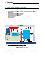
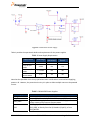
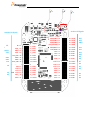
FRDM-KE02Z
User’s Manual
Rev. 0
Freescale Semiconductor Inc.
FRDMKE02ZUM
Table of Contents
1
Overview ................................................................................................................................... 4
2
Reference Documents ............................................................................................................... 4
3
Getting Started.......................................................................................................................... 4
4
FRDM-KE02Z Hardware Overview ............................................................................................. 5
5
FRDM-KE02Z Hardware Description .......................................................................................... 6
5.1
Power Supply .................................................................................................................... 6
5.2
Serial and Debug Adapter (OpenSDA) ................................................................................ 8
5.2.1
5.2.2
Debugging Interface ...................................................................................................................................... 9
Virtual Serial Port .......................................................................................................................................... 9
5.3
KE02Z Microcontroller ....................................................................................................... 9
5.4
Clock Source ...................................................................................................................... 9
5.4.1 Serial Port ........................................................................................................................ 10
5.4.2 Reset ............................................................................................................................... 10
5.4.3 Debug .............................................................................................................................. 10
5.5
Thermistor....................................................................................................................... 10
5.6
Infrared Port.................................................................................................................... 11
5.7
Capacitive Touch Slider.................................................................................................... 11
5.8
3-axis Accelerometer ....................................................................................................... 12
5.9
RGB LED .......................................................................................................................... 13
5.10
Input/Output Headers ..................................................................................................... 13
5.11
Arduino Compatibility...................................................................................................... 14
List of Figures
Figure 1. FRDM-KE02Z Block Diagram ............................................................................................... 5
Figure 2. FRDM-KE02Z Power Supply ................................................................................................ 7
Figure 3. OpenSDA Block Diagram .................................................................................................... 9
Figure 4. SWD debug connector to KE02Z ......................................................................................... 9
Figure 5. Thermistor connection ..................................................................................................... 11
Figure 6. Infrared connection .......................................................................................................... 11
Figure 7. Touch Slider connection ................................................................................................... 12
Figure 8. Accelerometer connection ............................................................................................... 12
Figure 9. RGB LED connection ......................................................................................................... 13
Figure 10. I/O headers .................................................................................................................... 14
FRDMKE02ZUM
FRDM-KE02Z User Manual
Page 2 of 14
Revision History
Revision
0
FRDMKE02ZUM
Date
4/17/2014
Changes
Initial version
FRDM-KE02Z User Manual
Page 3 of 14
1 Overview
The Freescale Freedom development platform is an evaluation and development tool ideal for rapid
prototyping of microcontroller-based applications. The hardware design is form-factor compatible
with popular third-party hardware designed to work with Arduino™ and Arduino-compatible
boards.
The Freescale KE02Z freedom board (FRDM-KE02Z) is a simple, yet sophisticated design featuring a
Kinetis E Series microcontroller KE02Z64VQH2, the industry’s first microcontroller built on the
ARM® Cortex™-M0+ core with 0.18um process.
The Kinetis E series is the most scalable portfolio of low-power, high-robustness, mixed signal 32-bit
ARM Cortex-M0+ MCUs running up to 20MHz in the industry based on .18um process. It supports
power supply voltage range from 2.7V to 5.5V, ambient operating temperature ranges from -40C to
105C and includes up to 64KB flash.
The FRDM-KE02Z includes the Freescale open standard embedded serial and debug adapter known
as OpenSDA. This circuit offers the user several options for serial communications, flash
programming and run-control debugging.
There are also many software development tool options available to the user. Choices include
CodeWarrior for Microcontrollers, IAR Embedded Workbench, Keil MDK featuring the µVision IDE,
Red Suite from Code Red Technologies, Atollic TrueSTUDIO, Rowley Crossworks, and more.
All of these features combine to give the user the freedoms needed to rapidly prototype many
embedded designs: a powerful microcontroller built on a very low-power core and SoC platform,
easy-access to I/O with a large ecosystem of compatible hardware, a flexible programming and
debug interface, and a large ecosystem of software development environments. Freedom!
2 Reference Documents
OpenSDA User’s Guide
KE02 Sub-Family Reference Manual
Arduino Overview
Arduino Uno
-
A guide for users of the OpenSDA embedded circuit.
A reference manual for KE02 sub-family devices
A guide of Arduion platform
A guide of Arduion Uno revision
3 Getting Started
Refer to the FRDM-KE02Z Quick Start Package for step-by-step instructions for getting started with
the FRDM-KE02Z. See the Jump Start Your Design section on http://www.freescale.com/FRDMKE02Z for the Quick Start Package and software lab guides.
FRDMKE02ZUM
FRDM-KE02Z User Manual
Page 4 of 14
4 FRDM-KE02Z Hardware Overview
The FRDM-KE02Z hardware is a Freescale Freedom development platform
platform microcontroller board
assembled with the following features:
• Kinetis E Series KE02
2 family MCU in an 64 QFP package (14x14 document number:
98ASB42844B)
• On-board
board serial and debug adapter (OpenSDA)
• I/O headers for easy access to MCU I/O pins
• Freescale inertial sensor, MMA8451Q
• Capacitive touch slider
• Reset pushbutton
• RGB LED
• infrared communication
• 1 thermistor
• Motor control header for simple BLDC motor control on APMOTOR56F8000E
Figure 1 shows a block
lock diagram of the FRDM
FRDM-KE02Z board.
Figure 1. FRDM-KE02Z Block Diagram
The FRDM-KE02Z features two microcontrollers (MCUs): the target MCU and a serial and debug
adapter (OpenSDA) MCU. The target MCU is a Kinetis E Series MA64 family device, the
KE02Z64VQH2.. The OpenSDA MCU is a Kinetis
Ki tis K Series K20 family device, the K20DX128VFM5.
Features of the KE02Z64 target MCU include:
•
•
•
•
•
•
•
•
•
32-bit ARM Cortex-M0+ core
- up to 20 MHz operation
- Single-cycle fast I/O access port
Memories
- 64 KB flash and 256B D-flash as EEPROM
- 4 KB SRAM
System integration
- Power management and mode controllers
- Low-leakage wakeup unit
- Bit manipulation engine (BME) for read-modify-write peripheral operations
Clocks
- Clock generation module with FLL for system and CPU clock generation
- 32 kHz internal reference clock
- System oscillator supporting external crystal or resonator
- Low-power 1kHz RC oscillator for RTC and watchdog
Analog peripherals
- 12-bit SAR ADC
- Tow analog comparators
Communication peripherals
- Two 8-bit Serial Peripheral Interfaces (SPI)
- one I2C modules
- Three UART modules
Timers
- One 6-channel FlexTimer module
- Two 2-channel Timer/PWM modules
- 2-channel Periodic Interrupt Timer (PIT)
- Real time clock (RTC)
- System tick timer
- One watchdog module
Security
- One CRC
Human-Machine Interfaces (HMI)
- General purpose input/output controller
- IRQ
5 FRDM-KE02Z Hardware Description
5.1 Power Supply
The FRDM-KE02Z offers a design with multiple power supply options. It can be powered from the
USB connector, the VIN pin on the I/O header, an off-board 1.71-3.6V supply from the 3.3V pin on
the I/O header or 3.3V from motor control header . The USB and VIN supplies are regulated onboard using a 3.3V linear regulator to produce the main power supply. The other two sources are
not regulated on-board. The following figure shows the schematic drawing for the power supply
inputs and the on-board voltage regulator.
FRDMKE02ZUM
FRDM-KE02Z User Manual
Page 6 of 14
Figure 2. FRDM-KE02Z Power Supply
Table 1 provides the operational details and requirements for the power supplies.
Table 1. Power Supply Requirements
5V
OpenSDA
Operational?
Yes
Regulated onboard?
Yes
4.3-9V
No
Yes
1.71-3.6V
No
No
3.3V
Yes
No
Supply Source
Valid Range
OpenSDA USB (J7)
VIN Pin on I/O
header
3.3V Pin on I/O
header
3.3V Pin on motor
control header
Note that the OpenSDA circuit is only operational when a USB cable is connected and supplying
power to J6. However, the protection circuitry is in place to allow multiple sources to be powered
at once.
Table 2. FRDM-KE02Z Power Supplies
Power Supply Name
P5-9V_VIN
P5V_SDA
P3V3_VREG
P3V3
FRDMKE02ZUM
Description
Power supplied from the VIN pin of the I/O headers (J9 pin 16).
Power supplied from the OpenSDA USB connector (J6).
Regulated 3.3V supply. Sources power to the P3V3 supply rail
through a back drive protection Schottky diode.
Main supply rail for the FRDM-KE02Z. can be sourced from
P3V3_VREG, or directly from the I/O headers (J9 pin 8), or from
P3V3_MOTOR.
FRDM-KE02Z User Manual
Page 7 of 14
P3V3_KE02Z
P3V3_SDA
P5V_USB
KE02Z MCU power supply. Header J3 provides a convenient means
for KE02Z energy consumption measurements.
OpenSDA circuit power supply. Header J4 provides a convenient
means for K20 energy consumption measurements.
Nominal 5V supplied to the I/O headers (J9 pin 10). Sourced from
P5V_SDA supply through a back drive protection Schottky diode.
3.3V supply from motor control header
P3V3_MOTOR
Notes:
1) J3 and J4 are not populated by default on the production version. The
two pins of these headers are shorted together by 0 ohm resistor R11 and
R26 on the PCB. To measure the energy consumption of either the
KE02Z64 or the OpenSDA MCU, the 0 ohm resistor between these pins
must first be cut. A current probe or a shunt resistor and voltage meter
can then be applied to measure the energy consumption on these rails.
When the MCU current measurement is done with no further need, this 0
ohm resistor can be soldered on again.
2) To better get ADC accuracy on KE02Z64, it is recommended that a 0 ohm
resistor R13 be soldered on and ensure there is no power supply from
P3V3_MOTOR and P3V3 sourced from I/O headers.
5.2 Serial and Debug Adapter (OpenSDA)
OpenSDA is an open-standard serial and debug adapter. It bridges serial and debug
communications between a USB host and an embedded target processor as shown in Figure 3. The
hardware circuit is based on a Freescale Kinetis K20 family microcontroller (MCU) with 128 KB of
embedded flash and an integrated USB controller. OpenSDA features a mass storage device (MSD)
bootloader, which provides a quick and easy mechanism for loading different OpenSDA
Applications such as flash programmers, run-control debug interfaces, serial-to-USB converters, and
more. Two or more OpenSDA applications can run simultaneously. For example, run-control debug
application and serial-to-USB converter runs in parallel to provide a virtual COM communication
interface while allowing code debugging via OpenSDA with just single USB connection. These two
applications are provided in a single code package.
Refer to the OpenSDA User’s Guide for more details.
FRDMKE02ZUM
FRDM-KE02Z User Manual
Page 8 of 14
Figure 3. OpenSDA Block Diagram
OpenSDA is managed by a Kinetis K20 MCU built on the ARM® Cortex™-M4 core. The OpenSDA
circuit includes a status LED (D4) and a RESET pushbutton (SW1). The pushbutton asserts the Reset
signal to the KE02Z target MCU. It can also be used to place the OpenSDA circuit into Bootloader
mode by holding down the RESET pushbutton while plugging the USB cable to USB connector J6.
Once the OpenSDA enters bootloader mode, other OpenSDA applications such as debug app can be
programmed.
SPI and GPIO signals provide an interface to the SWD debug port of the KE02Z. Additionally, signal
connections are available to implement a UART serial channel. The OpenSDA circuit receives power
when the USB connector J6 is plugged into a USB host.
5.2.1 Debugging Interface
Signals with SPI and GPIO capability are used to connect directly to the SWD of the KE02Z. These
signals are also brought out to a standard 10-pin (0.05”) Cortex Debug connector (J7) as shown in
Figure 4. It is possible to isolate the KE02Z MCU from the OpenSDA circuit and use J7 to connect to
an off-board MCU. To accomplish this, cut the 0 ohm resistor R58. This will disconnect the
SWD_CLK pin to the KE02Z so that it will not interfere with the communications to an off-board
MCU connected to J7.
Figure 4. SWD debug connector to KE02Z
5.2.2 Virtual Serial Port
A serial port connection is available between the OpenSDA MCU and UART1 pin PTC7 (TXD1) and
PTC6 (RXD1) of KE02Z. Several of the default OpenSDA Applications provided by Freescale,
including the MSD Flash Programmer and the P&E Debug Application, provide a USB
Communications Device Class (CDC) interface that bridges serial communications between the USB
host and this serial interface on the KE02Z.
5.3 KE02Z Microcontroller
5.4 Clock Source
The Kinetis KE02 microcontrollers feature an on-chip oscillator compatible with two ranges of input
crystal or resonator frequencies: 32 kHz (low frequency mode), 4-20 MHz (high frequency mode).
The KE02Z64 on the FRDM-KE02Z is clocked from a 10 MHz crystal.
FRDMKE02ZUM
FRDM-KE02Z User Manual
Page 9 of 14
5.4.1 Serial Port
The serial port interface signals used with OpenSDA are UART1 pin PTC7 (TXD1) and PTC6 (RXD1).
These signals are also connected to I/O header J1.
5.4.2 Reset
The PTA5/RESET signal on the KE02Z is connected externally to a pushbutton, SW1. The reset
button can be used to force an external reset event in the target MCU. The reset button can also
be used to force the OpenSDA circuit into bootloader mode when plugging the USB cable to J6.
Please refer to the Serial and Debug Adapter (OpenSDA) section for more details.
5.4.3 Debug
The sole debug interface on all Kinetis E Series devices is a Serial Wire Debug (SWD) port. The
primary controller of this interface on the FRDM-KE02Z is the onboard OpenSDA circuit. However,
a 2x5-pin (0.05”) Cortex Debug connector, J7, provides access to the SWD signals for the KE02Z
MCU. The following table shows SWD connector signals description for KE02Z:
Table 3. ARM JTAG/SWD mini Connector Description
Pin
1
Function
VTref
2
3
4
5
6
7
8
9
10
SWDIO/TMS
GND
SWDCLK/TCK
GND
SWO/TDO
NC
TDI
NC
RESET
Connection to KE02Z
3.3V system power supply
(V_BRD)
PTA4/SWD_DIO
GND
PTC4/SWD_CLK
GND
NC
NC
NC
NC
PTA5/RESET
5.5 Thermistor
One thermistor (RT1) is connected to two ADC inputs (PTF4/ADP12, PTF5/ADP13) of KE02Z for
evaluating the ADC module.
FRDMKE02ZUM
FRDM-KE02Z User Manual
Page 10 of 14
Figure 5. Thermistor connection
5.6 Infrared Port
One infrared Rx port and one tx port as shown in Figure 6 are connected to ACMP0 input pin
(ACMP0_IN1) and SCI0 TXD0 pin of KE02Z to demonstrate the capability of SCI0 modulated by
Flextimer for generating infrared signals and use ACMP0 as a filter to receive the SCI data via
infrared signal.
Figure 6. Infrared connection
5.7 Capacitive Touch Slider
Two GPIO pins functioning as Touch Sense Input (TSI) signals, are connected to capacitive
electrodes configured as a touch slider as shown in Figure 7 below:
FRDMKE02ZUM
FRDM-KE02Z User Manual
Page 11 of 14
Figure 7. Touch Slider connection
5.8 3-axis Accelerometer
A Freescale MMA8451Q low-power, three-axis accelerometer is interfaced through an I2C bus and
two GPIO signals as shown in Table 4 below. By default, the I2C address is 0x1D (SA0 pulled high).
Table 4. Accelerometer Signal Connections
MMA8451Q
SCL
SDA
INT1
INT2
KE02Z
PTA3
PTA2
PTD4
PTD3
Figure 8. Accelerometer connection
FRDMKE02ZUM
FRDM-KE02Z User Manual
Page 12 of 14
5.9 RGB LED
Three PWM-capable KE02Z signals are connected to a red, green, blue LED. The signal connections
are shown in Table 5 below.
Table 5. RGB LED Signal Connections
RGB LED
Red Cathode
Green Cathode
Blue Cathode
KE02Z
PTH1/FTM2CH1
PTH2/FTM1CH0
PTE7/FTM1CH1
Figure 9. RGB LED connection
5.10 Input/Output Headers
The KE02Z64 microcontroller is packaged in an 64-pin QFP. Some pins are utilized in on-board
circuitry, but many are directly connected to one of four I/O headers (J1, J2, J9 and J10). J1 and J2
also function as motor control headers to provide access to a motor control board such as simple
BLDC motor driving board APMOTOR56F8000E.
FRDMKE02ZUM
FRDM-KE02Z User Manual
Page 13 of 14
Arduino R3 Signals
Arduino R3 Signals
NC
IOREF
RESET
3.3V
5V
GND
GND
VIN
A0
A1
A2
A3
A4
A5
NC - 2
P3V3_-
-4
1 -PTE0
RESET - 6
5 -PTE2
P3V3 - 8
7 -PTE3
9 -PTD2
P5V_USB - 10
GND - 12
GND - 14
P5-9V_VIN-
- 16
3 -PTE1
11 -PTF1
13 -PTF0
15 -PTG3
PTB3/ANB2-
- 19
20 -PTA3
PTA7/ANB1-
- 17
PTA6/ANB0-
- 15
P3V3_MOTOR-
- 13
18 -PTA2
PTF6/ANA1-
- 11
14 -GND
12 -PTB2
PTF7/ANA0 - 9
10 -PTB4
PTF2 - 7
Figure 10. I/O headers
5.11 Arduino Compatibility
16 -AREF
PTF3 - 5
PTC1 - 3
PTB2 - 1
8 -PTB3
6 -PTB5
4 -PTH0
2 -PTA0
PTE5 - 15
16 -PTA7
PTE6 - 13
14 -PTB4
The I/OPTF7-
headers
boards
- 2 on the FRDM-KE02Z
1 -PTG1 are arranged to allow compatibility
PTC5 - 11 with peripheral
12 -
PTD1
(know PTC0
as shields)
that
connect
to
Arduino
and
Arduino-compatible
microcontroller
boards.
The
PTE4 - 9
-4
3 -PTG2
10 -PTA1
pins onPTC1
the -
headers
share the
same
on the
5-
PTG0mechanical spacing and placement
PTD6 - 7as the I/O headers
8 -PTD0
6
Arduino
Uno
Revision
3
board
design.
See
Figure
10
for
compatible
signals.
7 -PTC4
PTC2 - 8
-
PTC3 - 10
PTF6 - 12
9 -PTH7
11 -PTH6
PTD7 - 5
6 -PTD5
PTC6 - 3
PTC7 - 1
4 -PTB1
2 -PTB0
D15
D14
AREF
GND
D13
D12
D11
D10
D9
D8
D7
D6
D5
D4
D3
D2
D1
D0