1
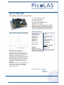
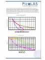
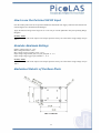
User Manual Rev. 1410 LDP-AV D06-N20 PicoLAS GmbH Company for Innovative Power Electronics and Laser Technology Kaiserstrasse 100 52134 Herzogenrath Distribution: Table of Contents LDP-AV D06-N20 ...................................................................................................................................3 How to get started.....................................................................................................................................4 How to connect the LDP-AV ...................................................................................................................5 Laserdiode Connection.............................................................................................................................6 Internal Structure of the LDP-AV ............................................................................................................7 Dos and Don´ts.........................................................................................................................................8 Operating Range.......................................................................................................................................8 Trigger Delay .........................................................................................................................................10 How to use the Internal HV-DC-Supply ................................................................................................10 How to use the External HV-DC Input ..................................................................................................11 Absolute Maximum Ratings...................................................................................................................11 Mechanical Details of the Base-Plate .....................................................................................................11 2 LDP-AV D06-N20 Rev. 12.12 LDP-AV D06-N20 Very short pulse driver module 4 .. 30 A output current 2 ns pulse durat ion < 900 ps rise time Very compact OEM-module Single +15 V supply Rep. rates from single shot to 2 MHz Current monitor and isolat ed monitor Applications: LIDAR, Measurements, Ignition, Rangefinding, Biochemistry, ... Technical Data:* Output current Max. Output voltage -Int. High Voltage Rise time Typ. trigger delay Pulse duration Trigger range Trigger input Trigger output Current monitor Supply voltage Figure: Optical output Product Description: Dimensions Weight Operating temperature 4 .. 30 A 120 V 15 .. 120 V, 0.1 A, 15 W Typ. 800 ps, max. 900 ps Typ. 36 ns, max. 40 ns 2.0 ns single-shot to 2 MHz * * 5 V into 50 Ω via SMC-jack galvanically sep. Rogow ski-coil 20 A/V into 50 Ω +15 V, 1 A Optional: 0 .. 120 V, 15W (External high-voltage) 65 x 44 x 20 mm 76 g -20 to + 55 ° C * M easured into a short instead of laser diode. Technical data is preliminary and subject to change w ithout further notice. * * Refer to manual for detailed information. The LDP-AV-Series provides a small and inexpensive source for fixed picosecond and nano-second pulses. The LDP-AV D06-N20 is designed for a pulse duration of 2 ns. It is intended to be used as a laser diode driver. The diodes can be mounted directly onto the LDP-AV, eliminating the need for strip lines. The LDP-AV is powered by a single 15V DCsupply, a 120V high voltage DC source is integrated. Additionally the LDP-AV can be upgraded with the PLCS-21 controller to enable USB2.0 communication with a PC or the external operating unit PLB-21. Optional Accesories: 3 PLCS-21 PLB-21 LDP-V-BOB LDP-V-KIT How to get started Step # What to do 1 Unpack your Device 2 Make a short at the output e.g. with a thin copper foil. 3 Set the High voltage to the lowest value (turn Poti fully counterclockwise) 4 Connect a Pulse source to the selected triggering Input Check e.g. 100 ns, Reprate 1 kHz, 5 V TTL 50 Ohm. Note: The applied duty cycle should be less than d=0.2. See section “Triggering input” for more details. 5 Connect your Scope Select 50 Ohm termination, trigger on falling edge, 200 mV/div. 6 Apply the supply voltage Security Advise: Do not touch any leads of the output or the output capacitors as they are connected to a high voltage of up to 120 V Plug in the delivered plug or adjust your Supply to 15.0 V Note: Some supplies have a voltage overshoot during turn on/turn off. This may damage the device. 7 Adjust the value of the desired pulse current by adjusting the level of the HV with the poti. 8 Disconnect the supply, remove the short at the output and assemble the Laser Diode (Polarity!) 9 Reconnect the Supply and check the optical output of your Laser Diode. Note: The actual current is always some percent lower but never higher than the value of step 7. Adjust the current to the desired value. 4 How to connect the LDP-AV Solder-junction to activate the internal HV-supply Rogowski-Coil (No terminal mounted) Poti to adjust value of HV-DC Pin 10 Pinheader Pin 2 Laser-DiodeConnection Trigger-Input SMC Current-Monitor SMC Connections via Pinheader Pin 1 Name Description Ground return GND 2 HV+ External high-voltage supply Input (0..120 V) for connecting an alternative HVDC supply. See section “How to use the external HV-DC Input” for details. 3 GND Ground return 4 +15 V Supply voltage, connect to a power supply. 5 Disable_Poti Disables the internal HV-setpoint poti when set high. 6 Pulse_In Trigger input into 50 Ohm 7 Disable Disables the Driver when set high. 8 U-Monitor High-voltage monitor output (scale: 40 mV/V) for supervising the actual high voltage 9 NTC Internal 10 kOhm NTC versus GND for temperature monitoring (B-value: 3620) 10 Ext_HV_Setpoint External HV setpoint input (scale: 25 V/V) allows control over the internal HVDC source Trigger Input: The trigger input requires a signal of 5 V and is terminated with 50 Ohm. The minimum input signal pulse width is 10 ns. For more details see below. Current Monitor Output: The current monitor output has a scale of 20 A/V with a negative signal output. It has a source impedance of 50 Ohm and must be terminated with 50 Ohm to achieve the correct scale. Laser Diode Connection: The Laser Diode can either be connected via the mounting holes on the top side of the driver (inner hole: Anode, outer hole: Cathode) or at the rectangular pads on top (Anode) and bottom (Cathode). Security Advise: Do not touch any leads of the output or the output capacitors as they are connected to a high voltage of up to 120 V. Laserdiode Connection Many elements and parasitic “stray” components may affect the performance of the LDP-AV. The stray inductance of the load connected to the driver is very important. “Load” means not only the diode itself but also the packaging (bondwires!) and leads between the driver and the diode. However, PicoLAS has no influence on these parts. Thus, all measurements have been performed into a short instead of a laser diode. Refer to the PicoLAS Appnotes # 2 (Impedance of Diodes) and # 3 (LD-Connections) to get more information about parasitic elements and their effect on the pulse shape. 6 Internal Structure of the LDP-AV Pin 2: + HV Pin 8: U-Monitor +HV-Adjust-Poti 15 V Pin 4: +15 V 15 .. 120 V Rx Pin 5: Disable Poti Cx Pin 10: Ext. HV setpoint CS Pin 7: Disable Pin 1,3: GND Pin 6: Trigger T1 Trigger SMC Pin 9: NTC 50 R Driver Rogowski-Coil 10K Current-Monitor 50 R Rogowski-Coil The LDP-AV generates the pulses by a simple but efficient principle. First, the capacitors Cx are charged over Rx, whether through the internal HV-DC-supply or an external high voltage source. When a pulse is applied at the trigger input, the high speed MOSFET T1 closes and the current flows from the capacitor through the laser diode, MOSFET, Coil and resistors. Cx generates an oscillating circuit with the coil and the resistors. Due to the constant values of these elements the oscillating frequency and thereby the pulse width is kept constant. The output pulse is not affected by the length of the trigger input pulse. The generated current depends on the applied high voltage, the laser diode compliance voltage and its differential resistance. The time that T1 is open is not relevant for the pulse length. Certainly the input pulse of the trigger input has to be minimal 10 ns. For longer input pulses the output pulse form is not changing but the stress of the driver increases. So the duty cycle of the input pulse is limited to d= 0.2. Applications with very high frequencies have special specifications (see chapter “Operating Range” for more details). The following diagram shows the output current (at current monitor, measured with a short at the output) for different high voltages. 7 Output Pulse Diagram: LDP-AV-D06-N20 typ. Pulse output (1.25ns/div, 5 A/div) Traces corresponding to 40, 60, 80, 100 and 120 V HV-precharge The laser diode current is measured with current sensing resistors (current monitor output) and with the galvanically isolated rogowski coil. Disable- and trigger-input provide full control of the driver’s pulsing capability to the user. The required DC high-voltage can either be applied through an external voltage source or it can be generated with the integrated HV-DC-supply. The internal supply is controlled by the HV setpoint poti or, when the Disable_Poti (Pin 5) pin is set high, via the Ext_HV_setpoint (Pin 10) pin. A voltage monitor (Pin 8) provides feedback of the high dc voltage. The antiparallel Diode prevents the laser diode from reverse currents; a 10kR NTC provides the possibility to monitor the pulser temperature. An over temperature protection is NOT integrated on the driver. Dos and Don´ts • • • • • • Do not exceed specified parameters. Do not connect voltages with a reverse polarity to the device Never connect more than 18.0 V to the power terminals of the device. Beware: Some Lab-Power Supplies cause excessive ringing during powering on and off. These may damage the unit! Pay attention to proper cooling! Attention: Do not touch the unit during operation: High voltage! Operating Range 8 Due to the structure of the driver the maximum duty cycle of the trigger input (the driver output is not affected!) must be lower than d=0.2. During a “HIGH” signal at this input the main switching MOSFET is switched on and the high voltage is dropped over the resistor Rx. In fact the stress of this resistor is quite big. When the MOSFET turns off the capacitor Cx is charged over the same resistor and stresses it additionally. Especially for high frequencies (f > 500 kHz) this is the main part of the stress of Rx. If using the driver in a high frequent application, the high voltage and the duty cycle have to be adjusted. The following tables show the maximum parameters for these values. maximum pulse width of trigger input 600 maximum pulse width of trigger input in ns 500 400 300 200 100 0 0,1 0,2 0,3 0,4 0,5 0,6 0,7 0,8 0,9 1 1,1 1,2 1,3 1,4 1,5 1,6 1,7 1,8 1,9 2 2,1 frequency in MHz U=80V U=100V U=120V maximum duty cycle of 0.2 maximum high voltage 130 120 110 high voltage in V 100 90 80 70 60 50 40 0,1 0,3 0,5 0,7 0,9 1,1 1,3 frequency in Hz 1µs 100ns 9 10ns 1,5 1,7 1,9 2,1 Trigger Delay The delay between the triggering signal and the load-current is very low around 35 ns and very constant. The pulse-to-pulse jitter is very stable below 50 ps if supply voltage and temperature are kept constant. The output pulse is not affected by the length of the trigger input pulse. How to use the Internal HV-DC-Supply The LDP-AV series provides a high power (up to 20 W / 2 A / 120 V) internal high voltage supply. To adjust the laser diode current to the desired value follow the steps below. Notice: Make sure that the solder junction is done to activate the HV-DC-Supply and the supply voltage is 15 V. 1. 2. 3. 4. 5. Turn the poti fully counterclockwise Apply the 15 V supply voltage Start Pulses Measure the diode current Adjust the level of the high voltage supply (hence the level of the current) by turning the poti clockwise Security Advise: Do not touch any leads of the output or the output capacitors as they are connected to a high voltage of up to 120 V. 10 How to use the External HV-DC Input First the solder junction has to be opened to disable the internal HV-DC supply. Otherwise the external and internal supplies are shorted and both damaged. Apply the desired voltage in the range of 0 V to 120 V at pin 2 of the pinheader. Obey the Operating Range Diagram! Security Advise: Do not touch any leads of the output or the output capacitors as they are connected to a high voltage of up to 120 V. Absolute Maximum Ratings Supply voltage range: 10 .. 18 V Max. voltage at HV Pin: 120 V Max. output current U-monitor, NTC: 1 mA Input voltage range Disable_Poti, Ext_HV_Setpoint: 0 .. 5 V Input voltage range trigger input, Disable: 0 .. 15 V Security Advise: Do not touch any leads of the output or the output capacitors as they are connected to a high voltage of up to 120 V. Mechanical Details of the Base-Plate LDP-AV D06-N01 11