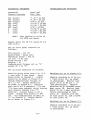
1
0852-0100
MODEL
1 March 1978
8~1-D
LOGIC ANALYZER
OPERATING AND SERVICE MANUAL
•
(408) 988-6800 •
TWX (910) 338-0509 •
OPERATING AND SERVICE MANUAL
MODEL 85l-D
Table of Contents
Page
Section
I
II
III
General Information
1.1
Certification
1
1.2
Warranty
1
1.3
Instrument Description
1
1.4
Specifications
2
Installation
2.1
Introduction
5
2.2
Unpacking and Inspection
5
2.3
Storage and Shipment
5
2.4
Power Connections
5
2.5
Preparation for Use
6
2.6
Initial Warm-Up
6
Principles of Operation
7
3.1
Basic Functional Description
3.2
Recording Considerations
10
3.3
Outputs and Control Inputs
12
3.4
Operational Functions
13
Page
Section
IV
V
VI
Operation
4.1
Introduction
16
4.2
Front Panel Controls and
Connectors
16
4.3
Rear Panel Controls and
Connec.tors
23
4.4
Set-Up Procedure
25
4.5
Operating Procedure
28
Output Interface
5.1
Introduction
30
5.2
Digital Output
30
Calibration Procedure
6.1
Calibration of Display Output
33
6.1
Recalibration of the Internal
Circuits
33
6.3
Required Test Equipment
33
6.4
Power Supply Adjustment
34
6.5
Channel 1-4 and 5-8 Threshold
Adjustments
34
6.6
Input Offset Adjustments
35
6.7
Input Capacitance
35
Page
Section
VII
VIII
IX
Technical Description
7.1
General Description
37
7.2
Detailed Description
42
7.3
Control Board
42
7.4
Main Board
49
7.5
Power Supply
54
Maintenance Procedures
8.1
Maintenance
60
8.2
Required Test Equipment
60
8.3
Diagnostic and Troubleshooting
Procedures
61
8.4
Disassembly Procedure
71
Schematics and Assembly Drawin9:s
9.1
Introduction
74
9.2
Logic Symbols and Reference
Designators
74
9.3
List of Drawings
75
SECTION I
GENERAL INFORMATION
1.1
Certification
Biomation Corporation certifies that this instrument
was thoroughly tested and inspected and found to meet its
published specifications when it was shipped from the factory.
1.2
Warranty
All Biomation products are warranted against defects
in materials and workmanship. This warranty applies for one
year from the date of delivery, or, in the case of certain
major components listed in the operating manual, for the
specified period. We will repair or replace products that
prove to be defective during the warranty period. No other
warranty is expressed or implied. We are not liable for
consequential damages. For complete warranty statement, see
end of manual.
1.3
Instrument Description
The 851-0 Logic Analyzer is a new instrumentation tool
for the design and repair of digital logic circuits. Complex
logic timing relationships can be conveniently recorded, displayed, and analyzed. Eight channels of digital information
can be recorded and monitored at rates up to 50 MHz.
The Biomation Model 851-0 is designed specifically for
analysis of digital logic circuits and signals. The unit can
be used on both synchronous and asynchronous signals and can
detect random logic pulses as narrow as 5 nsec with· the use
of the "LATCH" input feature.
The Model 851-D Logic Analyzer provides the ability to
measure up to eight digital signals against a preset threshold,
update the detectors with an internal or external clock, and
store 512 such simultaneous decisions for each input signal.
Threshold settings are independently selectable for Channels
1-4 and 5-8. This information is then presented for display
-1-
on an oscilloscope in an eight trace timing-diagram presentation. Thus, the user can capture unique combinations
of digital events for concise and rapid analysis.
Specifications for the Model 851-D are given in the
following paragraphs.
1.4
Specifications
SIGNAL INPUTS
Number.
8.
Impedance.
1 MQjlO pF.
Inputs greater than +12 V clamped
tot12 V through 10 kn.
Two Threshold Controls. Channels 1-4 independent from
Channels 5-8. Selectable TTL, ECL, MST,
+0.25, -0.25, and +0.20 V. Continuously variable
+2.4 V. Selectable for Xl or XIO probes.
Max Overload Voltage.
Input Modes.
+50 V continuous, +100 V transient.
Selectable; SAMPLE or LATCH.
Sample Mode.
Unit stores the detected logic level
present at each positive clock transition
simultaneously on all input channels. Maximum channel-to-channel time skew of this clocked
data is <1 nsec. Minimum pulse width always
detected and recorded is one clock plus 2 nsec
with 250 mV or more threshold overdrive.
Latch Mode.
Threshold detector latches in state opposite
that stored at previous clock transition in
the event that multiple transitions of the
threshold occur prior to the next clock transition.
Minimum Pulse width to Latch.
5 nsec with typically 250 mV
overdrive beyond actual threshold.
CLOCK
Internal.
Selectable 0.02, 0.05, 0.1, 0.2, 0.5, 1, 2, 5,
10, 20, microseconds or milliseconds clock
intervals.
-2-
External.
Via front panel BNC connector, continuous rates
from 50 MHz to DC. External clock signal threshold
set on threshold selection for Channels 5-8. Positive or Negative edge may be selected. 1 MQ input.
Fixed delay between input data signals and external
clock input at the threshold detectors is typically
13 nsec.
TRIGGER
Source.
Selectable; internal, external, or manual.
Internal.
Combinational triggering; Selectable "1, Don't Care,
or 0" for all eight channels. May be triggered
when selected combination appears at inputs or
triggered when combination disappears from the
eight inputs.
External.
Via rear panel BNC connector, ECL level or I/O
connector, TTL level.
Static Delay. With Delayed Record mode selected and the
settable Trigger Delay at zero, the fixed delay
between the detected trigger and the first stored
data in the memory is 4 sample intervals.
Jitter.
Data from repetitive record cycles with respect to
the input signals will exhibit 1 clock interval
maximum time jitter.
MEMORY
Size.
8 X 512 bits.
Record Mode.
Selectable Pretrigger and Delayed record modes.
Pretrigger.
Start via front panel momentary ARM switch, auto
start selection or via rear panel BNC, ECL level or
via TTL level into I/O connector.
0-500 pretrigger
samples. Stop via trigger detection and after selectable delay, or via front panel momentary switch.
Delayed.
Selectable trigger delay via front panel decade
switches to 9999 clock periods, in single clock
increments. Record starts after trigger delay
has elapsed and stops when 512 bits per channel
have been recorded.
DISPLAY OUTPUTS
X Output.
Repetitive 1 V p-p ramp waveform 2 msec period.
Y Output.
Repetitive 1 msec stair step ramp, each step
equally spacea ln amplitude. Data for each
channel modulates each respective step level.
-3-
Xl expansion outputs SOO bits per line.
range nominally 0 to +1 V.
z
Full
Output.
Nominal zero to +S V pulse.
synchronized with X ramp.
1 msec wide
Z Output.
Nominal +S V to zero pulse.
synchronized with X ramp.
1 msec wide
Cursor.
Movable display cursor.
Expansion.
XS, XIO, X20 full expansion or mixed expansion.
Mixed expansion Xl to left of movable cursor and
XS, XIO, or X20 expand to right of cursor.
DIGITAL INTERFACE
Data.
Output, 8 bits parallel, TTL levels positive true,
word serial asynchronous data transfer under control of Flag and Command signals.
Rates 30 kHz
down to DC.
Flag.
Output of positive TTL transition indicates data
word on output lines can be read. Minimum pulse
width 2 llsec.
Command.
Input of negative TTL transition requests next
data word. Minimum pulse 3 llsec.
Output Request.
Input of TTL low or ground stops the display
and initiates the digital data output.
Internal Clock Input/Output~
Used for connecting several
8S1-D units together for synchronous recording,
ECL level.
Internal Clock Input/Output. Used for connecting several
8S1-D units together for simultaneous triggering,
ECL level.
Internal Arm Input/Output. Used for connecting several 8S1-D
units together for synchronous arming, ECL level.
TTL remote ARM also available.
MISCELLANEOUS
Operating Temperature Range:
Power:
Size:
Weight:
O-SOoC.
lIS V/230 V RMS, 50-60 Hz.
Height:
S.2 in. (13.2 cm). Width:
12.7S in.
(32.4 cm). Depth:
19.0 in.
( 4 8 • 3 cm).
Approximately 2S Ibs.
-4-
(11. 3 kg).
SECTION II
INSTALLATION
2.1
Introduction
This section contains information on unpacking,
inspection, repacking, storage, and installation of the
Model 851-0.
2.2
Unpacking and Inspection
Inspect instrument for shipping damage as soon as it is
unpacked. Check for broken knobs and connectors; inspect
cabinet and panel surfaces for dents and scratches. If the
instrument is damaged in any way or fails to operate properly,
notify the carrier immediately. For assistance of any kind,
including help with instruments under warranty, contact your
local Biomation representative or Biomation in Santa Clara,
California, U.S.A.
2.3
Storage and Shipment
To protect valuable electronic equipment during storage
or shipment, always use the best packaging methods available.
Contract packaging companies in many cities can provide dependable custom packaging on short notice.
2.4
Power Connection
Line Voltage: The Model 851-0 may be operated from
either 115, or 230 Vac (+10%) power lines. A rear panel
line voltage switch permits quick and safe conversion for
operation from either voltage.
CAUTION:
Power Cable:
Before plugging instrument into AC
power line be sure line voltage
switch is properly positioned.
The Model 851-0 is equipped with a
detachable 3-wire power cable. Proceed as follows for installation:
a)
Connect line-cord plug C3-socket
connector) to AC line jack at
rear of instrument.
-5-
Power Cable (cont'd)
b)
2.5
Connect plug (2-blade with round grounding pin) to 3-wire (grounded) power outlet. Exposed portions of instrument are
grounded through the round pin on the
plug for safety. When only 2-blade outlet is available, use connector adapter,
then connect short wire from side of
adapter to ground.
Preparation for Use
The Model 851-0 is not a "self-contained" instrument in
that it must be interfaced with other types of instrumentation
for the data to be visible or analyzed. The following sections
of this manual cover operation, set ups, and interface requirements.
2.6
Initial Warm-Up
Although the Model 851-0 is a solid state instrument, a
brief warm-up period of approximately 5 min. is required for the
input amplifiers and comparators to reach thermal stabilization.
This warm-up period is recommended for both the Model 851-0 and
its associated output device.
-6-
SECTION III
PRINCIPLES OF OPERATION
3.1
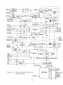
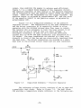
Basic Functional Description
The Model 8Sl-D offers convenient and useful capabilities
for the analysis of digital signals. The unit is an eightchannel solid-state digital recorder, which operates at a maximum record rate of 50 MHz simultaneously for all eight channels.
Figure 3.1 presents a block diagram of the 8Sl-D.
The memory in the 8Sl-D stores a S12-bit record for each
of the eight channels. This memory "snapshot" may be taken in
either of the following record modes: Pre trigger or Delayed
mode.
In the Pretrigger mode the recording process begins
upon activation of ARM switch or Remote Arm input. The unit
continuously monitors and records the status of the eight input lines at the selected clock rate. When a trigger event
occurs; recording is terminated (or continued until the selected trigger delay has elapsed). Selection of the delay
determines the position of the "snapshot" before and after
"-'h~
,,-,...';
~rr"",...
...................... ':::1':::1 .........
"-'h"
'-v'... -......... .T"""
. ...................
~ .,.~.,...,,"-
n"1.,. .... ,,..::1
JJ=~~:L
.........
..,...,......::1,....
... LL'-' ...... =
"-t.,.,,
......... =
...... ",.." ...... ..::I.; ..... rr
L='-''-'L ............... ':::I
....... ,...,...,..".,...,..
./::"L'-''-'-';;>';;;>
begins at the (delayed) trigger event. This means that the
"snapshot" may be delayed downstream from the trigger event at
a selectable number of sample intervals (0 to 9999). Therefore,
eight points in a digital circuit can be continuously monitored,
waiting for a specific fault or logic event. When the event
occurs, a contiguous record of events before and after (Pretrigger mode) or a delayed recording (Delayed mode) is made
for display and subsequent analysis.
3.11
Input Threshold
The definition of a stored data signal as a binary "1"
or "0" is determined by switch-selected logic threshold levels.
Channels 1-4 are independently selectable from Channels 5-8.
Six standard threshold levels are available on each of these
two switches as well as independent, contiguously variable
controls. Standard threshold selections are TTL, ECL, MST,
+2.0, +2.5 and -2.5. The VAR position controls provide
+2.4 V continuously variable for both the input threshold
level selections. In addition, selection of Xl or XIO probe
input selection provides full threshold sensitivity for XIO
attenuated, higher bandwidth probes.
-7-
INPUT
BUFFER
AMPLIFIERS
CH
1-{>-
CH 2 ---...
CH
~
V
LOGIC
LEVEL
COMPARATORS
THRESHOLD
LEVEL
SELECT
CHS. 1-4
-
...
·..
.
CH 5 --.~
·
V
CH 6
-{>~
CH 7
...
CH 8
.~
--
V
-
---
---'v 1-
EXT
TRIGG ER
~y}
~
~
CRT
DISPLAY
SIGNALS
...
...
~
-
-
...
·.
...
..
...
..
...
..
..
.....
--...
-..
~
..
-
..
...
-
...
~
-
~
V
PROBE
CaMP TEST ~
EXT
CLOCK
~
~Z.)
~~
V
~
~X"'"
..
3--[>-
CH 4
..
~
.
OUTPUT
CIRCUITRY
512-BIT
MEMORIES
BUFFERS/
LATCHES
~ THRESHOLD
--·
I-
. ~
I I
V
I
...
LEVEL
SELECT
CHS. 5-8 AND
EXT CLOCK
EXT...
!
I~
---
EXT
TRIGGER
~
..
t>
DIGITAL
OUTPUT
SIGNALS
...
..
~
..
'\~r
..
INT
SAMPLE
INTERVAL
SELECT
Figure 3.1
Sample Mode
3.12
In the "SAMPLE" mode of operation, the input levels
are strobed into the memory as "1" or "0" based on the signal
level with respect to the selected threshold at the time of
the active edge of the clock.
Latch Mode
3.13
The "LATCH" mode of recording permits narrow spikes to
be recorded. Any spike (positive or negative) with sufficient
amplitude and duration causes an input latch to set. This changes
the state of the next bit to be written in memory.
In this way,
narrow spikes or "glitches" occurring at random times between
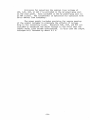
sample clock transitions can be captured.
Typically, a glitch that exceeds the threshold by 250 mV
threshold overdrive can be as short as 5 nsec and still be
detected. See Figure 3.2.
VOLTAGE
OVERDRIVE,
mV
800~
:::jI
500
400l
300
Figure 3.2
Relationship between
voltage over threshold
and pulse width of
glitch that can be
typically latched in
the LATCH mode of
operation.
\
200
100
234
5
6
7
8
9
10
PULSE WIDTH, nsec
3.14
Signal Inputs
The eight signal inputs and the clock input all have an
input impedance of 1 MQ, 10 pF.
3.15
Record Rates
The internal clock interval is switch selectable from
20 msec to 0.02 ~sec, in a 1-2-5 sequence. The clock of the
device or system under test may be input via the front panel
to effect synchronous recording, a distinct advantage when
-9-
synchronous logic is being examined. The external clock logic
threshold is set by the Channel 5-8 threshold selector switch.
Falling or rising clocking edge is also selectable.
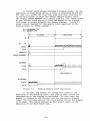
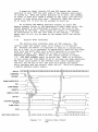
3.16
Delayed Record Mode
,
A Delayed record sequence is started by the Trigger
ftlnction and stops after the entire memory has been refreshed.
The trigger function can be derived from a parallel combination
of input signals, true or false from an external source, or
manually. The trigger can also be delayed by as much as 9,999
clock intervals in single clock increments. This mode and the
Pretrigger record mode are illustrated in Figure 3.3.
In the
Delayed mode a static delay of 4 sample intervals exist from
the trigger event until data is stored in the memory of the
85l-D. The Pretrigger mode must be used to observe the trigger
event and the three samples directly following that event.
3.17
Pretrigger Record Mode
The Pretrigger record mode is unique and very useful.
With the Pretrigger mode selected, the unit begins recording
upon receipt of the Arm command, and continuously updates the
memory with new data (destroying the "oldest" data) much like
recording with a tape loop. The amount of trigger delay selected determines the amount of prior-trigger data stored when
recording ceases; e.g., selection of a 250 clock interval
trigger delay will cause the unit to continue recording for
262 clocks after the trigger, and then cease recording, while
retaining 250 words of contiguous prior trigger data.
In this
way, eight points in a digital circuit can be continuously
monitored, waiting for a specific fault or logic event to
trigger the unit. When the trigger occurs and the delay is
counted out, a contiguous record of events (before and after
the trigger) is recorded and displayed.
3.2
Recording Considerations
Because the Model 85l-D can record as a function of either
the internal clock or an external clock, note should be taken of
some basic differences in these two methods.
When the internal clock is used for recording, no particular
phase relationship will exist between this clock and any synchronous
information rate in the signals being recorded. Therefore, a beat
frequency can exist between these two basic rates.
If the 85l-D
internal clock is at least 10 times higher in frequency than the
signal rate, very little effect will be noted in the recorded data.
For high signal rates (with respect to the record clock), a beat
rate effect can be seen by varying widths in the recorded "pulses"
and even periodic "dropped" bits will be observed when these rates
approach the limiting ratio of two to one.
-10-
CON,]~ROLLING
EVENTS
DELAYED TRIGGER
RECORD MODES
DELAYED SWEEP
TRIGGER.
ARM
+
i(5-
I
I
I
I
HOLD
.
l
I
I
I
(
J
PRETRIGGER
I
RECORD
I
I
I
I
•
+
EOS
flRECORD II
I
I
)...
I
I
..I
PRE TRIG
ME:MORY
SELECTION
I
HOLD
t
EOS
Figure 3.3 Model 85l-D Recording Control Functions
--11-
EOS (End of Sweep)
When the synchronous clock used for the generation of
the input signals to the 851-D is used as the record clock in
the 851-D, no phase errors exist and no beat frequencies will
be evident; i.e., the beat note is zero frequency.
In this
case, signals with information rates up to and including 1/2
the clock frequency can be recorded without distortion. This
is called synchronous recording. The fixed delay between input data signals and the external clock input at the threshold
detectors is typically 13 nsec. See Figure 3.4.
EXTERNAL
CLOCK
t
----~jI
ACTIVE
. E.G. 50 MHz
EDGE
I
I
INPUTDATA_I
I
- - . . I 4 nsec
II
I
t=o
I
RECORDED AS A LOGIC 0
I......~--
I
t= 13 nsec I
t= 17 nsec
Figure 3.4
Sample mode timing requirement. When using an external clock,
data may change states anytime up to typically 13 nsec after
the active edge of the clock. Once the logic state change is
made, it must be maintained until 17 nsec after the active
clock edge to be recorded in that state.
Bear in mind that the 851-D is an instrument for the
detection and storage of digital data. As such, the unit only
discriminates between two different levels as defined by the
threshold switches. The data stored and displayed is NOT an
analog representation of the input signals, but a pattern of
"ones" and "zeros" that represent threshold crossings.
3.3
3.31
Outputs and Control Inputs
Display Output
Once Record is terminated, the unit automatically goes
into a display mode where the contents are repetitively output
to a CRT or triggered scope.
-12-
The display presentation is in an eight-trace timing
diagram format. With no horizontal expansion, 500 bits of information per line are displayed, 50 per division.
The 851-D
has a movable display cursor. This cursor may be used to chose
the point of display expansion. Display expansion may be selected in a mixed mode or in full expansion.
In the mixed expansion setting, the display appears as Xl expansion to the left
of the movable cursor and X5, XlO, or X20 selectable to the right
of the cursor. Full expansion provides 100 bits per line in X5;
50 bits per line in XlO, and 25 bits per line in X20 expansion.
3.32
Digital I/O
The digital data in the Model 85l-D i s memory can be
output under the direction of two digital control inputs via
the rear panel, 24-pin digital interface connector. These
inputs are the OUTPUT REQUEST line and the COMMAND line.
Once digital output has been requested the 85l-D loads an
8-bit parallel word on the output buffers, signaling the
receiving device with a FLAG output signal. These 8 bits
are the first bits of each of the,8 input signals.
Successive
words may be strobed onto the output buffers by the COMMAND
input up to a maximum strobe rate of 30 kHz~ All Data outputs
are TTL levels, positive true. Other input control lines, as
well as output status signals, are available at this connector.
See Section V for complete details.
3 .. 33
Multi-Unit Synchronization
Several 85l-D Logic Analyzers may be synchronized for
extended recording length or increased parallel channel capability.This is done by simply interconnecting the Arm,
Trigger, and Time Base I/O BNC connectors on the rear panel
of each unit.
3.4
Operational Functions
The operation of the Model 85l-D is basically concerned
with the signals or events that determine the initiation and
termination of the sampling and recording of the input signals
and events, and their interrelationships in the functional
operation of the unit.
3.41
Sweep and Sweep Time
In the following discussions the terms "sweep" and "sweep
time" are often used. The term "sweep" is used to designate the
succession of samples taken on the input signals during a recording sequence. The term "sweep time" is used to designate the
amount of time required to fill the memory with ~ontiguous samples
of the input signal. When this term is used, it is normally
assumed that the entire sweep was accomplished at a single linear
sample rate.
-13-
3.42
Arm, Trigger, and End of Sweep Function
The Arm, Trigger, and End of Sweep (EOS) functions, together with adjustable delay (associated with the Trigger event) ,
control the sequence of events in the operation of the record
cycle of the Model 85l-D. The effect of each of these functions
or events on the sequence of events is dependent upon the mode of
operation selected for the unit. This interdependence will be
described below.
In all recording modes, an Arm function must precede a
Trigger function. The unit cannot be triggered before it is
armed. The Arm function may be initiated manually via front
panel pushbutton or externally via rear panel input. Once the
unit has been armed, it can accept a trigger.
The Trigger function may also be initiated in the same
manner as the Arm function.
In addition, the unit may detect
a Trigger from anyone channel, or via the coincidence of a
parallel combination of bits as selected on the front panel.
Furthermore, the combinational trigger selection allows the
85l-D to trigger when the selected parallel combination becomes true with the inputs or, when it no longer coincides
with the selections, becomes false.
3.43
Modes of Operation
The operational modes for the record sequence in the
Model 85l-D are determined by the record mode selected. Three
record modes are provided. They are Pretrigger, Delayed Manual,
and Delayed Auto. The Delayed modes are identical in operation
except for derivation of the Arm signal. In the Delayed Auto
mode the Arm signal occurs automatically after a record sweep
and one complete display output sweep.
In the Delayed Manual
the Arm signal must be provided by activation of the front panel
switch or an external signal input to the rear panel. For purposes of further discussion, Delayed Auto and Delayed Manual will
be treated as Delayed Record Mode. See Figure 3.3 for an
illustrative reference.
3.431
Delayed Record Mode
In the Delayed record mode, the record cycle is
initiated by the (delayed) Trigger, and is ended at the End
of Sweep (EOS) , at which time all 512 bits/channel of the
memory have been loaded with new data.
In the Delayed mode,
there exists a four-sample delay between the start of the
record cycle and storage of data in the memory. This means
that the 512 word "snapshot" is taken four clocks downstream
from the (delayed) triggering event. This mode can be used
in various ways depending on the setting of the Trigger delay.
With the delay set to zero, recording begins at the trigger
event and ends 516 clock intervals later. With a delay set
into the Trigger delay selector, recording is held off until
after receipt of the trigger and timing out of the trigger
delay. When the delay has elapsed the recording process
begins, ending again after 516 clock cycles.
-14-
The delayed sweep mode of operation is used in situations
where the only good trigger signal precedes the data to be recorded.
In many cases the delay between the Trigger and the
desired information is greater than the optimum sweep time.
In these cases the signal would not be recorded with sufficient
resolution to be useful. By delaying the initiation of the
sweep with the Trigger delay and sampling the signal at a
faster rate, the information can be recorded with good time
resolution.
3.432
Pre trigger Mode
Pretrigger recording is a unique feature of Biomation
Recorders. Pretrigger recording allows the capture or recording of signals that are not known to be significant for
recording until after the signal has occurred. Another good
use of this mode is in cases where the only good Trigger
available follows the information of interest.
In the Delayed record mode the starting point for
filling the memory with new information is when the Trigger
occurs, or later.
In the Pretrigger record mode of operation
the memory is continuously being updated after the unit has
been Armed, and will discard information (from the "other
end" of the memory) at the same rate. When a trigger event
occurs, the 85l-D saves the selected Pretrigger portion of
memory and continues recording until the remaining portion
is filled with data occurring after the trigger event.
If
the PRE-TRIG memory switches have been set to 100 bits, the
memory will contain 8 X 100 bits of pretrigger and 8 X 412
bits of data recorded after the trigger.
-15-
SECTION IV
OPERATION
4.1
Introduction
This section identifies and describes front panel controls, rear panel connections, and typical operating procedures.
Included are complete descriptions of front panel controls and
their effective ranges, location and proper use of rear panel
connectors, set up procedures prior to using the Model 85l-D,
and step by step operating procedures for various modes of
operation. A thorough understanding of this section is
essential to the successful use of the instrument.
4.2
4.21
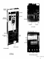
Front Panel Controls and Connectors
Control Clusters
The controls of the Model 85l-D may be divided into
five groups. Each group contains separate controls with related functions.
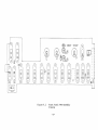
Figure 4.1 is a front panel photograph of
the 85l-D. The five control groups are as follows:
Record Mode and Trigger
Input Mode and Thresholds
Clock
Display
General
4.22
Record Mode and Trigger
(1)
RECORD MODE.
In the PRE-TRIG position, the unit
fills the memory with new data when the front panel MANUAL ARM
switch or remote Arm inputs on the rear panel are activated.
Recording continues, dumping the oldest data off the end of
the memory until the trigger event occurs. At that time the
portion of the memory selected (PRE-TRIG MEMORY (2)) is saved.
The remaining portion of the memory is filled with new data
contiguous to the trigger event.
-16-
I
......
-J
I
Figure 4.1
851-D Front Panel
In the DELAY MAN mode, an Arm initialization alerts
the 851-D that it may accept the next designated trigger
event. When that event occurs, the TRIG DELAY starts. When
the selected trigger delay has elapsed (0 to 9999 clock
intervals), the memory" begins to fill with new data continuing until 512 bits/channel have been recorded.
In the DELAY AUTO mode, the Arm function is activated
by the 851-D internally. Recording is accomplished exactly
as is done in the DELAY MAN mode. Once the 851-D has completed a single display output sweep (requiring 16 msec) , the
unit automatically re-arms itself and will accept the next
designated trigger event. This mode of recording is very
convenient for initial set-up because no manual or external
Arm input signal is required for acceptance of a trigger
event.
(2)
PRE TRIG MEMORY/TRIG DELAY.
In the PRE TRIG
RECORD MODE (1), these convenient digiswitches allocate the
portion of the Model 85l-D's memory that is saved for prior
trigger information. Note that the memory displayed is 500 '
bits/channel long. Setting these switches to 500, therefore,
will place the trigger event at the end of the display memory.
The 499 bits/channel displayed to the left of this trigger
location were recorded prior to the trigger, thereby giving
a look back in time from a trigger event. Attention should
be paid to the amount of time between initialization of the
Arm function and recognition of the Trigger event.
If after
arming the 85l-D only a lOa-clock interval period elapsed
before the trigger event was recognized with the PRE TRIG
MEMORY selection set to 500, the unit would not have had
sufficient time to record all 500 pre trigger samples.
Therefore, 400 samples/channel would be left in the memory
from a previous recording.
The memory is 512 bits/channel long. The first 500
bits/channel are specified to be valid data samples. The
display output sweep consists of only these 500 bits/
channel.
CAUTION:
Setting the PRE-TRIG MEMORY to greater than
500 samples is an illegal mode for the
Model 851-D.
In the DELAY MAN or DELAY AUTO modes, the PRE TRIG
MEMORY/TRIG DELAY designates the amount of delay that elapses
prior to the record start. When a trigger event is recognized
by the Model 85l-D, the beginning of the record cycle may be
postponed from a to 9999 clock intervals. The inherent static
causes the stored data to lag this delay setting by 4 sample
intervals.
-18-
(3) MANUAL ARM. Pressing this momentary switch starts
the unit recording when the RECORD MODE switch (1) is set to
PRE TRIG. In DELAY MAN mode it alerts the 85l-D to accept the
next trigger event. When recording in the pretrigger mode, the
entire memory may be set to all "zeros" (low) by holding the Arm
switch down for a minimum of one single sweep (500 X sample
interval) .
(4)
TRIG SOURCE = Selects origin of the trigger event.
INT(T) causes the unit to continuously monitor the 8 input signals
upon activation of the Arm function when the inputs coincide (become true) with the COMBINATIONAL TRIGGER (6) selection, a
trigger pulse is generated. See Figure 4.2.
In the INT(F) Source, the 85l-D observes the input channels
waiting until the input combination no longer coincides with the
trigger selection. In other words, the input signal combination
becomes "false" with respect to the trigger combination switches.
In the EXT source, the unit looks for a trigger pulse
(ECL level or TTL level) from the rear panel BNC TRIG IN or
I/O connector, respectively.
(5) MANUAL TRIG. Pressing the Manual trigger momentary
switch provides an overriding trigger pulse to the 85l-D in any
TRIG SOURCE (4) selection. The unit will only recognize this
trigger, of course, once the Arm is activated.
(6)
COMBINATIONAL TRIGGER. These switches may be used to
select c:l.uy uut:: or a combination of channels as a trigger source.
The 8 switches have three positions:
"I" (high), "X" (Don't Care),
and "0" (low).
(7)
TRIGGER READY. This light indlcates that the
Model 85l-D is armed and is waiting for the defined trigger event.
4.23
Input Mode and Thresholds
(8)
SAMPLE/LATCH.
In SAMPLE position, the unit compares
input levels with the preselected threshold level and stores a
high or low, as appropriate, on the positive transition of the
clock. Thus, the data stored in memory reflects the input states
at the clock transition.
In the LATCH mode, the unit stores as above for single
threshold transitions in a clock period, but also "latches" to a
state opposite that last stored when multiple transitions occur in
a clock period. For instance, a single narrow pulse between clock
transition would not affect the memory contents in SAMPLE mode but
would affect the stored data in LATCH mode. This "glitch" catching
feature works for either positive or negative pulses by "stretching"
the random pulse to one full data period. The 851-D will typically
"latch" on pulses as narrow as 5 nsec. See Figure 4.3.
-19-
COMBINATIONAL
FALSE
RECORD
CLOCK
~
COMBINATIONAL
TRUE
~/<
{;.
INPUTS
2
3
~
~
~~~
4
r~
5
y~
~/
o /'
//
/
/
6
/
~
/~
f91
7
8
Figure 4.2. This diagram illustrates an example of conditions
for combinational true and combinational false triggering.
Notice that the CMBL (F) trigger condition occurs during the
clock cycle for which the combination of inputs no longer
coincides with the trigger combinations selected.
-20-
_ _ THRESHOLD
-1--'-1
I
I
I
I
I
I
:
I
r
__-+__
~4-~~~~-+--~~~~~~~l
:
I
r---11
----~-----
i
I I
~__
I__~,_~~~~;~O~~A
- r__
hJ-+----+--'-___~L_ATCH
!
I
I
I
~~--~-------------Figure 4.3
I
MODE
RECORDED DATA
This diagram illustrates two ways in which the LATCH mode of
recording can provide valuable information about the circuit
signal that cannot be positively captured with the SAMPLE
mode of recording.
(9) I (10) THRESHOLD VOLTS. Provides switch selection of
MST (0.0 V), TTL (1.4 V), ECL (-1.3 V), A (+0.25 V), B (-0.25 V),
and C (+0.20 V) thresholds, as well as (VAR). These two switches
are set independently for Channels 1-4 and 5-8. The black nomenclature is for use with unattenuated (Xl) probes; red nomenclature
is for use with XIO attenuated probes.
In the VAR position, the
user may adjust the vernier threshold settings using the potentiometer marked CH 1-4 ADJ for Channels 1 through 4, and the
potentiometer marked CH 5-8 ADJ for Channels 5 through 8. A test
point is provided to the right of each potentiometer for observation
of each setting.
When the input level is more positive than the threshold,
a logic "one" (high) is stored in memory; when the input is
less positive, a logic "zero" (low) is stored.
(11), (12) VARIABLE TEST. To set a vernier threshold,
set THRESHOLD (CH 1-4 and/or CH 5-8) to VAR. Adjust CH 1-4
and/or CH 5-8 potentiometer with a screwdriver for the desired
threshold as measured at the test points, adjustable +2.4 V.
The output impedance at this test point is 10 kQ. The accuracy
of the threshold voltages are nominally +5% of maximum
threshold readings.
4.24
Clock
(13)
CLOCK SOURCE. Selects internal (INT), external
rising edge (EXT f), or external falling edge (EXT 1) clock
source. With (INT) selected, the INT CLK (14) switch is used
to provide the sample rate for strobing the input data signals.
(EXT f) or (EXT ~) activates the EXT CLK BNC connector (16).
The unit will not record until an external clocking signal is
provided.
{14}
switch (15)
I
INT CLK. Selects, in conjunction with the ~sec/msec
the choice of internal clock intervals of 0.021
-21-
0.05, 0.1, 0.2, 0.5, 1.0, 2.0, 5.0, 10.0 and 20.0
clock input.
(15) ~SEC/mSEC.
switch (14).
~sec/msec
Provides multiplication factor for
(16)
EXT CLK. This BNC connector allows input of an
external clock when switch (13) is either in the EXT f or EXT
position.
Input impedanc~ 1 MQ. Clock threshold set by
CH 5-8 voltage threshold switch (10).
4.25
~
\
Display
(17)
DISPLAY. The display defines the horizontal
expansion mode to be used. The (Xl) position display output
consists of the 8-line timing diagram of 500 bits per line.
A more detailed view of any portion of this display may be
obtained by moving the vertical line cursor to the point of
interest using the EXPAND POSITION (18) control, selecting
(MIXED) or (EXPAND) positions.
The (MIXED) position provides Xl horizontal expansion
to the left of the movable cursor and X5, XIO, or X20 horizontal expansion, as selected on the HORZ switch (19), to the
right of the cursor. This mixed mode of expansion allows the
user to view data leading up to the point of interest as well
as detailed expansion of data to the right of that point.
The (EXPAND) position horizontally expands the timing
diagram to X5, XIO, or X20 as selected on the HORZ switch (19).
The segment viewed on the display begins from the vertical
cursor location and contains 100, 50, or 25 bits per line,
respectively, with the expansion factor selected. Movement
of the EXPAND POSITION control (18) selects the memory location
from which the expansion begins.
(18) EXPAND POSITION. This control, when used in
conjunction with the DISPLAY switch (17), determines the point
of horizontal display expansion. with the DISPLAY switch set
in the (Xl) position, the expansion control is used to locate
the vertical cursor on the time diagram display. The control
has two speeds, as well as left and right direction control.
Movement of the control stick to the right or left produces
a corresponding one-bit horizontal movement of the display
cursor.
If the control stick is held over for one second,
then the cursor will resume movement at a constant rate until
the control is reJ.eased.
The cursor remains visible with DISPLAY (17) set to
(MIXED). Data to the left of the cursor remains at Xl expansion while data to the right is expanded to the HORZ (19)
switch selection of X5, XIO, or X20. Movement of the EXPAND
POSITION control changes the memory location at which this
mixed expansion starts.
-22-
In DISPLAY (17) (EXPAND) position, the display is comprised of 100, 50, or 25 bits/line of data determined by the
HaRZ switch (19) location. This window of data begins at the
signal location where the cursor is positioned. Movement of
the EXPAND control slides the cursor, thereby moving the
expansion window along the timing diagram.
(19)
HaRZ.
This switch selects the X5, XIO, and X20
expansion factor for mixed and full expansion operation of the
display output.
In full expansion, DISPLAY switch (17) set to
(EXPAND), X5 provides a 100 bits/line window of the timing
diagram starting at the display cursor location.
XIO provides
a 50 bits/line window, and X20 provides a 25 bits/line window.
At X20, 2.5 bits or samples of the recorded signal per division
appear on the CRT or oscilloscope. At the highest recording
rate, 50 MHz (20 nsec/sample) in X20 expansion, the time
resolution is 50 nsec/division on the CRT.
4.26
General
(20) CH 1 THROUGH CH 8.
8 BNe connectors for input of
as many digital signals.
Input impedance is 1 Mn, 10 pF to
ground.
(21) PROB CaMP TEST.
This probe compensation test
point is a direct connection to the EXT CLK input buffer
amplifier. Allows user to compensate his probes with respect
to the input circuitry of the 851-D.
The probe to be compensated is connected to EXT CLK, and
to a square wave generator. A properly compensated scope
probe, connected to an oscilloscope, is placed on the CaMP TEST
point. The probe at EXT CLK is then adjusted until the square
wave on the scope is normal.
The 851-D MUST be powered up
to perform this adjustment.
Each of the eight probes to be used with the 85l-D may
be compensated in this manner.
However, each probe must be
connected in turn to the EXT CLK input.
(22)
AC POWER. When switch is ON, LED (23)
indicate power has been applied to the 851-D.
4.3
lights
Rear Panel Connectors (See Figure 4.4)
(1)
X Output. Repetitive 1 V p-p ramp waveform, with
a period of 2 msec. Adjustable 0.7 V to 2.5 V internally.
(2)
Y Output. Repetitive 2 msec stair step ramp, each
step equally spaced in amplitude. Data for each channel modulates each respective step level.
Full range nominally 0 to
0.8 V. Adjustable 0.75 V to 1.25 V internally.
-23-
I
~
~
I
Figure 4.4
851-D Rear Panel
(3),
+5 V pulse,
output ramp
pulse of +5
(4)
Z and Z Output.
Z output nominally zero to
1 msec in duration and synchronized with the X
for CRT retrace blanking. Z output inverted
V to zero.
(5)
TRIG IN. Used in conjunction with connectors
(6), (7), (8), and (9) for synchronization of multiple units
for increased input signal capacity. EeL termination. Also
used for external trigger input.
(6)
TRIG OUT. Output ECL level when the unit recognizes the defined trigger event. Used in conjunction with
TRIG IN (5) for synchronization of multiple units for increased input signal capacity. The slaved unit's TRIG
SOURCE must be set to EXT.
(7)
ARM IN.
Input ECL termination for external Arm
input or synchronization of multiple units.
(8) ARM OUT. Output EeL level occurring upon activation of the front panel MANUAL ARM switch. Used for
synchronization of multiple units.
(9)
eLK OUT. Clock output ECL driver. Used for
synchronization of multiple units to provide simultaneous
recording of all input signals. Must be properly terminated
with 50 Q impedance:
+=_
........ 11
"-v"-
Q~..L.
(10)
TIn
..L./V
I/O Connector.
_ ................ "'~.:,.... .... .,..
v.I:"'I;;;"-<;A. ......... v ...... ,;;,.
see Section V.
24-pin interface connector used
'[;I ..................... ,....,..,..;::1
LV"-
.I:""-Vv'l;;;~
........ .".1
..... "-<;A. .....
;::I,..~",.:,
~,",,,,,<;A.""''''''
"' .... ;::1
<;A. ...... ~
...--.: ..... " " ....
.t' ......... 'OJ
-=-
............. ,
Mating connector Amphenol Micro Ribbon 57-40240.
(11) AC Input, Fuse, Line Voltage Selector. AC input
contains a line interference filter.
Fuse: use a 1 A Slow
Blow for 115 V operation, and a 0.5 A Slow Blow for 230 V
operation.
4.• 4
Set Up Procedure
4.41
Initial Set Up
This section describes the connection of a Model 8Sl-D
with a CRT display or oscilloscope and the steps to record
and display a known signal.
Before connecting the unit to line power, check the
voltage selector switch on the rear panel to ensure that it
-25-
is set to the proper line voltage and be sure that the correct
size fuse (as printed on the rear panel) is installed.
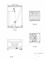
Connect the Model 851-D to a pulse generator with a
manual single-pulse capability and CRT display as shown in
Figure 4.5a or 4.5b. Depending upon the particular CRT or
oscilloscope being used, it may be necessary to use the Z
output of the 851-D for the retrace blanking signal.
CAUTION:
Some older "tube types" oscilloscopes have
a high voltage on their Z axis inputs. THIS
COULD DAMAGE THE Z OR Z OUTPUT OF THE 85~
PLEASE CHECK BEFORE CONNECTING THE UNITS
TOGETHER.
Set the units (where appropriate) as follows:
vertical sensitivity
0.1 V/div. uncalibrated,
DC coupled
Vertical position
Bottom of display
Horizontal sweep
0,1 msec/div.,
(Figure 4.5a)
Horizontal sensitivity
0.1 V/div., DC coupled
(Figure 4.5b)
Trigger input
-, DC coupled, external
(Figure 4. Sa)
Pulse Generator
Single manual pulse, 2.5
~sec wide, 0 to +3 V pulses
Set the Model 851-D as follows:
MODE:
Sample
THRESHOLD:
TTL (1.4 V)
DISPLAY:
Xl
INT. CLK.
0.1
RECORD MODE
PRE TRIG
~sec
TRIGGER:
PRE TRIG MEMORY:
100
TRIG SOURCE:
Internal
COMBINATIONAL TRIG:
CH 8 "1", all others
"X" DON'T CARE
-26-
OSCILLOSCOPE
MODEL 851-0
o
o
SIGNAL GENERATOR
CHAN 8 INPUT
EXT TRIG
VERT INPUT
(a) Triggered Sweep Display
o
@ 50 ohm feed thru terminations (OPTIONAL)
MODEL 851-0
z
Y
x
SIGNAL GENERATOR
CHAN 8 INPUT
(b) External Sweep Display
Figure 4.5
Display Interconnections
-27-
CRT DISPLAY
4.5
Operating Procedures
In this section two modes of operation will be discussed
and illustrated. A pulse generator capable of generating a
single pulse upon manual command is required.
Set the generator to give single, manually initiated
pulses approximately 5.0 ~sec wide, and 0 to +3 V amplitude.
4.51
Sample Mode
Press MANUAL ARM and pulse the generator. Figure 4.6
illustrates the display obtained. Channels 1 through 7 will
display a low level, while Channel 8 displays the pulse. The
pulse will occupy one division on the CRT, and be comprised
of 50 clock intervals. One hundred clock intervals will have
been recorded before the positive transition of the pulse.
4.52
Latch Mode
Set INT CLK to 50 ~sec.
In the SAMPLE MODE press the
MANUAL ARM and pulse the generator while watching the display.
The 851-D will trigger only if the leading edge of the internal
clock coincides with the high state of the pulse. With a 50 ~sec
clock and a 5 ~sec pulse it can be expected to take as many as
10 repetitions of the pulser for this coincidence to occur.
Now select the LATCH mode. Repeat pressing the MANUAL
ARM and pulsing the generator. Observe that the unit captures
the pulse each time and represents it with a one clock interval
of 50 ~sec. This is more readily observable by moving the
cursor near the displayed pulse and expanding the time diagram
with the HORZ-DISPLAY (EXPAND) switches. This feature is
particularly useful for detecting narrow random noise pulses
or "glitches". This mode operates in the same manner independent of the chosen clock interval. A glitch typically as
short as 5 nsec may be detected and displayed at any clock
interval.
4.53
Manual Trigger
To verify operation of each channel, change the pulse
generator to a repetitive output, approximately 5 kHz rate,
with the same pulse as before. Starting with Channell,
connect the generator to the input BNC. Press the MANUAL ARM
switch, and then the TRIGGER MANUAL switch. Several pulses
of one clock interval will be displayed on the CRT, on the top
trace. Repeat the above procedure for each channel, 1 through
7. The trace corresponding to that channel will display
several pulses in turn. The 851-D should be in the Delayed
Record mode with the trigger source set to EXT.
-28-
100 Samples
PRETRIGGER
n
t
~-------------------
TRIGGER
Figure 4.6
In the SAMPLE MODE, Channels 1
through 7 will display a low
level, while Channel 8 displays
the pulse.
-29-
SECTION V
OUTPUT INTERFACE
5.1
Introduction
The output interface of the Model 851-D includes two
methods of analog output: one, using a CRT in an X-Y mode,
and two, using an oscilloscope in the triggered mode. These
methods are explained in Section 4.41.
The instrument also offers a digital output of data.
This data is output in an 8-bit parallel format, the bits
representing a simultaneous data entry for all channels.
Five hundred twelve such 8-bit words are available through
the digital output mode.
5.2
Digital Output
All inputs and outputs at the 24-pin rear panel connector are positive logic, TTL signals. Direct access to
control gates is available at the connector. This connector
provides the physical interface for digital data output. The
connector is an Amphenol Micro Ribbon 57-30240. The mating
connector is an Amphenol part number 57-40240.
The pin assignments, and signal descriptions for the
digital interface are listed in the following table:
Pin #
Signal Name
18
19
16
17
22
23
24
21
Data Output
Data Output
Data Output
Data Output
Data Output
Data Output
Data Output
Data Output
(OUTPUTS)
2
Description
These lines supply data stored
in memory when the digital
output procedure, outlined in
Section 5.21 or 5.22, below,
Buffering is
is followed.
provided.
1
2
3
4
5
6
7
8
Line is normally pulled high.
To initiate output, pull low
to enable TTL level.
CHD
(INPUT)
-30-
Pin #
Signal Name
3
Request
(INPUT)
4
Auto Arm Mode
Description
Normally high. Changing to a low
level causes unit to "fetch" next
data word.
oV
when instrument is in Auto Arm,
..... .l-k ........... ~ ... .;,.... ........ .1-
I " 1"TrnT"l 1"Trn \
\VU·.LrU.LJ
V
1....L1C.L
vv ..L':"~;
a.
I...
_t::
')
-..J. ~
'tT
v
(f"'MilC:\
\ '-' ......."" .....
I
•
6
1 MHz Clock
(OUTPUT)
TTL signal 0.8 psec high, 0.2 psec
low.
14
Flag
(OUTPUT)
Goes high when next data word is
available, approximately 32 usec.
after request goes low.
7
M>N
(OUTPUT)
Synchronous with display output.
CMOS level, which is -5.2 V before
cursor output address and 0 V
after cursor address.
12
Display
(OUTPUT)
Low when unit is recording; high
otherwise.
9
-5.2 VDC
8
+5 VDC
11
Trigger
Logic Level Trigger input must be
brought low to enable TTL level~
I T'II.TnTTm \
\ ...LJ.'IIJ:" V.1. J
10
Remote Arm
(INPUT)
Line is normally held high and
brought low to arm unit.
1, 13
Ground
Power and logic return.
5.21
Digital Output Sequence - After Display
Immediately after recording, the 851-D will enter the display
mode, repetitively cycling the memory and producing the X, Y, and Z
display signals. In this condition, the Display (pin 12) output signal
will be high. The Dump Command
(pin 2) input is pulled high by an
internal pull-up resistor (IK to +5 V) .
To initiate an output transfer, the "DUHP COM11.AND"
line should
be brought low and held low until the desired memory transfer has been
completed. As long as the
DUMP COMr-1AND line is held low and the
Displayoutput is High, the 85l-D will be in DIGITAL OUTPUT mode. A
new recording may be initiated at any time by the record control logic
and will immediately terminate the digital output.
When in the DIGITAL OUTPUT mode, data may be transferred in two
ways; continuous transfer or single byte.
-31-
5.211
Single Byte Transfer
Each byte is initiated by presenting a REQUEST pulse (minimum
5 psec, maximum 30 psec) on pin 3. The 851-D will sequentially
assemble the 8 data bits of the currently addressed memory word and
will indicate when the data is ready by bringing FLAG high. The
data will be stable at least 500 nsec before FLAG goes high.
The next, and subsequent data words will be presented on the
data output lines after each P~QUEST (pin 3) input negative pulse.
For proper data output the interval between REQUEST inputs should be
no closer than 34 psec giving asynchronous data rates 30K bytes/
sec to DC.
5.212
Continuous Transfer
Continuous data transfer will be performed if the REQUEST line
is held low. The REQUEST line may be held low before COMMAND
is brought low. Each time a data byte is ready, the FLAG line will
be brought high for 2 usec. The data will be stable 500 nsec before
the FLAG goes high and will remain stable 500 nsec after the FLAG
goes low. The data rate will be 32 psec per byte.
5.22
Digital Output Sequence - After Record
If it is desired to output digital data immediately after Record,
proceed as follows: Hold Dump Command
(pin 2) low.
As soon as
Record is complete Oisplay goes high), the first data word can be
read. When this occurs, proceed with data transfer operation as
described above. When the desired memory length has been transferred,
return the Dump Command
(pin 2) high for further record sweeps.
NOTE:
CAUTION:
The memory of the 851-D contains 8 X 512 bits.
Only the first through 508 bits of each channel
memory are specified to be valid digital output
data.
If the ARM IN and/or TRIG IN BNC connectors
on the rear panel are enabled, Remote Arm
(pin 11) and Trigger (pin 10) must be left
floating (high).
-32-
SECTION VI
CALIBRATION PROCEOURE
601
Calibration of Display Output
Adjustments are provided to calibrate the "X" and
ny" outputs of the 851-0 to a specific output device.
If
accurate time measurements are to be made, the 851-0 and
the display device must be calibrated as a system.
Before
leaving the factory, the X and Y outputs are set at 1.0 V p~p'
(Xl) and 0.8 V p-p respectively. Figure 6.1 shows the location of the adjustments on the control board for the X and Y
levels.
Connect the 851-0 to the Oisplay as shown in
Figure 4.5.
Turn on both instruments and allow them to warm up
for at least 5 min., then proceed as follows:
1.
Remove the top cover of the 851-0 and locate
the control board. This board is located on
the right side of the unit. The appropriate
adjustments are easily made from the top.
Place
the 851-D into TTL Xl threshold mode:
2.
Locate the potentiometer marked "Y".
"-':7
~
II
~ ~
;;;;:,u
.&.. \.. _ .&..
..... ~~a......
~ _
.... \..
.;;;;a. ...... ~~
..... ~
u,!..
.&.. \ . . "
'-.L.L":;
..... ..: r r 'h ~
~..L':::'.L.L ' -
,..:...,. =
~
..L..L .... ~.....
;...,.
..L",L
Adjust
+- h
0
.... ,L,L'-
display mode are centered on each of eight
divisions of the scope face.
3.
Ensure that 851-0 expansion is Xl and that
the scope expansion is also Xl.
Locate the
potentiometer labeled "X". Adjust "X" to give
full-scale display in the horizontal direction.
The display adjustment is complete and the cover may
now be replaced on the 851-0.
6.2
Recalibration of the Internal Circuits
The following calibration procedures are intended to
be used in recalibrating the internal circuits of the 851-0.
The entire instrument was calibrated before shipment and
should not require any recalibration for at least six months
or 1000 hours of operation.
6.3
Required Test Equipment
The following test equipment will be required to
calibrate the Model 85l-0~
-33-
1.
6.4
Digital voltmeter, DC range 0-20 V
minimum, 4 1/2 digit resolution minimum.
Power Supply Adjustment
Before recalibrating any circuit in the 85l-D, it
is necessary to check the power supply outputs to ensure
proper levels. This is accomplished as follows:
1. Remove four screws in top cover.
2. Remove top cover.
3. Referring to Figure 6.1, front panel view,
connect the voltmeter between the +5 TP and the
ground TP. Voltage should be 5.00 +0.02 V.
4. Readjust R37 on regulator board if required.
5. Connect the voltmeter to the -5.2 V TP.
should be -5.20 +0.02 V.
Voltage
6. Readjust R49 on regulator board if required.
6.5
Channel 1-4 and 5-8 Threshold Adjustments
NOTE:
Effective on serial #s of 6038 and above. Units
with serial numbers below this do not have
adjustable threshold levels.
Place voltmeter on 2 VDC scale, and set the displayed
digits to 0000 with the highside connected to the low
(guard) side. This adjustment is made by the offset adjust
on most DVMs, or verify that the instrument used to set
thresholds is good to three decimal places. The meter is
in calibration on the 2 VDC scale and all threshold measurements are to be taken on this scale or erroneous data will
occur. Repeat same procedure for any scale used during test.
Connect voltmeter between CH 1-4 test jack and chassis
ground on front panel. Check levels as follows:
Threshold
Control Position
. Level at
Test Jack
ECL (black)
-1.30
+0.025 V
TTL (black)
+1.40
+0.025 V
MST (black)
0.00
+0.025 V
-0.130
+0.006 V
ECL (red)
-34-
Threshold
control Position
Level at
Test Jack
TTL (red)
+0.140
+0.006 V
MST (red)
0.00
+0.006 V
A
(red)
+0.250
+0.006 V
B
(red)
-0.250
+0.006 V
C
(red)
+0.200
+0.006 V
Readjust, using Figure 6.1 as a guide, any level that
does not meet specification.
Repeat the previous step for channel 5-8 threshold level
control and test point.
6.6
Input Offset Adjustments
Connect the DC voltmeter between pin 2 of channel 1
(AM685) L23 and ground. Voltage should record -0.012 V +0.002.
If it is not, readjust Rll3 (IOn Pot) until it does.
Repeat
this procedure for all eight channels and the EXT Clock input.
To aid in finding all devices in each channel, use schematics
and assembly drawings for main board in Section 9.
6.7
Input Capacitance
Connect a XIO scope probe from the scope calibration
signal (a 1 kHz square wave with 5-10 V amplitude) to the
Tr
..: _ _ ...
EXT "T
\"'.LJL\.
.l.llf:lU'-.
..1.-
Connect a properly compensated probe from the scope .
channel 1 to the PROBE COMP test point. Gain of channel 1
will have to be set to 0.05 or 0.02 V/cm.
Adjust the calibration signal probe for minimum
capacitance (i.e., for maximum overshoot observed on the scope.)
Adjust the input capacitance of the EXT CLK input to
compensate properly the signal, i.e. square it up.
Do not change the setting of the scope probe adjustments
for the remainder of this procedure.
Move the calibration signal probe to channel 8 and connect
the scope input probe to observe the output of the channel 8
buffer (pin 2 of the 685).
Adjust the input capacitance of channel 8.
Repeat for channel 7 - channell.
Replace top cover. This completes the recalibration
of the internal circuits.
-35-
"X" OUT
-5.2
---'------- ADJ.
CONTROL BOARD
+5
ADJ.
o
g
+
=4-1- C4
=illn=
0
ECl
u------
o
'7/
Cf?12
J
- ,
I
I
L
___
I
------J
POWER SUPPLY
REGULATOR BOARD
- 5.2 T.p.
GND
DIGITSWITCH BOARD
THRESHOLD LEVEL
., ADJUSTMENTS
Figure 6.1
Location of Adjustments
-36-
SECTION VII
TECHNICAL DESCRIPTION
7.1
General Description
The 85l-D is divided into four subsystems:
1.
2.
3.
4.
Power Supply
Front Panel
Control Board
Main Board
The power supply operates from 110 or 220 V at 50 or
60 Hz and provides +5 V at 5 A and -5.2 V at 5 A.
It also
provides a fan for cooling.
The front panel has all of the operating controls and
the circuitry for establishing the input threshold voltages.
The control board handles the display control logic
and the low-speed timing generation&
The main board has the high-speed timing generation,
the data input, the memory, and the Record control logic~
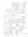
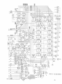
Figure 7.lA is a detailed functional block diagram.
The front panel control lines are shown along the left side.
The display outputs and the digital data interface outputs
are shown along the right side. The block diagram is divided
by a dotted line to indicate the d~vision of the logic between the main board and the control board. The main board
receives the data and processes it through the input buffers,
comparators, and latches, and stores it in the prememory.
The Record control logic (including the combinational trigger
logic, arm logic, and trigger delay counter) controls the
storage of the data from the prememory into the main memory
in response to the specified mode of operation.
The Display control logic is held reset by the Record
control logic when the data is being recorded (written into
the memory). When it is not held reset, the Display control
logic will transfer the data from the memory to the display
generator and will generate the necessary control signals
to display the data.
The Digital Data Output logic can
control logic (except when held reset by
logic) and transfer the data from memory
lines under control of the "Command" and
-37-
override the Display
the Record control
to the data output
"Request" inputs.
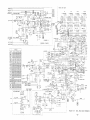
Figure 7.lB shows the physical locations of the
various functions on the main board and the control board.
The 85l-D uses three logic families: ECL 10K,
Schottky TTL, and CMOS. To achieve the desired high-speed
performance, EeL circuitry is used for all of the data
processing and the Record mode control logic. Schottky TTL
has adequate performance for the memory and is used because
it is more cost-effective than ECL memory. CMOS is used
for the control logic, where high speed is not needed,
. because of its low cost and simple interface with the ECL
circuits. The memory subsystem operates off of +5 V and
all the rest of the logic operates off of -5.2 V. Positive
logic convention is used; i.e., the more positive level is
a logic "1" and the more negative level is a logic "0".
Level translators are used for signals going to and from
the memory and for signals from ECL to CMOS. Translators
are not necessary for signals from CMOS to ECL. Figure 7.lC
shows the types of level translators used.
-38-
1---------,
I
DATA(8)
BUFFER (8) ~-----;:-~I
..
. COM~~RATOR
EXT. CLK. ..
---~"'!
r+
t
THRESHOLD
LATCHES
(8)
DATA(8)
t - - - - ; l . . - - - - - - - - - - " 1...1
~
BUFFER
AND
COMPARATOR
,I
CLOCK SELECTOR
..
I
WE
MEMORY
•
CLOCK
... CONTROL lAC.
I
I
I
~ GATE ~D-_S_A_M_P_LE_C_L_O_C_K--ii-41~..1II
I
,...
rr
I
.
..
- - - - - - - - - - - + - ;..~
COMBINATIONAL
TRIGGER
DATA..
IN'"
~
BY
8 BITS
f---+~----ADDRESS
I- -
~
I
~
,~. 4~
L.--_-+_ _ _---:-,_--,
L
RECORD/DISPLAY
EXT.TRIG.
~
ADDRESS
CONTROL
I
1_ i
MEMORY
512 WORDS
r-.L------J
'--_---.J
~~
M:~6R~
WE
I
I ....
I.~
TRIGGER SELECT
EE~~1IL
PC.. TRANS
L - -_ _- - - - '
~
I
--..
r - - -......- - - - - - , -
t
-
-
-
i
I
-
OUTPUT BIT
SELECTION
1
DATA OUT
---I
'L-E-VEL-TR-ANSLA-T-ORS-' I -
ICMOS
~~~~-~A~--~~r~-----r~
EXT. ARM
lr
MAN. ARM
RECORD CONTROL
LOGIC
I _
CLOCK
GENERATOR
(ECL)
LJ
I
.
~~---r__'
I
.
~~--~---_T~
PRESET
100 MHZ ~
CRYSTAL 0
ARM OUT ..
INTCLKOUT--:
~~
..
9'S
DELAY VALUE
------------~~~ICOMPLEMENT~
...
TRIG OUT ..
..
RECORD MODE SELECT
A~END
OF
DELAY
'I'
END OF
RECORD
SAVE
II
i
-- -- ~
DELAY
COUNTER
PRE1SET
I
~-----"
i
I
1
~
-
-
DATA
i
ECL/CMOS
TRANS.
CLOCK
GENERATOR
CMOS
DATA DISPLAY
CHANNEL SELECT
DISPLAY
GENERATOR
AND
DRIVER
SEQU~NCER
rL-.-..--.,--I
BLANK
DISPLAY CLOCK
1 KHZ
500 KHZ
DISPLAY CLOCK
LOGIC
X1
MIXED
ENDOF
DATA
ENDOF
DATA FIELD
COUNTER
DATA
EXPANDED
X5
X10
CURSOR POSITION
CURSOR MARKER
X20
LEFT
RIGHT
CURSOR SPEED
CONTROL
CURSOR POSITION
UPIDOWN COUNTER
OUTPUT MODE
MEMORY DATA
Figure 7.1A
I
.I
TTL
851-0 Detailed Functional
Block Diagram
DIGITAL DATA
OUTPUT LOGIC
500. KHZ
CMOS
-39-
TTL
MAIN
BOARD
'fCONrROL
BOARD
Y ADJUST
PHYSICAL LOCATION 851-D
X ADJUST
....J
>-0
«0::
DIGITAL ~
INTERFACE
FRONT
PANEL
INTERFACE
TIMING GENERATION
....Jt-
Q..z
CONTROL LOGIC
!:a 0
QU
XTAL
RECORD CONTROL
LOGIC
TIMING GENERATOR
CJ)
0::
>0::
0
MEMORY
2
W
2
W
0::
I
~
Q..
z
«
0::
t....J
W
>
W
WQ
2«
Figure 7.lB
0
t«
....J
CJ)
....J
<.?
0::
t....J
«CJ)
zw
0:C
-u
t-t-
««
Z....J
iii
CJ)
0::
O
t-
«
0::
«Q..
2
0
-40-
::>
OJ
t-
::>
t-
Z
::>
U
Z
Q..
Physical Locations on the Main Board
and the Control Board
o::
W
u..
u..
U
2
0
CJ)
Q..
A) ECl to TTL
B.) TTL to CMOS
+SV
47K
10125
EC_l__
C.) ECl to CMOS
~~~---TTl----~~~~~
ECl
CMOS
4069
4069
-S.2V
-S.2V
Figure 7.1C
Level Translators
-41-
7.2
7.21
Detailed Description
Front Panel
The front panel assembly consists of two printed circuit
boards and the front panel. The boards are called the "front
panel board" and the "digitswitch board." The front panel board
provides the mounting and interconnection of all of the control
switches except the trigger delay digitswitch. The interconnection
of the front panel switches to the control board is done by a PC
edge-card connector between them. The combinational trigger selector switches are connected directly to the main board by a
l6-conductor flat cable that plugs into a socket on the main
board.
The digitswitch board contains the digitswitch and the
threshold voltage circuitry. The threshold selector switches
are connected to the digitswitch board by a 3D-conductor flat
cable that is soldered to both boards. The threshold levels
are returned to the front panel board by that same flat cable
and then passed to the control board by the edge-card connector
and, in turn, passed to the main board by J2 of the control board.
The delay selecting digitswitch is connected from the digitswitch
board to the main board by a 16-conductor flat cable that is
plugged into a socket mounted on the main board. Test points
are provided on the digitswitch board to monitor the supply
voltages and the threshold voltages.
The two boards are connected to each other by the 30conductor flat cable, and normal servicing is done by using that
cable like a hinge and opening the boards. If the boards are to
be operated in this position, a ground connection MUST be provided
between the two boards.
The threshold voltage circuit is shown in the schematic
in Section IX. Resistors RIO and Rll drop the voltages supplied
to Rl, 2, and 3 to about +2.5 V and -2.5 V. The thresholds for
these positions (TTL, ECL, MST) can be set anywhere between these
voltages. This provides thresholds for use with Xl probes. The
thresholds for use with XIO probes are set by R4, 5, 6, 7, 8, 9.
To provide greater resolution for these adjustments the voltages
supplied to the resistors are reduced to +0.5 V and -0.5 V by
the circuits of Ul, R12, R13, R14, and R15. The front panel
variable threshold uses a circuit similar to that of Rl.
7.3
Control Board
Refer to the Control Board Schematic in Section IX
for the control board description. With the exception of the EeL
to TTL level translators, the control board is all CMOS circuits
-42-
and the logic levels ~ncountered will be 0 V for logical
one and -5.2 V for logical zero.
The timing generation is divided into two parts. The
main board contains the high-speed timing and provides the
control board with a I-MHz clock. The control board then divides this clock down to provide 100-kHz, 10-kHz, I-kHz, and
, n n
The control board receives the time base
.LVV-O:£.
selector switch signals from the front panel board, and the
logic generates control signals that go to the main board to
select the desired clock signal for the data sampling clock.
The display control logic uses the SOD-kHz clock as the basic
data output clock and the I-kHz clock for the display horizontal
sweep rate. The horizontal sweep is generated as a l-msec ramp
of I-V amplitude with a l-msec blanking time between sweeps.
The amplitude of the horizontal sweep is adjusted by R26 from
0.7 to 2.5 V. The l-msec blanking time allows for retrace time
in the display when an oscilloscope is used in the triggered
sweep mode. The display blanking signals Z and Z are generated
by the counter AS as a square wave with 1 msec on time and 1 msec
off time. The counter AS controls the display sequence by
simply counting the I-kHz clock.
TT _
_..: _ _ _ ,
,..
~.L':::1ua..L~.
The display sequence is:
AS
0123
Count
0000
0
8
Bla.nked
1000
1
8
Data displayed with 0 V offset
(normally at the bottom of the
display)
0100
2
7
Blanked
1100
3
7
Data displayed with 0.1 V offset
0010
4
6
Blanked
1010
5
6
Data displayed with 0.2 V offset
0110
6
5
Blanked
1110
7
5
Data displayed with 0.3 V offset
0001
8
4
Blanked
1001
9
4
Data displayed with 0.4 V offset
0101
10
3
Blanked
1101
11
3
Data displayed with 0.5 V offset
Channel
Selected
-43-
Display
AS
0123
Count
Channel
Selected
Displa:l
0011
12
2
Blanked
1011
13
2
Data displayed with 0.6 V offset
0111
14
1
Blanked
1111
15
1
Data displayed with 0.7 V offset
0000
0
8
Blanked
1000
1
8
Data displayed with 0 V offset
0100
2
7
Blanked
The display driver for the vertical axis (Y axis) consists
of an op amp B3 with an output buffer transistor Ql to provide
increased output drive. Resistor R40 is provided to damp potential ringing on the output cable. The output may be modified
to drive a 50-~ input by changing R40 to a lower value (typically
10 ~). The amplitude of the vertical output may be adjusted by
R25 from 0.75 to 1.25 V full scale. Capacitor C9 provides some
additional frequency roll off to shape the vertical edges of the
data display. The display vertical position is determined py the
sum of the currents introduced to the summing junction by the
logic. Because of the simple resistive output characteristics
of the CMOS gates, the hex inverter B6 is used to switch the
input resistor either to ground (for no current) or to -5.2 V.
7.31
Display Mode Control
The display mode control logic is held at reset whenever
the 851-D is recording. The record mode control logic on the
main board supplies the signal "Record Mode CIt to the control
board for this purpose. The display mode logic becomes active
whenever this signal goes low. The flip-flop of C9 provides
a synchronized start up of the display mode with the I-kHz
clock. On the first I-kHz clock after Record goes low, the
output of C9 pin 15 goes high, and the signal SAVE B is sent to
the main board to save the memory address at which the record
mode ended. Also, a pulse is generated by C18 and R41 to
initiate the memory address preset cycle. On the second I-kHz
clock, the output C9 pin 1 goes high, and the counter AS is
allowed to begin normal display sequencing. The display sequence
will always start at count zero because the counter is held reset
during record mode.
-44-
A "blank" cycle always precedes a display cycle. At the
beginning of every blank cycle, a pulse is generated by CIO and
R35 that will preset the flip-flop Al4B (and also flip-flop Jl
on the main board) to start the memory address preset cycle.
The signal PRESET ADDRESS will remain high for five clock cycles
of the 500~kHz clock and will allow the memory to be clocked
five times to preset properly the memory address.
Figure 7.2
shows timing diagrams for the memory clock operation in the
display modes Xl, MIXED, EXPAND.
N = EXPANSION CTR.
M = MEMORY CTA.
I
~------BLANKED--------~~------UNBLANKED------~
(a)
X1
CLOCK
M;:::N
PRESET B
PRESET ADDRESS
(b) MIXED
CLOCK
SEE FIGURE 7.11
(c) EXPAND
CLOCK
Figure 7.2
Display Memory Clock Generation
In Xl mode, the memory is clocked five times at the
beginning of the blanking cycle, and then no more clocks are
generated until the display is unblanked. At this time, the
memory is clocked at the 500-kHz rate for the entire display
time. This provides exactly 500 clock pulses during the display
in Xl mode. The memory address is then preset again at the
beginning of the next blank time.
-45-
In MIXED mode, the memory address is preset as in Xl mode,
and then no more clock pulses are generated until the display is
unblanked, at which time the memory is clocked at the SOO-kHz
rate until the memory position counter (AlO, All, and A12) is
equal to the cursor position counter (ClO, Cll, and C12). At
that time the clock rate is changed to either 100 kHz, 50 kHz,
or 25 kHz depending on which expand is selected on the front
panel (XS, XlO, or X20). The circuitry for generating these
clock rates is shown on sheet 1 of schematic 0852-0011 and
consists of A20, B20, B2l, B22, and parts of B19, C19, and AIS.
The counter formed by A20 and B20 is programmed by the select
logic to divide the SOO-kHz clock by either 5, 10, or 20 and
then enable the SOO-kHz clock for a single clock. Refer to
Figure 7.3.
500 kHz CLOCK
M~N
0
DISPLAY CLOCK
(X5 MODE)
3
JL.J1.JLflJ
JLI1..J1...JL.J
Figure 7.3
4
0
2
3
U
0
(X10 MODE)
2
2
3
4
4
U
5
6
7
8
9
U
Memory Clock Details in MIXED Mode
In EXPAND mode, the memory address is preset at the beginning of the blank cycle, and the memory is then clocked at
the SOO-kHz rate until the memory position counter equals the
cursor position counter, at which time the clock is disabled
until the display is unblanked. Then, when the display is
unblanked, the memory is clocked at the rate determined by the
selected expand (XS, XlO, or X20) as described above.
7.32
Cursor Position
The cursor position counter is shown on the schematic
in Section IX and consists of A17, A16,' A18, A19, B13, BlS, B16,
B24, ClO, Cll, C12, C13, and C14. The cursor position counter
is an up/down counter and is controlled by the horizontal
position switch on the front panel. When the switch is pushed
to the right, the counter will be counted up, and when the switch
is pushed to the left, the counter will be counted down. A
contact bounce elimination circuit is used to condition these
inputs to ensure proper operation. The flip-flops B24A and
B24B sample the switch contacts at a 100-Hz rate and ensure the
elimination of any bounces in between samples. Counters A16
and A17 are held preset to 4 counts less than top count (TC)
until the switch is activated.
-46-
When the switch is activated, in either direction, the
counter is allowed to count. When the count reaches TC, a
single pulse will be allowed to count the cursor position up or
down. The counters will then continue to count until A16 reaches
count 2, at which time A16 will be stopped and the cursor position counter will be continuously clocked, at the selected
rate, until the switch is no longer activated. Refer to Figure 7.4.
If the switch bounces or is released, the counter will be preset
again and the process must be started over. This gives a cursor
"hesitation," allowing the operator to reliably achieve a single
count. The rate at which the cursor position is clocked is determined by the circuit in such a way as to give a constant rate
of motion of data on the display (2 cm/sec on an 8xlO dispiay) in
expand mode regardless of the selected expand.
100 kHz
SWITCH INPUT
PE A17-9
---I
COUNTER A17 '-13113(141151011 234567891011 12 1314150 1 2 3456789 10 11 12 13 14 15 0 1 23456
COUNTER A16 4-151
A16-10
CET
A16-15
CU (OR CD)
151--
-I"
0
1
-I"
2
-4-1-------------------------:..______
TC
X1 MODE
X5 MODE
X10 MODE
I---~
~----J
1--------'
X20MO~
Figure 7.4
"---___--II
Cursor Position Logic
In Xl mode, the rate is 100 Hz, in X5 mode the rate is
25 Hz, in XIO mode the rate is 12.5 Hz, and in X20 the rate is
6.25 Hz. These rates are not exactly the same as the X5, 10,
20 expand ratios. They are, instead, X4, 8, 16 because it is
much simpler to use a binary counter, and the slight change in
apparent data motion speed is not noticeable.
-47-
A power-on reset circuit C12 and R36 resets the cursor
position to zero (off the left side of the display) when power
is turned on. When the cursor position is at zero, any attempt
to count it down will cause a signal on the reset line and will
prevent it from going past zero. Similarly, when the counter
is at count 511 it will not be allowed to count up.
By allowing the memory position counter to count the
memory present clocks at the beginning of each blank cycle, the
cursor appears to be positioned 4 counts to the left of the
beginning of the data. This allows the cursor to "disappear"
by positioning it off the left side of the display.
It also
means that it will not be seen on the screen until the fourth
pulse.
7.33
Digital Data Interface
The digital data interface uses all TTL signals. The
control logic and output logic is on Figure 9.7 in Section
IX. Because the memory is organized to read out a single data
bit at a time, it is necessary to sequentially read out the eight
data bits and shift them into a shift register C2 to provide a
parallel output. The counter AS is used to control this
sequential operation.
Refer to the timing diagram in Figure
7.5. THE DU~~ CO~wrnND input is active low. When it is active,
it will allow the flip-flops of B9 to initiate the dump operation.
The first clock pulse of the SOD-kHz clock after Command goes
low will set B9 pin 14 low, and this will enable the output
shift register and the control logic for AS. This will generate
a memory address preset signal.
500 kHz
COMMAND
REQUEST
DUMP ENA8LE 89-15
89-1
DUMP PRESET
PRESET 8
DISPLAY CLOCK
CEP A5-7
I01 23456789 10 11 12 13 14 15r--__
COUNTER A5 STATE
TC A5-15 --------/ /------------------------'
--I 1--__---.
DUMP CLOCK ------~ ~------------------~
FLAG ------~ ~--------------------~
SHIFT REG CLOCK C2-6
Figure 7.5
Digital Data Output
-48-
The memory address preset will generate five clocks to the
memory in the same manner as during normal display operation. The
second clock of the 500-kHz clock will cause B9 pin 1 to go high
and pin 2 to go low, will remove the memory preset signal, will
enable the 500-kHz clock to A5, and will disable the I-kHz clock
from A5. The preset address signal on A14 pin 15 will hold A5
reset until the memory preset cycle is complete.
When the REQUEST LINE is brought low, the counter A5
will be enabled by the latch circuit of A9. This will sequentially
read out the eight bits of data and shift them into the shift_register(C2). When A5 reaches count 15 (TC), it will reset the
latch circuit (A9), thus disabling the counter (A5). The TC signal
is translated to TTL level and output as the FLAG signal.
If the request line is held low continuously, the counter
A5 will begin a new data output cycle on the next clock (500 kHz)
after FLAG (or TC)goes true.
In this mode a new data word will be
output every 32 ~sec.
The output data may be clocked with the leading edge of
the FLAG signal. The output data will be stable at least 500 nsec
before the FLAG signal goes high and will remain stable for at
least 500 nsec after the FLAG signal goes low.. The input control
lines COMMAND and REQUEST are translated from TTL to CMOS by
Schmidt Trigger level translators A4 as described in Section 7.1.
7.34
Display Synchronization
A display sync input is provided in the digital interface
connector (pin 15). To sync the display of two 851-0 instruments,
all that is necessary is to connect the ~ output of the "master ll
unit to the display sync input of the "slavell unit. The positive
going transition of the display sync input will generate a pulse,
and if the 851-0 is in display mode, this pulse will reset the
counter chain of A21, A22, A23, and A24. This will cause the
two instruments to run in sync.
7.4
Main Board
Refer to the main board schematic in Section IX.
7.41
Input Buffer
The input buffer circuits are the same for all eight data
channels and the external clock input. Operation of data channel
one will be described.
Resistors RIOI and RI02 and diodes CRIOI and CRI02
establish the input impedance at 1 MQ and also provide protection
against input voltages as great as 100 V for short duration, 50 V
continuous. The main limitation on the input protection is the
power dissipation in RI02. Capacitor CI02 provides frequency
compensation for RI02. Capacitor CIOI allows adjustment so that
all inputs have the same capacitance. QIOl, RI05, RI06, and Rl13
make a zero offset FET source follower circuit.
Rl13 allows
fine adjustment of the offset voltage.
-49-
7.42
Comparator
Diodes CRl03 and CRl04 protect the inputs to the comparators and clamp the voltage to approximately +3 V. The
clamp voltages are generated by the op amps A25A-and A25B and
resistors R20, R2l, R25, and R26. The nominal values of the
clamp voltages are +2.6 and -2.5 V. Resistors Rl03 and Rl07
provide hysteresis. Because the outputs of the comparator
are ECL signal levels (-1 and -2 V), the hysteresis circuit
introduces an offset error of approximately 10 mV, and this
must be corrected by the adjustment of the input buffer offset
Rl13. The comparator provides complementary ECL outputs, and
resistors L20-l4 and L20-l3 are the pull-down resistors.
7.43
Latch/Sample
The Latch/Sample circuit is formed by flip-flops L18A
and L18B as well as gates L2l, and is controlled by the signal
SAMPLE MODE ENABLE from the front panel switch. When the signal
is high, the circuit is in sample mode, and when it is low, the
circuit is in latch mode.
In sample mode, the gates L2l are
disabled and their outputs are low. This allows the first flipflop L18A to operate in the clocked mode, and the data present
at the input at the time of the positive clock transition will
be clocked into the flip-flop. The second flip-flop simply
passes the data on one clock pulse later.
In the latch mode, the gates L2l are enabled, and the
first flip-flop acts as a latch that changes its output whenever
it detects that the input data is different than it was at the
last clock transition (as stored in the second flip-flop) .
Figure 7.6 shows the operation for several different inputs.
SAMPLE CLOCK
Figure 7.6
7.44
Latch Mode Operation
Combinational Trigger
The Combinational Trigger circuit is L16, L17 (and the
same gates on the other seven channels), A8, A7. Gate L17 will
-50-
generate a low output if the data on L18 output is high and the
selector switch is in the "1" position or if the data is low and
the switch is in the "0" position. 'rhe combinational trigger
gates L17, K17, J17, H17, F17, E17, D17, and C17 are all connected
together in a "wired-ANDn such that the selected trigger conditions of all eight channels must be true for the signal TRIGGER
NODE to go low (true). The flip-flops A8A and A8B provide two
functions.
The first flip-flop synchronizes the data to the
sample clock and eliminates the propagation delay effects of the
"Trigger Node. II The second flip-flop allows the detection of
Trigger Node transitions by the gates A7.
Either positive or negative transitions are selected by
the front panel switch "INT Tn or "INT F."
7.45
Timing Generation
The internal timing generator is shown in Section IX
and consists of the crystal Yl, Ri2, R23, Ll, C24 r C4l~ and the
ICs A24, A23, A22, as well as the level translator Q5.
The
resonant circuit formed by Ll, C24, and C4l is to ensure that
the crystal does not operate at one of its lower harmonics.
The crystal operates at the sixth overtone.
Resistors R22 and
R23 provide bias for the gate A24.
Resistor R24 is simply a
pull-down. The complementary output (pin 9) of A24 is used to
avoid loading effects on the oscillator. The counters A22 and
A23 simply divide the oscillator by 10 and 100 to provide the
la-MHz and I-MHz clock rates.
The gates of A20 are used to select between 100 MHz,
10 MHz, 1 MHz i and 100 kHz; and gate A24 selects the low-speed
clock rates from the control board. The flip-flops A18 and
A19 generate rates of one-half and one-fifth of the selected
clock. Then the gates of A16 select the 1, 2, or 5 division as
specified by the control board. Gates A15 and A24 allow the
selection of INT, EXT!, or EXT\.
Gate B19 is used to drive the
coax cables to distribute the clock to the input latches.
7.46
EXT ARM/EXT TRIG
The inputs for EXT ARM and EXT TRIG are especially configured to allow either TTL or ECL inputs.
Because the ECL
and TTL input circuits are wire-or'ed, only one of them may be
active at a time.
(The other one may be left-disconnected.)
The EXT TRIG input stage operates in the following manner.
TTL input is applied to pin 11 of the digital I/O connector on
the rear panel. The signal is passed from the control board to
the main board by Jl-E to resistor R43 and the base of Q3.
R43
is a pull-up resistor to +5 V and will maintain the input inactive (high) when no input is connected. The resistors R44 and
R45 establish a bias point of +2.5 V on the emitter of Q3 and
-51-
set the input threshold level. As long as the input is higher
than +2.S V, Q3 will be off and will not affect any signal that
may be input on the ECL input. When the TTL input goes low,
then Q3 will conduct and its collector current will be set by
R44 and R4S (typically 20 rnA for an input low level of O.B V) •
This current will raise the voltage of the input pin 11 of CB
to about -1.0 V as a result of resistors R3 and R4, which form
an equivalent termination of SO Q to -2.0 V. For ECL input
signals, the termination of R3 and R4 will correctly terminate
an ECL output driving a SO-Q cable.
The EXT ARM input stage operates in the same way as the
EXT TRIG input.
7.47
Memory
The memory subsystem is multiplexed to achieve the required writing rate of SO MHz.
The result of this is that the
memory ICs only have to operate at 2S MHz because the data is
alternated between two memory ICs.
The memory multiplexer operates as follows.
In record
mode, the sample rate clock is applied to both flip-flops of
B16, and these flip-flops are connected to change state on every
positive transition of the sample clock. The data holding registers (referred to as prememory) are clocked by the signals PCl
and PC2 from the level translator BlS. Because PCl and PC2 are
complementary signals, the data registers will be clocked
alternately by the positive edges of the sample clock.
A typical operation would be: At the positive edge of
the sample clock, the flip-flops are set such that PCl goes
true and PC2 goes false.
The data will be strobed into the
prememory 1 by PCl and the previous data, already strobed into
prememory 2, will be written into the memory by the signal WE2.
On the next positive edge of the sample clock, PCl will go false
and PC2 will go true. The new data will be strobed into prememory 2, and the data already stored in prememory 1 will be
written into the memory by WEI.
Thus, on each clock, the new
data is stored in the prememory, and the previous data is
written into the memory.
The memory address operates in a similar manner.
On the
same clock that sets PCl true, ACI is also set true, and AC2 set
false.
When ACI goes true, the address is stored in addressholding register 1 and the address counter is incremented~ On
the next clock, AC2 goes true and stores the new address in
address register 2. The newt clock will store that address in
register 1 and increment the address again.
Thus, the data and
address registers for memory 1 are both clocked together and the
write enable pulse for memory 1 is brought active on the next
clock pulse. The level translators for write enable and chip
select are gated on and off by a resistor network R17, RIB, R41,
-S2-
and R42. When RECORD MODE is low, the level on pin 11 of B15
is -1.3 V and the translator functions normally. When the level
is high, pin 11 is at -0.66 V, and the outputs are held high.
During record mode the chip selects are both held low.
In display mode, i.e., when not recording, the write
enable level translator is disabled and forced to high outputs.
The level translator for the chip select is enabled to allow
alternately selecting the memories for readout. The memory
address clock is switched from the sample clock to the "display
clock" by simply disabling gates B18, forcing flip-flop ClO to
follow the sample clock during record mode. The display clock
is generated by the control board and flip-flop ClO to provide
the multiplex action. The chip select signals CSI and CS2 are
active low and operate in much the same way as the write enable
signals during record mode. For example, on the positive edge
of the display clock, ACI will go true and AC2 will go false,
and the memory address will be incremented. On the newt positive edge, AC2 will go true and CSI will go false, the address
will be clocked into memory 2, and the data will be read from
memory 1 until the next clock. At the next clock, the address
will be clocked into memory 1, the address will be incremented,
and the data will be read out from memory 2. The data is
alternately read from memory 1 and 2.
To be able to restart the memory at the correct memory
address, the "end of record" address must be saved. Both the
memory address counter and the memory multiplexer phase are
necessary. The signal RECORD MODE is connected to B16 pin 6
so that when record mode ends the flip-flop will be disabled.
rphnQ
mnl+;nlAv
nh;:::!c::::.A will
hA
;n +h;c::::.
- . . . --,. +hA
- . . . - .....
----.1:'""--.. - .1.-----.. --- - m;:::!;n+;:::!;nAn
-.. ----------- ------- fl;n-flr.n
---.1.- ---.1.until record mode starts again, and, because the address counter
is clocked by this flip-flop, the address counter will be stopped .
. The memory address must then be saved in registers L2 and K2
before the display clock is initiated. The signal SAVE A is
generated by the control board and strobes the memory address at
the end of record into the register. To restart the memory, it
is necessary only to transfer the memory address from the registers to the counter and to preset flip-flop ClO to the state of
flip-flop B16. Because the counter has a synchronous preset, it
is necessary for flip-flop Jl to hold the preset enable on the
counter until it is preset by clock ACI.
7.4-8
Record Control Logic
The record mode cont~ol logic is shown on the schematic
in Section IX and has three major control signals: Am·lliD,
ENABLE DELAY COUNTER, and RECORD MODE.
The control signal ARMED is generated by A4 pin 15. The
ARMED signal may be activated at any time by the manual arm
switch or by the TTL external arm input, which is the ECL external
-53-
arm input.
It may be activated by the auto arm signal if it is
not already armed and the delay counter is not enabled. The
circuit is latched in the ARMED condition until a trigger signal
is received and the delay counter is enabled, at which time the
ARMED latch is reset. The output of A3 pin 7 is connected to
B5 pin 13 and prevents the acceptance of a trigger signal as long
as the manual arm or the external arm signals are active.
The ENABLE DELAY COUNTER signal is activated (set true)
by the trigger signal applied to B5 pin 10.
It is reset by the
"end of record" signal applied to BS pin 11, and is clocked by
the positive edges of the sample clock. When the delay counter
is enabled, BS pin IS goes true and causes the ARMED latch to
be reset, the auto-arm signal to be disabled, and the delay
counter to be changed from preset mode to count-up mode.
At the same time, BS pin 14 goes false and enables gate
AS to generate the start record mode signal when in the delay
trigger mode. The "end of record" signal is generated by gates
B8 and C8 depending on the mode selected (pretrigger or delayed
trigger). For pretrigger mode, the end of record signal is
decoded as count S08, and for delayed-trigger mode the count Sll
is decoded.
The delayed-trigger counter uses flip-flop CIO to generate
the "ripple" clock for counters BIO, BIl, B12 because the carry
out signal has too much propagation delay for operation at SO MHz.
However, because the preset is synchronous (requires a clock),
during preset mode it is necessary to gate the flip-flop inactive
(by holding it preset) and to introduce the sample clock to drive
these three counters.
The RECORD MODE signal directly controls memory for recording and allows the control board to generate the display
control signals when not recording.
RECORD MODE is set true
in pretrigger mode whenever the signal ARMED is true.
In delayed trigger mode when the delay counter is enabled and reaches
TC , the same thing occurs.
The delay counter in delay mode will be preset to a value
that will require the selected number of clocks after trigger
to reach TC. This preset number is generated by taking the
"tens complement" of the front panel digitswitch. Circuits A9,
AIO, All, and A12 perform this function when delay trigger mode
is selected. When pretrigger mode is selected, they present the
digitswitch information to the counters unchanged.
7.S
Power Supply
The power supply is a series pass type and has foldback
current limiting and overvoltage crowbar protection. The circuit
will maintain regulation with only a 0.6 V drop from input to
-S4-
02
RECTIFIED
AND FILTERED
DC
R10, 11,21,22,41,42,47
PASS
TRANSISTOR
CURRENT
SENSE
RESISTOR
NETWORK
+50UT
CURRENT
LIMIT
UI-D
AMP
DRIVER
TRANSISTOR
05
OVERVOLTAGE
CROWBAR
PROTECTION
OUTPUT
SENSE
NETWORK
ERROR
AMPLIFIER
UI-C
R43,44
I+
cb
1 25V REFERENCE
I'
VOLTAGE
UI-AAND
UI-8
-: j=-
I
I
1
-
I
I
I
I
I
I
I
I
GND
I
I
, DRIVER
,
, I'RROR ,..
OUTPUT
TRANSISTOR f+- AM"piji=iER t"I-I-------------~
SENSE
U2
NETWORK
R27,30,49
06
-
OVERVOLTAGE
CROWBAR
PROTECTION
CURRENT U2
LIMIT
tAMPLlFIER
r--.
PASS
--~TRANSISTOR .---~
01
CURRENT
SENSE
RESISTOR
NETWORK
R3,4,7,16,25,26,29
Figure 7.7
Power Supply Block Diagram
-55-
•
• -5.2 OUT
output, thus enabling the supply to achieve good efficiency.
Figure 7.7 is a simple block diagram of the regulator circuit.
The negative regulator is very similar to the positive regulator
and is connected so that the negative output tracks the positive
output. There are two adjustments for the output voltages.. The
positive output is adjusted by potentiometer R37, and the ratio
of the negative output to the positive output is adjusted by
potentiometer R49.
Figure 7.B is a simplified schematic of the positive
regulator circuit. The configuration of the pass transistor Q2
and the driver transistor Q5 is especially chosen to allow
operation with the minimum voltage drop from input to output.
The resistor RIB is necessary to limit the base current to Q2
during turn on and in case of very low input voltage. A
Darlington transistor is used for Q5 to provide sufficient
current gain to drive the pass transistor into saturation at a
5-A output. The pass transistors are mounted to a heat sink
directly in front of the fan and are electrically insulated from
the heat sink. The driver transistors are mounted on a small
heat sink on the printed circuit board and are also insulated.
+ DC IN
Q2
2N3789
----------~----~
+50UT
~----------------------------~---------------------
R18
C17
0.001 J.L F
5!1,5W
9
10
1------1---
Figure 7.B
VREF = + 1.25V
Simplified Schematic - positive Regulator
The reference voltage circuit consists of two op amps and
a monolithic dual diode.
Refer to Figure 7.9. The dual diode
eR9 provides a temperature stable reference in the following way.
-56-
The reference voltage circuit makes use of the temperature
tracking of the two diodes and, by setting the current level in
each diode properly, achieves a cancellation of the temperature
coefficients of the two diodes.
+DC IN - - - . ,
7
t ?Ig:7. .
/3_5_V_ _..
CR14
IN4152
R32
1K
r=t-- -,
I
I
R37
I
5000
VREF ADJ
IMSD6100
L__
CR9
Figure 7.9
1
sf I
A
I
-.J
-
Schematic - Reference Voltage
To provide reference stability with respect to input
voltage changes, a current source is formed by the op amp Ul-A
and resistors R3l, R32, and R40. This provides a constant 20 rnA
to diode "B." The reference voltage output as a function of
input voltage is shown in Figure 7.10.
1.2V
o
1
2
3
4
+ DC IN
Figure 7.10
5
6
7
8
9
10
(VOLTS)
Reference Voltage Versus Input Voltage
-57-
In normal operation, the op amp UI-C compares the
reference voltage to the feedback voltage (from R44 and R43)
and controls the driver transistor Q5 in such a way as to
maintain the output voltage at the desired value.
If the output is low, the op amp UI-C will go more positive and cause Q5
to -pull more current from the base of Q2, thus causing Q2 to
provide more current to the output to raise the voltage. The
resistor R9 provides current to the output to ensure startup.
The current limit circuit consists of op amp UI-D and
resistors RIO, Rll, R21, R22, R41, R42, R47, R48, CR8, and CR13.
The circuit acts as a differential comparator and when the
voltage across RIO and Rll reaches the value determined by R21,
the op amp will go positive and force the regulation to be controlled by the current limit circuit UI-D. The typical values
of current limit are 9 A (450 mV) for +5 output and 6 A (300 mV)
for -5.2 output. The diode CR13 and resistor R48 introduce
additional current to the network to increase the current
allowed at low-output voltages. This ensures startup. The
resistor R50 in the negative regulator performs this same
function.
The overvoltage crowbar circuit consists of Q4, CR6,
R23, and C6 as shown in Figure 7.11. The SCR Q4 will be triggered
when the output voltage reaches CR6 plus the gate trigger voltage
of Q4 (about 1 V). This value is typically 7.2 V. This circuit
is intended to protect the system in case of a failure of one of
the pass transistors.
If Q2 fails, the output voltage will rise
until it reaches about 7.2 V, at which time the SCR will be fired
and draw the output voltage down to about 0.9 V. Because the
transistor Q2 has failed as a short circuit, the current limiting
circuit will not function and the current drawn by Q4 will be
determined by RIO, Rll, and the wiring resistance. This will
normally be a large current (>10 A) and will cause the fuse to
blow.
+5 OUT
CR6
IN753A
6.2V
Q4
T2800D
C6
R23
62!}
+1>
35V
Figure 7.11 Overvoltage Crowbar Circuit
-58-
Provision for selecting the nominal line voltage of
100, 120, 220, or 240 V is provided in the AC power-plug unit
on the rear panel. Also included in the AC power-plug unit is
an RFI filter.
The transformer is specified for operation from
50-to 400-Hz line frequency.
The power supply includes provision for remote sensing
of the output voltages to .eliminate the effects of voltage
drop in the connecting lines.
Resistors R46, R28, and R35 are
included to establish the sense voltage in the event that the
remote sense lines become disconnected.
In this case the output
voltages will increase by about 0.1 V.
-59-
SECTION VIII
MAINTENANCE PROCEDURES
8.1
Maintenance
This section covers maintenance and disassembly procedures for troubleshooting and repair of the Model 851-D. Repair is performed with the aid of a diagnostic procedure for
the unit, a technical description, and a schematic diagram.
Waveform photographs have been included with the schematics to aid service personnel who wish to troubleshoot to
the component level. Additional assistance in a particular
problem can be obtained by contacting the Customer Service
Department at the factory: Phone (408) 988-6800 TWX (910) 338-0509.
In summary, there are two methods of service available:
8.2
1.
Return the entire unit to the factory or service
center for repair.
2.
Troubleshoot the problem to the component level
with the aid of the troubleshooting procedure and
schematics or with the aid of factory personnel.
Required Test Equipment
The following test equipment will be required to conduct
the diagnostic procedure:
1.
Two pulse generators capable of <l-nsec rise and
fall times. A minimum pulsewidth of 2 nsec of
output adjustable from -5 to +5 V into 50 Q with
single pulse capability.
2.
An oscilloscope: 2 channel DC to 200-MHz input
bandwidth. Horizontal resolution to 1 nsec.
3.
Digital voltmeter:
digit resolution.
4.
A frequency counter, range 1 to 100 MHz min.
Range 0-20 V min, 4 1/2
If a display device is not normally used with the
Model 851-D, an additional oscilloscope or CRT display will
be required during the testing period. This latter oscilloscope need only have a 2-MHz input bandwidth.
-60-
8.3
Diagnostic and Troubleshooting Procedures
DIAGNOSTIC PROCEDURE
8.31
Equ~pment
TROUBLESHOOTING PROCEDURE
Setup
Connect a display device to the
851-D as per Figure 4.5. Turn
on the 851-D and the display and
allow them to warm up for a few
minutes.
NOTE:
Display may not
be present at
this time.
Set Front Panel controls as follows:
Trig Source - Int (T)
Record Mode - Delay Man
Delay - 0000
Threshold - TTL Xl Both CH 1-4 and
CH 5-8
Int Clk - 0.02 ~sec
Clock Source - Int
Display - Xl
Press MAN ARM switch down. ARM
ready light should come on. Press
Man Trigger. Display should now
look like Figure 8.1.
Arm light not illuminated.
Verify ECL Logic Low at IC
A4 pin 14 (test point 31).
Observe <-5.2 V DC at test
point 63.
No display when triggered.
Verify ECL Logic High at IC
B5 pin 3 (test point 30).
Observe 1 msec square wave
at IC AS pin 14, and a binary count at pins 13, 12,
lIon IC AS. Verify waveforms as in photographs on
the attached pages in Section IX~est points l-~.
Verify that waveforms at
test points 7, 6, 8, and 9
are as in photographs.
Using a voltmeter check the
threshold levels. Connect
the voltmeter between ground
and the CH 1-4 test point.
-61-
Level not to specification.
Adjust levels not correct
by using calibration procedure in Section 6.5.
DIAGNOSTIC PROCEDURE
Threshold
Control Position
ECL
TTL
MST
ECL
TTL
MST
A
B
C
(black)
(black)
(black)
(red)
(red)
(red)
(red)
(red)
(red)
NOTE:
TROUBLESHOOTING PROCEDURE
Level and
Test Jack
-1.30 V +0.025
+1.40 V +0.025
, 0.00 V +0.025
-0.130 V +0.005
+0.140 V +0.005
0.00 V +0:-005
+0.250 V +0.005
-0.250 V +0.005
+0.200 V +0.005
This applied to units of
SIN 6038 and above.
Repeat above for CH 5-8 using CH 5-8
test point.
Set up front panel controls as
follows:
Trig Source - Int (T)
Record Mode - Delay Auto
Threshold (both) - TTL Xl
Int Clk - 0.02 ~sec
Clock Source - Int
Display - Xl
Combinational Trigger all to "X"
except CH 1 to "I".
Set up pulse generator as follows:
positive going pulse from 0 to +3 V.
1 ~sec wide, 9 ~sec apart.
Input
above pulse to channell. Output
should be as shown in Figure 8.2.
Change Combinational Trigger on
CH 1 to "0". Output should be
as shown in Figure 8.3. Continue
this until all 8 channels' "l"s and
"O"s have been checked, while leaving
each channel checked into "0"
position. Connect pulse to CH 1
input. Change Trig Source to INT
(F). Set Combinational Trigger to
"1" on channell. Output should
be as shown in Figure 8.3.
Waveform not as in Figure 8.2.
Observe waveform at IC A8 pin
7 (test point 10), as shown
in photograph. Monitor test
point 29 on IC B5 pin 7, 15
(see photograph). Observe
waveform as on attached pages
~est point 3~.
Monitor test
point 35 for 1 msec waveform.
Verify photograph at test
point 30. Observe >+12 VDC
at test point 61, and >-12VDC
at test point 62.
Waveform not as in Figure 8.3.
Observe waveform at IC A8 pin
7 (test point 10), as shown
in photograph.
-62-
DIAGNOSTIC PROCEDURE
8.32
TROUBLESHOOTING PROCEDURE
Clock Interval
Connect a BNC "T" connector
to the "Trig In" BNC on the
rear panel. Connect a short
.( 12" or less) BNC cable from
....
1-........
~~~c
"m . . . ~..L.L..L~
T....,."
..L~~
"m" .... " ......... "
.L
\,..'-'
\,...I..I.C
"CLK OUT" BNC. Connect the
vertical input of the scope
to the other side of the "T"
connector. This terminates
the ECL output from "CLK OUT".
With the internal clock set at
0.02 ~sec, the period of the
output rate should also be 0.02
~sec as shown on an oscilloscope.
Waveform on scope face not
0.02 ~sec period.
Check each setting of the Int
Clk control in both ~sec and
msec.
Verify the following while
changing the time base switch.
Monitor IC A18 pin 3 (test
point 15), as in photograph.
Monitor Ie A16 pin 5 (test
point 16) on attached page.
Observe waveforms at test
points 11, 12, 13, 14, 18-21
(each signal is divided by 10
from the previous waveform) .
I'flocf-
.- -....., .....
NOTE:
8.33
In each case the
period of the waveform should equal
the setting of the
Int Clk.
Record Mode Delay Insertion
Pre Trig Memory/Trig Delay
To check the delay, remove the top
cover from the unitw
-63-
nn; nfr:'''''--.Io~
'""'"
T.n
~'"
{Rr'T.'
\~"""---,
-Fn,....
-"'-
Clk settings.
T. P. Clk Setting
22
23
24
25
26
27
28
-
10, 20
1, 2, 5
0.1, 0.2, 0.5
0.02, 0~05
any "I" position
any "5" position
any "2" position
Tl\TI'fl
..- ........
DIAGNOSTIC PROCEDURE
TROUBLESHOOTING PROCEDURE
Connect the scope as follows:
CH 1 to main board IC B5 pin 15.
CH 2 to main board IC B5 pin 3.
Set Horiz. to 2 ~sec/div.
Set scope to trigger on + slope of
channell.
Set Front Panel controls as follows:
Record Mode - Delay Auto
Trig Delay - 0010
Int Clk - 1 ~sec
Input a 1 ~sec wide pulse 9 ~sec
apart. Output of scope should be
as shown in Figure 8.4. Advance
"units" digit of delay. Each
digit should increase the width
of the channel 2 pulse by 1 ~sec;
at "9" the pulse should be 11 ~sec
wide. Reset delay to 0000. Change
Horiz. rate on scope to 10 ~sec.
Advance delay "tens" switch to 1.
Pulse on channel 2 should increase
slightly :::::1 ~sec. Advance "tens"
diqit to "2". Pulse should now
be-lO.2 ~sec wide,and increase
10 ~sec for each digit; at "9"
the pulse should be 80.2 ~sec
wide. Reset "tens" digit to o.
Set scope to 0.1 msec/div. Waveform should be as shown in Figure
8.5. Advance "hundreds" digit .one
step at a time. Width of positive
pulse at left edge of channel 2
should increase 0.1 msec each step
to a maximum of 0.9 msec. Reset
hundreds digit to O. Set scope to
1 msec/div. Advance "thousands"
digit one step at a time. Width of
positive pulse at left edge of
channel 2 should increase 1 msec
each step to a maximum of 9 msec.
Reset "thousands" digit to O. Remove scope probes from IC B5.
-64-
Waveform not as in Figure 8.4.
Verify ECL Lo level at test
point 32 (IC C8 pin 12).
Verify CMOS logic high level
at test point 53 (IC A9
pin 5). With all digit
switches set 0000, verify
test points 54-57 (ECL Hi,
Lo, Lo, Hi respectively).
Change delay to 0001, and
verify that test points 54-57
are the 9's complement.
Continue this procedure for
all numbers (0-9) in ones
and tens location.
Waveform not as in Figure 8.5.
Repeat above procedure with
appropriate device and switch.
DIAGNOSTIC PROCEDURE
8.34
TROUBLESHOOTING PROCEDURE
Pretrig Mode
Set Front Panel controls as
follows:
Trig Source - Int (T)
Record Mode - Pretrig
Delay - 0250
Int elk - 0.02 usee
Combinational Trig - lXXXXXXX.
Set pulse generator output to
3 V.
1 ~sec wide pulse with
repetition rate of 10 msec.
with this pulse connected to
the channel 1 input, manually
arm the 851-D.
Display should go away as long
as the ARM switch is held down.
When it is released, the output
should be as shown in Figure 8.6.
Changing the delay to a lower
number should cause the pulse to
move to the left on the display.
Increasing the delay should cause
the pulse to move to the right.
NOTE:
8.35
When the delay is
changed, the new position must be reinstated
in memory by use of
ARM switch.
Waveform not as in Figure 8.6.
Verify ECL High Level at test
point 32 (IC C8 pin 12).
Observe test point 34 (see
photograph). Verify "TTLii
25 MHz waveform at test
points 40, 41. Monitor test
points 64, 65 for "TTL"
Logic High. Observe input
signal (1 usec pulse width at
"TTL" level) has some jit.ter
at test point 66. Observe
gated waveform at test points
50, 51, and with scope
synchronized (+) on test
point 50. Monitor test points
42-49 (binary progression) .
Observe attached photograph
for proper waveform at test
point 37.
Delayed Manual
Set Front Panel controls as follows:
Record Mode - Delay Man
Delay - 0000
Input the 1 usec pulse 9 ysec
apart to channell. Manually ARM
unit; output should be as shown in
Figure 8.7. Advance iitens" digit
of delay and manually arm unit.
-65-
Waveform not as in Figure 8.7.
Verify ECL Lo level at test
point 32 (IC C8 pin 12).
Verify ECL High Level at
DIAGNOSTIC PROCEDURE
TROUBLESHOOTING PROCEDURE
Pulse on left should disappear
off to the left and the pulse
on the right should move to the
left. Place Record Mode to Delay
Auto. 851-D should continuously
arm, trigger, record, and display
data. Verify this by advancing
"tens" digit on delay. Pulses
should move without requiring
MAN ARM. Return digit switch to
0000.
test point 53. Verify test
point 67 has a CMOS Logic
High Level.
8.36
No rearming.
Observe test point 33 (see
photograph in Section IX).
Display
Change pulse generator to a 0.1
~sec wide pulse.
Adjust period
until 20 pulses are on the display.
Change Display switch to expand.
Horiz. to X5 - 4 pulses should be
on the display.
Horizontal expansion not
correct.
Change Horiz. to XIO - 2 pulse
should be on the display.
Verify test point 34 changes
repetition rate within gated
window as expansion factor
changes (X5, XlO, X20).
Verify at IC B17 pin 11 (test
point 52) a clock rate while
cursor switch is depressed.
Change Horiz. to X20 - 1 pulse
should be on the display.
Change Display to Mixed. Change
Horiz. to X5. Move cursor switch
to the right momentarily four
times. Display should be as
shown in Figure 8.8 (cursor should
be at left edge of screen). Move
and hold cursor switch to the
right. Mixed display as shown
in Figure 8.9 should occur. Check
to make sure that cursor will
single step in both directions and
move smoothly when held to either
the right or left step. Return cursor
to left edge of screen, and Display to
Xl.
-66-
DIAGNOSTIC PROCEDURE
TROUBLESHOOTING PROCEDURE
Set up Front Panel controls
as follows:
Record Mode - Delay Auto
Clock Source - Ext I
Set up one pulse generator for a
1 l1sec wide pulse, 3 ]lsec repetition rate. Set the second pulse
generator for a 50 MHz square wave
out 0 to +3 Vi use frequency
counter to verify rate. Connect
the output of the first pulse
generator to the channel 1 input.
Connect the output of the second
pulse generator (50 MHz) to the
EXT CLK input.
85l-Dshould continuously arm, trigger, and" record data.
Display should'be as shOwn in Figure
8.10. Increase the square wave'rate
to 60 MHz. No "spikes" or break up
of data should occur. Repeat above
procedure for all channels.
Waveform not as
~n
Figure 8.10
Observe test point 17 for
inputted CLK. Verify test
points 42-49 for square
wave outputs while
synchronizing scope on
(+) edges within gated waveform on each test point.
NOTE:
Unit is recording
and displaying
over and over.
The signals that
are gated show
this effect.
Change Front Panel controls as
folloY-1S:
Clock Source - Int
No change in operation should be
observed.
Change of waveform on display (break up) .
Observe test point 17 for
0.02 ~sec ECL clock.
8.37
Input Performance (CH 1-8)
Set Front Panel controls as follows:
Record Mode - Delay Man
Int Clock - 0.02 ~sec
Clock Source - Int
Display - Xl
Input Mode - Latch
CAUTION:
CORRECT RESULTS WILL ONLY
OCCUR IF THE TEST EQUIPMENT
SPECIFIED AT THE BEGINNING OF
THIS SECTION IS USED AND THE
SETUP OF THIS TEST EQUIPMENT
IS CAREFULLY FOLLOWED.
-67-
DIAGNOSTIC PROCEDURE
8.37
TROUBLESHOOTING PROCEDURE
Input Performance (CH 1-8)
NOTE:
All of the tests listed
below are conducted with
a 50 n termination at the
input of the 851-0.
Set up the pulse generators as follows:
o V to +2 V (0 V REF. Level)
5 nsec pulse width (measured)
at +1.5 V)
200 nsec pulse repetition rate
Input this pulse to channell.
Press the MAN ARM button. A continuous group of pulses should be stored
in the 851-0 and displayed as shown
in Figure 8.11. There should be no
gaps or breakup.in the pll:lse train.
Place Combinational Trigger of channel
selected to "I", then after checked
return to "X". Repeat this step for
all eight channels.
Waveform not as in
Figure 8.11.
Verify ECL Logic Lo at
test point 58. Monitor
test points 70 and 71 for
waveform (some jitter)
with same repetition rate
as input signal. Observe
test point 72 for proper
threshold setting "TTL".
Repeat observation of all
channels that don't meet
specification. Observe
test point 60 for ECL Lo.
Set up the pulse generator as follows:
+3 V to +1 V (+3 V REF. Level)
5 nsec pulse width (measured at
+1.5 V)
200 nsec pulse repetition r&te
Input this pulse to channell.
Press the MAN ARM button. A continuous group of pulses should be stored
and displayed as in Figure 8.12.
Repeat this step for all eight
channels and verify the proper operation.
-68-
Waveform not as in
Figure 8.12.
Verify signals at test
point 73 (same signal as
input: High to low signal) .
DIAGNOSTIC PROCEDURE
8.37
TROUBLESHOOTING PROCEDURE
Input Performance (CH 1-8)
Place 851-0 in Sample Mode and set
up the pulse generator as follows:
o V to +2 V (0 V REF. Level)
25 nsec pulse width (measured
at +1.5 V)
200 nsec pulse repetition rate
Input this pulse to channell.
Press MAN ARM button. A continuous
row of pulses should be observed on
the CRT. There should be no gaps or
breakups in this pulse train.
Continue this procedure for all
eight channels.
Waveform has dropped bits.
Check test point 58 for ECL
Logic High Level. Verify
test points 70 and 71 for
ECL Logic Lo level. Observe
test points 68 and 69 for a
signal that has some jitter,
but resembles input signal.
Set up pulse generator as follows:
+3 V to +1 V (+3 V REF. Level)
25 nsec pulse width (measured
at +1.5 V)
200 nsec pulse repetition rate
Input this pulse to channell.
Press the MAN ARM button. A continuous row of pulses should be displayed
on the CRT, like the previous step,
except the pulses will be high level
to low (pulse width). Repeat this
procedure for all eight channels.
Waveform has dropped bits.
Observe test points 68 and
69 for input signal with
jitter.
Place 851-0 in Latch Mode and
the Threshold (CH 1-4 & CH 5-8)
to ECL Xl. Set up pulse
generator as follows:
-1.8 V to -0.8 V (-1.8 V
REF. Level)
5 nsec pulse width (measured
at 0.3 V)
200 nsec pulse repetition rate
Input this pulse in channell.
Press MAN ARM button. A continuous
row of pulses should be viewed on
the CRT. Continue this check until
all eight channels have been verified.
-69-
Waveform not correct.
Check test point 72 for
proper threshold "EeL".
Check test point 74 for
-12 mV level without
signal inputted.
DIAGNOSTIC PROCEDURE
TROUBLESHOOTING PROCEDURE
Set up pulse generator as follows:
-0.8 V to -1.8 V (-0.8 V
REF. Level)
5 nsec pulse width (measured
at -1.3 V)
200 nsec pulse repetition rate
Input this pulse to channell.
Press MAN ARM button. A continuous
row of pulses should be stored in
85l-D and displayed on the CRT.
The pulses should look like the
inverse of the previous step.
Verify all eight channels as described for channell.
Waveform not correct.
Observe test points 73 and
75 for input signal. Test
points 73 and 75 will be
inverse signals.
Place 85l-D in Sample Mode, and set
up pulse generator as follows:
-1.8 V to -0.8 V (-1.8 V REF.
Level)
25 nsec pulse width (measured
at -1.3 V)
200 nsec pulse repetition rate
Input this pulse to channell.
Press MAN ARM button. A continuous
row of pulses should be displayed.
Repeat this procedure for all eight
channels, verifying results.
Waveform not correct.
Check test point 58 for ECL
High Logic Level. Check
same test points as in
"TTL" test.
Set up pulse generator as follows:
-0.8 V to -1.8 V (-0.8 V REF.
Level)
25 nsec pulse width (measured at
-1.3 V)
200 nsec pulse repetition rate
Input this pulse to channell.
Press MAN ARM button. A continuous
row of pulses should be displayed
like the previous step except inverted. Continue this procedure
for all eight channels and verify
results.
THIS COMPLETES THE DIAGNOSTIC
PROCEDURE FOR THE 85l-D.
-70-
Waveform not correct.
Check all test points as
in "TTL" tests and recheck
pulse generator for proper
settings.
8.4
Disassembly Procedure
The following are disassembly procedures for the Model
851-D Front Panel and Power Supply sub-assemblies.
8.41
Front Panel
Disconnect power cord.
Remove top and bottom covers (four screws in each).
Remove four #6 hex nuts from inside the Front Panel
(one in each corner) .
Use a long 1/4 in. Spintite for removing the hex
nuts.
Unplug the ribbon cables from the sockets.
Unplug the power switch connector from the mating connector
with the aid of a flat blade screwdriver. Stand unit up
vertically and let it rest on the rear panel.
Gently pull
Front Panel upward while using the other hand to push it
away from the connector (Control Board). For reassembly,
reverse the above procedure.
8.42
Front Panel Sub-assembly
If it is necessary to disassemble the Front Panel to
replace a component, proceed as follows:
Digitswitch Board
Place levers to midposition.
Remove four #6 screws.
NOTE:
There is a cable that connects the
digitswitch board to the main
Front Panel that must remain on unless
defective.
Front Panel Main Board
Remove four #4 screws from lower right.
Remove two #6 screws from left side.
Using a plier, grip side of the four
remaining screws. Standoff and gently
rotate to remove. Using 1/16 Allen
head wrench, remove two Allen head screws
from the three switch knobs on Front Panel.
-71-
8.43
Power Supply
Disconnect the power cord.
Remove power cable connector from
main board.
Remove four #4 screws from angle bracket
connecting Power Supply to case. On the rear
panel remove the four #4 screws from edges of power
supply rear panel (there appears to be two sections
to rear panel) .
NOTE:
Be very careful on the position
of the next screws to be removed
because the fan does not have to
be removed from the Power Supply
sub-assembly. There are four #6
screws that support the rear fan
grill that do not need to be removed.
Slide power supply assembly from case, being
careful not to break any wires.
8.44
Power Supply Sub-assembly
If it is necessary to disassemble the power
supply regulator card, proceed as follows. Remove
the four #4 mounting screws from corners of PC Board.
Remove the four #6 screws on the regulator board that
hold pass transistors to the board on the rear side.
Lift out the two transistors from their respective
sockets. The board is now ready for service or the main
components of the Power Supply. For reassembly, reverse
the above procedure.
-72-
8.1
8.4
8.7
8.10
8.2
8.5
8.8
8.11
8.3
8.6
8.9
8.12
-73-
SECTION IX
SCHEMATICS AND ASSEMBLY DRAWINGS
9.1
Introduction
This section contains the schematics and assembly
drawings for the Model 851-0. Test points and waveform
photographs are included, along with internal photographsof the unit.
9.2
Logic Symbols and Reference Designators
LOGIC SYMBOLS
The Logic Symbols used in this manual depict the logic
function performed and may be -different than those pUBlished
in the manufacturers' data book.
STANDARD
~ ;;:0
R I 4011 ~
~
DUAL
;
~ 40~A+ B
~
STANDARD
DUAL
A \1
~A+B
B
4001 .
~
~
~
~
REFERENCE DESIGNATORS
~
DC OR LOGIC WAVEFORM TEST POINT AS SPECIFIED.
A
WAVEFORM PHOTO REFERENCE
TRIGGER CHANNEL OR POINT OF EXT
SCOPE TRIGGER
-74-
~
94001) A·S
~A-B
~
9.3
List of Drawings
Page
Figure
9.1
Front Panel Assembly Drawing
76
Figure
9.2
Front Panel PWB Assembly Drawing
77
Figure
9.3
Front Panel Schematic
78
Figure
9.4
Main Board Assembly Drawing
79
Figure
9.5
Waveform Photographs
80
Figure
9.6
Main Board Schematic
82
Figure
9.7
Control Board Assembly Drawing
84
Figure
9.8
Control Board Schematic
85
Figure
9.9
Top Assembly Drawing
86
Figure
9.10
Power Supply Assembly Drawing
87
Figure
9.11
Power Supply Regulator Board
Assembly Drawing
88
Figure
9.12
Power Supply Schematic
89
Figure
9.13
Internal Views
90
Figure
9.14
Side View of Subassembly
91
-75-
Figure 9.1
Fron~ Panel Assembly
DrawJ.n 9
-76-
~~-~
@
®R2@
~
~
B B
5vv\
0
SW'2.
Ck:'2.
0
SW20
0
0
B
SiN5
0
Swro
~(RI
B B B B B B
SW7
SW8
SW9
SWIO
SINII
SW/"'L
SWI3
~vv/4
0
~J
Figure 9.2
Front Panel PWB Assembly
Drawing
-77-
SW4.
0
§ B
0
0
[[]J] I
~®R~@
0
0
0
r-l
r-,
I
I
I
I
I
I
,-_...J
JI
0
B B~ B
5VJI5
SWICa
5V\111
I
I
I
I
I
I
I
I
I
I
I
I
I
I
I
~
I
I
L_J
,---------I
XIOOO
I MO)f
X(OO
!JIG J T.stVI ffR B/)
XI
XID
SIGN. DI61T
085 Z -(X)8fi:,
L£AS7 SIGN. DI6/7
-,
~ jQ
lE!..P
/
0
/
PECOI?D HODE
7RI6 5OUl?CE
1/v7 T
~
INTF
I
I
~
EXT
~
I
I
~
16
I
15
/
14-
I
4
13
I
III1
5
IIII
oc;,
;!,~
./
PI?E-TRG.
°
0
10 ~
J2-H
5
2
JZ-t;
I
)to
;>
_15
0
°
I
EXPAND POSITION
-----~
0: ?~o
? ?
CLarK
o
0
LEFT:> JZ-3
RI6RT
J2-D
m'SEC.
0--01--_ _ _ _ _ _ _ _ _-.-£../"'---.-.:5_6_(_.::;;;.;;. J2-(i)
~ SEC.
DfLlW AUTO
T
er.J ~$
J2-c}
JZ-L
:;. JZ-K
.2.
)to JZ-J
.1
~ J2-7
.0'5 :;- J2-F
.01. :;. .Jz-£
0
0
0
INT. CU.(.o PeRIOD
L------f--"I+--I
L ____ _
[)ELAY HAN
o%S"~-OO'S'~
20 :;.
J2-5
0
I
INcwD€
~________________________________________~____~-------------------------~D~E.~LA~V~A~U~TI~O~~J2-M
~________________________________________________________________________+_------------------------------~p.~~~~~-~T,~~~/~G__~~JZ-~
L-----~----------------------------------------------------------------------------4_----------------------__________
~T~RI~~~E~X7.~
___~ J2-N
TR'6 INT(Tj
~---------------------------------------------------------------------------------------~------------------------------~~~~~--~J2-li
Jl -rOJ401.8.)
.------------------------------------01
MAN. TEI6
~2
.--,----------------------------------. . . .,-~
o N.r:..
~0--------------------------------4
f-
15-
~~:======-=--=--=--=--=--=--=--:-----.
{'J<
r--------~~! ~~~r-----_,
I
FRONT
PANEL
tNT
IT~~JJ
1
x
EXTl.. 0--0-1 )(2Do--o-1 EY~
('lOCK SOOl!(£
IIORll01J lA L DI SPLA Y -+__
L.I---------------C.OHBIIJATIOIJAL T R I G G E R ' - - - - - - - - - - - - - - I I
_________________________________________________________________________________________________________________
~
o L-o----o
~
~
~
o---o--J
L-o----o
~
~ 0
C£3
POltJE.E ON liGHT
~~H.~~~N~7R~/6~J~_V
L -_ _ _ _ _ _ _ _ _ _ _ _ _ _ _ _ _ _ _ _ _ _ _ _ _ _ _ _ _ _ _ _ _ _ _ _ _ _ _ _ _ _ _ _ _ _ _ _ _ _ _ _ _ _ _ _ _ _ _ _ _ _ _ _ _ _ _ _ _ _ _ _ _ _ _ _ _ _ _ _ _ _ _ _ _ _ _ _ _ _ _ _ _ _ _ __ _ _ _ _ _ _ _ _ _ _ _ _ _ _ _ _ _ _ _ _ _ _ _ _ _~--~~L~A~TI~Cfi~__>
J2-/&
~---------------------------------------------------------------------------------------------________________~___________+--4_~~~~N~A~R~nf_~ J2-2
L -_ _ _ _ _ _ _ _ _ _ _ _ _ _ _ _ _ _ _ _ _ _ _ _ _ _ _ _ _ _ _ _ _ _ _ _ _ _ _ _ _ _ _ _ _ _ _ _ _ _ _ _ _ _ _ _~===============_-------------------------------
r-- -2(0
X/D C
J
10K
J ee.
IOJ{
21
X/D A
I
v
Z3
VAR
30
MST
I7
TTL
ZB
v
VAR. 13
l-4ADJ
s-e AOJ
101(
7
]
10 - - l
2~
-=-
21~
+SV
/2'':
1-.51 I
co
8
ru5~7
1- lJl
o
-=
~I
ioo
~
't
"
~
.....
~
~
~
!!:!
~
~
~
I-
v.
Q
N
<:r
~
IIQ
..., 1
t
I
£>3
d
y
/lIZ
• ZOIC.
£2.
+
f
~/3~V
cw
z! III
/211
ICCw
1.'"5K
145'0
~vJ.'5K
r5J1
of
EMU ~ e; 7 11+10411
+1.41
I
5C
-S.2V
!-f1.41
rrl
~
LJZ
Iq.Se.
d4
I
.J2.
5- A
4-
T~
+1.4-1
c..
3- 1'2.
2.-
-S2V
I
J2- 13
CI
RI 4'1'1....., IY.
,t;>,..,r.ya:)Y
-'- C2.
,-
Cl?z..
r-+-______________
CI
~
3
f5V
APHED Ll6/·/T
-5.2 V
v
3
9
t
!
IOJ(
'l~
5- 8 COMI-'ON
1-+.521
~H.~~~N~A~2~~~~JZ-J7
7RI6 R£A[)Y LIGHT
-5.1.
10K
Eel
~'
!R4
10K
-
,
!4SS
3 +
25
X/D Ell
~
1115 •~z.oK.
AIR5
10k.
TNRl!!.Sf.lOLi) 5
TO ('TTL"
.FID
/01(
X/D TTL
WITI-I
t l'7
I I~:;
.eeADIN;5'At<
NOTe
v
10K
2.2
XID HST
----,
lJIGIT5GJITCH P. tAJ.!3.
0852-0080
R'3
vvv
24
X/O B
__________________________________________+-__
4
22
II<.
P3 4'TA,I?r
.
'2-/
I
I
~-----~--r~5~v--~~~
VAPIABLE "/"
VARIABLE "0·
R4 '1'f1J1. 1:1
.25
IK
/- P
RG 4<f<l.J\..;/'K
,,-
/
E-=- l0l"'-F,,;f/ZOV
--------1
Figure 9.3
Front Panel Schematic
-78-
Figure 9.4
Main Board Assembly
Drawing
-79-
1. TEST POINT 1
SCOPE:CHANNELA(+)
2. TEST POINT 2
SCOPE:CHANNELA(+)
.7. TEST POINT 8
SCOPE: CHAN NEL A (- )
8. TEST POINT 8
SCOPE:CHANNELA(-)
3. TEST POINT 3
SCOPE:CHANNELA(+)
4. TEST POINT 4
SCOPE: CHANNEL A (+)
9. TEST POINT 9
SCOPE: CHANNEL A (+)
10. TEST POINT 10
SCOPE: CHANNEL A (-)
5. TEST POINT 7
SCOPE: CHANNEL A (+)
6. TEST POINT 6
SCOPE: CHANNEL A (+)
11. TEST POINT 10
SCOPE:CHANNELA(-)
12. TEST POINT 30
SCOPE: CHANNEL A (+)
Figure 9.5
Waveform Photographs
-80-
13, TEST POINT 29
SCOPE: CHANNEL A (-)
14. TEST POINT 33
SCOPE: CHANNEL A (+)
15. TEST POINT 15
SCOPE: CHANNEL A (+)
16. TEST POINT 16
SCOPE: CHANNEL A (+)
17, TEST POINT 34
SCOPE: CHANNELA(+)
18. TEST POINT 39
SCOPE: CHANNEL A (+)
19. TEST POINT 3'J
SCOPE: CHANNEL A (-)
Figure 9.5
Cont. Waveform Photographs
-81-
~---------~~~~~~:~~~4~~4~9__----~~~a~DO~~-----~--~---------------------'\.
\
\
'\.
\.
'\.
STAeT OF HEHD/tY
1'1
1'1
; _8 ~4::5'D:~'C?, C2DI0
13
-
4
.2..
EcE'T
z.
I
'----------;1-<1r-"-lCf:..
42:
~,
+5V
Q4
I
ZD
I
~I
I
1
~+5V
33SI"
Qo Q, Q>-
13
_-"'p
7
110
qr ~
T '"
~iaT
r
'2.
Po P,
p~ "37t'~
93SI~
c~12. Q. ~
e,
1
1
I.l-
I(.. <t'3
!45}.........
3
I
R73
:
U)K
~
ij
/
L
I,
I
1 C40
t!4/
=*- zopf
=!:. 2-8P!)'
.~j,
I
~,
~_ _,----,rT Y T)' YL-.
ICLlX.K
:,~=~1/ro
1 HH'I Of ':1'
I
I
r------------------,
I-=-»
t.
81S
I
10102.
~~
£/5
~
10131
'
II:R.
I
3
5
P!?E -"'I'E
J l
I
113J/:;;;;z)
";-'
~~/!:,/'3
i,.7-/'2..
I
/~
glS
50
~V6~ 1\
~~5 1\
_ !S
II
CoOJf
L_~/~ ______ ~~y A2:'::'><-_5-"-t1""""'~ 11
I
"
A7/:~
13
/0
IS....
ff ,
:
?n
J2-q.
IO~
"'! A 24
14
SEC, eLOCK
-iilYEC
IIJIDID2
100 KITe
4~
rM A20
-X
10
J2 -/)
5
z.
'-
X'T.:O
J2-6
_
JZ-f
X.I
XJ5T
J Z_- 5
J2 C
JZ-3
~
10
~
~
13
o
L-
z..
q
100
A20
10100
A20
An:,}
>AZJ-I4-
csz
fZ
>AZI-/2-
(r'~
I
101~
-5.2V
~1
15 II
15
14-
[/
r - '-.
0
r b;l/OIOO
3
cAIB_~
/I
':'-Cfll1,C?""
"'-P2
~5
r'
~D q~1.. 10/3/
__
~ _/~/~~J
;1117-10
1/
I
I
,----<>--
-5ZV
-5.ZV
LlI7-f>
1 /'2.
r - -_ _
14
17 "
..A
AJ7-14
t
EXT CLOCK
~
ID~AZ4
';
10102.
7
A 17-&
4
FH'iHT2.
a
7
e2~
BI~
1
- -
-
-
- - - - -
-
-
-
-
-
-
-
~
;70 100../1"
. - -_ _ _
A
~
,
.
-
17
3
BIB
~--~5.ZV
T5~
1
i:
.----+~
/3
~
/51
14
12.
PR'f.-M!.NDR'I
1<12
°3 500
'
10
G;
~
!5
f<l1"I/CJl71~1
1152
LIJ
"'7,cOI
L.
1-':>
Q..".
I
~
L!,.5P:::...l
; -J..
9
D SQ
lOl~1
C
B~
.u.JcPR~
(OA)(
12.
>L
CLOCK
our
-:y_vv
14
'"
C7 h-'-+--+-I--l----J B5S
I
,I
1
5
~ -0(-,~2~ r;;h---+---t-J BS 7
~
1
G
tT--
f2-h
h
I
I
I
8~7
9,-
I
1 :
I
-,."
I
r\a.
1"f"V<..J
~~4
r.os-..
-1-5 V
ESSe.
'0
('
I
OIJPUN
HODE
FM5HTZ
Q651{X).l'L--=-
t---
125(0
+~V
+5V
I:' lJJEZ
--1
~::-- 10115
IS
z..J":
4- Pf!1
~B15
14
5
~>=---1r-----9--,
811-7
BI1-~
TO PEAr PANCL
CLOCKA§70 SI-IT.
--:;-------" SAMPLE l"LO(J( C
-
L-..,
Z
j
pelf
VBB
40
i?G3
270...-:
>
41
>~
£?tOO
100",-:
• /l!(,1
•
l70.A-
Figure 9.6
Main Board Schematic
f5Y
-5.ZV
+5V -?-
-v
~
BS<l
3304-
S5)5S/5
~
>--''''''-'=-=-=+---'---+_ _ _ _ _ _ _ _
5AMPLr CLOCK II
I ~BiKi3 ~ SANPU~
~1!;3 _s;-;DIOII~
~;--
I
cll-C
DATA"]"
?48
>~ >~ ( ~ >~
~>~.>~~~ ~ >~
65
I
-,:2,,1::
-;:(!.,~--------- J
- - - - - - - -'
12.
~
I
~I
I
1-
I~
!!
8-c( 7;;Sl.1,()
!
1-1
5
"111_
9 I
[9
mill«
I I
I
~
2 Jllid 7 '? ~ :
I
II"
~
13
~I
A IS 14
"I£>IOZ
,I
I
~
1 1
.J I J
i/3
~
----
I I
<0
1LW
I
~
I~
1:
.-+-:-:/3:=.....i 1
Q
LI!JJEI
1
T IOJ
10
7
I I
F1
!
-1-1 - - -
271 2004
~
~
55
I IS
1
I
~
Z. I
(~('}.C.'-'3+-+1-+1-+1-+1---i1~ BS~
1\ i
/3
z. 14111! .0171 'I ~ 1
1/2 I La
~"":-"... ~!---+
/
, 2-
1011/
q
L7
f"<1
1
12
1
I
1~11 ,I HI nU ,I J~i3 -j ~
7
I~
1010
:41111,0.19'
151..
. I
"'
7-1:
!,
All-I
/
1
~=~
~-,:~r'7
~
I
\;45-
fg-I--++-+-~I~+--+-+-~-----------+-t~~~~~~~~t::::t~~t::-=-+-I--t---------~I
An-Ll
7 Ii> 5 4 3
'----------,
_ _ _---=::.3...,."
-5.2V
DATA
~
I
I
I I
64
47!ln..
_E=-XT~..:...~_ _ _ _ _ _ _ _ _ _ _ _ _ _ _ __I_I-~44...("jJ 11{)~;/~()7Z )
EXT CLOCK.
!
I
~
4s
'I
'::'
0
5
T7L'SOI
It I~ ~
1
:
'C:i---
LG
I
7't
'!"
I!!
I
'&=:
~ ~
v/l
12
141111/011
12 i
I
11
I
141111,07
J,~
~
1
~ll,
L5
1
I I / i s " :
A17-j
~Z
JZ-8
IS
H/2
co
-13 SO
---:-r
FI!OH 5J...1T Z
15 Z
-=
C<D
9B7G:.543ZIOi
I
&-- II
,
13
I
I
~
I ISZ.J41110
i
131
lkjPI2E-HCHDeV
'''0
I
J
~
I
I I
I
I !
1
II
-+'=3~
I
-5 ZYI
I :: i' " , .1 "1,, 7
8
I
1 :
~ 21~5fl
II
*
J~
~
I
L ____ '---'
---m-vvv
'yAy
grK.Ll
tJ"O
M
I
I
·TI'~qp-:.
~
7 q
--17
I
r------+--='I~-l'
I
:AI7-4
II II' Ar1_114
q
IJ
V
~J:!5
'
I
75
. /
'-~~
---=--------------+~~-:-~+_--.f!L_d~-.
EXT 1-
?fZSS
I
(I
_ --, I
lar::-s: 15
r-AI7-5--':-
I!> AlfD
1
f.~P Ia ~p2,t
1
IJ:~
V
'
I~
1
;
~CAle,
1013/
~
J
I
-/1.1
7A'~Q~'?
~
L~-, r-'""16
1-;-2
-_
IS
~~
' 1512
"_o_~_1_v_l_-_iou_~"_'- _+A-"~_ _Ji1 IS JJ ,,1/0 ~ J~)~2---f !-
I
AZ/-l
1
L1....;. A/~
14
BI~ 14
JZ- B ---'+~Z_ _ _ _ _ _ _ _ _ _ _ __+---..:.5.:...:.:z.:. .:v:. . _ _ _ _+[j~O;;:,0100
II 1010Z.
r
'1
JZ-Z
"';""
4z/-3
~AI(O 3
,.?~
/NT
-5.2V ---"1II./V-A-4--_ _ _ _ _ _ _ _ _ _..,!,;IioIOC-{l·;;)';JIOIOV/
,AIS 15
J2-A _-'-'..:...~ _ _ _ _ _ _ _ _ _ _ _ _ _ _ _ _ _ _ _ _""t--/._,;::;";::,,,,_----"~2.,.,JIOIOZ
JZ-,j
I 2.
I
I
~5
L4
13
Ql
~
n
I I
12.1
~~~7
g.n 'I
~I,I
13
14
7442
\111
hill
i II
~,
/5
IJ3
ABe!
0
11
~
JG:.
1'2.1
>
f'S"I
:
I
S
7 5
z..
1J-'
qrr---'-D
GFfOI] I
'! 10131
~~/DIOD l1. p S56l.~
L.---+~.,;-a A20
I'L
5
7
'13500
)" 'I
[4 567
K?
Q3S00
I
~
i
Y
' T I I i i ,'1 E!1(JR
I .---_-+_-+__-1--!1=..3-t' J5 2 141" Ilch 1'I' ~
I
I
A 2/-1
1 >
II 10
I
7
I
l'4
-fl,l.
-tSV
-=L_~!!:~~I~-"':;I~~~ -~~j I
I I zll4
III 7 "t G
f&.-"
~~
13 1 IS 7. 14/1 I
1Z5~v~'70-:5V
2~f!J07 14 I
J ...£1/7-13
11/5 2 I
15
-.. f".
~
l'SZvfOO.....+
l~roJ
R37
V~;
-5.2V
~
Q3S'OO
~~
~.
J/-w
BIT SEtECT
lID
--r I
-
I
.-:-
7 'I AD,i'££SS LAKI·j
Z7LSOI
12.
"l---::-
~-~1~N~H~~~L--------+-~-~--------------4--------------~---~~~fv------~=·~~9~--------~~~~
J2-9
-K
J2
~
IN:?7
Jilin
,;1
J4
IJ II
l~ +5V
AC, 1 rJ
l?s'Ov
OOd
3
IOI2S
1111
I
Lz.,-J »4-+_AC_2-"--+----4 1
15
4
AZ3
~I,
J5
13
> /
-:
e'N
IS
I
rl
1
>$r~~
L
A2Z
/3 I
........
' -I
i
~~-5 ~-,~ .. -.71, Iz. '7rht [35 ~
""""'f/2.E:.'-'uc,," II P
It)
~
--'I:;LA~------l I
1
I
~ ~I~~ ~~I:_~I~~~_~~--.:
12-
r
JOCl
,
-1'\
4
3
1~5
1
5.2V
n~ 1
-S.ZV
-,
"H 3,)OO
*1" I" " ,
Br I ~~I4-
:~1
4 5
00
'2..
13
=-t '
-
C
\
"
'
"
,
~I
~
j "', ;l, '~"i." ;..):~CoOT~
p' '''c '1, t~ "i, 'J, s~ 10
> ~4 t " :
I I~ir
r"Jr
~ >
CI?3~N4J5ZI
R22 ~----...:.-/~:~J::-.:::5~.....----'=-~---' r;;~ :f/Sf'.i'3i7'L l~cP~f,:'ii 3ic,~:J·'v
~ *:
;<. _
~
-r
I! I ~ ~9:z.II.l
~?:~ -=-1
-
0
I
5
'/oj
14
-
l
--'-'1-
-- -- --- -- ----~----
Go 7 \ 1:t'iA4 5 G 7
HO!2':'M
!:,~r '1 J';.s3
''13500
15
PI4
/110131 1(/.1
470...: '-----'-'-Itp 12 Q~ 1
~/S
Br7-l4
-5.""-
11
i 4
I
.-,-
112
I:!,,: ~;/~QrL- II _S.2V4~ l~CIO'
I
r-
{O
5
5
fDlo
I-I ;
---l
4 -
I
-
~
f-,1_U/-=--'ft-J3't!_1_2t-1/(-t~
__--t--h:~-+H+_ _ _+-_-+-:-+--+_--+-__
l:O?
0
2
JI-F _ __+~-,-,I0'<1_
C~IZ.Z.
Z.-I-:--t--Tt--~-++---+-++-+--+-+-+--+------jf----+---+---+--
I
~H~m~M~Y~O~~~~~~~Y~C~W~C~K_2~=4=4~~~~~7~~=77=/~~~~~~~~
___
PI<f'~ET
RECORD }-IOlJE
7
lit-
12
J2-/ ~~~~~-------------===--~~--~~
f > . . "
JZ-F
FROH 5HT Z
ADO
'I
~+5V ·1
kl
~
AI5
(0
II
~~II'-I- H~ijfBs--I--I-----IJI
5
:;
ADD
I
I,
I
5
~>=---~
:A::ft:-
~:
4'3 Q...
Q/
, .,
Po r, /5
-P...
LI
v 14
I
15
12.
J/-S --~~-Q-
3
4
ADD
"-
_I:; -:~ -----~.I--::I=~
~~,-=.~ =--_~ -1 1 II
'1;, J,:; .::. ~
-:
';
Po
J$
I
4-
/3
\:~7~~:~
Ira
T
7
~I --~~l'~
'1A.!
I
?
12
Q,
Qq.
5
I
I
ADD
"
I
I
\
,
"-
·5" eEG,/STER
I
ADD
\.
,
ADDIZI55
.---l- VBB
AM 2.
\.
-82-
r - - - - - - - - - - - - - - - - - - - - - - - - - - - - - - - - - - - - - --
---l
TP~6EP~ffrl-/I---------------------------------------------------------------~---------------,
I
TPIG6EP5ELE(T/-DI----------------------------------------------------------------------~
SAMFl.E UK-A
fA OVJN5-g }-13
I 5ANPlf. MODE EAJABlE
1-4)
J/-/6 I
I
Ll4TA
TRIG6ER
DATA
IJATA
r::ATA
DATA
DATA
DATA
DA""TP.
DJUA
I-I
7.-1
3-1
4-1
'5-1
",-,
7-1
t>-I
SELECT
DeLA Y
Xi
-J 3 - (!~J(t){j5JzJ
I 2 43
-5.2Y AI3
INPUT
-I
-2.
- IS t--'VV\r-t--t---<!
- 3 '---"v'V'v---l-----!-----!----"
1
JI-V
I
XIOQ
XIO
X lOCO
C
1
T12166£12 DELA V H{)[)E.
-5,Z"---r--l
TI?166EfC
'l I CD),
NODE
14
2.
C
I I
51 , ?
I
C.
I I4-1
?,
/la-S,-a.. ' \
jzl07
-=
10K
/45(0/
A'3
LZO-/3
CliO
.ll"fJ.
':";2-12
(
JZ-/O
fJ.lI-4\
CH5-B)
~5..2V
L -_ _ _ _ _ _ _ _ _ _ _ _+_-----!--------~~~--
LZD-8
-5v
I
I
i?IO'l
I
I---------------------~-------~~
I
<fCLOCK
-5V
POSt TlU£ CLAMP
I
{,HANNEL 1
I
:'----------------------------<~--I__--~
I
I
I
(REPLAT 8 TIME})
I
NE6AnVECLAHP----------------------~~~
L_
-'
CHANNELC;
T'lPE
E4l1
J
2
3
q.
GIOI Orol Cl301 Q401
K23 J2.? I23
AH~B'S
LZ3
10100
IQ/31
4DO/
L21 K21 J2.1 I21
liB K/8 JIB I1EJ
LIfo
JllD
L/7 KI7 JI7 117
KICi;
10/25
I/~
.l",4.f 11'//5 1/5 3/5 415
500Pfr CIOZ 20l 302 4ClZ.
.I/'IF Ole, Z/~ 31" 4Jr;.
2-8 Pf CIO\ 261 "301 qal
.I,...-f '(.112 ZI2 312 <Ill
.I,...F tlcx, 10ft:, 3O(D q{)6,
.Irf em 2M 304 i 4M
./~f 005 205 sC540S
.I"""f OM 208 3Q8q()8
ClIO 2/0 3/0 '4/0
.~f
DIODE<;'
I{JIO~
I
I
I
r - -- - :;:; - iiAiiAei1--
C,
I
5
I
JI-J
AIJTlJ Af(~
4
ID
~7~______~4_------~
+5V
rr--+ 5V
1
~C4-7
I
1
-4:-.~f
11 _0,
:~.
TTL
__
'
¥
1--"='- -
fdYIJ 7CXiJ 18~
504 W4 7M 1M"
('~z
1505 W5 705.805
508 ,fLJB ! 7ee '808 PDS. CLAMP _____--+CR.7_-, .fr.f
510 610: 710 iBID
RI, 130:
- - - -
:
--I
DELAY CLOCK.
PULS.E.
EXT aOCK
,
11J~IBlj
I
I
I
~
CI2S
IN'I152.
~
-=..-...
- _
-EXT-CfoCK- .::.- -
INPiJ7
51/0 0f(O 7/~ f81~
SOl 001 701 : WI
5/2 (£'12 712 1!!JJ2
I
I
-SV~
:~~~~7
EXT AeM
~
~-+......'V\J'V--'
-5.2Y
'"
"
SAMPLE CLOCK C
5/K
I
J
D-'1~:---'\/V\~-+- -5_ Z V
I
IN4152
ACO-',?)
_____ :'-l
AJ £6. LLA H.p - - -.......1---4
DElA Y CDVNTE./2
~/
7Q/ 1M!
11(<1152 kR(OZ 202 3m. Il6l 5D2 W2 7D'L i 'YJ2.
RESISTORS
RIOI 201 YJI I q{)J 5(]J 6tJI • 70/ !801
IffEG
1U{Jl WZ 3DZ 402 ~2 ,602:70Z i80l
101<
100.12.
PIO?, ZD3 '303 iqo~ 5D3 !~031703 !803
tN4152 eRIal" ZDJ 301 q{)/ 50'
~
-Sy
I
.ARM ~!RC.LJIT
7 I8
QSDI Gf.DJ CJ701iGMI
1423/62.1 F231 E23
Hli G1.1 Fl( In}
H/8 G18 FIB i EIB
j.jllD
FlfD
UI7 Gt7 I FI7 I EJ7
G/fD
Elw
SIS ~/E
soz WZ 702 etJZ
5
B7-10
ENABLE
-/5 V --------~
PROBE tAL/SeAT/OIJ
POIAlT O'-L-06-'-C-'-"-"-7-H,--'R-E-<S---H-o-w---------------'
lOGIC "0" TJ.ll!ESH()lD
APH OUT
------
+
~~~~~==~~------------------C~4~~+---~csO
.J,..fJ;
TO 2EA12
j/-E
.J,...f
71?iGbEP OUT
PAVEL
BNC
___________________ f-'.Ii Hi: _ JLAHP
;- PDS/NEG
~l.AHP
I
I
I
I
ClfcCOIT
~I+
f,
I....
: RZO IK ,Ia.i
~'--~VV---1
RZ5
C3'l
'2.1()1~
.ll'1f
~
ARMED
-5.2V
~------------.--------------
~-5_ZY
tJ
I-I!)
470A-
-I-5Y
(1 52
.1,.,.+
.I
=
I
:L __________~~
________ _
~
J?74
5.!1<
;:121
IN4152
R75
5.11(
,---
-
- - - -
-
-
-
-
- -
-
- - - -
--
-
--
_ _ _ _ _ _ _ _ .J
Figure 9.6
Cant. Main Board Schematic
I
_ _ _ _ _ _ _ _ _ _ _ _ _ _ _ .....lI
-83-
~ ]li:i~rn oo~~@~~ ~ ~ 00 ~~ 00 ~oo ~ " ~ 00 00 00 00 ~ ~ ~~ 1
~Qjii@oo@i: 1!1 ~~ 00 00 ~~ ~ OO~~ ~ 00 ~ 00 00 00 00 00 00
".~ ~~i~ f@~ m~
00200
~ U~ ~
00
~ 00 ill ~ rn ~ ~ 00 00 ~ 00 ~
l~
Figure 9.7
___J ' r - - - - - - - - -
Control Board Assembly Drawing
-84-
III
II
I
.J3-3
Figure 9.8
Control Board Schematic
-85-
i
I
II
I
FRONT VIEW
TOP VIEW
®
o
®
1]
[I
BACK VIEW
.--=-
®
AP
• ~
®
~
't!Ii
tcC.t1
Figure 9.9
SIDE VIEW
Top Assembly Drawing
-86-
I'
@
o
'I
©
@
II I
02
--..~--
$;
....
r----,
I
I
I
I
CRI
@
I
I
I
I
L HJE- t=1 LJ" E-t2..
L..... _ _ _ _ .J
o
@
1 - - ----,
'@
I
(BOITOM VIE-W)
@)IJ
L
Figure 9.10
Power Supply Assembly
Drawing
-87-
~T
,
01
o
n~v. I
/4-"
o
o
Figure 9.11
Power Supply Regulator Board
Assembly Drawing
-88-
A9
I()O.n. I /W,
.-------------------------~~~------------.-------~
Q2.
2.N3789
+------....
yVV
1CI4
1:'
Rb
A
Ip-Il
vvv
QI
2./1/3715
Figure 9.12
Power Supply Schematic
-89-
POWER SUPPLY
SUBASSEMBLY
CONTROL BOARD
POWER SUPPLY
REGULATOR BOARD
CONTROL BOARD
"X" ADJUSTMENT
"Y" ADJUSTMENT
OUTPUT ADJUSTMENT
ECl (X10)
TTL (X10)
MST (X11)
ABC
MAIN BOARD
INPUT OFFSET ADJUST
(9 PLACES)
MST (X1)
TTL (X1)
ECl (X1)
FRONT PANEL
FRONT PANEL SUBASSEMBLY
TOP INTERNAL VIEW
(TOP COVER REMOVED)
+5VDC
GROUND
-5.2 VDC
FRONT PANEL THRESHOLD ADJUSTMENTS
Figure 9.13
Internal Views
-90-
AC POWER UNIT
(PRIMARY SWITCH)
01
02--,'
THERMAL _~~~
SWITCH
C2
+ 5 VDC ADJUST
SIDE VIEW
(POWER SUPPLY REMOVED FROM UNIT)
- 5.2 VDC ADJ UST
POWER SUPPLY ADJUSTMENTS
Figure 9.14
Side View of
-91-
Subasse~b1y
WARRANTY
All Biomation products are warranted against defects in
materials and workmanship. This warranty applies for one
year from the date of delivery, or, in the case of certain
major components listed in the operating manual, for the
specified period. We will repair or replace products that
prove to be defective during the warrany period.
If a unit
fails within thirty days of delivery, Biomation will pay all
shipping charges relating to the repair of the unit. units
under warranty, but beyond the thirty day period, should be
sent to Biomation prepaid and Biomation will return the unit
prepaid. units out of the one year warranty period, the
customer will pay all freight charges.
IN THE EVENT OF A
BREACH OF BIOMATION'S WARRANTY, BIOMATION SHALL HAVE THE RIGHT
IN ITS DISCRETION EITHER TO REPLACE OR REPAIR THE DEFECTIVE
GOODS OR TO REFUND THE PORTION OF THE PURCHASE PRICE APPLICABLE
THERETO. THERE SHALL BE NO OTHER REMEDY FOR BREACH OF THE
WARRANTY.
IN NO EVENT SHALL BIOMATION BE LIABLE FOR THE COST
OF PROCESSING, LOST PROFITS, INJURY TO GOODWILL, OR ANY SPECIAL
OR CONSEQUENTIAL DAMAGES. THE FOREGOING WARRANTY IS EXCLUSIVE
OF ALL OTHER WARRANTIES, WHETHER EXPRESSED OR IMPLIED, INCLUDING ANY WARRANTY OF MERCHANTABILITY OR FITNESS FOR A PARTICULAR
PURPOSE.
Gould Inc., Biomation Division
4600 Old Ironsides Drive, Santa Clara, California 95050
Telephone (408) 988-6800 TWX 910-338-0509
GOULD
June 15, 1978
TO:
All Holders of the 851-D Operating
dated 1 March 1978.
FROM:
Publications Department
SUBJECT:
Errata; effectivity SIN 8414 and up.
... _.::1
auu.
Service 1-1anual,
This note affects the specification of the 851-D Logic Analyzer.
The area of revision is the EXTERNAL TRIGGER IN. The TRIG IN was
changed to TTL input in place of ECL input.
Change manual as follows:
In Section 1.4, page 3, (heading) TRIGGER External, delete "ECL"
and replace with "TTL."
Also in Section le4; page 4, (heading) DIGITAL INTERFACE, for the
second occurrence of "Internal Clock Input/Output," delete "Clock"
and replace with "Trigger." Delete "ECL" and replace with "TTL."
In Section 3.33, page 13, delete the second sentence.
sult the factory for details."
Add "Con-
In Section 4.22, page 19, in the fourth paragraph beginning "In
the EXT source," delete "ECL level or" and "respectively." Insert after "I/O connector," "only one input may be used at a time."
In Section 4.3, page 25, (heading) Rear Panel Connectors,
IN, delete "ECL" and replace with IITTL."
(5) TRIG
In the first paragraph in Section 7.46, page 51, (heading) EXT ARM/
EXT TRIG, delete "and EXT TRIG. II Add "The EXT TRIG allows a TTL
active low input," after "may be left disconnected."
In the second paragraph in Section 7.46, page 52, (heading) EXT
ARM/EXT TRIG, delete both "Q3 will be off and will not affect any
signal that may be input on ECL input ll and "For ECL input signals,
the termination of R3 and R4 will correctly terminate an ECL output driving a 50Q cable."
INSERT:
After liThe EXT ARM input stage operates in the same way as the EXT
':'RIG input" add ",except for ECL input signals. The termination
./
of Rl and R2
50 Q cable.
than +2.5 V;
may be input
will correctly terminate an ECL output driving a
Ql will be off as long as input at Jl-9 is higher
Ql will be off and will not affect any signal that
of the ECL input BNC."
Change manual as follows:
In Section IX, Figure 9.6, page 83, correct schematic as follows:
WAS'
R4S,
150
R43\
2N29071
TTL,
R4'
130 QI
JI-E'----__~----------------~
ECL'
EXT TRIG
OUTPUT'--O~---~
BNC'
SiB
;~
I
R4S,
lSOj
R43i
TTLI
JI-E·------------------------~
. TTL'
EXT. TRIG I N ! - - - - - -
BNC
Change Q2 2N2907 (ARM Jl-9) reference to Ql 2N2907.
Ql 2N2907 reference to Q2 2N2907 (ARMED Jl-19) .
Change