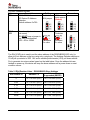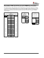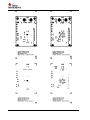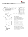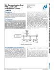
1
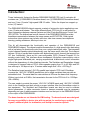
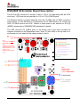
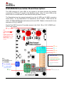
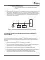
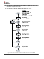
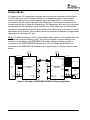
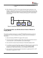
User’s Guide
SNLU100 – April 2012
SERDESUB-16USB User’s Guide
Table of Contents
TABLE OF CONTENTS..................................................................................................................................... 1
INTRODUCTION:............................................................................................................................................... 2
CONTENTS OF THE DEMO EVALUATION KIT: ............................................................................................. 3
DS90UB901Q/902Q SERDES TYPICAL APPLICATION: ............................................................................... 3
HOW TO SET UP THE DEMO EVALUATION KIT: .......................................................................................... 5
BI-DIRECTIONAL CONTROL BUS AND I2C MODES: ................................................................................... 6
DEMO BOARD POWER CONNECTIONS:....................................................................................................... 6
DS9UB901Q SERIALIZER BOARD DESCRIPTION:....................................................................................... 7
CONFIGURATION SETTINGS FOR THE SERIALIZER DEMO BOARD ......................................................................... 8
SERIALIZER LVCMOS AND FPD-LINK III PINOUT BY CONNECTOR .................................................................... 12
DS9UB902Q DESERIALIZER BOARD DESCRIPTION:................................................................................ 13
CONFIGURATION SETTINGS FOR THE DESERIALIZER DEMO BOARD ................................................................... 14
DESERIALIZER FPD-LINK III PINOUT AND LVCMOS BY CONNECTOR ................................................................ 18
TYPICAL CONNECTION AND TEST EQUIPMENT ....................................................................................... 19
EVALUATION OF THE BI-DIRECTIONAL CONTROL CHANNEL................................................................ 20
CAMERA MODE: ............................................................................................................................................. 20
I2C COMMUNICATION OVER BI-DIRECTIONAL CONTROL CHANNEL IN CAMERA MODE .......................................... 22
DISPLAY MODE: ............................................................................................................................................. 24
I2C COMMUNICATION OVER BI-DIRECTIONAL CONTROL CHANNEL IN DISPLAY MODE .......................................... 26
TROUBLESHOOTING DEMO SETUP............................................................................................................ 28
APPENDIX ....................................................................................................................................................... 30
SERIALIZER AND DESERIALIZER DEMO PCB SCHEMATICS: ............................................................................... 30
BOM (BILL OF MATERIALS) SERIALIZER DEMO PCB: ....................................................................................... 39
BOM (BILL OF MATERIALS) DESERIALIZER DEMO PCB: ................................................................................... 40
SERIALIZER (TX) DEMO PCB LAYOUT: ............................................................................................................ 41
SERIALIZER (TX) DEMO PCB STACKUP: .......................................................................................................... 44
DESERIALIZER (RX) DEMO PCB LAYOUT: ........................................................................................................ 45
DESERIALIZER (RX) DEMO PCB STACKUP:...................................................................................................... 48
SNLU100 – April 2012
SERDESUB-16USB User’s Guide
1
Introduction:
Texas Instruments’ Automotive Serdes DS90UB901Q/902Q FPD-Link III evaluation kit
contains one (1) DS90UB901Q Serializer board, one (1) DS90UB902Q Deserializer board,
and one (1) two (2) meter* high speed USB 2.0 cable. *Note: the chipset can support up
to ten (10) meters.
The DS90UB901Q/902Q chipset supports a variety of automotive vision applications over
a two (2) wire serial stream. The single differential pair (FPD-Link III) is well-suited for
direct connections between camera systems and Host Controller/Electronic Control Unit
(ECU)/FPGA. The bidirectional control channel of the DS90UB901Q/902Q provides
seamless communication between the image sensor and ECU/FPGA. Other typical
automotive vision systems may include: rear view, side view camera, lane departure
warning, parking assistance, blind spot view, etc.
This kit will demonstrate the functionality and operation of the DS90UB901Q and
DS90UB902Q chipset. The chipset enables transmission of a high-speed video data along
with a low latency bi-directional control bus over a single twisted pair cable. The integrated
control channel transfers data bi-directionally over the same serial video link. The transport
delivers 16 bits of parallel data together with bidirectional control channel that supports an
I2C bus. Additionally, there are six user-configurable GPIO (General Purpose IO) for
sending control data. This interface allows transparent full-duplex communication over a
single high-speed differential pair, carrying asymmetrical bi-directional control information
without the dependency of video blanking intervals. The Serializer and Deserializer chipset
is designed to transmit data at PCLK clocks speeds ranging from 10 to 43 MHz and I2C
bus rates up to 100 kbps at up to 10 meters cable length over -40 to +105 Deg C.
The Serializer board accepts 1.8V/3.3V parallel input signals. FPD-Link III Serializer
converts the 1.8V/3.3V LVCMOS parallel lines into a single serialized data pair with an
embedded clock. The serial data line rate switches at 28 times the base clock frequency.
With an input clock at 43 MHz, the transmission line rate for the FPD-Link III is 1.20Gbps
(28 x 43MHz).
The user needs to provide the proper 1.8V/3.3V LVCMOS inputs and 1.8V/3.3V LVCMOS
clock to the Serializer and also provide a proper interface from the Deserializer output to
test equipment. The Serializer and Deserializer boards can also be used to evaluate
device parameters. A cable conversion board or harness scramble may be necessary
depending on type of cable/connector interface used on the input to the DS90UB901Q and
to the output of the DS90UB902Q.
The demo boards are not intended for EMI testing. The demo boards were designed
for easy accessibility to device pins with tap points for monitoring or applying
signals, additional pads for termination, and multiple connector options.
2
SERDESUB-16USB User’s Guide
SNLU100 – April 2012
System Requirements:
In order to demonstrate, the following are required:
1) Video source with 1.8V or 3.3V LVCMOS parallel interface
2) Microcontroller (MCU) or FPGA with I2C interface bus (I2C master)
a. slave clock stretching must be supported by the I2C master controller/MCU.
3) External peripheral device that supports I2C (slave mode)
4) Power supply for 1.8V (required) and 3.3V (optional)
Contents of the Demo Evaluation Kit:
1)
2)
3)
4)
5)
One Serializer board with the DS90UB901Q
One Deserializer board with the DS90UB902Q
One 2-meter high speed USB 2.0 cable (4-pin USB A to 5-pin mini USB)
Evaluation Kit Documentation (this manual)
DS90UB901Q/902Q Datasheet
DS90UB901Q/902Q Serdes Typical Application:
Camera Module
Video Data
Image
Sensor
HSYNC
VSYNC
Pixel Clock
DOUT+
Video Data
RIN+
ROUT
[13:0]
HS,VS
DIN[13:0]
HS,VS
DOUTPCLK
RIN-
PCLK
FPD-Link III
GPIO
SDA
SCL
Bidirectional
Control Bus
Pixel Clock
MCU / FPGA
GPIO
GPIO[1:0]
I2C CNTL
HSYNC
VSYNC
GPIO[1:0]
SDA
SDA
SCL
SCL
DS90UB901Q
Serializer
DS90UB902Q
Deserializer
SDA
I2C CNTL
SCL
Bidrectional
Control Bus
Figure 1. Typical Application
The diagram above illustrates a typical application of DS90UB901Q/902Q chipset. The
MCU/FPGA can program device registers on the DS90UB901Q, DS90UB902Q, and
remote peripheral device, such as a camera.
SNLU100 – April 2012
SERDESUB-16USB User’s Guide
3
Camera Module
(Video Data + Ctrl)
DS90UB901Q
Serializer
(I2C_CTRL)
FPD-LINK III
DS90UB902Q
Deserializer
(I2C_CTRL)
(Video Data + Ctrl)
Host Controller /
FPGA /
Video Processor
LCD
Display
Figure 2. Typical DS90UB901Q/902Q Camera System Diagram
Figure 1 and Figure 2 illustrate the use of the Chipset (Serializer/Deserializer) in a
Camera to Host (MCU/FPGA) Controller.
Refer to the proper datasheet information on Chipsets (Serializer/Deserializer) provided on
each board for more detailed information.
4
SERDESUB-16USB User’s Guide
SNLU100 – April 2012
How to set up the Demo Evaluation Kit:
The DS90UB901Q/902Q evaluation boards consist of two sections. The first part of the
board provides the point-to-point interface for transmitting parallel video data. The second
part of the board allows bi-directional control communication of an I2C bus control of using
a MCU/FPGA to programming a remote peripheral device via the Deserailizer.
The PCB routing for the Serializer input pins (DIN) accept incoming parallel video data at
1.8V/3.3V LVCMOS signals from J1 IDC connector. The FPD-Link III interface uses a
single twisted pair cable (provided). The output pins (ROUT) are accessed through a J7
IDC connector. Please follow these steps to set up the evaluation kit for bench testing and
performance measurements:
1) A two (2) meter high speed USB 2.0 cable has been included in the kit. Connect the 41
2
3
4
A
pin USB A
side of cable harness to the serializer board and the other
side of the harness, the 5-pin mini USB jack 1 2 3 4 MINI to the Deserializer board.
This completes the FPD-Link III interface connection.
NOTE: The DS9UB901Q and DS9UB902Q are NOT USB compliant and should
not be plugged into a USB device nor should a USB device be plugged into the
demo boards.
2) Jumpers and switches have been configured at the factory; they should not require any
changes for immediate operation of the chipset. See text on Configuration settings
and datasheet for more details.
3) From the video source, connect a flat cable (not supplied) to the Serializer board and
connect another flat cable (not supplied) from the Deserializer board to the controller.
Note: For 50 ohm signal sources, provide 1.8V/3.3V LVCMOS input signal levels into
DIN[13:0],HS,VS and PCLK and add 50 ohm parallel termination resistors R3-R19 on
the DS9UB901Q Serializer board.
4) Connect the Serializer I2C ports to the I2C of the peripheral slave device. Connect the
Deserializer I2C ports to the I2C bus of the MCU/FPGA (I2C master).
5) Power for the Serializer and Deserializer boards must be supplied externally through
Power Jack (VDD). Grounds for both boards are connected through Power Jack (VSS)
(see section below).
SNLU100 – April 2012
SERDESUB-16USB User’s Guide
5
Bi-Directional Control Bus And I2C Modes:
In order to communicate and synchronize with remote devices on the I2C bus through the
bi-directional control channel, slave clock stretching must be supported by the I2C master
controller/MCU. The chipset utilizes bus clock stretching (holding the SCL line low) during
data transmission; where the I2C slave pulls the SCL line low prior to the 9th clock of
every I2C data transfer (before the ACK signal).
The bidirectional control bus supports is a I2C compatible interface that allows
programming of the DS90UB901Q, DS90UB902Q, or an external remote device (such as
a camera or display). Register programming transactions to/from the DS90UB901Q/902Q
chipset are employed through the clock (SCL) and data (SDA) lines. These two signals
have open drain I/Os and must be pulled-up to VDDIO by external resistors. The boards
have an option to use the on-board 1.0KΩ pull-up resistors tied to VDDIO or connected
through external pull-ups at the target Host. The appropriate pull-up resistor values will
depend upon the total bus capacitance and operating speed. The DS90UB901Q/902Q I2C
bus data rate supports up to 100 kbps according to I2C specification.
To start any data transfer, the DS90UB901Q/902Q must be configured in the proper I2C
mode. Each device can function as an I2C slave proxy or master proxy depending on the
mode determined by MODE (M_S) pin. Note the MODE pin is label as M_S on the PCB
boards. The Ser/Des interface acts as a virtual bridge between Master controller (MCU)
and the remote device. When the MODE (M_S) pin is set to High, the device is treated as
a slave proxy; acts as a slave on behalf of the remote slave. When addressing a remote
peripheral or Serializer/Deserializer (not wired directly to the MCU), the slave proxy will
forward any byte transactions sent by the Master controller to the target device. When
MODE (M_S) pin is set to Low, the device will function as a master proxy device; acts as a
master on behalf of the I2C master controller. Note that the devices must have
complementary settings for the MODE configuration. For example, if the Serializer MODE
(M_S) pin is set to High then the Deserializer MODE (M_S) pin must be set to Low and
vice-versa.
Demo Board Power Connections:
The Serializer and Deserializer boards must be powered by supplying power externally
through J3 (VDD) and J4 (VSS) on Serializer Board and J4 (VDD) and J5 (VSS) on
Deserializer board. Note +2.5V is the MAXIMUM voltage that should ever be applied to
the Serializer J3 or Deserializer J4 VDD terminal. Serializer JP1 VDDI and Deserializer
VDDIO JP1 must never exceed +4.0V. Damage to the device(s) can result if the voltage
maximum is exceeded.
6
SERDESUB-16USB User’s Guide
SNLU100 – April 2012
DS9UB901Q Serializer Board Description:
The 2x17-pin IDC connector J1 accepts 16 bits of 1.8V or 3.3V data along with the PCLK
clock input. VDDI must be set externally for 1.8V or 3.3V LVCMOS inputs.
The Serializer board is powered externally from the J3 (VDD) and J4 (VSS) connectors
shown below. For the Serializer to be operational, the S1-PDB switch on S1 must be set
HIGH. S1-RES0 must be set LOW. Master or slave mode is user selected on S1-M_S
(MODE); please refer to DS90UB901/902 datasheet for details.
The USB connector P3 (USB-A side) on the bottom side of the board provides the
interface connection to the Deserializer board. Note: P2 (mini USB) on the top side is unstuffed and not to be used with the cable provided in the kit.
f J3, J4
JP1
Note:
1) VDD and VSS MUST be
applied externally from
here.
2) VDDI = 3.3V should be
applied separately on JP1
with default jumper on JP2
(VDDI=+3.3V),
otherwise jumper VDDI to
+1.8V
c FPD-Link III I/O
d LVCMOS INPUTS
e FUNCTION CONTROLS
f POWER SUPPLY
1.8V
g INPUT TERMINATION
(For 50Ω signal sources,
add 50Ω termination, otherwise
leave unpopulated)
h I2C BUS CONTROL
i GPIO
J1
i
J1
d
g
g
S1
g
Note:
Connect cable
(USB A side)
to P2 on BACKSIDE.
c P3 (BACKSIDE)
c P2 (TOPSIDE)
e
J6,JP8
g
(UNSTUFFED)
h
SNLU100 – April 2012
SERDESUB-16USB User’s Guide
7
Configuration Settings for the Serializer Demo Board
VDDI: 1.8V or 3.3V LVCMOS INPUT/OUTPUT SELECTION
Reference
Description
+1.8V VDDI
+3.3V VDDI
VDDI LVCMOS
VDDI = 3.3V
JP2
VDDI = 1.8V
I/O level configuration.
(Default)
JP1
NOT USED
1.8V
1.8V
LVCMOS
inputs
JP2
1.8V
apply external
3.3V
LVCMOS
inputs
S1: Serializer Input Features Selection
Reference
Description
Input = L
Input = H
M_S
Master
Slave
2
I C Master / Slave
(MODE)
(Default)
select
PDB
PowerDown Bar
Powers
Operational
Down
(Default)
RES 0
Reserved
MUST be
(* IMPORTANT
tied low for
See user note
normal
below)
operation
(Default)
S1
*Note:
In user layout RES 0 (pin 7) MUST be tied low for proper operation.
8
SERDESUB-16USB User’s Guide
SNLU100 – April 2012
JP4,VR3: Address Decoder
Reference
Description
DS90UB901Q
JP4
I2C Device ID Address
Selection
Default address: 0xB0’h
JP4 &
VR3
RID value adjustment
(via screw)
JP4 MUST have a jumper to
use VR3 potentiometer.
VR3 = 0Ω to 100KΩ
Setting
Enabled –
With jumper
Connector
VSS –
Default address
(Default)
Clockwise
CounterClockwise
Decreases
RID value
Increases
RID value
The ID[x] (CAD) pin is used to set the physical slave address of the DS90UB901Q (I2C
only) to allow up to six devices on the bus using only a single pin. The Address Decoder
employs a 10 kΩ pull up resistor to +1.8V and a variable potentiometer (VR3) for the pull
down resistor RID to GND to generate six unique values based on the table below. Once
the address bits are latched on power up, the device will keep the slave address until a
power down or reset condition occurs.
Figure 3. ID[x] Pin Connection Diagram
SNLU100 – April 2012
SERDESUB-16USB User’s Guide
9
Table 1. ID[x] Resistor Value – DS90UB901Q Slave Address
Address 8'b
Rid Resistor Ω
Address 7'b
0 appended (WRITE)
0
7b' 101 1000 (h'58)
8b' 1011 0000 (h'B0)
2.0K
7b' 101 1001 (h'59)
8b' 1011 0010 (h'B2)
4.7K
7b' 101 1010 (h'5A)
8b' 1011 0100 (h'B4)
8.2K
7b' 101 1011 (h'5B)
8b' 1011 0110 (h'B6)
12.1K
7b' 101 1100 (h'5C)
8b' 1011 1000 (h'B8)
39.0K
7b' 101 1110 (h'5E)
8b' 1011 1100 (h'BC)
Serializer Bidirectional Control Bus (SCL, SDA) – I2C Compliant
Reference
Description Settings
J6
Pinout:
I2C Port
1 – VDD_I2C
2 – SCL
3 – SDA
4 – VSS
JP8
10
I2C Input
Port
SERDESUB-16USB User’s Guide
Closed:
VDD_I2C power is
applied through the
VDDIO source with
onboard 1.0Kohm
pull up resistors
(Default)
Connector
Open:
VDD_I2C power is
applied externally
Note: when
connecting the bus
externally, the
target source must
have external pull
up resistor.
SNLU100 – April 2012
JP6, JP7: USB Red and Black wire
Reference
Description
Power wire in USB cable
JP6
thru P3 (and P2 not
mounted) connector
Jumper RED to VSS –
recommended
VDD
VSS
Red wire tied Red wire
tied to VSS
to VDD
(Default)
OPEN
Red wire
floating
(not
recommended)
JP6
JP6
JP6
Black wire
tied to VDD
Black wire
tied to VSS
(Default)
Black wire
floating
(not
recommended)
JP7
JP7
JP7
Note: Normally VDD in USB application
Power wire in USB cable
thru P3 (and P2 not
mounted) connector
Jumper BLACK to VSS –
recommended
JP7
Note: Normally VSS in USB application
top side thru the board view
(mounted on solder side)
P2
pin 3
pin 4
BLACK WIRE
pin 2
+
_
pin 1
RED WIRE
USB A
SNLU100 – April 2012
SERDESUB-16USB User’s Guide
11
Serializer LVCMOS and FPD-Link III Pinout by Connector
The following three tables illustrate how the Serializer connections mapped to the IDC
connector J1, the FPD-Link III I/O on the USB-A connector P3, and the mini USB P2 (not
mounted) pinouts. Note – labels are also printed on the demo boards for both the
LVCMOS inputs/outputs and FPD-Link III I/Os.
J1
LVCMOS I/O
pin no.
name
name
pin no.
1
GND
GPIO[0]
2
3
GND
GPIO[1]
5
7
9
11
13
15
17
19
21
23
25
27
29
31
33
35
GND
DIN0
GND
DIN1
GND
DIN2
GND
DIN3
GND
DIN4
GND
DIN5
GND
DIN6
GND
DIN7
GND
DIN8
37
12
P2
(topside)
FPD-Link III
(not mounted)
pin no.
name
4
1
JP6
pin no.
name
2
3
4
DOUT+
DOUTJP7
5
4
3
2
1
JP6
NC
DOUTDOUT+
JP7
GND
DIN9
GND
DIN10
GND
DIN11
GND
DIN12
GND
DIN13
GND
HS
GND
VS
6
8
10
12
14
16
18
20
22
24
26
28
30
32
34
36
GND
PCLK
38
SERDESUB-16USB User’s Guide
P3
(bottom side)
FPD-Link III
SNLU100 – April 2012
DS9UB902Q Deserializer Board Description:
The USB connector J2 (mini USB) on the topside of the board provides the interface
connection for FPD-Link III signals to the Serializer board. Note: J11 (mini USB) on the
bottom side is un-stuffed and not used with the cable provided in the kit.
The Deserializer board is powered externally from the J4 (VDD) and J5 (VSS) connectors
shown below. For the Deserializer to be operational, the S1 switch – PDB must be set
HIGH. S1-RES0, BISTEN (Normal mode) must be set LOW. Master or slave mode is user
selected on S1-M_S (MODE)..
The 2x17 pin IDC Connector J7 provides access to the 16 bit 1.8V or 3.3V LVCMOS and
PCLK clock outputs.
f J4, J5, JP1
Note:
1) VDD and VSS MUST be
applied externally from
here.
2) VDDI = 3.3V should be
applied separately on JP1
with default jumper on JP2
(VDDI=+3.3V),
otherwise jumper VDDIO
to +1.8V
1.8V
d JP4
h J7
d JP5
d P1
Note:
Connect cable
(mini USB side) to J2
on (TOPSIDE).
c J2 (TOPSIDE)
c J11 (BACKSIDE)
c FPD-Link III I/O
d LVCMOS OUTPUTS
e FUNCTION CONTROLS
f POWER SUPPLY
g I2C BUS CONTROL
h GPIO
(UNSTUFFED)
g JP8, JP9, J8
e S1
SNLU100 – April 2012
SERDESUB-16USB User’s Guide
13
Configuration Settings for the Deserializer Demo Board
VDDIO: 1.8V or 3.3V LVCMOS INPUT/OUTPUT SELECTION
Reference
Description
+1.8V VDDIO +3.3V VDDIO
VDDIO LVCMOS
JP2
VDDIO = 1.8V VDDIO = 3.3V
I/O level configuration.
(Default)
1.8V
1.8V
1.8V
LVCMOS
S1: Deserializer Input Features Selection
Reference
Description
Input = L
PDB
PowerDown Bar
Power
Down
(Disabled)
BISTEN
BIST Enable Pin
Normal
operating
mode.
BIST is
disabled.
(Default)
M_S
Master
2
I C Master / Slave
(MODE)
select
Reserved
MUST be
RES 0
(* IMPORTANT
tied low for
See user note
normal
below)
operation
(Default)
JP2
apply external
3.3V
LVCMOS
Input = H
Operational
(Default)
S1
BIST Mode is
enabled.
Slave
(Default)
*Note: In user layout RES 0 (pin 39) MUST be tied low for proper operation.
14
SERDESUB-16USB User’s Guide
SNLU100 – April 2012
JP8,VR3: Address Decoder
Reference
Description
DS90UB902Q
JP8
I2C Device ID Address
Selection
Default address: 0xC0’h
RID value adjustment
(via screw)
JP8 MUST have a jumper to
use VR3 potentiometer.
VR3 = 0Ω to 100KΩ
JP8 &
VR3
Setting
Enabled –
With jumper
Connector
VSS –
Default address
(Default)
Clockwise
CounterClockwise
Decreases
RID value
Increases
RID value
The ID[x] (CAD) pin is used to set the slave address of the DS90UB902Q (I2C only) to
allow up to six devices on the bus using only a single pin. The Address Decoder employs a
10 kΩ pull up resistor to VDD 1.8V and a variable potentiometer (VR3) pull down resistor
RID to generate six unique values based on the table below. Once the address bits are
latched on power up, the device will keep the slave address until a power down or reset
condition occurs.
Table 2. ID[x] Resistor Value – DS90UB902Q Slave Address
Address 8'b
Rid Resistor Ω
Address 7'b
0 appended (WRITE)
0
7b' 110 0000 (h'60)
8b' 1100 0000 (h'C0)
2.0K
7b' 110 0001 (h'61)
8b' 1100 0010 (h'C2)
4.7K
7b' 110 0010 (h'62)
8b' 1100 0100 (h'C4)
8.2K
7b' 110 0011 (h'62)
8b' 1101 0110 (h'C6)
12.1K
7b' 110 0100 (h'62)
8b' 1101 1000 (h'C8)
39.0K
7b' 110 0110 (h'66)
8b' 1100 1100 (h'CC)
SNLU100 – April 2012
SERDESUB-16USB User’s Guide
15
Deserializer Bidirectional Control Bus (SCL, SDA) - I2C Compliant
Reference
Description Settings
J8
Pinout:
I2C Port
1 – VDD_I2C
2 – SCL
3 – SDA
4 – VSS
JP9
16
I2C Input
Port
SERDESUB-16USB User’s Guide
Closed:
VDD_I2C power is
applied through the
VDDIO source with
onboard 1.0Kohm
pull up resistors
(Default)
Connector
Open:
VDD_I2C power is
applied externally
Note: when
connecting the bus
externally, the
target source must
have external pull
up resistor.
SNLU100 – April 2012
JP5: Output Lock Monitor
Reference
Description
LOCK
Receiver PLL LOCK
Note:
DO NOT SHORT
JUMPER IN JP5.
JP4: Output Pass Monitor
Reference
Description
PASS
PASS (CRC / BIST modes)
Note:
DO NOT SHORT
JUMPER IN JP4.
JP6, JP7: USB Red and Black wire
Reference
Description
Power wire in USB cable
JP6
thru J2 (and J11 not
mounted) connector
Jumper RED to VSS –
recommended
Output = L
Unlocked
Output = H
Locked
JP5
Output = L
ERROR
Output = H
PASS
JP4
VDD
VSS
Red wire tied Red wire
to VDD
tied to VSS
(Default)
JP6
JP6
OPEN
Red wire
floating
(not
recommended)
JP6
Note: Normally VDD in USB application
JP7
Power wire in USB cable
thru J2 (and J11 not
mounted) connector
Jumper BLACK to VSS –
recommended
Black wire
tied to VDD
Black wire
tied to VSS
(Default)
Black wire
floating
(not
recommended)
JP7
JP7
JP7
Note: Normally VSS in USB application
mini USB
J2
pin 1
RED WIRE
pin 2
+
_
pin 3
NO connect
pin 4
pin 5
top side view
(mounted on component side)
SNLU100 – April 2012
BLACK WIRE
SERDESUB-16USB User’s Guide
17
Deserializer FPD-Link III Pinout and LVCMOS by Connector
The following three tables illustrate how the Deserializer connections mapped to the IDC
connector J7, the mini USB connector J2, and the mini USB connector J11 pinouts. Note –
labels are also printed on the demo boards for both the FPD-Link III I/O and LVCMOS
inputs/outputs.
J7
pin no.
18
LVCMOS I/O
name
name
pin no.
J2
(topside)
FPD-Link III
J11
(bottom side)
(not mounted)
1
GPIO[0]
GND
2
pin no.
name
3
GPIO[1]
GND
4
1
JP6
pin no.
name
5
7
9
11
13
15
17
19
21
23
25
27
29
31
33
35
37
ROUT0
GND
ROUT1
GND
ROUT2
GND
ROUT3
GND
2
3
4
5
RIN+
RINNC
JP7
5
4
3
2
ROUT4
GND
JP6
NC
RINRIN+
JP7
ROUT5
GND
ROUT6
GND
ROUT7
GND
ROUT8
GND
ROUT9
GND
ROUT10
GND
ROUT11
GND
ROUT12
GND
6
8
10
12
14
16
18
20
22
24
26
28
30
32
34
36
38
ROUT13
GND
HS
GND
VS
GND
PCLK
GND
SERDESUB-16USB User’s Guide
FPD-Link III
1
SNLU100 – April 2012
Typical Connection and Test Equipment
The following is a list of typical test equipment that may be used to generate signals for the
Serializer inputs:
1) Digital Video Source – for generation of specific display timing such as CMOS imager
or Graphics Controller with digital video signals (1.8V/3.3V LVCMOS).
2) Any other signal generator / video source that generates the correct input levels.
The following is a list of typical test equipment that may be used to monitor the output
signals from the Deserializer:
1) Controller or capture card which supports digital video signals (1.8V/3.3V
LVCMOS).
2) Video capture card
3) Microcontroller or FPGA with an I2C interface
4) Optional – Logic Analyzer or Oscilloscope
5) Any SCOPE with a bandwidth of at least 50MHz for 1.8V/3.3V LVCMOS and/or
1.5GHz for observing differential signals.
Figure 4 below illustrates an application using a camera connected to DS90UB901Q with
I2C bus and a MCU/FPGA controller connected to DS90UB902Q with I2C bus. Both
Camera video and control information are transferred on the same serial video link.
SNLU100 – April 2012
SERDESUB-16USB User’s Guide
19
Evaluation of the Bi-directional Control Channel
VDDIO
VDD18
VDDIO
VDD18
This section describes how to perform I2C instructions between MCU/FPGA and a remote
peripheral device through the DS90UB902Q and DS90UB901Q pair configured in a
camera type of application. Figure 4 shows the configuration of evaluation boards for I2C
communication. A MCU/FPGA controller with an I2C interface is required. Refer to the
DS90UB901Q/902Q datasheet for the definition of each register.
SCL
SDA
Figure 4. Example of DS90UB901Q/902Q in Camera Application
Camera Mode:
In Camera mode, I2C transactions originate from the Master controller at the Deserializer
side (Figure 4). The I2C slave core in the Deserializer will detect if a transaction is
intended for the Serializer or a slave at the Serializer. Commands are sent over the bidirectional control channel to initiate the transactions. The Serializer will receive the
command and generate an I2C transaction on its local I2C bus. At the same time, the
Serializer will capture the response on the I2C bus and return the response on the forward
channel link. The Deserializer parses the response and passes the appropriate response
to the Deserializer I2C bus.
20
SERDESUB-16USB User’s Guide
SNLU100 – April 2012
Procedure - Camera Mode:
1) Connect the 1.8V and 3.3V power with +1.8V and +3.3V supplies accordingly. Keep
the power off.
2) Verify that all the jumper positions and switches are correctly set (as per default
positions defined in “Configuration Settings for the Serializer/Deserializer Demo
Board” tables).
3) Connect the USB interface cable between P3 (DS90UB901Q board) connector and
J2 connector (DS90UB902Q board). Note that hot-plugging assertion of cable
between Serializer and Deserializer is not supported.
4) Set hardware configuration for DS90UB901Q Serializer and DS90UB902Q
Deserializer devices
a. Verify peripheral device (camera) address is set to 0xA0
b. Set to Camera mode: Serializer MODE (M_S) pin = L and Deserializer
MODE (M_S) pin = H
c. Set Serializer and Deserializer I2C slave address on ID[x] (CAD) pin:
i. Serializer Rid=0ohm; Serializer I2C slave address is 0xB0
ii. Deserializer Rid=0ohm; Deserializer I2C slave address is 0xC0
5) Turn on the +1.8V and +3.3V power supplies
6) The DS90UB902Q Deserializer I2C slave is enabled to receive data directly from
the I2C Master Controller. I2C transfers are processed in a one byte basis. After
receiving one byte, the Deserializer slave will need to acknowledge (ACK) the
transfer to receive the next following byte. The Deserializer slave holds SCL low
(clock stretch) for the required period until an ACK (or NACK) is established and
then releases it. The Deserializer I2C slave acknowledges all the transfers
addressed to Deserializer, Serializer, or remote device.
7) Before initiating any I2C commands, the Deserializer needs to be programmed with
the target slave device addresses and Serializer device address. SER_DEV_ID
Register 0x07h sets the Serializer device address and SLAVE_x_MATCH/
SLAVE_x_INDEX registers 0x08h~0x17h set the remote target slave addresses. In
slave mode the address register is compared with the address byte sent by the I2C
master. If the addresses are equal to any of registers values, the I2C slave will
acknowledge and hold the bus to propagate the transaction to the target device
otherwise it returns no acknowledge.
8) Execute I2C instructions to write the following registers
a. Assign ID Match values for camera address on Deserializer
i. Write 0xA0 to Register 0x08 of Deserializer (0xC0)
ii. Write 0xA0 to Register 0x10 of Deserializer (0xC0)
SNLU100 – April 2012
SERDESUB-16USB User’s Guide
21
b. DS90UB902Q Deserializer (0xC0)
i. Write 0x04 to Register 0x01
1. Verify that LOCK LED2 is lit; This indicates the chipset is
Locked
9) After initialization, the camera PCLK clock and input data can begin transmission to
the Serializer. The Serializer locks onto PCLK input (if present) otherwise the onchip oscillator (25 MHz) is used as the input clock source. Note the MCU controller
should monitor the LOCK pin and confirm LOCK = H before performing any I2C
communication across the link.
Figure 5. Virtual device addressing from MCU/FPGA I2C controller
I2C Communication over Bi-directional Control Channel in
Camera Mode
This section provides instructions for a simple I2C Read/Write transaction over the bidirectional control channel validating the interface between the host and Deserializer to
Serializer.
1) Check the Deserializer SER DEV ID register 0x07 contents
2) The value entered in Deserializer register 0x07 sets the target Serializer device to
communicate with. Load the Serializer slave address register.
3) Host controller to load and transmit data byte to Serializer address 0xB0
4) For verification purposes Serializer register 0x13 General-purpose register will be
exercised for reading and writing data. Other Serializer registers can be
programmed to check internal functions; such as register 0x03 b[0] TRFB.
22
SERDESUB-16USB User’s Guide
SNLU100 – April 2012
5) Host controller to load and transmit write transaction to register byte 0x13 = 0xFF.
Note default of register 0x13 = 0x00.
6) Host controller to read back Serializer 0xB0 register 0x13 = 0xFF
Figure 6. Bi-directional Control Channel Flowchart in Camera Mode
SNLU100 – April 2012
SERDESUB-16USB User’s Guide
23
Display Mode:
In Display mode, I2C transactions originate from the controller attached to the Serializer.
The I2C slave core in the Serializer will detect if a transaction targets (local) registers
within the Serialier or the (remote) registers within the Deserializer or a remote slave
connected to the I2C master interface of the Deserializer. Commands are sent over the
forward channel link to initiate the transactions. The Deserializer will receive the command
and generate an I2C transaction on its local I2C bus. At the same time, the Deserializer
will capture the response on the I2C bus and return the response as a command on the bidirectional control channel. The Serializer parses the response and passes the appropriate
response to the Serializer I2C bus.
Note: The default settings for this EVK are shipped with a camera mode configuration, but
this EVK also supports a display mode. This mode is suitable for setups where a host
controller is connected to the DS90UB901Q Serializer end and a display module is
connected to the DS90UB902Q Deserializer end. The I2C Master would need to be
connected to the DS90UB901Q Serializer end. A typical setup for display mode is shown
below:
DOUT
+
-
-
PCLK
GPIO0
GPIO1
GPU/FPGA
Host
VDDIO
DS90UB901Q
Serializer
10k
1.0k
SCL
SDA
Timing Controller
1.8V
DS90UB902Q
Deserializer
10k
ID[x]
0
ROUT[13:0]
HS,VS
PCLK
PDB
ID[x]
VDDIO
RIN
(3.3V I/O)
VDDIO
PDB
1.8V
VDDIO
+
VDD18
DIN[13:0]
HS,VS
1.8V 3.3V
VDDIO
(3.3V I/O)
VDD18
1.8V 3.3V
PASS
LOCK
GPIO0
GPIO1
0
VDDIO
VDDIO
1.0k
SCL
SDA
MODE (M_S)
RES0
0xB0
1.0k
MODE (M_S)
BISTEN, RES0
LCD
Display
1.0k
SCL
SDA
C
0xA0
0xC0
Figure 7. Example of DS90UB901Q/902Q in Display Application
24
SERDESUB-16USB User’s Guide
SNLU100 – April 2012
Procedure - Display Mode:
1) Connect the 1.8V and 3.3V power with +1.8V and +3.3V supplies accordingly. Keep
the power off.
2) Verify that all the jumper positions and switches are correctly set.
NOTE: For Display Mode, the default settings for switch S1-M_S on S1 for the
DS90UB901Q Serializer and DS90UB902Q Deserializer boards must be reversed.
DS90UB901Q board: S1
DS90UB902Q board: S1
3) Connect the USB interface cable between P3 (DS90UB901Q board) connector and
J2 connector (DS90UB902Q board).
4) Set hardware configuration for DS90UB901Q Serializer and DS90UB902Q
Deserializer devices
a. Peripheral device (display) address is set to 0xA0
b. Set to Display mode: Serializer MODE (M_S) pin = H and Deserializer
MODE (M_S) pin = L
c. Set Serializer and Deserializer I2C slave address on ID[x] (CAD) pin:
i. Serializer Rid=0ohm; Serializer I2C slave address is 0xB0
ii. Deserializer Rid=0ohm; Deserializer I2C slave address is 0xC0
5) Turn on the +1.8V and +3.3V power supplies
6) Before initiating any I2C commands, the Serializer needs to be programmed with
the target slave device address and Deserializer device address. DES_DEV_ID
Register 0x06h sets the Deserializer device address and SLAVE_DEV_ID register
0x7h sets the remote target slave address. If the I2C slave address matches any of
registers values, the I2C slave will hold the transaction allowing read or write to
target device. Note: In Display mode operation, registers 0x08h~0x17h on
Deserializer must be reset to 0x00.
7) Execute I2C instructions to write the following registers
a. DS90UB901Q Serializer (0xB0)
b. Set target slave device address on the Serializer
i. Write 0xA0 to Register 0x07 of Serializer (0xB0)
SNLU100 – April 2012
SERDESUB-16USB User’s Guide
25
1. Verify that LOCK LED2 is lit; This indicates the chipset is
Locked
8) After initialization, the PCLK clock and input data can begin transmission to the
Serializer. The Serializer locks onto PCLK input (if present) otherwise the on-chip
oscillator (25 MHz) is used as the input clock source. Note the user should monitor
the LOCK pin and confirm LOCK = H before performing any I2C communication
across the link.
Figure 8. Virtual device addressing from GPU/FPGA I2C controller
I2C Communication over Bi-directional Control Channel in
Display Mode
This section provides instructions for a simple I2C Read/Write transaction over the bidirectional control channel validating the interface between the host and Serializer to
Deserializer.
1) Check the Serializer DES DEV ID register 0x06 contents
2) The value entered in Serializer register 0x06 sets the target Deserializer device to
communicate with. Load the Deserializer slave address register.
3) Host controller to load and transmit data byte to Deserializer address 0xC0
4) For verification purposes Deserializer register 0x13 General-purpose register will be
exercised for reading and writing data. Other Deserializer registers can be
programmed to check internal functions; such as register 0x03 b[0] RRFB.
5) Host controller to load and transmit write transaction to register byte 0x13 = 0xFF.
Note default of register 0x13 = 0x00.
26
SERDESUB-16USB User’s Guide
SNLU100 – April 2012
6) Host controller to read back Deserializer 0xC0 register 0x13 = 0xFF
Configuration:
Serializer: ADDR = 0xB0h
Slave mode (MODE = H); PDB=H
START
Deserializer: ADDR: 0xC0h
Master mode (MODE = L); BISTEN=L, PDB=H
LOCK = H
Read data from
0xB0
Write/Verify 0xB0
Reg 0x06 = 0xC0
NO
Register 0x06
= 0xC0
Read Deserializer
Register 0x06 SER DEV ID
Write command to Deserializer
Reg 0x06 SER DEV ID
YES
Read data from
0xC0
NO
Register 0x13
= 0x00
Send Read command to
Serializer Reg 0x13 GPCR
Read Back Serializer
Reg 0x13 GPCR
YES
NO
Write to 0xC0
Reg 0x13 = 0xFF
Send Write command to
Serializer Reg 0x13 GPCR
Read data from
0xC0
Send Read command to
Serializer Reg 0x13 GPCR
Register 0x13
= 0xFF
YES
NO
Data received
match?
Read Back Serializer
Reg 0x13 GPCR
YES
END
Figure 9. Bi-directional Control Channel Communication Flowchart in Display Mode
SNLU100 – April 2012
SERDESUB-16USB User’s Guide
27
Troubleshooting Demo Setup
NOTE: The DS9UB901Q and DS9UB902Q are NOT USB compliant and should not be
plugged into a USB device nor should a USB device be plugged into the demo
boards.
If the demo boards are not performing properly, use the following as a guide for quick
solutions to potential problems. If the problem persists, please contact the local Sales
Representative for assistance.
QUICK CHECKS:
1. Check that Powers and Grounds are connected to both Serializer and Deserializer
boards.
2. Check the supply voltage (typical 1.8V) and also current draw with both Serializer and
Deserializer boards. The Serializer board should draw about 70mA with clock and all
data bits switching at 43 MHz. The Deserializer board should draw about 100mA with
clock and all data bits switching at 43 MHz.
3. Verify input clock and input data signals meet requirements (VIL, VIH, tset, thold), Also
verify that data is strobed on the selected rising/falling (RFB register) edge of the clock.
4. Check that the Jumpers and Switches are set correctly.
5. Check that the cable is properly connected.
TROUBLESHOOTING CHART
Problem…
There is only the output clock.
Solution…
Make sure the data is applied to the correct input pin.
There is no output data.
Make sure data is valid at the input.
No output data and clock.
Make sure Power is on. Input data and clock are
active and connected correctly.
Power, ground, input data and
input clock are connected
correctly, but no outputs.
Make sure that the cable is secured to both demo
boards.
Check the Power Down pins of both Serializer and
Deserializer boards to make sure that the devices are
enabled (PDB=Vdd) for operation.
The devices are pulling more
than 1A of current.
Check for shorts in the cables connecting the
Serializer and Deserializer boards.
After powering up the demo
boards, the power supply
reads less than 1.8V when it is
set to 1.8V.
Use a larger power supply that will provide enough
current for the demo boards, a 500mA minimum
power supply is recommended.
28
SERDESUB-16USB User’s Guide
SNLU100 – April 2012
Note: Please note that the following references are supplied only as a courtesy to our
valued customers. It is not intended to be an endorsement of any particular equipment or
supplier.
Cable References
The FPD-Link III interface cable included in the kit is a standard off-the-shelf high-speed
USB 2.0 with a 4-pin USB A type on one end and a 5-pin mini USB on the other end and is
included for demonstration purposes only.
NOTE: The DS9UB901Q and DS9UB902Q are NOT USB compliant and should not be
plugged into a USB device nor should a USB device be plugged into the demo
boards.
The inclusion of the USB cable in the kit is for:
1) Demonstrating the robustness of the FPD-Link III link over standard twisted pair data
cables.
2) Readily available and in different lengths without having custom cables made.
- For optimal performance, we recommend Shielded Twisted Pair (STP) 100ohm
differential impedance and 24 AWG (or larger diameter) cable for high-speed data
applications.
Leoni Dacar 538 series cable:
www.leoni-automotive-cables.com
Rosenberger HSD connector:
www.rosenberger.de/en/Products/35_Automotive_HSD.php
Equipment References
Corelis CAS-1000-I2C/E I2C Bus Analyzer and Exerciser Products:
www.corelis.com/products/I2C-Analyzer.htm
SNLU100 – April 2012
SERDESUB-16USB User’s Guide
29
Appendix
Serializer and Deserializer Demo PCB Schematics:
30
SERDESUB-16USB User’s Guide
SNLU100 – April 2012
SNLU100 – April 2012
SERDESUB-16USB User’s Guide
31
32
SERDESUB-16USB User’s Guide
SNLU100 – April 2012
SNLU100 – April 2012
SERDESUB-16USB User’s Guide
33
34
SERDESUB-16USB User’s Guide
SNLU100 – April 2012
SNLU100 – April 2012
SERDESUB-16USB User’s Guide
35
36
SERDESUB-16USB User’s Guide
SNLU100 – April 2012
SNLU100 – April 2012
SERDESUB-16USB User’s Guide
37
38
SERDESUB-16USB User’s Guide
SNLU100 – April 2012
BOM (Bill of Materials) Serializer Demo PCB:
DS90UB901 Tx Demo Board - Board Stackup Revised: Tuesday, July 27, 2010
DS90UB901 Tx Demo Board
Revision: 1B
Bill Of Materials
Item
Quantity Reference
Part
______________________________________________
1
2
3
4
5
6
7
8
9
10
11
12
13
14
15
16
17
18
19
20
21
22
2
2
4
2
6
2
6
5
2
3
5
1
1
1
2
1
1
2
1
1
1
18
23
24
25
26
27
28
29
30
31
32
33
34
35
36
37
38
39
40
41
42
1
1
4
1
2
1
1
4
2
1
1
1
2
1
1
2
2
1
2
1
C1,C12
C13,C2
C3,C4,C8,C9
C5,C6
C7,C16,C19,C20,C23,C27
C10,C11
C14,C15,C18,C26,C28,C29
C17,C21,C22,C24,C25
C30,C31
JP1,JP3,JP8
JP2,JP4,JP5,JP6,JP7
JP9
J1
J2
J3,J4
J5
J6
J8,J7
P1
P2
P3
R1,R2,R3,R4,R5,R6,R7,R8,
R9,R10,R11,R12,R13,R14,
R15,R16,R17,R18
R19
R20
R21,R35,R36,R37
R22
R24,R23
R25
R26
R27,R28,R33,R34
R29,R30
R31
R32
R38
R40,R39
S1
U1
U2,U3
VR1,VR2
VR3
X2,X1
Y1
SNLU100 – April 2012
PCB Footprint
2.2uF
0.1uF
10uF_open
0.1uF
0.1uF
22uF
22uF
0.01uF
100pF
2-Pin Header
3-Pin Header
2X10-Pin Header, open
HEADER 19x2
CONN JACK PWR_open
BANANA
2x4 pin Jumper_open
IDC1X4
SMA_open
HSD_2X2_open
mini USB 5pin_open
USB A
49.9ohm_open
3528-21_EIA
CAP/HDC-1206
CAP/B
CAP/HDC-0603
CAP/HDC-0603
CAP/N
CAP/EIA-B 3528-21
CAP/HDC-0603
CAP/HDC-0201
Header/2P
Header/3P
Header/2X10P
2x19 0.1"
3-terminal thru hole power jack
CON/BANANA-S
IDC_2x4
IDC-1x4
Edge mount
CON/HSD-4P
mini_B_USB_surface_mount
USB_TYPE_A_4P
RES/HDC-0201
49.9ohm_open
100K_open
10K
0 Ohm,0402_open
82.5ohm_open
100ohm_open
FB 1000 Ohm,0402
FB 1000 Ohm,0402
0 ohm_open
0 ohm
0 ohm
0 Ohm,0402
1.0K
SW DIP-3
DS90UB901Q
LM1117IMP-ADJ/SOT223_open
SVR100_open
SVR100K
TP_0402
OSC4/SM
RES/HDC-0805
RES/HDC-0603
RES/HDC-0603
RES/HDC-0402
RES/HDC-0603
RES/HDC-0603
RES/HDC-0402
RES/HDC-0402
RES/HDC-0201
RES/HDC-0201
RES/HDC-0201
RES/HDC-0402
RES/HDC-0603
DIP-3
32ld LLP
SOT223
Surface Mount
Surface Mount
TP/0402
4 PIN SMT
SERDESUB-16USB User’s Guide
39
BOM (Bill of Materials) Deserializer Demo PCB:
DS90UB902 Rx Demo Board - Board Stackup Revised: Tuesday, July 27, 2010
DS90UB902 Rx Demo Board
Revision: 1B
Bill Of Materials
Part
Item Quantity Reference
______________________________________________
40
1
2
3
4
5
6
7
4
1
4
2
2
2
21
8
7
9
10
11
12
13
14
15
16
17
18
19
20
21
22
23
24
25
26
27
28
29
30
31
32
33
34
35
36
37
38
39
40
41
42
43
44
6
6
2
3
4
2
1
1
1
1
2
1
1
1
2
1
1
1
1
2
1
5
1
2
1
6
2
2
1
2
1
1
2
2
1
2
C1,C2,C6,C7
C3
C4,C5,C12,C13
C8,C11
C9,C14
C15,C10
C16,C17,C18,C19,C20,C21,
C22,C23,C24,C25,C26,C27,
C28,C29,C30,C31,C32,C33,
C34,C35,C36
C37,C38,C41,C50,C51,C54,
C55
C39,C42,C45,C46,C49,C53
C40,C43,C44,C47,C48,C52
C56,C57
JP1,JP3,JP9
JP2,JP6,JP7,JP8
JP5,JP4
JP10
J1
J2
J3
J4,J5
J6
J7
J8
J10,J9
J11
LED1
LED2
P1
R1,R2
R3
R4,R19,R20,R21,R22
R5
R6,R7
R8
R9,R10,R11,R16,R17,R18
R12,R13
R14,R15
R23
R25,R24
S1
U1
U2,U3
VR2,VR1
VR3
X2,X1
SERDESUB-16USB User’s Guide
PCB Footprint
10uF_open
0.1uF_open
0.1uF
22uF
2.2uF
0.1uF
open0402
CAP/B
CAP/HDC-0402
CAP/HDC-0603
CAP/N
3528-21_EIA
CAP/HDC-1206
CAP/HDC-0402
22uF
CAP/EIA-B 3528-21
0.1uF
0.01uF
100pF
2-Pin Header
3-Pin Header
2-Pin Header_open
2X10-Pin Header, open
HSD_2X2_open
mini USB 5pin
CONN JACK PWR_open
BANANA
2x4 pin Jumper_open
HEADER 19x2
IDC1X4
SMA_open
mini USB 5pin_open
0402_orange_LED
0603_green_LED
USB A_open
49.9ohm_open
100K_open
10K
0 Ohm,0402_open
82.5ohm
100ohm_open
FB 1000 Ohm,0402
0 ohm_open
0 ohm
0 Ohm,0402
1.0K
SW DIP-4
DS90UB902Q
LM1117IMP-ADJ/SOT223_open
SVR100_open
SVR100K
TP_0402
CAP/HDC-0603
CAP/HDC-0603
CAP/HDC-0201
Header/2P
Header/3P
Header/2P
Header/2X10P
CON/HSD-4P
mini_B_USB_surface_mount
3-terminal thru hole power jack
CON/BANANA-S
IDC_2x4
2x19 0.1"
IDC-1x4
Edge mount
mini_B_USB_surface_mount
402
0603 (Super Thin)
USB_TYPE_A_4P
RES/HDC-0201
RES/HDC-0603
RES/HDC-0603
RES/HDC-0402
RES/HDC-0603
RES/HDC-0603
RES/HDC-0402
RES/HDC-0201
RES/HDC-0201
RES/HDC-0402
RES/HDC-0603
DIP-4
40ld LLP
SOT223
Surface Mount
Surface Mount
TP/0402
SNLU100 – April 2012
Serializer (Tx) Demo PCB Layout:
SNLU100 – April 2012
SERDESUB-16USB User’s Guide
41
42
SERDESUB-16USB User’s Guide
SNLU100 – April 2012
SNLU100 – April 2012
SERDESUB-16USB User’s Guide
43
Serializer (Tx) Demo PCB Stackup:
44
SERDESUB-16USB User’s Guide
SNLU100 – April 2012
Deserializer (Rx) Demo PCB Layout:
SNLU100 – April 2012
SERDESUB-16USB User’s Guide
45
46
SERDESUB-16USB User’s Guide
SNLU100 – April 2012
SNLU100 – April 2012
SERDESUB-16USB User’s Guide
47
Deserializer (Rx) Demo PCB Stackup:
48
SERDESUB-16USB User’s Guide
SNLU100 – April 2012
FCC Warning
This evaluation board/kit is intended for use for ENGINEERING DEVELOPMENT, DEMONSTRATION, OR EVALUATION
PURPOSES ONLY and is not considered by TI to be a finished end-product fit for general customer use. It generates, uses, and can
radiate radio frequency energy and has not been tested for compliance with the limits of computing devices pursuant to part 15 of FCC
rules, which are designed to provide reasonable protection against radio frequency interference. Operation of this equipment in other
environments may cause interference with radio communications, in which case the user at his own expense will be required to take
whatever measures may be required to correct this interference.
EVALUATION BOARD/KIT IMPORTANT NOTICE
Texas Instruments (TI) provides the enclosed product(s) under the following conditions:
This evaluation board/kit is intended for use for ENGINEERING DEVELOPMENT, DEMONSTRATION, OR EVALUATION PURPOSES
ONLY and is not considered by TI to be a finished end-product fit for general consumer use. Persons handling the product(s) must have
electronics training and observe good engineering practice standards. As such, the goods being provided are not intended to be
complete in terms of required design-, marketing-, and/or manufacturing-related protective considerations, including product safety and
environmental measures typically found in end products that incorporate such semiconductor components or circuit boards. This
evaluation board/kit does not fall within the scope of the European Union directives regarding electromagnetic compatibility, restricted
substances (RoHS), recycling (WEEE), FCC, CE or UL, and therefore may not meet the technical requirements of these directives or
other related directives.
Should this evaluation board/kit not meet the specifications indicated in the User’s Guide, the board/kit may be returned within 30 days
from the date of delivery for a full refund. THE FOREGOING WARRANTY IS THE EXCLUSIVE WARRANTY MADE BY SELLER TO
BUYER AND IS IN LIEU OF ALL OTHER WARRANTIES, EXPRESSED, IMPLIED, OR STATUTORY, INCLUDING ANY WARRANTY
OF MERCHANTABILITY OR FITNESS FOR ANY PARTICULAR PURPOSE.
The user assumes all responsibility and liability for proper and safe handling of the goods. Further, the user indemnifies TI from all
claims arising from the handling or use of the goods. Due to the open construction of the product, it is the user’s responsibility to take
any and all appropriate precautions with regard to electrostatic discharge.
EXCEPT TO THE EXTENT OF THE INDEMNITY SET FORTH ABOVE, NEITHER PARTY SHALL BE LIABLE TO THE OTHER FOR
ANY INDIRECT, SPECIAL, INCIDENTAL, OR CONSEQUENTIAL DAMAGES.
TI currently deals with a variety of customers for products, and therefore our arrangement with the user is not exclusive.
TI assumes no liability for applications assistance, customer product design, software performance, or infringement of patents
or services described herein.
Please read the User’s Guide and, specifically, the Warnings and Restrictions notice in the User’s Guide prior to handling the product.
This notice contains important safety information about temperatures and voltages. For additional information on TI’s environmental
and/or safety programs, please contact the TI application engineer or visit www.ti.com/esh.
No license is granted under any patent right or other intellectual property right of TI covering or relating to any machine, process, or
combination in which such TI products or services might be or are used.
EVM WARNINGS AND RESTRICTIONS
It is important to operate this EVM within the input voltage range specified in datasheet.
Exceeding the specified input range may cause unexpected operation and/or irreversible damage to the EVM. If there are questions
concerning the input range, please contact a TI field representative prior to connecting the input power.
Applying loads outside of the specified output range may result in unintended operation and/or possible permanent damage to the EVM.
Please consult the EVM User's Guide prior to connecting any load to the EVM output. If there is uncertainty as to the load specification,
please contact a TI field representative.
During normal operation, some circuit components may have case temperatures greater than 85° C. The EVM is designed to operate
properly with certain components above 60° C as long as the input and output ranges are maintained. These components include but
are not limited to linear regulators, switching transistors, pass transistors, and current sense resistors. These types of devices can be
identified using the EVM schematic located in the EVM User's Guide. When placing measurement probes near these devices during
operation, please be aware that these devices may be very warm to the touch.
Mailing Address: Texas Instruments, Post Office Box 655303, Dallas, Texas 75265
Copyright © 2012, Texas Instruments Incorporated
NOTES
IMPORTANT NOTICE
Texas Instruments Incorporated and its subsidiaries (TI) reserve the right to make corrections, modifications,
enhancements, improvements, and other changes to its products and services at any time and to
discontinue any product or service without notice. Customers should obtain the latest relevant information
before placing orders and should verify that such information is current and complete. All products are sold
subject to TI’s terms and conditions of sale supplied at the time of order acknowledgment.
TI warrants performance of its hardware products to the specifications applicable at the time of sale in
accordance with TI’s standard warranty. Testing and other quality control techniques are used to the extent
TI deems necessary to support this warranty. Except where mandated by government requirements, testing
of all parameters of each product is not necessarily performed.
TI assumes no liability for applications assistance or customer product design. Customers are responsible
for their products and applications using TI components. To minimize the risks associated with customer
products and applications, customers should provide adequate design and operating safeguards.
TI does not warrant or represent that any license, either express or implied, is granted under any TI patent
right, copyright, mask work right, or other TI intellectual property right relating to any combination, machine,
or process in which TI products or services are used. Information published by TI regarding third-party
products or services does not constitute a license from TI to use such products or services or a warranty or
endorsement thereof. Use of such information may require a license from a third party under the patents or
other intellectual property of the third party, or a license from TI under the patents or other intellectual
property of TI. Reproduction of information in TI data books or data sheets is permissible only if reproduction
is without alteration and is accompanied by all associated warranties, conditions, limitations, and notices.
Reproduction of this information with alteration is an unfair and deceptive business practice. TI is not
responsible or liable for such altered documentation. Resale of TI products or services with statements
different from or beyond the parameters stated by TI for that product or service voids all express and any
implied warranties for the associated TI product or service and is an unfair and deceptive business practice.
TI is not responsible or liable for any such statements.
TI products are not authorized for use in safety-critical applications (such as life support) where a failure of
the TI product would reasonably be expected to cause severe personal injury or death, unless officers of the
parties have executed an agreement specifically governing such use. Buyers represent that they have all
necessary expertise in the safety and regulatory ramifications of their applications, and acknowledge and
agree that they are solely responsible for all legal, regulatory and safety-related requirements concerning
their products and any use of TI products in such safety-critical applications, notwithstanding any
applications-related information or support that may be provided by TI. Further, Buyers must fully indemnify
TI and its representatives against any damages arising out of the use of TI products in such safety-critical
applications.
TI products are neither designed nor intended for use in military/aerospace applications or environments
unless the TI products are specifically designated by TI as military-grade or "enhanced plastic." Only
products designated by TI as military-grade meet military specifications. Buyers acknowledge and agree that
any such use of TI products which TI has not designated as military-grade is solely at the Buyer's risk, and
that they are solely responsible for compliance with all legal and regulatory requirements in connection with
such use.
TI products are neither designed nor intended for use in automotive applications or environments unless the
specific TI products are designated by TI as compliant with ISO/TS 16949 requirements. Buyers
acknowledge and agree that, if they use any non-designated products in automotive applications, TI will not
be responsible for any failure to meet such requirements.
Following are URLs where you can obtain information on other Texas Instruments products and application
solutions:
Products
Amplifiers
Data Converters
DSP
Interface
Logic
Power Mgmt
Microcontrollers
RFID
Low Power
Wireless
amplifier.ti.com
dataconverter.ti.com
dsp.ti.com
interface.ti.com
logic.ti.com
power.ti.com
microcontroller.ti.com
www.ti-rfid.com
www.ti.com/lpw
Applications
Audio
Automotive
Broadband
Digital Control
Military
Optical Networking
Security
Telephony
Video & Imaging
Wireless
www.ti.com/audio
www.ti.com/automotive
www.ti.com/broadband
www.ti.com/digitalcontrol
www.ti.com/military
www.ti.com/opticalnetwork
www.ti.com/security
www.ti.com/telephony
www.ti.com/video
www.ti.com/wireless
Mailing Address: Texas Instruments, Post Office Box 655303, Dallas, Texas 75265
Copyright © 2012, Texas Instruments Incorporated