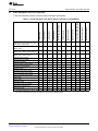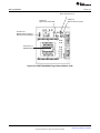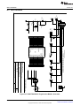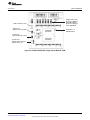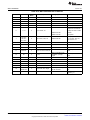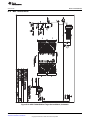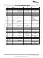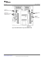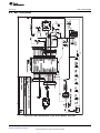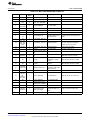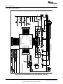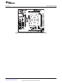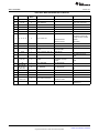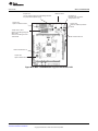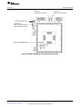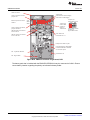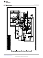
1
MSP430 Hardware Tools
User's Guide
Literature Number: SLAU278L
May 2009 – Revised December 2012
Contents
....................................................................................................................................... 7
Get Started Now! ............................................................................................................... 12
1.1
Flash Emulation Tool (FET) Overview .................................................................................. 13
1.2
Kit Contents, MSP-FET430PIF .......................................................................................... 14
1.3
Kit Contents, eZ430-F2013 .............................................................................................. 14
1.4
Kit Contents, eZ430-T2012 .............................................................................................. 14
1.5
Kit Contents, eZ430-RF2500 ............................................................................................ 14
1.6
Kit Contents, eZ430-RF2500T ........................................................................................... 14
1.7
Kit Contents, eZ430-RF2500-SEH ...................................................................................... 14
1.8
Kit Contents, eZ430-Chronos-xxx ....................................................................................... 15
1.9
Kit Contents, MSP-FET430UIF .......................................................................................... 15
1.10 Kit Contents, MSP-FET430xx ............................................................................................ 15
1.11 Kit Contents, FET430F6137RF900 ..................................................................................... 16
1.12 Kit Contents, Sub-1 GHz RF Spectrum Analyzer Tool (MSP-SA430-SUB1GHZ) ................................ 16
1.13 Kit Contents, MSP-TS430xx ............................................................................................. 17
1.14 Kit Contents, EM430Fx1x7RF900 ....................................................................................... 18
1.15 Hardware Installation, MSP-FET430PIF ............................................................................... 18
1.16 Hardware Installation, MSP-FET430UIF ............................................................................... 19
1.17 Hardware Installation, eZ430-XXXX, MSP-EXP430G2, MSP-EXP430FR5739, MSP-EXP430F5529 ......... 19
1.18 Hardware Installation, MSP-FET430Uxx, MSP-TS430xxx, FET430F6137RF900, EM430Fx137RF900 ...... 19
1.19 Important MSP430 Documents on the Web ........................................................................... 19
Design Considerations for In-Circuit Programming ............................................................... 20
2.1
Signal Connections for In-System Programming and Debugging ................................................... 21
2.2
External Power ............................................................................................................. 25
2.3
Bootstrap Loader (BSL) .................................................................................................. 25
Frequently Asked Questions and Known Issues ................................................................... 26
A.1
Hardware FAQs ............................................................................................................ 27
A.2
Known Issues .............................................................................................................. 29
Hardware .......................................................................................................................... 30
B.1
MSP-TS430D8 ............................................................................................................. 32
B.2
MSP-TS430PW14 ......................................................................................................... 35
B.3
MSP-TS430L092 .......................................................................................................... 38
B.4
MSP-TS430L092 Active Cable .......................................................................................... 41
B.5
MSP-TS430PW24 ......................................................................................................... 44
B.6
MSP-TS430DW28 ......................................................................................................... 47
B.7
MSP-TS430PW28 ......................................................................................................... 50
B.8
MSP-TS430PW28A ....................................................................................................... 53
B.9
MSP-TS430DA38 .......................................................................................................... 56
B.10 MSP-TS430QFN23x0 ..................................................................................................... 59
B.11 MSP-TS430RSB40 ........................................................................................................ 62
B.12 MSP-TS430RHA40A ...................................................................................................... 65
B.13 MSP-TS430DL48 .......................................................................................................... 68
B.14 MSP-TS430RGZ48B ...................................................................................................... 71
B.15 MSP-TS430RGZ48C ...................................................................................................... 74
Preface
1
2
A
B
2
Contents
SLAU278L – May 2009 – Revised December 2012
Submit Documentation Feedback
Copyright © 2009–2012, Texas Instruments Incorporated
www.ti.com
B.16
B.17
B.18
B.19
B.20
B.21
B.22
B.23
B.24
B.25
B.26
B.27
B.28
B.29
B.30
B.31
B.32
B.33
B.34
B.35
MSP-TS430PM64 ......................................................................................................... 77
MSP-TS430PM64A ....................................................................................................... 80
MSP-TS430RGC64B ..................................................................................................... 83
MSP-TS430RGC64C ..................................................................................................... 86
MSP-TS430RGC64USB .................................................................................................. 90
MSP-TS430PN80 .......................................................................................................... 94
MSP-TS430PN80A ........................................................................................................ 97
MSP-TS430PN80USB .................................................................................................. 100
MSP-TS430PZ100 ....................................................................................................... 104
MSP-TS430PZ100A ..................................................................................................... 107
MSP-TS430PZ100B ..................................................................................................... 110
MSP-TS430PZ100C ..................................................................................................... 113
MSP-TS430PZ5x100 .................................................................................................... 117
MSP-TS430PZ100USB ................................................................................................. 120
MSP-TS430PEU128 ..................................................................................................... 124
EM430F5137RF900 ..................................................................................................... 127
EM430F6137RF900 ..................................................................................................... 131
EM430F6147RF900 ..................................................................................................... 135
MSP-FET430PIF ......................................................................................................... 139
MSP-FET430UIF ......................................................................................................... 141
B.35.1 MSP-FET430UIF Revision History .......................................................................... 146
.............................................................................................. 147
.................................................................................................... 148
Document Revision History ........................................................................................................ 153
C
Hardware Installation Guide
C.1
Hardware Installation
SLAU278L – May 2009 – Revised December 2012
Submit Documentation Feedback
Copyright © 2009–2012, Texas Instruments Incorporated
Contents
3
www.ti.com
List of Figures
2-1.
Signal Connections for 4-Wire JTAG Communication ................................................................ 22
2-2.
Signal Connections for 2-Wire JTAG Communication (Spy-Bi-Wire) Used by MSP430F2xx,
MSP430G2xx and MSP430F4xx Devices .............................................................................. 23
2-3.
Signal Connections for 2-Wire JTAG Communication (Spy-Bi-Wire) Used by MSP430F5xx and
MSP430F6xx Devices .................................................................................................... 24
B-1.
MSP-TS430D8 Target Socket Module, Schematic
32
B-2.
MSP-TS430D8 Target Socket Module, PCB
33
B-3.
B-4.
B-5.
B-6.
B-7.
B-8.
B-9.
B-10.
B-11.
B-12.
B-13.
B-14.
B-15.
B-16.
B-17.
B-18.
B-19.
B-20.
B-21.
B-22.
B-23.
B-24.
B-25.
B-26.
B-27.
B-28.
B-29.
B-30.
B-31.
B-32.
B-33.
B-34.
B-35.
B-36.
B-37.
B-38.
B-39.
B-40.
B-41.
B-42.
B-43.
4
...................................................................
..........................................................................
MSP-TS430PW14 Target Socket Module, Schematic ...............................................................
MSP-TS430PW14 Target Socket Module, PCB ......................................................................
MSP-TS430L092 Target Socket Module, Schematic .................................................................
MSP-TS430L092 Target Socket Module, PCB ........................................................................
MSP-TS430L092 Active Cable Target Socket Module, Schematic .................................................
MSP-TS430L092 Active Cable Target Socket Module, PCB ........................................................
MSP-TS430PW24 Target Socket Module, Schematic ...............................................................
MSP-TS430PW24 Target Socket Module, PCB ......................................................................
MSP-TS430DW28 Target Socket Module, Schematic ...............................................................
MSP-TS430DW28 Target Socket Module, PCB ......................................................................
MSP-TS430PW28 Target Socket Module, Schematic ...............................................................
MSP-TS430PW28 Target Socket Module, PCB ......................................................................
MSP-TS430PW28A Target Socket Module, Schematic ..............................................................
MSP-TS430PW28A Target Socket Module, PCB (Red) .............................................................
MSP-TS430DA38 Target Socket Module, Schematic ................................................................
MSP-TS430DA38 Target Socket Module, PCB .......................................................................
MSP-TS430QFN23x0 Target Socket Module, Schematic ...........................................................
MSP-TS430QFN23x0 Target Socket Module, PCB ..................................................................
MSP-TS430RSB40 Target Socket Module, Schematic ..............................................................
MSP-TS430RSB40 Target Socket Module, PCB .....................................................................
MSP-TS430RHA40A Target Socket Module, Schematic ............................................................
MSP-TS430RHA40A Target Socket Module, PCB ...................................................................
MSP-TS430DL48 Target Socket Module, Schematic ................................................................
MSP-TS430DL48 Target Socket Module, PCB .......................................................................
MSP-TS430RGZ48B Target Socket Module, Schematic ............................................................
MSP-TS430RGZ48B Target Socket Module, PCB ...................................................................
MSP-TS430RGZ48C Target Socket Module, Schematic ............................................................
MSP-TS430RGZ48C Target Socket Module, PCB ...................................................................
MSP-TS430PM64 Target Socket Module, Schematic ................................................................
MSP-TS430PM64 Target Socket Module, PCB .......................................................................
MSP-TS430PM64A Target Socket Module, Schematic ..............................................................
MSP-TS430PM64A Target Socket Module, PCB .....................................................................
MSP-TS430RGC64B Target Socket Module, Schematic ............................................................
MSP-TS430RGC64B Target Socket Module, PCB ...................................................................
MSP-TS430RGC64C Target Socket Module, Schematic ............................................................
MSP-TS430RGC64C Target Socket Module, PCB ...................................................................
MSP-TS430RGC64USB Target Socket Module, Schematic ........................................................
MSP-TS430RGC64USB Target Socket Module, PCB ...............................................................
MSP-TS430PN80 Target Socket Module, Schematic ................................................................
MSP-TS430PN80 Target Socket Module, PCB .......................................................................
MSP-TS430PN80A Target Socket Module, Schematic ..............................................................
List of Figures
35
36
38
39
41
42
44
45
47
48
50
51
53
54
56
57
59
60
62
63
65
66
68
69
71
72
74
75
77
78
80
81
83
84
87
88
90
91
94
95
97
SLAU278L – May 2009 – Revised December 2012
Submit Documentation Feedback
Copyright © 2009–2012, Texas Instruments Incorporated
www.ti.com
B-44. MSP-TS430PN80A Target Socket Module, PCB ..................................................................... 98
B-45. MSP-TS430PN80USB Target Socket Module, Schematic ......................................................... 100
B-46. MSP-TS430PN80USB Target Socket Module, PCB ................................................................ 101
.............................................................
MSP-TS430PZ100 Target Socket Module, PCB ....................................................................
MSP-TS430PZ100A Target Socket Module, Schematic............................................................
MSP-TS430PZ100A Target Socket Module, PCB ...................................................................
MSP-TS430PZ100B Target Socket Module, Schematic............................................................
MSP-TS430PZ100B Target Socket Module, PCB ...................................................................
MSP-TS430PZ100C Target Socket Module, Schematic ...........................................................
MSP-TS430PZ100C Target Socket Module, PCB ..................................................................
MSP-TS430PZ5x100 Target Socket Module, Schematic ..........................................................
MSP-TS430PZ5x100 Target Socket Module, PCB..................................................................
MSP-TS430PZ100USB Target Socket Module, Schematic ........................................................
MSP-TS430PZ100USB Target Socket Module, PCB ...............................................................
MSP-TS430PEU128 Target Socket Module, Schematic ...........................................................
MSP-TS430PEU128 Target Socket Module, PCB ..................................................................
EM430F5137RF900 Target board, Schematic .......................................................................
EM430F5137RF900 Target board, PCB ..............................................................................
EM430F6137RF900 Target board, Schematic .......................................................................
EM430F6137RF900 Target board, PCB ..............................................................................
EM430F6147RF900 Target Board, Schematic ......................................................................
EM430F6147RF900 Target Board, PCB .............................................................................
MSP-FET430PIF FET Interface Module, Schematic ................................................................
MSP-FET430PIF FET Interface Module, PCB .......................................................................
MSP-FET430UIF USB Interface, Schematic (1 of 4) ...............................................................
MSP-FET430UIF USB Interface, Schematic (2 of 4) ...............................................................
MSP-FET430UIF USB Interface, Schematic (3 of 4) ...............................................................
MSP-FET430UIF USB Interface, Schematic (4 of 4) ...............................................................
MSP-FET430UIF USB Interface, PCB ................................................................................
Windows XP Hardware Wizard ........................................................................................
Windows XP Driver Location Selection Folder .......................................................................
Device Manager Using USB Debug Interface using VID/PID 0x2047/0x0010...................................
Device Manager Using USB Debug Interface with VID/PID 0x0451/0xF430 ....................................
Device Manager Using USB Debug Interface with VID/PID 0x0451/0xF432 ....................................
B-47. MSP-TS430PZ100 Target Socket Module, Schematic
104
B-48.
105
B-49.
B-50.
B-51.
B-52.
B-53.
B-54.
B-55.
B-56.
B-57.
B-58.
B-59.
B-60.
B-61.
B-62.
B-63.
B-64.
B-65.
B-66.
B-67.
B-68.
B-69.
B-70.
B-71.
B-72.
B-73.
C-1.
C-2.
C-3.
C-4.
C-5.
SLAU278L – May 2009 – Revised December 2012
Submit Documentation Feedback
Copyright © 2009–2012, Texas Instruments Incorporated
List of Figures
107
108
110
111
113
114
117
118
120
121
124
125
127
128
131
132
135
136
139
140
141
142
143
144
145
148
149
150
151
152
5
www.ti.com
List of Tables
1-1.
Flash Emulation Tool (FET) Features and Device Compatibility .................................................... 13
1-2.
Individual Kit Contents, MSP-TS430xx ................................................................................. 17
B-1.
MSP-TS430D8 Bill of Materials .......................................................................................... 34
B-2.
MSP-TS430PW14 Bill of Materials ...................................................................................... 37
B-3.
MSP-TS430L092 Bill of Materials ....................................................................................... 40
B-4.
MSP-TS430L092 JP1 Settings .......................................................................................... 42
B-5.
MSP-TS430L092 Active Cable Bill of Materials ....................................................................... 43
B-6.
MSP-TS430PW24 Bill of Materials ...................................................................................... 46
B-7.
MSP-TS430DW28 Bill of Materials...................................................................................... 49
B-8.
.....................................................................................
MSP-TS430PW28A Bill of Materials ....................................................................................
MSP-TS430DA38 Bill of Materials ......................................................................................
MSP-TS430QFN23x0 Bill of Materials..................................................................................
MSP-TS430RSB40 Bill of Materials ....................................................................................
MSP-TS430RHA40A Bill of Materials...................................................................................
MSP-TS430DL48 Bill of Materials .......................................................................................
MSP-TS430RGZ48B Bill of Materials...................................................................................
MSP-TS430RGZ48C Revision History .................................................................................
MSP-TS430RGZ48C Bill of Materials ..................................................................................
MSP-TS430PM64 Bill of Materials ......................................................................................
MSP-TS430PM64A Bill of Materials ....................................................................................
MSP-TS430RGC64B Bill of Materials ..................................................................................
MSP-TS430RGC64C Bill of Materials ..................................................................................
MSP-TS430RGC64USB Bill of Materials...............................................................................
MSP-TS430PN80 Bill of Materials ......................................................................................
MSP-TS430PN80A Bill of Materials ....................................................................................
MSP-TS430PN80USB Bill of Materials ...............................................................................
MSP-TS430PZ100 Bill of Materials ....................................................................................
MSP-TS430PZ100A Bill of Materials ..................................................................................
MSP-TS430PZ100B Bill of Materials ..................................................................................
MSP-TS430PZ100C Bill of Materials ..................................................................................
MSP-TS430PZ5x100 Bill of Materials .................................................................................
MSP-TS430PZ100USB Bill of Materials ..............................................................................
MSP-TS430PEU128 Bill of Materials .................................................................................
EM430F5137RF900 Bill of Materials ..................................................................................
EM430F6137RF900 Bill of Materials ..................................................................................
EM430F6147RF900 Bill of Materials ..................................................................................
USB VIDs and PIDs Used in MSP430 Tools .........................................................................
B-9.
B-10.
B-11.
B-12.
B-13.
B-14.
B-15.
B-16.
B-17.
B-18.
B-19.
B-20.
B-21.
B-22.
B-23.
B-24.
B-25.
B-26.
B-27.
B-28.
B-29.
B-30.
B-31.
B-32.
B-33.
B-34.
B-35.
C-1.
6
MSP-TS430PW28 Bill of Materials
List of Tables
52
55
58
61
64
67
70
73
75
76
79
82
85
89
92
96
99
102
106
109
112
115
119
122
126
129
133
137
148
SLAU278L – May 2009 – Revised December 2012
Submit Documentation Feedback
Copyright © 2009–2012, Texas Instruments Incorporated
Preface
SLAU278L – May 2009 – Revised December 2012
Read This First
About This Manual
This manual describes the hardware of the Texas Instruments MSP-FET430 Flash Emulation Tool (FET).
The FET is the program development tool for the MSP430 ultralow-power microcontroller. Both available
interface types, the parallel port interface and the USB interface, are described.
How to Use This Manual
Read and follow the instructions in Chapter 1. This chapter lists the contents of the FET, provides
instructions on installing the hardware and according software drivers. After you see how quick and easy it
is to use the development tools, TI recommends that you read all of this manual.
This manual describes the setup and operation of the FET but does not fully describe the MSP430™
microcontrollers or the development software systems. For details of these items, see the appropriate TI
documents listed in Section 1.19.
This manual applies to the following tools (and devices):
• MSP-FET430PIF (debug interface with parallel port connection, for all MSP430 flash-based devices)
• MSP-FET430UIF (debug interface with USB connection, for all MSP430 flash-based devices)
• eZ430-F2013 (USB stick form factor interface with attached MSP430F2013 target, for all
MSP430F20xx, MSP430G2x01, MSP430G2x11, MSP430G2x21, and MSP430G2x31 devices)
• eZ430-T2012 (three MSP430F2012 based target boards)
• eZ430-RF2500 (USB stick form factor interface with attached MSP430F2274 and CC2500 target, for
all MSP430F20xx, MSP430F21x2, MSP430F22xx, MSP430G2x01, MSP430G2x11, MSP430G2x21,
and MSP430G2x31 devices)
• eZ430-RF2500T (one MSP430F2274 and CC2500 target board including battery pack)
• eZ430-RF2500-SEH (USB stick form factor interface with attached MSP430F2274 and CC2500 target
and solar energy harvesting module)
• eZ430-Chronos-xxx (USB stick form factor interface with CC430F6137 based development system
contained in a watch. Includes <1 GHz RF USB access point)
The following tools contain the USB debug interface (MSP-FET430UIF) and the respective target socket
module:
• MSP-FET430U8 (for MSP430G2210 and MSP430G2230 devices in 8-pin D packages) (green PCB)
• MSP-FET430U14 (for MSP430F20xx, MSP430F20xx, MSP430G2x01, MSP430G2x11,
MSP430G2x21, and MSP430G2x31 devices in 14-pin PW packages) (green PCB)
•
•
•
•
•
•
•
•
•
•
MSP-FET430U092 (for MSP430FL092 devices in 14-pin PW packages) (green PCB)
MSP-FET430U24 (for MSP430AFE2xx devices in 24-pin PW packages) (green PCB)
MSP-FET430U28 (for MSP430F11xx(A) devices in 20- and 28-pin DW or PW packages)
MSP-FET430U28A (for MSP430F20xx and MSP430G2xxx devices in 14-, 20-, and 28-pin PW)
MSP-FET430U38 (for MSP430F22x2 and MSP430F22x4 devices in 38-pin DA packages)
MSP-FET430U23x0 (for MSP430F23x0 devices in 40-pin RHA packages)
MSP-FET430U40 (for MSP430F51x1, MSP430F51x2 devices in 40-pin RSB packages)
MSP-FET430U40A (for MSP430FR572x, MSP430FR573x devices in 40-pin RHA packages)
MSP-FET430U48 (for MSP430F22x2 and MSP430F22x4 devices in 48-pin DL packages)
MSP-FET430U48B (for MSP430F534x devices in 48-pin RGZ packages)
SLAU278L – May 2009 – Revised December 2012
Submit Documentation Feedback
Copyright © 2009–2012, Texas Instruments Incorporated
Read This First
7
How to Use This Manual
•
•
•
•
•
•
•
•
•
•
•
•
•
•
•
•
•
•
www.ti.com
MSP-FET430U48C (for MSP430FR58xx and MSP430FR59xx devices in 48-pin RGZ packages)
MSP-FET430U64 (for MSP430F13x, MSP430F14x, MSP430F14x1, MSP430F15x, MSP430F16x(1),
MSP430F23x, MSP430F24x, MSP430F24xx, MSP430F261x, MSP430F41x, MSP430F42x(A),
MSP430FE42x(A), MSP430FE42x2, and MSP430FW42x devices in 64-pin PM packages)
MSP-FET430U64A (for MSP430F41x2 devices in 64-pin PM packages) (red PCB)
MSP-FET430U64B (for MSP430F530x devices in 64-pin RGC packages) (blue PCB)
MSP-FET430U64C (for MSP430F522x and MSP430F521x devices in 64-pin RGC packages) (black
PCB)
MSP-FET430U64USB (for MSP430F550x, MSP430F551x, MSP430552x, devices in 64-pin RGC
packages)
MSP-FET430U80 (for MSP430F241x, MSP430F261x, MSP430F43x, MSP430F43x1, MSP430FG43x,
MSP430F47x, and MSP430FG47x devices in 80-pin PN packages)
MSP-FET430U80A (for MSP430F532x devices in 80-pin PN packages)
MSP-FET430U80USB (for MSP430F552x devices with USB peripheral in 80-pin PN packages)
MSP-FET430U100 (for MSP430F43x, MSP430F43x1, MSP430F44x, MSP430FG461x, and
MSP430F47xx devices in 100-pin PZ packages)
MSP-FET430U100A (for MSP430F471xx devices in 100-pin PZ packages) (red PCB)
MSP-FET430U100B (for MSP430F67xx devices in 100-pin PZ packages) (blue PCB)
MSP-FET430U100C (for MSP430F643x and MSP430F533x devices in 100-pin PZ packages) (black
PCB)
MSP-FET430U5x100 (for MSP430F54xx(A) devices and MSP430BT5190 in 100-pin PZ packages)
(green PCB)
MSP-FET430U100USB (for MSP430F663x and MSP430F563x devices in 100-pin PZ packages)
(green PCB)
MSP-FET430U128 (for MSP430F67xx and MSP430F67xx1 devices in 128-pin PEU packages) (green
PCB)
FET430F5137RF900 (for CC430F513x devices in 48-pin RGZ packages) (green PCB)
FET430F6137RF900 (for CC430F612x and CC430F613x devices in 64-pin RGC packages) (green
PCB)
Stand-alone target-socket modules (without debug interface):
• MSP-TS430D8 (for MSP430G2210 and MSP430G2230 devices in 8-pin D packages) (green PCB)
• MSP-TS430PW14 (for MSP430F20xx, MSP430G2x01, MSP430G2x11, MSP430G2x21 and
MSP430G2x31 devices in 14-pin PW packages) (green PCB)
• MSP-TS430L092 (for MSP430FL092 devices in 14-pin PW packages) (green PCB)
• MSP-TS430PW24 (for MSP430AFE2xx devices in 24-pin PW packages) (green PCB)
• MSP-TS430DW28 (for MSP430F11xx(A) devices in 28-pin DW packages) (green PCB)
• MSP-TS430PW28 (for MSP430F11xx(A) devices in 28-pin PW packages) (green PCB)
• MSP-TS430PW28A (for MSP430F20xx and MSP430G2xxx devices in 14, 20, and 28-pin PW) (red
PCB)
• MSP-TS430DA38 (for MSP430F22x2 and MSP430F22x4 devices in 38-pin DA packages) (green PCB)
• MSP-TS430QFN23x0 / MSP-TS430QFN40 (for MSP430F23x0 devices in 40-pin RHA packages)
(green PCB)
• MSP-TS430RSB40 (for MSP430F51x1, MSP430F51x2 devices in 40-pin RSB packages) (green PCB)
• MSP-TS430RHA40A (for MSP430FR572x, MSP430FR573x devices in 40-pin RHA packages) (red
PCB)
• MSP-TS430DL48 (for MSP430F22x2 and MSP430F22x4 devices in 48-pin DL packages) (green PCB)
• MSP-TS430RGZ48B (for MSP430F534x devices in 48-pin RGZ packages) (blue PCB)
• MSP-TS430RGZ48C (for MSP430FR58xx and MSP430FR59xx devices in 48-pin RGZ packages)
(black PCB)
8
Read This First
SLAU278L – May 2009 – Revised December 2012
Submit Documentation Feedback
Copyright © 2009–2012, Texas Instruments Incorporated
How to Use This Manual
www.ti.com
•
•
•
•
•
•
•
•
•
•
•
•
•
•
•
•
•
•
MSP-TS430PM64 (for MSP430F13x, MSP430F14x, MSP430F14x1, MSP430F15x, MSP430F16x(1),
MSP430F23x, MSP430F24x, MSP430F24xx, MSP430F261x, MSP430F41x, MSP430F42x(A),
MSP430FE42x(A), MSP430FE42x2, and MSP430FW42x devices in 64-pin PM packages) (green
PCB)
MSP-TS430PM64A (for MSP430F41x2 devices in 64-pin PM packages) (red PCB)
MSP-TS430RGC64B (for MSP430F530x devices in 64-pin RGC packages) (blue PCB)
MSP-TS430RGC64C (for MSP430F522x and MSP430F521x devices in 64-pin RGC packages) (black
PCB)
MSP-TS430RGC64USB (for MSP430F550x, MSP430F551x, MSP430F552x, devices in 64-pin RGC
packages) (green PCB)
MSP-TS430PN80 (for MSP430F241x, MSP430F261x, MSP430F43x, MSP430F43x1, MSP430FG43x,
MSP430F47x, and MSP430FG47x devices in 80-pin PN packages) (green PCB)
MSP-TS430PN80A (for MSP430F532x devices in 80-pin PN packages) (red PCB)
MSP-TS430PN80USB (for MSP430F551x and MSP430F552x devices with USB peripheral in 80-pin
PN packages) (green PCB)
MSP-TS430PZ100 (for MSP430F43x, MSP430F43x1, MSP430F44x, MSP430FG461x, and
MSP430F47xx devices in 100-pin PZ packages) (green PCB)
MSP-TS430PZ100A (for MSP430F471xx devices in 100-pin PZ packages) (red PCB)
MSP-FET430PZ100B (for MSP430F67xx devices in 100-pin PZ packages) (blue PCB)
MSP-TS430PZ100C (for MSP430F643x and MSP430F533x devices in 100-pin PZ packages) (black
PCB)
MSP-TS430PZ5x100 (for MSP430F54xx(A) and the MSP430BT5190 devices in 100-pin PZ packages)
(green PCB)
MSP-TS430PZ100USB (for MSP430F663x and MSP430F563x devices in 100-pin PZ packages)
(green PCB)
MSP-TS430PEU128 (for MSP430F67xx and MSP430F67xx1 devices in 128-pin PEU packages)
(green PCB)
EM430F5137RF900 (with integrated CC430F5137 IC in a 48-pin RGZ package) (green PCB)
EM430F6137RF900 (with integrated CC430F6137 IC in a 64-pin RGC package) (green PCB)
EM430F6147RF900 (with integrated CC430F6147 IC in a 64-pin RGC package) (red PCB)
These tools contain the most up-to-date materials available at the time of packaging. For the latest
materials (data sheets, user's guides, software, application information, etc.), visit the TI MSP430 web site
at www.ti.com/msp430 or contact your local TI sales office.
SLAU278L – May 2009 – Revised December 2012
Submit Documentation Feedback
Copyright © 2009–2012, Texas Instruments Incorporated
Read This First
9
Information About Cautions and Warnings
www.ti.com
Information About Cautions and Warnings
This document may contain cautions and warnings.
CAUTION
This is an example of a caution statement.
A caution statement describes a situation that could potentially damage your
software or equipment.
WARNING
This is an example of a warning statement.
A warning statement describes a situation that could potentially
cause harm to you.
The information in a caution or a warning is provided for your protection. Read each caution and warning
carefully.
Related Documentation From Texas Instruments
MSP430 development tools documentation:
CCS for MSP430 User's Guide (literature number SLAU157)
Code Composer Studio v5.x Core Edition (CCS Mediawiki)
IAR for MSP430 User's Guide (literature number SLAU138)
IAR Embedded Workbench KickStart (literature number SLAC050)
eZ430-F2013 Development Tool User's Guide (literature number SLAU176)
eZ430-RF2480 User's Guide (literature number SWRA176)
eZ430-RF2500 Development Tool User's Guide (literature number SLAU227)
eZ430-RF2500-SEH Development Tool User's Guide (literature number SLAU273)
eZ430-Chronos Development Tool User's Guide (literature number SLAU292)
Sub-1 GHz RF Spectrum Analyzer Tool (literature number SLAU371)
MSP430F5529 USB Experimenter’s Board, MSP-EXP430F5529 (literature number SLAU330)
MSP430F5438 Experimenter Board, MSP-EXP430F5438 (literature number SLAU263)
MSP430 LaunchPad Value Line Development kit, MSP-EXP430G2 (literature number SLAU318)
MSP430 device user's guides:
MSP430x1xx Family User's Guide (literature number SLAU049)
MSP430x2xx Family User's Guide (literature number SLAU144)
MSP430x3xx Family User's Guide (literature number SLAU012)
MSP430x4xx Family User's Guide (literature number SLAU056)
MSP430x5xx and MSP430x6xx Family User's Guide (literature number SLAU208)
CC430 Family User's Guide (literature number SLAU259)
MSP430FR57xx Family User's Guide (literature number SLAU272)
MSP430FR58xx and MSP430FR59xx Family User's Guide (literature number SLAU367)
10
Read This First
SLAU278L – May 2009 – Revised December 2012
Submit Documentation Feedback
Copyright © 2009–2012, Texas Instruments Incorporated
If You Need Assistance
www.ti.com
If You Need Assistance
Support for the MSP430 devices and the FET development tools is provided by the Texas Instruments
Product Information Center (PIC). Contact information for the PIC can be found on the TI web site at
www.ti.com/support. The Texas Instruments E2E Community support forums for the MSP430 provide
open interaction with peer engineers, TI engineers, and other experts. Additional device-specific
information can be found on the MSP430 web site.
SLAU278L – May 2009 – Revised December 2012
Submit Documentation Feedback
Copyright © 2009–2012, Texas Instruments Incorporated
Read This First
11
Chapter 1
SLAU278L – May 2009 – Revised December 2012
Get Started Now!
This chapter lists the contents of the FET and provides instruction on installing the hardware.
Topic
1.1
1.2
1.3
1.4
1.5
1.6
1.7
1.8
1.9
1.10
1.11
1.12
1.13
1.14
1.15
1.16
1.17
1.18
1.19
12
...........................................................................................................................
Flash Emulation Tool (FET) Overview ..................................................................
Kit Contents, MSP-FET430PIF .............................................................................
Kit Contents, eZ430-F2013 ..................................................................................
Kit Contents, eZ430-T2012 ..................................................................................
Kit Contents, eZ430-RF2500 ................................................................................
Kit Contents, eZ430-RF2500T ..............................................................................
Kit Contents, eZ430-RF2500-SEH ........................................................................
Kit Contents, eZ430-Chronos-xxx ........................................................................
Kit Contents, MSP-FET430UIF .............................................................................
Kit Contents, MSP-FET430xx ..............................................................................
Kit Contents, FET430F6137RF900 ........................................................................
Kit Contents, Sub-1 GHz RF Spectrum Analyzer Tool (MSP-SA430-SUB1GHZ) .........
Kit Contents, MSP-TS430xx ................................................................................
Kit Contents, EM430Fx1x7RF900 .........................................................................
Hardware Installation, MSP-FET430PIF ................................................................
Hardware Installation, MSP-FET430UIF ................................................................
Hardware Installation, eZ430-XXXX, MSP-EXP430G2, MSP-EXP430FR5739, MSPEXP430F5529 ....................................................................................................
Hardware Installation, MSP-FET430Uxx, MSP-TS430xxx, FET430F6137RF900,
EM430Fx137RF900 ............................................................................................
Important MSP430 Documents on the Web ...........................................................
Get Started Now!
Page
13
14
14
14
14
14
14
15
15
15
16
16
17
18
18
19
19
19
19
SLAU278L – May 2009 – Revised December 2012
Submit Documentation Feedback
Copyright © 2009–2012, Texas Instruments Incorporated
Flash Emulation Tool (FET) Overview
www.ti.com
1.1
Flash Emulation Tool (FET) Overview
TI offers several flash emulation tools according to different requirements.
Supports only F20xx, G2x01, G2x11,
G2x21, G2x31
x
Supports MSP430F20xx, F21x2, F22xx,
G2x01, G2x11, G2x21, G2x31, G2x53
x
Supports MSP430F20xx, F21x2, F22xx,
G2x01, G2x11, G2x21, G2x31
x
x
Supports F5438, F5438A
x
Supports BT5190, F5438A
x
Supports only F552x
x
Supports FR57xx, F5638, F6638
x
Supports only CC430F613x
x
Allows fuse blow
x
Adjustable target supply voltage
x
Fixed 2.8-V target supply voltage
x
Fixed 3.6-V target supply voltage
x
x
x
x
x
x
4-wire JTAG
x
2-wire JTAG (2)
x
Application UART
Supported by CCS for Windows
x
x
x
x
x
x
x
x
x
x
x
x
x
x
x
x
x
x
x
x
x
x
x
x
x
x
x
x
x
x
x
x
x
Supported by IAR
(2)
x
x
x
Supported by CCS for Linux
(1)
MSP-EXP430F5529
x
MSP-EXP430FR5739
x
LaunchPad (MSP-EXP430G2)
MSP-FET430UIF
Supports all MSP430 and CC430 flashbased devices (F1xx, F2xx, F4xx, F5xx,
F6xx, G2xx, L092, FR57xx)
MSP-FET430PIF
eZ430-Chronos
MSP-WDSxx Metawatch
eZ430-RF2560
eZ430-RF2480
eZ430-RF2500
eZ430-F2013
Table 1-1. Flash Emulation Tool (FET) Features and Device Compatibility (1)
x
x
x
x
x
x
x
x
The MSP-FET430PIF is for legacy device support only. This emulation tool will not support any new devices released after 2011.
The 2-wire JTAG debug interface is also referred to as Spy-Bi-Wire (SBW) interface.
SLAU278L – May 2009 – Revised December 2012
Submit Documentation Feedback
Copyright © 2009–2012, Texas Instruments Incorporated
Get Started Now!
13
Kit Contents, MSP-FET430PIF
1.2
www.ti.com
Kit Contents, MSP-FET430PIF
•
•
•
•
One
One
One
One
READ ME FIRST document
MSP-FET430PIF interface module
25-conductor cable
14-conductor cable
NOTE: This part is obsolete and is not recommended to use in new design.
1.3
Kit Contents, eZ430-F2013
•
•
1.4
Kit Contents, eZ430-T2012
•
1.5
QUICK START GUIDE document
eZ430-RF2500 CD-ROM
eZ430-RF2500 development tool including one MSP430F2274 and CC2500 target board
eZ430-RF2500T target board
AAA battery pack with expansion board (batteries included)
One eZ430-RF2500T target board
One AAA battery pack with expansion board (batteries included)
Kit Contents, eZ430-RF2500-SEH
•
•
•
•
•
14
One
One
One
One
One
Kit Contents, eZ430-RF2500T
•
•
1.7
Three MSP430F2012-based target boards
Kit Contents, eZ430-RF2500
•
•
•
•
•
1.6
One QUICK START GUIDE document
One eZ430-F2013 development tool including one MSP430F2013 target board
One MSP430 development tool CD containing documentation and development software
One eZ430-RF USB debugging interface
Two eZ430-RF2500T wireless target boards
One SEH-01 solar energy harvester board
One AAA battery pack with expansion board (batteries included)
Get Started Now!
SLAU278L – May 2009 – Revised December 2012
Submit Documentation Feedback
Copyright © 2009–2012, Texas Instruments Incorporated
Kit Contents, eZ430-Chronos-xxx
www.ti.com
1.8
Kit Contents, eZ430-Chronos-xxx
'433, '868, '915
• One QUICK START GUIDE document
• One ez430-Chronos emulator
• One screwdriver
• Two spare screws
eZ430-Chronos-433:
– One 433-MHz eZ430-Chronos watch (battery included)
– One 433-MHz eZ430-Chronos access point
eZ430-Chronos-868:
– One 868-MHz eZ430-Chronos watch (battery included)
– One 868-MHz eZ430-Chronos access point
eZ430-Chronos-915:
– One 915-MHz eZ430-Chronos watch (battery included)
– One 915-MHz eZ430-Chronos access point
1.9
Kit Contents, MSP-FET430UIF
•
•
•
•
One
One
One
One
READ ME FIRST document
MSP-FET430UIF interface module
USB cable
14-conductor cable
1.10 Kit Contents, MSP-FET430xx
'U8, 'U14, 'U092, 'U24, 'U28, 'U28A, 'U38, 'U23x0, 'U40, 'U40A, 'U48, 'U48B, 'U64, 'U64A, 'U64B,
'U64C, 'U64USB, 'U80, 'U80USB, 'U100, 'U100A, 'U100B, 'U100C, 'U5x100, 'U100USB, 'U128
• One READ ME FIRST document
• One MSP-FET430UIF USB interface module. This is the unit that has a USB B-connector on one end
of the case, and a 2×7-pin male connector on the other end of the case.
• One USB cable
• One 32.768-kHz crystal from Micro Crystal (except MSP-FET430U24)
• A 2×7-pin male JTAG connector is also present on the PCB (see different setup for L092)
• One 14-Pin JTAG conductor cable
• One small box containing two MSP430 device samples (See table for Sample Type)
• One target socket module. To check the devices used for each board and a summary of the board,
see Table 1-2. MSP-TS430xx below is the target socket module for each MSP-FET430Uxx kit.
MSP-FET430U8: One MSP-TS430D8 target socket module.
MSP-FET430U14: One MSP-TS430PW14 target socket module.
MSP-FET430U092: One MSP-TS430L092 target socket module with Active Cable.
MSP-FET430U24: One MSP-TS430PW24 target socket module.
MSP-FET430U28: One MSP-TS430PW28 target socket module.
MSP-FET430U28A: One MSP-TS430PW28A target socket module.
MSP-FET430U38: One MSP-TS430DA38 target socket module..
MSP-FET430U23x0: One MSP-TS430QFN23x0 (former name MSP-TS430QFN40) target socket
module.
MSP-FET430U40: One MSP-TS430RSB40 target socket module.
MSP-FET430U48: One MSP-TS430DL48 target socket module.
SLAU278L – May 2009 – Revised December 2012
Submit Documentation Feedback
Copyright © 2009–2012, Texas Instruments Incorporated
Get Started Now!
15
Kit Contents, FET430F6137RF900
www.ti.com
MSP-FET430U48B: One MSP-TS430RGZ48B target socket module.
MSP-FET430U48C: One MSP-TS430RGZ48C target socket module.
MSP-FET430U64: One MSP-TS430PM64 target socket module.
MSP-FET430U64A: One MSP-TS430PM64A target socket module.
MSP-FET430U64B: One MSP-TS430RGC64B target socket module.
MSP-FET430U64C: One MSP-TS430RGC64C target socket module.
MSP-FET430U64USB: One MSP-TS430RGC64USB target socket module.
MSP-FET430U80: One MSP-TS430PN80 target socket module.
MSP-FET430U80A: One MSP-TS430PN80A target socket module.
MSP-FET430U80USB: One MSP-TS430PN80USB target socket module.
MSP-FET430U100: One MSP-TS430PZ100 target socket module.
MSP-FET430U100A: One MSP-TS430PZ100A target socket module.
MSP-FET430U100B: One MSP-TS430PZ100B target socket module.
MSP-FET430U100C: One MSP-TS430PZ100C target socket module.
MSP-FET430U5x100: One MSP-TS430PZ5x100 target socket module.
MSP-FET430U100USB: One MSP-TS430PZ100USB target socket module.
MSP-FET430U128: One MSP-TS430PEU128 target socket module.
Consult the device data sheets for device specifications. Device errata can be found in the respective
device product folder on the web provided as a PDF document. Depending on the device, errata may also
be found in the device bug database at www.ti.com/sc/cgi-bin/buglist.cgi.
1.11 Kit Contents, FET430F6137RF900
•
•
•
•
•
•
•
•
•
•
•
One READ ME FIRST document
One legal notice
One MSP-FET430UIF interface module
Two EM430F6137RF900 target socket modules. This is the PCB on which is soldered a CC430F6137
device in a 64-pin RGC package. A 2×7-pin male connector is also present on the PCB
Two CC430EM battery packs
Four AAA batteries
Two 868-MHz or 915-MHz antennas
Two 32.768-kHz crystals
18 PCB 2x4-pin headers
One USB cable
One 14-pin JTAG conductor cable
1.12 Kit Contents, Sub-1 GHz RF Spectrum Analyzer Tool (MSP-SA430-SUB1GHZ)
•
•
•
•
•
16
MSP-SA430-SUB1GHZ Spectrum Analyzer
Antenna
USB cable
CD with a Microsoft Windows Graphical User Interface (GUI) and documentation
Quick start guide
Get Started Now!
SLAU278L – May 2009 – Revised December 2012
Submit Documentation Feedback
Copyright © 2009–2012, Texas Instruments Incorporated
Kit Contents, MSP-TS430xx
www.ti.com
1.13 Kit Contents, MSP-TS430xx
'D8, 'PW14, 'L092, 'PW24, 'DW28, 'PW28, 'PW28A, 'DA38, 'QFN32x0, 'RSB40, 'DL48, 'RGZ48B,
'RGZ48C, 'PM64, 'PM64A, 'RGC64B, 'RGC64C, 'RGC64USB, 'PN80, 'PN80A, 'PN80USB, 'PZ100,
'PZ100A, 'PZ100B, 'PZ100C, 'PZ5x100, 'PZ100USB, 'PEU128
• One READ ME FIRST document
• One 32.768-kHz crystal from Micro Crystal (except MSP-TS430PW24)
• One target socket module
• A 2×7-pin male JTAG connector is also present on the PCB (see different setup for L092)
• One small box containing two MSP430 device samples (see Table 1-2 for sample type)
Table 1-2. Individual Kit Contents, MSP-TS430xx
Target Socket Module
Socket Type
MSP-TS430D8
8-pin D
(TSSOP ZIF)
MSP-TS430PW14
14-pin PW
(TSSOP ZIF)
Supported Devices
Included Devices
Headers and Comment
MSP430G2210, G2230
1 x MSP430G2210 and
1 x MSP430G2230
Two PCB 1×4-pin headers (two male and
two female)
MSP430F20xx, G2x01,
G2x11, G2x21, G2x31
2 x MSP430F2013IPW
Four PCB 1×7-pin headers (two male and
two female)
MSP-TS430L092
14-pin PW
(TSSOP ZIF)
MSP-TS430L092
2 x MSP430L092IPW
Four PCB 1×7-pin headers (two male and
two female). A "Micro-MaTch" 10-pin
female connector is also present on the
PCB which connects the kit with an
'Active Cable' PCB; this 'Active Cable'
PCB is connected by 14 pin JTAG cable
with the FET430UIF
MSP-TS430PW24
24-pin PW
(TSSOP ZIF)
MSP430AFE2xx
2 x MSP430AFE253IPW
Four PCB 1×12-pin headers (two male
and two female)
MSP-TS430DW28
28-pin DW
(SSOP ZIF)
MSP-TS430PW28
28-pin PW
(TSSOP ZIF)
MSP430F11x1, F11x2,
F12x, F12x2, F21xx
MSP-TS430PW28A
28-pin PW
(TSSOP ZIF)
MSP430F20xx,
MSP430G2xxx in 14-, 20-,
and 28-pin PW packages
MSP-TS430DA38
38-pin DA
(TSSOP ZIF)
MSP-TS430QFN23x0
MSP430F11x1, F11x2,
F12x F12x2 F21xx.
2 x MSP430F123IDW
Supports devices in 20- and
28-pin DA packages
Four PCB 1×12-pin headers (two male
and two female)
2 x MSP430F2132IPW
Four PCB 1×12-pin headers (two male
and two female)
2 x MSP430G2452IPW20
Four PCB 1×12-pin headers (two male
and two female)
MSP430F22xx
2 x MSP430F2274IDA
Four PCB 1×19-pin headers (two male
and two female)
40-pin RHA
(QFN ZIF)
MSP430F23x0
2 x MSP430F2370IRHA
Eight PCB 1×10-pin headers (four male
and four female)
MSP-TS430RSB40
40-pin RSB
(QFN ZIF)
MSP430F51x1, F51x2
2 x MSP430F5172IRSB
Eight PCB 1×10-pin headers (four male
and four female)
MSP-TS430RHA40A
40-pin RHA
(QFN ZIF)
MSP430FR572x, FR573x
2 x MSP430FR5739IRHA
Eight PCB 1×10-pin headers (four male
and four female)
MSP-TS430DL48
48-pin DL
(TSSOP ZIF)
MSP430F42x0
2 x MSP430F4270IDL
Four PCB 2×12-pin headers (two male
and two female)
MSP-TS430RGZ48B
48-pin RGZ
(QFN ZIF)
MSP430F534x
2 x MSP430F5342IRGZ
Eight PCB 1×12-pin headers (four male
and four female)
MSP-TS430RGZ48C
48-pin RGZ
(QFN ZIF)
MSP430FR58xx and
MSP430FR59xx
2 x MSP430FR5969IRGZ
Eight PCB 1×12-pin headers (four male
and four female)
MSP-TS430PM64
64-pin PM
(QFP ZIF)
MSP430F13x, F14x, F14x1,
F15x, F16x(1), F23x, F24x,
F24xx, F261x, F41x,
F42x(A), FE42x(A), FE42x2,
FW42x
TS Kit:
2 x MSP430F2618IPM;
FET Kit:
2 x MSP430F417IPM and
2 x MSP430F169IPM
Eight PCB 1×16-pin headers (four male
and four female)
MSP-TS430PM64A
64-pin PM
(QFP ZIF)
MSP430F41x2
2 x MSP430F4152IPM
Eight PCB 1×16-pin headers (four male
and four female)
MSP-TS430RGC64B
64-pin RGC
(QFN ZIF)
MSP430F530x
2 x MSP430F5310IRGC
Eight PCB 1×16-pin headers (four male
and four female)
MSP-TS430RGC64C
64-pin RGC
(QFN ZIF)
MSP430F522x, F521x
2 x MSP430F5229IRGC
Eight PCB 1×16-pin headers (four male
and four female)
MSP-TS430RGC64USB
64-pin RGC
(QFN ZIF)
MSP430F550x, F551x,
F552x
2 x MSP430F5510IRGC or
2 x MSP430F5528IRGC
Eight PCB 1×16-pin headers (four male
and four female)
MSP-TS430PN80
80-pin PN
(QFP ZIF)
MSP430F241x, F261x,
F43x, F43x1, FG43x, F47x,
FG47x
2 x MSP430FG439IPN
Eight PCB 1×20-pin headers (four male
and four female)
SLAU278L – May 2009 – Revised December 2012
Submit Documentation Feedback
Copyright © 2009–2012, Texas Instruments Incorporated
Get Started Now!
17
Kit Contents, EM430Fx1x7RF900
www.ti.com
Table 1-2. Individual Kit Contents, MSP-TS430xx (continued)
Target Socket Module
Socket Type
MSP-TS430PN80A
80-pin PN
(QFP ZIF)
Supported Devices
Included Devices
MSP430F532x
2 x MSP430F5329IPN
Eight PCB 1×20-pin headers (four male
and four female)
MSP-TS430PN80USB
80-pin PN
(QFP ZIF)
MSP430F552x, F551x
2 x MSP430F5529IPN
Eight PCB 1×20-pin headers (four male
and four female)
MSP-TS430PZ100
100-pin PZ
(QFP ZIF)
MSP-TS430PZ100A
100-pin PZ
(QFP ZIF)
MSP430F471xx
2 x MSP430F47197IPZ
Eight PCB 1×25-pin headers (four male
and four female)
MSP-TS430PZ100B
100-pin PZ
(QFP ZIF)
MSP430F67xx
2 x MSP430F6733IPZ
Eight PCB 1×25-pin headers (four male
and four female)
MSP-TS430PZ100C
100-pin PZ
(QFP ZIF)
MSP430F645x, F643x,
F535x, F533x
2 x MSP430F6438IPZ
Eight PCB 1×25-pin headers (four male
and four female)
MSP-TS430PZ5x100
100-pin PZ
(QFP ZIF)
MSP430F543x,
MSP430BT5190,
MSP430SL5438A
2 x MSP430F5438IPZ
Eight PCB 1×25-pin headers (four male
and four female)
MSP-TS430PZ100USB
100-pin PZ
(QFP ZIF)
MSP430F665x, F663x,
F563x
2 x MSP430F6638IPZ
Eight PCB 1×25-pin headers (four male
and four female)
MSP-TS430PEU128
128-pin PEU
(QFP ZIF)
MSP430F677x, F676x,
F674x, F677x1, F676x1,
F674x1
2 x MSP430F67791IPEU
Four PCB 1x26-pin headers (two male
and two female) and four PCB 1x38-pin
headers (two male and two female)
MSP430F43x, F43x1, F44x,
2 x MSP430FG4619IPZ
FG461x, F47xx
Headers and Comment
Eight PCB 1×25-pin headers (four male
and four female)
See the device data sheets for device specifications. Device errata can be found in the respective device
product folder on the web provided as a PDF document. Depending on the device, errata may also be
found in the device bug database at www.ti.com/sc/cgi-bin/buglist.cgi.
1.14 Kit Contents, EM430Fx1x7RF900
•
•
•
•
•
•
•
•
One READ ME FIRST document
One legal notice
Two target socket module
MSP-EM430F5137RF900: Two EM430F5137RF900 target socket modules. This is the PCB on which
is soldered a CC430F5137 device in a 48-pin RGZ package. A 2×7-pin male connector is also present
on the PCB
MSP-EM430F6137RF900: Two EM430F6137RF900 target socket modules. This is the PCB on which
is soldered a CC430F6137 device in a 64-pin RGC package. A 2×7-pin male connector is also present
on the PCB
MSP-EM430F6147RF900: Two EM430F6147RF900 target socket modules. This is the PCB on which
is soldered a CC430F6147 device in a 64-pin RGC package. A 2×7-pin male connector is also present
on the PCB
Two CC430EM battery packs
Four AAA batteries
Two 868- or 915-MHz antennas
Two 32.768-kHz crystals
18 PCB 2×4-pin headers
1.15 Hardware Installation, MSP-FET430PIF
Follow these steps to install the hardware for the MSP-FET430PIF tools:
1. Use the 25-conductor cable to connect the FET interface module to the parallel port of the PC. The
necessary driver for accessing the PC parallel port is installed automatically during CCS or IAR
Embedded Workbench installation. Note that a restart is required after the CCS or IAR Embedded
Workbench installation for the driver to become active.
2. Use the 14-conductor cable to connect the parallel-port debug interface module to a target board, such
as an MSP-TS430xxx target socket module. Module schematics and PCBs are shown in Appendix B.
18
Get Started Now!
SLAU278L – May 2009 – Revised December 2012
Submit Documentation Feedback
Copyright © 2009–2012, Texas Instruments Incorporated
Hardware Installation, MSP-FET430UIF
www.ti.com
1.16 Hardware Installation, MSP-FET430UIF
Follow these steps to install the hardware for the MSP-FET430UIF tool:
1. Install the IDE (CCS or IAR) you plan to use before connecting USB-FET interface to PC. The IDE
installation installs drivers automatically.
2. Use the USB cable to connect the USB-FET interface module to a USB port on the PC. The USB FET
should be recognized, as the USB device driver is installed automatically. If the driver has not been
installed yet, the install wizard starts. Follow the prompts and point the wizard to the driver files.
The default location for CCS is c:\ti\ccsv5\ccs_base\emulation\drivers\msp430\USB_CDC or
c:\ti\ccsv5\ccs_base\emulation\drivers\msp430\USB_FET_XP_XX, depending of firmware version of
the tool.
The default location for IAR Embedded Workbench is <Installation Root>\Embedded Workbench x.x\
430\drivers\TIUSBFET\eZ430-UART or <Installation Root>\Embedded Workbench x.x\
430\drivers\<Win_OS>, depending of firmware version of the tool.
The USB driver is installed automatically. Detailed driver installation instructions can be found in
Appendix C.
3. After connecting to a PC, the USB FET performs a self-test during which the red LED may flash for
approximately two seconds. If the self-test passes successfully, the green LED stays on.
4. Use the 14-conductor cable to connect the USB-FET interface module to a target board, such as an
MSP-TS430xxx target socket module.
5. Ensure that the MSP430 device is securely seated in the socket, and that its pin 1 (indicated with a
circular indentation on the top surface) aligns with the "1" mark on the PCB.
6. Compared to the parallel-port debug interface, the USB FET has additional features including JTAG
security fuse blow and adjustable target VCC (1.8 V to 3.6 V). Supply the module with up to 60 mA.
1.17 Hardware Installation, eZ430-XXXX, MSP-EXP430G2, MSP-EXP430FR5739, MSPEXP430F5529
To install eZ430-XXXX, MSP-EXP430G2, MSP-EXP430FR5739, MSP-EXP430F5529 tools follow
instructions 1 and 2 of Section 1.16
1.18 Hardware Installation, MSP-FET430Uxx, MSP-TS430xxx, FET430F6137RF900,
EM430Fx137RF900
Follow these steps to install the hardware for the MSP-FET430Uxx and MSP-TS430xxx tools:
1. Follow instructions 1 and 2 of Section 1.16
2. Connect the MSP-FET430PIF or MSP-FET430UIF debug interface to the appropriate port of the PC.
Use the 14-conductor cable to connect the FET interface module to the supplied target socket module.
3. Ensure that the MSP430 device is securely seated in the socket and that its pin 1 (indicated with a
circular indentation on the top surface) aligns with the "1" mark on the PCB.
4. Ensure that the two jumpers (LED and VCC) near the 2×7-pin male connector are in place. Illustrations
of the target socket modules and their parts are found in Appendix B.
1.19 Important MSP430 Documents on the Web
The primary sources of MSP430 information are the device-specific data sheet and user's guide. The
MSP430 web site (www.ti.com/msp430) contains the most recent version of these documents.
PDF documents describing the CCS tools (CCS IDE, the assembler, the C compiler, the linker, and the
librarian) are in the msp430\documentation folder. A Code Composer Studio specific Wiki page (FAQ) is
available, and the Texas Instruments E2E Community support forums for the MSP430 and Code
Composer Studio v5 provide additional help besides the product help and Welcome page.
PDF documents describing the IAR tools (Workbench C-SPY, the assembler, the C compiler, the linker,
and the librarian) are in the common\doc and 430\doc folders. Supplements to the documents (that is, the
latest information) are available in HTML format in the same directories. A IAR specific Wiki Page is also
available.
SLAU278L – May 2009 – Revised December 2012
Submit Documentation Feedback
Copyright © 2009–2012, Texas Instruments Incorporated
Get Started Now!
19
Chapter 2
SLAU278L – May 2009 – Revised December 2012
Design Considerations for In-Circuit Programming
This chapter presents signal requirements for in-circuit programming of the MSP430.
Topic
2.1
2.2
2.3
20
...........................................................................................................................
Page
Signal Connections for In-System Programming and Debugging ............................ 21
External Power .................................................................................................. 25
Bootstrap Loader (BSL) ..................................................................................... 25
Design Considerations for In-Circuit Programming
SLAU278L – May 2009 – Revised December 2012
Submit Documentation Feedback
Copyright © 2009–2012, Texas Instruments Incorporated
Signal Connections for In-System Programming and Debugging
www.ti.com
2.1
Signal Connections for In-System Programming and Debugging
MSP-FET430PIF, MSP-FET430UIF, MSP-GANG, MSP-GANG430, MSP-PRGS430
With the proper connections, the debugger and an FET hardware JTAG interface (such as the MSPFET430PIF and MSP-FET430UIF) can be used to program and debug code on the target board. In
addition, the connections also support the MSP-GANG430 or MSP-PRGS430 production programmers,
thus providing an easy way to program prototype boards, if desired.
Figure 2-1 shows the connections between the 14-pin FET interface module connector and the target
device required to support in-system programming and debugging for 4-wire JTAG communication.
Figure 2-2 shows the connections for 2-wire JTAG mode (Spy-Bi-Wire). The 4-wire JTAG mode is
supported on most MSP430 devices except of small pin count devices e.g. MSP430G2230. The 2-wire
JTAG mode is available on selected devices only. See the CCS User's Guide for MSP430 (SLAU157) or
IAR for MSP430 User's Guide (SLAU138) for information on which interface method can be used on which
device.
The connections for the FET interface module and the MSP-GANG, MSP-GANG430 or MSP-PRGS430
are identical. Both the FET interface module and MSP-GANG430 can supply VCC to the target board (via
pin 2). In addition, the FET interface module, MSP-GANG and MSP-GANG430 have a VCC-sense feature
that, if used, requires an alternate connection (pin 4 instead of pin 2). The VCC-sense feature senses the
local VCC present on the target board (that is, a battery or other local power supply) and adjusts the output
signals accordingly. If the target board is to be powered by a local VCC, then the connection to pin 4 on the
JTAG should be made, and not the connection to pin 2. This utilizes the VCC-sense feature and prevents
any contention that might occur if the local on-board VCC were connected to the VCC supplied from the FET
interface module, MSP-GANG or the MSP-GANG430. If the VCC-sense feature is not necessary (that is, if
the target board is to be powered from the FET interface module, MSP-GANG or MSP-GANG430), the
VCC connection is made to pin 2 on the JTAG header and no connection is made to pin 4. Figure 2-1 and
Figure 2-2 show a jumper block that supports both scenarios of supplying VCC to the target board. If this
flexibility is not required, the desired VCC connections may be hard-wired eliminating the jumper block. Pins
2 and 4 must not be connected simultaneously.
Note that in 4-wire JTAG communication mode (see Figure 2-1), the connection of the target RST signal
to the JTAG connector is optional when using devices that support only 4-wire JTAG communication
mode. However, when using devices that support 2-wire JTAG communication mode in 4-wire JTAG
mode, the RST connection must be made. The MSP430 development tools and device programmers
perform a target reset by issuing a JTAG command to gain control over the device. However, if this is
unsuccessful, the RST signal of the JTAG connector may be used by the development tool or device
programmer as an additional way to assert a device reset.
SLAU278L – May 2009 – Revised December 2012
Submit Documentation Feedback
Design Considerations for In-Circuit Programming
Copyright © 2009–2012, Texas Instruments Incorporated
21
Signal Connections for In-System Programming and Debugging
www.ti.com
VCC
J1 (see Note A)
VCC/AVCC/DVCC
J2 (see Note A)
R1
47 kW
(see Note B)
C2
10 µF
C3
0.1 µF
MSP430Fxxx
JTAG
VCC TOOL
VCC TARGET
TEST/VPP
RST/NMI
2
1
4
3
6
5
8
7
10
9
12
11
14
13
TDO/TDI
TDO/TDI
TDI/VPP
TDI/VPP
TMS
TMS
TCK
TCK
GND
RST (see Note D)
TEST/VPP (see Note C)
C1
10 nF/2.2 nF
(see Notes B and E)
VSS/AVSS/DVSS
A
If a local target power supply is used, make connection J1. If power from the debug or programming adapter is used,
make connection J2.
B
The configuration of R1 and C1 for the RST/NMI pin depends on the device family. See the respective MSP430 family
user's guide for the recommended configuration.
C
The TEST pin is available only on MSP430 family members with multiplexed JTAG pins. See the device-specific data
sheet to determine if this pin is available.
D
The connection to the JTAG connector RST pin is optional when using 4-wire JTAG communication mode capableonly devices and not required for device programming or debugging. However, this connection is required when using
2-wire JTAG communication mode capable devices in 4-wire JTAG mode.
E
When using 2-wire JTAG communication capable devices in 4-wire JTAG mode, the upper limit for C1 should not
exceed 2.2 nF. This applies to both TI FET interface modules (LPT and USB FET).
Figure 2-1. Signal Connections for 4-Wire JTAG Communication
22
Design Considerations for In-Circuit Programming
SLAU278L – May 2009 – Revised December 2012
Submit Documentation Feedback
Copyright © 2009–2012, Texas Instruments Incorporated
Signal Connections for In-System Programming and Debugging
www.ti.com
VCC
J1 (see Note A)
VCC / AV CC / DVCC
J2 (see Note A)
R1
47kΩ
See Note B
C2
10μF
C3
0.1μF
MSP430Fxxx
JTAG
VCC TOOL
VCC TARGET
TEST/VPP
2
1
4
3
6
5
8
7
10
9
12
11
14
13
TDO/TDI
RST/NMI/SBWTDIO
TCK
GND
R2
330Ω
TEST/SBWTCK
C1
2.2 nF
See Note B
VSS / AV SS / DVSS
A
If a local target power supply is used, make connection J1. If power from the debug or programming adapter is used,
make connection J2.
B
The device RST/NMI/SBWTDIO pin is used in 2-wire mode for bidirectional communication with the device during
JTAG access, and any capacitance that is attached to this signal may affect the ability to establish a connection with
the device. The upper limit for C1 is 2.2 nF when using current TI tools.
C
R2 protects the JTAG debug interface TCK signal from the JTAG security fuse blow voltage that is supplied by the
TEST/VPP pin during the fuse blow process. If fuse blow functionality is not needed, R2 is not required (populate 0 Ω)
and do not connect TEST/VPP to TEST/SBWTCK.
Figure 2-2. Signal Connections for 2-Wire JTAG Communication (Spy-Bi-Wire) Used by MSP430F2xx,
MSP430G2xx and MSP430F4xx Devices
SLAU278L – May 2009 – Revised December 2012
Submit Documentation Feedback
Design Considerations for In-Circuit Programming
Copyright © 2009–2012, Texas Instruments Incorporated
23
Signal Connections for In-System Programming and Debugging
www.ti.com
VCC
J1 (see Note A)
VCC / AV CC / DVCC
J2 (see Note A)
R1
47kΩ
See Note B
C2
10µF
C3
0.1μF
MSP430Fxxx
JTAG
VCC TOOL
VCC TARGET
2
1
4
3
6
5
8
7
10
9
12
11
14
13
TDO/TDI
RST/NMI/SBWTDIO
TCK
GND
TEST/SBWTCK
C1
2.2 nF
See Note B
VSS / AV SS / DVSS
A
Make connection J1 if a local target power supply is used, or make connection J2 if the target is powered from the
debug or programming adapter.
B
The device RST/NMI/SBWTDIO pin is used in 2-wire mode for bidirectional communication with the device during
JTAG access, and any capacitance that is attached to this signal may affect the ability to establish a connection with
the device. The upper limit for C1 is 2.2 nF when using current TI tools.
Figure 2-3. Signal Connections for 2-Wire JTAG Communication (Spy-Bi-Wire) Used by MSP430F5xx and
MSP430F6xx Devices
24
Design Considerations for In-Circuit Programming
SLAU278L – May 2009 – Revised December 2012
Submit Documentation Feedback
Copyright © 2009–2012, Texas Instruments Incorporated
External Power
www.ti.com
2.2
External Power
The MSP-FET430UIF can supply targets with up to 60 mA through pin 2 of the 14-pin connector. Please
note that the target should not consume more than 60 mA, even as a peak current, as it may violate the
USB specification. E.g., if the target board has a capacitor on VCC more than 10 µF, it may cause inrush
current during capacitor charging that may exceed 60 mA. In this case the current should be limited by the
design of the target board, or an external power supply should be used.
The VCC for the target can be selected between 1.8 V and 3.6 V in steps of 0.1 V. Alternatively, the target
can be supplied externally. In this case, the external voltage should be connected to pin 4 of the 14-pin
connector. The MSP-FET430UIF then adjusts the level of the JTAG signals to external VCC automatically.
Only pin 2 (MSP-FET430UIF supplies target) or pin 4 (target is externally supplied) must be connected;
not both at the same time.
When a target socket module is powered from an external supply, the external supply powers the device
on the target socket module and any user circuitry connected to the target socket module, and the FET
interface module continues to be powered from the PC via the parallel port. If the externally supplied
voltage differs from that of the FET interface module, the target socket module must be modified so that
the externally supplied voltage is routed to the FET interface module (so that it may adjust its output
voltage levels accordingly). See the target socket module schematics in Appendix B.
The PC parallel port can source a limited amount of current. Because of the ultralow-power requirement of
the MSP430, a standalone FET does not exceed the available current. However, if additional circuitry is
added to the tool, this current limit could be exceeded. In this case, external power can be supplied to the
tool via connections provided on the target socket modules. See the schematics and pictorials of the
target socket modules in Appendix B to locate the external power connectors. Note that the MSPFET430PIF is not recommended for new design.
2.3
Bootstrap Loader (BSL)
The JTAG pins provide access to the flash memory of the MSP430Fxxx devices. On some devices, these
pins are shared with the device port pins, and this sharing of pins can complicate a design (or sharing may
not be possible). As an alternative to using the JTAG pins, most MSP430Fxxx devices contain a program
(a "bootstrap loader") that permits the flash memory to be erased and programmed using a reduced set of
signals. The MSP430 Programming Via the Bootstrap Loader User's Guide (SLAU319) describes this
interface. See the MSP430 web site for the application reports and a list of MSP430 BSL tool developers.
TI suggests that MSP430Fxxx customers design their circuits with the BSL in mind (that is, TI suggests
providing access to these signals by, for example, a header).
See FAQ Hardware #10 for a second alternative to sharing the JTAG and port pins.
SLAU278L – May 2009 – Revised December 2012
Submit Documentation Feedback
Design Considerations for In-Circuit Programming
Copyright © 2009–2012, Texas Instruments Incorporated
25
Appendix A
SLAU278L – May 2009 – Revised December 2012
Frequently Asked Questions and Known Issues
This appendix presents solutions to frequently asked questions regarding the MSP-FET430 hardware.
Topic
A.1
A.2
26
...........................................................................................................................
Page
Hardware FAQs ................................................................................................. 27
Known Issues ................................................................................................... 29
Frequently Asked Questions and Known Issues
SLAU278L – May 2009 – Revised December 2012
Submit Documentation Feedback
Copyright © 2009–2012, Texas Instruments Incorporated
Hardware FAQs
www.ti.com
A.1
Hardware FAQs
1. MSP430F22xx Target Socket Module (MSP-TS430DA38) – Important Information
Due to the large capacitive coupling introduced by the device socket between the adjacent signals
XIN/P2.6 (socket pin 6) and RST/SBWTDIO (socket pin 7), in-system debugging can disturb the
LFXT1 low-frequency crystal oscillator operation (ACLK). This behavior applies only to the Spy-Bi-Wire
(2-wire) JTAG configuration and only to the period while a debug session is active.
Workarounds:
• Use the 4-wire JTAG mode debug configuration instead of the Spy-Bi-Wire (2-wire) JTAG
configuration. This can be achieved by placing jumpers JP4 through JP9 accordingly.
• Use the debugger option "Run Free" that can be selected from the Advanced Run drop-down
menu (at top of Debug View). This prevents the debugger from accessing the MSP430 while the
application is running. Note that, in this mode, a manual halt is required to see if a breakpoint was
hit. See the IDE documentation for more information on this feature.
• Use an external clock source to drive XIN directly.
2. With current interface hardware and software, there is a weakness when adapting target boards
that are powered externally. This leads to an accidental fuse check in the MSP430. This is valid for
PIF and UIF but is mainly seen on UIF. A solution is being developed.
Workarounds:
• Connect RST/NMI pin to JTAG header (pin 11), LPT and USB tools are able to pull the RST line,
which also resets the device internal fuse logic.
• Use the debugger option "Release JTAG On Go" that can be selected from the IDE drop-down
menu. This prevents the debugger from accessing the MSP430 while the application is running.
Note that in this mode, a manual halt is required to see if a breakpoint was hit. See the IDE
documentation for more information on this feature.
• Use an external clock source to drive XIN directly.
3. The 14-conductor cable connecting the FET interface module and the target socket module must not
exceed 8 inches (20 centimeters) in length.
4. The signal assignment on the 14-conductor cable is identical for the parallel port interface and the
USB FET.
5. To utilize the on-chip ADC voltage references, the capacitor must be installed on the target
socket module. See schematic of the target socket module to populate the capacitor according to the
data sheet of the device.
6. To utilize the charge pump on the devices with LCD+ Module, the capacitor must be installed on
the target socket module. See schematic of the target socket module to populate the capacitor
according to the data sheet of the device.
7. Crystals or resonators Q1 and Q2 (if applicable) are not provided on the target socket module.
For MSP430 devices that contain user-selectable loading capacitors, see device and crystal data
sheets for the value of capacitance.
8. Crystals or resonators have no effect upon the operation of the tool and the CCS debugger or
C-SPY (as any required clocking and timing is derived from the internal DCO and FLL).
9. On devices with multiplexed port or JTAG pins, to use these pin in their port capability:
For CCS: "Run Free" (in Run pulldown menu at top of Debug View) must be selected.
For C-SPY: "Release JTAG On Go" must be selected.
10. As an alternative to sharing the JTAG and port pins (on low pin count devices), consider using
an MSP430 device that is a "superset" of the smaller device. A very powerful feature of the
MSP430 is that the family members are code and architecturally compatible, so code developed on
one device (for example, one without shared JTAG and port pins) ports effortlessly to another
(assuming an equivalent set of peripherals).
SLAU278L – May 2009 – Revised December 2012
Submit Documentation Feedback
Frequently Asked Questions and Known Issues
Copyright © 2009–2012, Texas Instruments Incorporated
27
Hardware FAQs
www.ti.com
11. Information memory may not be blank (erased to 0xFF) when the device is delivered from TI.
Customers should erase the information memory before its first use. Main memory of packaged
devices is blank when the device is delivered from TI.
12. The device current is higher then expected. The device current measurement may not be accurate
with the debugger connected to the device. For accurate measurement, disconnect the debugger.
13. The following ZIF sockets are used in the FET tools and target socket modules:
• 8-pin device (D package): Yamaichi IC369-0082
• 14-pin device (PW package): Enplas OTS-14-065-01
• 14-pin package for 'L092 (PW package): Yamaichi IC189-0142-146
• 24-pin package (PW package): Enplas OTS-24(28)-0.65-02
• 28-pin device (DW package): Wells-CTI 652 D028
• 28-pin device (PW package): Enplas OTS-28-0.65-01
• 38-pin device (DA package): Yamaichi IC189-0382-037
• 40-pin device (RHA package): Enplas QFN-40B-0.5-01
• 40-pin device (RSB package): Enplas QFN-40B-0.4
• 48-pin device (RGZ package): Yamaichi QFN11T048-008 A101121-001
• 48-pin device (DL package): Yamaichi IC51-0482-1163
• 64-pin device (PM package): Yamaichi IC51-0644-807
• 64-pin device (RGC package): Yamaichi QFN11T064-006
• 80-pin device (PN package): Yamaichi IC201-0804-014
• 100-pin device (PZ package): Yamaichi IC201-1004-008
• 128-pin device (PEU package): Yamaichi IC500-1284-009P
Enplas: www.enplas.com
Wells-CTI: www.wellscti.com
Yamaichi: www.yamaichi.us
28
Frequently Asked Questions and Known Issues
SLAU278L – May 2009 – Revised December 2012
Submit Documentation Feedback
Copyright © 2009–2012, Texas Instruments Incorporated
Known Issues
www.ti.com
A.2
Known Issues
MSP-FET430UIF
Current detection algorithm of the UIF firmware
Problem Description
If high current is detected, the ICC monitor algorithm stays in a loop of frequently
switching on and off the target power supply. This power switching puts some MSP430
devices such as the MSP430F5438 in a state that requires a power cycle to return the
device to JTAG control.
A side issue is that if the UIF firmware has entered this switch on and switch off loop, it
is not possible to turn off the power supply to the target by calling MSP430_VCC(0). A
power cycle is required to remove the device from this state.
Solution
IAR KickStart and Code Composer Essentials that have the MSP430.dll version
2.04.00.003 and higher do not show this problem. Update the software development tool
to this version or higher to update the MSP-FET430UIF firmware.
MSP-FET430PIF
Some PCs do not supply 5 V through the parallel port
Problem Description
Device identification problems with modern PCs, because the parallel port often does not
deliver 5 V as was common with earlier hardware.
1. When connected to a laptop, the test signal is clamped to 2.5 V.
2. When the external VCC becomes less than 3 V, up to 10 mA is flowing in the adapter
via pin 4 (sense).
Solution
Measure the voltage level of the parallel port. If it is too low, provide external 5 V to the
VCC pads of the interface. The jumper on a the target socket must be switched to
external power.
SLAU278L – May 2009 – Revised December 2012
Submit Documentation Feedback
Frequently Asked Questions and Known Issues
Copyright © 2009–2012, Texas Instruments Incorporated
29
Appendix B
SLAU278L – May 2009 – Revised December 2012
Hardware
This appendix contains information relating to the FET hardware, including schematics, PCB pictorials,
and bills of materials. All other tools, such as the eZ430 series, are described in separate product-specific
user's guides.
30
Hardware
SLAU278L – May 2009 – Revised December 2012
Submit Documentation Feedback
Copyright © 2009–2012, Texas Instruments Incorporated
Appendix B
www.ti.com
Topic
...........................................................................................................................
B.1
B.2
B.3
B.4
B.5
B.6
B.7
B.8
B.9
B.10
B.11
B.12
B.13
B.14
B.15
B.16
B.17
B.18
B.19
B.20
B.21
B.22
B.23
B.24
B.25
B.26
B.27
B.28
B.29
B.30
B.31
B.32
B.33
B.34
B.35
Page
MSP-TS430D8 ................................................................................................... 32
MSP-TS430PW14 ............................................................................................... 35
MSP-TS430L092 ................................................................................................ 38
MSP-TS430L092 Active Cable ............................................................................. 41
MSP-TS430PW24 ............................................................................................... 44
MSP-TS430DW28 ............................................................................................... 47
MSP-TS430PW28 ............................................................................................... 50
MSP-TS430PW28A ............................................................................................. 53
MSP-TS430DA38 ............................................................................................... 56
MSP-TS430QFN23x0 .......................................................................................... 59
MSP-TS430RSB40 ............................................................................................. 62
MSP-TS430RHA40A ........................................................................................... 65
MSP-TS430DL48 ................................................................................................ 68
MSP-TS430RGZ48B ........................................................................................... 71
MSP-TS430RGZ48C ........................................................................................... 74
MSP-TS430PM64 ............................................................................................... 77
MSP-TS430PM64A ............................................................................................. 80
MSP-TS430RGC64B ........................................................................................... 83
MSP-TS430RGC64C ........................................................................................... 86
MSP-TS430RGC64USB ....................................................................................... 90
MSP-TS430PN80 ............................................................................................... 94
MSP-TS430PN80A ............................................................................................. 97
MSP-TS430PN80USB ....................................................................................... 100
MSP-TS430PZ100 ............................................................................................ 104
MSP-TS430PZ100A .......................................................................................... 107
MSP-TS430PZ100B .......................................................................................... 110
MSP-TS430PZ100C .......................................................................................... 113
MSP-TS430PZ5x100 ......................................................................................... 117
MSP-TS430PZ100USB ...................................................................................... 120
MSP-TS430PEU128 .......................................................................................... 124
EM430F5137RF900 ........................................................................................... 127
EM430F6137RF900 ........................................................................................... 131
EM430F6147RF900 ........................................................................................... 135
MSP-FET430PIF ............................................................................................... 139
MSP-FET430UIF ............................................................................................... 141
SLAU278L – May 2009 – Revised December 2012
Submit Documentation Feedback
Copyright © 2009–2012, Texas Instruments Incorporated
Hardware
31
Vcc
J5
3
2
1
14
12
10
8
6
4
2
SBW
2
1
C7
13
11
9
7
5
3
1
GND
330R
R3
C5
100nF
SBWTCK
J4
R2
330R
1
2
3
4
TST/SBWTCK
FE4L
J1
VCC430
P1.2
P1.5
P1.6
U1
RST/SBWTDIO
R5
47K
MSP-TS430D8
DVCC
P1.2/TA1/A2
P1.5/TA0/A5/SCLK
P1.6/TA1/A6/SDO/SCL
DNP
GND
C8
2.2nF
1
2
3
4
Socket: YA MAICHI
Type: IC369-0082
DVSS
TST/SBWTCK
RST/SBWTDIO
P1.7/A7/SDI/SDA
8
7
6
5
GND
GND
TST/SBWTCK
RST/SBWTDIO
P1.7
J2
FE4H
8
7
6
5
VCC
J3
Ext_PWR
REV:
1.0
GND
1
2
3
Sheet: /11
Copyright © 2009–2012, Texas Instruments Incorporated
RST/SBWTDIO
TST/SBWTCK
to measure supply current
J6
10uF/10V
D1
green
2
1
ext
int
+
GND
MSP-TS430D8
MSP-TS430D8 Ta rget Socket Board
TITLE:
Document Number:
Date: 28.07.201
1 11:03:35
SLAU278L – May 2009 – Revised December 2012
Submit Documentation Feedback
Hardware
32
MSP-TS430D8
B.1
www.ti.com
MSP-TS430D8
Figure B-1. MSP-TS430D8 Target Socket Module, Schematic
MSP-TS430D8
www.ti.com
14 pin connector for debugging only
in Spy-Bi-Wire mode (4 Wire JTAG
not available)
D1 LED connected to P1.2
Connector J5
External power connector
Jumper JP3 to "ext"
Jumper JP2
Open to disconnect LED
Orient Pin 1 of MSP430 device
Figure B-2. MSP-TS430D8 Target Socket Module, PCB
SLAU278L – May 2009 – Revised December 2012
Submit Documentation Feedback
Copyright © 2009–2012, Texas Instruments Incorporated
Hardware
33
MSP-TS430D8
www.ti.com
Table B-1. MSP-TS430D8 Bill of Materials
Position
34
No. per
Board
Ref Des
Description
DigiKey Part No.
Comment
1
J4, J6
2
2-pin header, male, TH
SAM1035-02-ND
place jumper on header
2
J5
1
3-pin header, male, TH
SAM1035-03-ND
place jumper on pins 1-2
3
SBW
1
10-pin connector, male, TH
HRP10H-ND
4
J3
1
3-pin header, male, TH
SAM1035-03-ND
5
C8
1
2.2nF, CSMD0805
Buerklin 53 D 292
6
C7
1
10uF, 10V, 1210ELKO
478-3875-1-ND
7
R5
1
47K, 0805
541-47000ATR-ND
8
C5
1
100nF, CSMD0805
311-1245-2-ND
9
R2, R3
2
330R, 0805
541-330ATR-ND
10
J1, J2
2
4-pin header, TH
SAM1029-04-ND
DNP: headers enclosed with kit.
Keep vias free of solder.
10,1
J1, J2
1
4-pin socket, TH
SAM1029-04-ND
DNP: receptacles enclosed with
kit.
11
U1
1
SO8 Socket: Type IC369-0082
12
D1
1
red, LED 0603
13
MSP430
2
MSP430x
14
PCB
1
50,0mmx44,5mm
Hardware
Manuf.: Yamaichi
"DNP: enclosed with kit. Is
supplied by TI"
MSP-TS430D8 Rev.
1.0
SLAU278L – May 2009 – Revised December 2012
Submit Documentation Feedback
Copyright © 2009–2012, Texas Instruments Incorporated
MSP-TS430PW14
B.2
MSP-TS430PW14
www.ti.com
Vcc
J5
3
2
1
14
12
10
8
6
4
2
JTAG
13
11
9
7
5
3
1
GND
RST/NMI
SBWTCK
TMS
TDI
TDO/SBWTDIO
J7
3
2
1
TEST/SBWTCK
JTAG ->
SBW ->
XIN
XOUT
to measure supply current
J6
Q1
DNP
J4
R2
330R
1
2
3
4
5
6
7
TEST/SBWTCK
J1
J8
3
2
1
C8
2.2nF
1
2
3
4
5
6
7
J9
3
2
1
P1.7/TDO
3
2
1
J10
GND
XIN
XOUT
TEST/SBWTCK
RST/SBWTDIO
P1.7/TDO
P1.6/TDI
Socket: ENPLAS
Type: OTS-14-065
14
13
12
11
10
9
8
P1.6/TDI
14
13
12
11
10
9
8
J2
3
2
1
J11
VCC
P1.5/TMS
3
2
1
J12
2-wire "SpyBiWire": Set jumpers J7 to J12 to position 2-1
4-wire JTAG: Set jumpers J7 to J12 to position 2-3
JTAG-Mode selection:
RST/SBWTDIO
R5
47K
DNP
GND
VCC430
P1.0
P1.1
P1.2
P1.3
P1.4/TCK
P1.5/TMS
C3
100nF
DNP
GND
MSP-TS430PW14
Ext_PWR
J3
GND
P1.4/TCK
REV:
2.0
Sheet: 1/1
MSP-TS430PW14 Target Socket Board
TITLE:
Document Number:
Date: 7/16/2007 8:22:36 AM
Copyright © 2009–2012, Texas Instruments Incorporated
1
2
3
35
Hardware
SLAU278L – May 2009 – Revised December 2012
Submit Documentation Feedback
ext
int
2
1
12pF C2
DNP
330R
R3
12pF C1
DNP
D1
green
2
1
C5
C7
100nF
10uF/10V
GND
+
Figure B-3. MSP-TS430PW14 Target Socket Module, Schematic
MSP-TS430PW14
www.ti.com
Connector J3
External power connector
Jumper J5 to 'ext'
LED connected to P1.0
Jumpers J7 to J12
Close 1-2 to debug in
Spy-Bi-Wire Mode.
Close 2-3 to debug in
4-wire JTAG mode.
Jumper J4
Open to disconnect LED
Orient Pin 1 of
MSP430 device
Jumper J6
Open to measure current
Figure B-4. MSP-TS430PW14 Target Socket Module, PCB
36
Hardware
SLAU278L – May 2009 – Revised December 2012
Submit Documentation Feedback
Copyright © 2009–2012, Texas Instruments Incorporated
MSP-TS430PW14
www.ti.com
Table B-2. MSP-TS430PW14 Bill of Materials
Position
Ref Des
No. per
Board
1
C1, C2
0
12pF, SMD0805
511-1463-2-ND
478-3351-2-ND
Description
2
C7
1
10uF, 10V, Tantal Size
B
3
C3, C5
1
100nF, SMD0805
4
C8
0
2.2nF, SMD0805
5
D1
1
green LED, SMD0603
6
J1, J2
0
DigiKey Part No.
Comment
DNP
DNP: C3
DNP
475-1056-2-ND
DNP: Headers and receptacles
enclosed with kit. Keep vias free of
solder
7-pin header, TH
SAM1029-07-ND
: Header
SAM1213-07-ND
: Receptacle
7
J3, J5, J7,
J8, J9, J10,
J11, J12
8
3-pin header, male, TH
SAM1035-03-ND
Place jumpers on headers J5, J7, J8,
J9, J10, J11, J12; Pos 1-2
8
J4, J6
2
2-pin header, male, TH
SAM1035-02-ND
Place jumper on header
9
Jumper
15-38-1024-ND
Place on: J5, J7-J12; Pos 1-2
HRP14H-ND
9
10
JTAG
1
14-pin connector, male,
TH
12
Q1
0
Crystal
Micro Crystal MS1V-T1K
32.768kHz, C(Load) =
DNP: keep vias free of solder
12.5pF
13
R2, R3
2
330 Ω, SMD0805
541-330ATR-ND
15
R5
1
47k Ω, SMD0805
541-47000ATR-ND
16
U1
1
Socket: OTS-14-0.65-01
17
PCB
1
56 x 53 mm
18
Adhesive
plastic feet
4
Approximately 6mm
width, 2mm height
19
MSP430
2
MSP430F2013IPW
Manuf.: Enplas
2 layers
For example, 3M
Bumpons Part No. SJ5302
SLAU278L – May 2009 – Revised December 2012
Submit Documentation Feedback
Copyright © 2009–2012, Texas Instruments Incorporated
Apply to corners at bottom side
DNP: enclosed with kit, supplied by TI
Hardware
37
MSP-TS430L092
B.3
www.ti.com
MSP-TS430L092
Figure B-5. MSP-TS430L092 Target Socket Module, Schematic
38
Hardware
SLAU278L – May 2009 – Revised December 2012
Submit Documentation Feedback
Copyright © 2009–2012, Texas Instruments Incorporated
MSP-TS430L092
www.ti.com
Settings of the MSP-TS430L092 Target Socket
Figure B-6 shows the PCB layout of the MSP-TS430L092 target socket. The following pinning is
recommended:
• JP1 is write enable for the EPROM. If this is not set, the EPROM can only be read.
• JP2 and JP3 connect device supply with boost converter. They can be opened to measure device
current consumption. For default operation, they should be closed.
Figure B-6. MSP-TS430L092 Target Socket Module, PCB
SLAU278L – May 2009 – Revised December 2012
Submit Documentation Feedback
Copyright © 2009–2012, Texas Instruments Incorporated
Hardware
39
MSP-TS430L092
www.ti.com
Table B-3. MSP-TS430L092 Bill of Materials
Pos.
Ref Des No.
No. Per
Board
1
C1, C2
2
330nF, SMD0603
2
C5
1
100n, SMD0603
3
C6
1
10u, SMD0805
4
C10
1
100n, SMD0603
5
EEPROM1
1
M95512 SO08 (SO8)
7
40
J1, J2
2
Description
DigiKey Part No.
ST Micro M95160R
Comment
Digikey: 497-8688-1-ND
DNP: headers and
receptacles enclosed with kit.
Keep vias free of solder.
7-pin header, TH
SAM1213-07-ND
: Header
SAM1035-07-ND
: Receptacle
8
J3
1
3-pin header, male, TH
SAM1035-03-ND
9
J4, J5
2
FE4L, FE4H
4 pol. Stiftreihe
11
J13
1
MICRO_STECKV_10
12
JP1, JP2,JP3
3
2-pin header, male, TH
SAM1035-02-ND
place jumper on header
15
L1
1
33uH, SMD0806
LQH2MCN330K02L
Farnell: 151-5557
16
LED1, LED4
2
LEDCHIPLED_0603
17
Q2
1
BC817-16LT1SMD
18
R0, R6, R7
3
2K7, SMD0603
19
R1
1
1k, SMD0603
20
R2
1
47k, SMD0603
21
R4,R5, R8,
R10, RC, RD
6
10k, SMD0603
22
RA
1
3.9k, SMD0603
23
RB
1
6.8k, SMD0603
24
U1
1
14 Pin Socket - IC189-0142146
Manuf. Yamaichi
22
MSP430
2
MSP430L092PWR
DNP: Enclosed with kit. Is
supplied by TI.
Hardware
DNP; Keep vias free of
solder.
Reichelt: MicroMaTchConnector: MM FL 10G
Farnell: 1686065
BC817-16LT1SMD
SOT23-BEC
SLAU278L – May 2009 – Revised December 2012
Submit Documentation Feedback
Copyright © 2009–2012, Texas Instruments Incorporated
MSP-TS430L092 Active Cable
www.ti.com
B.4
MSP-TS430L092 Active Cable
Figure B-7. MSP-TS430L092 Active Cable Target Socket Module, Schematic
SLAU278L – May 2009 – Revised December 2012
Submit Documentation Feedback
Copyright © 2009–2012, Texas Instruments Incorporated
Hardware
41
MSP-TS430L092 Active Cable
www.ti.com
Figure B-8 shows the PCB layout for the Active Cable. The following pinning is possible:
• JP1 has two jumpers (Jumper 1 and Jumper 2) that can be set as shown in Table B-4.
Table B-4. MSP-TS430L092 JP1 Settings
•
Jumper 1
Jumper 2
Description
Off
Off
The active cable has no power and does not function.
Off
On
The active cable receives power from target socket. For this option, the
target socket must have its own power supply.
On
Off
The active cable receives power from the JTAG connector.
On
On
The JTAG connector powers the active cable and the target socket. For
this option, the target socket must not have its own power source, as this
would cause a not defined state.
JP2 is for reset. For the standard MSP-TS430L092, this jumper must be set. It sets the reset pin to
high and can also control it. Without this jumper on the MSP-TS430L092, reset is set to zero.
Figure B-8. MSP-TS430L092 Active Cable Target Socket Module, PCB
42
Hardware
SLAU278L – May 2009 – Revised December 2012
Submit Documentation Feedback
Copyright © 2009–2012, Texas Instruments Incorporated
MSP-TS430L092 Active Cable
www.ti.com
Table B-5. MSP-TS430L092 Active Cable Bill of Materials
Pos.
Ref Des
No. Per
Board
1
C1, C3, C5,
C6
4
100nF, SMD0603
2
C2, C4
2
1uF, SMD0805
3
R1, R10
2
10K, SMD0603
4
R2
1
4K7, SMD0603
5
R5, R6, R7,
R9
4
100, SMD0603
6
R8
1
680k, SMD0603
7
R11, R15
2
1K, SMD0603
8
R12
0
SMD0603
DNP
9
R13
0
SMD0603
DNP
10
R14
1
0, SMD0603
11
IC1
1
SN74AUC1G04DBVR
12
IC2, IC3, IC4
3
SN74AUC2G125DCTR
Description
DigiKey Part No.
Comment
Manu: TI
Manu: TI
13
J2
1
MICRO_STECKV_10
Reichelt: MicroMaTchConnector: MM FL 10G
14
JP1
1
2x2 Header
JP2Q
Put jumper on Position 1 and
2. Do not mix direction.
15
JP2
1
2-pin header, male, TH
SAM1035-02-ND
place jumper on header
16
JTAG
1
14-pin connector, male, TH
HRP14H-ND
17
Q1
1
BC817-25LT1SMD, SOT23BEC
Digi-Key: BC81725LT1GOSCT-ND
18
U1, U2
2
TLVH431IDBVR
SOT23-5
SLAU278L – May 2009 – Revised December 2012
Submit Documentation Feedback
Copyright © 2009–2012, Texas Instruments Incorporated
Manu: TI
Hardware
43
MSP-TS430PW24
B.5
www.ti.com
MSP-TS430PW24
Figure B-9. MSP-TS430PW24 Target Socket Module, Schematic
44
Hardware
SLAU278L – May 2009 – Revised December 2012
Submit Documentation Feedback
Copyright © 2009–2012, Texas Instruments Incorporated
MSP-TS430PW24
www.ti.com
Connector J5
External power connector
Jumper JP1 to "ext"
Jumper JP2
Open to measure current
Jumpers JP4 to JP9
Close 1-2 to debug in Spy-Bi-Wire mode
Close 2-3 to debug in 4-wire JTAG mode
Orient Pin 1 of MSP430 device
D1 LED connected to P1.0
Jumper JP3
Open to disconnect LED
Figure B-10. MSP-TS430PW24 Target Socket Module, PCB
SLAU278L – May 2009 – Revised December 2012
Submit Documentation Feedback
Copyright © 2009–2012, Texas Instruments Incorporated
Hardware
45
MSP-TS430PW24
www.ti.com
Table B-6. MSP-TS430PW24 Bill of Materials
Position
Ref Des
No. per
Board
1
C1, C2
0
12pF, SMD0805
2
C5
1
2.2nF, SMD0805
3
C3, C7
2
10uF, 10V, SMD0805
4
C4, C6, C8
3
100nF, SMD0805
478-3351-2-ND
5
D1
1
green LED, SMD0805
P516TR-ND
6
J1, J2
0
12-pin header, TH
"SAM1029-07NDSAM1213-07-ND"
DNP: Headers and receptacles
enclosed with kit. Keep vias free of
solder. (Header & Receptacle)
7
J5, JP1,
JP4, JP5,
JP6, JP7,
JP8, JP9
8
3-pin header, male, TH
SAM1035-03-ND
Place jumper on 1-2 of JP4-JP9
Place on 1-2 on JP1
8
JP2, JP3
2
2-pin header, male, TH
SAM1035-02-ND
Place jumper on header
9
Jumper
15-38-1024-ND
see Pos 7 an 8
HRP14H-ND
9
46
Description
DigiKey Part No.
Comment
DNP
10
JTAG
1
14-pin connector, male,
TH
11
Q1
0
Crystal
12
R1, R7
2
330 Ω, SMD0805
541-330ATR-ND
13
R5, R6,
R8, R9,
2
0 Ohm, SMD0805
541-000ATR-ND
14
R4
1
47k Ohm, SMD0805
541-47000ATR-ND
Manuf.: Enplas
2 layers
15
U1
1
Socket: OTS 24(28)065-02-00
16
PCB
1
68.5 x 61 mm
17
Adhesive
plastic feet
4
Approximately 6mm
width, 2mm height
18
MSP430
2
MSP430AFE2xx
Hardware
DNP: keep vias free of solder
for example, 3M
Bumpons Part No. SJ5302
DNP R5, R6
Apply to corners at bottom side
DNP: enclosed with kit, supplied by TI
SLAU278L – May 2009 – Revised December 2012
Submit Documentation Feedback
Copyright © 2009–2012, Texas Instruments Incorporated
MSP-TS430DW28
B.6
MSP-TS430DW28
www.ti.com
If external supply voltage:
-
R9
GND
C2
R8
0R
R2
0R
2
Q1
560R
R3
R1
-
12pF
C1
12pF
LED3
D1
14
12
10
8
6
4
2
JTAG
ML14
13
11
9
7
5
3
1
J5
JP1Q
28
27
26
25
24
23
22
21
20
19
18
17
16
15
1
C8
TDO
TDI
TMS
TCK
P1.3
P1.2
P1.1
P1.0
P2.4
P2.3
P3.7
P3.6
P3.5
P3.4
10nF
RST/NMI
C5
C7
100nF
10uF/10V
J4
JP1Q
SMD-Footprint
F123
TST/VPP 1
VCC430 2
3
P2.5
4
GND
5
XOUT
6
XIN
RST/NMI 7
8
P2.0
9
P2.1
10
P2.2
11
P3.0
12
P3.1
13
P3.2
14
P3.3
P1.7
P1.6
P1.5
P1.4
P1.3
P1.2
P1.1
P1.0
P2.4
P2.3
P3.7
P3.6
P3.5
P3.4
U2
TST
VCC
P2.5
VSS
XOUT
XIN
RST
P2.0
P2.1
P2.2
P3.0
P3.1
P3.2
P3.3
R5
50K
TST/VPP
VCC
TCK
TMS
TDI
TDO
U1
28
27
26
25
24
23
22
21
20
19
18
17
16
15
SOCK28DW
1
2
3
4
5
6
7
8
9
10
11
12
13
14
TDO
TDI
TMS
TCK
P1.3
P1.2
P1.1
P1.0
P2.4
P2.3
P3.7
P3.6
P3.5
P3.4
Socket: Yamaichi
Type: IC189-0282-042
TST/VPP
VCC430
P2.5
GND
XOUT
XIN
RST/NMI
P2.0
P2.1
P2.2
P3.0
P3.1
P3.2
P3.3
RST/NMI
1
2
3
4
5
6
7
8
9
10
11
12
13
14
FE14L
J1
J2
FE14H
28
27
26
25
24
23
22
21
20
19
18
17
16
15
R7
0R
R6
0R
TITLE:
J3
Ext_PWR
MSP-TS430DW28
Document Number:
R10 -
R11 0R
Sheet: 1/1
REV:
2.0
If external supply voltage:
remove R11 and add R10 (0 Ohm)
10
8
6
4 RST/NMI
2
ML10
not assembled
9
7
5
3
1
BOOTST
GND
1
2
3
MSP-TS430DW28 Target Socket DW28
GND
Date: 11/14/2006 1:26:04 PM
Copyright © 2009–2012, Texas Instruments Incorporated
47
Hardware
SLAU278L – May 2009 – Revised December 2012
Submit Documentation Feedback
remove R8 and add R9 (0 Ohm)
R1, C1, C2
not assembled
GND
2
1
+
QUARZ3
Figure B-11. MSP-TS430DW28 Target Socket Module, Schematic
MSP-TS430DW28
www.ti.com
LED connected to P1.0
Jumper J5
Open to measure current
Jumper J4
Open to disconnect LED
Connector J3
External power connector
Remove R8 and jumper R9
Orient Pin 1 of
MSP430 device
Figure B-12. MSP-TS430DW28 Target Socket Module, PCB
48
Hardware
SLAU278L – May 2009 – Revised December 2012
Submit Documentation Feedback
Copyright © 2009–2012, Texas Instruments Incorporated
MSP-TS430DW28
www.ti.com
Table B-7. MSP-TS430DW28 Bill of Materials
Position
Ref Des
No. per
Board
1
C1, C2
0
12pF, SMD0805
2
C5
1
100nF, SMD0805
3
C7
1
10uF, 10V Tantal Elko B
4
C8
1
10nF
SMD0805
5
D1
1
LED3 T1 3mm yellow
RS: 228-4991
6
Q1
0
QUARZ, Crystal
Micro Crystal MS1V-T1K
32.768kHz, C(Load) =
DNP: Cover holes while soldering
12.5pF
7
J1, J2
Description
2
DigiKey Part No.
Comment
DNP: C1, C2, Cover holes while
soldering
DNP: Headers and receptacles
enclosed with kit. Keep vias free of
solder.
14-pin header, TH male
: Header
: Receptacle
7.1
DNP: Headers and receptacles
enclosed with kit. Keep vias free of
solder.
14-pin header, TH
female
2
: Header
: Receptacle
8
J3
1
3-Pin Connector, male
9
J4, J5
2
2-Pin Connector, male
10
BOOTST
0
ML10, 10-Pin Conn., m
RS: 482-115
With jumper
11
JTAG
1
ML14, 14-Pin Conn., m
RS: 482-121
12
R1, R2,
R6, R7,
R8,R9,
R10, R11
4
0R, SMD0805
13
R3
1
560R, SMD0805
14
R5
1
47K, SMD0805
15
U1
1
SOP28DW socket
16
U2
0
TSSOP
DNP, Cover holes while soldering
DNP: R1, R2, R9, R10
Yamaichi: IC189-0282042
SLAU278L – May 2009 – Revised December 2012
Submit Documentation Feedback
Copyright © 2009–2012, Texas Instruments Incorporated
DNP
Hardware
49
Vcc
int
ext
3
2
1
C4
14
12
10
8
6
4
2
JTAG
13
11
9
7
5
3
1
VCC
P1.0
GND
JTAG ->
SBW ->
XOUT/P2.7
R6
0R
DNP
TEST/SBWTCK
100nF
R5
0R
XIN/P2.6
JP3
R4
47k
TST
VCC
P2.5
VSS
XOUT
XIN
RST
P2.0
P2.1
P2.2
P3.0
P3.1
P3.2
P3.3
U1
P1.7
P1.6
P1.5
P1.4
P1.3
P1.2
P1.1
P1.0
P2.4
P2.3
P3.7
P3.6
P3.5
P3.4
14
13
12
11
10
9
8
7
6
5
4
3
2
1
J2
JP6
GND
J5
-
DNP
R3 0R
R2
DNP
Ext_PWR
3
2 P1.4/TCK
1
JP9
10
8
6
4
2
DNP
GND
If external supply voltage:
remove R11 and add R10 (0 Ohm)
9
7
5
3
1
BOOTST
3
2 P1.5/TMS
1
JP8
RST/SBWTDIO
P1.1
TEST/SBWTCK
3
2 P1.6/TDI
1
JP7
3
2 P1.7/TDO
1
JTAG-Mode selection:
4-wire JTAG: Set jumpers JP4 to JP9 to position 2-3
2-wire "SpyBiWire": Set jumpers JP4 to JP9 to position 1-2
RST/SBWTDIO
C5
GND
P1.7/TDO
P1.6/TDI
P1.5/TMS
P1.4/TCK
P1.3
P1.2
P1.1
P1.0
P2.4
P2.3
P3.7
P3.6
P3.5
P3.4
DNP
2.2nF
28
27
26
25
24
23
22
21
20
19
18
17
16
15
P2.2
3
2
1
RST/NMI
TCK/SBWTCK
TMS
TDI
TDO/SBWTDIO
3
2
1
R7
330R
JP5
TEST/SBWTCK1
VCC430 2
3
P2.5
4
GND
XOUT/P2.75
XIN/P2.6 6
RST/SBWTDIO7
8
P2.0
9
P2.1
10
P2.2
11
P3.0
12
P3.1
13
P3.2
14
P3.3
TEST/SBWTCK
3
2
1
1
2
3
4
5
6
7
8
9
10
11
12
13
14
MSP430F12xx
JP4
J1
Socket: Enplas
OTS-28-0.65-01
MSP-TS430PW28:
Target Socket Board for MSP430's in PW28 package
3.1
Copyright © 2009–2012, Texas Instruments Incorporated
JP1
2
1
VCC430
C2
12pF
DNP
DNP
Q1
R1 330R
DNP
XTLGND
C1
12pF
D1
green
2
1
JP2
C3
10uF/10V
GND
+
GND
2
1
SLAU278L – May 2009 – Revised December 2012
Submit Documentation Feedback
Hardware
50
MSP-TS430PW28
B.7
www.ti.com
MSP-TS430PW28
Figure B-13. MSP-TS430PW28 Target Socket Module, Schematic
MSP-TS430PW28
www.ti.com
Jumper JP4 to JP9:
Close 1-2 to debug in Spy-Bi-Wire mode
Close 2-3 to debug in 4-wire JTAG mode
Jumper JP1
1-2 (int): Power supply via JTAG interface
2-3 (ext): External Power Supply
Jumper JP2
Open to measure current
Orient Pin 1 of Device
Jumper JP3
Open to disconnect LED
LED D1 connected to P5.1
Figure B-14. MSP-TS430PW28 Target Socket Module, PCB
SLAU278L – May 2009 – Revised December 2012
Submit Documentation Feedback
Copyright © 2009–2012, Texas Instruments Incorporated
Hardware
51
MSP-TS430PW28
www.ti.com
Table B-8. MSP-TS430PW28 Bill of Materials
Pos.
Ref Des
No. per
Board
1
C1, C2
0
12pF, SMD0805
2
C3
1
10uF, 10V Tantal Elko B
3
C4
1
100nF, SMD0805
4
C5
0
2.2nF, SMD0805
5
D1
1
LED green SMD0603
6
Q1
0
QUARZ, Crystal
7
J1, J2
2
Description
(1)
DigiKey Part No.
Comment
DNP: C1, C2 , Cover holes
while soldering
DNP
Micro Crystal MS1V-T1K
32.768kHz, C(Load) =
12.5pF
DNP: Cover holes and
neighboring holes while
soldering
DNP: Headers and
receptacles enclosed with
kit.Keep vias free of solder.
14-pin header, TH male
: Header
: Receptacle
7.1
2
DNP: headers and
receptacles enclosed with
kit.Keep vias free of solder.
14-pin header, TH female
: Header
: Receptacle
(1)
52
8
J5, IP1
1
3-Pin Connector , male
8a
JP1, JP4,
JP5, JP6,
JP7, JP8,
JP9
7
3-Pin Connector , male
Jumper on Pos 1-2
9
JP2, JP3
2
2-Pin Connector , male
with Jumper
10
BOOTST
0
ML10, 10-Pin Conn. , m
RS: 482-115
11
JTAG
1
ML14, 14-Pin Conn. , m
RS: 482-121
12
R1, R7
2
330R, SMD0805
12
R2, R3, R5,
R6
0
0R, SMD0805
14
R4
1
47K, SMD0805
15
U1
1
SOP28PW socket
DNP: Cover holes while
soldering
DNP
Enplas: OTS-28-0.65-01
PCB 66 x 79 mm, two layers; Rubber stand off, four pieces
Hardware
SLAU278L – May 2009 – Revised December 2012
Submit Documentation Feedback
Copyright © 2009–2012, Texas Instruments Incorporated
MSP-TS430PW28A
www.ti.com
B.8
MSP-TS430PW28A
Figure B-15. MSP-TS430PW28A Target Socket Module, Schematic
SLAU278L – May 2009 – Revised December 2012
Submit Documentation Feedback
Copyright © 2009–2012, Texas Instruments Incorporated
Hardware
53
MSP-TS430PW28A
www.ti.com
Jumper JP2
Open to measure current
Orient Pin 1 of MSP430 device
Connector J5
External power connector
Jumper JP1 to "ext"
Jumpers JP4 to JP9
Close 1-2 to debug in Spy-Bi-Wire mode
Close 2-3 to debug in 4-wire JTAG mode
Jumper JP3
Open to disconnect LED
D1 LED connected to P1.0
Figure B-16. MSP-TS430PW28A Target Socket Module, PCB (Red)
54
Hardware
SLAU278L – May 2009 – Revised December 2012
Submit Documentation Feedback
Copyright © 2009–2012, Texas Instruments Incorporated
MSP-TS430PW28A
www.ti.com
Table B-9. MSP-TS430PW28A Bill of Materials
Position
Ref Des
No. per
Board
1
C1, C2
0
12pF, SMD0805
2
C5
1
2.2nF, SMD0805
3
C3
1
10uF, 10V, SMD0805
4
C4, C6,
2
100nF, SMD0805
478-3351-2-ND
5
D1
1
green LED, SMD0805
P516TR-ND
6
J1, J2
0
14-pin header, TH
7
J5, JP1,
JP4, JP5,
JP6, JP7,
JP8, JP9
8
3-pin header, male, TH
SAM1035-03-ND
Place jumper on 1-2 of JP4-JP9
Place on 1-2 on JP1
8
JP2, JP3
2
2-pin header, male, TH
SAM1035-02-ND
Place jumper on header
9
Jumper
15-38-1024-ND
see Pos 7 an 8
14-pin connector, male,
TH
HRP14H-ND
9
Description
DigiKey Part No.
Comment
DNP
DNP: Headers and receptacles
enclosed with kit. Keep vias free of
solder: (Header & Receptacle)
10
JTAG
1
11
BOOTST
0
12
Q1
0
Crystal
Micro Crystal MS3V
32.768kHz, C(Load) =
12.5pF
13
R1, R7
2
330 Ω, SMD0805
541-330ATR-ND
14
R2, R3,R5,
R6,
0
0 Ohm, SMD0805
541-000ATR-ND
15
R4
1
47k Ω, SMD0805
541-47000ATR-ND
16
U1
1
Socket: OTS-28-0.65-01
17
PCB
1
63.5 x 64.8 mm
DNP Keep vias free of solder
18
Adhesive
plastic feet
4
Approximately 6mm
width, 2mm height
19
MSP430
2
MSP430G2553IPW28
DNP: keep vias free of solder
DNP R2, R3,R5, R6
Manuf.: Enplas
2 layers
for example, 3M
Bumpons Part No. SJ5302
SLAU278L – May 2009 – Revised December 2012
Submit Documentation Feedback
Copyright © 2009–2012, Texas Instruments Incorporated
Apply to corners at bottom side
DNP: enclosed with kit, supplied by TI
Hardware
55
Vcc
int
ext
3
2
1
14
12
10
8
6
4
2
JTAG
VCC430
C2
12pF
DNP
13
11
9
7
5
3
1
C5
100nF
GND
RST/NMI
TCK/SBWTCK
TMS
TDI
TDO/SBWTDIO
VCC
3
2
1
JP4
J1
TEST/SBWTCK
JTAG ->
SBW ->
P1.0
P2.7/XOUT
Q1 DNP
P2.6/XIN
R3 560R
R1
330R
38
37
36
35
34
33
32
31
30
29
28
27
26
25
24
23
22
21
20
P1.7/TDO 38
P1.6/TDI 37
P1.5/TMS 36
P1.4/TCK 35
34
P1.3
33
P1.2
32
P1.1
31
P1.0
30
P2.4
29
P2.3
28
P3.7
27
P3.6
26
P3.5
25
P3.4
24
P4.7
23
P4.6
22
P4.5
21
P4.4
20
P4.3
JP6
3
2 P1.7/TDO
1
3
2
1
JP8
3
2
1
J2
P2.2
3
2
1
JP9
DNP
GND
J3
DNP
R11 0R
R10 -
DNP
Ext_PWR
P1.4/TCK
10
8
6
4
2
BOOTST
9
7
5
3
1
REV:
1.3
GND
If external supply voltage:
remove R11 and add R10 (0 Ohm)
P1.5/TMS
RST/SBWTDIO
P1.1
TEST/SBWTCK
JP7
P1.6/TDI
JTAG-Mode selection:
4-wire JTAG: Set jumpers JP4 to JP9 to position 2-3
2-wire "SpyBiWire":Set jumpers JP4 to JP9 to position 2-1
DNP GND
R5
47k C8
10nF
U1
TEST/SBWTCK P1.7/TDO
DVCC
P1.6/TDI
P2.5
P1.5/TMS
DVSS
P1.4/TCK
P2.7
P1.3
P2.6
P1.2
RST/SBWDAT
P1.1
P2.0
P1.0
P2.1
P2.4
P2.2
P2.3
P3.0
P3.7
P3.1
P3.6
P3.2
P3.5
P3.3
P3.4
AVSS
P4.7
AVCC
P4.6
P4.0 Socket:
P4.5
P4.1 Yamaichi
P4.4
P4.2 IC189-0382-037P4.3
MSP430F2274IDA
RST/SBWTDIO
TEST/SBWTCK1
2
VCC430
3
P2.5
4
GND
5
P2.7/XOUT
6
P2.6/XIN
RST/SBWTDIO7
8
P2.0
9
P2.1
10
P2.2
11
P3.0
12
P3.1
13
P3.2
14
P3.3
15
GND
16
VCC430
17
P4.0
18
P4.1
19
P4.2
JP5
3
TEST/SBWTCK 2
1
1
2
3
4
5
6
7
8
9
10
11
12
13
14
15
16
17
18
19
3
2
1
Sheet: 1/1
Copyright © 2009–2012, Texas Instruments Incorporated
JP1
2
1
JP2
C7
10uF/10V
GND
C1
12pF
DNP
D1
yellow
JP3
2
1
+
GND
MSP-TS430DA38:
MSP-TS430DA38
Target Socket Board for MSP430F2247IDA
TITLE:
Document Number:
Date: 6/18/2008 11:04:56 AM
SLAU278L – May 2009 – Revised December 2012
Submit Documentation Feedback
Hardware
56
MSP-TS430DA38
B.9
www.ti.com
MSP-TS430DA38
Figure B-17. MSP-TS430DA38 Target Socket Module, Schematic
MSP-TS430DA38
www.ti.com
Jumpers JP4 to JP9
Close 1-2 to debug in
Spy-Bi-Wire Mode,
Close 2-3 to debug in
4-wire JTAG Mode
LED connected to P1.0
Jumper JP3
Open to disconnect LED
Orient pin 1 of
MSP430 device
Jumper JP2
Open to measure current
Connector J3
External power connector
Jumper JP1 to 'ext'
Figure B-18. MSP-TS430DA38 Target Socket Module, PCB
SLAU278L – May 2009 – Revised December 2012
Submit Documentation Feedback
Copyright © 2009–2012, Texas Instruments Incorporated
Hardware
57
MSP-TS430DA38
www.ti.com
Table B-10. MSP-TS430DA38 Bill of Materials
Pos.
Ref Des
No. per
Board
1
C1, C2
0
12pF, SMD0805
2
C7
1
10uF, 10V, Tantal Size B
511-1463-2-ND
3
C5
1
100nF, SMD0805
478-3351-2-ND
4
C8
0
2.2nF, SMD0805
5
D1
1
green LED, SMD0603
6
J1, J2
DigiKey Part No.
Comment
DNP
DNP
475-1056-2-ND
DNP: headers and
receptacles enclosed with
kit.Keep vias free of solder.
19-pin header, TH
SAM1029-19-ND
: Header
SAM1213-19-ND
: Receptacle
7
"J3, JP1,
JP4, JP5,
JP6, JP7,
JP8, JP9"
8
3-pin header, male, TH
SAM1035-03-ND
Place jumpers on headers
JP1, JP4,JP5, JP6, JP7,
JP8, JP9; Pos 1-2
8
JP2, JP3
2
2-pin header, male, TH
SAM1035-02-ND
Place jumper on header
9
Jumper
15-38-1024-ND
Place on: JP1 - JP9; Pos 12
HRP14H-ND
9
58
0
Description
10
JTAG
1
14-pin connector, male, TH
11
BOOTST
0
10-pin connector, male, TH
12
Q1
0
Crystal
Micro Crystal MS1V-T1K
32.768kHz, C(Load) =
12.5pF
13
R1, R3
2
330 Ω, SMD0805
541-330ATR-ND
14
R10, R11
0
0 Ω, SMD0805
541-000ATR-ND
15
R5
1
47k Ω, SMD0805
541-47000ATR-ND
16
U1
1
Socket: IC189-0382--037
17
PCB
1
67 x 66 mm
18
Adhesive
Plastic feet
4
~6mm width, 2mm height
19
MSP430
2
MSP430F2274IDA
Hardware
DNP: Keep vias free of
solder
DNP: Keep vias free of
solder
DNP
Manuf.: Yamaichi
2 layers
for example, 3M Bumpons
Part No. SJ-5302
Apply to corners at bottom
side
DNP: enclosed with kit
supplied by TI
SLAU278L – May 2009 – Revised December 2012
Submit Documentation Feedback
Copyright © 2009–2012, Texas Instruments Incorporated
MSP-TS430QFN23x0
www.ti.com
B.10 MSP-TS430QFN23x0
Figure B-19. MSP-TS430QFN23x0 Target Socket Module, Schematic
SLAU278L – May 2009 – Revised December 2012
Submit Documentation Feedback
Copyright © 2009–2012, Texas Instruments Incorporated
Hardware
59
MSP-TS430QFN23x0
www.ti.com
Connector J5
External power connector
Jumper JP1 to 'ext'
Jumper JP2
Open to measure current
Jumper JP3
Open to disconnect LED
LED connected
to P1.0
Figure B-20. MSP-TS430QFN23x0 Target Socket Module, PCB
60
Hardware
SLAU278L – May 2009 – Revised December 2012
Submit Documentation Feedback
Copyright © 2009–2012, Texas Instruments Incorporated
MSP-TS430QFN23x0
www.ti.com
Table B-11. MSP-TS430QFN23x0 Bill of Materials
Pos.
Ref Des
No. per
Board
1
C1, C2
0
12pF, SMD0805
2
C3
1
10uF, 10V, Tantal Size B
511-1463-2-ND
3
C4
1
100nF, SMD0805
478-3351-2-ND
4
C5
1
10nF, SMD0805
478-1383-2-ND
5
D1
1
green LED, SMD0603
475-1056-2-ND
6
J1, J2, J3,
J4
0
Description
DigiKey Part No.
Comment
DNP
DNP: headers and
receptacles enclosed with
kit.Keep vias free of solder.
10-pin header, TH
SAM1034-10-ND
: Header
SAM1212-10-ND
: Receptacle
7
J5, JP1
2
3-pin header, male, TH
SAM1035-03-ND
Place jumper on header
JP1; Pos 1-2.
8
JP2, JP3
2
2-pin header, male, TH
SAM1035-02-ND
Place jumper on header
Place on: JP1, JP2, JP3
3
Jumper
15-38-1024-ND
10
9
JTAG
1
14-pin connector, male, TH
HRP14H-ND
11
BOOTST
0
10-pin connector, male, TH
12
Q1
0
Crystal
Micro Crystal MS1V-T1K
32.768kHz, C(Load) =
12.5pF
13
R1
1
330 Ω, SMD0805
541-330ATR-ND
14
R2, R3
0
0 Ω, SMD0805
541-000ATR-ND
15
R4
1
47k Ω, SMD0805
541-47000ATR-ND
16
U1
1
Socket: QFN-40B-0.5-01
17
PCB
1
79 x 66 mm
18
Adhesive
Plastic feet
4
~6mm width, 2mm height
19
MSP430
2
MSP430F2370IRHA
DNP: Keep vias free of
solder
DNP: Keep vias free of
solder
DNP
Manuf.: Enplas
2 layers
for example, 3M Bumpons
Part No. SJ-5302
SLAU278L – May 2009 – Revised December 2012
Submit Documentation Feedback
Copyright © 2009–2012, Texas Instruments Incorporated
Apply to corners at bottom
side
DNP: enclosed with kit
supplied by TI
Hardware
61
MSP-TS430RSB40
www.ti.com
B.11 MSP-TS430RSB40
Figure B-21. MSP-TS430RSB40 Target Socket Module, Schematic
62
Hardware
SLAU278L – May 2009 – Revised December 2012
Submit Documentation Feedback
Copyright © 2009–2012, Texas Instruments Incorporated
MSP-TS430RSB40
www.ti.com
Connector J5
External power connector
Jumper JP1 to "ext"
Jumper JP2
Open to measure current
Jumpers JP4 to JP9
Close 1-2 to debug in Spy-Bi-Wire mode
Close 2-3 to debug in 4-wire JTAG mode
Orient Pin 1 of MSP430 device
Jumper JP3
Open to disconnect LED
D1 LED connected to P1.0
Figure B-22. MSP-TS430RSB40 Target Socket Module, PCB
SLAU278L – May 2009 – Revised December 2012
Submit Documentation Feedback
Copyright © 2009–2012, Texas Instruments Incorporated
Hardware
63
MSP-TS430RSB40
www.ti.com
Table B-12. MSP-TS430RSB40 Bill of Materials
Ref Des
No. Per
Board
Description
1
C1, C2
0
12pF, SMD0805
2
C3, C7, C10,
C12
3
10uF, 10V, SMD 0805
445-1371-1-ND
DNP C12
3
C4, C6, C8,
C11
3
100nF, SMD0805
311-1245-2-ND
DNP C11
4
C5
1
2.2nF, SMD0805
5
C9
1
470nF, SMD0805
6
D1
1
green LED, SMD0805
Pos.
7
J1, J2, J3, J4
4
DigiKey Part No.
Comment
DNP: C1, C2
P516TR-ND
DNP: headers and
receptacles enclosed with kit.
Keep vias free of solder.
10-pin header, TH
: Header
: Receptacle
7.1
4
DNP: headers and
receptacles enclosed with kit.
Keep vias free of solder.
10-pin header, TH
: Header
: Receptacle
8
JP1,
JP4,JP5,
JP6, JP7,
JP8, JP9, J5,
JP10
9
3-pin header, male, TH
SAM1035-03-ND
Jumper: 1-2 on JP1, JP10; 23 on JP4-JP9
9
JP2, JP3
2
2-pin header, male, TH
SAM1035-02-ND
place jumper on header
10
JTAG
1
14-pin connector, male, TH
HRP14H-ND
11
BOOTST
0
10-pin connector, male, TH
12
U1
1
QFN-40B-0.4_
ENPLAS_SOCKET
Enplas
13
Q1
0
Crystal
Micro Crystal MS3V-T1R
32.768kHz, C(Load) =
12.5pF
DNP: Q1. Keep vias free of
solder
10
Jumper
15-38-1024-ND
Place on: JP1, JP2, JP3,
JP4, JP5, JP6, JP7, JP8,
JP9, JP10
15
64
16
R1,R7
2
330R SMD0805
17
R2, R3, R5,
R6, R8, R9,
R10
3
0R SMD0805
18
R4
1
47k SMD0805
19
MSP430
2
MSP430F5132
20
Rubber stand
off
4
Hardware
DNP. Keep vias free of
solder
DNP R2, R3, R5, R6
DNP: enclosed with kit. Is
supplied by TI
select appropriate; for
example, Buerklin: 20H1724
apply to corners at bottom
side
SLAU278L – May 2009 – Revised December 2012
Submit Documentation Feedback
Copyright © 2009–2012, Texas Instruments Incorporated
MSP-TS430RHA40A
www.ti.com
B.12 MSP-TS430RHA40A
Figure B-23. MSP-TS430RHA40A Target Socket Module, Schematic
SLAU278L – May 2009 – Revised December 2012
Submit Documentation Feedback
Copyright © 2009–2012, Texas Instruments Incorporated
Hardware
65
MSP-TS430RHA40A
www.ti.com
Connector J5
External power connector
Jumper JP1 to "ext"
Jumper JP2
Open to measure current
Jumpers JP4 to JP9
Close 1-2 to debug in Spy-Bi-Wire mode
Close 2-3 to debug in 4-wire JTAG mode
D1 LED connected to P1.0
Jumper JP3
Open to disconnect LED
Orient Pin 1 of MSP430 device
Figure B-24. MSP-TS430RHA40A Target Socket Module, PCB
66
Hardware
SLAU278L – May 2009 – Revised December 2012
Submit Documentation Feedback
Copyright © 2009–2012, Texas Instruments Incorporated
MSP-TS430RHA40A
www.ti.com
Table B-13. MSP-TS430RHA40A Bill of Materials
Position
Ref Des
No. per
Board
1
C1, C2
0
12pF, SMD0805
DNP: C1, C2
2
C5
0
2.2nF, SMD0805
DNP C12
3
C3, C7
2
10uF, 10V, SMD0805 5
4
C4, C6
2
100nF, SMD0805
5
C9
1
470nF, SMD0805
6
D1
1
green LED, SMD0805
7
J1, J2, J3,
J4
Description
4
DigiKey Part No.
Comment
DNP C11
478-3351-2-ND
P516TR-ND
DNP: headers and receptacles
enclosed with kit. Keep vias free of
solder.
10-pin header, TH
: Header
: Receptacle
7.1
4
DNP: headers and receptacles
enclosed with kit. Keep vias free of
solder.
10-pin header, TH
: Header
: Receptacle
8
J5, JP1,
JP4, JP5,
JP6, JP7,
JP8, JP9
8
3-pin header, male, TH
SAM1035-03-ND
Place jumper on 1-2 of JP4-JP9;
Place on 1-2 on JP1
9
JP2, JP3
2
2-pin header, male, TH
SAM1035-02-ND
place jumper on header
9
Jumper
15-38-1024-ND
HRP14H-ND
10
see Pos 8 an 9
11
JTAG
1
14-pin connector, male,
TH
12
BOOTST
0
10-pin connector, male,
TH
DNP. Keep vias free of solder
13
U1
1
Socket: QFN-40B-0.5-01
Manuf.: Enplas
14
Q1
0
Crystal
15
R1,R7
2
330R SMD0805
541-330ATR-ND
16
R2, R3,
R5, R6,
R8, R9,
2
0 Ohm, SMD0805
541-000ATR-ND
17
R4
1
47k SMD0805
18
PCB
1
79 x 66 mm
19
Rubber
stand off
4
20
MSP430
2
Micro Crystal MS3V-T1R
32.768kHz, C(Load) = DNP: Q1. Keep vias free of solder
12.5pF
DNP:R2, R3, R5, R6
2 layers
select appropriate; for
example, Buerklin:
20H1724
MSP430N5736IRHA
SLAU278L – May 2009 – Revised December 2012
Submit Documentation Feedback
Copyright © 2009–2012, Texas Instruments Incorporated
apply to corners at bottom side
DNP: enclosed with kit. Is supplied by
TI
Hardware
67
ext
int
3
2
1
JP1
C7
10uF/10V
12pF
C2
560R
R3
12pF
C1
2
1
+
2
14
12
10
8
6
4
2
13
11
9
7
5
3
1
C8
10nF
TCK
TMS
TDI
TDO
GND
1
3
5
7
9
11
13
15
17
19
21
23
2
4
6
8
10
12
14
16
18
20
22
24
R5
47K
R4
0R
J1
RST/NMI
R12
0R
VCC
C3
100nF
C4
48
47
46
45
44
43
42
41
40
39
38
37
36
35
34
33
32
31
30
29
28 P1.0
27
26
25
IC51-1387.KS-15186
P5.4
P5.3
P5.2
COM0
P2.0
P2.1
P2.2
P2.3
P2.4
P2.5
P2.6
P2.7
S5
P5.7
P5.6
P5.5
P5.0
P5.1
LCDCAP
LCDREF
P1.0
P1.1
P1.2
P1.3
1
3
5
7
9
11
13
15
17
19
21
23
10uF/10V
J3
J2
GND
2
4
6
8
10
12
14
16
18
20
22
24
Ext_PWR
BSL_TX
0R
R7 0R
R6
MSP-TS430DL48
ML10
10
8
6
4
2
BOOTST
9
7
5
3
1
BSL_RX
Vcc
ext
int
JP2
RST/NMI
TCK
REV:
1.3
Sheet: 1/1
Copyright © 2009–2012, Texas Instruments Incorporated
JTAG
ML14
J5
JP1Q
P1.0
XOUT
C5
100nF
Q1
XIN
1
JP1Q
J4
TDO/TDI
TDI/TCLK
TMS
TCK
RST/NMI
DVCC
DVSS
XIN
XOUT
AVSS
AVCC
VREF+
P6.0
P6.1
P6.2
P6.3
P6.4
P6.5
P6.6
P6.7
P1.7
P1.6
P1.5
P1.4
GND
GND
1
2
3
MSP-TS430DL48 Target Socket DL48
TITLE:
Document Number:
1
2
3
GND
D1
LED3
QUARZ3
Vcc
Q1, C1, C2
not assembled
GND
TDO 1
2
TDI
TMS 3
TCK 4
RST/NMI 5
6
GND 7
8
XIN
XOUT 9
10
11
12
13
14
15
16
17
18
19
20
21
22
23
24
U1
+
Date: 11/14/2006 1:24:44 PM
SLAU278L – May 2009 – Revised December 2012
Submit Documentation Feedback
Hardware
68
www.ti.com
MSP-TS430DL48
B.13 MSP-TS430DL48
Figure B-25. MSP-TS430DL48 Target Socket Module, Schematic
MSP-TS430DL48
www.ti.com
Jumper J5
Open to measure current
LED connected
to P1.0
Connector J3
External power connector
Jumper JP1 to ‘ext’
Jumper J4
Open to
disconnect LED
Orient pin 1 of
MSP430 device
Figure B-26. MSP-TS430DL48 Target Socket Module, PCB
SLAU278L – May 2009 – Revised December 2012
Submit Documentation Feedback
Copyright © 2009–2012, Texas Instruments Incorporated
Hardware
69
MSP-TS430DL48
www.ti.com
Table B-14. MSP-TS430DL48 Bill of Materials
Pos.
Ref Des
No. per
Board
1
C1, C2
0
12pF, SMD0805
2
C4, C7
2
10uF, 10V, Tantal Size B
511-1463-2-ND
3
C3, C5
2
100nF, SMD0805
478-3351-2-ND
4
C8
1
10nF, SMD0805
478-1383-2-ND
5
D1
1
yellow LED, TH, 3mm, T1
511-1251-ND
6
J1, J2
DigiKey Part No.
Comment
DNP
DNP: Headers and
receptacles enclosed with
kit.Keep vias free of solder.
24-pin header, TH
SAM1034-12-ND
: Header
SAM1212-12-ND
: Receptacle
7
J3, JP1, JP2
2
3-pin header, male, TH
SAM1035-03-ND
Place jumper on header
JP1; Pos 1-2. DNP: JP2
8
J4, J5
2
2-pin header, male, TH
SAM1035-02-ND
Place jumper on header
Place on: JP1, J4, J5
9
70
0
Description
3
Jumper
15-38-1024-ND
10
JTAG
1
14-pin connector, male, TH
HRP14H-ND
11
BOOTST
0
10-pin connector, male, TH
12
Q1
0
Crystal
Micro Crystal MS1V-T1K
32.768kHz, C(Load) =
12.5pF
13
R3
1
560 Ω, SMD0805
541-560ATR-ND
14
R4, R6, R7,
R12
2
0 Ω, SMD0805
541-000ATR-ND
15
R5
1
47k Ω, SMD0805
541-47000ATR-ND
16
U1
1
Socket: IC51-1387 KS15186
Manuf.: Yamaichi
17
PCB
1
58 x 66 mm
2 layers
18
Adhesive
Plastic feet
4
~6mm width, 2mm height
19
MSP430
2
MSP430F4270IDL
Hardware
DNP: Keep vias free of
solder
for example, 3M Bumpons
Part No. SJ-5302
DNP: Keep vias free of
solder
DNP: R6, R7
Apply to corners at bottom
side
DNP: Enclosed with kit
supplied by TI
SLAU278L – May 2009 – Revised December 2012
Submit Documentation Feedback
Copyright © 2009–2012, Texas Instruments Incorporated
MSP-TS430RGZ48B
www.ti.com
B.14 MSP-TS430RGZ48B
Figure B-27. MSP-TS430RGZ48B Target Socket Module, Schematic
SLAU278L – May 2009 – Revised December 2012
Submit Documentation Feedback
Copyright © 2009–2012, Texas Instruments Incorporated
Hardware
71
MSP-TS430RGZ48B
www.ti.com
Connector J5
External power connector
Jumper JP1 to "ext"
Jumpers JP5 to JP10
Close 1-2 to debug in Spy-Bi-Wire mode
Close 2-3 to debug in 4-wire JTAG mode
Jumper JP1
Open to measure current
Orient Pin 1 of MSP430 device
Jumper JP2
Open to disconnect LED
D1 LED connected to P1.0
Figure B-28. MSP-TS430RGZ48B Target Socket Module, PCB
72
Hardware
SLAU278L – May 2009 – Revised December 2012
Submit Documentation Feedback
Copyright © 2009–2012, Texas Instruments Incorporated
MSP-TS430RGZ48B
www.ti.com
Table B-15. MSP-TS430RGZ48B Bill of Materials
Position
Ref Des
No. per
Board
1
C1, C2
0
12pF, SMD0805
DNP
2
C3, C4
0
47pF, SMD0805
DNP
3
C6, C7,
C12
3
10uF, 6.3V, SMD0805
4
C5, C11,
C13, C14
4
100nF, SMD0805
5
C8
1
2.2nF, SMD0805
6
C9
1
470nF, SMD0805
478-1403-2-ND
7
D1
1
green LED, SMD0805
P516TR-ND
8
J1, J2, J3,
J4
0
12-pin header, TH
SAM1029-12-ND
(Header) SAM1213-12ND (Receptacle)
DNP: Headers and receptacles
enclosed with kit. Keep vias free of
solder:
9
J5
1
3-pin header, male, TH
10
JP3, JP5,
JP6, JP7,
JP8, JP9,
JP10
7
3-pin header, male, TH
SAM1035-03-ND
place jumpers on pins 2-3 on JP5,
JP6, JP7, JP8, JP9, JP10 place
jumpers on pins 1-2 on JP3,
11
JP1, JP2
2
2-pin header, male, TH
SAM1035-02-ND
Place jumper on header
9
Jumper
15-38-1024-ND
See Pos. 10and Pos. 11
HRP14H-ND
12
Description
DigiKey Part No.
Comment
311-1245-2-ND
13
JTAG
1
14-pin connector, male,
TH
14
BOOTST
0
10-pin connector, male,
TH
15
Q1
0
Crystal
Micro Crystal MS3V-T1R
32.768kHz, C(Load) =
DNP: Q1 Keep vias free of solder
12.5pF
16
Q2
0
Crystal
Q2: 4MHz Buerklin:
78D134
17
Insulating
disk to Q2
0
Insulating disk to Q2
http://www.ettinger.de/Ar
t_Detail.cfm?ART_ART
NUM=70.08.121
18
R3, R7
2
330 Ω, SMD0805
541-330ATR-ND
19
R1, R2,
R4, R6,
R8,
R9,R10,
R11, R12
3
0 Ohm, SMD0805
541-000ATR-ND
20
R5
1
47k Ω, SMD0805
541-47000ATR-ND
21
U1
1
Socket: QFN11T048008_A101121_RGZ48
22
PCB
1
81 x 76 mm
23
Adhesive
plastic feet
4
Approximately 6mm
width, 2mm height
24
MSP430
2
MSP430F5342IRGZ
"DNP Keep vias free of solder"
DNP: Q2 Keep vias free of solder
DNP: R6, R8, R9, R10, R11,R12
Manuf.: Yamaichi
2 layers
for example, 3M
Bumpons Part No. SJ5302
SLAU278L – May 2009 – Revised December 2012
Submit Documentation Feedback
Copyright © 2009–2012, Texas Instruments Incorporated
Apply to corners at bottom side
DNP: enclosed with kit, supplied by TI
Hardware
73
Vcc
ext
int
J1
3
2
1
VCC
14
12
10
8
6
4
2
JTAG
13
11
9
7
5
3
1
GND
TEST/SBWTCK1
R7
0R
TEST/SBWTCK
JP4
3
2
1
DNP
GND
EVQ11
JP5
3
2 PJ.0/TDO
1
DNP
DVSS 12
P4.6 11
P4.5 10
P4.4 9
P1.7 8
P1.6 7
P3.7 6
P3.6 5
P3.5 4
P3.4 3
P2.2 2
P2.1 1
DNP
C9
JP7
GND
9
7
5
3
1
JP8
GND
J2
Ext_PWR
3
2 PJ.3/TCK
1
100nF
C6
DVCC
1uF/10V
DNP
C7
GND
10
8
6
4
2
DNP
If external supply voltage:
remove R3 and add R2 (0 Ohm)
DNP
BOOTST
3
2 PJ.2/TMS
1
HFGND
RST/SBWTDIO
P2.0
TEST/SBWTCK
P2.1
DNP
C8
DNP
JP6
SV2
3
2 PJ.1/TDI
1
JTAG-Mode selection:
4-wire JTAG: Set jumpers JP3 to JP8 to position 2-3
2-wire "SpyBiWire": Set jumpers JP3 to JP8 to position 1-2
SW1
1.1nF
C5
RST/SBWTDIO
47k
R4
HFXOUT
HFXIN
36
35
34
33
32
31
30
29
28
27
26
25
3
2
1
RST/NMI
JP3
3
2
1
TCK/SBWTCK
TMS
TDI
TDO/SBWTDIO
JTAG ->
U1
36_DVSS
35_P4.6
34_P4.5
33_P4.4
32_P1.7
31_P1.6
30_P3.7
29_P3.6
28_P3.5
27_P3.4
26_P2.2
25_P2.1
Target Socket Board for MSP430FR58xx, FR59xx IRGZ
MSP-TS430RGZ48C
1.3
Copyright © 2009–2012, Texas Instruments Incorporated
SBW ->
C2
DNP
LFXIN
LFXOUT
SV1
1_P1.0
2_P1.1
3_P1.2
4_P3.0
5_P3.1
6_P3.2
7_P3.3
8_P4.7
9_P1.3
10_P1.4
11_P1.5
12_PJ.0_TDO
QUARZ5
Q2
2
1
C4
DNP
1
P1.0
2
P1.1
3
P1.2
4
P3.0
5
P3.1
6
P3.2
7
P3.3
8
P4.7
9
P1.3
10
P1.4
11
P1.5
PJ.0/TDO 12
R8
0R
R9
0R
DVCC
AVCC
100nF
1
2
3
4
5
6
7
8
9
10
11
12
12
11
10
9
8
7
6
5
4
3
2
1
2
1
1uF/10V
C3
SV4
Q1
LFGND QUARZ5
DNP
C1
DNP
P1.3
P1.2
P1.1
P1.0
0R
R6
0R
R5
JP1
JP2
GND
DVCC
connection by via
AVSS
JP11
JP10
JP9
R2
-
R3
0R
0R R12
DVSS
DNP
SW2
0R R13
R14DNP
R11 DNP
D3
red (DNP)
R10DNP
R1 330R
D2
yellow (DNP)
D1
green
GND
SV3
TP1TP2
48 AVCC
47 AVSS
46
45
44 AVSS
43
42
41 AVSS
40 P2.4
39 P2.3
38 P2.7
37 DVCC
48_AVCC
47_AVSS
46_LFXOUT
45_LFXIN
44_AVSS
43_HFXOUT
42_HFXIN
41_AVSS
40_P2.4
39_P2.3
38_P2.7
37_DVCC
13_PJ.1_TDI
14_PJ.2_TMS
15_PJ.3/TCK
16_P4.0
17_P4.1
18_P4.2
19_P4.3
20_P2.5
21_P2.6
22_TEST/SBWTCK
23_RST/SBWTDIO
24_P2.0
1 PJ.1/TDI
13
2 PJ.2/TMS
14
3 PJ.3/TCK
15
4 P4.0
16
17
5 P4.1
18
6 P4.2
19
7 P4.3
20
8 P2.5
21
9 P2.6
10 TEST/SBWTCK22
11 RST/SBWTDIO23
24
12 P2.0
2
1
2
1
2
1
SLAU278L – May 2009 – Revised December 2012
Submit Documentation Feedback
Hardware
74
www.ti.com
MSP-TS430RGZ48C
B.15 MSP-TS430RGZ48C
Figure B-29. MSP-TS430RGZ48C Target Socket Module, Schematic
MSP-TS430RGZ48C
www.ti.com
Figure B-30. MSP-TS430RGZ48C Target Socket Module, PCB
Table B-16. MSP-TS430RGZ48C Revision History
Revision
Comments
1.2
Initial release
1.3
LFOSC pins swapped at SV1 (9-10).
HFOSC pins swapped at SV1 (6-7).
BOOTST pin 4 now directly connected to the device RST/SBWTDIO pin.
SLAU278L – May 2009 – Revised December 2012
Submit Documentation Feedback
Copyright © 2009–2012, Texas Instruments Incorporated
Hardware
75
MSP-TS430RGZ48C
www.ti.com
Table B-17. MSP-TS430RGZ48C Bill of Materials
Pos
1
Ref Des
SV1, SV2, SV3,
SV4
Number
Per
Board
4
Description
DigiKey Part Number
12-pin header, TH
Comment
DNP: headers and receptacles enclosed with kit.
Keep vias free of solder.
SAM1029-12-ND
: Header
: Receptacle
1.1
SV1, SV2, SV3,
SV4
4
12-pin receptable, TH
DNP: headers and receptacles enclosed with kit.
Keep vias free of solder.
: Header
76
SAM1213-12-ND
: Receptacle
2
JP1, JP2, JP9
3
2-pin header, male, TH
SAM1035-02-ND
Place jumper on header
3
JP10, JP11
2
2-pin header, male, TH
SAM1035-02-ND
DNP
4
J1, JP3, JP4, JP5,
JP6, JP7, JP8
7
3-pin header, male, TH
SAM1035-03-ND
Place jumpers on pins 2-3
5
J2
1
3-pin header, male, TH
SAM1035-03-ND
6
JP1, JP2, JP9, J1,
JP3, JP4, JP5,
JP6, JP7, JP8
10
Jumper
15-38-1024-ND
7
R2, R3, R5, R6,
R8, R9, R10, R11,
R14
9
DNP, 0805
8
R12, R13, R7
3
0R, 0805
541-000ATR-ND
9
C5
1
1.1nF, CSMD0805
490-1623-2-ND
10
C3, C7
2
1uF, 10V, CSMD0805
490-1702-2-ND
11
R4
1
47k, 0805
541-47000ATR-ND
12
C4, C6
2
100nF, CSMD0805
311-1245-2-ND
13
R1
1
330R, 0805
541-330ATR-ND
14
C1, C2, C8, C9
4
DNP, CSMD0805
15
SW1, SW2
2
EVQ-11L05R
P8079STB-ND
DNP, Lacon: 1251459
16
BOOTST
1
10-pin connector, male, TH
HRP10H-ND
DNP, keep vias free of solder
17
JTAG
1
14-pin connector, male, TH
HRP14H-ND
18
Q1
1
DNP: MS3V-TR1 (32768kHz,
20ppm, 12.5pF)
depends on application
Micro Crystal, DNP, enclosed in kit, keep vias
free of solder
19
Q2
1
DNP, Christal
depends on application
DNP, keep vias free of solder
20
U1
1
Socket: QFN11T048-008
A101121-001
Manuf.: Yamaichi
20.1
U1
1
MSP430
DNP: enclosed with kit. Is supplied by TI.
21
D1
1
green LED, DIODE0805
22
D3
1
red (DNP), DIODE0805
DNP
23
D2
1
yellow (DNP), DIODE0805
DNP
24
TP1, TP2
2
Testpoint
25
Rubber stand off
4
26
PCB
1
Hardware
79.6 x 91.0 mm
Place on: JP1, JP2, JP9, J1, JP3, JP4, JP5, JP6,
JP7, JP8
DNP
DNP
P516TR-ND
DNP, keep pads free of solder
Buerklin: 20H1724
apply to corners at bottom side
MSP-TS430RGZ48C
Rev. 1.2
2 layers, black solder mask
SLAU278L – May 2009 – Revised December 2012
Submit Documentation Feedback
Copyright © 2009–2012, Texas Instruments Incorporated
MSP-TS430PM64
www.ti.com
B.16 MSP-TS430PM64
12pF
C2
not assembled
R9
12pF
C1
R3
R4
2
14
12
10
8
6
4
2
1
13
11
9
7
5
3
1
J1
1
2
3
4
5
6
7
8
9
10
11
12
13
14
15
16
100nF
1
0R
R2
DVCC
2
3
4
5
6
7
XIN
XOUT
10
11
12
13
14
15
16
VCC
TCK
TMS
TDI
TDO
C8
R5
U2
MSP64PM
Socket:
Yamaichi
IC51-0644-807
RST/NMI
48
47
46
45
44
43
42
41
40
39
38
37
36
35
34
33
C3
12pF
not assembled
C4
12pF
48
47
46
45
44
43
42
41
40
39
38
37
36
35
34
33
J3
10
8
6
4
2
BOOTST
9
7
5
3
1
ML10
not assembled
J5
TITLE:
MSP-TS430PM64
Document Number:
PWR3
GND
1
2
3
For BSL usage add:
R11 0R
R6 R7 R13 R14
MSP430F14x : 0 0 open open
MSP430F41x : open open 0 0
If external supply voltage:
remove R11 and add R10 (0 Ohm)
R10 -
REV:
1.2
Sheet: 1/1
MSP-TS430PM64 Target Socket PM64
for F14x and F41x
FE16-1-3
GND
Date: 3/14/2006 10:46:30 AM
Copyright © 2009–2012, Texas Instruments Incorporated
10nF
47K
77
Hardware
SLAU278L – May 2009 – Revised December 2012
Submit Documentation Feedback
JTAG
ML14
J6
JP1Q
Open J6 if LCD
is connected
560R
2
remove R8 and add R9 (0 Ohm)
If external supply voltage:
GND
C5
FE16-1-1
0R
0R
0R
R14
0R
R7
R13
R6
FE16-1-4
XTCLK
J2
C7
+
R1 0R
64
63
62
61
60
59
58
57
56
55
54
53
52
51
50
49
AVCC
DVSS
AVSS
61
60
59
RST
TCK
TMS
TDI
TDO
53
52
51
50
49
17
18
19
20
21
22
23
24
25
26
27
28
29
30
31
32
17
18
19
20
21
22
23
24
25
26
27
28
29
30
31
32
10uF/10V
10uF/6,3V
+
C6
JP1Q
not assembled
J7
1
J4
FE16-1-2
-
LFXTCLK
0R
R12
Q1
-
R8
reserved for
future
enhancement
LED3
D1
NOTE: Connections between the JTAG header and pins XOUT and XIN are no longer required and should not be
made.
Figure B-31. MSP-TS430PM64 Target Socket Module, Schematic
MSP-TS430PM64
www.ti.com
Connector J5
External power connection
Remove R8 and jumper R9
LED connected
to pin 12
Jumper J7
Open to measure current
Jumper J6
Open to disconnect LED
Orient Pin 1 of
MSP430 device
Figure B-32. MSP-TS430PM64 Target Socket Module, PCB
78
Hardware
SLAU278L – May 2009 – Revised December 2012
Submit Documentation Feedback
Copyright © 2009–2012, Texas Instruments Incorporated
MSP-TS430PM64
www.ti.com
Table B-18. MSP-TS430PM64 Bill of Materials
Pos.
Ref Des
No. per
Board
1
C1, C2
0
12pF, SMD0805
DNP
1.1
C3, C4
0
47pF, SMD0805
DNP: Only recommendation.
Check your crystal spec.
2
C6, C7
1
10uF, 10V, Tantal Size B
511-1463-2-ND
3
C5
1
100nF, SMD0805
478-3351-2-ND
4
C8
1
10nF, SMD0805
478-1383-2-ND
5
C9
1
470nF, SMD0805
478-1403-2-ND
6
D1
1
green LED, SMD0805
P516TR-ND
7
J1, J2, J3, J4
0
Description
DigiKey Part No.
Comment
DNP: C6
DNP: Headers and
receptacles enclosed with
kit.Keep vias free of solder.
16-pin header, TH
SAM1029-16-ND
: Header
SAM1213-16-ND
: Receptacle
8
J5
1
3-pin header, male, TH
SAM1035-03-ND
9
J6, J7
2
2-pin header, male, TH
SAM1035-02-ND
Place jumper on header
2
Jumper
15-38-1024-ND
Place on: J6, J7
HRP14H-ND
11
12
JTAG
1
14-pin connector, male, TH
13
BOOTST
0
10-pin connector, male, TH
14
Q1, Q2
0
Crystal
Q1: Micro Crystal MS1V-T1K
DNP: Keep vias free of
32.768kHz, C(Load) =
solder
12.5pF
15
R3
1
330 Ω, SMD0805
541-330ATR-ND
16
R1, R2, R4,
R6, R7, R8,
R9, R10,
R11, R12,
R13, R14
3
0 Ω, SMD0805
541-000ATR-ND
17
R5
1
47k Ω, SMD0805
541-47000ATR-ND
18
U1
1
Socket: IC51-0644-807
Manuf.: Yamaichi
19
PCB
1
78 x 75 mm
2 layers
20
Rubber
standoff
4
21
MSP430
22
DNP: Keep vias free of
solder
select appropriate
MSP430F2619IPM
MSP430F417IPM
SLAU278L – May 2009 – Revised December 2012
Submit Documentation Feedback
Copyright © 2009–2012, Texas Instruments Incorporated
DNP: R4, R6, R7, R9, R10,
R11, R12, R13, R14
Apply to corners at bottom
side
DNP: Enclosed with kit
supplied by TI
Hardware
79
Vcc
3
2
ext
1
int
JP3
2
1
JP2
14
12
10
8
6
4
2
R2
0R
JTAG
C5
100nF
13
11
9
7
5
3
1
DNP
GND
J4
R6
330R
3
TEST/SBWTCK 2
A
1
JP5
RST/NMI
VCC
TCK/SBWTCK
TMS
TDI
TDO/SBWTDIO
3
2
1
JP4
AVCC
AVSS
Socket:
Yamaichi
IC51-0644-807
DNP GND
R4
47k C3
2.2nF
VCC430
RST/SBWTDIO
B
P1.0
P1.1
48
47
46
45
44
43
42
41
40
39
38
37
36
35
34
33
48
47
46
45
44
43
42
41
40
39
38
37
36
35
34
33
3
2 P7.0/TDO
1
C
JP6
J3
3
2
1
JP7
P7.1/TDI
D
DNP
R13
0R
TEST/SBWTCK
A
ADD LCD-CAP!
P5.1
3
2 P7.2/TMS
1 E
JP8
DNP
9
7
5
3
1
DNP
R11
0R
DNP
RST/SBWTDIO
B
DNP
R10
0R
PWR3
GND
1
2
3
3
2 P7.3/TCK
1 F
JP9
10
8
6
4
2
R14
0R BOOTST
GND
J5
Sheet: 1/1
REV:
1.1
If supplied by interface: populate R11 (0R), remove R10
If supplied locally: populate R10 (0R), remove R11
MSP-TS430PM64A
MSP-TS430PM64A Target Socket
for F4152
TITLE:
Document Number:
Date: 3/29/2011 3:07:02 PM
Copyright © 2009–2012, Texas Instruments Incorporated
JTAG ->
1
2
3
4
5
6
7
8
9
10
11
12
13
14
15
16
SBW ->
AVCC
J1
VCC430
AVSS
C4
100nF
0R
R7
XIN
Q1
1
2
3
4
5
6
7
8
9
10
11
12
13
14
15
16
GND
J2
A
B
F
E
D
C
VCC430
C6
10uF/6.3V
R1 0R
DNP
12pF
C2
DNP
R5
0R
XOUT
DNP
R3
P5.1
330R
JP1
Open JP1 if LCD
is connected
DNP
12pF
C1
XTLGND
GND
D1
2
1
+
GND
1
2
64
63
62
61
60
59
58
57
56
55
54
53
52
51
50
49
64
63
62
61
60
59
58
57
56
55
54
53
52
51
50
49
17
18
19
20
21
22
23
24
25
26
27
28
29
30
31
32
17
18
19
20
21
22
23
24
25
26
27
28
29
30
31
32
SLAU278L – May 2009 – Revised December 2012
Submit Documentation Feedback
Hardware
80
www.ti.com
MSP-TS430PM64A
B.17 MSP-TS430PM64A
Figure B-33. MSP-TS430PM64A Target Socket Module, Schematic
MSP-TS430PM64A
www.ti.com
Jumper JP3
1-2 (int): Power supply via JTAG interface
2-3 (ext): External Power Supply
Jumper JP4 to JP9:
Close 1-2 to debug in Spy-Bi-Wire mode
Close 2-3 to debug in 4-wire JTAG mode
Jumper JP2
Open to measure current
Orient Pin 1 of Device
Jumper JP1
Open to disconnect LED
LED D1 connected to P5.1
Figure B-34. MSP-TS430PM64A Target Socket Module, PCB
SLAU278L – May 2009 – Revised December 2012
Submit Documentation Feedback
Copyright © 2009–2012, Texas Instruments Incorporated
Hardware
81
MSP-TS430PM64A
www.ti.com
Table B-19. MSP-TS430PM64A Bill of Materials
Pos.
Ref Des
No. per
Board
1
C1, C2,
0
12pF, SMD0805
DNP
2
C3
0
2.2nF, SMD0805
DNP
3
C6,
1
10uF, 10V, Tantal Size B
511-1463-2-ND
4
C4, C5
2
100nF, SMD0805
478-3351-2-ND
5
D1
1
green LED, SMD0805
P516TR-ND
6
J1, J2, J3, J4
DigiKey Part No.
Comment
DNP: Headers and
receptacles enclosed with kit.
Keep vias free of solder.
16-pin header, TH
SAM1029-16-ND
: Header
SAM1213-16-ND
: Receptacle
7
J5, JP3, JP4,
JP5, JP6,
JP7, JP8,
JP9
8
3-pin header, male, TH
SAM1035-03-ND
8
JP1, JP2
2
2-pin header, male, TH
SAM1035-02-ND
Place jumper on header
2
Jumper
15-38-1024-ND
Place on: J6, J7
HRP14H-ND
9
82
0
Description
10
JTAG
1
14-pin connector, male, TH
11
BOOTST
0
10-pin connector, male, TH
12
Q1
0
Crystal
Micro Crystal MS1V-T1K
32.768kHz, C(Load) =
12.5pF
13
R3, R6
2
330 Ω, SMD0805
541-330ATR-ND
14
R1, R2, R5,
R7, R9, R10,
R11, R13,
R14
2
0 Ω, SMD0805
541-000ATR-ND
15
R4
1
47k Ω, SMD0805
541-47000ATR-ND
16
U1
1
Socket: IC51-0644-807
Manuf.: Yamaichi
17
PCB
1
78 x 75 mm
4 layers
18
Rubber stand
off
4
19
MSP430
2
Hardware
DNP: Keep vias free of
solder
select appropriate
DNP: Keep vias free of
solder
DNP: R5, R7, R9, R10, R11,
R13, R14
Apply to corners at bottom
side
DNP: Enclosed with kit
supplied by TI
MSP430F4152IPM
SLAU278L – May 2009 – Revised December 2012
Submit Documentation Feedback
Copyright © 2009–2012, Texas Instruments Incorporated
MSP-TS430RGC64B
www.ti.com
B.18 MSP-TS430RGC64B
Figure B-35. MSP-TS430RGC64B Target Socket Module, Schematic
SLAU278L – May 2009 – Revised December 2012
Submit Documentation Feedback
Copyright © 2009–2012, Texas Instruments Incorporated
Hardware
83
MSP-TS430RGC64B
www.ti.com
Connector J5
External power connector
Jumper JP3 to "ext"
Jumpers JP5 to JP10
Close 1-2 to debug in Spy-Bi-Wire mode
Close 2-3 to debug in 4-wire JTAG mode
If the system should
be supplied via LDOI (J6),
close JP4 and
set JP3 to external
Orient Pin 1 of MSP430 device
D1 LED connected to P1.0
Jumper JP2
Open to disconnect LED
Figure B-36. MSP-TS430RGC64B Target Socket Module, PCB
84
Hardware
SLAU278L – May 2009 – Revised December 2012
Submit Documentation Feedback
Copyright © 2009–2012, Texas Instruments Incorporated
MSP-TS430RGC64B
www.ti.com
Table B-20. MSP-TS430RGC64B Bill of Materials
Pos.
Ref Des
No. per
Board
1
C1, C2
0
12pF, SMD0805
DNP
2
C3, C4
0
47pF, SMD0805
DNP
3
C6, C7, C10
3
10uF, 6.3V, SMD0805
4
C5, C11,
C13, C14,
C15
5
100nF, SMD0805
5
C8
1
2.2nF, SMD0805
6
C9
1
470nF, SMD0805
7
C16
1
4.7uF, SMD0805
8
C17
1
220nF, SMD0805
9
D1
1
green LED, SMD0805
P516TR-ND
10
J1, J2, J3,
J4
0
16-pin header, TH
SAM1029-16-ND
(Header) SAM1213-16ND (Receptacle)
DNP: Headers and receptacles
enclosed with kit. Keep vias free of
solder:
11
J5 , J6
2
3-pin header, male, TH
12
JP3, JP5,
JP6, JP7,
JP8, JP9,
JP10
7
3-pin header, male, TH
SAM1035-03-ND
place jumpers on pins 2-3 on JP5, JP6,
JP7, JP8, JP9, JP10 place jumpers on
pins 1-2 on JP3,
13
JP1, JP2,
JP4
3
2-pin header, male, TH
SAM1035-02-ND
Place jumper on header
10
Jumper
15-38-1024-ND
See Pos. 12 and Pos. 13
HRP14H-ND
14
Description
DigiKey Part No.
Comment
311-1245-2-ND
478-1403-2-ND
15
JTAG
1
14-pin connector, male,
TH
16
BOOTST
0
10-pin connector, male,
TH
17
Q1
0
Crystal
Micro Crystal MS3V-T1R
32.768kHz, C(Load) =
12.5pF
DNP: Q1 Keep vias free of solder
18
Q2
0
Crystal
Q2: 4MHz Buerklin:
78D134
DNP: Q2 Keep vias free of solder
19
Insulating
disk to Q2
0
Insulating disk to Q2
http://www.ettinger.de/Art
_Detail.cfm?ART_ARTNU
M=70.08.121
20
R3, R7
2
330 Ω, SMD0805
541-330ATR-ND
21
R1, R2, R4,
R6, R8,
R9,R10,
R11, R12
3
0 Ohm, SMD0805
541-000ATR-ND
22
R5
1
47k Ω, SMD0805
541-47000ATR-ND
23
U1
1
Socket: QFN11T064-006N-HSP
24
PCB
1
85 x 76 mm
25
Adhesive
plastic feet
26
D3,D4
27
MSP430
4
Approximately 6mm
width, 2mm height
2
MSP430F5310 RGC
"DNP Keep vias free of solder"
DNP: R6, R8, R9, R10, R11,R12
Manuf.: Yamaichi
2 layers
for example, 3M
Bumpons Part No. SJ5302
SLAU278L – May 2009 – Revised December 2012
Submit Documentation Feedback
Copyright © 2009–2012, Texas Instruments Incorporated
Apply to corners at bottom side
DNP: enclosed with kit, supplied by TI
Hardware
85
MSP-TS430RGC64C
www.ti.com
B.19 MSP-TS430RGC64C
The MSP-TS430RGC64C target board has been designed to operate with the target device DVIO input
voltage supplied via header J6 (see Figure B-37). This development platform does not supply the 1.8-V
DVIO rail on board and it MUST be provided by external power supply for proper device operation. For
correct JTAG connection, programming, and debug operation, it is important to follow this procedure:
1. Make sure that the VCC and DVIO voltage supplies are OFF and that the power rails are fully
discharged to 0 V.
2. Enable the 1.8-V external DVIO power supply.
3. Enable the 1.8-V to 3.6-V VCC power supply (alternatively, this supply can be provided from the MSPFET430UIF JTAG debugger interface).
4. Connect the MSP-FET430UIF JTAG connector to the target board.
5. Start the debug session using IAR or CCS IDE.
For more information on debugging the MSP430F522x, see the device data sheet (SLAS718) and
Designing with MSP430F522x and MSP430F521x Devices (SLAA558).
86
Hardware
SLAU278L – May 2009 – Revised December 2012
Submit Documentation Feedback
Copyright © 2009–2012, Texas Instruments Incorporated
MSP-TS430RGC64C
www.ti.com
13
11
9
7
5
3
1
RST/NMI
GND
TCK
TMS
TDI
TDO
TCK
2
3
1
2
3
JP8
4
tbd
C4
5
S.G.
9
7
5
3
1
J6
1
2
3
6
J5
0R
DVCC
1
2
Size:
0R
1.1
MSP430
Tools
TI Friesing
Revision:
Mentor Pads Logic V9
6
R11
PINHEAD_1X2
JP4
PINHEAD_1X3
GND
GND
BSL
CN-ML10
0 1
8
6
4
2
BOOTST
C16
GND
C15
4.7uF
1
MSP-TS430RGC64C
100nF
GND
Comment:
PINHEAD_1X3
3
2
1
DVIO Power Circle
P1.2/TA0.1
P1.1/TA0.0
TEST/SBWTCK
GND
Name:
SHORTCUT2
J3
12/14/10
Date:
16
15
14
13
12
11
10
9
8
7
6
5
4
3
2
1
tbd C3 XTLGND2
JP9
JP10
1
1
<-- SBW
2
2
I
O
3
3
<-- JTAG
TDI
TDO
PINHEAD_1X3 PINHEAD_1X3
GND
Design:
of
Title of Schematic
1
Appr.:
Page:
Drawing#:
5
MSP-TS430RGC64C.sch
Rev.:
File:
R12
PINHEAD_1X3
THERMAL_8
JP5
JP6
JP7
1
1
1
TDO
2
2
2
RSTDVCC_SBWTDIO
C
M
3
3
3
TCK
TMS
RST/NMI
PINHEAD_1X3
PINHEAD_1X3
PINHEAD_1X3
Q2
4
A
B
C
D
Copyright © 2009–2012, Texas Instruments Incorporated
DVCC
QUARZ_4PIN
THERMAL_7
R7
330R
TEST/SBWTCK
THERMAL_6
R9
0R
P3.3/UCA0TXD/UCA0SIMO
P3.2/UCB0CLK/UCA0STE
P3.1/UCB0SOMI/UCB0SCL
P3.0/UCB0SIMO/UCB0SDA
48
47
46
45
44
43
42
41
40
39
38
37
36
35
34
33
THERMAL_4
87
Hardware
SLAU278L – May 2009 – Revised December 2012
Submit Documentation Feedback
R10
0R
DVSS
DVIO
P4.0/PM_UCB1STE
P4.1/PM_UCB1SIMO
P4.2/PM_UCB1SOMI
P4.3/PM_UCB1CLK
P4.4/PM_UCA1TXD
P4.5/PM_UCA1RXD
P4.6/PM_NONE
P4.7/PM_NONE
J4
P2.7/UCB0STE/UCA0CLK
26MHz/ASX53
THERMAL_5
1
14
12
10
8
6
4
2
JTAG
C8
P7.3/TB0.3
3
ext
2
VCC
1
int
JP3
P2.3/TA2.0
47K
P7.4/TB0.4
P3.4/UCA0RXD/UCA0SOMI
P2.2/TA2CLK/SMCLK
2.2nF
U1
MSP430F5229
TEST/SBWTCK
R5
RSTDVCC_SBWTDIO
PJ.2/TMS
JP1
R2
0R
PJ.3/TCK
P1.1/TA0.0
1
2
PINHEAD_1X2
P1.0/TA0CLK/ACLK
A
B
10uF
P6.0/CB0/A0
P6.3/CB3/A3
P6.2/CB2/A2
P6.1/CB1/A1
P6.4/CB4/A4
P6.5/CB5/A5
P6.6/CB6/A6
P6.7/CB7/A7
AVCC
P5.4/XIN
P7.5/TB0.5
P2.1/TA1.2
P5.0/A8/VEREF+
P5.1/A9/VEREF-
AVSS
P5.5/XOUT
DVSS
DVCC
BSLEN
P2.0/TA1.1
C5
J1
AVSS
1
2
3
4
5
6
7
8
9
10
11
12
13
14
DVCC 15
16
PJ.0/TDO
P1.3/TA0.2
C6
100nF
1
2
3
4
5
6
7
8
9
10
11
12
13
14
15
16
RST/NMI
P1.7/TA1.0
10uF
C10
100nF
C14
C13
R8
0R
100nF
R6
0R
C7
P5.2/XT2IN
P1.6/TA1CLK/CBOUT
R1
0R
DVCC
10uF
GND
0R
R4
THERMAL_3
12pF
Q1
D1
PJ.1/TDI/TCLK
P1.2/TA0.1
P7.0/TB0.0
P2.6/RTCCLK/DMAE0
P5.3/XT2OUT
P1.5/TA0.4
P7.1/TB0.1
P2.5/TA2.2
C1
12pF
2
R3
330R
THERMAL_2
P7.2/TB0.2
P2.4/TA2.1
XTLGND
C2
1
???
470nF
C9
GND
3
THERMAL_1
65
66
67
68
69
70
71
72
C
M
I
O
16
15
14
13
12
11
10
9
8
7
6
5
4
3
2
1
P1.4/TA0.3
SHC1
GND
JP2
2
1
2
64
63
62
61
60
59
58
57
56
55
54
53
52
51
50
49
RSTDVCC/SBWTDIO
VCORE
VCORE 17
18
19
20
21
22
23
24
25
26
27
28
29
30
31
32
P1.1/TA0.0
P1.2/TA0.1
1
2
3
4
5
6
7
DVCC 8
9
10
11
12
13
14
15
16
C
D
1
J2
D3
Figure B-37. MSP-TS430RGC64C Target Socket Module, Schematic
MSP-TS430RGC64C
www.ti.com
Connector J6
External power connector
to supply DVIO
Jumper JP4
Close if only one power supply is
used for VCC and DVIO, and if
VCC is not higher then 1.98 V.
Otherwise supply DVIO over J6.
IMPORTANT NOTE:
Do not close if VCC > 1.98 V, as it
may damage the chip.
Jumpers JP5 to JP10
Close 1-2 to debug in
Spy-Bi-Wire mode.
Close 2-3 to debug in
4-wire JTAG mode.
Orient Pin 1 of
MSP430 device
Connector J5
External power connector for DVCC.
Set jumper JP3 to "ext".
IMPORTANT NOTE:
Rev1.0 of the board does not have
connection from pin 4 of BOOTST to
pin 64 of MCU. To use BSL, these pins
should be connected by a wire.
D1
LED connected to P1.0
Jumper JP2
Open to disconnect LED.
Figure B-38. MSP-TS430RGC64C Target Socket Module, PCB
88
Hardware
SLAU278L – May 2009 – Revised December 2012
Submit Documentation Feedback
Copyright © 2009–2012, Texas Instruments Incorporated
MSP-TS430RGC64C
www.ti.com
Table B-21. MSP-TS430RGC64C Bill of Materials
Item
Qty
Reference
1
0
C1, C2
12pF
CAP, SMD, Ceramic, 0805
DNP C1 C2
2
0
C3, C4
tbd
CAP, SMD, Ceramic, 0805
DNP C3 C4
4
3
C5, C7, C10
10uF
CAP, SMD, Ceramic, 0805
5
5
C8 C6 C13-15
100nF
CAP, SMD, Ceramic, 0805
5
5
C8
2.2nF
CAP, SMD, Ceramic, 0805
6
1
C9
470nF
CAP, SMD, Ceramic, 0805
7
1
C16
4.7uF
CAP, SMD, Ceramic, 0805
8
1
D1
Green LED
LED, SMD, 0805
9
10
4
2
11
J1-J4
Value
16-pin header
Description
Pin header 1x16: Grid: 100mil
(2.54 mm)
Comment
Supplier No.
DigiKey: 311-1245-2-ND
DigiKey: 478-1403-2-ND
DNP: headers and
receptacles enclosed with
kit. Keep vias free of
solder.
: Header
: Receptacle
SAM1029-16-ND
SAM1213-16-ND
3-pin header, male, TH
Pin header 1x3: Grid: 100mil
(2.54 mm)
JP5, JP6, JP7,
3-pin header, male, TH
JP8, JP9, JP10
Pinheader 1x3: Grid: 100mil
(2.54 mm)
place jumpers on pins 2-3
SAM1035-03-ND
J5, J6
SAM1035-03-ND
12
JP3
3-pin header, male, TH
Pin header 1x3: Grid: 100mil
(2.54 mm)
place jumper on pins 1-2
SAM1035-03-ND
13
JP1, JP2, JP4
2-pin header, male, TH
Pin header 1x2; Grid: 100mil
(2.54 mm)
place jumper on header
SAM1035-02-ND
Place on: JP1, JP2, JP3,
JP4, JP5, JP6, JP7, JP8,
JP9, JP10
15-38-1024-ND
14
10
Jumper
15
1
JTAG
2x7Pin,Wanne
Header, THD, Male 2x7 Pin,
Wanne, 100mil spacing
HRP14H-ND
16
0
BOOTST
2x5Pin,Wanne
Header, THD, Male 2x5 Pin,
Wanne, 100mil spacing
DNP
17
1
Q1
26MHz/ASX53
CRYSTAL, SMD, 5x3MM,
26MHz
Only Kit.
18
0
Q2
26MHz/ASX53
CRYSTAL, SMD, 5x3MM,
26MHz
300-8219-1-ND
19
1
D3
LL103A
DIODE, SMD, SOD123,
Schottky
Buerklin: 24S3406
20
2
R3, R7
330 Ohm, SMD0805
21
1
R5
47k Ohm, SMD0805
RES, SMD, 0805, 1/8W, x%
0 Ohm, SMD0805
RES, SMD, 0805, 1/8W, x%
DNP: R6, R8, R9, R10,
R11,R12
Socket: QFN11T064-006-NHSP
Manuf.: Yamaichi
R1, R2, R4,
R6, R8, R9,
R10, R11, R12
22
23
1
U1
24
2
MSP430
25
4
Rubber stand
off
26
1
PCB
MSP430F5229IRGCR
541-330ATR-ND
541-000ATR-ND
IC, MCU, SMD, 9.15x9.15mm
Thermal Pad with Socket
apply to corners at bottom
Buerklin: 20H1724
side
Rubber stand off
84 x 76 mm
541-47000ATR-ND
84 x 76 mm
SLAU278L – May 2009 – Revised December 2012
Submit Documentation Feedback
Copyright © 2009–2012, Texas Instruments Incorporated
Hardware
89
MSP-TS430RGC64USB
www.ti.com
B.20 MSP-TS430RGC64USB
Due to the use of diodes in the power chain, the voltage on the MSP430F5xx device is approximately
0.3 V lower than is set by the debugging tool. Set the voltage in the IDE to 0.3 V higher than desired; for
example, to run the MCU at 3.0 V, set it to 3.3 V.
Figure B-39. MSP-TS430RGC64USB Target Socket Module, Schematic
90
Hardware
SLAU278L – May 2009 – Revised December 2012
Submit Documentation Feedback
Copyright © 2009–2012, Texas Instruments Incorporated
MSP-TS430RGC64USB
www.ti.com
Figure B-40. MSP-TS430RGC64USB Target Socket Module, PCB
SLAU278L – May 2009 – Revised December 2012
Submit Documentation Feedback
Copyright © 2009–2012, Texas Instruments Incorporated
Hardware
91
MSP-TS430RGC64USB
www.ti.com
Table B-22. MSP-TS430RGC64USB Bill of Materials
Pos.
Ref Des
No. Per
Board
1
C1, C2
0
12pF, SMD0805
1.1
C3, C4
2
47pF, SMD0805
2
C6, C7
2
10uF, 6.3V, Tantal Size B
511-1463-2-ND
3
C5, C11,
C13, C14
4
100nF, SMD0805
311-1245-2-ND
3.1
C10, C12
0
10uF, SMD0805
4
C8
1
2.2nF, SMD0805
5
C9
1
470nF, SMD0805
478-1403-2-ND
6
D1
1
green LED, SMD0805
P516TR-ND
7
J1, J2, J3, J4
DigiKey Part No.
Comment
DNP: C1, C2
DNP: C10, C12
DNP: headers and
receptacles enclosed with kit.
Keep vias free of solder.
16-pin header, TH
SAM1029-16-ND
: Header
SAM1213-16-ND
: Receptacle
8
J5
1
3-pin header, male, TH
SAM1035-03-ND
9
JP5, JP6,
JP7, JP8,
JP9, JP10
6
3-pin header, male, TH
SAM1035-03-ND
place jumpers on pins 2-3
10
JP1, JP2,
JP4
3
2-pin header, male, TH
SAM1035-02-ND
place jumper on header
11
JP3
1
3-pin header, male, TH
SAM1035-03-ND
place jumper on pins 1-2
10
Jumper
15-38-1024-ND
Place on: JP1, JP2, JP3,
JP4, JP5, JP6, JP7, JP8,
JP9, JP10
12
92
4
Description
13
JTAG
1
14-pin connector, male, TH
HRP14H-ND
14
Q1
0
Crystal
Q1: Micro Crystal MS1V-T1K
DNP: Q1
32.768kHz, C(Load) =
Keep vias free of solder"
12.5pF
15
Q2
1
Crystal
Q2: 4MHz Buerklin: 78D134
16
R3, R7
2
330 Ω, SMD0805
541-330ATR-ND
17
R1, R2, R4,
R6, R8, R9,
R12
2
0 Ω, SMD0805
541-000ATR-ND
18
R10
1
100 Ω, SMD0805
Buerklin: 07E500
18
R11
1
1M Ω, SMD0805
18
R5
1
47k Ω, SMD0805
19
U1
1
Socket: QFN11T064-006
Manuf.: Yamaichi
20
PCB
1
79 x 77 mm
2 layers
21
Rubber stand
off
4
22
MSP430
2
MSP430F5509 RGC
23
Insulating
disk to Q2
1
Insulating disk to Q2
http://www.ettinger.de/Art_De
tail.cfm?ART_ARTNUM=70.0
8.121
27
C33
1
220n SMD0603
Buerklin: 53D2074
28
C35
1
10p SMD0603
Buerklin: 56D102
29
C36
1
10p SMD0603
Buerklin: 56D102
30
C38
1
220n SMD0603
Buerklin: 53D2074
31
C39
1
4u7 SMD0603
Buerklin: 53D2086
32
C40
1
0.1u SMD0603
Buerklin: 53D2068
33
D2, D3, D4
3
LL103A
Buerklin: 24S3406
Hardware
DNP: R4, R6, R8, R9, R12
541-47000ATR-ND
Buerklin: 20H1724
apply to corners at bottom
side
DNP: enclosed with kit. Is
supplied by TI
SLAU278L – May 2009 – Revised December 2012
Submit Documentation Feedback
Copyright © 2009–2012, Texas Instruments Incorporated
MSP-TS430RGC64USB
www.ti.com
Table B-22. MSP-TS430RGC64USB Bill of Materials (continued)
Ref Des
No. Per
Board
34
IC7
1
TPD4E004
36
LED
0
JP3QE
SAM1032-03-ND
DNP
37
LED1
0
LEDCHIPLED_0603
FARNELL: 852-9833
DNP
38
LED2
0
LEDCHIPLED_0603
FARNELL: 852-9868
DNP
39
LED3
0
LEDCHIPLED_0603
FARNELL: 852-9841
DNP
40
R13, R15,
R16
0
470R
Buerklin: 07E564
DNP
41
R33
1
1k4 / 1k5
Buerklin: 07E612
42
R34
1
27R
Buerklin: 07E444
43
R35
1
27R
Buerklin: 07E444
44
R36
1
33k
Buerklin: 07E740
45
S1
0
PB
P12225STB-ND
DNP
46
S2
0
PB
P12225STB-ND
DNP
46
S3
1
PB
P12225STB-ND
47
USB1
1
USB_RECEPTACLE
FARNELL: 117-7885
Pos.
Description
DigiKey Part No.
Comment
Manu: TI
SLAU278L – May 2009 – Revised December 2012
Submit Documentation Feedback
Copyright © 2009–2012, Texas Instruments Incorporated
Hardware
93
MSP-TS430PN80
www.ti.com
B.21 MSP-TS430PN80
NOTE: For MSP430F(G)47x devices:
Connect pins 7 and 10 (GND) externally to DVSS (see data sheet).
Connect load capacitance on Vref pin 60 when SD16 is used (see data sheet).
Figure B-41. MSP-TS430PN80 Target Socket Module, Schematic
94
Hardware
SLAU278L – May 2009 – Revised December 2012
Submit Documentation Feedback
Copyright © 2009–2012, Texas Instruments Incorporated
MSP-TS430PN80
www.ti.com
LED connected to pin 12
Connector J5
External power connection
Remove R8 and jumper R9
Jumper J6
Open to disconnect LED
Orient Pin 1 of MSP430 device
Figure B-42. MSP-TS430PN80 Target Socket Module, PCB
SLAU278L – May 2009 – Revised December 2012
Submit Documentation Feedback
Copyright © 2009–2012, Texas Instruments Incorporated
Hardware
95
MSP-TS430PN80
www.ti.com
Table B-23. MSP-TS430PN80 Bill of Materials
Pos.
Ref Des
No. per
Board
1
C1, C2
0
12pF, SMD0805
DNP: C1, C2
1.1
C3, C4
0
47pF, SMD0805
DNP: Only recommendation.
Check your crystal spec.
2
C6, C7
1
10uF, 10V, Tantal Size B
511-1463-2-ND
3
C5
1
100nF, SMD0805
478-3351-2-ND
4
C8
1
10nF, SMD0805
478-1383-2-ND
5
D1
1
green LED, SMD0603
475-1056-2-ND
6
J1, J2, J3, J4
DigiKey Part No.
Comment
DNP: Headers and
receptacles enclosed with
kit.Keep vias free of solder.
25-pin header, TH
SAM1029-20-ND
: Header
SAM1213-20-ND
: Receptacle
7
J5, JP1
2
3-pin header, male, TH
SAM1035-03-ND
8
J6, JP2
2
2-pin header, male, TH
SAM1035-02-ND
Place jumper on header
3
Jumper
15-38-1024-ND
Place on: J6, JP2, JP1/Pos12
HRP14H-ND
9
96
0
Description
10
JTAG
1
14-pin connector, male, TH
11
BOOTST
0
10-pin connector, male, TH
12
Q1, Q2
0
Crystal
Q1: Micro Crystal MS1V-T1K
DNP: Keep vias free of
32.768kHz, C(Load) =
solder
12.5pF
13
R3
1
560 Ω, SMD0805
541-560ATR-ND
14
R1, R2, R4,
R6, R7, R10,
R11, R12
2
0 Ω, SMD0805
541-000ATR-ND
15
R5
1
47k Ω, SMD0805
541-47000ATR-ND
16
U1
1
Socket: IC201-0804-014
17
PCB
1
77 x 77 mm
18
Adhesive
Plastic feet
4
~6mm width, 2mm height
19
MSP430
2
MSP430FG439IPN
Hardware
DNP: Keep vias free of
solder
DNP: R4, R6, R7, R10, R11,
R12
Manuf.: Yamaichi
2 layers
for example, 3M Bumpons
Part No. SJ-5302
Apply to corners at bottom
side
DNP: Enclosed with kit
supplied by TI
SLAU278L – May 2009 – Revised December 2012
Submit Documentation Feedback
Copyright © 2009–2012, Texas Instruments Incorporated
MSP-TS430PN80A
www.ti.com
B.22 MSP-TS430PN80A
Figure B-43. MSP-TS430PN80A Target Socket Module, Schematic
SLAU278L – May 2009 – Revised December 2012
Submit Documentation Feedback
Copyright © 2009–2012, Texas Instruments Incorporated
Hardware
97
MSP-TS430PN80A
www.ti.com
Jumpers JP5 to JP10
Close 1-2 to debug in Spy-Bi-Wire mode
Close 2-3 to debug in 4-wire JTAG mode
Connector J5
External power connector
Jumper JP3 to "ext"
Orient Pin 1 of MSP430 device
If the system should
be supplied via LDOI (J6),
close JP4 and
set JP3 to external
Jumper JP2
Open to disconnect LED
D1 LED connected to P1.0
Figure B-44. MSP-TS430PN80A Target Socket Module, PCB
98
Hardware
SLAU278L – May 2009 – Revised December 2012
Submit Documentation Feedback
Copyright © 2009–2012, Texas Instruments Incorporated
MSP-TS430PN80A
www.ti.com
Table B-24. MSP-TS430PN80A Bill of Materials
Position
Ref Des
No. per
Board
1
C1, C2
0
12pF, SMD0805
DNP
2
C3, C4
0
47pF, SMD0805
DNP
3
C6, C7,
C10, C12
3
10uF, 6.3V, SMD0805
DNP C10
4
C5, C11,
C13, C14,
C15
5
100nF, SMD0805
5
C8
1
2.2nF, SMD0805
6
C9
1
470nF, SMD0805
7
C16
1
4.7uF, SMD0805
8
C17
1
220nF, SMD0805
9
D1
1
green LED, SMD0805
P516TR-ND
10
J1, J2, J3,
J4
0
20-pin header, TH
SAM1029-20-ND
(Header) SAM1213-20ND (Receptacle)
DNP: Headers and receptacles
enclosed with kit. Keep vias free of
solder:
11
J5 , J6
2
3-pin header, male, TH
12
JP3, JP5,
JP6, JP7,
JP8, JP9,
JP10
7
3-pin header, male, TH
SAM1035-03-ND
place jumpers on pins 2-3 on JP5,
JP6, JP7, JP8, JP9, JP10 place
jumpers on pins 1-2 on JP3,
13
JP1, JP2,
JP4
3
2-pin header, male, TH
SAM1035-02-ND
Place jumper on header
10
Jumper
15-38-1024-ND
See Pos. 12 and Pos. 13
HRP14H-ND
14
Description
DigiKey Part No.
Comment
311-1245-2-ND
478-1403-2-ND
15
JTAG
1
14-pin connector, male,
TH
16
BOOTST
0
10-pin connector, male,
TH
17
Q1
0
Crystal
Micro Crystal MS3V-T1R
32.768kHz, C(Load) =
DNP: Q1 Keep vias free of solder
12.5pF
18
Q2
0
Crystal
Q2: 4MHz Buerklin:
78D134
19
Insulating
disk to Q2
0
Insulating disk to Q2
http://www.ettinger.de/Ar
t_Detail.cfm?ART_ART
NUM=70.08.121
20
D3,D4
2
LL103A
Buerklin: 24S3406
21
R3, R7
2
330 Ω, SMD0805
541-330ATR-ND
22
R1, R2,
R4, R6,
R8,
R9,R10,
R11, R12
3
0 Ohm, SMD0805
541-000ATR-ND
23
R5
1
47k Ω, SMD0805
541-47000ATR-ND
24
U1
1
Socket:IC201-0804-014
25
PCB
1
77 x 91 mm
26
Adhesive
plastic feet
4
Approximately 6mm
width, 2mm height
27
MSP430
2
MSP430F5329IPN
"DNP Keep vias free of solder"
DNP: Q2 Keep vias free of solder
DNP: R6, R8, R9, R10, R11,R12
Manuf.: Yamaichi
2 layers
for example, 3M
Bumpons Part No. SJ5302
SLAU278L – May 2009 – Revised December 2012
Submit Documentation Feedback
Copyright © 2009–2012, Texas Instruments Incorporated
Apply to corners at bottom side
DNP: enclosed with kit, supplied by TI
Hardware
99
MSP-TS430PN80USB
www.ti.com
B.23 MSP-TS430PN80USB
Due to the use of diodes in the power chain, the voltage on the MSP430F5xx device is approximately
0.3 V lower than is set by the debugging tool. Set the voltage in the IDE to 0.3 V higher than desired; for
example, to run the MCU at 3.0 V, set it to 3.3 V.
NOTE: R11 should be populated.
Figure B-45. MSP-TS430PN80USB Target Socket Module, Schematic
100
Hardware
SLAU278L – May 2009 – Revised December 2012
Submit Documentation Feedback
Copyright © 2009–2012, Texas Instruments Incorporated
MSP-TS430PN80USB
www.ti.com
Jumper JP3
1-2 (int): Power supply via JTAG debug interface
2-3 (ext): External power supply
USB Connector
Jumper JP1
Open to measure current
Connector J5
External power connector
Jumper JP3 to ‘ext’
Jumper JP4
Close for USB bus powered
device
Jumper JP5 to JP10
Close 1-2 to debug in Spy-BiWire mode.
Close 2-3 to debug in 4-wire
JTAG mode.
BSL invoke button S3
LED connected to P1.0
Jumper JP2
Open to disconnect LED
Figure B-46. MSP-TS430PN80USB Target Socket Module, PCB
SLAU278L – May 2009 – Revised December 2012
Submit Documentation Feedback
Copyright © 2009–2012, Texas Instruments Incorporated
Hardware 101
MSP-TS430PN80USB
www.ti.com
Table B-25. MSP-TS430PN80USB Bill of Materials
Pos.
Ref Des
No. per
Board
1
C1, C2
0
12pF, SMD0805
1.1
C3, C4
2
47pF, SMD0805
2
C6, C7
2
10uF, 6.3V, Tantal Size B
511-1463-2-ND
3
C5, C11,
C13, C14
4
100nF, SMD0805
311-1245-2-ND
3.1
C10, C12
0
10uF, SMD0805
311-1245-2-ND
4
C8
1
2.2nF, SMD0805
5
C9
1
470nF, SMD0805
478-1403-2-ND
6
D1
1
green LED, SMD0805
P516TR-ND
7
J1, J2, J3,
J4
4
20-pin header, TH
SAM1029-20-ND
7.1
4
Description
DigiKey Part No.
Comment
DNP: C1, C2
DNP: C10, C12
DNP: headers and
receptacles enclosed with
kit. Keep vias free of
solder.
DNP: headers and
receptacles enclosed with
kit. Keep vias free of
solder.
20-pin header, TH
SAM1213-20-ND
: Header
: Receptacle
8
J5
1
3-pin header, male, TH
SAM1035-03-ND
9
JP5, JP6,
JP7,
JP8,JP9,
JP10
6
3-pin header, male, TH
SAM1035-03-ND
Place jumpers on pins 2-3
10
JP1, JP2
2
2-pin header, male, TH
SAM1035-02-ND
Place jumper on header
JP4
1
SAM1035-02-ND
Place jumper only on one
pin
JP3
1
3-pin header, male, TH
SAM1035-03-ND
Place jumper on pins 1-2
10
Jumper
15-38-1024-ND
Place on: JP1, JP2, JP3,
JP4, JP5, JP6, JP7, JP8,
JP9, JP10
11
12
13
JTAG
1
14-pin connector, male, TH
HRP14H-ND
14
Q1
0
Crystal
Micro Crystal MS1V-T1K
32.768kHz, C(Load) =
12.5pF
15
Q2
1
Crystal
"Q2: 4MHzBuerklin:
78D134"
16
R3, R7
2
330 Ω, SMD0805
541-330ATR-ND
17
R1, R2, R4,
R6, R8, R9,
R12
2
0 Ω, SMD0805
541-000ATR-ND
18
R10
1
100 Ω, SMD0805
Buerklin: 07E500
18
R11
0
1M Ω, SMD0805
18
R5
1
47k Ω, SMD0805
19
U1
1
Socket:IC201-0804-014
Manuf.: Yamaichi
20
PCB
1
79 x 77 mm
2 layers
21
Rubber
standoff
4
22
MSP430
2
MSP430F5529
23
Insulating
disk to Q2
1
Insulating disk to Q2
http://www.ettinger.de/Art_
Detail.cfm?ART_ARTNUM
=70.08.121
27
C33
1
220n
Buerklin: 53D2074
102 Hardware
DNP: Q1 Keep vias free of
solder
DNP: R4, R6, R8, R9, R12
DNP
541-47000ATR-ND
Buerklin: 20H1724
Apply to corners at bottom
side
DNP: Enclosed with kit
supplied by TI
SLAU278L – May 2009 – Revised December 2012
Submit Documentation Feedback
Copyright © 2009–2012, Texas Instruments Incorporated
MSP-TS430PN80USB
www.ti.com
Table B-25. MSP-TS430PN80USB Bill of Materials (continued)
Pos.
Ref Des
No. per
Board
28
C35
1
10p
Buerklin: 56D102
29
C36
1
10p
Buerklin: 56D102
30
C38
1
220n
Buerklin: 53D2074
31
C39
1
4u7
Buerklin: 53D2086
32
C40
1
0.1u
Buerklin: 53D2068
33
D2, D3, D4
3
LL103A
Buerklin: 24S3406
34
IC7
1
TPD4E004
36
LED
0
JP3QE
SAM1032-03-ND
DNP
37
LED1
0
LEDCHIPLED_0603
FARNELL: 852-9833
DNP
38
LED2
0
LEDCHIPLED_0603
FARNELL: 852-9868
DNP
39
LED3
0
LEDCHIPLED_0603
FARNELL: 852-9841
DNP
40
R13, R15,
R16
0
470R
Buerklin: 07E564
DNP
41
R33
1
1k4
Buerklin: 07E612
42
R34
1
27R
Buerklin: 07E444
43
R35
1
27R
Buerklin: 07E444
44
R36
1
33k
Buerklin: 07E740
45
S1
0
PB
P12225STB-ND
DNP
46
S2
0
PB
P12225STB-ND
DNP
46
S3
1
PB
P12225STB-ND
47
USB1
1
USB_RECEPTACLE
FARNELL: 117-7885
Description
DigiKey Part No.
Comment
Manu: TI
SLAU278L – May 2009 – Revised December 2012
Submit Documentation Feedback
Copyright © 2009–2012, Texas Instruments Incorporated
Hardware
103
MSP-TS430PZ100
www.ti.com
B.24 MSP-TS430PZ100
NOTE: Connections between the JTAG header and pins XOUT and XIN are no longer required and should not be
made.
Figure B-47. MSP-TS430PZ100 Target Socket Module, Schematic
104
Hardware
SLAU278L – May 2009 – Revised December 2012
Submit Documentation Feedback
Copyright © 2009–2012, Texas Instruments Incorporated
MSP-TS430PZ100
www.ti.com
Jumper J6
Open to disconnect LED
Jumper J7
Open to measure current
LED connected to pin 12
Connector J5
External power connection
Remove R8 and jumper R9
Orient Pin 1 of MSP430 device
Figure B-48. MSP-TS430PZ100 Target Socket Module, PCB
SLAU278L – May 2009 – Revised December 2012
Submit Documentation Feedback
Copyright © 2009–2012, Texas Instruments Incorporated
Hardware 105
MSP-TS430PZ100
www.ti.com
Table B-26. MSP-TS430PZ100 Bill of Materials
Pos.
Ref Des
No. per
Board
1
C1, C2
0
12pF, SMD0805
DNP
1b
C3, C4
0
47pF, SMD0805
DNP: Only
recommendation. Check
your crystal spec.
2
C6, C7
1
10uF, 10V, Tantal Size B
511-1463-2-ND
3
C5
1
100nF, SMD0805
478-3351-2-ND
4
C8
1
10nF, SMD0805
478-1383-2-ND
5
C9
1
470nF, SMD0805
478-1403-2-ND
6
D1
1
yellow LED, TH, 3mm, T1
511-1251-ND
DigiKey Part No.
Comment
DNP: C6
DNP: Headers and
receptacles enclosed with
kit.Keep vias free of solder.
J1, J2, J3,
J4
0
8
J5
1
3-pin header, male, TH
SAM1035-03-ND
9
J6, J7
2
2-pin header, male, TH
SAM1035-02-ND
place jumper on header
Place on: J6, J7
7
10
106
Description
25-pin header, TH
SAM1029-25-ND
: Header
SAM1213-25-ND
: Receptacle
2
Jumper
15-38-1024-ND
11
JTAG
1
14-pin connector, male, TH
HRP14H-ND
12
BOOTST
0
10-pin connector, male, TH
13
Q1, Q2
0
Crystal
Q1: Micro Crystal MS1VT1K 32.768kHz, C(Load) =
12.5pF
14
R3
1
330 Ω, SMD0805
541-330ATR-ND
15
R1, R2, R4,
R8, R9, R10,
R11, R12
3
0 Ω, SMD0805
541-000ATR-ND
16
R5
1
47k Ω, SMD0805
541-47000ATR-ND
Manuf.: Yamaichi
2 layers
17
U1
1
Socket: IC201-1004-008 or
IC357-1004-53N
18
PCB
1
82 x 90 mm
19
Adhesive
Plastic feet
4
~6mm width, 2mm height
20
MSP430
2
MSP430FG4619IPZ
Hardware
DNP: Keep vias free of
solder
for example, 3M Bumpons
Part No. SJ-5302
DNP: Keep vias free of
solder
DNP: R4, R9, R10, R12
Apply to corners at bottom
side
DNP: enclosed with kit
supplied by TI
SLAU278L – May 2009 – Revised December 2012
Submit Documentation Feedback
Copyright © 2009–2012, Texas Instruments Incorporated
MSP-TS430PZ100A
www.ti.com
B.25 MSP-TS430PZ100A
Figure B-49. MSP-TS430PZ100A Target Socket Module, Schematic
SLAU278L – May 2009 – Revised December 2012
Submit Documentation Feedback
Copyright © 2009–2012, Texas Instruments Incorporated
Hardware
107
MSP-TS430PZ100A
www.ti.com
Jumper JP3
1-2 (int): Power supply via JTAG interface
2-3 (ext): External Power Supply
Jumper JP1
Open to measure current
Jumper JP2
Open to disconnect LED
LED D1 connected to P5.1
Orient Pin 1 of Device
Figure B-50. MSP-TS430PZ100A Target Socket Module, PCB
108 Hardware
SLAU278L – May 2009 – Revised December 2012
Submit Documentation Feedback
Copyright © 2009–2012, Texas Instruments Incorporated
MSP-TS430PZ100A
www.ti.com
Table B-27. MSP-TS430PZ100A Bill of Materials
Pos.
Ref Des
No. per
Board
1
C1, C2
0
12pF, SMD0805
DNP
1b
C3, C4
0
47pF, SMD0805
DNP: Only
recommendation. Check
your crystal spec.
2
C7, C9
2
10uF, 10V, Tantal Size B
511-1463-2-ND
3
C5, C11,
C14
3
100nF, SMD0805
311-1245-2-ND
4
C8
1
10nF, SMD0805
478-1358-1-ND
5
C6
0
470nF, SMD0805
478-1403-2-ND
6
D1
1
green LED, SMD0805
67-1553-1-ND
7
J1, J2, J3,
J4
0
Description
DigiKey Part No.
Comment
DNP
DNP: Headers and
receptacles enclosed with
kit.Keep vias free of solder.
25-pin header, TH
SAM1029-25-ND
: Header
SAM1213-25-ND
: Receptacle
8
J5
1
3-pin header, male, TH
SAM1035-03-ND
10
JP1, JP2
2
2-pin header, male, TH
SAM1035-02-ND
pPlace jumper on header
11
JP3
1
3-pin header, male, TH
SAM1035-03-ND
Place jumper on pins 1-2
3
Jumper
15-38-1024-ND
Place on: JP1, JP2, JP3
HRP14H-ND
12
13
JTAG
1
14-pin connector, male, TH
14
BOOTST
0
10-pin connector, male, TH
15
Q1, Q2
0
Crystal
Q1: Micro Crystal MS1VT1K 32.768kHz, C(Load) =
12.5pF
16
R3
1
330 Ω, SMD0805
541-330ATR-ND
17
R1, R2, R4,
R6, R7, R8,
R9, R10,
R11, R12
2
0 Ω, SMD0805
541-000ATR-ND
18
R5
1
47k Ω, SMD0805
541-47000ATR-ND
19
U1
1
Socket: IC357-1004-53N
Manuf.: Yamaichi
20
PCB
1
90 x 82 mm
4 layers
21
Rubber
standoff
4
22
MSP430
2
DNP: Keep vias free of
solder
Select appropriate
MSP430F5438IPZ
SLAU278L – May 2009 – Revised December 2012
Submit Documentation Feedback
Copyright © 2009–2012, Texas Instruments Incorporated
DNP: Keep vias free of
solder
DNP: R4, R6, R7, R8, R9,
R10, R11, R12
Apply to corners at bottom
side
DNP: Enclosed with kit
supplied by TI
Hardware
109
MSP-TS430PZ100B
www.ti.com
B.26 MSP-TS430PZ100B
Figure B-51. MSP-TS430PZ100B Target Socket Module, Schematic
110
Hardware
SLAU278L – May 2009 – Revised December 2012
Submit Documentation Feedback
Copyright © 2009–2012, Texas Instruments Incorporated
MSP-TS430PZ100B
www.ti.com
Connector J5
External power connector
Jumper JP1 to "ext"
Jumper JP1
Open to measure current
Orient Pin 1 of MSP430 device
JP11, JP12, JP13
Connect 1-2 to connect
AUXVCCx with DVCC or
drive AUXVCCx externally
Jumpers JP5 to JP10
Close 1-2 to debug in Spy-Bi-Wire mode
Close 2-3 to debug in 4-wire JTAG mode
D1 LED connected to P1.0
Jumper JP2
Open to disconnect LED
Figure B-52. MSP-TS430PZ100B Target Socket Module, PCB
SLAU278L – May 2009 – Revised December 2012
Submit Documentation Feedback
Copyright © 2009–2012, Texas Instruments Incorporated
Hardware 111
MSP-TS430PZ100B
www.ti.com
Table B-28. MSP-TS430PZ100B Bill of Materials
Ref Des
No. per
Board
1
C1, C2
0
12pF, SMD0805
2
C4, C5,
C6 , C7,
C8, C9
6
100nF, SMD0805
311-1245-2-ND
3
C10, C26
2
470 nF, SMD0805
478-1403-2-ND
4
C11, C12
1
10 uF / 6.3 V SMD0805
5
C13, C14,
C16, C18,
C19, C29
6
4.7 uF SMD0805
6
D1
1
green LED, SMD0805
P516TR-ND
7
J1, J2, J3,
J4
0
25-pin header, TH
SAM1029-25-ND
(Header) SAM1213-25ND (Receptacle)
DNP: Headers and receptacles
enclosed with kit. Keep vias free of
solder:
8
J5
1
3-pin header, male, TH
9
JP3, JP5,
JP6, JP7,
JP8, JP9,
JP10
7
3-pin header, male, TH
SAM1035-03-ND
place jumpers on pins 2-3 on JP5,
JP6, JP7, JP8, JP9, JP10 place
jumpers on pins 1-2 on JP3,
10
JP1, JP2,
JP4
3
2-pin header, male, TH
SAM1035-02-ND
Place jumper on header
11
JP11,
JP12, JP13
3
4-pin header, male, TH
13
Jumper
15-38-1024-ND
HRP14H-ND
Position
12
112
Description
DigiKey Part No.
Comment
DNP
C12 DNP
place jumper on header 1-2
See Pos. 9 and Pos. 10 and Pos. 11
15
JTAG
1
14-pin connector, male,
TH
16
BOOTST
0
10-pin connector, male,
TH
"DNP Keep vias free of solder"
17
Q1
0
Crystal
DNP: Q1 Keep vias free of solder
21
R3, R7
2
330 Ω, SMD0805
541-330ATR-ND
22
R1, R2,
R4, R6,
R8, R10,
R11
2
0 Ohm, SMD0805
541-000ATR-ND
23
R5
1
47k Ω, SMD0805
541-47000ATR-ND
24
U1
1
Socket: IC357-1004-53N
25
PCB
1
90 x 82 mm
26
Adhesive
plastic feet
4
Approximately 6mm
width, 2mm height
27
MSP430
2
MSP430F6733IPZ
Hardware
DNP: R4, R6, R8, R10, R11
Manuf.: Yamaichi
2 layers
for example, 3M
Bumpons Part No. SJ5302
Apply to corners at bottom side
DNP: enclosed with kit, supplied by TI
SLAU278L – May 2009 – Revised December 2012
Submit Documentation Feedback
Copyright © 2009–2012, Texas Instruments Incorporated
MSP-TS430PZ100C
www.ti.com
B.27 MSP-TS430PZ100C
BOOTST
10
8
6
4
2
R10
R11
DNP
DNP
0R
0R
LDOO
C18
100nF
C19
100nF
GND
1 JP5
2
3
DNP
GND
JP6
R9
XT2IN
R12
XT2OUT
TDO 1
RST 2
RST/NMI 3
1 JP4
2
LDOI/LDOO Interface
GND
R7 330R
VCC
GND
TEST/SBWTCK
TCK
1 J6
2
3
Note: If the system should be
supplied via LDOI (J6) close JP4
and set JP3 to external
LDOI
GND
RST/NMI
TCK
TMS
TDI
TDO
TEST/SBWTCK
RST
R5
47K
0R
C
TCK
0R
D1
1 JP7
2
3
75
74
73
72
71
70
69
68
67
66
65
64
63
62
61
60
59
58
57
56
55
54
53
52
51
M
TMS
HCTC_XTL_4
DNP
Q2G$1
75
74
73
72
71
70
69
68
67
66
65
64
63
62
61
P8.2 60
P8.1 59
P8.0 58
57
56
55
54
53
52
51
1 JP8
2
3
C3
DNP
I
TDI
47pF
47pF
DNP
C4
J3
DVCC1
1 JP9
2
3
GND
O
TDO
C11 100nF
C10 100nF
DNP
GND
4
3
2
1
VBAT
DVCC1
GND
1 JP10<- SBW
2
3
<- JTAG
JP11
1
2
3
GND
PWR3
MSP430: Ta rget-Socket MSP-TS430PZ100C
1.1
Copyright © 2009–2012, Texas Instruments Incorporated
113
Hardware
SLAU278L – May 2009 – Revised December 2012
Submit Documentation Feedback
9
7
5
JTAG
13
11
9
7
5
3
1
2.2nF
C8
DVCC1
GND
U1
QFP100PZ
R3
330R
XTLGND2
VCC
D4
Socket:
Yamaichi
IC201-1004-008
P1.0
3
Q2G$2
TEST/SBWTCK
DNP
14
12
10
8
6
4
2
R1
0R
R6 0R
R8 0R
470nF
GND
P516TR-ND
HCTC_XTL_4
LL103A
220nF
C21
GND
4
BSL-Rx3
BSL-Tx 1
D3
C17
DNP
100nF
XIN
XOUT
1
2
3
4
5
6
7
8
9
10
11
12
13
14
15
16
17
18
19
20
21
22
23
24
25
C16
P1.2
P1.1
2
1
LL103A
R2
0R
AVCC
DNP
1
2
3
4
5
6
7
8
9
10
11
12
13
14
15 AVSS
16
17
18
19
20
21
22
23
24
25
DNP
VBAT
C15
BSL Interface
GND
JP3
DNP
+
C7
4.7uF
C12
100nF
C9
1
2
ext 3
int
GND
C5
100nF
DVCC1
1 JP1
2
DNP
C2
12pF
12pF
C1
J1
C13
100nF
0R R4
J2
Vcc
VCC
+
C6
AVSS
10uF/6.3V
4.7n
2
1
4
J4
GND
JP2
LFXTCLK
C14
100nF
10uF/6.3V
HCTC_XTL_4
100
99
98
97
96
95
94
93
92
91
90
89
88
87
86
85
84
83
82
81
80
79
78
77
76
26
27
28
29
30
31
32
33
34
35
36
37
38
39
40
41
42
43
44
45
46
47
48
49
50
HCTC_XTL_4
100
99
98
97
96
C 95
M 94
93
I
O 92
91
GND 90
DVCC1 89
88
VBAT 87
VBAK 86
85
84
AVSS 83
82
LDOO 81
LDOI 80
79
PU.1
78
77
PU.0
GND 76
26
27
28
29
30
31
32
33
34
35 P1.1
36 P1.2
37
38
39
40 P1.6
41 P1.7
42
43
44
45
46
47
48
49
50
Q1G$2
3
2
Q1G$1
1
100nF
C20
DVCC1
RST
GND
XTLGND1
J5
Figure B-53. MSP-TS430PZ100C Target Socket Module, Schematic
MSP-TS430PZ100C
www.ti.com
JP11
JP3
14
10
1
2
3
1
2
4
BOOTST
J5
VCC
LDOI/LDOO
J6
C15
C20
1
2
3
75
1
95
90
85
80
76
R12
R9
Q2
5
If the system should
be supplied via LDOI (J6),
close JP4 and
set JP3 to external
70
C10
C11
C16
1
Orient Pin 1 of MSP430 device
C4
C3
100
Connector J5
External power connector
Jumper JP3 to "ext"
GND
GND
JP4
D4
C21
3
C5 C7
R11
R10
JP1
2
GND
SBW JTAG
1
123
123
123
123
R5 C8
123
+
1
int
ext
R7
JP6
R2
JP7
J4
2
VBAT
DVCC
3
D3 JP5
JP10
JP9
JP8
JTAG
Jumpers JP5 to JP10
Close 1-2 to debug in Spy -Bi-Wire
mode
Close 2-3 to debug in 4-wire JTAG
mode
Vcc
1
2
C18
C19
Q1
10
65
R8
C1
C2
R6
J3
1
C14
C12
C13
C17
+
60
R1
C6
5
U1
55
C9
R4
2
D1 LED connected to P1.0
26
30
3540 45
50
51
25
J2
J1
0
Jumper JP2
Open to disconnect LED
D1 R3 JP2
Figure B-54. MSP-TS430PZ100C Target Socket Module, PCB
114 Hardware
SLAU278L – May 2009 – Revised December 2012
Submit Documentation Feedback
Copyright © 2009–2012, Texas Instruments Incorporated
MSP-TS430PZ100C
www.ti.com
Table B-29. MSP-TS430PZ100C Bill of Materials
Pos.
Ref Des
Number
Per
Board
1
C1, C2
0
12pF, SMD0805
DNP: C1, C2
1.1
C3, C4
2
47pF, SMD0805
DNP: C3, C4
2
C6, C7
2
10uF, 6.3V, Tantal Size B
511-1463-2-ND
3
C5, C11,
C13, C14,
C19, C20
6
100nF, SMD0805
311-1245-2-ND
3.1
C10, C12,
C18,17
0
100nF, SMD0805
311-1245-2-ND
4
C8
1
2.2nF, SMD0805
Buerklin 53 D 292
5
C9
1
470nF, SMD0805
478-1403-2-ND
6
D1
1
green LED, SMD0805
P516TR-ND
7
J1, J2, J3,
J4
4
25-pin header, TH
SAM1029-25-ND
DNP: headers and receptacles enclosed
with kit.
Keep vias free of solder.
4
25-pin header, TH
SAM1213-25-ND
DNP: headers and receptacles enclosed
with kit.
Keep vias free of solder.
7.1
Description
Digi-Key Part No.
Comment
DNP: C10, C12,C18, C17
8
J5, J6
2
3-pin header, male, TH
SAM1035-03-ND
9
JP5, JP6,
JP7,
JP8,JP9,
JP10
6
3-pin header, male, TH
SAM1035-03-ND
place jumpers on pins 2-3
10
JP1, JP2
2
2-pin header, male, TH
SAM1035-02-ND
place jumper on header
10.1
JP4
1
2-pin header, male, TH
SAM1035-02-ND
place jumper on header
11
JP3
1
3-pin header, male, TH
SAM1035-03-ND
place jumper on pins 1-2
10
Jumper
15-38-1024-ND
Place on: JP1, JP2, JP3, JP4, JP5, JP6,
JP7, JP8, JP9, JP10
12
13
JTAG
1
14-pin connector, male, TH HRP14H-ND
14
BOOTST
1
10-pin connector, male, TH HRP10H-ND
DNP, keep vias free of solder
15
Q1
0
Crystal
DNP: Q1
Keep vias free of solder
16
Q2
1
Crystal
17
R3, R7
2
330 Ohm, SMD0805
541-330ATR-ND
18
R1, R2, R4,
R6, R8, R9,
R10, R11,
R12
3
0 Ohm, SMD0805
541-000ATR-ND
19
R5
1
47k Ohm, SMD0805
541-47000ATR-ND
20
U1
1
Socket: IC357-1004-53N
79.5 x 99.5 mm
DNP: Q2 Keep vias free of solder
DNP: R6, R8, R9, R10, R11, R12
Manuf.: Yamaichi
MSP-TS430PZ100C
Rev 1.0
2 layers
Buerklin: 20H1724
apply to corners at bottom side
21
PCB
1
22
Rubber
stand off
4
23
MSP430
2
MSP430F643x
24
C16
1
4.7 nF SMD0603
Buerklin 53 D 2042
26
D3, D4
2
LL103A
Buerklin: 24S3406
27
JP11
1
4-pin header, male, TH
SAM1035-04-ND
28
C15
1
4.7 uF, SMD0805
Buerklin 53 D 2430
29
C21
1
220nF, SMD0805
Buerklin 53 D 2381
DNP: enclosed with kit. Is supplied by
TI.
SLAU278L – May 2009 – Revised December 2012
Submit Documentation Feedback
Copyright © 2009–2012, Texas Instruments Incorporated
Place jumper on Pin 1 and Pin 2
Hardware 115
MSP-TS430PZ100C
116
Hardware
www.ti.com
SLAU278L – May 2009 – Revised December 2012
Submit Documentation Feedback
Copyright © 2009–2012, Texas Instruments Incorporated
MSP-TS430PZ5x100
www.ti.com
B.28 MSP-TS430PZ5x100
Figure B-55. MSP-TS430PZ5x100 Target Socket Module, Schematic
SLAU278L – May 2009 – Revised December 2012
Submit Documentation Feedback
Copyright © 2009–2012, Texas Instruments Incorporated
Hardware
117
MSP-TS430PZ5x100
www.ti.com
Jumper JP3
1-2 (int): Power supply via JTAG debug interface
2-3 (ext): External power supply
Connector J5
External power connector
Jumper J3 to ‘ext’
Jumper JP1
Open to measure current
Jumpers JP5 to JP10
Close 1-2 to debug in
Spy-Bi-Wire mode.
Close 2-3 to debug in
4-wire JTAG mode.
LED connected to P1.0
Jumper JP2
Open to disconnect LED
Figure B-56. MSP-TS430PZ5x100 Target Socket Module, PCB
118 Hardware
SLAU278L – May 2009 – Revised December 2012
Submit Documentation Feedback
Copyright © 2009–2012, Texas Instruments Incorporated
MSP-TS430PZ5x100
www.ti.com
Table B-30. MSP-TS430PZ5x100 Bill of Materials
Pos.
Ref Des
No. Per
Board
1
C1, C2
0
1b
C3, C4
Description
DigiKey Part No.
12pF, SMD0805
DNP
47pF, SMD0805
DNP: Only recommendation.
Check your crystal spec.
2
C6, C7
2
10uF, 10V, Tantal Size B
511-1463-2-ND
3
C5, C10,
C11, C12,
C13, C14
4
100nF, SMD0805
311-1245-2-ND
4
C8
0
2.2nF, SMD0805
5
C9
1
470nF, SMD0805
478-1403-2-ND
6
D1
1
green LED, SMD0805
67-1553-1-ND
7
J1, J2, J3, J4
0
Comment
DNP: C12, C14
DNP
DNP: headers and
receptacles enclosed with kit.
Keep vias free of solder.
25-pin header, TH
SAM1029-25-ND
: Header
SAM1213-25-ND
: Receptacle
8
J5
1
3-pin header, male, TH
SAM1035-03-ND
9
JP5, JP6,
JP7, JP8,
JP9, JP10
6
3-pin header, male, TH
SAM1035-03-ND
Place jumpers on pins 2-3
10
JP1, JP2
2
2-pin header, male, TH
SAM1035-02-ND
Place jumper on header
11
JP3
1
3-pin header, male, TH
SAM1035-03-ND
Place jumper on pins 1-2
9
Jumper
15-38-1024-ND
Place on JP1, JP2, JP3, JP5,
JP6, JP7, JP8, JP9, JP10
HRP14H-ND
12
13
JTAG
1
14-pin connector, male, TH
14
BOOTST
0
10-pin connector, male, TH
15
Q1, Q2
0
Crystal
Q1: Micro Crystal MS1V-T1K
DNP: Keep vias free of
32.768kHz, C(Load) =
solder
12.5pF
16
R3, R7
2
330 Ω, SMD0805
541-330ATR-ND
17
R1, R2, R4,
R6, R8, R9,
R10, R11,
R12
3
0 Ω, SMD0805
541-000ATR-ND
18
R5
1
47k Ω, SMD0805
541-47000ATR-ND
19
U1
1
Socket: IC357-1004-53N
Manuf.: Yamaichi
20
PCB
1
90 x 82 mm
2 layers
21
Rubber
standoff
4
22
MSP430
2
DNP: Keep vias free of
solder
Select appropriate
MSP430F5438IPZ
SLAU278L – May 2009 – Revised December 2012
Submit Documentation Feedback
Copyright © 2009–2012, Texas Instruments Incorporated
DNP: R6, R8, R9, R10, R11,
R12
Apply to corners at bottom
side
DNP: Enclosed with kit
supplied by TI
Hardware
119
MSP-TS430PZ100USB
www.ti.com
B.29 MSP-TS430PZ100USB
Due to the use of diodes in the power chain, the voltage on the MSP430F5xx device is approximately
0.3 V lower than is set by the debugging tool. Set the voltage in the IDE to 0.3 V higher than desired; for
example, to run the MCU at 3.0 V, set it to 3.3 V.
Figure B-57. MSP-TS430PZ100USB Target Socket Module, Schematic
120
Hardware
SLAU278L – May 2009 – Revised December 2012
Submit Documentation Feedback
Copyright © 2009–2012, Texas Instruments Incorporated
MSP-TS430PZ100USB
www.ti.com
Figure B-58. MSP-TS430PZ100USB Target Socket Module, PCB
SLAU278L – May 2009 – Revised December 2012
Submit Documentation Feedback
Copyright © 2009–2012, Texas Instruments Incorporated
Hardware 121
MSP-TS430PZ100USB
www.ti.com
Table B-31. MSP-TS430PZ100USB Bill of Materials
Pos.
Ref Des
No. Per
Board
1
C1, C2
0
12pF, SMD0805
1.1
C3, C4
2
47pF, SMD0805
2
C6, C7
2
10uF, 6.3V, Tantal Size B
511-1463-2-ND
3
C5, C11,
C13, C14,
C19
5
100nF, SMD0805
311-1245-2-ND
3.1
C10, C12,
C18, C17
0
100nF, SMD0805
311-1245-2-ND
4
C8
1
2.2nF, SMD0805
5
C9
1
470nF, SMD0805
478-1403-2-ND
6
D1
1
green LED, SMD0805
P516TR-ND
7
J1, J2, J3, J4
7.1
4
Description
25-pin header, TH
DigiKey Part No.
Comment
DNP: C1, C2
DNP: C10, C12,C18, C17
SAM1029-25-ND
DNP: headers and
receptacles enclosed with kit.
Keep vias free of solder.
: Header
: Receptacle
DNP: headers and
receptacles enclosed with kit.
Keep vias free of solder.
: Header
: Receptacle
4
25-pin header, TH
SAM1213-25-ND
8
J5
1
3-pin header, male, TH
SAM1035-03-ND
9
JP5, JP6,
JP7, JP8,
JP9, JP10
6
3-pin header, male, TH
SAM1035-03-ND
place jumpers on pins 2-3
10
JP1, JP2,
JP4
3
2-pin header, male, TH
SAM1035-02-ND
place jumper on header
11
JP3
1
3-pin header, male, TH
SAM1035-03-ND
place jumper on pins 1-2
10
Jumper
15-38-1024-ND
Place on: JP1, JP2, JP3,
JP4, JP5, JP6, JP7, JP8,
JP9, JP10
12
13
JTAG
1
14-pin connector, male, TH
HRP14H-ND
14
Q1
0
Crystal
Micro Crystal MS1V-T1K
32.768kHz, C(Load) =
12.5pF
15
Q2
1
Crystal
Q2: 4MHz, Buerklin: 78D134
16
R3, R7
2
330 Ω, SMD0805
541-330ATR-ND
17
R1, R2, R4,
R6, R8, R9,
R12
3
0 Ω, SMD0805
541-000ATR-ND
18
R10
1
100 Ω, SMD0805
Buerklin: 07E500
18
R11
1
1M Ω, SMD0603
18
R5
1
47k Ω, SMD0805
19
U1
1
Socket:IC201-1004-008
Manuf.: Yamaichi
20
PCB
1
79 x 77 mm
2 layers
21
Rubber stand
off
4
22
MSP430
2
MSP430F5529
23
Insulating
disk to Q2
1
Insulating disk to Q2
24
C16
1
4.7 nF SMD0603
27
C33
1
220n SMD0603
Buerklin: 53D2074
28
C35, C36
2
10p SMD0603
Buerklin: 56D102
122 Hardware
DNP: Q1. Keep vias free of
solder
DNP: R6, R8, R9, R12
not existing in Rev 1.0
541-47000ATR-ND
Buerklin: 20H1724
apply to corners at bottom
side
DNP: enclosed with kit. Is
supplied by TI
http://www.ettinger.de/Art_De
tail.cfm?ART_ARTNUM=70.0
8.121
SLAU278L – May 2009 – Revised December 2012
Submit Documentation Feedback
Copyright © 2009–2012, Texas Instruments Incorporated
MSP-TS430PZ100USB
www.ti.com
Table B-31. MSP-TS430PZ100USB Bill of Materials (continued)
Pos.
Ref Des
No. Per
Board
30
C38
1
220n SMD0603
Buerklin: 53D2074
31
C39
1
4u7 SMD0603
Buerklin: 53D2086
32
C40
1
0.1u SMD0603
Buerklin: 53D2068
33
D2, D3, D4
3
LL103A
Buerklin: 24S3406
34
IC7
1
TPD4E004
35
LED
0
JP3QE
SAM1032-03-ND
DNP
36
LED1, LED2,
LED3
0
LEDCHIPLED_0603
FARNELL: 852-9833
DNP
37
R13, R15,
R16
0
470R SMD0603
Buerklin: 07E564
DNP
38
R33
1
1k4 / 1k5 SMD0603
Buerklin: 07E612
39
R34
1
27R SMD0603
Buerklin: 07E444
40
R35
1
27R SMD0603
Buerklin: 07E444
41
R36
1
33k SMD0603
Buerklin: 07E740
42
S1, S2, S3
1
PB
P12225STB-ND
43
USB1
1
USB_RECEPTACLE
FARNELL: 117-7885
44
JP11
1
4-pin header, male, TH
SAM1035-04-ND
Description
DigiKey Part No.
Comment
Manu: TI
SLAU278L – May 2009 – Revised December 2012
Submit Documentation Feedback
Copyright © 2009–2012, Texas Instruments Incorporated
DNP S1 and S2. (Only S3)
place jumper only on Pin 1
Hardware
123
VCC
C
D
1 JP5
2
3
TDO 1
RST 2
RST/NMI 3
JP6
PJ.3
TCK
E
1 JP7
2
3
VASYS1/2
GND
E
PJ.2
TMS
IC1
1 JP8
2
3
PJ.1
TDI
VASYS1/2
GND
MSP430F677XIPEU#
F
1 JP9
2
3
PJ.0
TDO
JP10
1
2
3
~RST/NMI/SBWTDIO
PJ.3/TCK
PJ.2/TMS
PJ.1/TDI/TCLK
PJ.0/TDO
TEST/SBWTCK
P2.3/PM_TA1.0
P2.2/PM_TA0.2
P2.1/PM_TA0.1
P2.0/PM_TA0.0
P11.5/TACLK/RTCCLK
P11.4/CBOUT
P11.3/TA2.1
P11.2/TA1.1
P11.1/TA3.1/CB3
P11.0/S0
P10.7/S1
P10.6/S2
P10.5/S3
P10.4/S4
P10.3/S5
P10.2/S6
P10.1/S7
P10.0/S8
P9.7/S9
P9.6/S10
P9.5/S11
P9.4/S12
P9.3/S13
P9.2/S14
P9.1/S15
P9.0/S16
DVSS2
DVSYS
P8.7/S17
P8.6/S18
P8.5/S19
P8.4/S20
F
<- SBW
GND
DVDSYS
P2.1
P2.0
G
RST
PJ.3
PJ.2
PJ.1
PJ.0
TEST/SBWTCK
<- JTAG
102
101
100
99
98
97
96
95
94
93
92
91
90
89
88
87
86
85
84
83
82
81
80
79
78
77
76
75
74
73
72
71
70
69
68
67
66
65
102
101
100
99
98
97
96
95
94
93
92
91
90
89
88
87
86
85
84
83
82
81
80
79
78
77
76
75
74
73
72
71
70
69
68
67
66
65
J3
H
GND
DNP
BOOTST
TP1 TP2
C14
RST
R10
0R
DNP
10
8
6
4
2
Rev.:
DNP
R11
0R
VCC
1.1
I
GND
PWR3
I
Seite 1/1
Bearb.: Petersen
Dok:
1080/1/001/01.1
DNP
C9
100nF 4.7uF 100nF
GND
9
TEST/SBWTCK 7
5
3
1
P2.1
P2.0
DVDSYS
C6
GND
H
Titel: MSP430: Target-Socket
MSP-TS430PEU128 for F6779
MSP-TS430PEU128
File:
Datum: 22.05.2012 09:37:33
G
1
2
3
B
JTAG
R7 330R
VREF
GND
470nF
C10
C16
TCK
TEST/SBWTCK
AUXVCC1
4.7uF
C19
GND
XIN
XOUT
AUXVCC3
RTCCAP1
RTCCAP0
P1.5/SMCLK/CB0/A5
P1.4/MCLK/SDCLK/CB1/A4
P1.3/ADC10CLK/TACLK/RTCCLK/A3
P1.2/ACLK/TA3.1/A2
P1.1/TA2.1/VEREF+/A1
P1.0/TA1.1/TA0.0/VEREF-/A0
P2.4/PM_TA2.0
P2.5/PM_UCB0SOMI/PM_UCB0SCL
P2.6/PM_USB0SIMO/PM_UCB0SDA
P2.7/PM_UCB0CLK
P3.0/PM_UCA0RXD/PM_UCA0SOMI
P3.1/PM_UCA0TXD/PM_UCA0SIMO
P3.2/PM_UCA0CLK
P3.3/PM_UCA1CLK
P3.4/PM_UCA1RXD/PM_UCA1SOMI
P3.5/PM_UCA1TXD/PM_UCA1SIMO
COM0
COM1
P1.6/COM2
P1.7/COM3
P5.0/COM4
P5.1/COM5
P5.2/COM6
P5.3/COM7
LCDCAP/R33
P5.4/SDCLK/R23
P5.5/SD0DIO/LCDREF/R13
P5.6/SD1DIO/R03
P5.7/SD2DIO/CB2
P6.0/SD3DIO
P3.6/PM_UCA2RXD/PM_UCA2SOMI
P3.7/PM_UCA2TXD/PM_UCA2SIMO
P4.0/PM_UCA2CLK
GND
C4
4.7uF
RST/NMI
VCC1
GND
VCC1
4.7uF
C18
AUXVCC2
GND
100nF
TCK
TMS
TDI
TDO
TEST/SBWTCK
JP11 1
2
3
4
JP12 1
2
3
4
GND
C17
Vcc
JP3
13
11
9
7
5
3
1
XIN
XOUT
VEREF+
1
0R
R6
2
0R
R8
AUXVCC33
4
5
6
7
8
9
10
VEREF+
11
P1.0
12
13
14
15
16
17
18
19
20
21
22
23
24
25
26
27
28
29
30
LCDCAP
31
32
33
34
35
36
37
38
C15
4.7uF
14
12
10
8
6
4
2
DVDSYS
DNP
DNP
12pF
C2
LFXTCLK
12pFDNP
C1
AUXVCC3
10uF/6,3V
1
2
3
4
5
6
7
8
9
10
11
12
13
14
15
16
17
18
19
20
21
22
23
24
25
26
27
28
29
30
31
32
33
34
35
36
37
38
J4
4
3
2
1
FE04-1
1 JP1
2
RST
R5
47K
GND
VCC1
GND
DNP
J1
D
A3
6
5
4
3
2
1
Copyright © 2009–2012, Texas Instruments Incorporated
J5
VCC
DNP
GND
C3 2.2nF
C13
AVCC
C8
4.7uF
P1.0
JP13 1
2
3
4
AVSS
100nF
0R
0R
2
1
GND
C12
AVSS
LCDCAP
C29
4.7uF
GND
C
J2
100nF
128
127
126
125
124
123
122
121
120
119
118
117
116
115
114
113
112
111
110
109
108
107
106
105
104
103
0R
R4
100nF
C7
A
int
R2
R1
10uF/6,3V
C11
DVCC
VCC1
DVDSYS
ext
VCC1 JP4
C5
100nF
GND
JP2
GND
B
DNP
6
5
4
3
2
1
A
SLAU278L – May 2009 – Revised December 2012
Submit Documentation Feedback
Hardware
124
Q1
QUARZ5
1
2
GND
470nF
C26
VCORE
GND
DVCC
DVDSYS
AUXVCC1
AUXVCC2
VASYS1/2
AVCC
AVSS
SD6N0
SD6P0
SD5N0
SD5P0
SD4N0
SD4P0
VREF
AVSS
VASYS1/2
SD3N0
SD3P0
SD2N0
SD2P0
SD1N0
SD1P0
SD0N0
SD0P0
P4.1/PM_UCA3RXD/PM_UCA3SOMI
P4.2/PM_UCA3TXD/PM_UCA3SIMO
P4.3/PM_UCA3CLK
P4.4/PM_UCB1SOMI/PM_UCB1SCL
P4.5/PM_UCB1SIMO/PM_UCB1SDA
P4.6/PM_UCB1CLK
P4.7/PM_TA3.0
P6.1/SD4DIO/S39
P6.2/SD5DIO/S38
P6.3/SD6DIO/S37
P6.4/S36
P6.5/S35
P6.6/S34
P6.7/S33
P7.0/S32
P7.1/S31
P7.2/S30
P7.3/S29
P7.4/S28
P7.5/S27
P7.6/S26
P7.7/S25
P8.0/S24
P8.1/S23
P8.2/S22
P8.3/S21
R3
128
127
126
125
124
123
122
121
120
119
118
117
116
115
114
113
112
111
110
109
108
107
106
105
104
103
39
40
41
42
43
44
45
46
47
48
49
50
51
52
53
54
55
56
57
58
59
60
61
62
63
64
330R
D1
VCORE
DVSS1
DVCC
VDSYS
AUXVCC1
AUXVCC2
VASYS1
AVCC
AVSS1
SD6N0
SD6P0
SD5N0
SD5P0
SD4N0
SD4P0
VREF
AVSS2
VASYS2
SD3N0
SD3P0
SD2N0
SD2P0
SD1N0
SD1P0
SD0N0
SD0P0
39
40
41
42
43
44
45
46
47
48
49
50
51
52
53
54
55
56
57
58
59
60
61
62
63
64
www.ti.com
MSP-TS430PEU128
B.30 MSP-TS430PEU128
Figure B-59. MSP-TS430PEU128 Target Socket Module, Schematic
MSP-TS430PEU128
www.ti.com
JP11, JP12, JP13
Connect 1-2 to connect
AUXVCCx with DVCC or
drive AUXVCCx externally
JP4
95
C7
C4
C16
1234
C19
C13
C8
2
1
3
2
1
3
2
1
3
2
1
3
2
1
3
2
1
JP6
JP7
JP8
JP9
JP5
AUXVCC
DVCC
3
JTAG
4
1
1234
C26
C10
C15
C17
C5
C11
C18
C6
C9
2
3
10
JP2 R3 D1
P1.0
Jumper JP2
Open to disconnect LED
R5
C3
105
RST/NMI
TCK
TMS
TDI
TDO
TEST/SBWTCK
GND
5
D1 LED connected to P1.0
110
JP10 R7
115
100
120
AUXVCC1
JP11
125
AUXVCC3
JP13
C12
AUXVCC2
JP12
1
R4
128
J1
J5
Connector J5
External power connector
Jumper JP1 to "ext"
Jumpers JP5 to JP10
Close 1-2 to debug in Spy-Bi-Wire mode
Close 2-3 to debug in 4-wire JTAG mode
SBW
J4
GND
VCC
GND
GND
JP1
R1
R2
TP1
Jumper JP1
Open to measure current
14
10
25
C14
80
R11 R10
20
2
1
JTAG
C2
R6
85
15
Orient Pin 1 of
MSP430 device
90
IC1
1
R8
C1
75
2
1
C29
1
30
BOOTST
int
70
MSP-TS430PEU128
RoHS
Rev. 1.1
ext
DVDSYS
65
35
JP3
TP2
40
45
50
55
60
64
J3
GND
J2
Figure B-60. MSP-TS430PEU128 Target Socket Module, PCB
NOTE: The MSP-TS430PEU128 Rev 1.1 ships with the following modifications:
•
R7 value is changed to 0 Ω instead of 330 Ω.
•
JTAG pin 8 is connected only to JP5 pin 3, and not to pin 2.
•
JP5 pin 2 is connected to IC1 pin 97.
•
BOOTST pin 7 is connected to IC1 pin 97.
SLAU278L – May 2009 – Revised December 2012
Submit Documentation Feedback
Copyright © 2009–2012, Texas Instruments Incorporated
Hardware 125
MSP-TS430PEU128
www.ti.com
Table B-32. MSP-TS430PEU128 Bill of Materials
126
Pos.
Ref Des
No. Per
Board
1
PCB
1
2
D1
3
JP1, JP2, JP4
4
JP5, JP6, JP7, JP8,
JP9, JP10
6
5
JP11, JP12, JP13
6
JP3
7
JP1, JP2, JP3, JP4,
JP5, JP6, JP7, JP8,
JP9, JP10, JP11,
JP12, JP13
13
8
R1, R2, R4, R6, R8
9
R10, R11
10
C3
11
C13, C14, C16,
C17, C18, C19, C29
7
12
C11
13
C12
14
Description
DigiKey Part No.
Comment
94x119.4mm, 4 layers
MSP-TS430PEU128 4 layers, green solder mask
Rev. 1.1
1
green LED, DIODE0805
516-1434-1-ND
3
2-pin header, male, TH
SAM1035-02-ND
Place jumper on header
3-pin header, male, TH
SAM1035-03-ND
Place jumpers on pins 1-2 (SBW)
3
4-pin header, male, TH
SAM1035-04-ND
Place jumpers on pins 1-2 (AVCC=VCC)
1
4-pin header, male, TH
SAM1035-04-ND
Place jumpers on pins 1-2
Jumper
WM4592-ND
5
0R, 0805
541-0.0ATR-ND
2
0R, 0805
541-0.0ATR-ND
DNP
1
2.2nF, CSMD0805
490-1628-2-ND
DNP
4.7uF, 6.3V, CSMD0805
587-1302-2-ND
1
10uF, 6.3V, CSMD0805
445-1372-2-ND
1
10uF, 6.3V, CSMD0805
445-1372-2-ND
DNP
C1, C2
2
12pF, CSMD0805
490-5531-2-ND
DNP
15
R5
1
47K, 0805
311-47KARTR-ND
16
C4, C5, C6, C7, C8,
C15
6
100nF, CSMD0805
311-1245-2-ND
17
C9
1
100nF, CSMD0805
311-1245-2-ND
18
R3, R7
2
330R, 0805
541-330ATR-ND
19
C10, C26
2
470nF, CSMD0805
587-1282-2-ND
20
BOOTST
1
10-pin connector, male, TH
HRP10H-ND
21
JTAG
1
14-pin connector, male, TH
HRP14H-ND
22
IC1 Socket
1
Socket: IC500-1284-009P
23
IC1
2
MSP430F67791IPEU
24
J5
1
3-pin header, male, TH
25
Q1
1
Crystal: MS3V-T1R 32.768kHz
12.5pF ±20ppm
DNP: Crystal enclosed with kit. Keep vias
free of solder
26
TP1, TP2
2
Test point
DNP, keep vias free of solder
27
J2,J4
2
28
J2,J4
2
29
J1, J3
2
30
J1, J3
2
31
Rubber feet
4
Hardware
DNP
DNP, keep vias free of solder
Manuf. Yamaichi
DNP: enclosed with kit. Is supplied by TI
SAM1035-03-ND
26-pin header, TH
SAM1029-26-ND
DNP: Headers enclosed with kit. Keep vias
free of solder.
26-pin receptable, TH
SAM1213-26-ND
DNP: Receptacles enclosed with kit. Keep
vias free of solder.
38-pin header, TH
SAM1029-38-ND
DNP: Headers enclosed with kit. Keep vias
free of solder.
38-pin receptable, TH
SAM1213-38-ND
DNP: Receptacles enclosed with kit. Keep
vias free of solder.
Rubber feet
Buerklin: 20H1724
apply to bottom side corners
SLAU278L – May 2009 – Revised December 2012
Submit Documentation Feedback
Copyright © 2009–2012, Texas Instruments Incorporated
EM430F5137RF900
www.ti.com
B.31 EM430F5137RF900
(May be addedclose
to therespective pins
to reduce emissions
at 5GHz tole vel
required byETSI)
Power Management
VCC01 = external VCC
= AVDD_RF / AVCC_RF
= DVCC
Vdda1
= AVCC
Copyright © 2009–2012, Texas Instruments Incorporated
127
Hardware
SLAU278L – May 2009 – Revised December 2012
Submit Documentation Feedback
Vdd
Vdda2
Port connectors
CON1 ..
CON3 = Port1 .. Port3 of cc430
CON4 = spare
CON5 = 1: XIN 2: XOUT
CON6 = Vdd, GND, Vcore,
COM0, LCDCAP
CON7 = Vdda1, Vdda2, GND,
AGND
CON8 = JTAG_BASE
(JTAG Port)
CON9 = Vdd, GND, AGND
Figure B-61. EM430F5137RF900 Target board, Schematic
EM430F5137RF900
www.ti.com
JTAG connector
Jumper JP2
Close EXT for external supply
Close INT for JTAG supply
Open to measure current
jumper JP3
External power connector
CON12
Jumper JP1
Spy-Bi-Wire mode
VCC
GND
GND
Jumper JP1
Close JTAG
position to
debug in
JTAG mode
Open to disconnect LEDs
jumper JP5/JP10
LED D2 (red) connected to
P3.6 via JP10
LED D1 (green) connected
to P1.0 via JP5
Close SBW position
to debug in
Spy-Bi-Wire mode
Push-button S2
connected to P1.7
Footprint for 32kHz crystal
Use 0Ω resistor for R431/R441
to make XIN/XOUT available
on connector port5
RF - Crystal Q1 26 MHz
Reset button S1
RF - Signal SMA
Figure B-62. EM430F5137RF900 Target board, PCB
The battery pack that is included with the EM430F5137RF900 kit may be connected to CON12. Ensure
correct battery insertion regarding the polarity as indicated in battery holder.
128 Hardware
SLAU278L – May 2009 – Revised December 2012
Submit Documentation Feedback
Copyright © 2009–2012, Texas Instruments Incorporated
EM430F5137RF900
www.ti.com
Table B-33. EM430F5137RF900 Bill of Materials
Item
Reference
No. per
Board
1
Q1
1
( CUSTOMER SUPPLY ) CRYSTAL,
SMT, 4P, 26MHz
26M
2
C1-C5, C082,
C222, C271,
C281, C311,
C321, C341,
C412, C452
14
CAPACITOR, SMT, 0402, CER, 16V,
10%, 0.1uF
3
C071
1
CAPACITOR, SMT, 0603, CERAMIC,
0.47uF, 16V, 10%, X5R
4
R401
1
RES0402, 47.0K
5
CON11
1
HEADER, THU, MALE, 14P, 2X7,
25.4x9.2x9.45mm
09 18 514 6323
HARTING
6
CON10
0
HEADER, THU, MALE, 10P, 2X5,
20.32x9.2x9.45mm
09 18 510 6323
HARTING
7
D1
1
LED, SMT, 0603, GREEN, 2.1V
active
APT1608MGC
KINGBRIGHT
8
D2
1
LED, SMT, 0603, RED, 2.0V
active
APT1608EC
KINGBRIGHT
MS1V-T1K (UN)
MICRO
CRYSTAL
22-03-5035
MOLEX
Description
Value
Manufacturer's Part
Number
Manufacturer
ASX-531(CS)
AKER
ELECTRONIC
0.1uF
0402YC104KAT2A
AVX
0.47uF
0603YD474KAT2A
AVX
47kΩ
CRCW04024702F10
DALE
0
9
Q3
0
UNINSTALLED CRYSTAL, SMT, 3P,
MS1V (Customer Supply)
10
CON12
1
HEADER, THU, MALE, 3P, 1x3,
9.9x4.9x5.9mm
11
C251, C261
2
50V, 5%, 27pF
27pF
GRM36COG270J50
MURATA
12
L341
1
FERRITE, SMT, 0402, 1.0kΩ, 250mA
1kΩ
BLM15HG102SN1D
MURATA
32.768k
13
C293
1
CAPACITOR, SMT, 0402, CERAMIC,
100pF, 50V, 0.25pF, C0G(NP0)
14
L304
1
INDUCTOR, SMT, 0402, 2.2nH, 0.1nH,
220mA, 500MHz
0.0022uH
LQP15MN2N2B02
MURATA
15
L303, L305
2
INDUCTOR, SMT, 0402, 15nH, 2%,
450mA, 250MHz
0.015uH
LQW15AN15NG00
MURATA
16
L292, L302
2
INDUCTOR, SMT, 0402, 18nH, 2%,
370mA, 250MHz
0.018uH
LQW15AN18NG00
MURATA
17
C291
1
CAPACITOR, SMT, 0402, CERAMIC,
1pF, 50V, 0.05pF, C0G(NP0)
1pF
GRM1555C1H1R0W
MURATA
Z01
18
C303
1
CAPACITOR, SMT, 0402, CERAMIC,
8.2pF, 50V, 0.05pF, C0G(NP0)
8.2pF
GRM1555C1H8R2W
MURATA
Z01
19
C292, C301C302, C304
4
CAPACITOR, SMT, 0402, CERAMIC,
1.5pF, 50V, 0.05pF, C0G(NP0)
1.5pF
GRM1555C1H1R5W
MURATA
Z01
20
L291, L301
2
INDUCTOR, SMT, 0402, 12nH, 2%,
500mA, 250MHz
21
C282, C312,
C351, C361,
C371
5
22
L1
23
100pF
Comment
DNP
DNP
GRM1555C1H101JZ
MURATA
01
0.012uH
LQW15AN12NG00
MURATA
CAPACITOR, SMT, 0402, CERAMIC,
2pF, 50V, 0.1pF, C0G
2.0pF
GRM1555C1H2R0B
Z01
Murata
1
INDUCTOR, SMT, 0402, 6.2nH, 0.1nH,
130mA, 500MHz
6.2nH
LQP15MN6N2B02
Murata
S1-S2
2
ULTRA-SMALL TACTILE SWITCH, SMT,
2P, SPST-NO, 1.2x3x2.5mm, 0.05A, 12V
B3U-1000P
OMRON
24
R4-R5, R051,
R061, R431,
R441
0
UNINSTALLED RESISTOR/JUMPER,
SMT, 0402, 0 Ω, 5%, 1/16W
0Ω
ERJ-2GE0R00X
PANASONIC
24a
R7
1
RESISTOR/JUMPER, SMT, 0402, 0 Ω,
5%, 1/16W
0Ω
ERJ-2GE0R00X
PANASONIC
25
R2-R3, R6
3
RESISTOR, SMT, 0402, THICK FILM,
5%, 1/16W, 330
330Ω
ERJ-2GEJ331
PANASONIC
26
C431, C441
0
CAPACITOR, SMT, 0402, CER, 12pF,
50V, 5%, NPO
12pF
ECJ-0EC1H120J
PANASONIC
27
C401
1
CAPACITOR, SMT, 0402, CER, 2200pF,
50V, 10%, X7R
0.0022uF
ECJ-0EB1H222K
PANASONIC
28
R331
1
RESISTOR, SMT, THICK FILM, 56K,
1/16W, 5%
56kΩ
ERJ-2GEJ563
PANASONIC
29
C081, C221,
C411, C451
4
CAPACITOR, SMT, 0603, CERAMIC,
10uF, 6.3V, 20%, X5R
10uF
ECJ-1VB0J106M
PANASONIC
SLAU278L – May 2009 – Revised December 2012
Submit Documentation Feedback
Copyright © 2009–2012, Texas Instruments Incorporated
DNP
Hardware 129
EM430F5137RF900
www.ti.com
Table B-33. EM430F5137RF900 Bill of Materials (continued)
Item
Reference
No. per
Board
30
R1
1
RESISTOR/JUMPER, SMT, 0402, 0 Ω,
5%, 1/16W
0Ω
ERJ-2GE0R00X
PANASONIC
31
C041
0
UNINSTALLED CAP CERAMIC 4.7UF
6.3V X5R 0603
4.7uF
ECJ-1VB0J475K
Panasonic
32
X1
1
SMA STRIGHT JACK, SMT
32K10A-40ML5
ROSENBERGER
33
Q2
0
Crystal, SMT, 32.768 kHz
MS3V-T1R
Micro Crystal
U1
1
DUT, SMT, PQFP, RGZ-48, 0.5mmLS,
7.15x7.15x1mm, THRM.PAD
CC430F52x1
TI
35
JP1
1
Pin Connector 2x4pin
61300821121
WUERTH
36
CON1-CON9
0
Pin Connector 2x4pin
61300821121
WUERTH
37
JP2
1
Pin Connector 1x3pin
61300311121
WUERTH
38
JP3, JP5,
JP10
3
Pin Connector 1x2pin
61300211121
WUERTH
38a
JP7, CON13
0
Pin Connector 1x2pin
61300211121
WUERTH
DNP
39
JP4
1
Pin Connector 2x2pin
61300421121
WUERTH
DNP
40
JP1a
1
Pin Connector 2x3pin
61300621121
WUERTH
34
130
Hardware
Description
Value
32.768k
Manufacturer's Part
Number
Manufacturer
Comment
DNP
DNP
DNP
SLAU278L – May 2009 – Revised December 2012
Submit Documentation Feedback
Copyright © 2009–2012, Texas Instruments Incorporated
EM430F6137RF900
www.ti.com
B.32 EM430F6137RF900
(May beaddedclose
to therespective pins
to reduce emissions
at 5GHz to el vel
required by ETSI)
Power Management
VCC01 = external VCC
= AVCC
= AVDD_RF / AVCC_RF
= DVCC
Vdda1
Copyright © 2009–2012, Texas Instruments Incorporated
131
Hardware
SLAU278L – May 2009 – Revised December 2012
Submit Documentation Feedback
Vdd
Vdda2
Port connectors
CON1 ..
CON5 = Port1 .. Port5 of cc430
CON6 = Vdd, GND, Vcore,
COM0, LCDCAP
CON7 = Vdda1, Vdda2, GND,
AGND
CON8 = JTAG_BASE
(JTAG Port)
CON9 = Vdd, GND, AGND
Figure B-63. EM430F6137RF900 Target board, Schematic
EM430F6137RF900
www.ti.com
JTAG connector
Jumper JP2
Close EXT for external supply
Close INT for JTAG supply
Open to measure current
jumper JP3
External power connector
CON12
Jumper JP1
Spy-Bi-Wire mode
VCC
GND
GND
Jumper JP1
Close JTAG
position to
debug in
JTAG mode
Open to disconnect LEDs
jumper JP5/JP10
LED D2 (red) connected to
P3.6 via JP10
Close SBW position
to debug in
Spy-Bi-Wire mode
Push-button S2
connected to P1.7
LED D1 (green) connected
to P1.0 via JP5
Footprint for 32kHz crystal
Use 0Ω resistor for R541/R551
to makeP5.0/P5.1 available
on connector port5
RF - Crystal Q1 26 MHz
Reset button S1
C392
C422
L451
RF - Signal SMA
Figure B-64. EM430F6137RF900 Target board, PCB
The battery pack that is included with the EM430F6137RF900 kit may be connected to CON12. Ensure
correct battery insertion regarding the polarity as indicated in battery holder.
132 Hardware
SLAU278L – May 2009 – Revised December 2012
Submit Documentation Feedback
Copyright © 2009–2012, Texas Instruments Incorporated
EM430F6137RF900
www.ti.com
Table B-34. EM430F6137RF900 Bill of Materials
Pos.
Ref Des
No.
per
Board
1
Q1
1
( CUSTOMER SUPPLY ) CRYSTAL, SMT,
4P, 26MHz
ASX-531(CS)
AKER
ELECTRONIC
2
C1-C5, C112,
C252, C381,
C391, C421,
C431, C451,
C522, C562
14
CAPACITOR, SMT, 0402, CER, 16V, 10%,
0.1uF
0402YC104KAT2A
AVX
3
C101
1
CAPACITOR, SMT, 0603, CERAMIC, 0.47uF,
0603YD474KAT2A
16V, 10%, X5R
AVX
4
R511
1
RES0402, 47.0K
CRCW04024702F100
DALE
09 18 514 6323
HARTING
Description
Part No.
Manufacturer
5
CON11
1
HEADER, THU, MALE, 14P, 2X7,
25.4x9.2x9.45mm, 90deg
7
D1
1
LED, SMT, 0603, GREEN, 2.1V
APT1608MGC
KINGBRIGHT
8
D2
1
LED, SMT, 0603, RED, 2.0V
APT1608EC
KINGBRIGHT
22-03-5035
MOLEX
10
CON12
1
HEADER, THU, MALE, 3P, 1x3,
9.9x4.9x5.9mm
11
C361, C371
2
50V, ±5%, 27pF
GRM36COG270J50
MURATA
12
L451
1
FERRITE, SMT, 0402, 1.0kΩ, 250mA
BLM15HG102SN1D
MURATA
GRM1555C1H101JZ01
MURATA
13
C403
1
CAPACITOR, SMT, 0402, CERAMIC, 100pF,
50V, ±0.25pF, C0G(NP0)
14
L414
1
INDUCTOR, SMT, 0402, 2.2nH, ±0.2nH,
1000mA, 250MHz
LQW15AN2N2C10
MURATA
15
L413, L415
2
INDUCTOR, SMT, 0402, 15nH, ±5%, 460mA,
LQW15AN15NJ00
250MHz
MURATA
16
L402, L412
2
INDUCTOR, SMT, 0402, 18nH, ±5%, 370mA,
LQW15AN18NJ00
250MHz
MURATA
17
C401
1
CAPACITOR, SMT, 0402, CER, 1pF, 50V,
±0.25pF, NP0
GJM1555C1H1R0CB01D
MURATA
18
C413
1
CAPACITOR, SMT, 0402, CERAMIC, 8.2pF,
50V, ±0.25pF, C0G(NP0)
GRM1555C1H8R2CZ01
MURATA
19
C402, C411C412, C414
4
CAPACITOR, SMT, 0402, CERAMIC, 1.5pF,
50V, ±0.25pF, C0G(NP0)
GRM1555C1H1R5CZ01
MURATA
20
L401, L411
2
INDUCTOR, SMT, 0402, 12nH, ±5%, 500mA,
LQW15AN12NJ00
250MHz
MURATA
21
C46-C48,
C392, C422
5
CAPACITOR, SMT, 0402, CERAMIC, 2.0pF,
50V, ±0.25pF, C0G(NP0)
GRM1555C1H2R0CZ01
Murata
22
L1
1
INDUCTOR, SMT, 0402, 6.2nH, ±0.1nH,
700mA, 250MHz
LQW15AN6N2D00
Murata
23
S1-S2
2
ULTRA-SMALL TACTILE SWITCH, SMT, 2P,
SPST-NO, 1.2x3x2.5mm, 0.05A, 12V
B3U-1000P
OMRON
24
R7
1
RESISTOR/JUMPER, SMT, 0402, 0 Ω, 5%,
1/16W
ERJ-2GE0R00X (UN)
PANASONIC
25
R2-R3, R6
3
RESISTOR, SMT, 0402, THICK FILM, 5%,
1/16W, 330
ERJ-2GEJ331
PANASONIC
27
C511
1
CAPACITOR, SMT, 0402, CER, 2200pF,
50V, 10%, X7R
ECJ-0EB1H222K
PANASONIC
28
C111, C251,
C521, C561
4
CAPACITOR, SMT, 0603, CERAMIC, 10uF,
6.3V, 20%, X5R
ECJ-1VB0J106M
PANASONIC
28a
C041
1
CAP CERAMIC 4.7UF 6.3V X5R 0603
ECJ-1VB0J475M
PANASONIC
29
R441
1
RESISTOR, SMT, THICK FILM, 56K, 1/16W,
1%
ERJ-2RKF5602
PANASONIC
30
R1
1
RESISTOR/JUMPER, SMT, 0402, 0 Ω, 5%,
1/16W
ERJ-2GE0R00X
PANASONIC
31
X1
1
SMA STRIGHT JACK, SMT
32K10A-40ML5
ROSENBERGER
SLAU278L – May 2009 – Revised December 2012
Submit Documentation Feedback
Copyright © 2009–2012, Texas Instruments Incorporated
Hardware 133
EM430F6137RF900
www.ti.com
Table B-34. EM430F6137RF900 Bill of Materials (continued)
134
Pos.
Ref Des
No.
per
Board
33
U1
1
DUT, SMT, PQFP, RGC-64, 0.5mmLS,
9.15x9.15x1mm, THRM.PAD
CC430F6137
TI
34
JP1
1
Pin Connector 2x4pin
61300821121
WUERTH
Description
Part No.
Manufacturer
35
JP2
1
Pin Connector 1x3pin
61300311121
WUERTH
36a
JP3, JP5, JP10
3
Pin Connector 1x2pin
61300211121
WUERTH
38
JP1a
1
Pin Connector 2x3pin
61300621121
WUERTH
Hardware
SLAU278L – May 2009 – Revised December 2012
Submit Documentation Feedback
Copyright © 2009–2012, Texas Instruments Incorporated
EM430F6147RF900
www.ti.com
B.33 EM430F6147RF900
Figure B-65. EM430F6147RF900 Target Board, Schematic
SLAU278L – May 2009 – Revised December 2012
Submit Documentation Feedback
Copyright © 2009–2012, Texas Instruments Incorporated
Hardware
135
EM430F6147RF900
www.ti.com
Figure B-66. EM430F6147RF900 Target Board, PCB
The battery pack which comes with the EM430F6147RF900 kit may be connected to CON12. Ensure
correct battery insertion regarding the polarity as indicated in battery holder.
136 Hardware
SLAU278L – May 2009 – Revised December 2012
Submit Documentation Feedback
Copyright © 2009–2012, Texas Instruments Incorporated
EM430F6147RF900
www.ti.com
Table B-35. EM430F6147RF900 Bill of Materials
Pos.
Ref Des
No.
per
Board
1
Q1
1
( CUSTOMER SUPPLY ) CRYSTAL, SMT,
4P, 26MHz
ASX-531(CS)
AKER
ELECTRONIC
2
C1-5 C112
C252 C381
C391 C421
C431 C451
C522 C562
14
CAPACITOR, SMT, 0402, CER, 16V, 10%,
0.1uF
0402YC104KAT2A
AVX
3
C101
1
CAPACITOR, SMT, 0603, CERAMIC, 0.47uF,
0603YD474KAT2A
16V, 10%, X5R
AVX
4
R511
1
RES0402, 47.0K
CRCW04024702F100
DALE
09 18 514 6323
HARTING
Description
Part No.
Manufacturer
5
CON11
1
HEADER, THU, MALE, 14P, 2X7,
25.4x9.2x9.45mm, 90deg
7
D1
1
LED, SMT, 0603, GREEN, 2.1V
APT1608MGC
KINGBRIGHT
8
D2
1
LED, SMT, 0603, RED, 2.0V
APT1608EC
KINGBRIGHT
22-03-5035
MOLEX
10
CON12
1
HEADER, THU, MALE, 3P, 1x3,
9.9x4.9x5.9mm
11
C361, C371
2
50V, ±5%, 27pF
GRM36COG270J50
MURATA
12
L451
1
Inductor, SMD, 0402, 12nH, 5%, 370mA
LQW15AN12NJ00
MURATA
GRM1555C1H101JZ01
MURATA
13
C403
1
CAPACITOR, SMT, 0402, CERAMIC, 100pF,
50V, ±0.25pF, C0G(NP0)
14
L414
1
INDUCTOR, SMT, 0402, 2.2nH, ±0.2nH,
1000mA, 250MHz
LQW15AN2N2C10
MURATA
15
L413
1
Inductor, SMD, 0402, 15nH, 5%, 370mA,
250MHz
LQW15AN15NJ00
MURATA
15
L415
1
INDUCTOR,SMT,0402,15nH,±5%,460mA,250
LQW15AN15NJ00
MHz
MURATA
16
L402, L412
2
Inductor, SMD, 0402, 18nH, 5%, 460mA,
250MHz
LQW15AN18NJ00
MURATA
17
C401
1
CAPACITOR, SMT, 0402, CER, 1pF, 50V,
±0.25pF, NP0
GJM1555C1H1R0CB01D
MURATA
18
C413
1
CAPACITOR, SMT, 0402, CERAMIC, 8.2pF,
50V, ±0.25pF, C0G(NP0)
GRM1555C1H8R2CZ01
MURATA
19
C402, C411C412, C414
4
CAPACITOR, SMT, 0402, CERAMIC, 1.5pF,
50V, ±0.25pF, C0G(NP0)
GRM1555C1H1R5CZ01
MURATA
20
L1, L401, L411
3
INDUCTOR, SMT, 0402, 12nH, ±5%, 500mA,
LQW15AN12NJ00
250MHz
MURATA
21
C46-C48,
C392
4
CAPACITOR, SMT, 0402, CERAMIC, 2.0pF,
50V, ±0.25pF, C0G(NP0)
GRM1555C1H2R0CZ01
MURATA
22
L2
1
Inductor, SMD, 0805, 2.2uH, 20%, 600mA,
50MHz
LQM21PN2R2MC0
MURATA
23
S1-S2
2
ULTRA-SMALL TACTILE SWITCH, SMT, 2P,
SPST-NO, 1.2x3x2.5mm, 0.05A, 12V
B3U-1000P
OMRON
24
R1, R7, R551,
R554
4
RESISTOR/JUMPER, SMT, 0402, 0 Ω, 5%,
1/16W
ERJ-2GE0R00X (UN)
PANASONIC
25
R2-R3, R6
3
RESISTOR, SMT, 0402, THICK FILM, 5%,
1/16W, 330
ERJ-2GEJ331
PANASONIC
27
C511
1
CAPACITOR, SMT, 0402, CER, 2200pF,
50V, 10%, X7R
ECJ-0EB1H222K
PANASONIC
28
C111, C251,
C521, C561
4
CAPACITOR, SMT, 0603, CERAMIC, 1uF,
6.3V, 20%, X5R
ECJ-1VB0J105K
PANASONIC
28a
C041
1
CAP CERAMIC 4.7UF 6.3V X5R 0603
ECJ-1VB0J475M
PANASONIC
ERJ-2RKF5602
PANASONIC
32K10A-40ML5
ROSENBERGER
29
R441
1
RESISTOR, SMT, THICK FILM, 56K, 1/16W,
1%
30
X1
1
SMA STRIGHT JACK, SMT
SLAU278L – May 2009 – Revised December 2012
Submit Documentation Feedback
Copyright © 2009–2012, Texas Instruments Incorporated
Hardware 137
EM430F6147RF900
www.ti.com
Table B-35. EM430F6147RF900 Bill of Materials (continued)
Pos.
Ref Des
No.
per
Board
31
U1
1
DUT, SMT, PQFP, RGC-64, 0.5mmLS,
9.15x9.15x1mm, THRM.PAD
CC430F6147
TI
33
U2
1
IC, Step Down Converter with Bypass Mode
for Low Power Wireless
TPS62370
TI
34
JP1
1
Pin Connector 2x4pin
61300821121
WUERTH
35
JP2, JP6, JP8
3
Pin Connector 1x3pin
61300311121
WUERTH
36a
JP3, JP5, JP9,
JP10
4
Pin Connector 1x2pin
61300211121
WUERTH
38
JP1a
1
Pin Connector 2x3pin
61300621121
WUERTH
38
C7
1
Capacitor, Ceramic, 1206, 16V, X5R, 20%
GRM31CR61C226ME15L
MURATA
38
C8-9
2
CAP, SMD, Ceramic, 0402, 2.2uF, X5R
GRM155R60J225ME15D
MURATA
1
CAP, SMD, Ceramic, 0603, 4.7uF, 16V, 10%,
X5R
38
138
Hardware
C041
Description
Part No.
Manufacturer
MURATA
SLAU278L – May 2009 – Revised December 2012
Submit Documentation Feedback
Copyright © 2009–2012, Texas Instruments Incorporated
MSP-FET430PIF
www.ti.com
B.34 MSP-FET430PIF
Figure B-67. MSP-FET430PIF FET Interface Module, Schematic
SLAU278L – May 2009 – Revised December 2012
Submit Documentation Feedback
Copyright © 2009–2012, Texas Instruments Incorporated
Hardware
139
MSP-FET430PIF
www.ti.com
Figure B-68. MSP-FET430PIF FET Interface Module, PCB
140
Hardware
SLAU278L – May 2009 – Revised December 2012
Submit Documentation Feedback
Copyright © 2009–2012, Texas Instruments Incorporated
MSP-FET430UIF
www.ti.com
B.35 MSP-FET430UIF
Figure B-69. MSP-FET430UIF USB Interface, Schematic (1 of 4)
SLAU278L – May 2009 – Revised December 2012
Submit Documentation Feedback
Copyright © 2009–2012, Texas Instruments Incorporated
Hardware
141
MSP-FET430UIF
www.ti.com
Figure B-70. MSP-FET430UIF USB Interface, Schematic (2 of 4)
142
Hardware
SLAU278L – May 2009 – Revised December 2012
Submit Documentation Feedback
Copyright © 2009–2012, Texas Instruments Incorporated
MSP-FET430UIF
www.ti.com
Figure B-71. MSP-FET430UIF USB Interface, Schematic (3 of 4)
SLAU278L – May 2009 – Revised December 2012
Submit Documentation Feedback
Copyright © 2009–2012, Texas Instruments Incorporated
Hardware
143
MSP-FET430UIF
www.ti.com
Figure B-72. MSP-FET430UIF USB Interface, Schematic (4 of 4)
144
Hardware
SLAU278L – May 2009 – Revised December 2012
Submit Documentation Feedback
Copyright © 2009–2012, Texas Instruments Incorporated
MSP-FET430UIF
www.ti.com
Figure B-73. MSP-FET430UIF USB Interface, PCB
SLAU278L – May 2009 – Revised December 2012
Submit Documentation Feedback
Copyright © 2009–2012, Texas Instruments Incorporated
Hardware
145
MSP-FET430UIF
www.ti.com
B.35.1 MSP-FET430UIF Revision History
Revision 1.3
• Initial released hardware version
Assembly change on 1.3 (May 2005)
• R29, R51, R42, R21, R22, R74: value changed from 330R to 100R
Changes 1.3 to 1.4 (Aug 2005)
• J5: VBUS and RESET additionally connected
• R29, R51, R42, R21, R22, R74: value changed from 330R to 100R
• U1, U7: F1612 can reset TUSB3410; R44 = 0R added
• TARGET-CON.: pins 6, 10, 12, 13, 14 disconnected from GND
• Firmware-upgrade option through BSL: R49, R52, R53, R54 added; R49, R52 are currently DNP
• Pullups on TCK and TMS: R78, R79 added
• U2: Changed from SN74LVC1G125DBV to SN74LVC1G07DBV
NOTE:
Using a locally powered target board with hardware revision 1.4
Using an MSP-FET430UIF interface hardware revision 1.4 with populated R62 in conjunction
with a locally powered target board is not possible. In this case, the target device RESET
signal is pulled down by the FET tool. It is recommended to remove R62 to eliminate this
restriction. This component is located close to the 14-pin connector on the MSP-FET430UIF
PCB. See the schematic and PCB drawings in this document for the exact location of this
component.
Assembly change on 1.4 (January 2006)
• R62: not populated
146
Hardware
SLAU278L – May 2009 – Revised December 2012
Submit Documentation Feedback
Copyright © 2009–2012, Texas Instruments Incorporated
Appendix C
SLAU278L – May 2009 – Revised December 2012
Hardware Installation Guide
This section describes the hardware installation process of the following USB debug interfaces on a PC
running Windows XP:
• MSP-FET430UIF
• eZ430-F2013
• eZ430-RF2500
• eZ430-Chronos
• eZ430-RF2780
• eZ430-RF2560
• MSP-WDSxx "Metawatch"
• LaunchPad (MSP-EXP430G2)
• MSP-EXP430FR5739
• MSP-EXP430F5529
The installation procedure for other supported versions of Windows is very similar and, therefore, not
shown here.
Topic
C.1
...........................................................................................................................
Hardware Installation
Page
....................................................................................... 148
SLAU278L – May 2009 – Revised December 2012
Submit Documentation Feedback
Copyright © 2009–2012, Texas Instruments Incorporated
Hardware Installation Guide
147
Hardware Installation
C.1
www.ti.com
Hardware Installation
Table C-1 shows the USB VIDs and PIDs used in MSP430 tools.
Table C-1. USB VIDs and PIDs Used in MSP430 Tools
USB VID
USB PID
INF File Name
eZ430-F2013
Tool
0x0451
0xF430
usbuart3410.inf
eZ430-RF2500
0x0451
0xF432
430CDC.inf
eZ430-RF2780
0x0451
0xF432
430CDC.inf
eZ430-RF2560
0x0451
0xF432
430CDC.inf
MSP-WDSxx "Metawatch"
0x0451
0xF432
430CDC.inf
eZ430-Chronos
0x0451
0xF432
430CDC.inf
MSP-FET430UIF
(1)
0x2047
0x0010
msp430tools.inf
LaunchPad (MSP-EXP430G2)
0x0451
0xF432
430CDC.inf
MSP-EXP430FR5739
0x0451
0xF432
430CDC.inf
MSP-EXP430F5529
0x0451
0xF432
430CDC.inf
(1)
The older MSP-FET430UIF used with IAR versions before v5.20.x and CCS versions before v5.1 has VID 0x0451 and PID
0xF430. With the firmware update, it is updated to the 0x2047 and 0x0010, respectively.
1. Before connecting of the USB Debug Interface with a USB cable to a USB port of the PC the one of
IDEs (CCS or IAR) should be installed. The IDE installation isntalls also drivers for USB Debug
Interfaces without user interaction. After IDE installation the USB Debug Interface can be connected
and will be ready to work within few seconds.
2. The driver can be also installed manually. After plug in the USB Debug Interface to USB port of the PC
the Hardware Wizard starts automatically and opens the "Found New Hardware Wizard" window.
3. Select "Install from a list or specific location (Advanced)" (see Figure C-1).
Figure C-1. Windows XP Hardware Wizard
148
Hardware Installation Guide
SLAU278L – May 2009 – Revised December 2012
Submit Documentation Feedback
Copyright © 2009–2012, Texas Instruments Incorporated
Hardware Installation
www.ti.com
4. Browse to the folder where the driver information files are located (see Figure C-2).
For CCS, the default folder is: c:\ti\ccsv5\ccs_base\emulation\drivers\msp430\USB_CDC, or
c:\ti\ccsv5\ccs_base\emulation\drivers\msp430\USB_FET_XP_XX, or
c:\ti\ccsv5\ccs_base\emulation\drivers\msp430\USB_eZ-RF depending of firmware version of the tool.
For IAR Embedded Workbench, the default folder is: <Installation Root>\Embedded Workbench x.x\
430\drivers\TIUSBFET\eZ430-UART, or
<Installation Root>\Embedded Workbench x.x\ 430\drivers\<Win_OS>.
Figure C-2. Windows XP Driver Location Selection Folder
5. The Wizard generates a message that an appropriate driver has been found.
SLAU278L – May 2009 – Revised December 2012
Submit Documentation Feedback
Copyright © 2009–2012, Texas Instruments Incorporated
Hardware Installation Guide
149
Hardware Installation
www.ti.com
6. The wizard installs the driver files.
7. The wizard shows a message that it has finished the installation of the software USB Debug Interface.
8. The USB debug interface is installed and ready to use. The Device Manager lists a new entry as
shown in Figure C-3, Figure C-4, or Figure C-5.
Figure C-3. Device Manager Using USB Debug Interface using VID/PID 0x2047/0x0010
150
Hardware Installation Guide
SLAU278L – May 2009 – Revised December 2012
Submit Documentation Feedback
Copyright © 2009–2012, Texas Instruments Incorporated
Hardware Installation
www.ti.com
Figure C-4. Device Manager Using USB Debug Interface with VID/PID 0x0451/0xF430
SLAU278L – May 2009 – Revised December 2012
Submit Documentation Feedback
Copyright © 2009–2012, Texas Instruments Incorporated
Hardware Installation Guide
151
Hardware Installation
www.ti.com
Figure C-5. Device Manager Using USB Debug Interface with VID/PID 0x0451/0xF432
152
Hardware Installation Guide
SLAU278L – May 2009 – Revised December 2012
Submit Documentation Feedback
Copyright © 2009–2012, Texas Instruments Incorporated
Document Revision History
www.ti.com
Document Revision History
Version
SLAU278
Changes
Initial release
SLAU278A
Updated USB driver installation according to CCE v3.1 SR1 and CCS v4.
SLAU278B
Added information about MSP-FET430U80USB, MSP-TS430PN80USB, and eZ430-Chronos.
SLAU278C
Added bills of materials and updated some PCBs in Appendix B.
Added information about MSP-TS430DA38, MSP-TS430DL48, MSP-TS430PW14, MSP-TS430PW28.
SLAU278D
Added information about MSP-TS430L092, MSP-TS430RSB40, MSP-TS430RGC64USB, MSP-TS430PZ100USB, MSPFET430F5137RF900
SLAU278E
Added jumper information for MSP-TS430L092 PCBs to Appendix B.
Added new supported devices in Chapter 1.
SLAU278F
Added information about MSP-TS430PW24, MSP-TS430PW28A, MSP-TS430RHA40A, MSP-TS430RGZ48B, MSPTS430RGC64B, MSP-TS430PN80A, and MSP-TS430PZ100B.
Updated MSP-TS430RSB40 schematics
SLAU278G
Added information for MSP-TS430PZ100C
SLAU278H
Added information for MSP-TS430D8 and MSP-TS430RGC64C
SLAU278I
Updated Table 1-1.
Replaced Figure 2-2.
Added Figure 2-3.
Replaced Figure B-37 and Figure B-67.
Added Table C-1.
Editorial changes throughout.
SLAU278J
Added EM430F6147RF900 Section B.33.
SLAU278K
Added battery pack connection information to all EM430Fx1x7RF900 kits.
Added information for MSP-TS430RGZ48C and MSP-TS430PEU128.
Updated Figure B-38.
SLAU278L
Changed descriptions in Section B.19 and Section B.30.
Changed Figure B-60.
NOTE: Page numbers for previous revisions may differ from page numbers in the current version.
SLAU278L – May 2009 – Revised December 2012
Submit Documentation Feedback
Copyright © 2009–2012, Texas Instruments Incorporated
Revision History
153
RF EMISSION TESTING
All MSP-TS430xxx kits and kits listed below have been tested for compliance with Part 15 of the FCC and Canadian ICES-003 rules. See
REGULATORY COMPLIANCE INFORMATION for details on compliance with these rules. All other kits described in this document either
have not been tested or have the statement in their documentation, which is listed in Related Documentation From Texas Instruments.
MSP-FET430UIF
EVALUATION BOARD/KIT/MODULE (EVM) ADDITIONAL TERMS
Texas Instruments (TI) provides the enclosed Evaluation Board/Kit/Module (EVM) under the following conditions:
The user assumes all responsibility and liability for proper and safe handling of the goods. Further, the user indemnifies TI from all claims
arising from the handling or use of the goods.
Should this evaluation board/kit not meet the specifications indicated in the User’s Guide, the board/kit may be returned within 30 days from
the date of delivery for a full refund. THE FOREGOING LIMITED WARRANTY IS THE EXCLUSIVE WARRANTY MADE BY SELLER TO
BUYER AND IS IN LIEU OF ALL OTHER WARRANTIES, EXPRESSED, IMPLIED, OR STATUTORY, INCLUDING ANY WARRANTY OF
MERCHANTABILITY OR FITNESS FOR ANY PARTICULAR PURPOSE. EXCEPT TO THE EXTENT OF THE INDEMNITY SET FORTH
ABOVE, NEITHER PARTY SHALL BE LIABLE TO THE OTHER FOR ANY INDIRECT, SPECIAL, INCIDENTAL, OR CONSEQUENTIAL
DAMAGES.
Please read the User's Guide and, specifically, the Warnings and Restrictions notice in the User's Guide prior to handling the product. This
notice contains important safety information about temperatures and voltages. For additional information on TI's environmental and/or safety
programs, please visit www.ti.com/esh or contact TI.
No license is granted under any patent right or other intellectual property right of TI covering or relating to any machine, process, or
combination in which such TI products or services might be or are used. TI currently deals with a variety of customers for products, and
therefore our arrangement with the user is not exclusive. TI assumes no liability for applications assistance, customer product design,
software performance, or infringement of patents or services described herein.
REGULATORY COMPLIANCE INFORMATION
As noted in the EVM User’s Guide and/or EVM itself, this EVM and/or accompanying hardware may or may not be subject to the Federal
Communications Commission (FCC) and Industry Canada (IC) rules.
For EVMs not subject to the above rules, this evaluation board/kit/module is intended for use for ENGINEERING DEVELOPMENT,
DEMONSTRATION OR EVALUATION PURPOSES ONLY and is not considered by TI to be a finished end product fit for general consumer
use. It generates, uses, and can radiate radio frequency energy and has not been tested for compliance with the limits of computing
devices pursuant to part 15 of FCC or ICES-003 rules, which are designed to provide reasonable protection against radio frequency
interference. Operation of the equipment may cause interference with radio communications, in which case the user at his own expense will
be required to take whatever measures may be required to correct this interference.
General Statement for EVMs including a radio
User Power/Frequency Use Obligations: This radio is intended for development/professional use only in legally allocated frequency and
power limits. Any use of radio frequencies and/or power availability of this EVM and its development application(s) must comply with local
laws governing radio spectrum allocation and power limits for this evaluation module. It is the user’s sole responsibility to only operate this
radio in legally acceptable frequency space and within legally mandated power limitations. Any exceptions to this are strictly prohibited and
unauthorized by Texas Instruments unless user has obtained appropriate experimental/development licenses from local regulatory
authorities, which is responsibility of user including its acceptable authorization.
For EVMs annotated as FCC – FEDERAL COMMUNICATIONS COMMISSION Part 15 Compliant
Caution
This device complies with part 15 of the FCC Rules. Operation is subject to the following two conditions: (1) This device may not cause
harmful interference, and (2) this device must accept any interference received, including interference that may cause undesired operation.
Changes or modifications not expressly approved by the party responsible for compliance could void the user's authority to operate the
equipment.
FCC Interference Statement for Class A EVM devices
This equipment has been tested and found to comply with the limits for a Class A digital device, pursuant to part 15 of the FCC Rules.
These limits are designed to provide reasonable protection against harmful interference when the equipment is operated in a commercial
environment. This equipment generates, uses, and can radiate radio frequency energy and, if not installed and used in accordance with the
instruction manual, may cause harmful interference to radio communications. Operation of this equipment in a residential area is likely to
cause harmful interference in which case the user will be required to correct the interference at his own expense.
FCC Interference Statement for Class B EVM devices
This equipment has been tested and found to comply with the limits for a Class B digital device, pursuant to part 15 of the FCC Rules.
These limits are designed to provide reasonable protection against harmful interference in a residential installation. This equipment
generates, uses and can radiate radio frequency energy and, if not installed and used in accordance with the instructions, may cause
harmful interference to radio communications. However, there is no guarantee that interference will not occur in a particular installation. If
this equipment does cause harmful interference to radio or television reception, which can be determined by turning the equipment off and
on, the user is encouraged to try to correct the interference by one or more of the following measures:
• Reorient or relocate the receiving antenna.
• Increase the separation between the equipment and receiver.
• Connect the equipment into an outlet on a circuit different from that to which the receiver is connected.
• Consult the dealer or an experienced radio/TV technician for help.
For EVMs annotated as IC – INDUSTRY CANADA Compliant
This Class A or B digital apparatus complies with Canadian ICES-003.
Changes or modifications not expressly approved by the party responsible for compliance could void the user’s authority to operate the
equipment.
Concerning EVMs including radio transmitters
This device complies with Industry Canada licence-exempt RSS standard(s). Operation is subject to the following two conditions: (1) this
device may not cause interference, and (2) this device must accept any interference, including interference that may cause undesired
operation of the device.
Concerning EVMs including detachable antennas
Under Industry Canada regulations, this radio transmitter may only operate using an antenna of a type and maximum (or lesser) gain
approved for the transmitter by Industry Canada. To reduce potential radio interference to other users, the antenna type and its gain should
be so chosen that the equivalent isotropically radiated power (e.i.r.p.) is not more than that necessary for successful communication.
This radio transmitter has been approved by Industry Canada to operate with the antenna types listed in the user guide with the maximum
permissible gain and required antenna impedance for each antenna type indicated. Antenna types not included in this list, having a gain
greater than the maximum gain indicated for that type, are strictly prohibited for use with this device.
Cet appareil numérique de la classe A ou B est conforme à la norme NMB-003 du Canada.
Les changements ou les modifications pas expressément approuvés par la partie responsable de la conformité ont pu vider l’autorité de
l'utilisateur pour actionner l'équipement.
Concernant les EVMs avec appareils radio
Le présent appareil est conforme aux CNR d'Industrie Canada applicables aux appareils radio exempts de licence. L'exploitation est
autorisée aux deux conditions suivantes : (1) l'appareil ne doit pas produire de brouillage, et (2) l'utilisateur de l'appareil doit accepter tout
brouillage radioélectrique subi, même si le brouillage est susceptible d'en compromettre le fonctionnement.
Concernant les EVMs avec antennes détachables
Conformément à la réglementation d'Industrie Canada, le présent émetteur radio peut fonctionner avec une antenne d'un type et d'un gain
maximal (ou inférieur) approuvé pour l'émetteur par Industrie Canada. Dans le but de réduire les risques de brouillage radioélectrique à
l'intention des autres utilisateurs, il faut choisir le type d'antenne et son gain de sorte que la puissance isotrope rayonnée équivalente
(p.i.r.e.) ne dépasse pas l'intensité nécessaire à l'établissement d'une communication satisfaisante.
Le présent émetteur radio a été approuvé par Industrie Canada pour fonctionner avec les types d'antenne énumérés dans le manuel
d’usage et ayant un gain admissible maximal et l'impédance requise pour chaque type d'antenne. Les types d'antenne non inclus dans
cette liste, ou dont le gain est supérieur au gain maximal indiqué, sont strictement interdits pour l'exploitation de l'émetteur.
SPACER
SPACER
SPACER
SPACER
SPACER
SPACER
SPACER
SPACER
【Important Notice for Users of this Product in Japan】
】
This development kit is NOT certified as Confirming to Technical Regulations of Radio Law of Japan
If you use this product in Japan, you are required by Radio Law of Japan to follow the instructions below with respect to this product:
1.
2.
3.
Use this product in a shielded room or any other test facility as defined in the notification #173 issued by Ministry of Internal Affairs and
Communications on March 28, 2006, based on Sub-section 1.1 of Article 6 of the Ministry’s Rule for Enforcement of Radio Law of
Japan,
Use this product only after you obtained the license of Test Radio Station as provided in Radio Law of Japan with respect to this
product, or
Use of this product only after you obtained the Technical Regulations Conformity Certification as provided in Radio Law of Japan with
respect to this product. Also, please do not transfer this product, unless you give the same notice above to the transferee. Please note
that if you could not follow the instructions above, you will be subject to penalties of Radio Law of Japan.
Texas Instruments Japan Limited
(address) 24-1, Nishi-Shinjuku 6 chome, Shinjuku-ku, Tokyo, Japan
http://www.tij.co.jp
【ご使用にあたっての注】
本開発キットは技術基準適合証明を受けておりません。
本製品のご使用に際しては、電波法遵守のため、以下のいずれかの措置を取っていただく必要がありますのでご注意ください。
1.
2.
3.
電波法施行規則第6条第1項第1号に基づく平成18年3月28日総務省告示第173号で定められた電波暗室等の試験設備でご使用いただく。
実験局の免許を取得後ご使用いただく。
技術基準適合証明を取得後ご使用いただく。
なお、本製品は、上記の「ご使用にあたっての注意」を譲渡先、移転先に通知しない限り、譲渡、移転できないものとします。
上記を遵守頂けない場合は、電波法の罰則が適用される可能性があることをご留意ください。
日本テキサス・インスツルメンツ株式会社
東京都新宿区西新宿6丁目24番1号
西新宿三井ビル
http://www.tij.co.jp
SPACER
SPACER
SPACER
SPACER
SPACER
SPACER
SPACER
SPACER
SPACER
SPACER
SPACER
SPACER
SPACER
SPACER
SPACER
SPACER
EVALUATION BOARD/KIT/MODULE (EVM)
WARNINGS, RESTRICTIONS AND DISCLAIMERS
For Feasibility Evaluation Only, in Laboratory/Development Environments. Unless otherwise indicated, this EVM is not a finished
electrical equipment and not intended for consumer use. It is intended solely for use for preliminary feasibility evaluation in
laboratory/development environments by technically qualified electronics experts who are familiar with the dangers and application risks
associated with handling electrical mechanical components, systems and subsystems. It should not be used as all or part of a finished end
product.
Your Sole Responsibility and Risk. You acknowledge, represent and agree that:
1.
2.
3.
4.
You have unique knowledge concerning Federal, State and local regulatory requirements (including but not limited to Food and Drug
Administration regulations, if applicable) which relate to your products and which relate to your use (and/or that of your employees,
affiliates, contractors or designees) of the EVM for evaluation, testing and other purposes.
You have full and exclusive responsibility to assure the safety and compliance of your products with all such laws and other applicable
regulatory requirements, and also to assure the safety of any activities to be conducted by you and/or your employees, affiliates,
contractors or designees, using the EVM. Further, you are responsible to assure that any interfaces (electronic and/or mechanical)
between the EVM and any human body are designed with suitable isolation and means to safely limit accessible leakage currents to
minimize the risk of electrical shock hazard.
You will employ reasonable safeguards to ensure that your use of the EVM will not result in any property damage, injury or death, even
if the EVM should fail to perform as described or expected.
You will take care of proper disposal and recycling of the EVM’s electronic components and packing materials.
Certain Instructions. It is important to operate this EVM within TI’s recommended specifications and environmental considerations per the
user guidelines. Exceeding the specified EVM ratings (including but not limited to input and output voltage, current, power, and
environmental ranges) may cause property damage, personal injury or death. If there are questions concerning these ratings please contact
a TI field representative prior to connecting interface electronics including input power and intended loads. Any loads applied outside of the
specified output range may result in unintended and/or inaccurate operation and/or possible permanent damage to the EVM and/or
interface electronics. Please consult the EVM User's Guide prior to connecting any load to the EVM output. If there is uncertainty as to the
load specification, please contact a TI field representative. During normal operation, some circuit components may have case temperatures
greater than 60°C as long as the input and output are maintained at a normal ambient operating temperature. These components include
but are not limited to linear regulators, switching transistors, pass transistors, and current sense resistors which can be identified using the
EVM schematic located in the EVM User's Guide. When placing measurement probes near these devices during normal operation, please
be aware that these devices may be very warm to the touch. As with all electronic evaluation tools, only qualified personnel knowledgeable
in electronic measurement and diagnostics normally found in development environments should use these EVMs.
Agreement to Defend, Indemnify and Hold Harmless. You agree to defend, indemnify and hold TI, its licensors and their representatives
harmless from and against any and all claims, damages, losses, expenses, costs and liabilities (collectively, "Claims") arising out of or in
connection with any use of the EVM that is not in accordance with the terms of the agreement. This obligation shall apply whether Claims
arise under law of tort or contract or any other legal theory, and even if the EVM fails to perform as described or expected.
Safety-Critical or Life-Critical Applications. If you intend to evaluate the components for possible use in safety critical applications (such
as life support) where a failure of the TI product would reasonably be expected to cause severe personal injury or death, such as devices
which are classified as FDA Class III or similar classification, then you must specifically notify TI of such intent and enter into a separate
Assurance and Indemnity Agreement.
Mailing Address: Texas Instruments, Post Office Box 655303, Dallas, Texas 75265
Copyright © 2012, Texas Instruments Incorporated
IMPORTANT NOTICE
Texas Instruments Incorporated and its subsidiaries (TI) reserve the right to make corrections, enhancements, improvements and other
changes to its semiconductor products and services per JESD46, latest issue, and to discontinue any product or service per JESD48, latest
issue. Buyers should obtain the latest relevant information before placing orders and should verify that such information is current and
complete. All semiconductor products (also referred to herein as “components”) are sold subject to TI’s terms and conditions of sale
supplied at the time of order acknowledgment.
TI warrants performance of its components to the specifications applicable at the time of sale, in accordance with the warranty in TI’s terms
and conditions of sale of semiconductor products. Testing and other quality control techniques are used to the extent TI deems necessary
to support this warranty. Except where mandated by applicable law, testing of all parameters of each component is not necessarily
performed.
TI assumes no liability for applications assistance or the design of Buyers’ products. Buyers are responsible for their products and
applications using TI components. To minimize the risks associated with Buyers’ products and applications, Buyers should provide
adequate design and operating safeguards.
TI does not warrant or represent that any license, either express or implied, is granted under any patent right, copyright, mask work right, or
other intellectual property right relating to any combination, machine, or process in which TI components or services are used. Information
published by TI regarding third-party products or services does not constitute a license to use such products or services or a warranty or
endorsement thereof. Use of such information may require a license from a third party under the patents or other intellectual property of the
third party, or a license from TI under the patents or other intellectual property of TI.
Reproduction of significant portions of TI information in TI data books or data sheets is permissible only if reproduction is without alteration
and is accompanied by all associated warranties, conditions, limitations, and notices. TI is not responsible or liable for such altered
documentation. Information of third parties may be subject to additional restrictions.
Resale of TI components or services with statements different from or beyond the parameters stated by TI for that component or service
voids all express and any implied warranties for the associated TI component or service and is an unfair and deceptive business practice.
TI is not responsible or liable for any such statements.
Buyer acknowledges and agrees that it is solely responsible for compliance with all legal, regulatory and safety-related requirements
concerning its products, and any use of TI components in its applications, notwithstanding any applications-related information or support
that may be provided by TI. Buyer represents and agrees that it has all the necessary expertise to create and implement safeguards which
anticipate dangerous consequences of failures, monitor failures and their consequences, lessen the likelihood of failures that might cause
harm and take appropriate remedial actions. Buyer will fully indemnify TI and its representatives against any damages arising out of the use
of any TI components in safety-critical applications.
In some cases, TI components may be promoted specifically to facilitate safety-related applications. With such components, TI’s goal is to
help enable customers to design and create their own end-product solutions that meet applicable functional safety standards and
requirements. Nonetheless, such components are subject to these terms.
No TI components are authorized for use in FDA Class III (or similar life-critical medical equipment) unless authorized officers of the parties
have executed a special agreement specifically governing such use.
Only those TI components which TI has specifically designated as military grade or “enhanced plastic” are designed and intended for use in
military/aerospace applications or environments. Buyer acknowledges and agrees that any military or aerospace use of TI components
which have not been so designated is solely at the Buyer's risk, and that Buyer is solely responsible for compliance with all legal and
regulatory requirements in connection with such use.
TI has specifically designated certain components as meeting ISO/TS16949 requirements, mainly for automotive use. In any case of use of
non-designated products, TI will not be responsible for any failure to meet ISO/TS16949.
Products
Applications
Audio
www.ti.com/audio
Automotive and Transportation
www.ti.com/automotive
Amplifiers
amplifier.ti.com
Communications and Telecom
www.ti.com/communications
Data Converters
dataconverter.ti.com
Computers and Peripherals
www.ti.com/computers
DLP® Products
www.dlp.com
Consumer Electronics
www.ti.com/consumer-apps
DSP
dsp.ti.com
Energy and Lighting
www.ti.com/energy
Clocks and Timers
www.ti.com/clocks
Industrial
www.ti.com/industrial
Interface
interface.ti.com
Medical
www.ti.com/medical
Logic
logic.ti.com
Security
www.ti.com/security
Power Mgmt
power.ti.com
Space, Avionics and Defense
www.ti.com/space-avionics-defense
Microcontrollers
microcontroller.ti.com
Video and Imaging
www.ti.com/video
RFID
www.ti-rfid.com
OMAP Applications Processors
www.ti.com/omap
TI E2E Community
e2e.ti.com
Wireless Connectivity
www.ti.com/wirelessconnectivity
Mailing Address: Texas Instruments, Post Office Box 655303, Dallas, Texas 75265
Copyright © 2012, Texas Instruments Incorporated