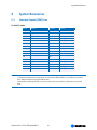
1
Kontron User's Guide COMe-bCD2 Document Revision 120 This page intentionally left blank Table of Contents Table of Contents 1 User Information ........................................................................................................ 6 1.1 1.2 1.3 1.4 1.5 1.6 2 Introduction .............................................................................................................. 8 2.1 2.2 2.2.1 2.2.2 2.3 2.4 2.5 2.6 3 COMe-bCD2 ......................................................................................................8 COMe-bCD2 Release Versions ...............................................................................9 Single Channel Version .......................................................................................9 Dual Channel Version .........................................................................................9 COMe-bCD2 Module Overview ...............................................................................9 Understanding COM Express® functionality .......................................................... 11 COM Express® Documentation ........................................................................... 11 COM Express® Benefits ..................................................................................... 12 Specifications ...........................................................................................................13 3.1 3.1.1 3.2 3.3 3.3.1 3.4 3.4.1 3.4.2 3.5 4 About This Manual .............................................................................................6 Copyright Notice ...............................................................................................6 Trademarks ......................................................................................................6 Standards ........................................................................................................6 Warranty .........................................................................................................6 Technical Support..............................................................................................7 Functional Specifications .................................................................................. 13 Block diagram ................................................................................................ 16 Mechanical Specifications ................................................................................. 17 Electrical Specifications .................................................................................... 17 Power Consumption ......................................................................................... 17 Environmental Specifications ............................................................................ 18 Temperature................................................................................................... 18 Humidity ....................................................................................................... 18 MTBF............................................................................................................. 18 Connector Pinouts .....................................................................................................19 4.1 4.2 4.2.1 4.2.2 4.3 4.3.1 4.3.2 4.3.3 4.3.4 4.3.5 Connector location .......................................................................................... 19 Pinout tables .................................................................................................. 20 Connector X1A ................................................................................................ 21 Connector X1B ................................................................................................ 25 Signal description ........................................................................................... 29 PCIexpress x1 lanes ......................................................................................... 29 USB .............................................................................................................. 29 SATA ............................................................................................................. 29 Audio ............................................................................................................ 29 Serial IRQ ...................................................................................................... 29 Kontron User's Guide ETXexpress® CD iii Table of Contents 4.3.6 4.3.7 4.3.8 4.3.9 4.3.10 4.3.11 4.3.12 4.3.13 4.3.14 4.3.15 4.3.16 5 Special Features ........................................................................................................34 5.1 5.2 6 Thermal Management ....................................................................................... 36 COMe-bCD2 onboard Fan connector..................................................................... 37 Location and pinout of fan connector J4 .............................................................. 38 BIOS settings for fan control ............................................................................. 39 Electrical Characteristics ................................................................................... 39 Important Technology Information ..............................................................................41 8.1 8.1.1 8.1.2 8.1.3 8.2 8.2.1 8.3 8.4 9 Cooling Solutions ............................................................................................ 35 Design Considerations................................................................................................36 7.1 7.2 7.2.1 7.2.2 7.2.3 8 Watchdog Timer .............................................................................................. 34 General Purpose Input and Output ...................................................................... 34 Important Information...............................................................................................35 6.1 7 VGA Output .................................................................................................... 29 LVDS Flat Panel Interface (JILI).......................................................................... 30 Digital Flat Panel Interface (JIDI) ....................................................................... 30 Ethernet ........................................................................................................ 30 Power Control ................................................................................................. 31 Power Management ......................................................................................... 31 Miscellaneous Circuits ...................................................................................... 31 PCIexpress Graphics ......................................................................................... 32 PCI Bus.......................................................................................................... 32 IDE Port......................................................................................................... 32 SDVO Output................................................................................................... 32 I/O APIC mode ................................................................................................ 41 Method of interrupts transmission ...................................................................... 41 Interrupt priority ............................................................................................ 41 More interrupts ............................................................................................... 41 Thermal Monitor and Catastrophic Thermal Protection ............................................ 41 Summary ....................................................................................................... 42 Processor Performance Control .......................................................................... 42 Thermal Management ....................................................................................... 43 System Ressources ....................................................................................................44 9.1 9.2 9.3 9.4 9.5 Interrupt Request (IRQ) Lines ............................................................................ 44 Direct Memory Access (DMA) Channels ................................................................. 45 Memory Area .................................................................................................. 46 I/O Address Map ............................................................................................. 46 Peripheeral Component Interconnect (PCI) Devices ................................................ 46 Kontron User's Guide ETXexpress® CD iv Table of Contents 9.6 9.7 9.8 10 Inter IC (I2C) Bus ............................................................................................. 46 System Managment (SM) Bus ............................................................................. 47 JILI I2C Bus .................................................................................................... 47 BIOS Operation..........................................................................................................48 10.1 Determining the BIOS Version ............................................................................ 48 10.2 Setup Guide ................................................................................................... 48 10.2.1 Start Phoenix BIOS Setup Utility ......................................................................... 48 11 BIOS Setup ...............................................................................................................50 11.1 Info Screen .................................................................................................... 50 11.2 Main Menu ..................................................................................................... 50 11.2.1 IDE Channels Submenu ..................................................................................... 51 11.3 Advanced....................................................................................................... 52 11.3.1 Keyboard Features Submenu .............................................................................. 53 11.3.2 Cache Memory Submenu ................................................................................... 54 11.3.3 Hardware Monitor Submenu .............................................................................. 56 11.3.4 Watchdog Settings Submenu ............................................................................. 57 11.3.5 Miscellaneous Submenu.................................................................................... 58 11.3.6 Console Redirection Submenu ............................................................................ 59 11.4 Devices ......................................................................................................... 60 11.4.1 CPU Control .................................................................................................... 61 11.5 Chipset Control ............................................................................................... 65 11.6 Integrated Video ............................................................................................. 67 11.6.1 Display Control ............................................................................................... 68 11.7 Chipset Integrated Devices ................................................................................ 68 11.7.1 PCI Express Ports ............................................................................................. 70 11.7.2 PCI/PNP ISA IRQ Ressource Exclusion .................................................................. 71 11.7.3 USB Ports ...................................................................................................... 72 11.8 LAN Options ................................................................................................... 73 11.9 SIO Options .................................................................................................... 74 11.10 Security......................................................................................................... 76 11.11 Power ........................................................................................................... 77 11.11.1 ACPI Parameter Control .................................................................................... 78 11.12 Boot ............................................................................................................. 79 11.13 Exit .............................................................................................................. 80 Kontron User's Guide ETXexpress® CD v 1 User Information 1 User Information 1.1 About This Manual This document provides information about products from Kontron Embedded Modules GmbH and/or its subsidiaries. No warranty of suitability, purpose, or fitness is implied. While every attempt has been made to ensure that the information in this document is accurate, the information contained within is supplied “as-is” and is subject to change without notice. For the circuits, descriptions and tables indicated, Kontron assumes no responsibility as far as patents or other rights of third parties are concerned. 1.2 Copyright Notice Copyright © 2003-20012 Kontron Embedded Modules GmbH All rights reserved. No part of this document may be reproduced, transmitted, transcribed, stored in a retrieval system, or translated into any language or computer language, in any form or by any means (electronic, mechanical, photocopying, recording, or otherwise), without the express written permission of Kontron Embedded Modules GmbH. DIMM-PC®, PISA®, ETX®, COM Express® , X-board®, DIMM-IO® and DIMM-BUS® are trademarks or registered trademarks of Kontron Embedded Modules GmbH. Kontron is trademark or registered trademark of Kontron AG. 1.3 Trademarks The following lists the trademarks of components used in this board. IBM, XT, AT, PS/2 and Personal System/2 are trademarks of International Business Machines Corp. Microsoft is a registered trademark of Microsoft Corp. Intel is a registered trademark of Intel Corp. All other products and trademarks mentioned in this manual are trademarks of their respective owners. 1.4 Standards Kontron Embedded Modules GmbH is certified to ISO 9000 standards. 1.5 Warranty This Kontron Embedded Modules GmbH product is warranted against defects in material and workmanship for the warranty period from the date of shipment. During the warranty period, Kontron Embedded Modules GmbH will at its discretion decide to repair or replace defective products. Within the warranty period, the repair of products is free of charge as long as warranty conditions are observed. Kontron User's Guide ETXexpress® CD 6 1 User Information The warranty does not apply to defects resulting from improper or inadequate maintenance or handling by the buyer, unauthorized modification or misuse, operation outside of the product‟s environmental specifications or improper installation or maintenance. Kontron Embedded Modules GmbH will not be responsible for any defects or damages to other products not supplied by Kontron Embedded Modules GmbH that are caused by a faulty Kontron Embedded Modules GmbH product. 1.6 Technical Support Technicians and engineers from Kontron Embedded Modules GmbH and/or its subsidiaries are available for technical support. We are committed to making our product easy to use and will help you use our products in your systems. Please consult our Web site at http://www.kontron.com/support for the latest product documentation, utilities, drivers and support contacts. Consult our customer section http://emdcustomersection.kontron.com for the latest BIOS downloads, Product Change Notifications and additional tools and software. In any case you can always contact your board supplier for technical support. Kontron User's Guide ETXexpress® CD 7 2 Introduction 2 Introduction 2.1 COMe-bCD2 Based on the COM Express standard, Kontron‟s COMe-bCD2, powered by a variety of Intel Pentium core duo processors, is a next-generation embedded module that brings advanced technology to tomorrow‟s applications, as well as continuing today‟s legacy devices. Built around serial differential signaling technologies, COMe-bCD2 modules incorporate the following interfaces into a 95 x 125 small form factor embedded module: Core 2 Duo / Core Duo / Celeron M PCI Express, which provides a high performance I/O infrastructure with transfer rates starting at 2.5 Giga transfers per second over a x1 PCI Express lane PCI Serial ATA (SATA II) USB 2.0 LVDS Intel High Definition Audio Advanced Configuration and Power Interface (ACPI) for optimized power management The COMe-bCD2 is built around the Intel Core Duo processors that use the Yonah and Merom Cores and the Mobile Intel 945GME Express chipset, which is the first mobile platform to offer PCI Express functionality with extended life cycle support. These modules feature the most current desktop features such as USB 2.0, SATA, and PCI Express buses. The COMe-bCD2 delivers up to 2GHz performance and up to 2GB DDR2 RAM. For applications that require advanced real-time video capabilities, the COMe-bCD2 has integrated graphics based on the Intel® Graphics Media Accelerator 900 architecture and also supports PCI Express graphics. Fast communications are possible courtesy of a Gigabit Ethernet port. The COMe-bCD2 supports 5 PCI Express x1 Lanes and PCI Express cards as well as established hardware solutions based on current buses such as 32-bit PCI. A Gigabit Ethernet port provides fast connectivity to LAN/WAN and 8 USB 2.0 ports provide fast and sufficient interfaces for external peripherals. COMe-bCD2 modules also provide the following interfaces that are always located in the same physical position on each board: PCI-express, PCI32, USB, serial ATA (SATA), parallel ATA (PATA), LVDS Multi Media ports, as well as an ACPI (Advanced Configuration and Power Interface) for optimized power management. Six mounting holes on the board provide secure mounting to allow the module increased shock and vibration resistance. Kontron User's Guide ETXexpress® CD 8 2 Introduction 2.2 COMe-bCD2 Release Versions The COMe-bCD2 module is available in two different versions. The single channel version has one memory socket and the dual channel verison has two memory sockets. All statements in this document are valid for both versions, except they market to be only valid for one version. Statements only valid for the single channel version are highlighted in a light blue color and statements only valid for the dual channel version are highlighted in a green color. The main differences are: 2.2.1 Single Channel Version Article number ends with a “-0”, “-1”, “-2” or “-3” One memory socket 5 PCIexpress lanes of the chipset; Onboard LAN uses PCIexpress lane 1 No S3 cold support Strict 12V supply voltage Intel® 945GM Ethernetcontroller: Realtec RTL8111B Temperature sensor: LM 64 2.2.2 Dual Channel Version Article number ends with a “-4”, “-5” or “-6” Two memory sockets 5PCIexpress lanes of the chipset; Onboard LAN uses PCIexpress lane 5 which allows optionally a x4 lane S3 cold support Wide Range power input from 8.5V to 18V Intel® 945GME Ethernetcontroller: Realtec RTL8111C Temperature sensor: LM 87 2.3 COMe-bCD2 Module Overview The international COM Express standard defines two new form factor sizes: Basic and Extended. The primary difference between the Basic and Extended size is a larger board size and thermal envelope in the Extended size. The COMe-bCD2 follows the basic form factor. Five module Pin-out Type definitions exist for Basic and Extended modules. Pin-out Types 1-5 apply to Basic and Extended module form factors. Pin-out Types 1-5 offer different functionalities. For a complete explanation of the features of each of the Pin-out Types 1-5, please see the COM Express® Specification. Kontron User's Guide ETXexpress® CD 9 2 Introduction The COMe-bCD2 uses the Pin-out Type 2 architecture, which includes PCI and IDE interfaces. These modules either use onboard graphics capabilities or may use 16 PEG lanes to connect to an external video controller. In case of onboard graphics, PEG pins may be alternatively used for two SDVO ports. Pin-out Type 2 features include: Dual 220 pin connectors (Primary Connector: Rows A-B and Secondary Connector: Rows C-D, 440 pins total) 32-bit PCI interface IDE port (to support legacy ATA devices) Up to 5 PCI Express general purpose lanes One, x16 PCI Express Graphics (PEG) slot SDVO option (pins shared with PCI Express Graphics) Maximum module input power capability extended to 188W Up to 8 USB 2.0 ports; 4 shared over-current lines Up to 4 Serial ATA or SAS ports Dual 24-bit LVDS channels Analog VGA and TV Out: Composite Video, S-Video, Component Video (YPbPr) Intel High Definition Audio (Azalia) and AC '97 digital audio interface (external CODEC) Single Ethernet interface with integrated PHY +12V primary power supply input, +5V standby and 3.3V RTC power supplies Kontron User's Guide ETXexpress® CD 10 2 Introduction 2.4 Understanding COM Express® functionality All Kontron COM Express® basic and compact modules contain two connectors, each of which has two rows. The primary connector has two rows called Row A and Row B. The secondary connector has two rows called Row C and Row D. The primary connector (Row A and Row B) feature the following legacy-free functionality: Ethernet Serial ATA (SATA) USB 2.0 LVDS/VGA and dual display video Intel High Definition Audio (Azalia) LPC, an Intel proprietary low-pin count (LPC), which supports low-speed devices such as RS-232 serial and parallel ports. The secondary connector (Row C and Row D) provides support for the following buses and I/O: PCI Express PCI IDE 2.5 COM Express® Documentation This product manual serves as one of three principal references for an COM Express® design. It documents the specifications and features of COMe-bCD2. The other two references, which are available from your Kontron Support, include: The COMexpress Specification define the module form factor, pinout, and signals. The Carrier Board Design Guide serves as a general guide for baseboard design, with a focus on maximum flexibility to accommodate a wide range of COM Express® modules. Note: Some of the information contained within this product manual applies only to certain product revisions (CE: xxx). If certain information applies to specific product revisions (CE: xxx) it will be stated. Please check the product revision of your module to see if this information is applicable. Kontron User's Guide ETXexpress® CD 11 2 Introduction 2.6 COM Express® Benefits COM Express® basic modules are very compact (125 x 95 mm, 12mm thick), highly integrated computers. All COM Express® modules feature a standardized form factor and a standardized connector layout that carry a specified set of signals. Each COM Express® module is based on connector type of the COMexpress specification. This standardization allows designers to create a single-system baseboard that can accept present and future COM Express® modules. COM Express® modules include common personal computer (PC) peripheral functions such as: Graphics USB ports Ethernet Sound IDE (and SATA) The baseboard designer can optimize exactly how each of these functions implements physically. Designers can place connectors precisely where needed for the application on a baseboard designed to optimally fit a system‟s packaging. A peripheral PCI bus can be implemented directly on the baseboard rather than on mechanically unwieldy expansion cards. The ability to build a system on a single baseboard using the computer as one plug-in component simplifies packaging, eliminates cabling, and significantly reduces system-level cost. A single baseboard design can use a range of COM Express® modules. This flexibility can differentiate products at various price/performance points, or to design future proof systems that have a built-in upgrade path. The modularity of an COM Express® solution also ensures against obsolescence as computer technology evolves. A properly designed COM Express® baseboard can work with several successive generations of COM Express® modules. An COM Express® baseboard design has many advantages of a custom, computer-board design but delivers better obsolescence protection, greatly reduced engineering effort, and faster time to market. Kontron User's Guide ETXexpress® CD 12 3 Specifications 3 Specifications 3.1 Functional Specifications Processor Intel® Celeron® M, Core Duo® (Yonah Core)or Core2Duo® (Merom core) processor Bus 533 / 667 MHz CPU bus 533/667 MHz memory bus Chipset Intel® 945GM (see 2.2.1) Intel® 945GME (see 2.2.2) ICH7M-DH Cache, Second level 1MB (Celeron® M) 2x1MB (Core Duo®) 4MB (Core2Duo®) Memory One 200-pin DDR2-SO-DIMM (-533 or -667) (see 2.2.1) Two 200-pin DDR2-SO-DIMM (-533 or -677) (see 2.2.2) Note: COMe-bCD2 equipped with the CeleronM423 is not able to drive memory modules faster than DDR2-533. Note: The dual channel version would be theoretically able to support 4GB of RAM. Practically this feature is in the chipset not supported, therefore that maximum amount of RAM is about 3.3 GByte PCI Express Graphics (PEG): Intel® 945GM/GME One 16-lane PCI Express port for external PCI Express based graphics card Serial Digital Video Output (SDVO): Intel® 945GM/GME Concurrent Operation of PCI Express Graphics with SDVO Supports appropriate external SDVO compontents (DVI, LVDS, TV-out) Kontron User's Guide ETXexpress® CD 13 3 Specifications PCI Express: Intel® ICH7M-DH 5 PCI Express x1 lanes Optionally 1 x4 lane and 1 x1 lane is possible by strapping option on the baseboard. (see 2.2.2) To use this feature please pull-up AC_SYNC (A29) and AC_SDOUT (A33) to 3.3V. PCI 32: Intel® ICH7M-DH Parallel PCI Bus 32 bit 33 MHz Low Pincount Bus (LPC): Intel® ICH7M-DH Enhanced Intelligent Drive Electronics (EIDE): Intel® ICH7M-DH One PCI Bus Master IDE port Supports 2 IDE devices Ultra 100 Direct Memory Access (DMA) mode Programmed Input/Output (PIO) modes up to Mode 4 timing Multiword DMA Mode 0,1,2 with independent timing Serial ATA: Intel® ICH7M-DH 2 Channels Serial ATA SATA Spec. Rev. 1.0 up to 150 MB/s per channel SATA II (AHCI) Supports RAID level 0 and 1 Universal Serial Bus: Intel® ICH7M-DH 8 USB 1.1/2.0 ports (UHCI and EHCI) USB legacy keyboard support USB floppy, CD-ROM, Hard drive, and memory stick boot support Gigabit Ethernet: Realtek RTL8111B/C 10/100/1000 Fully compatible with IEEE 802.3, IEEE 802.3u, IEEE 802.3ab Onboard video graphics array (VGA): Intel® 945GM/GME: Intel® Gen 3.5 Graphics engine Dynamic Video Memory Technology (DVMT 3.0) Cathode ray tube (CRT) up do QXGA low voltage differential signaling (LVDS) liquid-crystal display (LCD) and SDVO interfaces up to UXGA Supports DX 9.1 Kontron User's Guide ETXexpress® CD 14 3 Specifications AC ’97 (Audio): Intel® 945GM/GME; Up to 20 bit sample resolution Multiple sample rates up to 48bit Independent bus master logic for dual Microphone Input, dual PCM audio input, PCM audio input, modem input, modem output and S/PDIF output. Television output: Intel® 945GM/GME 3 integrated 10bit DACs Overscaling NTSC/PAL HDTV support: 480p / 780p / 1080i / 1080p BIOS: Phoenix, 1MB Flash-BIOS in Firmware Hub Flash Memory NV-EEPROM for CMOS-setup retention without battery Watchdog timer (WDT): Xilinx Microcontroller Real-time clock (requires external battery) Kontron User's Guide ETXexpress® CD 15 3 Specifications 3.1.1 ETXexpress-CD Block diagram CPU Celeron M Core Duo Core 2 Duo Host Bus North Bridge DDR2SDRAM Intel 945GM VGA Controller LCD (JILI) Hub Interface TV out IDE RTC USB 0-7 South Bridge PCIe 1-5 Connector AB PEG PCI BUS Intel ICH7MDH SATA 0-1 AC’97 SPI Sound PCIe LPC BUS MISC Power Control Speaker Battery SMB I2C TPM (optional) Realtek RTL8111 Gigabit Ethernet Kontron User's Guide ETXexpress® CD 16 BIOS Connector CD CRT 3 Specifications 3.2 Mechanical Specifications Dimensions 95.0 mm x 125.0 mm Height approx. 12 mm (0.4”) 3.3 Electrical Specifications Supply Voltage 12V DC +/- 5% 8.5V DC to 18V DC widerange input (see 2.2.2) Supply Voltage Ripple Maximum 100 mV peak to peak 0 – 20 MHz Supply Current 5 V_SB Note: 3.3.1 0,33 A in S5 mode 0,43 A in S0 S3 cold will drive all the powersupply for memory refreshing and chip supply through the 5V_SB line. Therefore up to 2A of current is specified for the connectors and should be in mind when the powersupply is dimenstioned. The board works also without a 5V_SB line but not the ACPI states S3 and S5. Power Consumption The maximum Power Consumption of the different COMe-bCD2 modules is between 18 - 40W (100% CPU load; 90°C CPU temperature). Further details with measurements and TDP values of the single variants can be found in our customer section. Information there is available after registration. All boards were equipped with DDR2 SDRAM. The Modules were tested using maximum CPU frequency. Kontron User's Guide ETXexpress® CD 17 3 Specifications 3.4 Environmental Specifications 3.4.1 Temperature Operating: (with Kontron Embedded Modules heat-spreader plate assembly): Ambient temperature: 0°C to 60°C Maximum heatspreader-plate temperature: 0°C to 60°C Non-operating: -30°C to 85°C Note: The maximum operating temperature with the heatspreader plate is the maximum measurable temperature on any spot on the heatspreader’s surface. You must maintain the temperature according to the above specification. Operating (without Kontron Embedded Modules heat-spreader plate assembly): Maximum operating temperature: 0°C to 60°C Non operating: -30 to +85 °C Note: 3.4.2 The maximum operating temperature is the maximum measurable temperature on any spot on a module’s surface. You must maintain the temperature according to the above specification. Humidity Operating: 10% to 90% (non condensing) Non operating: 5% to 95% (non condensing) 3.5 MTBF The following MTBF (Mean Time Between Failure) values were calculated using a combination of manufacturer‟s test data, if the data was available, and a Bellcore calculation for the remaining parts. The Bellcore calculation used is “Method 1 Case 1”. In that particular method the components are assumed to be operating at a 50 % stress level in a 40° C ambient environment and the system is assumed to have not been burned in. Manufacturer‟s data has been used wherever possible. The manufacturer‟s data, when used, is specified at 50° C, so in that sense the following results are slightly conservative. The MTBF values shown below are for a 40° C in an office or telecommunications environment. Higher temperatures and other environmental stresses (extreme altitude, vibration, salt water exposure, etc.) lower MTBF values. Notes: System MTBF (hours) for single channel memory version: 152941 System MTBF (hours) for dual channel memory version: 191206 Fans usually shipped with Kontron Embedded Modules GmbH products have 50,000-hour typical operating life. The above estimates assume no fan, but a passive heat sinking arrangement. Estimated RTC battery life (as opposed to battery failures) is not accounted for in the above figures and need to be considered for separately. Battery life depends on both temperature and operating conditions. When the Kontron unit has external power; the only battery drain is from leakage paths. Kontron User's Guide ETXexpress® CD 18 4 Connector Pinouts 4 Connector Pinouts 4.1 Connector location There are 2 connectors on the basic sized module. Connector X1A and Connector X1B are shown in the following drawing. It is a top layer view and the connectors are seen "through" the PCB. Each connector consist s of 2 connector rows. Connector X1A has rows A and B and connector X1B has rows C and D. Pin D1 Pin C1 Pin B1 Pin A1 Connector X1B Connector X1A Kontron User's Guide ETXexpress® CD 19 4 Connector Pinouts 4.2 Pinout tables Type I IO-2,5 IO-3,3 IO-5 I-3,3 I-5 O OA O-2,5 O-3,3 O-5 DP PU PD PWR Nc Notes: Signal Description Differential Pair Input Bi-directional 2,5 V IO-Signal Bi-directional 3,3 V IO-Signal Bi-directional 5 V IO-Signal 3,3 V Input 5 V Input Differential Pair Output Output Analog 2,5 V Output 3,3 V Output 5 V Output Differential Pair Input/Output Pull-Up Resistor Pull-Down Resistor Power Connection Not Connected / Reserved To protect external power lines of peripheral devices, make sure that: the wires have the right diameter to withstand the maximum available current the enclosure of the peripheral device fulfils the fire-protection requirements of IEC/EN60950 Kontron User's Guide ETXexpress® CD 20 4 Connector Pinouts 4.2.1 Connector X1A Connector X1A (Signal Levels A1-A55) Pin A1-A55 Pin Signal A1 A2 A3 A4 A5 A6 A7 A8 A9 A10 A11 A12 A13 A14 A15 A16 A17 A18 A19 A20 A21 A22 A23 A24 A25 A26 A27 A28 A29 A30 A31 A32 A33 A34 A35 A36 A37 A38 A39 A40 A41 A42 A43 A44 A45 A46 A47 A48 A49 A50 A51 A52 A53 A54 A55 Note: GND GBE0_MDI3GBE0_MDI3+ GBE0_LINK100# GBE0_LINK1000# GBE0_MDI2GBE0_MDI2+ GBE0_LINK# GBE0_MDI1GBE0_MDI1+ GND GBE0_MDI0GBE0_MDI0+ GBE0_CTREF SUS_S3# SATA0_TX+ SATA0_TXSUS_S4# SATA0_RX+ SATA0_RXGND SATA2_TX+ SATA2_TXSUS_S5# SATA2_RX+ SATA2_RXBATLOW# ATA_ACT# AC_SYNC AC_RST# GND AC_BITCLK AC_SDOUT BIOS_DISABLE# THRMTRIP# USB6USB6+ USB_6_7_OC# USB4USB4+ GND USB2USB2+ USB_2_3_OC# USB0USB0+ VCC_RTC EXCD0_PERST# EXCD0_CPPE# LPC_SERIRQ GND PCIE_TX5+ PCIE_TX5GPI0 PCIE_TX4+ [ LAN | Power | USB | SATA | PCIe | AUDIO] Type Termination Comment Description Power Ground LAN_RXD- | Ethernet Receive Data LAN_RXD- | Ethernet Receive Data LAN_100LED# | Ethernet Speed LED LAN_1000LED# | Ethernet Speed LED LAN_RXD- | Ethernet Receive Data LAN_RXD- | Ethernet Receive Data LAN_LILED# | LAN Link LED LAN_RXD- | Ethernet Receive Data LAN_RXD+ | Ethernet Receive Data + Power Ground LAN_TXD- | Ethernet Transmit Data LAN_TXD+ | Ethernet Transmit Data + ETH_CTREF PM_SLP_S#3 SATA0_TX+ | SATA 0 Transmit Data + SATA0_TX- | SATA 0 Transmit Data PM_SLP_S#4 SATA0_RX+ | SATA 0 Receive Data + SATA0_RX- | SATA 0 Receive Data Power Ground SATA0_TX+ | SATA 2 Transmit Data + SATA0_TX- | SATA 2 Transmit Data PM_SLP_S#5 SATA0_RX+ | SATA 2 Receive Data + SATA0_RX- | SATA 2 Receive Data PM_BATLOW# | Battery Low ATA_LED# | SATA LED AC_SYNC | AC'97 Sync AC_RST# | AC'97 Reset Power Ground AC_BITCLK | AC'97 Clock AC_SDATAOUT | AC'97 Data BIOS_DISABLE# PM_THRMTRIP#_CON USB_PN6 | USB Data – Port6 USB_PP6 | USB Data + Port6 USB_OC#_6_7 | USB OverCurrent Port 6/7 USB_PN4 | USB Data - Port4 USB_PP4 | USB Data + Port4 Power Ground USB_PN2 | USB Data - Port2 USB_PP2 | USB Data + Port2 USB_OC#_2_3 | USB OverCurrent Port 2/3 USB_PN0 | USB Data - Port0 USB_PP0 | USB Data + Port0 +V_BAT Express Card Support [0]|card reset Express Card Support [0]| capable c. request INT_SERIRQ | Serial Interrupt Request Power Ground n.c. n.c. GPI0 | General Purpose Input 0 PCI Express lane 4 + Transmit PWR I I O-3,3 O-3,3 I I O-3,3 I I PWR O O O-3,3 O-3,3 O O O-3,3 I I PWR O O O-3,3 O O I-3,3 O-3,3 O-3.3 O-3,3 PWR I-3,3 O-3,3 I-3,3 IO-3,3 DP DP I-3,3 DP DP PWR DP DP I-3,3 DP DP PWR O-3,3 I-3,3 IO-3,3 PWR Nc Nc I-3,3 O PU 8k2 3,3V PU 10k 3,3V PU 10k 3,3V PU 10k 3,3V PU 8k2 3,3V PU 10k 3,3V - On at 100Mb/s On at 1000Mb/s int. PD 20k in ICH7–PU to 3.3V f. x4 int. PD 20k in ICH7 int. PD 20k in ICH7 int. PD 20k in ICH7–PU to 3.3V f. x4 int. PD 15k in ICH7 int. PD 15k in ICH7 int. PD 15k in ICH7 int. PD 15k in ICH7 int. PD 15k in ICH7 int. PD 15k in ICH7 int. PD 15k in ICH7 int. PD 15k in ICH7 - The termination resistors in this table are already mounted on the COM Express® board. Refer to the design guide for information about additional termination resistors. Kontron User's Guide ETXexpress® CD 21 4 Connector Pinouts Connector X1A (Signal Levels A56-A110) Pin A56-A110 Pin Signal A56 A57 A58 A59 A60 A61 A62 A63 A64 A65 A66 A67 A68 A69 A70 A71 A72 A73 A74 A75 A76 A77 A78 A79 A80 A81 A82 A83 A84 A85 A86 A87 A88 A89 A90 A91 A92 A93 A94 A95 A96 A97 A98 A99 A100 A101 A102 A103 A104 A105 A106 A107 A108 A109 A110 Note: PCIE_TX4GND PCIE_TX3+ PCIE_TX3GND PCIE_TX2+ PCIE_TX2GPI1 PCIE_TX1+ PCIE_TX1GND GPI2 PCIE_TX0+ PCIE_TX0GND LVDS_A0+ LVDS_A0LVDS_A1+ LVDS_A1LVDS_A2+ LVDS_A2LVDS_VDD_EN LVDS_A3+ LVDS_A3GND LVDS_A_CK+ LVDS_A_CKLVDS_I2C_CK LVDS_I2C_DAT GPI3 KBD_RST# KBD_A20GATE PCIE0_CK_REF+ PCIE0_CK_REFGND RSVD RSVD GPO0 RSVD RSVD GND VCC_12V VCC_12V VCC_12V GND VCC_12V VCC_12V VCC_12V VCC_12V VCC_12V VCC_12V VCC_12V VCC_12V VCC_12V GND Description Type PCI Express lane 4 Power Ground PCI Express lane 3 + PCI Express lane 3 Power Ground PCI Express lane 2 + PCI Express lane 2 GPI1 | General Purpose Input 1 PCI Express lane 1 + PCI Express lane 1 Power Ground GPI2 | General Purpose Input 2 PCI Express lane 0 + PCI Express lane 0 Power Ground LVDS_YAP0 | LVDS Channel A Data0+ LVDS_YAM0 | LVDS Channel A Data0LVDS_YAP1 | LVDS Channel A Data1+ LVDS_YAM1 | LVDS Channel A Data1LVDS_YAP2 | LVDS Channel A Data2+ LVDS_YAM2 | LVDS Channel A Data2 LVDS_VDDEN | LVDS Panel Power Control LVDS_YAP3 | LVDS Channel A Data3+ LVDS_YAM3 | LVDS Channel A Data3Power Ground LVDS_CLKAP | LVDS Channel A Clock+ LVDS_CLKAM | LVDS Channel A ClockLVDS_DDCPCLK | JILI I2C Clock LVDS_DDCPDATA | JILI I2C Data GPI3 | General Purpose Input 3 H_RCIN# | Keyboard Reset H_A20GATE CLK_PCIE_REF P CLK_PCIE_REF P Power Ground n.c. n.c. GPO0 | General Purpose Output 0 n.c. n.c. Power Ground 12V VCC 12V VCC 12V VCC Power Ground 12V VCC 12V VCC 12V VCC 12V VCC 12V VCC 12V VCC 12V VCC 12V VCC 12V VCC Power Ground O PWR O O PWR O O I-3,3 O O PWR I-3,3 O O PWR O O O O O O O-2,5 O O PWR O O IO-3,3 IO-3,3 I-3,3 I-3,3 I-3,3 O O PWR Nc Nc O-3,3 Nc Nc PWR PWR PWR PWR PWR PWR PWR PWR PWR PWR PWR PWR PWR PWR PWR Termination PU 10k 3,3V PU 10k 3,3V PU 4k7 3,3V PU 4k7 3,3V PU 10k 3,3V PU 10k 3,3V PU 10k 3,3V PD 10k - [ Power | LVDS | PCIe ] Comment - The termination resistors in this table are already mounted on the COM Express® board. Refer to the design guide for information about additional termination resistors. Kontron User's Guide ETXexpress® CD 22 4 Connector Pinouts Connector X1B (Signal Levels B1-B55) Pin B1-B55 Pin Signal B1 B2 B3 B4 B5 B6 B7 B8 B9 B10 B11 B12 B13 B14 B15 B16 B17 B18 B19 B20 B21 B22 B23 B24 B25 B26 B27 B28 B29 B30 B31 B32 B33 B34 B35 B36 B37 B38 B39 B40 B41 B42 B43 B44 B45 B46 B47 B48 B49 B50 B51 B52 B53 B54 B55 Note: GND GBE0_ACT LPC_FRAME# LPC_AD0 LPC_AD1 LPC_AD2 LPC_AD3 LPC_DRQ0# LPC_DRQ1# LPC_CLK GND PWRBTN# SMB_CK SMB_DAT SMB_ALERT# SATA1_TX+ SATA1_TXSUS_STAT# SATA1_RX+ SATA1_RXGND SATA3_TX+ SATA3_TXPWR_OK SATA3_RX+ SATA3_RXWDT AC_SDIN2 AC_SDIN1 AC_SDIN0 GND SPKR I2C_CK I2C_DAT THRM# USB7USB7+ USB_4_5_OC# USB5USB5+ GND USB3USB3+ USB_0_1_OC# USB1USB1+ EXCD1_PERST# EXCD1_CPPE# SYS_RESET# CB_RESET# GND PCIE_RX5+ PCIE_RX5GPO1 PCIE_RX4+ [ LAN | Power | USB | SATA | PCIe | AUDIO | LPC] Type Termination Comment Description Power Ground LAN_ACTLED# | Ethernet Activity LED LPC_FRAME# | LPC Frame Indicator LPC_AD0 | LPC Adress & DATA Bus LPC_AD1 | LPC Adress & DATA Bus LPC_AD2 | LPC Adress & DATA Bus LPC_AD3 | LPC Adress & DATA Bus SIO_DRQ#0 | LPC Request 0 SIO_DRQ#1 | LPC Request 1 CLK_SIOEXTPCI Power Ground Power Button SMB_CLK | SMBUS Clock SMB_DATA | SMBUS Data SMB_ALERT# SATA1_TX+ SATA1_TXPM_SUS_ STAT# SATA1_RX+ SATA1_RXPower Ground SATA3_TX+ SATA3_TXETX_PWR_OK | Power OK SATA3_RX+ SATA3_RXWatch Dog Timer AC_SDATAIN2 | AC'97 Serial Input Data 2 AC_SDATAIN1 | AC'97 Serial Input Data 1 AC_SDATAIN0 | AC'97 Serial Input Data 0 Power Ground AC_SPKR | Speaker I2CLK I2DAT PM THRM# CON | Over Temperature USB_PN7 | USB Data – Port7 USB_PP7 | USB Data + Port7 USB_OC#_4_5 | USB OverCurrent Port 4/5 USB_PN5 | USB Data- Port5 USB_PP5 | USB Data+ Port5 Power Ground USB_PN3 | USB Data- Port3 USB_PP3 | USB Data+ Port3 USB_OC#_0_1 | USB OverCurrent Port 0/1 USB_PN1 | USB Data- Port1 USB_PP1 | USB Data+ Port1 Express Card Support [1]|card reset Express Card Support [1]| capable c. ETX_SYS_RESET# | Reset Input request PCI_RST# | PCI Bus Reset Power Ground n.c. n.c. GPO1 | General Purpose Output 1 PCI Express lane 4 + Recieve PWR O-3,3 I-3,3 IO-3,3 IO-3,3 IO-3,3 IO-3,3 I-3,3 I-3,3 O-3,3 PWR I-5 O-3,3 IO-3,3 IO-3,3 O O O-3,3 I I PWR O O I-3,3 I I O-3,3 I-3,3 I-3,3 I-3,3 PWR O-3,3 O-3,3 IO-3,3 O-3,3 DP DP I-3.3 DP DP PWR DP DP I-3.3 DP DP O-3,3 I-3,3 I-3,3 O-3,3 PWR Nc Nc O-3,3 I PU 2k2 3,3V PU 2k2 3,3V PU 2k2 3,3V PU 2k2 3,3V PU 2k2 3,3V PU 10k 3,3V PU 10k 3,3V PU 10k 3,3V PU 10k 3,3V PD 10k - int. PD 20k in ICH7 int. PD 20k in ICH7 int. PD 20k in ICH7 int. PD 20k in ICH7 int. PD 15k in ICH7 int. PD 15k in ICH7 int. PD 15k in ICH7 int. PD 15k in ICH7 int. PD 15k in ICH7 int. PD 15k in ICH7 int. PD 15k in ICH7 int. PD 15k in ICH7 availlable when ICH7-MDH or -R The termination resistors in this table are already mounted on the COM Express® board. Refer to the design guide for information about additional termination resistors. Kontron User's Guide ETXexpress® CD 23 4 Connector Pinouts Connector X1A (Signal Levels B56-B110) Pin B56-B110 Pin Signal B56 B57 B58 B59 B60 B61 B62 B63 B64 B65 B66 B67 B68 B69 B70 B71 B72 B73 B74 B75 B76 B77 B78 B79 B80 B81 B82 B83 B84 B85 B86 B87 B88 B89 B90 B91 B92 B93 B94 B95 B96 B97 B98 B99 B100 B101 B102 B103 B104 B105 B106 B107 B108 B109 B110 Note: PCIE_RX4GPO2 PCIE_RX3+ PCIE_RX3GND PCIE_RX2+ PCIE_RX2GPO3 PCIE_RX1+ PCIE_RX1WAKE0# WAKE1# PCIE_RX0+ PCIE_RX0GND LVDS_B0+ LVDS_B0LVDS_B1+ LVDS_B1LVDS_B2+ LVDS_B2LVDS_B3+ LVDS_B3LVDS_BKLT_EN GND LVDS_B_CK+ LVDS_B_CKLVDS_BKLT_CTRL VCC_5V_SBY VCC_5V_SBY VCC_5V_SBY VCC_5V_SBY RSVD VGA_RED GND VGA_GRN VGA_BLU VGA_HSYNC VGA_VSYNC VGA_I2C_CK VGA_I2C_DAT TV_DAC_A TV_DAC_B TV_DAC_C GND VCC_12V VCC_12V VCC_12V VCC_12V VCC_12V VCC_12V VCC_12V VCC_12V VCC_12V GND Description Type PCI Express lane 4 - Recieve GPO2 | General Purpose Output 2 PCI Express lane 3 + Recieve PCI Express lane 3 - Recieve Power Ground PCI Express lane 2 + Recieve PCI Express lane 2 - Recieve GPO3 | General Purpose Output 3 PCI Express lane 1 + Recieve PCI Express lane 1 - Recieve PCIE_WAKEI# WAKE1# PCI Express lane 0 + Recieve PCI Express lane 0 - Recieve Power Ground LVDS_YBP0 | LVDS Channel B Data0+ LVDS_YBM0 | LVDS Channel B Data0LVDS_YBP1 | LVDS Channel B Data1+ LVDS_YBM1 | LVDS Channel B Data1LVDS_YBP2 | LVDS Channel B Data2+ LVDS_YBM2 | LVDS Channel B Data2 LVDS_YBP2 | LVDS Channel B Data3+ LVDS_YBM2 | LVDS Channel B Data3 BLON# | Panel Backlight ON Power Ground LVDS_CLKBP | LVDS Channel B Clock+ LVDS_CLKBM | LVDS Channel B ClockLVDS BKLTCTL | Backlight Brightness Contr. +V_STBY_ETX | 5V Standby +V_STBY_ETX | 5V Standby +V_STBY_ETX | 5V Standby +V_STBY_ETX | 5V Standby n.c. CRT_RED | Analog Video RGB-RED Power Ground CRT_GREEN | Analog Video RGB-GREEN CRT_BLUE | Analog Video RGB-BLUE CRT_HSYNC | Analog Video H-Sync CRT_VSYNC | Analog Video V-Sync CRT_DDCACLK | Display Data Channel Clock CRT_DDCADATA | Display Data Channel Data TV_DACA_CVBS | Composite CVBS TV_DADB_Y | TV Luminance Signal TV_DADC_C | TV Chrominance Signal Power Ground 12V VCC 12V VCC 12V VCC 12V VCC 12V VCC 12V VCC 12V VCC 12V VCC 12V VCC Power Ground I O-3,3 I I PWR I I O-3,3 I I IO-3,3 I-3,3 I I PWR O O O O O O O O O-3,3 PWR O O O-3,3 PWR PWR PWR PWR nc O PWR O O O-3,3 O-3,3 IO-5 IO-5 OA OA OA PWR PWR PWR PWR PWR PWR PWR PWR PWR PWR PWR [ Power | PCIe | LVDS | TV] Termination Comment PD 10k PD 10k PU 1k 3,3V PU 8k2 3,3V PU 4k7 5V PU 4k7 5V - availlable when ICH7-MDH or -R availlable when ICH7-MDH or availlable when ICH7-MDH or -R --R - The termination resistors in this table are already mounted on the COM Express® board. Refer to the design guide for information about additional termination resistors. Kontron User's Guide ETXexpress® CD 24 4 Connector Pinouts 4.2.2 Connector X1B Connector X1B (Signal Levels C1-C55) Pin A1-A55 Pin Signal C1 C2 C3 C4 C5 C6 C7 C8 C9 C10 C11 C12 C13 C14 C15 C16 C17 C18 C19 C20 C21 C22 C23 C24 C25 C26 C27 C28 C29 C30 C31 C32 C33 C34 C35 C36 C37 C38 C39 C40 C41 C42 C43 C44 C45 C46 C47 C48 C49 C50 C51 C52 C53 C54 C55 Note: GND IDE_D7 IDE_D6 IDE_D3 IDE_D15 IDE_D8 IDE_D9 IDE_D2 IDE_D13 IDE_D1 GND IDE_D14 IDE_IORDY IDE_IOR# PCI_PME# PCI_GNT2# PCI_REQ2# PCI_GNT1# PCI_REQ1# PCI_GNT0# GND PCI_REQ0# PCI_RESET# PCI_AD0 PCI_AD2 PCI_AD4 PCI_AD6 PCI_AD8 PCI_AD10 PCI_AD12 GND PCI_AD14 PCI_C/BE1# PCI_PERR# PCI_LOCK# PCI_DEVSEL# PCI_IRDY# PCI_C/BE2# PCI_AD17 PCI_AD19 GND PCI_AD21 PCI_AD23 PCI_C/BE3# PCI_AD25 PCI_AD27 PCI_AD29 PCI_AD31 PCI_IRQA# PCI_IRQB# GND PEG_RX0+ PEG_RX0TYPE0# PEG_RX1+ [ LAN | Power | USB | SATA | PCIe | AUDIO] Type Termination Comment Description Power Ground IDE Data Bus IDE Data Bus IDE Data Bus IDE Data Bus IDE Data Bus IDE Data Bus IDE Data Bus IDE Data Bus IDE Data Bus Power Ground IDE Data Bus IDE Ready IDE IO Read PCI Power Management Event PCI Bus Grant 2 PCI Bus Request 2 PCI Bus Grant 1 PCI Bus Request 1 PCI Bus Grant 0 Power Ground PCI Bus Reqest 0 PCI Bus Reset PCI Adress & Data Bus line PCI Adress & Data Bus line PCI Adress & Data Bus line PCI Adress & Data Bus line PCI Adress & Data Bus line PCI Adress & Data Bus line PCI Adress & Data Bus line Power Ground PCI Adress & Data Bus line PCI Bus Command and Byte enables 1 PCI Bus Grant Error PCI Bus Lock PCI Bus Device Select PCI Bus Bus Initiator Ready PCI Bus Command and Byte enables 2 PCI Adress & Data Bus line PCI Adress & Data Bus line Power Ground PCI Adress & Data Bus line PCI Adress & Data Bus line PCI Bus Command and Byte enables 3 PCI Adress & Data Bus line PCI Adress & Data Bus line PCI Adress & Data Bus line PCI Adress & Data Bus line PCI Bus Interrupt Request A PCI Bus Interrupt Request B Power Ground PCIexpress Graphics Recieve + (0) PCIexpress Graphics Recieve - (0) n.c. PCIexpress Graphics Recieve + (1) PWR IO IO IO IO IO IO IO IO IO PWR IO I-3,3 O-3,3 IO-3,3 O-3,3 I-3,3 O-3,3 I-3,3 O-3,3 PWR I-3,3 O-3,3 IO-3,3 IO-3,3 IO-3,3 IO-3,3 IO-3,3 IO-3,3 IO-3,3 PWR IO-3,3 IO-3,3 IO-3,3 IO-3,3 IO-3,3 IO-3,3 IO-3,3 IO-3,3 IO-3,3 PWR IO-3,3 IO-3,3 IO-3,3 IO-3,3 IO-3,3 IO-3,3 IO-3,3 I-3,3 I-3,3 PWR I I nc I PU 8k2 3,3V PU 8k2 3,3V PU 8k2 3,3V PU 8k2 3,3V PU 8k2 3,3V PU 8k2 3,3V PU 8k2 3,3V PU 8k2 3,3V PU 8k2 3,3V PU 8k2 3,3V - - The termination resistors in this table are already mounted on the COM Express® board. Refer to the design guide for information about additional termination resistors. Kontron User's Guide ETXexpress® CD 25 4 Connector Pinouts Connector X1B (Signal Levels C56-C110) Pin C56-C110 Pin Signal C56 C57 C58 C59 C60 C61 C62 C63 C64 C65 C66 C67 C68 C69 C70 C71 C72 C73 C74 C75 C76 C77 C78 C79 C80 C81 C82 C83 C84 C85 C86 C87 C88 C89 C90 C91 C92 C93 C94 C95 C96 C97 C98 C99 C100 C101 C102 C103 C104 C105 C106 C107 C108 C109 C110 Note: PEG_RX1TYPE1# PEG_RX2+ PEG_RX2GND PEG_RX3+ PEG_RX3RSVD RSVD PEG_RX4+ PEG_RX4RSVD PEG_RX5+ PEG_RX5GND PEG_RX6+ PEG_RX6SDVO_DATA PEG_RX7+ PEG_RX7GND RSVD PEG_RX8+ PEG_RX8GND PEG_RX9+ PEG_RX9RSVD GND PEG_RX10+ PEG_RX10GND PEG_RX11+ PEG_RX11GND PEG_RX12+ PEG_RX12GND PEG_RX13+ PEG_RX13GND RSVD PEG_RX14+ PEG_RX14GND PEG_RX15+ PEG_RX15GND VCC_12V VCC_12V VCC_12V VCC_12V VCC_12V VCC_12V GND Description Type PCIexpress Graphics Recieve - (1) n.c. PCIexpress Graphics Recieve + (2) PCIexpress Graphics Recieve - (2) Power Ground PCIexpress Graphics Recieve + (3) PCIexpress Graphics Recieve - (3) n.c. n.c. PCIexpress Graphics Recieve + (4) PCIexpress Graphics Recieve - (4) n.c. PCIexpress Graphics Recieve + (5) PCIexpress Graphics Recieve - (5) Power Ground PCIexpress Graphics Recieve + (6) PCIexpress Graphics Recieve - (6) SDVO_CTRLDATA PCIexpress Graphics Recieve + (7) PCIexpress Graphics Recieve - (7) Power Ground n.c. PCIexpress Graphics Recieve + (8) PCIexpress Graphics Recieve - (8) Power Ground PCIexpress Graphics Recieve + (9) PCIexpress Graphics Recieve - (9) n.c. Power Ground PCIexpress Graphics Recieve + (10) PCIexpress Graphics Recieve - (10) Power Ground PCIexpress Graphics Recieve + (11) PCIexpress Graphics Recieve – (11) Power Ground PCIexpress Graphics Recieve + (12) PCIexpress Graphics Recieve - (12) Power Ground PCIexpress Graphics Recieve + (13) PCIexpress Graphics Recieve - (13) Power Ground n.c. PCIexpress Graphics Recieve + (14) PCIexpress Graphics Recieve - (14) Power Ground PCIexpress Graphics Recieve + (15) PCIexpress Graphics Recieve - (15) Power Ground 12V VCC 12V VCC 12V VCC 12V VCC 12V VCC 12V VCC Power Ground I nc I I PWR I I nc nc I I nc I I PWR I I IO-2,5 I I PWR nc I I PWR I I nc PWR I I PWR I I PWR I I PWR I I PWR nc I I PWR I I PWR PWR PWR PWR PWR PWR PWR PWR Termination PU 5k6 2,5V - [ Power | LVDS | PCIe ] Comment - The termination resistors in this table are already mounted on the COM Express® board. Refer to the design guide for information about additional termination resistors. Kontron User's Guide ETXexpress® CD 26 4 Connector Pinouts Connector X1B (Signal Levels D1-D55) Pin D1-D55 Pin Signal D1 D2 D3 D4 D5 D6 D7 D8 D9 D10 D11 D12 D13 D14 D15 D16 D17 D18 D19 D20 D21 D22 D23 D24 D25 D26 D27 D28 D29 D30 D31 D32 D33 D34 D35 D36 D37 D38 D39 D40 D41 D42 D43 D44 D45 D46 D47 D48 D49 D50 D51 D52 D53 D54 D55 Note: GND IDE_D5 IDE_D10 IDE_D11 IDE_D12 IDE_D4 IDE_D0 IDE_REQ IDE_IOW# IDE_ACK# GND IDE_IRQ IDE_A0 IDE_A1 IDE_A2 IDE_CS1# IDE_CS3# IDE_RESET# PCI_GNT3# PCI_REQ3# GND PCI_AD1 PCI_AD3 PCI_AD5 PCI_AD7 PCI_C/BE0# PCI_AD9 PCI_AD11 PCI_AD13 PCI_AD15 GND PCI_PAR PCI_SERR# PCI_STOP# PCI_TRDY# PCI_FRAME# PCI_AD16 PCI_AD18 PCI_AD20 PCI_AD22 GND PCI_AD24 PCI_AD26 PCI_AD28 PCI_AD30 PCI_IRQC# PCI_IRQD# PCI_CLKRUN# PCI_M66EN PCI_CLK GND PEG_TX0+ PEG_TX0PEG_LANE_RV# PEG_TX1+ [ LAN | Power | USB | SATA | PCIe | AUDIO | LPC] Type Termination Comment Description Power Ground IDE Data Bus IDE Data Bus IDE Data Bus IDE Data Bus IDE Data Bus IDE Data Bus IDE Data Bus IDE IO Write IDE DMA Acknowledge Power Ground IDE Interrupt Request IDE Adress Bus IDE Adress Bus IDE Adress Bus IDE Chip Select Channel 0 IDE Chip Select Channel 1 IDE Hard Drive Reset PCI Bus Grant 3 PCI Bus Reqest 0 Power Ground PCI Adress & Data Bus line PCI Adress & Data Bus line PCI Adress & Data Bus line PCI Adress & Data Bus line PCI Bus Command and Byte enables 0 PCI Adress & Data Bus line PCI Adress & Data Bus line PCI Adress & Data Bus line PCI Adress & Data Bus line Power Ground PCI Bus Parity PCI Bus System Error PCI Bus Stop PCI Bus Target Ready PCI Bus Cycle Frame PCI Adress & Data Bus line PCI Adress & Data Bus line PCI Adress & Data Bus line PCI Adress & Data Bus line Power Ground PCI Adress & Data Bus line PCI Adress & Data Bus line PCI Adress & Data Bus line PCI Adress & Data Bus line PCI Bus Interrupt Request C PCI Bus Interrupt Request D PCI Clock Run n.c. PCI Clock Power Ground PCIexpress Graphics Transmit + (0) PCIexpress Graphics Transmit - (0) PCIexpress Graphics Lane Reversal PCIexpress Graphics Transmit + (1) PWR IO IO IO IO IO IO IO O-3,3 O-3,3 PWR I-3,3 O-3,3 O-3,3 O-3,3 O-3,3 O-3,3 O-3,3 O-3,3 I-3,3 PWR IO-3,3 IO-3,3 IO-3,3 IO-3,3 IO-3,3 IO-3,3 IO-3,3 IO-3,3 IO-3,3 PWR IO-3,3 IO-3,3 IO-3,3 IO-3,3 IO-3,3 IO-3,3 IO-3,3 IO-3,3 IO-3,3 PWR IO-3,3 IO-3,3 IO-3,3 IO-3,3 I-3,3 I-3,3 I-3,3 nc O-3,3 PWR I I I I PU 8k2 3,3V PU 8k2 3,3V PU 8k2 3,3V PU 8k2 3,3V PU 8k2 3,3V PU 8k2 3,3V PU 8k2 3,3V PU 8k2 3,3V PU 10k 3,3V - DVOBD8 DVOBD9 - The termination resistors in this table are already mounted on the COM Express® board. Refer to the design guide for information about additional termination resistors. Kontron User's Guide ETXexpress® CD 27 4 Connector Pinouts Connector X1B (Signal Levels D56-D110) Pin D56-D110 Pin Signal D56 D57 D58 D59 D60 D61 D62 D63 D64 D65 D66 D67 D68 D69 D70 D71 D72 D73 D74 D75 D76 D77 D78 D79 D80 D81 D82 D83 D84 D85 D86 D87 D88 D89 D90 D91 D92 D93 D94 D95 D96 D97 D98 D99 D100 D101 D102 D103 D104 D105 D106 D107 D108 D109 D110 Note: PEG_TX1TYPE2# PEG_TX2+ PEG_TX2GND PEG_TX3+ PEG_TX3RSVD RSVD PEG_TX4+ PEG_TX4GND PEG_TX5+ PEG_TX5GND PEG_TX6+ PEG_TX6SDVO_CLK PEG_TX7+ PEG_TX7GND IDE_CBLID PEG_TX8+ PEG_TX8GND PEG_TX9+ PEG_TX9RSVD GND PEG_TX10+ PEG_TX10GND PEG_TX11+ PEG_TX11GND PEG_TX12+ PEG_TX12GND PEG_TX13+ PEG_TX13GND PEG_ENABLE# PEG_TX14+ PEG_TX14GND PEG_TX15+ PEG_TX15GND VCC_12V VCC_12V VCC_12V VCC_12V VCC_12V VCC_12V GND [ LAN | Power | USB | SATA | PCIe | AUDIO | LPC] Type Termination Comment Description PCIexpress Graphics Transmit - (1) n.c. PCIexpress Graphics Transmit + (2) PCIexpress Graphics Transmit - (2) Power Ground PCIexpress Graphics Transmit + (3) PCIexpress Graphics Transmit - (3) PCIexpress Graphics Transmit + (4) PCIexpress Graphics Transmit - (4) Power Ground PCIexpress Graphics Transmit + (5) PCIexpress Graphics Transmit - (5) Power Ground PCIexpress Graphics Transmit + (6) PCIexpress Graphics Transmit - (6) SDVO_CTRLCLK PCIexpress Graphics Transmit + (7) PCIexpress Graphics Transmit - (7) Power Ground IDE Primary ATA Detect PCIexpress Graphics Transmit + (8) PCIexpress Graphics Transmit - (8) Power Ground PCIexpress Graphics Transmit + (9) PCIexpress Graphics Transmit - (9) n.c. Power Ground PCIexpress Graphics Transmit + (10) PCIexpress Graphics Transmit - (10) Power Ground PCIexpress Graphics Transmit + (11) PCIexpress Graphics Transmit - (11) Power Ground PCIexpress Graphics Transmit + (12) PCIexpress Graphics Transmit - (12) Power Ground PCIexpress Graphics Transmit + (13) PCIexpress Graphics Transmit - (13) Power Ground PCIexpress Graphics Enable PCIexpress Graphics Transmit + (14) PCIexpress Graphics Transmit - (14) Power Ground PCIexpress Graphics Transmit + (15) PCIexpress Graphics Transmit - (15) Power Ground 12V VCC 12V VCC 12V VCC 12V VCC 12V VCC 12V VCC Power Ground I nc I I PWR I I nc nc I I PWR I I PWR I I IO-2,5 I I PWR I-3,3 I I PWR I I nc PWR I I PWR I I PWR I I PWR I I PWR I-3,3 nc nc PWR I I PWR PWR PWR PWR PWR PWR PWR PWR PU 5k6 2,5V PD 10k PU 10k 3,3V - - - The termination resistors in this table are already mounted on the COM Express® board. Refer to the design guide for information about additional termination resistors. Kontron User's Guide ETXexpress® CD 28 4 Connector Pinouts 4.3 Signal description 4.3.1 PCIexpress x1 lanes The PCI express x1 lanes is a fast connection interface for many different system devices, such as network controllers, I/O controllers or express card devices. The implementation of this subsystem complies with the COM Express® / COMexpress Specification. Implementation information is provided in the COM Express® Design Guide. Refer to the documentation for additional information. 4.3.2 USB Eight USB host controllers (EHCI high-speed 2.0 controller) are on the Intel® 82801GB south bridge device. The USB controllers comply with both versions 1.1 and 2.0 of the USB standard and are backward compatible. Configuration The USB controllers are PCI bus devices. The BIOS allocates required system resources during configuration of the PCI bus. 4.3.3 SATA The Intel® 82801GB south bridge device offers the possibility to connect 2 SATA Harddisks according SATA with 150 MB/s per channel or SATA II with 150 MB/s per channel in AHCI mode. Configuration The SATA controller is a PCI bus device. The BIOS allocates required system resources during configuration of the PCI bus. 4.3.4 Audio The COMe-bCD2 PCI AC‟97 audio controller is integrated in the Intel® 82801GB Southbridge. Configuration The audio controller is a PCI bus device. The BIOS allocates required system resources during configuration of the PCI device. 4.3.5 Serial IRQ The serial IRQ pin offers a standardized interface to link interrupt request lines to a single wire. Configuration The serial IRQ machine is in “Continuous Mode” 4.3.6 VGA Output The COMe-bCD2 graphics subsystem is integrated in the Intel® 945GM/GME northbridge. It has the following features: Kontron User's Guide ETXexpress® CD 29 4 Connector Pinouts 250MHz core render clock and 200 MHz core display clock at 1.05V core voltage Supports TV-out, LVDS, CRT and SDVO Dynamic Video Memory Technology (DVMT 3.0) 2D graphics engine 3D graphics engine 3D setup and render engine Zone rendering High quality performance texture engine Viewpoint transform and perspective divide Max. resolution CRT: QXGA 2048x1536 Max. resolution LCD: UXGA 1600x1200 (4G colors) Bits/Pixels supported on LCD: 1x18 bit, 2x18 bit, 1x24 bit, 2x24 bit Note: The 945GM/GME does not support 24 bit LVDS but emulates the missing 2 bits per color and most of the panels can be used with this limitation. SDVO supports full 24 bit. Configuration The graphics controller requires the following resources: An IRQ Several I/O addresses Memory-address blocks in high memory The BIOS allocates the resources during AGP configuration. Many resources are set for compatibility with industry-standard settings. 4.3.7 LVDS Flat Panel Interface (JILI) The user interface for flat panels is the JUMPtec Intelligent LVDS Interface (JILI). The implementation of this subsystem complies with the COM Express® Specification. Implementation information is provided in the COM Express® Design Guide. Refer to the documentation for additional information. 4.3.8 Digital Flat Panel Interface (JIDI) The COMe-bCD2 does not support the JUMPtec Intelligent Digital Interface (JIDI). 4.3.9 Ethernet The Ethernet interface is based on the Realtek RTL8111b/c Gigabit Ethernet PCIexpress controller. This PCIexpress controller is a fully integrated 10/100/1000BASE-TX LAN solution. The Ethernet interface requires an external transformer. See the COM Express® Design Guide for suggestions on transformer selection. Kontron User's Guide ETXexpress® CD 30 4 Connector Pinouts Configuration The Ethernet interface is a PCIexpress device. The BIOS setup automatically configures it during configuration of the PCI device. Note: Implementation and limitation information is provided in the COM Express® Design Guide. Refer to the documentation for additional information. 4.3.10 Power Control Power Good / Reset Input The COMe-bCD2 provides an external input for a power-good signal or a manual- reset pushbutton. The implementation of this subsystem complies with the COM Express® Specification. Implementation information is provided in the COM Express® Design Guide. Refer to the documentation for additional information. 4.3.11 Power Management ATX PS Control The COMe-bCD2 can control the main power output of an ATX-style power supply. The implementation of this subsystem complies with the COM Express® Specification. Implementation information is provided in the COM Express® Design Guide. Refer to the documentation for additional information. External SMI Interrupt Contact Kontron Embedded Modules technical support for information on this feature. 4.3.12 Miscellaneous Circuits Speaker The implementation of the speaker output complies with the COM Express® Specification. Implementation information is provided in the COM Express® Design Guide. Refer to the documentation for additional information. Battery The implementation of the battery input complies with the COM Express® Specification. Implementation information is provided in the COM Express® Design Guide. Refer to the documentation for additional information. In compliance with EN60950, there are at least two current-limiting devices (resistor and diode) between the battery and the consuming component. I2C Bus The I2C Bus is implemented by using general purpose I/O. You also can access the I2C Bus via JUMPtec‟s Intelligent Device Architecture (JIDA) BIOS functions. Kontron User's Guide ETXexpress® CD 31 4 Connector Pinouts For additional information, refer to the COM Express® Design Guide, I2C application notes and JIDA specifications which are available at the Kontron Web site. SM Bus System Management (SM) bus signals are connected to the SM bus controller, which is located in the Intel 82801GB (ICH7) device. For more information about the SM bus, please see the System Management (SM) Bus section in the Appendix A: System Resources chapter. LPC Bus The Low Pin Count Interface signals are connected to the LPC Bus bridge, which is located in the Intel 82801GB (ICH7). The LPC low speed interface can be used for peripheral circuits such as an external Super I/O Controller, which typically combine legacy-device support into a single IC. The implementation of this subsystem complies with the COM Express® Specification. Implementation information is provided in the COM Express® Design Guide. Refer to the documentation for additional information. 4.3.13 PCIexpress Graphics The PCI express Graphics interface allows the connection of high performace graphics chips on an high bandwidth interface. The implementation of this subsystem complies with the COM Express® / COMexpress Specification. Implementation information is provided in the COM Express® Design Guide. Refer to the documentation for additional information. 4.3.14 PCI Bus The implementation of this subsystem complies with the COM Express® / COMexpress Specification. Implementation information is provided in the COM Express® Design Guide. Refer to the documentation for additional information. 4.3.15 IDE Port The IDE host adapter is capable of DMA-33/66/100 operation. The implementation of this subsystem complies with the COM Express® Specification. Implementation information is provided in the COM Express® Design Guide. Refer to those documents for additional information. Configuration The IDE host adapter is a PCI bus device. It is configured by the BIOS during PCI device configuration. You can disable it in setup. Resources used by the IDE host adapter are compatible with the PC/AT. 4.3.16 SDVO Output The COMe-bCD2 Serial Digital Video Output port is integrated in the Intel® 945GM northbridge. It has the following features: Share it‟s pins with the PEG interface Kontron User's Guide ETXexpress® CD 32 4 Connector Pinouts Serial Digital Video Out Port (DVOB & DVOC) support Two 12-bit channels The SDVO B/C ports can drive a variety of SDVO devices (TV-Out Encoders, TMDS and LVDS transmitters, etc.) Kontron User's Guide ETXexpress® CD 33 5 Special Features 5 Special Features 5.1 Watchdog Timer This feature is implemented in the Xilinx XC9536XL microcontroller. You can configure the Watchdog Timer (WDT) in BIOS setup to start after a set amount of time after power-on boot. The WDT can also be controlled by the JIDA32 Library API (Refer to Appendix F: JIDA Standard). The application software should strobe the WDT to prevent its timeout. Upon timeout, the WDT resets and restarts the system. This provides a way to recover from program crashes or lockups. Configuration You can program the timeout period for the watchdog timer in two ranges: 1-second increments from 1 to 255 seconds 1-minute increments from 1 to 255 minutes Contact Kontron Embedded Modules technical support for information on programming and operating the WDT. 5.2 General Purpose Input and Output COMe-bCD2 offers 4 General Purpose Input (GPI) pins and 4 General Purpose Output (GPO) pins. On a 3.3V level digital in- and outputs are available. Signal GPI0 GPI1 GPI2 GPI3 GPO0 GPO1 GPO2 GPO3 Pin A54 A63 A67 A85 A93 B54 B57 B63 Description General Purpose Input 0 General Purpose Input 1 General Purpose Input 2 General Purpose Input 3 General Purpose Output 0 General Purpose Output 1 General Purpose Output 2 General Purpose Output 3 Configuration The GPI and GPO pins can be configured via JIDA32. Please refer to the JIDA32 manual in the driver download packet on our website. Kontron User's Guide ETXexpress® CD 34 6 Important Information 6 Important Information Kontron Embedded Modules currently offers different variants of the COMe-bCD2 with different processors: Intel® Celeron® M, or Core Duo® and Core2Duo® processor. These variants utilize a smart BIOS that is capable of identifying the CPU that the module is equipped with. 6.1 Cooling Solutions With introduction of higher frequency CPUs into the embedded market the need to design more efficient cooling solutions is now a necessity. These higher frequency CPUs generate much more heat, which must be removed from the application. One solution that has become more common in the embedded market is the use of heat pipes when designing a cooling solution. Kontron Embedded Modules has designed some cooling solutions that utilize heat pipes in order to perform some tests. Although Kontron Embedded Modules designed these cooling solutions strictly for test purposes, and not as a standard COM Express® cooling solution, the knowledge gained from these tests is being made available to customers in the form of an application note called PM_Thermal_Guidelines_E1xx.pdf. This application note should be used as a guideline to help evaluate potential thermal designs. It can be found on Kontron‟s web site at www.kontron.com on the COM Express® product page and in the Tech Support section. Kontron User's Guide ETXexpress® CD 35 7 Design Considerations 7 Design Considerations 7.1 Thermal Management A heat-spreader plate assembly is available from Kontron Embedded Modules for the COMe-bCD2. The heat-spreader plate on top of this assembly is NOT a heat sink. It works as an ETXexpress®-standard thermal interface to use with a heat sink or other cooling device. External cooling must be provided to maintain the heat-spreader plate at proper operating temperatures. Under worst-case conditions, the cooling mechanism must maintain an ambient air and heat-spreader plate temperature of 60° C or less. The aluminum slugs and thermal pads on the underside of the heat-spreader assembly implement thermal interfaces between the heat spreader plate and the major heat-generating components on the COMe-bCD2. About 80 percent of the power dissipated within the module is conducted to the heatspreader plate and can be removed by the cooling solution. For 2166MHz modules, the heat dissipated into the plate ranges from 45 to 55 watts. Design a cooling solution to dissipate the heat load on a heat-spreader plate at a minimum of 55 watts to accommodate all COMe-bCD2 modules. You can use many thermal-management solutions with the heat-spreader plates, including active and passive approaches. The optimum cooling solution varies, depending on the COM Express® application and environmental conditions. Please see the COM Express® Design Guide for further information on thermal management. Kontron User's Guide ETXexpress® CD 36 7 Design Considerations 7.2 COMe-bCD2 onboard Fan connector This section describes how to connect a fan to the connector located directly on the COMe-bCD2. With certain BIOS-settings it is possible to control the fan depending on the Active Trip Point temperature. The fan switches on/off depending on the adjusted Active Trip Point temperature. In order for this feature to function properly an ACPI compliant OS is necessary. Note: The COM Express® CD BIOS supports continuous fan control in order to accommodate the CPU temperature characteristic curve. Single channel version Dual channel version Kontron User's Guide ETXexpress® CD 37 7 Design Considerations Part number (Molex) J4: 53261-0390 Mates with: 51021-0300 Crimp terminals: 50079-8100 Warning: The VCC_in_FANCON is the output voltage, limited to 12V. Please be aware that in widerange input situations the fan speed depends on the used voltage level of the board supply and is limited to a maximum of 12V. (see 2.2.2) 7.2.1 Location and pinout of fan connector J4 Single channel version (see 2.2.1) Dual channel version (see 2.2.2) Kontron User's Guide ETXexpress® CD 38 7 Design Considerations 7.2.2 BIOS settings for fan control 7.2.3 Electrical Characteristics VCC_in_FANCON = VCC of board, limited to 12V Imax = 0,40 A Kontron User's Guide ETXexpress® CD 39 7 Design Considerations Note: The VCC_in_FANCON output is not short circuit proof. If necessary the user has to ensure that the circuit is protected externally, for example by a fuse on the backplane. Kontron User's Guide ETXexpress® CD 40 8 Important Technology Information 8 Important Technology Information The following technological information is designed to give the reader a better understanding of some of features of the COMe-bCD2. This information can be referenced when reading the Chapter System Resources and the Chapter BIOS Operation sections that follow. There are also references to additional documentation that will help to develop a better understanding of the technical information described herein. 8.1 I/O APIC mode The I/O APIC (Advanced Programmable Interrupt Controller) handles interrupts differently then the 8259 PIC. The following information explains these differences. 8.1.1 Method of interrupts transmission The I/O APIC transmits interrupts through the system bus and interrupts are handled without the needs for the processor to run an interrupt acknowledge cycle. 8.1.2 Interrupt priority The priority of interrupts in the I/O APIC is independent of the interrupt number. 8.1.3 More interrupts The I/O APIC in the chipset of the COMe-bCD2 supports a total of 24 interrupts. The APIC is not supported by all operating systems. Only Windows Xp, Windows Vista and Linux supports APIC. For more information see chapter 8 of the IA-32 Intel Architecture Software Developer‟s Manual, Volume 3. 8.2 Thermal Monitor and Catastrophic Thermal Protection The Thermal Monitor within the Intel® processor helps to control the processor temperature by activating the TCC (Thermal Control Circuit) when the processor silicon reaches its maximum operating temperature. The temperature at which the Intel Thermal Monitor activates the TCC is not userconfigurable and is not software visible. The Thermal Monitor controls the processor temperature by modulating (starting and stopping) the CPU core clocks at a 50% duty cycle (TM1) or by initiating an Enhanced Intel SpeedStep technology transition (TM2) when the processor silicon reaches its maximum operating temperature (selectable in setup). Note: TM2 is the recommended mode for the used Intel® processors. Thermal Monitor supports two modes to activate the TCC: Automatic and On-Demand mode. The Intel Thermal Monitor Automatic Mode must be enabled via BIOS for the processor to be operating within specification. Kontron User's Guide ETXexpress® CD 41 8 Important Technology Information Automatic mode does not require any additional hardware, software drivers, or interrupt handling routines. Note: With a properly designed thermal solution, the TCC is only active for very short periods, hence processor performance impact is expected to be so minor that it would not be detectable. The Intel® processor supports the THERMTRIP# signal for catastrophic thermal protection. In the event of a catastrophic cooling failure, the processor will automatically shut down when the silicon has reached a temperature of approximately 125°C. At this point the system BUS signal THERMTRIP# will go active. THERMTRIP# activation is independent of processor activity and does not generate any bus cycles. 8.2.1 Summary Thermal Control Circuit reduces performance when the processor reaches its max. operating temperature (100°C). THERMTRIP# shuts down the system in case of catastrophic cooling failure. 8.3 Processor Performance Control The Intel® processor can run in different performance states (multiple frequency/voltage operating points). The CPU performance can be altered while the computer is functioning. This allows the processor to run at different core frequencies and voltages depending on CPU thermal state and OS policy. Windows XP includes built-in processor performance control to operate the processor more efficiently when it is not fully utilized. Win2k, WinME and Win9x do not support processor performance control. Special software is required for OSes not capable of processor performance control. In Windows, the processor performance control policy is linked to the Power Scheme setting in the control panel power option applet. Note: Windows always runs at the highest performance state when the “Home/Office” or “Always On” power scheme is selected. For a more detailed information about processor performance control, see: Chapter 8 of the ACPI Specification Revision 2.0c available at www.acpi.info Windows platform design note at: http://www.microsoft.com/whdc/hwdev/tech/onnow/procperfctrl.mspx Kontron User's Guide ETXexpress® CD 42 8 Important Technology Information 8.4 Thermal Management ACPI allows the OS to play a role in the thermal management of the system. With the OS in control of the operating environment, cooling decisions can be made based on the application load on the CPU and the thermal heuristics of the system. The ACPI thermal solution on COMe-bCD2 supports three cooling policies: Active Cooling The OS is turning the fan on/off. Active cooling devices typically consume power and produce noise, but are able to cool a thermal zone without limiting system performance. The active cooling trip point declares the temperature threshold the OS uses to decide when to start/stop active cooling devices. Passive Cooling The OS reduces the power consumption of the processor by throttling the processor clock to reduce the temperature of the thermal zone. Passive cooling devices (processor) produce no noise. The passive cooling trip point declares the temperature threshold where the OS will start or stop passive cooling. Critical Trip Point The OS performs an orderly, but critical, shutdown of the system when the temperature reaches the critical trip point. Kontron User's Guide ETXexpress® CD 43 9 System Ressources 9 System Ressources 9.1 Interrupt Request (IRQ) Lines In 8259 PIC mode: Note: IRQ # Used For Available 0 1 2 3 4 5 6 7 8 9 10 11 12 13 14 15 Timer0 Keyboard Slave 8259 COM2 COM1 Reserved for FDC LPT1 RTC SCI PS/2 Mouse FPU IDE0 SATA No No No No No Yes No No No No Yes Yes No No No No Comment Note (2) Note (2) Note (2) Note (2) Note (1) Note (3) 1 If the “Used For” device is disabled in setup, the corresponding interrupt is available for other devices. 2 Unavailable if baseboard is equipped with an I/O controller Winbond W627, and the device is enabled in setup. Always available in legacy free BIOS versions. 3 Unavailable in SATA legacy mode. It cannot be used for PCI, but for ISA bus, when SATA is in enhanced mode. Kontron User's Guide ETXexpress® CD 44 9 System Ressources In APIC mode: IRQ # Used For Available Available for PCI 0 1 2 3 4 5 No No No No No Yes No No No Yes Yes Yes No Yes Note (2) 7 8 9 10 11 12 13 14 15 Timer0 Keyboard Slave 8259 COM2 COM1 PCI Floppy Drive Controller LPT1 RTC SCI PS/2 Mouse FPU IDE0 SATA No No No Yes Yes No No No No Yes No No Yes Yes Yes No No No Note (2) 16 PIRQ[A] For PCI 17 PIRQ[B] For PCI 18 PIRQ[C] For PCI 19 PIRQ[D] For PCI 20 21 22 23 PIRQ[E] PIRQ[F] PIRQ[G] PIRQ[H] No No No No 6 Note: 9.2 DMA # 0 1 2 3 4 5 6 7 Comment Note (2) Note (2) System Control Interrupt Note (2) Note (3) PCI IRQ line 1 + USB UHCI controller #3 + Graphics controller + PCIE Slot 0 + PCIE Slot 4 PCI IRQ line 2 + AC97 Audio controller + PCIe Slot 1 + PCIe Slot 5 PCI IRQ line 3 + USB UHCI controller #2 + Native IDE + PCIe Slot 2 PCI IRQ line 4 + USB UHCI controller #1 + SATA + SMBus + PCIe Slot 3 USB UHCI Controller #0 + USB EHCI controller 1 If the “Used For” device is disabled in setup, the corresponding interrupt is available for other devices. 2 Unavailable if baseboard is equipped with an I/O controller Winbond W627, and the device is enabled in setup. Always available in legacy free versions of the BIOS. 3 Unavailable in SATA legacy mode. It cannot be used for PCI, but for ISA bus, when SATA is in enhanced mode. Direct Memory Access (DMA) Channels Used for Available LPT Cascade Yes Yes Yes Yes No Yes Yes Yes Kontron User's Guide ETXexpress® CD Comment Unavailable if LPT is used in ECP mode. 45 9 System Ressources 9.3 Memory Area Upper Memory Used for Available C0000h – CFFFFh D0000h – DDFFFh DE000h – DFFFFh E0000h – FFFFFh VGA BIOS No Yes No No 9.4 USB registers System BIOS Comment shadow RAM (ISA bus restriction) I/O Address Map The I/O-port addresses of the COMe-bCD2 are functionally identical with a standard PC/AT. The following I/O ports are additionally used: I/O Address Used for 4e-4fh 2F8-2FFh 3F8-3FFh Winbond external I/O controller TPM COM1 COM2 1000h > PCI 2e-2fh 9.5 Available Comment No Available if external I/O controller not used. No No No Available if TPM not populated. Available if device is disabled in setup Available if device is disabled in setup I/O ports 1000h and above might be allocated by PCI devices or onboard hardware. No Peripheeral Component Interconnect (PCI) Devices PCI Device Busmaster Audio, USB and Ethernet Note: 9.6 PCI Interrupt Comment See IRQ resource tables above Integrated in the Intel chipset. No REQx/GNTx pair needed. You can use REQ0/GNT0, REQ1/GNT1, REQ2/GNT2, and REQ3/GNT3 pairs for external PCI devices. Inter IC (I2C) Bus I2C Address Used For Available Comment JIDA-Bus-Nr. A0h A2h B0h JIDA-EEPROM JIDA-EEPROM WD-PIC No No No EEPROM for CMOS data. 0 0 0 Kontron User's Guide ETXexpress® CD Reserved for internal use. 46 9 System Ressources 9.7 System Managment (SM) Bus Following SM bus addresses are reserved. SM Bus Address SM Device Comment JIDA-Bus-Nr. 10h 12h 14h 16h 30h 5Ch A0h D2h D4 SMB Host SMART_CHARGER SMART_SELECTOR SMART_BATTERY HW-Monitor HW-Monitor SPD Clock generator Clockgenerator Do not use under any circumstances. Not to be used with any SM bus device except a charger Not to be used with any SM bus device except a selector Not to be used with any SM bus device except a battery Can be used when there is no external SuperI/O Can be used when there is no external SuperI/O SDRAM EEPROM Do not use under any circumstances. Do not use under any circumstances 1 1 1 1 1 1 1 1 1 The standard COMe-bCD2 Power management BIOS supports the Smart Battery System M.A.R.S. If you require further information about this topic, please contact Kontron Embedded Modules GmbH Technical Support. 9.8 JILI I2C Bus I2C Address Used For Available Comment JIDA-Bus-Nr. A0h 62h JILI-EEPROM Brightness control No No EEPROM for JILI-Data MAX536262 2 2 Kontron User's Guide ETXexpress® CD 47 10 BIOS Operation 10 BIOS Operation The module is equipped with a Phoenix BIOS, which is located in an onboard Flash EEPROM. The device has 8-bit access. Faster access (16 bit) is provided by the shadow RAM feature. You can update the BIOS using a Flash utility. 10.1 Determining the BIOS Version To determine the PhoenixBIOS version, immediately press the Pause key on your keyboard as soon as you see the following text display in the upper left corner of your screen: PhoenixBIOS 4.0 Release 6.1 Copyright 1985-2003 Phoenix Technology Ltd All Rights Reserved Kontron® BIOS Version <CCALR418> © Copyright 2002-2010 Kontron Embedded Modules GmbH For legacy and legacy free systems please use BIOS files called CCALR2XX. (See 2.2.1) For legacy and legacy free systems please use BIOS files called CCALR4xx. (See 2.2.2) 10.2 Setup Guide The PhoenixBIOS Setup Utility changes system behavior by modifying the BIOS configuration. The setup program uses a number of menus to make changes and turn features on or off. Note: Selecting incorrect values may cause system boot failure. Load setup default values to recover by pressing <F9>. It might also be necessary to use the “reset configuration data” option in the BIOS setup and set it to “yes”. In certain circumstances this may also help to recover from system boot failure or a resource conflict. 10.2.1 Start Phoenix BIOS Setup Utility To start the PhoenixBIOS setup utility, press <F2> when the following string appears during bootup. Press <F2> to enter Setup The Main Menu then appears. The Setup Screen is composed of several sections: Setup Screen Location Function Menu Bar Legend Bar Item Specific Help Window Menu Window General Help Window Top Bottom Right Left Center Overlay (center) Lists and selects all top level menus. Lists setup navigation keys. Help for selected item. Selection fields for current menu. Help for selected menu. Kontron User's Guide ETXexpress® CD 48 10 BIOS Operation Menu Bar The menu bar at the top of the window lists different menus. Use the left/right arrow keys to make a selection. Legend Bar Use the keys listed in the legend bar on the bottom to make your selections or exit the current menu. The table below describes the legend keys and their alternates. Key Function <F1> or <Alt-H> <Esc> General Help window. Exit menu. Select a menu. or Arrow key or Arrow key <Tab> or <Shift-Tab> <Home> or <End> <PgUp> or <PgDn> <F5> or <-> <F6> or <+> or <Space> <F9> <F10> <Enter> <Alt-R> Select fields in current menu. Cycle cursor up and down. Move cursor to top or bottom of current window. Move cursor to next or previous page. Select previous value for the current field. Select next value for the current field. Load the default configuration values for this menu. Save and exit. Execute command or select submenu. Refresh screen. Selecting an Item Use the or key to move the cursor to the field you want. Then use the + and – keys to select a value for that field. The Save Value commands in the Exit menu save the values displayed in all the menus. Displaying Submenus Use the or key to move the cursor to the submenu you want. Then press <Enter>. A pointer () marks all submenus. Item Specific Help Window The Help window on the right side of each menu displays the Help text for the selected item. It updates as you move the cursor to each field. General Help Window Pressing <F1> or <Alt-F1> on a menu brings up the General Help window that describes the legend keys and their alternates. Press <Esc> to exit the General Help window. Kontron User's Guide ETXexpress® CD 49 11 BIOS Setup 11 BIOS Setup 11.1 Info Screen 11.2 Main Menu Feature System Time System Date SMART Device Monitoring Kontron User's Guide ETXexpress® CD Option [hh:mm:ss] [mm-dd-yyyy] Enabled Disabled 50 Description <Tab>, <Shift-Tab>, or <Enter> selects field <Tab>, <Shift-Tab>, or <Enter> selects field Enables and disables the harddisk error prediction tool 11 BIOS Setup 11.2.1 IDE Channels Submenu Feature Type Multi-Sector Transfers LBA Mode Control 32 Bit I/O Transfer Mode Ultra DMA Mode Option User Auto CD-ROM ATAPI Removable Disabled 2 Sectors 4 Sectors 8 Sectors 16 Sectors Disabled Enabled Disabled Enabled Standard Fast PIO 1 Fast PIO 2 Fast PIO 3 Fast PIO 4 FPIO 3 / DMA 1 FPIO 4 / DMA 2 Disabled SMART Monitoring Note: Menu appearing depends on the connection of device Kontron User's Guide ETXexpress® CD 51 Description Specify the number of sectors per block for multiple sector transfers Enabled LBA causes Logical Block Addressing to be used in place of Cylinders, Heads _Sectors. This setting enables or disables 32 bit data transfers. Selects the method for moving data to/from the drive. Autotype the drive to select the optimum transfer mode. Selects the Ultra DMA mode used for moving data to/from the drive. Autotype the drive to select the optimum transfer mode. Shows if the device is capable of using the error prediction tool 11 BIOS Setup 11.3 Advanced Feature PNP OS installed Option Other Win95 Win98 WinME Win2000 WinXP Reset Configuration Data No Yes Large Disk Access Mode Other DOS Local Bus IDE adapter Disabled Primary Secondary Both Kontron User's Guide ETXexpress® CD 52 Description Select the operating system installed on your system which you will use most commonly. Select „Yes‟ if you want to clear the Extended System Configuration Data (ESCD) area. UNIX, Novell Netware, or other operating systems, select „Other‟. If you are installing new software and the drive fails, change this selection and try again. Different operating systems require different representations of drive geometries. Enable the integrated local bus IDE adapter 11 BIOS Setup 11.3.1 Keyboard Features Submenu Feature NumLock Key Click Keyboard auto-repeat rate Keyboard auto-repeat delay Kontron User's Guide ETXexpress® CD Option Auto On Off Disabled Enabled 30/sec 26.7/sec 21.8/sec 18.5/sec 13.3/sec 10/sec 6/sec 2/sec ¼ sec ½ sec ¾ sec 1 sec 53 Description Selects Power-on state for NumLock Enables Key Click Selects key repeat rate Selects delay before key repeat 11 BIOS Setup 11.3.2 Cache Memory Submenu Feature Memory Cache Cache System BIOS area Cache Video BIOS area Cache Base 0-512k Cache Base 512k-640k Option Disabled Enabled Uncached Write Protect Uncached Write Protect Uncached Write Through Write Protect Write Back Uncached Write Through Write Protect Write Back Cache Extended Memory Area Uncached Write Through Write Protect Write Back Cache A000-AFFF Disabled USWC caching Write Through Write Protect Write Back Cache B000-BFFF Disabled USWC caching Write Through Write Protect Write Back Cache C800-CBFF Cache CC00-CFFF Kontron User's Guide ETXexpress® CD Disabled Write Through Write Protect Write Back Disabled Write Through Write Protect 54 Description Sets the state of the memory cache Controls caching of system BIOS area Controls caching of video BIOS area Controls caching of 512k base memory Controls caching of 512k 640k base memory Controls caching of system memory above one megabyte Disabled – This block is not cached. USWC – Uncached Speculative Write Combined. Write Through – Writes are cached and sent to main memory at once. Write Protect – Writes are ignored. Write Back – Writes are cached but not sent to main memory until necessary Disabled – This block is not cached. Write Through – Writes are cached and sent to main memory at once. Write Protect – Writes are ignored. Write Back – Writes are cached but not sent to main memory until necessary 11 BIOS Setup Feature Cache D000-D3FF Cache D400-D7FF Cache D800-DBFF Cache DC00-DFFF Cache E000-E3FF Cache E400-E7FF Cache E800-EBFF Cache EC00-EFFF Kontron User's Guide ETXexpress® CD Option Write Back Disabled Write Through Write Protect Write Back Disabled Write Through Write Protect Write Back Disabled Write Through Write Protect Write Back Disabled Write Through Write Protect Write Back Disabled Write Through Write Protect Write Back Disabled Write Through Write Protect Write Back Disabled Write Through Write Protect Write Back Disabled Write Through Write Protect Write Back 55 Description 11 BIOS Setup 11.3.3 Hardware Monitor Submenu Feature Option Edges Per Fan Revolution 0 … 15 Kontron User's Guide ETXexpress® CD 56 Description This is used to configure the pulses per revolution for you rfan 11 BIOS Setup 11.3.4 Watchdog Settings Submenu Feature Mode Timeout Delay Kontron User's Guide ETXexpress® CD Option Disabled Reset NMI 1sec 5sec 10sec 30sec 1min 5.5min 10.5min 30.5min 1sec 5sec 10sec 30sec 1min 5.5min 10.5min 30.5min 57 Description Watchdog action Max. trigger periode Time until watchdog timer starts to count 11 BIOS Setup 11.3.5 Miscellaneous Submenu Feature Option Enabled memory gap Disabled Extended Summary screen Disabled Enabled Dark Boot Disabled Enabled Dark Boot Logo 0 1 Halt On Errors No Yes QuickBoot Mode Disabled Enabled Extended Memory Testing Normal Just zero it None Kontron User's Guide ETXexpress® CD 58 Description If enabled, turn system RAM off to free address space for use with an option card. Either a 128KB conventional memory gap, starting at 512KB, or a 1MB extended memory gap, starting at 15MB, will be created in system RAM. Display system configuration on boot Prevent diagnostic screen output during boot Use -/+ to select the Dark Boot logo 0 – Vendor Logo 1 – Blank screen Determines if errors cause the system to halt Allows the system to skip certain tests while booting. This will decrease the time needed to boot the system. Determines which type of tests will be performed on extended memory (above 1MB). 11 BIOS Setup 11.3.6 Console Redirection Submenu Feature Console Baud Rate Console Type Flow Control Option Disabled UCR, COM A UCR, COM B JRC, Auto 300 1200 2400 9600 19.2k 38.4k 57.6k 115.2k VT100 VT100, 8bit PC-ANSI PC-ANSI, 7bit VT100+ VT-UTF8 ASCII None XON/XOFF CTS/RTS Console connection Direct Via modem Continue C.R. after POST Off On Kontron User's Guide ETXexpress® CD 59 Description Select the console redirection method Enables the specified baud rate Enables the specified console type Enables Flow Control Indicate whether the console is connected directly to the system or a modem is used to connect Enables Console Redirection after OS has loaded 11 BIOS Setup 11.4 Devices Feature Option Clock generator Default Program PS/2 Mouse Disabled Enabled Auto Detect Kontron User's Guide ETXexpress® CD 60 Description Controls programming of the clock chip. Default = Uses PowerOn defaults. No chip access via SMBus needed. Program = Allows to change spread spectrum and FSB speed settings. „Disabled‟ prevents any installed PS/2 mouse from functioning, but frees up IRQ12. „Enabled‟ forces the PS/2 port to be enabled regardless if a mouse is present. „Auto Detect‟ will enable the PS/2 mouse only if present. „OS controlled‟ only displayed if the OS controls the mouse. 11 BIOS Setup 11.4.1 CPU Control CPU control detects which processor core is used and displays an additional submenu with the detected processor core (yonah, merom, etc.). Note: Feature Option Description Core Mutli-Processing Enabled Disabled Disables or enables the second CPU core Processor Power Management Disabled GV3 only C-States only Enabled Selects the Processor Power Management desired: Disabled = C-States and GV3 are disabled. GV3 only = C-States are disabled. C-States only = GV3 is disabled. Enabled = C-States and GV3 are enabled No Execute Mode Mem Protection Disabled Enabled Intel® Virtualization Technology Disabled Enabled When enabled, a VMM can utilize the additional hardware virtualization capabilities provides by this technology Set Max Ext CPUID = 3 Disabled Enabled Sets Max CPUID extended function value to 3 when a Pentium M C423 is in use, then GV3 is not possible and C-States only is the default setting of Processor Power Management Kontron User's Guide ETXexpress® CD 61 11 BIOS Setup CPU Thermal Control Feature Option Thermal Control Circuit Disabled TM1 TM2 TM1 and TM2 PROCHOT# Enable Disabled Enabled DTS Enable Active Trip Point Passive Cooling Trip Point Kontron User's Guide ETXexpress® CD Disabled Enabled Disabled 15 C 23 C 31 C 39 C 47 C 55 C 63 C 71 C 79C 87 C 95 C 103 C 111 C 119 C Disabled 15 C 23 C 31 C 39 C 47 C 55 C 63 C 71 C 62 Description Setting this bit enables the thermal control circuit (TCC) portion of the Thermal Monitor feature of the CPU. Intel ® Thermal Monitor TM1 = 50% duty cycle TM2 = Geyserville III Enables the processors‟ PROCHOT# signal. If asserted, TMx circuit will be engaged. PROCHOT# is in addition to the TCC and Enhanced TCC circuitry inside the processor and either may engage TMx Enables the Yonah DTS to be used for platform Thermal Management This value controls the temperature of ACPI Active Trip Point – the point in which the OS will turn the CPU fan on This value controls the temperature of ACPI Passive Trip Point – the point in which the OS will begin throttling the CPU 11 BIOS Setup Feature Passive TC1 Value Passive TC2 Value Passive TSP Value Critical Trip Point Kontron User's Guide ETXexpress® CD Option 79C 87 C 95 C 103 C 111 C 119 C 0 1 2 3 4 5 6 7 8 9 10 11 12 13 14 15 0 1 2 3 4 5 6 7 8 9 10 11 12 13 14 15 1 2 3 4 5 6 7 8 9 10 11 12 13 14 15 POR 15 C 23 C 31 C 39 C 63 Description This value sets the TC1 value for the ACPI Passive Cooling Formula This value sets the TC2 value for the ACPI Passive Cooling Formula This item sets the TSP value for the ACPI Passive Cooling Formula. It represents the tenth of a second how often the OS will read the temperature when Passive Cooling is Enabled This value controls the temperature of the ACPI Critical Trip Point – the point in which the OS will shut the system off. 11 BIOS Setup Feature Kontron User's Guide ETXexpress® CD Option 47 C 55 C 63 C 71 C 79C 87 C 85 C 103 C 111 C 119 C 127 C 64 Description 11 BIOS Setup 11.5 Chipset Control Feature PCI Express Graphics Port Option Disabled Auto Port ASPM Support Disabled Auto PCI Clock Run Disabled Enabled Serial IRQ Quiet Mode Disabled Enabled Pop Up Mode Enable Disabled Enabled Kontron User's Guide ETXexpress® CD 65 Description Disabled – Port always disabled Auto – Only enable if card found Controls ASPM support for the PEG Device. Auto = will set ASPC to the highest common supported ASPM between the Port and Endpoint If Enabled, the CLKRUN# logic will stop the PCI Clocks Enabled: The Serial IRQ will be placed in “Quiet” mode. Disabled: The Serial IRQ will be placed in “Continuous” mode If enabled, ICH will observe a bus master request and it will take the system from a C3/C4 state to a C2 state and auto enable bus masters. 11 BIOS Setup Feature Option Pop Down Mode Enable Disabled Enabled Port 80h Cycles LPC Bus PCI Bus Description If disabled, bus master traffic is a break event and it will return from C3/C4 to C0 based on break events If enabled, ICH will observe a NO bus master request and it can to a previous C3 or C4 state. If disabled, ICH will NOT attempt to automatically return Control where the Port 80h cycles are sent LPC decode Ranges Feature Option Decode Range x Base 0h - FFFFh Decode Range x Size Disabled 4 8 16 32 64 128 258 Kontron User's Guide ETXexpress® CD 66 Description Select I/O base address for generic decode range Select generic decode range size 11 BIOS Setup 11.6 Integrated Video Feature Option Default Video Priority IGD or PEG PEG or IGD both Default Primary Video Adapter IGD PEG Integrated Graphics <IGD> Disabled Auto DVMT 3.0 Mode Fixed DVMT Combo Pre-Allocated Memory Size 1MB 8MB Total Graphics Memory 64MB 128MB MaxDVMT DVMT Graphics Memory Kontron User's Guide ETXexpress® CD 67 Description Chossing 'IGD or PEG' will force the internal graphics to be used as a boot display device if it's enabled. With 'PEG or IGD' the PCIexpress graphics will be used if present. 'Both' will initialize PEG AND IGD to allow both being used in an OS. The option 'Both' is not supported by Intel and may not work in all configurations. This entry allows to select the display device used by the BIOS during POST and as the basic graphics device for the OS. Only devices that are ready to be used are listed here. If 'Auto' is selected, the priority of the primary display device is PEG>PCI>IGD Enable or Disable the Internal Graphics Device by setting item to the desired value Select the configuration of the DVMT 3.0 Graphics Memory that Driver will allocate for use by the Internal Graphics Device. 1.Fixed 2. DVMT 3. Combo Select the amount of Pre-Allocated Graphics Memory for use by the Internal Graphics Device Select the amount of Total Graphics Memory – Pre-Allocated + Fixed + DVMT for use by the Internal Graphics Device Shows the current DVMT Graphics Memory 11 BIOS Setup 11.6.1 Display Control Feature Display Mode Option CRT only TV only LVDS only CRT+LVDS LVDS+SDVO JDA Revision Flat Panel Type Flat Panel Scaling Brightness setting 11.7 Select the enabled graphics output during POST Shows the current revision of JDA VGA 1x18 SVGA 1x18 XGA 1x18 XGA 1x24 SXGA 2x18 SXGA 2x24 UXGA 2x18 Enter PAID Enter FPID Auto Centered Stretched 0 … 255 Chipset Integrated Devices Kontron User's Guide ETXexpress® CD Description 68 Select [Auto] for JILI or one of the predefined LCD‟s Use [Enter PAID] or [Enter FPID] to manually enter panel adapter ID or flat panel ID. This option allows to set the level of brightness of a connected LCD. Values may range from 0 to 255. 11 BIOS Setup Feature Option HD Audio device Disabled Auto AC97 Audio Disabled Auto SATA Controller Mode Option Compatible Enhanced Disable Vacant Ports Express Card #1/#2 Kontron User's Guide ETXexpress® CD Disabled Enabled Disabled Auto Enabled 69 Description Control Detection of the HD Audio Device. Auto = HD Audio will be enabled if present, disabled otherwise Disabled = HD Audio will be unconditionally disabled, regardless of precense. Control Detection of the AC97 Audio Device. Auto = AC97 Audio will be enabled if present, disabled otherwise Disabled = AC97 Audio will be unconditionally disabled, regardless of presence. Compatible mode: SATA and PATA drives are auto-detected and placed in Legacy mode Enhanced (non-AHCI) mode: SATA and PATA drives are auto-detected and placed in their native modes Controls automatic disabling of vacant SATA ports 'Auto' enables Express Card slot if card is inserted. 'Enabled' or 'Disabled' permanently enables/disables the slot. 11 BIOS Setup 11.7.1 PCI Express Ports Feature PCI Express – Root Port 1 PCI Express – Root Port 2 PCI Express – Root Port 3 PCI Express – Root Port 4 PCI Express – Root Port 5 Option Disabled Enabled Auto Disabled Enabled Auto Disabled Enabled Auto Disabled Enabled Auto Disabled Enabled Auto PCI Express – Root Port 6 Disabled Enabled Auto PCI Hot-Plug Resources Disabled Enabled Root Port ASPM Support Disabled Auto Monitor PCIExpress Init Disabled Enabled Delay before PCIe Init Disabled Enabled Renew LAN regs from EEPROM Disabled Enabled Kontron User's Guide ETXexpress® CD 70 Description Control the PCI Express Port via this setup option. Disabled – Port always disabled. Auto – Only enable if card found Note that if Root Port 1 is disabled, Root Ports 2-4 will be disabled as well. Enabled/Disable Hot-Plug support Control ASPM support for all the enabled Root Ports. Auto = will set ASPM to the highest common supported ASPM between the Port and Endpoint. If enabled this control enables the watchdog during PCIexpress init. If enabled this control activates a short delay just before initializing PCIexpress devices If enabled the LAN registers are re-read from EEPROM during POST 11 BIOS Setup 11.7.2 PCI/PNP ISA IRQ Ressource Exclusion Feature PCI IRQ line 1 - 8 Kontron User's Guide ETXexpress® CD Option Disabled Auto Select 3 4 5 7 9 10 11 12 14 15 71 Description PCI devices can use hardware interrupts called IRQs. A PCI device cannot use IRQs already in use by ISA or EISA devices. Use „Auto‟ only if no ISA or Eisa legacy cards are installed. 11 BIOS Setup 11.7.3 USB Ports Feature USB Controller USB UHCI Port 3 USB EHCI Legacy USB Support EHCI Legacy Support EHCI Handoff Patch Kontron User's Guide ETXexpress® CD Option Disabled Enabled Disabled Enabled Disabled Enabled Disabled Enabled Disabled Enabled Disabled Enabled 72 Description Controls the whole USB controller. If disabled, no USB will be available. Controls USB Port 3 with two connectors. Port 1 and 2 will always be active. Controls USB 2.0 functionality for all the ports set to active state. Enable support for Universal Serial Bus This switch enables or disables EHCI support in legacy mode. This patch must be allied if OSes before WinXP SP2 have problems gaining control over USB EHCI ports. It should not be necessary for newer OSes. 11 BIOS Setup 11.8 LAN Options Feature LAN MAC address LAN Controller #1 Onboard LAN PXE ROM Enable WOL Kontron User's Guide ETXexpress® CD Option Description Disabled Enabled Enable/Disable the LAN controller on the CPU module. Disabled Enabled Disabled Enabled Enables the remote boot BIOS extension for the onboard LAN controller. 73 Enables the LAN device to wake the system from a sleep state (wake-on-LAN). 11 BIOS Setup 11.9 SIO Options Feature Option Serial port A Disabled Enabled Auto Base I/O address Interrupt Serial port B Mode Base I/O address Interrupt 3F8 2F8 3E8 2E8 IRQ 3 IRQ 4 Disabled Enabled Auto Normal IR ASK-IR 3F8 2F8 3E8 2E8 IRQ 3 IRQ 4 Onboard LPT Disabled Enabled Auto Mode Output only Bi-directional EPP ECP Base I/O address 378 278 Kontron User's Guide ETXexpress® CD 74 Description Configure using these options: [Disabled] No Configuration [Enabled] User Configuration [Auto] BIOS or OS chooses configuration Set the base I/O address for serial port A Set the interrupt for serial port A Configure using these options: [Disabled] No Configuration [Enabled] User Configuration [Auto] BIOS or OS chooses configuration Set the mode for serial port B Set the base I/O address for serial port B Set the interrupt for serial port B Configures the onboard LPT controller [Disabled] No Configuration [Enabled] User Configuration [Auto] BIOS or OS chooses configuration Set the mode for the parallel port using options Output only Bi-directional EPP ECP Set the base I/O address for the parallel port 11 BIOS Setup Feature Interrupt DMA channel PS/2 Keyboard Kontron User's Guide ETXexpress® CD Option 3BC IRQ 5 IRQ 7 DMA 1 DMA 3 Disabled Enabled 75 Description Set the interrupt for the parallel port Set the DMA channel for the parallel port Enables or disables PS/2 Keyboard 11 BIOS Setup 11.10 Security Feature Option Description TPM Support Disabled Enabled Enable Trusted Platform Module support User Password to control access to the system at boot Supervisor Password to control acces to the BIOS setup Set User Password Set Supervisor Password Note: This menu only appears, when a TPM device is available on the board Kontron User's Guide ETXexpress® CD 76 11 BIOS Setup 11.11 Power Feature Option After Power Failure Stay Off Last State Power On Power button legacy function Disabled Enabled Wake On External Signal Disabled Enabled Kontron User's Guide ETXexpress® CD 77 Description Sets the mode of operation if an AC/Power Loss occurs. The two modes are: Enabled restores the previous power state before loss occurred, Disabled keep the power off until the power button is pressed. The Disabled choice turns off Resume on Modem Ring. This switch dis- and enables power button functions during POST and DOS This option allows to enable or disable external wake-up via COM Express line WAKE1# 11 BIOS Setup 11.11.1 ACPI Parameter Control Feature Enable ACPI Enable ACPI _Sx state Option No Yes None S1 S3 S1+S3 Route S3 signal to baseboard Disabled Enabled M.A.R.S. Disabled Enabled Kontron User's Guide ETXexpress® CD 78 Description En/Disable ACPI BIOS (Advance Configuration and Power Interface) This option allows to selectively enable Sx standby states for ACPI OS. Choosing „Nono‟ will force the OS to have only S1, S4 and S5 states. If S3_SUS is not routed to the baseboard then switching off main power is prevented. This will achieve shorter recovery time but higher power consumption. Please be sure your board supports the appropriate S3 state when making this choice Enable/Disable support for the Kontron M.A.R.S. Smart Battery system. if enabled, the Smart Battery system will appear as an ACPI device and allow an ACPI aware OS to display and handle battery related information. 11 BIOS Setup 11.12 Boot Feature Boot priority order Excluded from boot order Kontron User's Guide ETXexpress® CD Option 1:USB Key 2:USB CDROM 3:IDE CD 4:IDE 0 5:IDE 1 6:IDE 2 7:IDE 3 8: IDE 4 IDE5 USB FDC USB HDD USB ZIP USB LS120 PCI SCSI 79 Descpription Keys used to view or configure devices: Up and Down arrows select a device. <+> and <-> moves the device up or down. <f> and <r> specifies the device fixed or removable. <x> exclude or include the device to boot. <Shift + 1> enables or disables a device. <1 – 4> Loads default boot sequence. 11 BIOS Setup 11.13 Exit Feature Description Exit System Setup and save your changes to CMOS. Exit utility without saving Setup data to CMOS. Load customer specific default values Save customer specific default values Load default values for all SETUP items Load previous values from CMOS for all SETUP items Save Setup Data to CMOS Exit Saving Changes Exit Discarding Changes Load Optimized Defaults Save Optimized Defaults Load Setup Defaults Discard Changes Save Changes Kontron User's Guide ETXexpress® CD 80