1
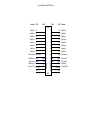
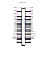
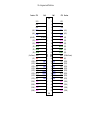
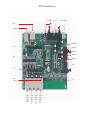
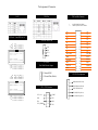
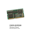
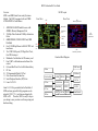
M502 Evaluation Kit User Guide
Overview
M502 is an ARM9-based Linux ready System on
Module. The M502 is equipped with an ATMEL
AT9SAM9G20 SoC and features:
1.
2.
3.
4.
5.
6.
7.
8.
9.
10.
11.
12.
13.
ARM926EJ-S ARM Thumb Processor with
400MHz, Memory Management Unit
32-KByte Data Cache and 32-KByte Instruction
Cache
64MB SDRAM, 128MB NAND Flash, 2MB
DataFlash
One 10/100 Mbps Ethernet with MAC/PHY and
transformer
Two USB 2.0 full speed (12 Mbps) Host Ports,
One USB client port
Multimedia Card Interface for SD memory card
Four UARTs with hardware and software flow
control
On board Real Time Clock with Lithium battery
I2C bus
32 Programmable Digital I/O Port
8-bit external local bus interface
Serial Peripheral Interface (SPI) Ports
Linux 2.6.29 OS
Linux 2.6.29 OS is pre-installed in the flash disk of
M502 and many powerful utility programs are also
included. GNU C/C++ tool chain are shipped with
M502 in CD.
Therefore, M502 is ready to drop in
your design to save your time in software porting and
hardware debug.
M-502 Layout
Front View
Rear View
RTC
CN3
2mm 2x25 pins header
Φ 2mm (M2)
Debug Port
JP4
CN1
2mm 2x
14 pins header
JTAG Port
CON1
JP2/JP3
Internal use
JP1
Internal
use
CN2
2mm 2x25 pins header
Function Block Diagram
USB Client x1
SD bus
USB Host x2
8-bit Local Bus
ARM9
SDRAM
Battery
I2S bus
NAND Flash
RTC/WD
Data Flash
32 GPIO
UART x4
I2C bus
SPI bus
PHY
LAN Coil
RS-232
32 GPIO
Serial Console
M502 Hardware Specifications
SoC: ATMEL AT91SAM9G20
CPU: ARM926EJ-S ARM Thumb Processor with Memory Management Unit (MMU)
Clock: 400MHz
SDRAM: 64MB
Flash: 128MB NAND Flash and 2MB Data Flash
Ethernet: 10/100 Mbps with MAC/PHY and Transformer
PHY: DAVCOM DM9161
Transformer: 1.5 KV isolation
Signal: ETX0+, ETX0-, ERX0+, ERXUSB Host: USB 2.0 full speed (12Mbps) Host x2
Signal: UDataA+, UDataA-, UDataB+, UDataBUSB Device: DDP (data+), DDM (data-), UDIO (I/O)
UART: Four Universal Asynchronous Receiver and Transmitter
Data Bits: 5 to 9 bits
Parity: None, Even, Odd, Mark, Space
Stop: 1, 1.5, 2 bits
Baud Rate: Up to 921.6 Kbps
Flow Control: RTS/CTS, XON/XOFF, None
RS485 Driver Control Signal (RTS0~RTS3)
Signal Level: CMOS/3.3V compatible
COM1: TXD0, RXD0, RTS0, CTS0
(Software configurable RS-232/485 mode)
COM2: TXD1, RXD1, RTS1, CTS1, DCD1, DTR1, DSR1
(Software configurable RS-232/485 mode)
COM3: TXD2, RXD2, RTS2, CTS2
(Software configurable RS-232/485 mode)
COM4: TXD3, RXD3, RTS3, CTS3
(Software configurable RS-232/485 mode)
Inter-IC Bus: (I2C Bus)
Compatible with standard two-wire serial memory interface
Supported Devices: (built-in)
Real Time Clock: ST M41T81 (option:Ricoh RS5C372A)
Watchdog Timer: ST M41T81
Backup battery: Lithium Battery (BR 1225 3V 48mAh)
GPIO controller: NXP PCA9539 (32 GPIO)
Signal: TWD, TWDK
I2S (internal IC Sound):
Transmitter: TSCK, TWS, TSD
Receiver: RSCK, RWS, RSD
Supported Device: Audio codec TI TLV320AIC23
Serial Peripheral Interface: (SPI)
Two chip Selects with external decoder
Three wires signals: MISO, MOSI and SPCK clock
Signal: MISO, MOSI, SPCK, CS1, CS2
Supported Device: ATMEL Dataflash
Multimedia Card Interface
Compatible with SD memory card Specification 1.0
Signal: MCCDA, MCCK, MCDA0, MCDA1, MCDA2, MCDA3
Programmable DIO ( I/O Controller NXP PCA9539)
32 General Purpose I/O can be programmable as digital input or output
Signal Level: CMOS/TTL Compatible
Input:
Low level: -0.5V min
+0.9V max
High level: +2.3V min
+5.5V max
Output:
Low level: +0.5V min @ 8mA
High level: +1.8V min @ 8mA
Signal: I/O_0 to I/O_31
Note: PIO24 to PIO31 are reserved for RS-232/422/485 interface selection for
serial ports 1 to 4. Please contact Artila if you want to use PIO24 to PIO31.
External Bus Interface:
8-bit data bus
Signal: D0~D7
8-bit address bus
Signal: A0~A7
3 Chip Selection
Signal: NCS0/NCS5/NCS6
Signal Level: CMOS/3.3V
Predefine Pins:
Reset Button (CN2, pin#35, RST#1), input
Buzzer (CN2, pin#37, BUZR), output
System ready LED (CN2, pin#38, RDY_LED), output
LAN activity LED (CN3, pin#11, ACT_LED), output
DIP_SW0, DIP_SW1, input
Debug Port: JP4
Serial Console: RS-232 TX/RX
Signal: DTXD_232, DRXD_232
JTAG: For low level debug
Signal: NTRST, TDI, TMS, TCK, TDO
Power:
Input: 3.0 to 3.6VDC (3.3V nominal)
Consumption: 2.5W
M502 Software Specifications
OS: Linux 2.6.29
Boot Loader: U-Boot 1.1.2
File System: JFFS2, EXT2/EXT3, VFAT/FAT, NFS
Protocol Stacks:
IPV4, ICMP, ARP, DHCP, NTP, TCP, UDP, FTP,
Telnet, HTTP, PPP, PPPoE, CHAP, PAP, SMTP, SNMP
V1/V3, SSL, SSH 1/2
Utilities:
Bash: Shell Command
Tinylogin: Login and user manager utility
Telnet: Telnet client program
Busybox: Linux utility collection
FTP: FTP client program
Daemon
pppd: Dial In/out over serial port and PPPoE
snmpd: SNMP agent program
telnetd: Telnet server program
inetd: TCP server program
ftpd: FTP server program
boa: Web server program
sshd: secured shell server
iptables: Firewall service manager
armd: Artila manager daemon
Tool Chain for Windows/Linux
GCC: C/C++ PC cross compiler
GLIBC: POSIX Library
Standard Device Drivers:
ttyS0: serial console port (AT91SAM9G20 debug port)
ttyS1~ttyS4: serial ports (AT91SAM9G20
UART0~UART3)
gpio: General Purpose I/O ( Controller NXP PCA9539)
mmc: SD/MMC:
rtc: Real Time Clock (ST m41t81)
sda: USB flash memory disk
ttyACM: USB Modem
ttyUSB: USB RS-232 adaptor
spi: spi bus
Default Setting
Default IP Address:192.168.2.127
Netmask: 255.255.255.0
ssh Login: root
Password: root
Telnet Login: guest
Password: guest
Terminal type: VT100
I/O Devices Control
M-502 uses standard I/O device control to access following devices:
1.
Ethernet: eth0
2.
Serial Ports: ttyS1, ttyS2, ttyS3,ttyS4
3.
Serial Console Port: ttyS0
4.
Real time clock: rtc0
5.
USB Flash Disk: sda, sda1, sdb, sdb1
6.
SD memory Card: mmc0
7.
USB WLAN dongle: wlan0
8.
USB Serial Cable: ttyUSB0, ttyUSB1
9.
SPI bus: spi0, spi1
Remark: Remember to include the “matrix504.h” header file in your
program. Please refer to the example program included in the M-502 SDK
CD to demo the RS-232/422/485 mode configuration of serial port 1
configuration.
File System
Matrix 504 uses ubi file system for the built-in flash memory
disk. The files system is stored at NAND flash memory.
Mount External Disk
To mount the USB Flash Disk and SD memory card, use
following commands after the disk are installed properly. To
mount USB disk
mount /mnt/sda or mount /mnt/sda1 or mount /mnt/sdb or
mount /mnt/sdb1
To find out the device name of the USB disk, you can use
dmesg | grep sd
And to mount SD memory card
mount /mnt/mmc
Web Page Directory
The web pages are placed at /usr/www and the /etc/lighttpd.conf
contains the lighttpd web server settings. The home page name
should be index.html
Welcome Message
The welcome message “Artila” can be modified by editing the /
etc/motd file.
Manager Utility Software
The Manager Utility software, manager.jar is a java program
and is used to discovered the Matrix 504 in the network if the IP
address is forgotten. It can be run at any OS where java run time
is available. To install the java run time platform at your
computer, please visit http://java.sun.com and download the
Java 2 Standard Edition (J2SE). Once the Matrix 500 is found,
you can click the Telnet Console to configure the Matrix 500
Note: Please refer to the software guide for the software
operation!!
Pin Assignment and Definition
Function
CPU
SoM
SoM
CPU
Function
CN1
(Addr Bus)
A0
1
2
D0
(Data Bus)
(Addr Bus)
A1
3
4
D1
(Data Bus)
(Addr Bus)
A2
5
6
D2
(Data Bus)
(Addr Bus)
A3
7
8
D3
(Data Bus)
(Addr Bus)
A4
9
10
D4
(Data Bus)
(Addr Bus)
A5
11
12
D5
(Data Bus)
(Addr Bus)
A6
13
14
D6
(Data Bus)
(Addr Bus)
A7
15
16
D7
(Data Bus)
(Write Enable)
NWE NWR0
17
18
NRD
(USB-Device-)
DDM
DDM 19
20 CS5
NCS5
(Chip Select)
NCS6
CS6 21
22 CS0
NCS0
(Chip Select)
(USB-Device+)
DDP
DDP 23
24
IRQ0
(Interrupt 0)
(Console TXD)
DTXD_232
25
26
DRXD-232
VCC3
27
28
GND
(Chip Select)
CN1
(Read Enable)
(Console RXD)
Pin Assignment and Definition
Function
CPU
SoM
SoM
CPU
Function
CN2
(COM2)
CTS2
1
2
DSR2
(COM2)
(COM2)
RTS2
3
4
RXD3
(COM3)
(COM3)
TXD3
5
6
CTS3
(COM3)
(COM3)
RTS3
7
8
TXD4
(COM4)
(COM4)
RXD4
9
10
RTS4
(COM4)
(COM4)
CTS4
11
12 DIP_SW
13
15
17
19
21
23
25
27
29
31
33
14
16
18
20
22
24
26
28
30
32
34
35
36
37
39
41
43
45
38
40 TSCK
42 RSD
44 RWS
46
GND
47
48
GND
VCC3
49
50
VCC3
(DIP_SW)
(GPIO)
(GPIO)
(GPIO)
(GPIO)
(GPIO)
(GPIO)
(USB B+)
(USB A-)
(GPIO)
(GPIO)
(Reset Btn)
(Buzzer)
(I2S transmitter)
(I2S transmitter)
(I2S receiver)
PB13
I/O_17
I/O_19
I/O_21
I/O_23
I/O_25
I/O_27
HDPB
HDMA
I/O_29
I/O_31
DIP_SW
PIO17
PIO19
PIO21
PIO23
PIO25
PIO27
UdataB+
UdataAPIO29
PIO31
BTNRST#
PA26
TF0
TD0
RK0
GND
BUZR
TWS
TSD
RSCK
CN2
PIO16
PIO18
PIO20
PIO22
PIO24
PIO26
PIO28
UdataBUdataA+
PIO30
PB12
I/O_16
PC1/PCK0
I/O_20
I/O_22
I/O_24
I/O_26
I/O_28
HDMB
HDPA
I/O_30
VCC3 PWROK
UDIO
PC6
TK2
RD2
RF2
GND
(DIP_SW)
(GPIO)
(GPIO)
(GPIO)
(GPIO)
(GPIO)
(GPIO)
(GPIO)
(USB B-)
(USB A+)
(GPIO)
(System Reset)
(USB-Device I/O)
(System Ready LED)
(I2S transmitter)
(I2S receiver)
(I2S receiver)
Pin Assignment and Definition
Function
CPU
SoM
SoM
CPU
Function
CN3
VCC3
1
2
VCC3
GND
3
4
GND
GND
5
6
GND
(LAN)
ERX0-
7
8
ERX0+
(LAN)
(LAN)
ETX0-
9
10
ETX0+
(LAN)
(LAN LED)
ACTLED# 11
12
MISO
(SPI)
(SPI)
MOSI
13
14
SPCK
(SPI)
(SPI)
NPCS0
15
16
NPCS3
(SPI)
(SD)
MCCK
17
18
MCCDA
(SD)
(SD)
MCDA0
19
20
MCDA1
(SD)
(SD)
MCDA2
21
22
MCDA3
(SD)
(Card Detect)
SDCD
23
24
SDWP
(SD Write Protect)
(I2C)
(GPIO)
(GPIO)
(GPIO)
(GPIO)
(GPIO)
(GPIO)
(GPIO)
(GPIO)
(COM1)
TWD
I/O_1
I/O_4
I/O_6
I/O_8
I/O_10
I/O_12
I/O_14
I/O_0
26
28
30
32
34
36
38
40
42
44
TWCK
I/O_3
I/O_5
I/O_7
I/O_9
I/O_11
I/O_13
PC15
I/O_2
TXD1
25
27
29
31
33
35
37
39
41
43
RXD1
(I2C)
(GPIO)
(GPIO)
(GPIO)
(GPIO)
(GPIO)
(GPIO)
(GPIO)
(GPIO)
(COM1)
(COM1)
CTS1
45
46
RTS1
(COM1)
(COM2)
DTR2
47
48
TXD2
(COM2)
(COM2)
RXD2
49
50
DCD2
(COM2)
PIO1
PIO4
PIO6
PIO8
PIO10
PIO12
PIO14
PIO0
CN3
PIO3
PIO5
PIO7
PIO9
PIO11
PIO13
PIO15
PIO2
M501 Evaluation Board Layout
Reset Button
GPIO 0~15
Power +9~40VDC
LAN 1
USB 2.0 Host
DIP Switches
CN2
Power LED
Ready LED
LAN Link/Act
CN1
GPIO 16~31
CN8
CN3
LED
COM1 ~4
CN7
COM1
RS-232
RS-422
RS-485
COM2
RS-232
With
RTS
CTS
COM3
RS-232
With
RTS
CTS
COM4
RS-232
With
RTS
CTS
Pin Assignment of Connectors
LAN 1
COM Port
CN8 Local Bus Connector
1.
2.
A0
A1
A2
GPIO Port 0~15 and GPIO Port 16~31
DIO2
A6
RxD
A7
VCC3
NWE_NWR0
GND
DDM
PC13/NCS6
DIO1
JP1 of M502
Boot Mode Selection Jumper
DIO16
1
2
3
DDP
DTXD_232
VCC3
2-3: Internal ROM
1-2: External Flash (Default)
1
DIO4
DIO0
1
3
TxD
4
2
DIO3
DIO18
DIO17
DIO6
DIO8
1
2
3
4
1
2
3
4
5
6
7
8
9
10
11
12
13
14
15
16
17
18
19
20
21
22
23
24
25
26
27
28
CN7 (SPI) Pin Assignment
1
MISO (Master In Slave Out)
2
MOSI (Master Out Slave In)
3
SPCK (SPI Serial Clock)
4
NPCS0 (SPI Chip Select 0)
5
NPCS3 (SPI Chip Select 3)
4
2
DIO19
6
DIO22
DIO20
5
3
5
6
7
10
8
DIO9
DIO7
DIO5
DIO24
DIO26
A4
A5
CON1 JTAG Connector
DIO25
DIO23
DIO21
10
8
7
DIO10
DIO12
13
11
9
12
14
DIO13
DIO11
DIO28
13
11
9
12
14
DIO29
DIO27
GND
DIO14
15
16
DIO15
15
16
DIO31
19
17
18
20
+3.3V
GND
GND
DIO30
+5V
19
17
18
20
+3.3V
GND
+5V
JP4 Serial Console Port
A3
1x14 Pin Header Pitch 2.54mm
CN8 directly connect to CN1 of M501
VCC3 (3.3V)
1
2
NTRST
GND
3
4
TDI
TDO
5
6
TMS
VCC3_PWROK
7
8
TCK
D0
D1
D2
D3
D4
D5
D6
D7
NOE_NRD
NCS5
NCS0
IRQ0
DRXD_232
GND