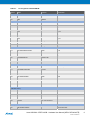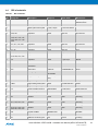
1
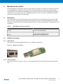
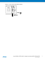
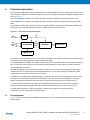
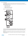
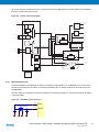
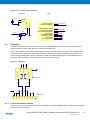
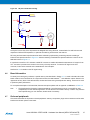
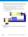
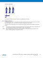
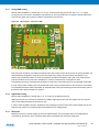
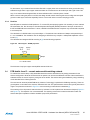
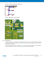
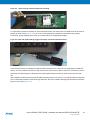
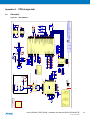
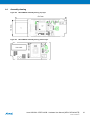
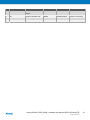
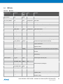
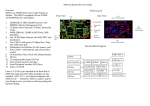
APPLICATION NOTE
Atmel AVR2030: ATRF231USB – Hardware User Manual
8-bit Atmel Microcontrollers
Features
•
High-performance, low-power Atmel® 32-bit ARM® CORTEX™-M3 RISC
microcontroller ATSAM3S4BA
• 256kB High-Speed Flash
• 48kB SRAM
• Wide variety of peripheral components
•
•
•
•
•
•
Onboard 2GB flash memory to store user defined data
Onboard 2.4GHz radio transceiver AT86RF231 and ceramic chip antenna
Powered over USB connector type A soldered on PCB
Three free programmable status LEDs
RF shielding
Interfaces: DBGU, JTAG, USB
Introduction
This manual describes the RF231USB Reference Design which is equipped with a
powerful CORTEX-M3 microcontroller in combination with the Atmel 2.4GHz
AT86RF231 radio transceiver and an onboard ceramic chip antenna.
Detailed information is given in the individual sections about the radio stick
functionality, the available interfaces, and the stick design.
The USB radio stick comes pre-flashed with a boot loader and a corresponding tool
for uploading of application firmware; it is stored on the onboard external 2GB flash
memory. The stick can be operated as full functional wireless node via the USB port
allowing direct communication with the host PC. It provides the way to demonstrate
wireless software applications and allows adding RF-functionality to other hardware.
Figure 1.
Top and bottom view of RF231USB-RD stick.
42018A−AVR−08/2012
Table of Contents
1. Disclaimer ............................................................................................ 4 2. Overview .............................................................................................. 4 3. Mechanical description ........................................................................ 6 3.1 Dimensions ....................................................................................................... 6 3.2 Interface connectors.......................................................................................... 6 3.2.1 USB interface ...................................................................................... 6 3.2.2 10-pin connector ................................................................................. 6 4. Functional description .......................................................................... 8 4.1 Pin assignment.................................................................................................. 8 4.2 Power supply................................................................................................... 10 4.3 Microcontroller................................................................................................. 10 4.3.1 Clock generator ................................................................................ 11 4.3.2 Microcontroller clock ......................................................................... 12 4.4 On-board radio transceiver ............................................................................. 13 4.4.1 Radio transceiver reference clock (CLKM) ....................................... 13 4.5 RF section ....................................................................................................... 14 4.5.1 Cermic chip antenna connection ....................................................... 14 4.6 Board information ............................................................................................ 15 4.7 On-board peripherals ...................................................................................... 15 4.7.1 Flash ………….. ................................................................................ 16 4.7.2 USB type A plug ............................................................................... 16 4.7.3 10-pin connector ............................................................................... 17 4.7.4 Status LEDs ...................................................................................... 17 4.7.5 ERASE and VCC pins....................................................................... 18 5. PCB layout description ....................................................................... 19 5.1 PCB detail 1 – balanced RF pin fan out .......................................................... 20 5.2 PCB detail 2 – crystal routing .......................................................................... 21 5.3 PCB detail 3 – ground plane routing and feed line design .............................. 21 5.3.1 Analog GND routing .......................................................................... 22 5.3.2 Digital GND routing ........................................................................... 22 5.3.3 GND plane ........................................................................................ 22 5.3.4 Feed line ........................................................................................... 23 5.4 PCB details 4 and 5 – ceramic antenna with matching network ...................... 23 5.4.1 Antenna tuning .................................................................................. 24 5.4.2 Range measurement ........................................................................ 26 5.5 PCB detail 6 – coaxial connector .................................................................... 27 6. Programming ..................................................................................... 28 6.1 JTAG interface ................................................................................................ 28 6.2 USB interface ROM bootloader ....................................................................... 28 7. Electrical characteristics .................................................................... 29 7.1 Absolute maximum ratings .............................................................................. 29 7.2 Recommended operating range ...................................................................... 29 7.3 Current consumption ....................................................................................... 29 7.4 RF characteristics ........................................................................................... 29 8. Abbreviations ..................................................................................... 31 Appendix A. PCB design data ........................................................... 32 A.1 Schematic ....................................................................................................... 32 Atmel AVR2030: ATRF231USB – Hardware User Manual [APPLICATION NOTE]
42018A−AVR−08/2012
2
A.2 A.3 A.4 Assembly drawing ........................................................................................... 33 Bill of materials ................................................................................................ 34 MIB data .......................................................................................................... 36 Appendix B. Radio certification .......................................................... 38 B.1 United States (FCC) ........................................................................................ 38 B.2 Europe (ETSI) ................................................................................................. 39 Appendix C. References .................................................................... 40 Appendix D. Revision history RF231USB PCBA ............................... 41 Appendix E. EVALUATION BOARD/KIT IMPORTANT NOTICE....... 42 Atmel AVR2030: ATRF231USB – Hardware User Manual [APPLICATION NOTE]
42018A−AVR−08/2012
3
1.
Disclaimer
Typical values contained in this application note are based on simulations and testing of individual examples.
Any information about third-party materials or parts was included in this document for convenience. The vendor may
have changed the information that has been published. Check the individual vendor information for the latest changes.
2.
Overview
The compact designed RF231USB radio sticks are based on the efficient CORTEX-M3 microcontroller architecture with
256kB High-Speed flash and 48kB SRAM [1]. Additional 2GB flash memory to store user defined data is provided with
the RF231USB-RD; it is usable as mass storage device.
Operating at the transmission frequency of 2.4GHz, the ATMEL low-power transceiver AT86RF231 [2] is integrated. It
provides a complete radio transceiver interface between the antenna and the microcontroller and an extended
functional range such as a 128-Bit AES hardware engine to assure data security.
Figure 2-1. Main components (RF shield removed).
USB plug
Microcontroller (MCU)
MCU clock XTAL
ERASE / VCC
pins
Status
LEDs
ceramic antenna
Transceiver and clock XTAL
2GByte
Flash
10 pin
connector
Voltage
regulator
Top side
Bottom side
The USB radio stick provides programming and debugging interfaces to the user.
Comprehensive user documentation, device drivers as well as a bootloader application (which is running on the host
PC) are stored to the mass storage device.
The serial bootloader functionality allows uploading of application firmware through the USB connection, without the
need for extra programming tools. This functionality is provided by the bootloader firmware pre-flashed to the
RF231USB board in delivery condition.
Atmel AVR2030: ATRF231USB – Hardware User Manual [APPLICATION NOTE]
42018A−AVR−08/2012
4
A JTAG interface targets software development. Here an Atmel SAM-ICE™ adapter with a suitable programmer has to
be connected to the USB stick. The boards have to be assembled as shown in Figure 2-2. The RF231USB-RD board is
attached with its JTAG connector to the SAM-ICE adapter. The SAM-ICE JTAG emulator which is used to program a
new image into the ARM MCU on RF231USB-RD board is connected to the SAM-ICE adapter and to the PC.
Figure 2-2. USB radio stick (left-hand) with the SAM-ICE programmer.
The RF231USB-RD USB radio stick provides the way to demonstrate software applications like:
•
•
•
Wireless UART in ASF
Wireless network sniffer, for example hardware for third party solutions like Luxoft and Perytons
Complex wireless network solutions, for example ZigBee® Home Automation
The RF231USB-RD stick allows adding RF-functionality to other hardware or kit deliveries:
•
Wireless gateway for PC hardware, for example Reference design for wireless passive infrared camera Atmel
kit ATSAM4S-WPIR-RD
•
Point to point connection between PCs (wireless UART)
Atmel AVR2030: ATRF231USB – Hardware User Manual [APPLICATION NOTE]
42018A−AVR−08/2012
5
3.
Mechanical description
The RF231USB-RD is manufactured using a four-layer printed circuit board. The components mounted on the top side
are: ATSAM3S4BA microcontroller and low-power radio transceiver AT86RF231 (including their crystal oscillators),
2.45GHz antenna and the SMD-mounted USB type A plug. The bottom side of the board is equipped with the following
components and connectors (among other): 2GB additional flash chip, 10-pin connector, three status LEDs, ERASE
and VCC pins, voltage regulator for power supply.
3.1
Dimensions
Due to size constraints, components are placed on the top side as well as on the bottom side of the board. The USB
plug is mounted on edge of the board. Board width and height were chosen so that multiple USB sticks will fit beside
each other in standard USB hubs. Board length is determined by size of the ground plane which is approximately λ\2 for
2.4GHz band.
Table 3-1.
RF231USB-RD mechanical dimensions.
Dimension
Value
Length x
63.5mm (including USB plug)
Width y
19.0mm
Height z
5.5mm (without JTAG/debug header)
9.5mm (with JTAG/debug header)
3.2
Interface connectors
3.2.1
USB interface
The connector for the RF231USB-RD radio stick, X1, is USB type A chassis plug.
Figure 3-1. USB type A connection.
3.2.2
10-pin connector
The 10-pin connector, X2, with its 2 x 5 pins of 1.27mm (50mil) pitch is directly accessible from the USB stick bottom
side.
Atmel AVR2030: ATRF231USB – Hardware User Manual [APPLICATION NOTE]
42018A−AVR−08/2012
6
Figure 3-2. 10-pin connector with footprint receptacle.
Atmel AVR2030: ATRF231USB – Hardware User Manual [APPLICATION NOTE]
42018A−AVR−08/2012
7
4.
Functional description
The Atmel RF231USB-RD stick carries a high-performance Atmel CORTEX-M3 microcontroller, which connects to the
radio transceiver AT86RF231 and various peripheral units. The block diagram of the RF231USB-RD USB radio stick is
shown in Figure 4-1.
The Atmel AT86RF231 interfaces the ceramic chip antenna which is designed at the outermost location of the
RF231USB-RD stick to provide sufficient signal strength and quality to reach line of sight distances of greater than
200m.
The transceiver is interfaced by the MCU via SPI and several GPIO lines. Two separate IRQ lines are available and
routed to MCU pins optionally acting as timer inputs. CLKM outputs the transceiver clock.
Figure 4-1. Functional overview block diagram.
VUSB
4.5 .. 5.5V
JTAG
DBGU
USB
VCC
VCC
3.3V
SPI
ATSAM3S4BA
GPIO
AT86RF231
Chip antenna
IRQ
MMC
2 GByte Flash
The critical RF components mounted on the board are encapsulated. A RF shielding is affixed at the board top side to
house these components to guarantee an EMI shielded environment.
The ATSAM3S4BA has a flexible clock system. Primarily the onboard 18.432MHz crystal clocks a phase-locked loop
(PLL) from which the microcontroller core and all of its internal peripheral units are sourced. The radio transceiver
provides additional clock inputs.
The soldered USB type A plug represents an USB 2.0 interface and can be used as programming and debugging
interface by default. It is used to power the RF231USB-RD stick. The 3.3V supply voltage is generated by a LDO
voltage regulator mounted at the bottom side of the board.
The USB stick is populated with a 2GB flash memory on its bottom side to store user defined data. The flash is also
intended to be used as mass storage device. Board-specific information such as board identifier, the node MAC
address, and production calibration values are stored in a special upper memory block of the flash memory.
A 10-pin connector assembled at the bottom side is designed for programming via JTAG interface. A matching
programming adapter that is equipped with a 20-pin standard ARM-JTAG connector has to be used for this.
To deliver status information, a basic user interface consisting of three LEDs is provided on the board.
An ERASE pin can be used to delete the flash’s content.
4.1
Pin assignment
In Table 4-1 an overview of the RF231USB-RD’s pin assignment of components and peripherals together with operating
options is given.
Atmel AVR2030: ATRF231USB – Hardware User Manual [APPLICATION NOTE]
42018A−AVR−08/2012
8
Table 4-1.
µC Pin
Pin assignment of RF231USB-RD.
Name
Function
Comments
USB connector X1
56
DDM
USB DM
57
DDP
USB DP
10-pin connector X2
53
PB7/TCK/SWCLK
JTAG TCK
GND
49
pin 1
pin 2
PB5/TWCK1/PWML0/WKUP13/TDO
JTAG TDO
VCC
pin 3
pin 4
51
PB6/TMS/SWDIO
JTAG TMS
pin 5
39
NRST
/Reset
pin 6
VCC
pin 7
30
PA9/URXD0/NPCS1/PWMFI0
Debug RXD
pin 8
33
PB4/TWD1/PWMH2/TDI
JTAG TDI
pin 9
29
PA10/UTXD0/NPCS2
Debug TXD
pin 10
Miscellaneous
13
PA19/RK/PWML0/A15/AD2
LED1
red
9
PA17/TD/PCK1/PWMH3/AD0
LED2
yellow
10
PA18/RD/PCK2/A14/AD1
LED3
green
35
PA5/RXD0/NPCS3
Hardware ID1
34
PA6/TXD0/PCK0
Hardware ID2
32
PA7/RTS0/PWMH3/XIN32
Hardware ID3
Internal transceiver interface
20
PA15/TF/TIOA1/PWML3
RXTS/DIG2
Timestamp
11
PA21/RXD1/PCK1/AD8
SLP-TR
21
PA14/SPCK/PWMH3
SCK
SPI
27
PA12/MISO/PWMH1
MISO
SPI
22
PA13/MOSI/PWMH2
MOSI
SPI
28
PA11/NPCS0/PWMH0
SELN
47
PA1/PWMH1/TIOB0/A18
IRQ
23
PA24/RTS1/PWMH1/A20
RST
36
PA4/TWCK0/TCLK0
CLKM
Transceiver Reset
2GB flash memory
42
MCDA0
ext. Flash Data 0
52
MCDA1
ext. Flash Data 1
26
MCDA2
ext. Flash Data 2
37
MCDA3
ext. Flash Data 3
38
MCCDA
ext. Flash Command
41
MCCK
ext. Flash Clock
Erase pin
55
PB12/PWML1/ERASE
Erase MCU flash
Atmel AVR2030: ATRF231USB – Hardware User Manual [APPLICATION NOTE]
42018A−AVR−08/2012
9
For a description of component signals see Table 4-2:
Table 4-2.
Signal description list.
Signal name
Function
Type
DDM
USB Full Speed Data –
DDP
USB Full Speed Data +
Analog
Digital
Active level
Comments
Power – USB connector
JTAG
TCK
Test Clock
Input
onboard Pull-up
TDI
Test Data In
Input
onboard Pull-up
TDO
Test Data Out
Output
TDM
Test Mode Select
Input
Microcontroller Reset
I/O
URXD0
UART Receive Data
Input
UTXD0
UART Transmit Data
Output
onboard Pull-up
Reset
RSTN
Low
Pull-Up resistor
UART0
4.2
Power supply
Both ATSAM3S4BA microcontroller and AT86RF231 radio transceiver are powered over the USB connector type A,
soldered on the PCB. The available 5V (VUSB) voltage is transformed to the required 3.3V by the voltage regulator
LDO 3.3V (IC1) which is integrated into the power supply line and mounted at the bottom side of the board.
Figure 4-2. Voltage regulator.
IC1
8
VUSB
6
IN
OUT
EN
BYP
1
4
C2
FB
1µF
2
7
n.c.
n.c.
GND
GND
VCC
C8
C4
100nF
1µF
3
5
0
TPS79433DGN
GND
4.3
GND
GND
Microcontroller
The Atmel SAM3S is a family of flash microcontrollers based on the high performance 32-bit ARM Cortex-M3 RISC
processor. It operates at a maximum speed of 64MHz and features 256Kbytes of flash and 48Kbytes of SRAM.
The ATSAM3S4BA device [1] is a medium range general purpose microcontroller with the best ratio in terms of reduced
power consumption, processing power and peripheral set. This enables the ATSAM3S4BA to sustain a wide range of
applications including consumer, industrial control, and PC peripherals.
Atmel AVR2030: ATRF231USB – Hardware User Manual [APPLICATION NOTE]
42018A−AVR−08/2012
10
4.3.1
Clock generator
The ATSAM3S4BA has a flexible clock system, supporting a large number of clock sources. It incorporates both
calibrated integrated and external crystal oscillators and resonators. The Atmel SAM3S family allows dynamic switching
between the following clock sources:
•
•
•
•
Embedded 32kHz RC oscillator
32.768kHz crystal oscillator
Embedded 4/8/12MHz fast RC oscillator
3-20MHz crystal or ceramic oscillator
Figure 4-3. Clock generator block diagram.
C lo c k G e n e r a t o r
X TA L S E L
( S u p p ly C o n t r o l l e r )
Em bedded
32 kH z
R C O s c i ll a t o r
S lo w C lo c k
SLCK
X IN 3 2 /PA 7
32768 H z
C r y s ta l
X O U T 3 2 /PA 8
O s c illa to r
M OSCSEL
Em bedded
4 /8 / 1 2 M H z
Fast
1
0
R C O s c illa to r
M a in C lo c k
M A IN C K
3 -2 0 M H z
X IN /P B 9
C r y s ta l
or
C e r a m ic
X O U T /P B 8
R e s o n a to r
O s c illa to r
PLLA and
P L L A C lo c k
D iv id e r / 2
PLLAC K
P L L A D IV 2
PLLB and
D iv i d e r / 2
P L L B C lo c
PLLBC K
P L L B D IV 2
S ta tu s
C o n tro l
Pow er
M anagem ent
C o n t r o l le r
From these, four different internal clocks are generated: Both 32kHz oscillators may trigger the slow clock, suitable for
low power modes. The two remaining sources are inputs to the Main clock as well as to two high frequency phaselocked loop (PLL) clocks, whereas variable multipliers and dividers can be applied to generate a wide range of clock
frequencies.
After reset, the device will always start up running from slow clock. Usually the other clock sources are set up and
switched to during initialization. In normal operation, the system clock source and prescalers can be changed from
software at any time.
Atmel AVR2030: ATRF231USB – Hardware User Manual [APPLICATION NOTE]
42018A−AVR−08/2012
11
All clock sources are controlled and may be monitored by the Power Management Controller (PMC) which distributes
the clock to all internal functional units.
Figure 4-4. General clock block diagram.
C lo c k G e n e ra to r
P ro c e s s o r
X TA L S E L
P r o c e s s o r c lo c k
C lo c k
HCLK
C o n t r o lle r
( S u p p ly C o n t r o ll e r )
in t
S le e p M o d e
Em bedded
32 kH z R C
O s c ill a t o r
D iv i d e r
S l o w C lo c k
S y s T ic k
/8
SLCK
M a s t e r C l o c k C o n t r o l le r
X IN 3 2 /PA 7
32768 H z
SLCK
F r e e r u n n i n g c lo c k
(P M C _ M C K R )
C r y s ta l
FCLK
O s c ill a t o r
X O U T 3 2 /PA 8
M A IN C K
PLLBC K
MOSCSEL
PRES
PLLAC K
MCK
/1 6 ,/3 2 ,/6 4
4 /8 /1 2 M H z
P e r ip h e r a ls
1
0
Fast
M a s t e r c lo c k
P re s c a le r
/1 ,/2 ,/3 ,/4 ,/8 ,
Em bedded
C lo c k C o n t r o lle r
R C O s c illa t o r
(P M C _ P C E R x )
O N /O F F
M a in C l o c k
p e r ip h _ c lk [ . .
M A IN C K
3 -2 0 M H z
C r y s ta l
X IN /P B 9
or
C e r a m ic
P r o g r a m m a b le C l o c k C o n t r o l le r
R e s o n a to r
X O U T /P B 8
O s c ill a t o r
(P M C _ P C K x )
SLC K
M A IN C K
PLLB C K
PLLA and
D iv id e r / 2
P L L A C lo c k
PLLAC K
PRES
P r e s c a le r
O N /O F F
/1 ,/2 ,/4 ,/8 ,
p c k [..]
/1 6 ,/3 2 ,/6 4
PLLAC K
P L L A D IV 2
U S B C l o c k C o n t r o lle r ( P M C _ U S B )
P LLAC K
P L L B C lo c k
PLLB and
D iv id e r / 2
PLLBC K
PLLBC K
U S B C lo c k
D iv i d e r
UDPCK
/1 ,/2 ,/3 ,...,/1 6
U S B D IV
P L L B D IV 2
S ta tu s
C o n tro l
Pow er
M anagem ent
C o n t r o ll e r
Microcontroller clock
The RF231USB-RD is populated with an external 18.432MHz crystal oscillator, Q1, assembled on the top side of the
printed circuit board close to the MCU. Connected to XIN/XOUT (pins 61 and 62) it delivers an accurate clock for the
ATSAM3S4BA.
Since the design is a USB device, low power modes are not expected (“always on”). Therefore no external 32.768kHz
crystal is provided.
Figure 4-5. 18.432MHz crystal connection.
62
22pF
GND
4
Q1
18.432MHz / CL=16pF
1
3
C17
C18
2
4.3.2
GND GND
61
PB9/XIN
PB8/XOUT
22pF
GND
Atmel AVR2030: ATRF231USB – Hardware User Manual [APPLICATION NOTE]
42018A−AVR−08/2012
12
4.4
On-board radio transceiver
With the AT86RF231, the board is equipped with a low-power 2.4GHz transceiver designed for industrial and consumer
IEEE® 802.15.4, ZigBee, RF4CE, SP100 and high data rate ISM applications. It is tuned with the onboard 2.45GHz
ceramic chip antenna. Interconnected with the MCU, it provides a compact radio interface on a single chip.
The transceiver comprises the analog radio transceiver and the digital modulation and demodulation including time and
frequency synchronization and data buffering. The number of external components is minimized such that only the
antenna, the crystal and decoupling capacitors are required. The bidirectional differential antenna pins are used for
transmission and reception, thus no external antenna switch is needed.
An internal 128byte RAM for RX and TX buffers the data to be transmitted or the received data. Two on chip low
dropout voltage regulators provide the internal analog and digital 1.8V supply.
The transceivers further contain comprehensive hardware-MAC support (Extended Operating Mode) and a security
engine (AES) to improve the overall system power efficiency and timing.
4.4.1
Radio transceiver reference clock (CLKM)
The integrated radio transceiver is clocked by a 16MHz reference crystal. The 2.4GHz modulated signal is derived from
this clock. Operating the node according to IEEE 802.15.4 [3], the reference frequency must not exceed a deviation of
±40ppm. The absolute frequency is mainly determined by the external load capacitance of the crystal, which depends
on the crystal type and is given in its datasheet.
The radio transceiver reference crystal, Q2, shall be isolated from fast switching digital signals and surrounded by a
grounded guard trace to minimize disturbances of the oscillation. Detailed layout considerations can be found in
Chapter 5.
The RF231USB-RD uses a SIWARD SMD/SX-4025 crystal with two load capacitors of 12pF each. To compensate for
fabrication and environment variations, the frequency can be further tuned using the radio transceiver register
XOSC_CTRL (0x12) (refer to [2], Appendix C).
The reference frequency is also available at the CLKM pin of the radio transceiver and depending on the related register
setting. It is divided by an internal prescaler, thus clock frequencies of 16MHz, 8MHz, 4MHz, 2MHz, 1MHz, 250kHz or
62.5kHz are possible. Initially the transceiver master clock is outputted prescaled by 16 (1MHz clock output; refer to [2]
for details).
CLKM is routed to the MCU (pin 36 / TWCK0) where it may be used as timer input. The signal is filtered by a low-pass
filter to reduce harmonic emissions within the 2.4GHz ISM band. The filter is designed to provide a stable 1MHz clock
signal with correct logic level to a microcontroller pin with sufficiently suppressed harmonics. CLKM frequencies above
1MHz would require a redesign of R11 and C28 which in the current device are covered by the RF shield. In case of RC
cut-off frequency adjustments, depending on the specific load and signal routing conditions, one may observe
performance degradation of channel 26. Since its possible influence on the radio performance it is recommended to
disable CLKM output if not needed.
Atmel AVR2030: ATRF231USB – Hardware User Manual [APPLICATION NOTE]
42018A−AVR−08/2012
13
Figure 4-6. Transceiver clock connection.
Transceiver
EVDD
15
MCU
DEVDD
C19
17
GND
PB13/PWML2/PCK0/DAC0
PB14/NPCS1/PWMH3/DAC1
DVSS
CLKM
DVSS
1µF
PA0/PWMH0/TIOA0/A17/WKUP0
PA1/PWMH1/TIOB0/A18/WKUP1
PA2/PWMH2/SCK0/DATRG/WKUP2
PA3/TWD0/NPCS3
PA4/TWCK0/TCLK0/WKUP3
PA5/RXD0/NPCS3/WKUP4
PA6/TXD0/PCK0
PA7/RTS0/PWMH3/XIN32
18
16
R11
CLKM
C28
470R
GND
1.5pF
GND
4.5
59
63
48
47
44
43
36
35
34
32
PLL_SAM7S
IRQ_SAM3S
CLKM
HWID1
HWID2
HWID3
RF section
The Atmel AT86RF231 radio transceiver incorporates all RF and BB critical components necessary to transmit and
receive signals according to IEEE 802.15.4 or proprietary ISM data rates.
A balun, B1, performs the differential to single-ended conversion of the RF signal to connect the Atmel AT86RF231 to
the ceramic antenna, passing a tuning line with a network of inductors and capacitors along the line. The balun unit’s
output connections (RFN, RFP / pins 3, 4) are directly routed to the differential RF I/O pins of the AT86RF231 radio
transceiver. Refer to Chapter 5 for further information about the antenna tuning.
Figure 4-7. 50Ω balun.
Balanced P2
unbalanced
GND
1
2
DC_GND
GND
4
B1
2450FB15L0001E
1
IC3
AT86RF231-ZU
DIG3
DIG4
AVSS
2
GND
3
4 RFP
RFP
RFN
5 RFN
RFP
RFN
6
AVSS
7
DVSS
RSTN
8
GND
4.5.1
6
nc
3
Balanced P1
5
p
Cermic chip antenna connection
The ceramic chip antenna is designed at the outermost location of the RF231USB-RD stick to enable good transmission
properties into the environment.
Atmel AVR2030: ATRF231USB – Hardware User Manual [APPLICATION NOTE]
42018A−AVR−08/2012
14
Figure 4-8. RF parts outside RF shielding.
ANT1
2450AT43B100
50Ohm i
C41
n.b.
GND
L2
1.5nH
L3
50Ohm i
X3
UFL
GND
2.2nH
C40
C33
22pF
22pF
50Ohm i
50Ohm
i
R2
10k
GND
GND GND
The layout in the vicinity of the chip antenna is designed as a tuning structure, a transmission line with inductors and
capacitors of defined load impedance, to optimize the matching of transceiver and antenna.
RF tuning and best antenna performance has been achieved by implementing a matching network consisting of
inductors and capacitors shown in Figure 4-8. Antenna matching is realized with capacitors effective in the line to the
50Ω balun shown in Figure 4-7.
It is optional to retrofit an U.FL miniature coaxial RF connector to enable cable based measurements. A footprint for an
U.FL connector is provided on the board in the vicinity of the chip antenna. To route the RF signal to the U.FL
connector, C40 must be removed and re-assembled on C33’s footprint.
See Section 4.5 for details on the RF signal routing.
4.6
Board information
To identify the board type by software, a special memory area described in Section 4.7.1 is used. Information about the
board contains, but is not limited to, its unique serial number, the MAC address (1), and calibration values. Stored in the
uppermost memory block of the external flash, the data are written during board production testing. These can be used
to optimize system performance.
For a complete description of all board data, features and options please refer to Appendix A, MIB data A.4 Table 8-2.
Note:
4.7
1.
The board-specific information is stored persistently in this flash memory block. It must NOT be used
competitively from the mass storage device. This is assured in the board’s delivery condition. Pay attention
when implementing your own firmware; double-check if necessary.
On-board peripherals
This section describes the important on-board peripherals: memory components, plugs and connectors as well as other
interface and access options to the board.
Atmel AVR2030: ATRF231USB – Hardware User Manual [APPLICATION NOTE]
42018A−AVR−08/2012
15
4.7.1
Flash
The Atmel RF231USB-RD is populated with a 2GB flash device (SDIN5D2-2G) for persistent data storage. The flash is
equipped with a memory controller and has an iNAND flash architecture. It complies with e.MMC Specification Version
4.4 such that it performs like a Multimedia Card (MMC) from the MCU view. Possible data bit modes are 1bit (default)
and 4bit.
It is typically applied as mass storage device for user defined data (if it is attached to a USB port of a PC).
In the upper memory block, board-specific information such as board identifier, the node MAC address
production calibration values are stored as described in Section 4.6.
(1)
, and
In custom implementations it may serve for storing complete firmware images of the Atmel ATSAM3S4BA.
1.
Note:
MAC addresses used for this package are Atmel property. The use of these MAC addresses for
development purposes is permitted.
Figure 4-9. MCU-flash interconnection.
GND
7
GND
GND
GND
C29
C30
C31
C32
C35
C36
1µF
1nF
100nF
100nF
100nF
100nF
GND
GND
GND
GND
GND
VDDCORE
VDDCORE
VDDCORE
12
24
60
46
17
2
GND
GND
GND
GND
GND
GND
VCC
Flash
IC4
SDIN2C2
J10
K9
E6
F5
FCAP
CLK
CMD
VDD_H
VDD_H
VDD_H
VDD_H
VDD_H
DAT3
DAT2
DAT1
DAT0
C2
/RST
MCDA2
MCDA3
MCCDA
MCCK
MCDA0
MCDA1
C5
2.2µF
M6
MCCK
M5
MCCDA
B2
A5
A4
A3
MCDA3
MCDA2
MCDA1
MCDA0
R20
100k
R21
100k
R22
100k
R23
100k
GND
C4
E7
G5
K8
N2
P6
P4
N5
VSS
VSS
VSS
VSS
VSS
VSS
VSS
VSS
P3
P5
M4
C6
N4
VDD_F
VDD_F
VDD_F
VDD_F
23
25
26
37
38
41
42
52
ATSAM3S4BA-AU
R24
10k
VCC
PA24/RTS1/PWMH1/A20/PIODC0
PA25/CTS1/PWMH2/A23/PIODC1
PA26/DCD1/TIOA2/MCDA2/PIODC2
PA27/DTR1/TIOB2/MCDA3/PIODC3
PA28/DSR1/TCLK1/MCCDA/PIODC4
PA29/RI1/TCLK2/MCCK/PIODC5
PA30/PWML2/NPCS2/MCDA0/WKUP11/PIODC6
PA31/NPCS1/PCK2/MCDA1/PIODC7
dresdenelektronik ingenie
GND
4.7.2
D-01237 Dresden Enno-Heide
USB type A plug
The USB type A chassis plug, X1, represents an USB 2.0 full-speed interface and can be used as programming and
debugging interface by default, for example to upload new firmware. It supplies the 5.0V operating voltage to run the
RF231USB-RD stick.
Atmel AVR2030: ATRF231USB – Hardware User Manual [APPLICATION NOTE]
42018A−AVR−08/2012
16
Figure 4-10. USB type A plug.
X1
VBUS
DD+
GND
SHLD1
SHLD2
1
2
3
4
S1
S2
VUSB
#USBDM
#USBDP
GND
SHLD
USB type A plug
A suppressor array, D1, is switched to the two USB data lines to safeguard data exchange.
Figure 4-11. Suppressor array.
VUSB
VUSB
#USBDM
#USBDP
4
5
6
GND
VCC
4.7.3
3
2
1
SHLD
GND
10-pin connector
The 10-pin connector, X2, is placed at the bottom side of the RF231USB-RD stick, near the USB type A plug (on the top
side).
Figure 4-12. 10-pin connector.
X2
TCK
TDO
TMS
VCC
TDI
1
3
5
7
9
2
4
6
8
10
GND
/RESET
DRXD
DTXD
VCC
Pin header 10P, 2-row
The soldered combined JTAG/Trace connector of the board enables programming, debugging and testing right in the
circuit. For programming via JTAG the 10-pin connector has to be plugged into the SAM-ICE female adapter.
4.7.4
Status LEDs
For simple applications and debugging purposes, or just to deliver status information, a basic user interface consisting
of three LEDs is provided directly on the board. They are mounted on the bottom side of the printed circuit board.
Atmel AVR2030: ATRF231USB – Hardware User Manual [APPLICATION NOTE]
42018A−AVR−08/2012
17
Figure 4-13. Status LEDs.
VCC
LED3
R15
470R
LGL29KG2J1-24-Z
R14
470R
LED2
LED1
TLMS1000-GS08
R13
470R
VCC
LYL29KJ1K2-26-Z
VCC
The LEDs are connected to the pins 9, 10 and 13 of the SAM3S4B microcontroller.
4.7.5
ERASE and VCC pins
The ERASE pin (see Section 4.1 Pin assignment) is used to reinitialize the MCU flash content - and some of its NVM
(Non-Volatile Memory) bits - to an erased state. The flash is transferred to its original state.
To perform a flash erase operation the pin has to be tied high longer than 220ms while the USB stick is connected to
the PC.
Note:
By electrically connecting the two test points ERASE and VCC the internal MCU flash memory will be deleted. The
firmware as originally available in the board’s delivery condition will be destroyed.
Caution:
Work carefully, also when handling the board! The moisture of your fingers’ skin may be sufficient under
certain conditions to destroy the internal flash content.
Atmel AVR2030: ATRF231USB – Hardware User Manual [APPLICATION NOTE]
42018A−AVR−08/2012
18
5.
PCB layout description
This chapter describes critical layout details to be carefully considered during a PCB design. The PCB design requires
an optimal solution for the following topics:
•
Create a solid ground plane for the antenna. The PCB has to be considered as a part of the antenna; it
interacts with the radiated electromagnetic wave
•
•
Isolate digital noise from the antenna and the radio transceiver to achieve optimum range and RF performance
•
Isolate digital noise from the 16.000MHz reference crystal to achieve optimum transmitter and receiver
performance
Reduce any kind of spurious emissions below the limits set by the individual regulatory organizations
The RF231USB is a four-layer FR04-PCB with a thickness of 1.0mm. All layers are used as ground planes, except
midlayer two, which is used as supply voltage plane. Figure 5-1 shows its layer stack:
Figure 5-1. PCB layer stack.
380μm
Mid 1
100μm
Mid 2
380μm
Bottom
The RF section layout is shown in Figure 5-2 where critical sections are marked by numbers: the RF pin fan out of the
RF transceiver (1), the 16MHz crystal routing (2), the ground plane routing, feed line design (3), the ceramic antenna (4)
with matching network (5) and finally the coaxial connector for test measurements (6).
Each of them is described in detail in one of the following sections.
Atmel AVR2030: ATRF231USB – Hardware User Manual [APPLICATION NOTE]
42018A−AVR−08/2012
19
Figure 5-2. Board layout – RF section.
5
3
4
1
6
2
5.1
PCB detail 1 – balanced RF pin fan out
The reference design of a compact USB dongle with RF part requires compromises originating from geometrical
limitations. This fact results in deviations from an optimal layout especially for the RF part in this design.
Figure 5-3. Board layout – RF pin fan out.
Atmel AVR2030: ATRF231USB – Hardware User Manual [APPLICATION NOTE]
42018A−AVR−08/2012
20
The Atmel AT86RF231 antenna port should be connected to a 100Ω load with a small series inductance of 1nH to 2nH.
This is achieved with the connection fan out in between the IC pins and the filter balun balanced feed pins (B1 pads 3
and 4). The trace width is kept small at 0.2mm for a length of approximately 1.5mm. The dashed area in Figure 5-3 has
a midlayer cutout inside the PCB layout. The bottom layer is implemented as ground plane. Therefore, the distributed
capacitance between top and bottom is low, and transmission lines are rather inductive.
5.2
PCB detail 2 – crystal routing
Figure 5-4 shows the reference crystal PCB area which requires optimization to minimize external interference and to
keep any radiation of 16.000MHz harmonics low.
The reference crystal Q2 and load capacitors C20/21 form the resonator circuit. These capacitors are to be placed close
to the crystal.
The shielded board design ensures immunity against external impairments such as burst and surge. Additionally the
crystal housing is connected to ground. The crystal signal lines should be embedded within ground areas to protect
against board internal crosstalk. This design rule had to be ignored due to the USB stick space constraints.
If possible, the ground connection in between the capacitors should be the crystal housing contact too, resulting in a
robust and stable resonator. The resonator block is enclosed within ground traces around it and a plane on the bottom
side. Do not connect the resonator directly to the plane beneath the block.
Figure 5-4. Board layout – XTAL section.
5.3
PCB detail 3 – ground plane routing and feed line design
The following sections provide details about analog and digital ground routing, the ground plane and the RF
transmission line.
Atmel AVR2030: ATRF231USB – Hardware User Manual [APPLICATION NOTE]
42018A−AVR−08/2012
21
5.3.1
Analog GND routing
With the Atmel AT86RF231, consider pins 3, 6, 27, 30, 31 and 32 as analog ground pins, see Figure 5-5. Analog
ground pins are to be routed to the paddle underneath the IC. The trace width has to be similar to the pad width when
connecting the pads, and increase, if possible, some distance from the pad.
Figure 5-5. Board layout – transceiver GND.
7
6
3
32
31
30
12
27
16
18
21
Each ground pin should be connected to the bottom plane with at least one via. Move the vias as close as possible. It is
always desired to integrate the single-pin ground connections into polygon structures after a short distance. Top,
bottom, and on multilayer boards, the inner ground planes, should be tied together with a grid of vias. When ground
loops are smaller than one tenth of the wavelength, it is safe to consider this as a solid piece of metal.
The soldering technology used allows the placement of small vias (0.15mm drill) within the ground paddle underneath
the chip. During reflow soldering, the vias get filled with solder, having a positive effect on the connection cross section.
The small drill size keeps solder losses within an acceptable limit. During the soldering process vias should be open on
the bottom side to allow enclosed air to expand.
5.3.2
Digital GND routing
With the Atmel AT86RF231, consider pins 7, 12, 16, 18 and 21 as digital ground pins.
Digital ground pins are not directly connected to the paddle. Digital ground pins may carry digital noise from I/O pad
cells or other digital processing units within the chip.
In case of a direct paddle connection, impedances of the paddle ground vias could cause a small voltage drop for this
noise and may result in an increased noise level transferred to the analog domain.
5.3.3
GND plane
Besides the function to provide supply ground to the individual parts, the ground plane has to be considered as a
counterpart for the antenna. Such an antenna base plate is considered as a continuous metal plane.
Atmel AVR2030: ATRF231USB – Hardware User Manual [APPLICATION NOTE]
42018A−AVR−08/2012
22
For that reason, any unused surface should be filled with a copper plane and connected to the other ground side using
sufficient through holes. Larger copper areas should also be connected to the other side layer with a grid of vias. This
way, for an external electromagnetic field, the board will behave like a coherent piece of metal.
When a trace is cutting the plane on one side, the design should contain vias along this trace to bridge the interrupted
ground on other layers. Place vias especially close to corners and necks to connect lose polygon ends.
5.3.4
Feed line
Most RF parts are matched to 50Ω impedance. To connect RF parts properly together it is necessary to use a matched
RF transmission line, like microstrip or Grounded Coplanar Waveguide (GCPW). Because of the layer construction of
the RF231USB PCB and its thickness of 1.0mm, a GCPW is favorable because it requires only a small width compared
to a microstrip line.
The calculation of a GCPW refers to top and midlayer 1. The dielectric has a thickness of 380µm and a permittivity of
εr = 4.4 at 2400MHz. The calculation rules for designing a GCPW are very complex. A widespread explanation can be
found in [4].
The calculated and designed GCPW according to [4] has the following properties:
Figure 5-6. Board layout – GCPW properties.
0.2mm
0.2mm
0.6mm
εr = 4.4
380μm
Z0 = 49.8Ω ≈ 50Ω
The thickness of top layer copper was simplified assumed with zero.
5.4
PCB details 4 and 5 – ceramic antenna with matching network
To evaluate the antenna setup a fully assembled board was used to determine the key design parameters for the
antenna configuration. Because the antenna has to operate in an environment different from that of the manufacturer’s
evaluation board, the correct frequency tuning has to be verified. The antenna tuning was realized by using a matching
circuit described in the following sections.
The used ceramic antenna (2450AT43B100 by Johanson Technology) is optimized for PCB edge mounting. There are
ground planes on two sides of the antenna, intersected with vias. The space between antenna and ground plane has no
copper. The placement as shown in Figure 5-8 occurs according to manufacturer’s datasheet [5].
The matching of the chip ceramic antenna is done by inductors L2 and L3 placed near the antenna feed pad (Figure 5-7
and Figure 5-8). The capacitor C41 is not assembled. The matching network in this case has the task to match the
antenna feed point impedance to 50Ω to establish a proper RF performance.
Atmel AVR2030: ATRF231USB – Hardware User Manual [APPLICATION NOTE]
42018A−AVR−08/2012
23
Figure 5-7. Board layout – matching circuit schematic.
ANT1
2450AT43B100
50Ohm i
C41
n.b.
GND
L2
1.5nH
L3
50Ohm i
2.2nH
GND
Figure 5-8. Board layout – antenna dimension.
3.08mm
Matching network
1.0mm
1.03mm
3.0mm
Copper cut out area
Ground copper area
Ground vias
5.4.1
Antenna tuning
The behavior of a radiation device depends on the application environment. In this case the USB dongle was optimized
to be plugged directly into an USB port of a laptop. The fact that available laptops have different positions and numbers
on USB ports will be neglected.
For antenna measurement the balun was removed (Figure 5-9). Instead a rigid cable with SMA connector was soldered
to the balun unbalanced pin (pad 1) to interconnect the RF line with a network analyzer (NWA).
Atmel AVR2030: ATRF231USB – Hardware User Manual [APPLICATION NOTE]
42018A−AVR−08/2012
24
Figure 5-9. Antenna tuning test board (without RF shielding).
To avoid sheath currents it is important to use a ferrite bead fixed on the coaxial cable. The bead should be as close as
possible at the DUT (see Figure 5-10). The use of a second bead at the coaxial port of the NWA is also practical.
Furthermore, the RF shielding with a cutout at one side is placed on its appropriate footprint.
Figure 5-10. DUT with metal shielding plugged into laptop, coaxial cable with ferrite bead.
At first the device has to be calibrated for network analyzer measurements. This is done by preparing three additional
devices: one with a 50Ω load, another one with a short circuit and the last one with an open end. The reference point for
all devices is the matching part L3. Because of the existing 0402 footprint it is easy to create a load, short and open
end.
After calibration the DUT has to be measured without matching parts L2, L3 and C41. The resonance behavior depends
on the measurement position and all influencing elements in the vicinity. Without matching parts the antenna resonance
frequency is too high (Figure 5-11).
Atmel AVR2030: ATRF231USB – Hardware User Manual [APPLICATION NOTE]
42018A−AVR−08/2012
25
Figure 5-11. S11 and Smith diagram of unmatched antenna.
This measurement results in a matching network consisting of L2 = 1.5nH and L3 = 2.2nH. The second measurement
shows a resonance frequency which is about 50MHz higher than the aimed center frequency of 2.45GHz (Figure 5-12).
Figure 5-12. S11 and Smith diagram of matched antenna.
If the custom application environment meets the environment used during the measurements, the channel dependency
of the radiated power can be noticeable. That means that working in channel 20 to 26 may result in a higher transmit
and receive range than working in channel 11 to 20.
5.4.2
Range measurement
The resonance behavior of the ceramic antenna itself gives no information about the antenna radiation. One available
test option is a range measurement. A good test site is a wide area free of trees and buildings. Compared to an
anechoic chamber, the chamber allows quantifiable antenna performance values. But a real (industrial) environment
may have quite different results of antenna performance because of undefined walls, machines, humans and other
interfering objects in the vicinity. The effect of multipath fading must not be underestimated.
In this case, the range test was performed with a firmware testing the packet error rate. The maximum transmit range is
defined by a packet error rate of 1%, that means if 100 packets failed during a transmit test of 10,000 packets the test
will be stopped and the maximum distance is reached. The needed hardware consists of two battery powered laptops
with side mounted USB sockets where the USB sticks are plugged. Each laptop is placed on the top of a tripod with a
height of 1.40 meters.
Atmel AVR2030: ATRF231USB – Hardware User Manual [APPLICATION NOTE]
42018A−AVR−08/2012
26
According to a calculation with the ‘Flat Earth Model’ in respect to the given values a maximum distance of about 213
meters should be reachable. The Flat Earth Model describes a flat, electrical conducting plane on which two radio
devices are placed, located in the height h and the distance d for which applies d >> h. The propagated wave will be
received directly and indirectly, respective mirrored on the flat plane. The path loss is higher (fourth power) than within a
theoretical free space environment (square power).
Parameters:
Height transmitter
1.40
Height receiver
1.40
Transmit power
3.0
Receive power
Transmitter antenna gain (1)
0.5
Receiver antenna gain
0.5
Sensitivity
(2)
97.0
Distance
Path loss
Flat Earth Model (3)
Rearranged to
20
20
and setting
:
40
10
213.24
The measured range in the real environment is about 230 meters. That means that calculation and measurement is
nearly comparable. Differences may result of position and radiation patterns of the antenna and USB dongle plugged
into laptop.
Notes:
5.5
1.
According to [5].
2.
Measured at 250kbit/sec.
3.
According to [7].
PCB detail 6 – coaxial connector
The PCB has a footprint for an U.FL coaxial connector X3 (U.FL-R-SMT-1 by Hirose). This connector was used only for
test measurements. The footprint is designed according to manufacturer’s datasheet [6]. The resistor R2 near the
feeding pad of X3 protects the RF transceiver against electrostatic discharges of coaxial plugged devices or human
contacts. The default assembled capacitor C40 enables the antenna feed. For a coaxial connection, capacitor C40 has
to be disassembled and C33 mounted. Both capacitors have a value of 22pF.
Figure 5-13. Board layout – coaxial connector.
Atmel AVR2030: ATRF231USB – Hardware User Manual [APPLICATION NOTE]
42018A−AVR−08/2012
27
6.
Programming
On the ATSAM3S4BA programming can be done using two physical interfaces: The primary is the JTAG interface
which can be used for debugging as well. Optionally programming can be performed using the USB interface.
How to program the device via all mentioned options is described in detail in the RF231USB-RD User Guide [8].
6.1
JTAG interface
The Header X2, see Figure 4-12, provides JTAG access of the SAM3 MCU through the four-pin JTAG interface (TDI,
TDO, TCK, TMS) with a JTAG-programmer suitable for ARM-based microcontrollers. The traditional JTAG interface for
ARM MCUs is a 20pin 100mil connector; the SAM ICE adapter enclosed within this Kit converts the signals available on
X2 mechanically and electrically to this usual JTAG interface. The JTAG interface provided is IEEE 1149.1 standard
compliant and supports boundary scan.
In Figure 6-1 the SAM-ICE adapter connected to the RF231USB-RD stick is shown (right hand side). The SAM-ICE
adapter (with 20-pin standard ARM-JTAG connector to programmer) is displayed in center, and the D-SUB9 jack
(RS232 connection to PC) at the left. Details of the SAM-ICE adapter can be found in the separate hardware user
manual [9].
Figure 6-1. SAM-ICE adapter PCBA connected to the RF231USB PCBA.
6.2
USB interface ROM bootloader
The SAM3 MCU comes with an embedded ROM bootloader using USB as communication interface. The bootloader
cannot be deleted. Accessing it requires executing one of the following actions first:
•
•
•
Erasing the device either via the JTAG interface or
Tying the ERASE pad to VCC or
Clearing the GPNVM bit 1
During the next power-on, the embedded ROM bootloader is started. Refer to the SAM3S Series User Manual
(AT91SAM ARM-based Flash MCU) [1] for details.
Atmel AVR2030: ATRF231USB – Hardware User Manual [APPLICATION NOTE]
42018A−AVR−08/2012
28
7.
Electrical characteristics
7.1
Absolute maximum ratings
Stresses beyond those listed in Table 7-1 may cause permanent damage to the board. This is a stress rating only;
functional operation of the device at these or any other conditions beyond those indicated in the operational sections of
this manual are not implied. Exposure to absolute maximum rating conditions for extended periods may affect device
reliability. For more details about these parameters, refer to individual datasheets of the components used.
Table 7-1.
Absolute maximum ratings.
No.
Parameter
7.1.1
Storage Temperature range
7.1.2
Relative Humidity
7.1.3
Supply voltage
7.1.4
EXT I/O pin voltage
7.1.5
Supply current
7.2
Condition
Typical
Maximum
Unit
+85
°C
80
% r.H.
-0.3
5.5
V
-0.3
VUSB + 0.3
V
150
mA
Maximum
Unit
+85
°C
5.5
V
Maximum
Unit
-45
Non-condensing
USB powered
Recommended operating range
Table 7-2.
Recommended operating range.
No.
Parameter
7.2.1
Operating temperature range (TOP)
7.2.2
Supply voltage (VUSB)
7.3
Minimum
Condition
Minimum
Typical
-25
USB powered
4.5
5.0
Current consumption
Test conditions (unless otherwise stated):
VUSB = 5.0V, TOP = 25°C, MCU running at 48MHz, LEDs off
Table 7-3 lists current consumption values for typical scenarios of the RF231USB-RD stick.
Table 7-3.
No.
7.3.1
7.4
Current consumption specifications.
Parameter
Current consumption
Condition
Minimum
Typical
Transceiver in state TRX_OFF
32
mA
Transceiver in state RX_ON
49
mA
Transceiver in state BUSY_TX,
TX_PWR = 3dBm
51
mA
Transceiver in state RX_ON,
Flash write access
100
mA
RF characteristics
Test conditions (unless otherwise stated):
VUSB = 5.0V, TOP = 25°C, MCU running at 48MHz, LEDs off.
Atmel AVR2030: ATRF231USB – Hardware User Manual [APPLICATION NOTE]
42018A−AVR−08/2012
29
Table 7-4.
Transceiver characteristics.
No.
Parameter
7.4.1
Supported data rates
7.4.2
Antenna gain
7.4.3
Condition
TX output power
Typical
-0.2
+ 0.5
(1)
Receiver sensitivity
7.4.5
Range (2)
(1)
Maximum
250
500
1
2
(1)
7.4.4
Notes:
Minimum
Unit
kb/s
kb/s
Mb/s
Mb/s
+0.9
dBi
+3.0
dBm
Datarate 250kb/s
Datarate 500kb/s
Datarate 1Mb/s
Datarate 2Mb/s
-97
-93
-90
-89
dBm
dBm
dBm
dBm
line of sight
200
m
1.
Conducted, measurements taken with optional U.FL receptacle populated (see Section 4.5.1 for reference).
2.
Determined using a packet error test (10000 transmitted, PER<1%).
Atmel AVR2030: ATRF231USB – Hardware User Manual [APPLICATION NOTE]
42018A−AVR−08/2012
30
8.
Abbreviations
802.15.4
-
IEEE 802.15.4-2003 standard, applicable to low-rate wireless Personal Area Network
AES
-
Advanced Encryption Standard
ASF
-
Application Software Framework
BB
-
Baseband
CDC
-
Communication Device Class
CLKM
-
Transceiver clock; Master clock signal output (transceiver)
DBGU
-
Debug Unit
DFU
-
Device Firmware Upgrade
EMI
-
Electromagnetic interference
ETSI
-
European Telecommunications Standards Institute
FCC
-
Federal Communications Commission
GCPW
-
Grounded Coplanar Waveguide
GPIO
-
Generals Purpose Input Output
GPNVM
-
General Purpose Non-volatile Memory (bit; the SAM3S features two GPNVM bits)
IRQ
-
Interrupt Request
ISM
-
Industrial, Scientific and Medical frequency band
JTAG
-
Digital interface for debugging of embedded device, also known as IEEE 1149.1 standard interface
LDO
-
Low-drop Output
MAC
-
Medium Access Control
MCU, µC -
Microcontroller Unit
NWA
-
Network Analyzer
PCBA
-
Printed Circuit Board Assembly
PLL
-
Phase-locked Loop
RF
-
Radio Frequency
R&TTE
-
Radio and Telecommunications Terminal Equipment (Directive of the European Union)
SMD
-
Surface Mount Device
SPI
-
Serial Peripheral Interface
TWI
-
Two-Wire Serial Interface
UART
-
Universal Asynchronous Receiver Transmitter
USART
-
Universal Synchronous/Asynchronous Receiver Transmitter
USB
-
Universal Serial Bus
WPAN
-
Wireless Personal Area Network
XTAL
-
Crystal
ZigBee
-
Wireless networking standard targeted at low-power applications
Atmel AVR2030: ATRF231USB – Hardware User Manual [APPLICATION NOTE]
42018A−AVR−08/2012
31
L1
SMD RF inductor
BLM15HG102SN1D
VCC
GND
1µF
C14
Backward compatibility
RF212/231
SAM7S
-----------------------------------RXTS/DIG2
16 | PA20/IRQ0
SLP-TR
11 | PA21
SCLK
21 | PA14/SPCK
MISO
27 | PA12/MISO
MOSI
22 | PA13/MOSI
SEL
28 | PA11/NPCS0
IRQ
42 | PA30/IRQ1
RSTN
23 | PA24
CLKM
48 | PA0/TIOA0
5 64619 00.250.01
PCB1
DVDD
CLKM
C28
GND
16
15
14
13
12
470R
R11
DVSS
DEVDD
DVDD
DVDD
DVSS
SLP_TR
DIG2
DIG1
SAM3S
---------------------16 | PA20
11 | PA21
21 | PA14/SPCK
27 | PA12/MISO
22 | PA13/MOSI
28 | PA11/NPCS0
47 | PA1/TIOB0
23 | PA24
48 | PA0/TIOA0
GND
1.5pF
EVDD
C19
1µF
9
10
SLP_TR 11
RXTS
/RST
GND
50Ohm i
50Ohm i
L3
2.2nH
L2
1.5nH
C7
22pF
GND
GND
AT86RF231
S/N
REF1
REF2
REF3
REF4
REF5
REF6
GND
nc
GND
C43
GND
n.b.
C42
GND
n.b.
C3
GND
0.7pF
22pF
22pF
GND
GND
C33
50Ohm i
GND
C41
n.b.
GND
EVDD
28
GND GND
GND
GND
C20
12pF
33
25
26
27
AVDD
GND
29
30
31
32
EMI Shielding
DIE
XTAL2
XTAL1
AVSS
EVDD
AVDD
AVSS
AVSS
AVSS
IC3
AT86RF231-ZU
B1
2450FB15L0001E
6
GND
SH1
R2
10k
GND
50Ohm
i
X3
UFL
1µF
C16
Q2
16MHz / CL=10pF
1
3
1µF
C15
GND
100nF
C34
VCC
GND GND
C21
12pF
GND
100nF
C37
100nF
C38
2.2µF
GND
C10
2.2µF
VCORE
VCC
C9
VCC
GND
1: open
0: GND
VBUS
DD+
GND
SHLD1
SHLD2
X1
P3
P5
M4
C6
N4
22pF
C24
100nF
GND
VDD_H
VDD_H
VDD_H
VDD_H
VDD_H
VDD_F
VDD_F
VDD_F
VDD_F
GND
C26
GND
GND
100nF
DAT3
DAT2
DAT1
DAT0
CMD
CLK
MCCK
MCCDA
MCDA3
MCDA2
MCDA1
MCDA0
M5
B2
A5
A4
A3
GND
R5
330k
R6
27R
R3
27R
GND
15pF
C6
15pF
C1
GND
Nr.
R24
10k
R21
100k
Aenderung
R20
100k
ATSAM3S4BA-AU
GND
GND
GND
GND
VDDOUT
VDDPLL
VDDCORE
VDDCORE
VDDCORE
VDDIN
VDDIO
VDDIO
VDDIO
PB8/XOUT
PB9/XIN
JTAGSEL
PB12/PWML1/ERASE
TST
ADVREF
PB13/PWML2/PCK0/DAC0
PB14/NPCS1/PWMH3/DAC1
PB0/PWMH0/AD4
PB1/PWMH1/AD5
PB2/URXD1/NPCS2/AD6/ WKUP12
PB3/UTXD1/PCK2/AD7
USBDM
USBDP
Datum
R22
100k
R23
100k
Name
1
SLP_TR
MCDA2
MCDA3
MCCDA
MCCK
MCDA0
MCDA1
/RST
R13
470R
VCC
R9
1k5
3
GND
100nF
10nF
1nF
C12
IRQ_SAM7S
IRQ_SAM3S
0R
R15
470R
IRQ
R7
0R
GND
1µF
C4
R14
470R
R8
VCC
GND
GND
VCC
GND
C13
/RESET
DRXD
DTXD
VCC
5
0
C8
8/10/2012
Time :
12:53:44 PM
5 646 23 00.100.00
Document File Name
RF231USB.SchDoc
DrawnBy: APA
VCC
Sheet
of 1
Rev:
1 0.0
Telefon 0351 / 318500
Telefax 0351 / 31850 10
D-01237 Dresden, Enno-Heidebroek-Str. 12
Document Number
RF231USB
A3
Date :
2
4
6
8
10
1
4
dresdenelektronik ingenieurtechnik GmbH
23
25
26
37
38
41
42
52
1
3
5
7
9
X2
USBDM_PullUp
LED2
LED3
LED1
DRXD
DTXD
SELN
MISO
MOSI
SCK
RXTS
31
30
29
28
27
22
21
20
IRQ_SAM3S
CLKM
HWID1
HWID2
HWID3
19
9
10
13
16
11
14
15
FB
GND
GND
TPS79433DGN
n.c.
n.c.
BYP
OUT
Pin header 10P, 2-row
PLL_SAM7S
GND
2
7
EN
IN
IC1
PlaceX2 on Bottom
48
47
44
43
36
35
34
32
59
63
3
4
5
6
TDI
TCK
TDO
TMS
GND
1µF
C2
6
8
Size
Title
PA24/RTS1/PWMH1/A20/PIODC0
PA25/CTS1/PWMH2/A23/PIODC1
PA26/DCD1/TIOA2/MCDA2/PIODC2
PA27/DTR1/TIOB2/MCDA3/PIODC3
PA28/DSR1/TCLK1/MCCDA/PIODC4
PA29/RI1/TCLK2/MCCK/PIODC5
PA30/PWML2/NPCS2/MCDA0/WKUP11/PIODC6
PA31/NPCS1/PCK2/MCDA1/PIODC7
PA16/TK/TIOB1/PWML2/ WKUP15/PIODCEN2
PA17/TD/PCK1/PWMH3/AD0
PA18/RD/PCK2/A14/AD1
PA19/RK/PWML0/A15/AD2/WKUP9
PA20/RF/PWML1/A16/AD3/WKUP10
PA21/RXD1/PCK1/AD8
PA22/TXD1/NPCS3/NCS2/AD9
PA23/SCK1/PWMH0/A19/PIODCCLK
PA8/CTS0/ADTRG/WKUP5/XOUT32
PA9/URXD0/NPCS1/PWMFI0/WKUP6
PA10/UTXD0/NPCS2
PA11/NPCS0/PWMH0/WKUP7
PA12/MISO/PWMH1
PA13/MOSI/PWMH2
PA14/SPCK/PWMH3/WKUP8
PA15/TF/TIOA1/PWML3/ WKUP14/PIODCEN1
VCC
VUSB
PA0/PWMH0/TIOA0/A17/WKUP0
PA1/PWMH1/TIOB0/A18/WKUP1
PA2/PWMH2/SCK0/DATRG/WKUP2
PA3/TWD0/NPCS3
PA4/TWCK0/TCLK0/WKUP3
PA5/RXD0/NPCS3/WKUP4
PA6/TXD0/PCK0
PA7/RTS0/PWMH3/XIN32
NRST
PB4/TWD1/PWMH2/TDI
PB5/TWCK1/PWML0/WKUP13/TDO/TRACESWO
PB6/TMS/SWDIO
PB7/TCK/SWCLK
PB10/DDM
PB11/DDP
IC2
GND
VCC
C5
2.2µF
GND
60
46
17
2
8
64
54
12
24
7
45
58
18
61
62
M6
C2
GND
100nF
GND
C36
C35
GND
100nF
FCAP
100nF
C32
GND
Flash
100nF
C31
100nF
C25
GND GND
22pF
Q1
18.432MHz / CL=16pF
1
3
C17
C18
GND
IC4
SDIN2C2
GND
1nF
C30
GND
GND
GND
PlaceTP1 + TP2 on Bottom
ERASE
39
33
49
51
53
/RESET
TDI
TDO
TMS
TCK
50
55
40
56
57
R19 USBDM
100k USBDP
GND
R4
330k
R1
1k5
T1
IRLML6302PBF
D1
IP4220CZ6
R25
100k
VCC
PlaceIC4, Capacitors and Pull-Up resistors on Bottom Layer
100nF
C39
2.2µF
VCC
J10
K9
E6
F5
1µF
GND
1µF
GND
C29
C27
GND
C23
100nF
C22
GND
R18
100k
TP1 TP2
R17
100k
VUSB
USBDM_PullUp
GND
VCC
R16
100k
VCC
SHLD
GND
VUSB
#USBDM
#USBDP
1µF
HWID3
1
0
1
2
3
4
S1
S2
TDI
TDO
TMS
TCK
USB type A plug
C11
Hardware Identification:
HWID1 HWID2
Rev00
1
1
Rev01
1
1
HWID1
HWID2
HWID3
Distance between C3 and B1-Pad1 = 0.65mm
2450AT43B100
ANT1
C40
2
DC_GND
5
GND
Label PCBA with MAC64 and FCC ID
unbalanced
6
1
RF parts outside the RF Shielding
8
RSTN
CLKM
17
RFN
3
Balanced P1
6
AVSS
7
DVSS
DVSS
18
RFP
4
Balanced P2
2
5
2
2
1
MISO
MISO 20
SCLK
SCK 19
5 RFN
RFN
4 RFP
RFP
DVSS
21
1
4
3
Cannot open
file
Product number/revision
C:\Documents
Serial number
and
LED1
TLMS1000-GS08
LABEL1
2
3
DIG4
AVSS
MOSI
MOSI 22
DIG3
SEL
SELN 23
IRQ
24
IRQ
4
LED2
4
VSS
VSS
VSS
VSS
VSS
VSS
VSS
VSS
C4
E7
G5
K8
N2
P6
P4
N5
LYL29KJ1K2-26-Z
LED3
A.1
LGL29KG2J1-24-Z
Appendix A.
PCB design data
Schematic
Figure 8-1. RF231USB-RD.
Atmel AVR2030: ATRF231USB – Hardware User Manual [APPLICATION NOTE]
42018A−AVR−08/2012
32
Assembly drawing
Figure 8-2. RF231USB-RD assembly drawing; top layer.
63.5 mm
19.0 mm
A.2
Figure 8-3. RF231USB-RD assembly drawing; bottom layer.
Atmel AVR2030: ATRF231USB – Hardware User Manual [APPLICATION NOTE]
42018A−AVR−08/2012
33
A.3
Bill of materials
Table 8-1.
Qty.
Bill of materials.
Designator
Description
Footprint
Manuf. Part#
Manufacturer
5 646 19 00.250.01
G&W Leiterplatten
Dresden GmbH
1
RF231USB PCB
1
Solder paste master plate
B side, 150μm
5 646 19 00.985.00
1
Solder paste master plate
L side, 130μm
5 646 19 00.985.00
1
C30
Capacitor
0402
1nF/ 10%
Murata
2
C20, C21
Capacitor
0402
12pF/ 5%
Kyocera-elco
13
C8, C23, C24, C25,
C26, C31, C32, C34,
C35, C36, C37, C38,
C39
Capacitor
0402
100nF/ 10%
Murata
4
C7, C17, C18, C40
Capacitor
0402
22pF/ 5%
Kyocera-elco
1
C28
Capacitor
0402
1.5pF/ 0.25pF
Murata
2
C1, C6
Capacitor
0402
15pF/ 2%
AVX
4
C5, C9, C10, C11
Capacitor
0603
2.2μF/ 10%
Murata
9
C2, C4, C14, C15, C16,
C19, C22, C27, C29
Capacitor
0402
1μF/ 10%
Kemet
1
C3
Capacitor
0402
0.7pF/ 0.1pF
Murata
1
IC4
iNAND Flash 2GB
TFBGA-153
SDIN5D2-2G
SanDisk
1
IC3
802.15.4 2.4GHz radio
transceiver
QFN-32
AT86RF231-ZU
Atmel
1
IC2
32-bit CPU
LQFP-64
ATSAM3S4BA-AU
Atmel
1
IC41
Voltage regulator LDO 3.3V
MSOP-8
/PowerPAD
TPS79433DGN
Texas Instruments
1
D1
Suppressor Array
SOT-23/6(SOT457)
IP4220CZ6
NXP
1
LED1
Light emitting diode-red
0603
TLMS1000-GS08
Vishay
1
LED2
Light emitting diode-yellow
0603
LYL29KJ1K2-26-Z
Osram
1
LED3
Light emitting diode-green
0603
LG L29KG2J1-24-Z
Osram
1
L2
Ceramic SMD inductance
WE-MK/0402
1.5nH/±0.3nH
Würth Elektronik
1
L1
EMI ferrite impedance
0402
BLM15HG102SN1D
Murata
1
L3
SMD inductance
0402
2.2nH/±0.3nH
Taiyo TYuden
1
R7
Resistor
0402
0R00
Samsung
2
R3, R6
Resistor
0402
27R0
Samsung
4
R11, R13, R14, R15
Resistor
0402
470R
Samsung
1
R24
Resistor
0402
10K0
Samsung
8
R16, R17, R18, R19,
R20, R21, R22, R23
Resistor
0402
100K
Samsung
1
Q2
Crystal 16.0MHz
SMD/SX-4025
SIWARD
1
Q1
Crystal 18.432MHz
SMD-KX-9A
GEYER ELECTRONIC
1
X1
USB 2.0 connector type A
win
2410 07
Lumberg
Atmel AVR2030: ATRF231USB – Hardware User Manual [APPLICATION NOTE]
42018A−AVR−08/2012
34
Qty.
Designator
Description
Footprint
Manuf. Part#
Manufacturer
1
X2
Pin header 2 x 5, 90
degree
2-line SMD
1
B1
2.4GHz Filter Balun 50Ω
SMD-6
2450FB15L0001E
Johanson Technology
1
SH1
EMI Shielding
24x17.5x3.05mm
1020059A
Mekoprint
1
ANT1
Ceramic antenna
2450AT43B100
Johanson Technology
Harwin
Atmel AVR2030: ATRF231USB – Hardware User Manual [APPLICATION NOTE]
42018A−AVR−08/2012
35
A.4
MIB data
Table 8-2.
MIB data.
Attribute class
Attribute
Offset/
bytes
[:bit]
Value
mib_revision
N/A
0x00
1
mac_ieee_address
N/A
0x01
board-specific
little endian
board
board_name
0x09
U231T-B
Board type according to Atmel naming rules
board_version
0x11
1
Board revision
plm_key
0x13
A09-1495/01
reference to manufacturing system
board_serial
0x1E
board-specific
Board serial number
board_id
0x28
0
ID returned by the Xplain ID command
power_class
0x2A:0
1
defines board power consumption
rf_connector
0x2A:2
0
whether board has external RF connector available
rf_onboard_ant
0x2A:3
1
whether board has onboard antenna(s) available
rf_ant_rangeinfo
0x2A:4
0
whether the antenna is limited in frequency range
rf_ant_diversity
0x2A:5
0
whether board supports antenna diversity
rf_lna
0x2A:6
0
true: receive path contains a LNA, rx power readings
require recalculation
rf_lna_bypass
0x2A:7
0
whether software has to take care of additional LNABypass functions
rf_pa
0x2B:0
0
whether board supports the transceiver PA control feature
rf_pa_bypass
0x2B:1
0
whether software has to take care of additional PA-Bypass
functions
rf_trx_acc_reset
0x2B:2
0
whether transceiver reset has to be activated to access the
'mib' memory
ant_gain
0x2C
0
Measured gain of the RF path
ant_range1_start
0x2D
240
ant_range1_stop
0x2E
250
ant_range2_start
0x2F
ant_range2_stop
0x30
ant_range3_start
X031
ant_range3_stop
0x32
tx_pwr_default
0x33
3
Safe, conservative default power setting, not violating any
regulatory rules.
pa_gain
0x34
0
Gain of a PA in line with the TX path without considering
saturation effects.
features
antenna options
frontend
Remarks
Antenna Frequency Range(s)
Atmel AVR2030: ATRF231USB – Hardware User Manual [APPLICATION NOTE]
42018A−AVR−08/2012
36
Attribute class
calibration
crc
Notes:
Attribute
Offset/
bytes
[:bit]
Value
Remarks
pa_bypass_gain
0x35
0
Attenuation of a PA bypass in line with the RF path
lna_gain
0x36
0
Gain of a LNA in line with the RX path
lna_bypass_gain
0x37
0
Attenuation of a PA bypass in line with the RF path
cal_16mhz
0x38
board-specific
calibration value for onboard transceiver clock
0x39
board-specific
CRC-16, little endian
• Gains are given as like ±127 × 1dBi; for example 4 = 4dBi.
• Frequency ranges are given in f/10; for example 240 = 2400MHz.
Atmel AVR2030: ATRF231USB – Hardware User Manual [APPLICATION NOTE]
42018A−AVR−08/2012
37
Appendix B.
Radio certification
The RF231USB-RD has received regulatory approvals for modular devices in the United States and European
countries.
B.1
United States (FCC)
Compliance Statement (Part 15.19)
The device complies with Part 15 of the FCC rules. To fulfill FCC Certification requirements, an Original Equipment
Manufacturer (OEM) must comply with the following regulations:
•
The modular transmitter must be labeled with its own FCC ID number, and, if the FCC ID is not visible when
the module is installed inside another device, the outside of the device into which the module is installed must
also display a label referring to the enclosed module
•
This exterior label can use wording such as the following. Any similar wording that expresses the same
meaning may be used
Contains FCC-ID: XVV-ARM323E00
This device complies with Part 15 of the FCC Rules. Operation is subject to the
following two conditions: (1) this device may not cause harmful interference, and (2)
this device must accept any interference received, including interference that may
cause undesired operation.
Note:
The RF231USB-RD fulfills a Permissive Change Class 1 regarding to FCC Section 2.1043. The internal / external
antenna(s) used for this mobile transmitter must provide a separation distance of at least 20cm from all persons
and must not be co-located or operate in conjunction with any other antenna or transmitter.
Installers must be provided with antenna installation instructions and transmitter operating conditions for satisfying RF
exposure compliance. This device is approved as a mobile device with respect to RF exposure compliance, and may
only be marketed to OEM installers.
Atmel AVR2030: ATRF231USB – Hardware User Manual [APPLICATION NOTE]
42018A−AVR−08/2012
38
B.2
Europe (ETSI)
If the device is incorporated into a product, the manufacturer must ensure compliance of the final product to the
European harmonized EMC and low-voltage/safety standards. A Declaration of Conformity must be issued for each of
these standards and kept on file as described in Annex II of the R&TTE Directive.
The manufacturer must maintain a copy of the device documentation and ensure the final product does not exceed the
specified power ratings, and/or installation requirements as specified in the user manual. If any of these specifications
are exceeded in the final product, a submission must be made to a notified body for compliance testing to all required
standards. The “CE“ marking must be affixed to a visible location on the OEM product. The CE mark shall consist of the
initials "CE" taking the following form:
•
If the CE marking is reduced or enlarged, the proportions given in the above graduated drawing must be
respected
•
The CE marking must have a height of at least 5mm except where this is not possible on account of the nature
of the apparatus
•
The CE marking must be affixed visibly, legibly, and indelibly
More detailed information about CE marking requirements you can find at "DIRECTIVE 1999/5/EC OF THE
EUROPEAN PARLIAMENT AND OF THE COUNCIL" on 9 March 1999 at section 12.
Atmel AVR2030: ATRF231USB – Hardware User Manual [APPLICATION NOTE]
42018A−AVR−08/2012
39
Appendix C.
References
[1] AT91SAM ARM-based Flash MCU, SAM3S Series, preliminary datasheet, doc. no. 6500; Atmel
Corporation. Downloadable from: http://www.atmel.com/images/doc6500.pdf.
[2] AT86RF231; Low Power, 2.4GHz Transceiver for ZigBee, IEEE 802.15.4, 6LoWPAN, RF4CE,
SP100, WirelessHART and ISM Applications; Datasheet; Rev. 8111B-MCU Wireless-02/09;
Atmel Corporation. Downloadable from: http://www.atmel.com/images/doc8111.pdf
[3] IEEE Std 802.15.4-2006: Wireless Medium Access Control (MAC) and Physical Layer (PHY)
Specifications for Low-Rate Wireless Personal Area Networks (LR-WPANs).
[4] Industrial microwave heating, A. C. Metaxas and Roger J. Meredith, Institution of Engineering and
Technology, May 1983.
[5] 2.4GHz WLAN, Home RF, Bluetooth® Antenna, 2450AT43B100, Datasheet, 2008, Johanson
Technologies.
[6] Ultra Small Surface Mount Coaxial Connectors - 1.9mm or 2.4mm Mated Height, Datasheet,
2009, Hirose
[7] Introduction to. Radiowave Propagation, Dr. Costas Constantinou, School of Electronic, Electrical
& Computer Engineering, University of
Birmingham; http://www.eee.bham.ac.uk/ConstantinouCC/Teaching_files/Introductory%20Radiow
ave%20Propagation.ppt.
[8] AVR2032; RF231USB-RD User Guide. Downloadable
from: http://www.atmel.com/tools/ATRF231USB-RD.aspx
[9] AVR2033; SAM-ICE-Adapter Hardware User Manual. Downloadable
from: http://www.atmel.com/tools/ATRF231USB-RD.aspx
[10] FCC Code of Federal Register (CFR); Part 47; Section 15.35, Section 15.205, Section 15.209,
Section 15.232, Section 15.247, and Section 15.249. United States.
[11] ETSI EN 300 328, Electromagnetic Compatibility and Radio Spectrum Matters (ERM); Wideband
Transmission Systems; Data transmission equipment operating in the 2.4GHz ISM band and
using spread spectrum modulation techniques; Part 1-3.
[12] ARIB STD-T66, Second Generation Low Power Data Communication System/Wireless LAN
System 1999.12.14 (H11.12.14) Version 1.0.
Atmel AVR2030: ATRF231USB – Hardware User Manual [APPLICATION NOTE]
42018A−AVR−08/2012
40
Appendix D.
Revision history RF231USB PCBA
Version
Description
A09-1495/01
Initial revision
Atmel AVR2030: ATRF231USB – Hardware User Manual [APPLICATION NOTE]
42018A−AVR−08/2012
41
Appendix E.
EVALUATION BOARD/KIT IMPORTANT NOTICE
This evaluation board/kit is intended for use for FURTHER ENGINEERING, DEVELOPMENT, DEMONSTRATION, OR
EVALUATION PURPOSES ONLY. It is not a finished product and may not (yet) comply with some or any technical or
legal requirements that are applicable to finished products, including, without limitation, directives regarding
electromagnetic compatibility, recycling (WEEE), FCC, CE or UL (except as may be otherwise noted on the board/kit).
Atmel supplied this board/kit “AS IS,” without any warranties, with all faults, at the buyer’s and further users’ sole risk.
The user assumes all responsibility and liability for proper and safe handling of the goods. Further, the user indemnifies
Atmel from all claims arising from the handling or use of the goods. Due to the open construction of the product, it is the
user’s responsibility to take any and all appropriate precautions with regard to electrostatic discharge and any other
technical or legal concerns.
EXCEPT TO THE EXTENT OF THE INDEMNITY SET FORTH ABOVE, NEITHER USER NOR ATMEL SHALL BE
LIABLE TO EACH OTHER FOR ANY INDIRECT, SPECIAL, INCIDENTAL, OR CONSEQUENTIAL DAMAGES.
No license is granted under any patent right or other intellectual property right of Atmel covering or relating to any
machine, process, or combination in which such Atmel products or services might be or are used.
Mailing Address: Atmel Corporation, 2325 Orchard Parkway, San Jose, CA 95131
Copyright © 2012, Atmel Corporation
Atmel AVR2030: ATRF231USB – Hardware User Manual [APPLICATION NOTE]
42018A−AVR−08/2012
42
Atmel Corporation
Atmel Asia Limited
Atmel Munich GmbH
Atmel Japan G.K.
1600 Technology Drive
Unit 01-5 & 16, 19F
Business Campus
16F Shin-Osaki Kangyo Bldg.
San Jose, CA 95110
BEA Tower, Millennium City 5
Parkring 4
1-6-4 Osaki, Shinagawa-ku
USA
418 Kwun Tong Road
D-85748 Garching b. Munich
Tokyo 141-0032
Tel: (+1)(408) 441-0311
Kwun Tong, Kowloon
GERMANY
JAPAN
Fax: (+1)(408) 487-2600
HONG KONG
Tel: (+49) 89-31970-0
Tel: (+81)(3) 6417-0300
www.atmel.com
Tel: (+852) 2245-6100
Fax: (+49) 89-3194621
Fax: (+81)(3) 6417-0370
Fax: (+852) 2722-1369
© 2012 Atmel Corporation. All rights reserved. / Rev.: 42018A−AVR−08/2012
Atmel®, Atmel logo and combinations thereof, AVR®, Enabling Unlimited Possibilities®, SAM-BA®, and others are registered trademarks or trademarks of Atmel
Corporation or its subsidiaries. ARM® is a registered trademark of ARM Ltd. Other terms and product names may be trademarks of others.
Disclaimer: The information in this document is provided in connection with Atmel products. No license, express or implied, by estoppel or otherwise, to any intellectual property right is granted by this
document or in connection with the sale of Atmel products. EXCEPT AS SET FORTH IN THE ATMEL TERMS AND CONDITIONS OF SALES LOCATED ON THE ATMEL WEBSITE, ATMEL ASSUMES
NO LIABILITY WHATSOEVER AND DISCLAIMS ANY EXPRESS, IMPLIED OR STATUTORY WARRANTY RELATING TO ITS PRODUCTS INCLUDING, BUT NOT LIMITED TO, THE IMPLIED
WARRANTY OF MERCHANTABILITY, FITNESS FOR A PARTICULAR PURPOSE, OR NON-INFRINGEMENT. IN NO EVENT SHALL ATMEL BE LIABLE FOR ANY DIRECT, INDIRECT,
CONSEQUENTIAL, PUNITIVE, SPECIAL OR INCIDENTAL DAMAGES (INCLUDING, WITHOUT LIMITATION, DAMAGES FOR LOSS AND PROFITS, BUSINESS INTERRUPTION, OR LOSS OF
INFORMATION) ARISING OUT OF THE USE OR INABILITY TO USE THIS DOCUMENT, EVEN IF ATMEL HAS BEEN ADVISED OF THE POSSIBILITY OF SUCH DAMAGES. Atmel makes no
representations or warranties with respect to the accuracy or completeness of the contents of this document and reserves the right to make changes to specifications and products descriptions at any time
without notice. Atmel does not make any commitment to update the information contained herein. Unless specifically provided otherwise, Atmel products are not suitable for, and shall not be used in,
automotive applications. Atmel products are not intended, authorized, or warranted for use as components in applications intended to support or sustain life.
Mouser Electronics
Authorized Distributor
Click to View Pricing, Inventory, Delivery & Lifecycle Information:
Atmel:
ATSAM4S-WPIR-RD