1
ELECTRONIC CASH REGISTER
ER-430 SERIES
SERVICE Manual
ELECTRONIC CASH REGISTER
CONTENTS
1.
Precaution Statements
2.
Product Specifications
3.
Installation and Operation
4.
Disassembly and Assembly
5.
Maintenance and Adjustment
6.
Exploded Views and Parts List
7.
PCB Layout and Parts List
8.
Troubleshooting
9.
Block diagram
10. Wiring Diagram
11. Schematic Diagrams
About this Manual
This service manual describes how to perform
hardware service maintenance for the SAM4S
ER-430 Series Electronic Cash Register.
Notes
Notes may appear anywhere in the manual.
They describe additional information about the
item.
Precaution symbols
. Indicates a Safety Precaution that applies to
this part component.
. Indicates the part or component is an
electro-statically sensitive device. Use caution
when handling these parts.
Copyright
ⓒ 2006 by Shin Heung Precision.
All right reserved.
This manual may not, in whole or in part, be
copied, photocopied, reproduced, translated or
converted to any electronic or machine readable
from without prior written permission of Shin
Heung Precision .
SAM4S ER-430 SERIES
Service Manual First Edition. June 2006.
V1.0
Printed in KOREA
Overview of this ECR
This service manual provides the technical information for many individual component systems, circuits and
gives an analysis of the operations performed by the circuits. If you need more technical information, please
contact our service branch or R&D center. Schematics and specifications provide the needed information for the
accurate troubleshooting.
All information in this manual is subject to change without prior notice. Therefore, you must check the
correspondence of your manual with your machine. No part of this manual may be copied or reproduced in any
form or by any means, without the prior written consent of Shin Heung Precision .
Note: Before using this Electronic Cash Register (ECR) for the first time, leave it powered on in the REG mode
for at least twenty-four hours. This allows the Ni-MH battery, which maintains the memory of the ECR
while the power is off, to charge completely.
“Proper disposal of batteries is required. Refer to your local codes for disposal requirements.”
1 Precaution Statements
Follow these safety, servicing and ESD precautions to prevent damage and to protect against potential hazards such as
electrical shock.
1-1 Safety Precautions
1. Be sure that all built-in protective devices are
replaced. Restore any missing protective shields.
2. When reinstalling the chassis and its assemblies, be
sure to restore all protective devices, including
nonmetallic control knobs and compartment covers.
3. Make sure there are no cabinet openings through
which people - particularly children - might insert
fingers and contact dangerous voltages.
Such openings include excessively wide cabinet
ventilation slots and improperly fitted covers and
drawers.
4. Design Alteration Warning:
Never alter or add to the mechanical or electrical
design of the SECR. Unauthorized alterations might
create a safety hazard. Also, any design changes or
additions will void the manufacturer’s warranty.
5. Components, parts and wiring that appear to have
overheated or that are otherwise damaged should be
replaced with parts that meet the original
specifications. Always determine the cause of
damage or over- heating, and correct any potential
hazards.
CAUTION
Danger of explosion if battery is incorrectly replaced.
Replace only with the same or equivalent type
recommended by the manufacturer.
Dispose used batteries according to the manufacturer’s
instructions.
SAM4S ER-430 SERIES
6. Observe the original lead dress, especially near the
following areas : sharp edges, and especially the AC
and high voltage supplies.
Always inspect for pinched, out-of-place, or frayed
wiring. Do not change the spacing between components and the printed circuit board. Check the AC
power cord for damage. Make sure that leads and
components do not touch thermally hot parts.
7. Product Safety Notice:
Some electrical and mechanical parts have special
safety-related characteristics which might not be
obvious from visual inspection.
These safety features and the protection they give
might be lost if the replacement component differs
from the original - even if the replacement is rated
for higher voltage, wattage, etc.
Components that are critical for safety are indicated
in the circuit diagram by shading, ( ) or ( ).
Use replacement components that have the same
ratings, especially for flame resistance and dielectric
strength specifications. A replacement part that
does not have the same safety characteristics as the
original might create shock, fire or other hazards.
ATTENTION
ll y a danger d’explosion s’il y a remplacement incorrect
de la batterie.
Remplacer uniquement avec une batterie du même type
ou d’un type équivalent recommandé par le constructeur.
Mettre au rebut les batteries usagées conformément aux
instructions du fabricant.
1-1
1 Precaution Statements
1-2 Servicing Precautions
WARNING: First read the-Safety Precautions-section of this manual. If some unforeseen circumstance creates a conflict
between the servicing and safety precautions, always follow the safety precautions.
WARNING: An electrolytic capacitor installed with the wrong polarity might explode.
1. Servicing precautions are printed on the cabinet.
Follow them.
2. Always unplug the units AC power cord from the AC
power source before attempting to:
(a) Remove or reinstall any component or assembly
(b) Disconnect an electrical plug or connector
(c) Connect a test component in parallel with an
electrolytic capacitor
3. Some components are raised above the printed circuit
board for safety. An insulation tube or tape is
sometimes used. The internal wiring is sometimes
clamped to prevent contact with thermally hot
components. Reinstall all such elements to their
original position.
4. After servicing, always check that the screws,
components and wiring have been correctly
reinstalled. Make sure that the portion around the
serviced part has not been damaged.
5. Check the insulation between the blades of the AC
plug and accessible conductive parts
(examples : metal panels and input terminals).
6. Insulation Checking Procedure:
Disconnect the power cord from the AC source and
turn the power switch ON. Connect an insulation
resistance meter (500V) to the blades of AC plug.
The insulation resistance between each blade of the
AC plug and accessible conductive parts (see above)
should be greater than 1 megohm.
7. Never defeat any of the B+ voltage interlocks.
Do not apply AC power to the unit (or any of its
assemblies) unless all solid-state heat sinks are
correctly installed.
8. Always connect an instrument’s ground lead to the
instrument chassis ground before connecting the
positive lead ; always remove the instrument’s ground
lead last.
1-3 Precautions for Electrostatic Sensitive Devices (ESDs)
1. Some semiconductor (solid state) devices are easily
damaged by static electricity. Such components are
called Electrostatic Sensitive Devices
(ESDs);
examples include integrated circuits and some fieldeffect transistors. The following techniques will reduce
the occurrence of component damage caused by static
electricity.
2. Immediately before handling any semiconductor
components or assemblies, drain the electrostatic
charge from your body by touching a known earth
ground. Alternatively, wear a discharging wrist-strap
device. (Be sure to remove it prior to applying power
- this is an electric shock precaution.)
3. After removing an ESD-equipped assembly, place it
on a conductive surface such as aluminum foil to
prevent accumulation of electrostatic charge.
4. Do not use freon-propelled chemicals. These can
generate electrical charges that damage ESDs.
5. Use only a grounded-tip soldering iron when
soldering or unsoldering ESDs.
1-2
6. Use only an anti-static solder removal device. Many
solder removal devices are not rated as anti-static;
these can accumulate sufficient electrical charge to
damage ESDs.
7. Do not remove a replacement ESD from its protective
package until you are ready to install it. Most
replacement ESDs are packaged with leads that are
electrically shorted together by conductive foam,
aluminum foil or other conductive materials.
8. Immediately before removing the protective material
from the leads of a replacement ESD, touch the
protective material to the chassis or circuit assembly
into which the device will be installed.
9. Minimize body motions when handling unpackaged
replacement ESDs. Motions such as brushing clothes
together, or lifting a foot from a carpeted floor can
generate enough static electricity to damage an ESD.
SAM4S ER-430 SERIES
2 Product Specifications
Specifications are correct at the time of printing. Product specifications are subject to change without notice.
See below for product specifications.
2-1 General Specification
Item
Processor
Description
• MITSUBISHI M16C/80 Group M30800SFP (16 Bit)
Remark
External ROM Version
• RAM
SRAM(K6T1008C2E) : 1MBITs or 2MBITs
Memory
SRAM(K6T4008C2E) : 4MBITs × 1EA(Option)
• ROM
EPROM
: 4MBITs
(M27C4001)
FLASH ROM
: 8MBITs
(AM29F800BB)
• Type
Battery
Data Storage
: Ni-MH, 3.6V 70mAh
• Charging Time
: 24 Hours
• Life
: 2 Years
When battery is Full
charged
• 60 Days
• Flow Control :
Interface Serial
(RS-232C)
① DTR / DSR
: H/W Flow Control
② XON / XOFF
: S/W Flow Control
• Baud Rate
: 1200 / 2400 / 4800 / 9600 / 19200 Bps
• Connector
: DB9P Female (I/F PBA)
• Voltage Supply
: VCC(+5V/200mA) supplies at 9Pin of Connector.
Printer
• Model
• Print Speed
: Shin-Heung STM-320
: 75 mm/Sec ( 20 Line/sec)
Display
• Operator Display
• Customer Display
: 16*2 Character LCD (ER-430M)
: 10 Digits VFD (ER-430 or ER-430F)
Key Board
• Flat Key
: 90 key
Power Consumption
• Approx. 25W (Regularity)
Power Requirement
• AC 120V 60Hz, 230V 50Hz
Environment
• Temperature
: 0℃ ~ 45℃
Condition
• humidity
: 30% ~ 80% RH
Dimensions(mm)
400(W) x 450(D)
x 266(H) ; with Drawer
RS-232C #1
RS-232C #2
Detail Spec refer to Next
Page
Set
Table2-1 General Specification
SAM4S ER-430 SERIES
2-1
2 Product Specifications
2-2 Appearance
2-2-1 Appearance Dimensions (mm)
Figure2-1 Dimensions
2-2-2 Location Feature
① Printer Cover
② Key Board
③ Drawer
④ Customer 10-Digits VFD Display
⑤ Operator Display
(16*2 Character LCD or 10-Digits VFD)
⑥ Mode Key
⑦ RS-232 Serial I/F Connector
Figure2-2 Location Feature
2-2
SAM4S ER-430 SERIES
2 Product Specifications
2-3 Thermal Printer Specification
2-3-1 Printer Specification
Description
Item
Model
• STM-320
Print Method
• Thermal Line Printing
Total number of dots
Printing Format
Dot Pitch
• 640 Dots / Line
• Vertical
: 0.125 mm (8dots/mm)
• Horizontal
: 0.125 mm (8dots/mm)
Printing Speed
• 75 mm/Sec ( 20 Line/sec)
Printing Direction
• Unidirectional Friction Feed
Paper Feeding
Power Supply Volt
Feeding Method
• Friction Feed
Minimum Feed Pitch
• 0.125 mm
Feeding Speed
• 75 mm/Sec (20 Line/sec)
Power Voltage
• 24.0V (Recommend)
Head/Motor
Circuit Input Voltage
• 5V
Head Control/Sensor
Heat Element Density
• 8 Dots/mm (230dpi)
Total Head Elements
• 640 Dots/Dot Line
Available Printing Width
• 38.0mm x 2
Heat Element Typical Ω
• 800 Ω ±3%
Printer Head
• 2-Phase 20 step Stepping Motor
Line Feed Motor
Sensor
Reliability
Remark
Head Temperature
• Thermistor
Paper-End Sensor
• Reflecting Photo Sensor
Life
• 15,000,000 Lines
MCBF
• 37,000,000 Line
Dimension (mm)
•131.8(W) ×174.2 (D) ×135.7 (H)
Weight
• Approx. 408.0 g
2pcs
Table2-2 Thermal Printer Specification
SAM4S ER-430 SERIES
2-3
2 Product Specifications
2-3-2 Character Specification
Item
Description
Character Structure
• 12(W) × 24(H) Dots (Including a Horizontal)
Character Size
• 1.25 mm(W) ×3.0 mm(H)
Column Pitch
• 1.5 mm
Line Pitch
• 3.75 mm (Including 6-dot Line Spacing)
Number of Column
• 24+24 (12×24 Font)
Remark
Programable
Table2-3 Character Specification
2-3-3 Paper Specification
The following paper should be used for good print quality and stable paper feeding.
Item
Description
• Han-sol “x” Paper: HPK-110
Paper Type(standard)
Paper Roll Spec
• Single-ply Thermal Paper Roll
Width
• 44.5±0.5
Maximum Outside Diameter
• Max ø 70.0
In
• ø12.0±1.0
out
• ø18.0±1.0
Roll Core
(Diameter)
Paper Thickness
Remark
Han-sol Patec CO.,LTD.
• 67±4㎛
Table2-4 Paper Specification
Note: The Following paper can be used instead of the specified paper above.
TF50 KS-E : Nippon Paper industries Co.Ltd.
PD 160R : NEW Oji Paper Mfg, Co.Ltd
F380
: Kansaki Specialty Papers, Inc.(USA)
2-4
SAM4S ER-430 SERIES
2 Product Specifications
Figure2-3 Printing Dots and Printing Area
Note: The left and right margins may vary between 2mm and 0.5mm. The user should design the printing layout, taking this
into account.
SAM4S ER-430 SERIES
2-5
2 Product Specifications
2-4 Power Specification
Item
Description
Input Voltage &
• U.S.A
: AC 120V, 60Hz,0.3A (Min : 102V, Max : 138V)
Current
• Europe
: AC 230V, 50Hz,0.16A (Min : 195.5V, Max : 264.5V)
Power Consumption
• Operating
: 25W
• AC 19V 2.3A
(Wire Color : Blue-Blue)
Output Voltage
• AC 24V 0.15A (Wire Color : Red-Red)
Remark
Max & Min : ±15%
Power Transformer
Output
Table2-5 Power Specification
2-6
SAM4S ER-430 SERIES
2 Product Specifications
2-5 Interface Specification
2-5-1 RS-232C Serial Interface
2-5-1-1 Specification
Item
Description
Data Transmission
• Serial
Synchronization
• Asynchronous
Hand Shaking
(Flow Control)
• H/W : DTR / DSR
• S/W : XON / XOFF
Signal Level
• Logic”1” (MARK) : -3V ~ -15V
• Logic”0” (SPACE) : +3V ~ +15V
Baud Rate
• 1200 / 2400 / 4800 / 9600 / 19200 bps
Data Word Length
• 7 Bit / 8 Bit
Parity
• None / Even / Odd
Connector
• DB9P Female
Voltage Supply
• VCC(+5V/200mA) is supplied at 9Pin of D-SUB Connector.
Remark
XON : ASC Code 11h
XOFF : ASC Code 13h
For Bar Code Reader
or other devices
Table2-6 RS-232C Specification
2-5-1-2 Cable Connection
ECR ON B'D
FEMALE
CONNECTOR
1
2
3
4
5
6
7
8
(4,7 Pin)&(6,8 Pin)Short
Cable Layout (E.C.R to P.C)
RS-232C Serial Interface
MAL E
FEMALE
(F.G)
1 (N . C )
2 (RXD)
3 (TXD)
4 ( D T R)
5 (S.G)
6 (DS R)
7 (N.C)
8 (N.C)
(F.G)
1 ( N. C )
2 (RXD)
3 (TXD)
4 (D T R )
5 (S.G)
6 (DSR)
7 ( N. C )
8 ( N. C )
ECR
SIDE 9PIN
PC
SIDE 9PIN
PC
CONNECTOR
MALE
Figure2-4 RS232C Cable Connection (9Pin to 9Pin)
ECR ON B'D
FEMALE
CON NEC TOR
1
2
3
4
5
6
7
8
(4,7 P in)&(6,8 P in)Short
Cable La yout (E.C.R to HOST 25P)
R S - 2 3 2 C S e r i al I n t e r f a c e
MALE
MALE
(F.G)
1 (N.C)
2 (RXD)
3 (TXD)
4 (DTR)
5 (S . G )
6 (DSR)
7 (RTS)
8 (CTS)
(F . G )
1 (N.C)
2 (RXD)
3 (TXD)
4 (CTS)
5 (RTS)
6 (DSR)
7 (S .G )
20 (DTR)
ECR
SI DE 9PIN
HOST/PR INTER
SIDE 25P IN
HOST 25PIN
CONN ECTOR
FEMALE
Figure2-5 RS232C Cable Connection (9Pin to 25Pin)
SAM4S ER-430 SERIES
2-7
2 Product Specifications
2-5-1-3 RS-232C I/F Cable
Figure2-6 RS-232C Cable
2-5-1-4 Signal Description
Pin No.
BODY
Signal Name
Signal Direction
Function
Frame GND
-
Frame Ground
2
RXD
Input
Receive Data
3
TXD
Output
Transmit Data
This Signal indicates whether the ECR(ER-380) is busy. (H/W flow control)
① MARK(Logic1) : The ECR is busy
4
DTR
Output
② SPACE(Logic0) : The ECR is not busy
③ The host transmits a data to the ECR, after confirming this signal.
④ When XON/XOFF flow control is selected, the host does not check this signal.
5
Signal GND
-
Signal Ground
This signal indicates whether the host computer or receipt printer can receive data.
(H/W flow control)
6
DSR
Input
① MARK(Logic1) : The host can receive a data.
② SPACE(Logic0) : The host can not receive a data
③ The ECR transmits a data to the host or receipt printer, after confirming this signal.
④ When XON/XOFF flow control is selected, the printer does not check this signal.
9
VCC
Output
VCC(+5V/200mA) is supplied at 9Pin of D-SUB Connector.
Table2-7 RS-232C Signal Description
Caution: The VCC is supplied for the barcode or device power source. The Supply Current 200mA is
total value including Serial-1 and Serial-2 Power Consumption. If the Total Power Consumption of the
attached devices is exceeded the specification(200mA), the system stops the VCC of D-SUB Connector
Caution: If the device with 5V/200mA is connected to Serial-1, the VCC of Serial-2 can not use. If the device with
100mA is connected to Serial-1, Other device with 100mA can be connected to Serial-2 Port.
2-5-1-5 H/W Flow Control Timing
When DTR/DSR flow control is select, before transmitting a data, the ECR checks whether the host is BUSY or not.
If the host is BUSY, ECR does not transmit a data to the host. If the host is not BUSY, ECR transmits a data to the
Host. The host is the same. Refer to the Interface Part of Chapter 7(Special Circuit Diagrams).
2-5-1-6 S/W Flow Control Timing
When XON/XOFF flow control is selected, the ECR transmits XON(ASCII 11h) or XOFF(ACSII 13h)
signal through the Serial Data Line. If the ECR is busy, the printer transmits XOFF(ASCII 13h) to
host through the Serial Data Line. Then the host recognizes that the ECR is busy. So, the host does
not transmit a data to the ECR. If the ECR is released from busy, the ECR transmits XON(ASCII 11h)
to host through the Serial Data Line. Then the host recognizes that the ECR is not busy. And the host
transmits a data to the ECR.
2-8
SAM4S ER-430 SERIES
3 Installation and Operation
3-1 System Configuration
Figure 3-1 System Configuration
SAM4S ER-430 SERIES
3-1
3 Installation and Operation
3-2 Installation
3-2-1 Paper Roll Installation
1. Open the PRINTER COVER.
2. Place a paper roll onto the concave bottom of the paper supply after the leading edge of the paper
is being fed from the bottom of the roll.(Figure 3-2-1)
3. Using the Paper Auto-feed-Insert the leading edge of the paper into the slot between the Platen Roller
and the Cover Guide until the paper is fed automatically by sensor.(Figure 3-2-2)
4. Using the Paper Manual-feed -Pull up the LEVER LOCK and the leading edge of the paper into the slot
between the Platen Roller and the Cover Guide until the paper is fed to the Paper-Exit, between the
TPH and Platen Roller. Return the LEVER LOCK.(Figure 3-2-3)
5. Tear the end of the paper on the left at the receipt printer like the shown figure.(Figure 3-2-4)
6. Push the button for paper feed on the keyboard to take up the leading edge of the paper to the Spool
Winding on the journal printer on the right.(Figure 3-2-4)
7. Feed the leading edge of the paper in about 150mm and fold the tip in 20mm. Insert the leading edge of
the paper into the slot on the Spool Winding.(Figure 3-2-5)
8. Insert the Spool Winding into the hole of Guide Winding like figure.(Figure 3-2-6)
9. Turn the Spool Winding in 2~3 turns.(Figure 3-2-7)
10. Place the Spool Winding on the Paper Supply. If it loosen, turn to tighten it.(Figure 3-2-8)
11. Close the PRINTER COVER.
(Figure 3-2-1)
(Figure 3-2-5)
(Figure3-2-2)
(Figure3-2-6)
(Figure3-2-3)
(Figure3-2-7)
(Figure3-2-4)
(Figure3-2-8)
Figure 3-2 Paper & Spool Installation
3-2
SAM4S ER-430 SERIES
3 Installation and Operation
3-2-2 RS-232C Serial Cable Installation
1. Connect the RS-232C serial cable to the RS-232C serial port on the right side of ECR.
2. Secure the serial cable with screws.
3. Connector the other end of the RS-232C serial Cable to your host computer.
Figure 3-3 Cable Installation
3-2-3 Options
No.
Item
Description
Remark
1
Dust Cover
2
Memory
SRAM 4MBITs (4MBITs * 1)
On Main PBA
3
Ass’y MCR
1 EA
Dealer Option
Table 3-1 Option
3-2-4 Supplies
No.
Item
Description
1
Paper Roll
2 EA
2
Mode Key
VD, REG, Z, P, C
3
User Manual
1 EA
4
Spool
1 EA
Remark
Table 3-2 Supplies
SAM4S ER-430 SERIES
3-3
3 Installation and Operation
3-3 Operation
Note: Before using this Electronic Cash Register (ECR) for the first time, leave it powered ON in the REG mode
for a at least 24 hours. This allows the Ni-MH battery, which maintains the ECR’s memory while the
power is OFF, to fully charge.
3-3-1 Mode Switch
The position of the Mode Key determines the action of the ECR. The modes are as shown in Table 3-3
Mode
OFF
VOID
REG
X
Z
PGM
S
Function
VOID
Use to void (correct) items outside of a sale.
OFF
The Register is inoperable.
REG
Use for normal registrations.
X
Use to read register reports and perform other manager functions.
Z
Use to read register reports and reset totals to zero.
PGM
S
Use to program the register
Use for H/W tests and special setting.
Figure3-4 Mode Switch
Table3-3 Mode Switch Function
The mode switch can be used to access the following key lock positions.
Key
VD
REG
Accessible Position
Remark
Void, Off, Register(REG), Manager(X)
Void, Off, Register(REG)
Z
Off, Register(REG), Manager(X), Clear Totals(Z)
P
Void, Off, Register(REG), Manager(X), Clear Totals(Z), Program(PGM)
C
Void, Off, Register(REG), Manager(X), Clear Totals(Z), Program(PGM), Service Mode(S)
Table3-4 Key Function
Note : The Key can be removed from the key lock in the OFF or REGISTER position.
3-4
SAM4S ER-430 SERIES
3 Installation and Operation
3-3-2 Key Board Matrix (Dealer Option)
Figure3-5 Key Board(STD)
3-3-3 Initial Clear
1. Turn off the power switch.
2. Turn the mode switch marked ‘P’ to P-MODE.
3. Hold down the ‘SBTL’ key on the keyboard and turn on the power switch at the same time.
05/27/2006
TIME 16:10
=======================
INITIAL CLEAR OK!
=======================
CLERK 00
No.000036
00000
Figure3-6 Initial Clear Key & Print Sheet
SAM4S ER-430 SERIES
3-5
3 Installation and Operation
3-3-4 All Clear
This step insures that the cash register is cleared of any totals or programming. After this procedure, the cash
register is ready for programming and operation.
WARNING: This is a one time procedure. Do not repeat this procedure after the cash register is
programmed, it causes all programs and totals to be erased and to be default.
Note :
Service Mode is not marked in a mode painting part.
Service Mode spins the Mode Key once just in a Program Mode to the right direction.
And need “ C Key ” to execute a Service Mode.
1. Turn off the power switch.
2. Turn the Mode switch to Service Mode position.
3. Press and hold the CHECK key on key board and turn on the power switch at the same time.
4. When the buzzer beeps, press ‘1’, ‘6’, ‘CLERK #’, and ‘CASH’ in sequence.
5. When memory is cleared, the register prints a message “RAM ALL CLEAR OK!”
05/27/2006
TIME 16:01
===========================
RAM ALL CLEAR OK !
===========================
RAM 1 OK
RAM 2 OK
RAM 3 NG
ER-430M EPROM INFO.
VERSION
: STD 1.0
CHECKSUM : C008
BOOT/APP : C180/FE88
MAR 24 2006
No.000001
CLERK 00
00000
Figure3-7 All Clear Key Sequence & Print Sheet
3-6
SAM4S ER-430 SERIES
3 Installation and Operation
3-3-5 Booting Area Download
1. Turn off the power switch.
2. Connect the serial#1 cable of register to PC.
3. Turn the mode switch to ‘S’-MODE.
4. Press and hold the ‘CASH’ key and ‘CLERK#’ on key board and turn on the power switch at the same time.
5. The buzzer beeps several times.
6. Double Click ‘DOWNLOAD.EXE’ program on your PC.
7. Select the booting file and PORT.
8. Select the ‘Boot area only’.
9. Click ‘OK’
3-3-6 Program Area Download
1. Turn off the power switch.
2. Connect the serial#1 cable of register to PC.
3. Turn the mode switch to ‘S’-MODE.
4. Press and hold the ‘CASH’ key and ‘CLERK#’ on key board and turn on the power switch at the same time.
5. The buzzer beeps several times.
6. Double Click ‘DOWNLOAD.EXE’ program on your PC.
7. Select the program file and PORT.
8. Select the ‘Program Code only’.
9. Click ‘OK’
10. Wait for about three minutes.
11. Turn off the power switch.
12. Remove the serial cable
13. Perform the all clear function
Figure3-7 Download Window (Boot & Program)
SAM4S ER-430 SERIES
3-7
3 Installation and Operation
3-3-7 Self Test
3-3-7-1 Test Printer
1. Turn the Mode switch to Service Mode position.
1. Press ‘1’, ‘0’ and ‘SBTL’ key on key board.
2. Then the printer prints the test pattern. The printing message shows some information sush as ‘TM
value’,’stbIdx (Strobe index)’.
3. After printing, The drawer is opened. Then the printer test is finished.
3-3-7-2 Test Display
1. Press ‘1’, ‘1’ and ‘SBTL’ key on key board.
2. Then the buzzer will work for 1 sec.
3. After testing the buzzer, Some characters are displayed on the rear VFD display
3-3-7-3 Test Key Board
1. Press Press ‘1’, ‘2’ and ‘SBTL’ key on key board.
2. Press any key you want on the key board.
3. The key code of pressed key will be showed on the VFD.
4. Turn the mode switch to any position to finish this test.
3-3-7-4 Test Mode Switch
1. Press Press ‘1’, ‘3’ and ‘SBTL’ key on key board.
2. Turn the mode switch to any position.
3. The corresponding Mode name will be showed on the VFD.
3-3-7-5 Test RS232C (Serial 1)
1. Install the serial loop back test jig. (Short “pin 2,3” and “pin 4,6” of DSUB connector)
2. Press Press ‘1’, ‘4’ and ‘SBTL’ key on key board.
3. If error occurs, the message (232 NOGOOD) is displayed on VFD and the Buzzer beep.
Then Press “Clear” key.
3-3-7-6 Test RS232C (Serial 2)
1. Install the serial loop back test jig. (Short “pin 2,3” and “pin 4,6” of DSUB connector)
2. Press Press ‘2’, ‘4’ and ‘SBTL’ key on key board.
3. If error occurs, the message (232 NOGOOD) is displayed on VFD and the Buzzer beep.
Then Press “Clear” key.
Note : When the ports is unconnected with the cable , the Error occur.
3-8
SAM4S ER-430 SERIES
4 Disassembly and Assembly
Caution :
· Before installation, be sure to turn off the power switch.
· Use gloves to protect your hand from being cut by the angle and the chassis.
· Connect all the cables correctly. When connecting or disconnecting the cables, be careful not to apply
stress to the cables. (It may cause disconnection)
· Be careful not to bind interface cables and AC power cord together.
Note : Before disassembling, first of all separate the ASS'Y CASE UPPER(B) from the ASS'Y CASE LOWER(E).
(Page 6-1)
4-1 Disassembling the Case Upper Block
4-1-1 Ass’y Case Upper
1. Open the ASS'Y COVER PRINTER(A) and lift it off. (Page6-1,Page6-2)
2. Remove the three screws(B-16:1pcs, B-18:1pcs,B-27:1PCS) from the
ASS'Y CASE LOWER(E).(Page6-1, 6-3)
3. Separate the four harnesses(ⓒ,ⓓ,ⓜ,ⓝ) and two FPC (ⓤ,ⓥ) from the PBA-MAIN BOARD(E-2).
(Page6-9)
4. Lift off the ASS'Y CASE UPPER(B) from the ASS'Y CASE LOWER(E). (Page6-1, 6-3)
4-1-2 Ass’y Front Display(LCD)
1. Separate the PMO-WINDOW LCD(B-11) from the PMO-WINDOW DISPLAY(B-12).(Page6-3)
2. Separate the PMO-WINDOW DISPLAY(B-12) from the ASS’Y CASE UPPER(B).(Page6-3)
3. Remove the four screws(B-24) from the ASS’Y CASE UPPER(B).(Page6-3)
4. Remove the four screws(B-21) from the PMO-HOLDER DISPLAY(B-23).(Page6-3)
5. Separate the LCD(B-22) from the PMO-HOLDER DISPLAY(B-23).(Page6-3)
4-1-3 Ass’y Rear (Turret) Display
1. First of all, separate the harness(ⓒ) of the REAR DISPLAY BOARD(B-14) from the
PBA-MAIN BOARD(E-2). (Page6-9)
2. Separate the PMO-TURRET BODY (B-15) from the ASS'Y CASE UPPER (B). (Page6-3)
3. Separate the PMO-WINDOW TURRET(B-13) and the REAR DISPLAY BOARD(B-14) from the
PMO-TURRET BODY (B-15).(Page6-3)
4-1-4 Ass’y Cover Mode Switch
1. Separate the ASS'Y COVER MODE S/W(B-10) from the ASS'Y CASE UPPER(B). (Page6-3)
2. Remove the two screws(B-5) on the ASS'Y COVER MODE S/W(B-10) and separate the
MODE KEY ASS’Y(B-4) from the PMO-COVER MODE S/W(B-10). (Page6-3)
3. Remove the two screws(B-2) on the MODE KEY ASS’Y(B-4) and separate the
IPR-BRKT MODE S/W(B-3) and the MODE KEY ASS’Y(B-4). (Page6-3)
4-1-5 Ass’y Cover MCR(OPTION)
1. Separate the ASS'Y COVER MCR(B-1) from the ASS'Y CASE UPPER(B). (Page6-3)
2. Remove the two screws(B-5) on the ASS'Y COVER MCR(B-1) and separate the
MODE KEY ASS’Y(B-4) from the PMO-COVER MCR(B-1). (Page6-3)
3. Remove the two screws(B-2) on the MODE KEY ASS’Y(B-4) and separate the
IPR-BRKT MODE S/W(B-3) and the MODE KEY ASS’Y(B-4). (Page6-3)
4. Remove the three screws(B-9) from the ASS'Y COVER MCR(B-1) and separate the
COVER-SLOT(B-8) from the ASS'Y CASE UPPER(B). (Page6-3)
5. Remove two screws(B-6) from the COVER-SLOT(B-8) and separate the
MCR(B-7) from the COVER-SLOT(B-8). (Page6-3)
SAM4S ER-430 SERIES
4-1
4 Disassembly and Assembly
4-2 Disassembling the Case Lower Block
4-2-1 Ass’y Printer
1. Open the ASS'Y COVER PRINTER(A) and lift it off. (Page6-1. 6-2)
2. Separate the GROUND WIRE(ⓐ,ⓦ) from the ASS’Y CASE LOWER(E). (Page6-9)
3. Remove the four screws(E-1) from the PMO-HOLDER PRINTER(C-5-24) and
PMO-PAPER SUPPLY (C-4-2).(Page6-5)
4. Separate the ASS'Y PRINTER(C) from the ASS'Y CASE LOWER(E). (Page6-9)
4-2-2 Ass’y Main PBA, Fiscal PBA and I/F PBA
1. Separate the nine harnesses(ⓒ,ⓓ,ⓔ,ⓜ,ⓝ,ⓕ,ⓣ,ⓠⓡ,C-8) and remove the three screws(E-3).
2. Lift up the PBA-MAIN BOARD(E-2) and ASS’Y FISCAL BOARD(E-16) from the
PMO-CASE LOWER(E-24).(page 6-9)
3. Separate the harness (ⓔ) and Remove the two screws(E-11). (page6-9)
4. Lift up the PBA-I/F BOARD(E-12).(page6-9)
4-2-3 Ass’y Power PBA, and Power Trans
1. Separate the harnesses(ⓕ,ⓙ) and Remove the two screws(E-4). (page6-9)
2. Separate the TRANS-POWER (E-5) from the IPR-BRKT TRANS(E-15).(page6-9)
3. Separate the harnesses(ⓗ,ⓙ,ⓚ) and Remove the two screws(E-8). (page6-9)
4. Lift up the PBA SUB POWER SW(E-9) from the IPR-BRKT TRANS(E-15).(page6-9)
5. Remove the five screws(E-6:3PCS, E-7:2PCS) and Separate the IPR-BRKT TRANS(E-15)
from the PMO-CASE LOWER(E-24).(page6-9)
4-2
SAM4S ER-430 SERIES
5 Maintenance and Adjustment
5-1 Cleaning the Printer Head
Paper dust on the heating elements may lower the print quality. In this case, clean the print head
as follows. After printing, the printer head can be very hot. Be careful not to touch it. Also let it cool before you
clean it. Do not damage the printer head by touching it with your fingers or any hard object.
1. Turn power off.
2. Pull up the LEVER LOCK and then Pull the TPH ASS’Y forwards until it can’t move carefully with one hand.
Use the other hand to clean the TPH with the TPH ASS’Y pulled.
3. Clean the Printer Head Thermal Element with a cotton swab moistened with alcohol solvent.
(ethanol, methanol or IPA )
4. After confirming that alcohol solvent has been dried up completely, close the LEVER LOCK.
5. If you don’t use it for a long time, place a piece of paper between TPH and platen roller to protect the printer.
LEVER LOCK
HEAD TIP
Figure 5-1 Clean the Printer Head
Caution: Note that the thermal head(Thermal Element and Radiation Plate) becomes very hot during normal
operation. To prevent the danger of burn injury from thermal, be sure to wait for about 10 minutes after
turning power off before beginning the cleaning.
Warning
The products are designed for use in a standard environment and not in any special environments. Application of
the products in a special environment can deteriorate product performance. Accordingly, verification and
confirmation of product performance, prior to use, is recommended if used under the
following conditions
a. Use in various type of liquid, including water, oils, chemicals and organic solvents
b. Use outdoors where the products are exposed to direct sunlight, or in dusty places.
c. Use in places where the products are exposed to sea winds or corrosive gases, including CL2 , H2S, SO2,
NH3 and NO2
d. Use in places where the products are exposed to static electricity or electromagnetic waves
e. Use of the products in places subject to dew condensation.
SAM4S ER-430 SERIES
5-1
5 Maintenance and Adjustment
MEMO
5-2
SAM4S ER-430 SERIES
6 Exploded Views and Parts List
6-1 Exploded View
Figure 6-1 Total Disassembly
SAM4S ER-430 SERIES
6-1
6 Exploded Views and Parts List
6-2 Parts List
6-2-1 ASS’Y COVER-PRINTER
Figure 6-2 ASS’Y COVER-PRINTER
6-2
No.
Parts No.
A
A-1
JK97-20017A
JK72-20087A
Description / Specification
MEA-COVER PRINTER
PMO-WINDOW JOURNAL
Q`ty
Design-Location
Serviceable
1
1
Y
Y
A-2
JK72-20086A
PMO-COVER PRINTER
1
Y
A-3
JK70-20021A
IPR-CUTTER PAPER
1
Y
A-4
JK70-50012A
SCREW-TAPPING;PH,+,M2.6,L6
2
Y
Remark
SAM4S ER-430 SERIES
6 Exploded Views and Parts List
6-2-2 ASS’Y CASE-UPPER
c
Figure6-3 ASS’Y CASE-UPPER
SAM4S ER-430 SERIES
6-3
6 Exploded Views and Parts List
No.
Parts No.
Description / Specification
Q`ty
Design-Location
Serviceable
Remark
B-1
B-2
JK72-20215B
6002-000319
PMO-COVER MCR
SCREW-TAPPING
1
2
Y
Y
B-3
JK70-10004A
IPR-BRKT MODE_S/W
1
Y
B-4
B-5
JK96-10044A
6002-000319
MODE KEY ASS’Y
SCREW-TAPPING
1
2
Y
Y
B-6
6002-000319
SCREW-TAPPING
2
Y
JK48-00006A
MCR:MSR-1150-SH,TRACK1-2,43mm
1
TRACK 1-2
Y
OPTION
JK48-00005A
MCR:MSR-1160-SH,TRACK2-3,43mm
1
TRACK 2-3
Y
OPTION
PMO-COVER SLOT
SCREW-TAPPING
1
3
Y
Y
OPTION
B-9
JK72-20216A
6002-000175
B-10
JK72-20214B
PMO-COVER MODE
1
Y
B-11
JK72-20091A
PMO-WINDOW LCD
1
Y
B-12
JK72-20065A
PMO-WINDOW DISPLAY
1
Y
B-13
JK72-40209B
PMO-WINDOW TURRET
1
Y
B-14
JK92-00970B
PBA SUB-TURRET
1
Y
B-15
JK72-00015A
PMO-TURRET BODY
1
Y
B-16
6002-000172
SCREW-TAPPING
1
Y
B-17
JK75-20033A
ASS’Y KBD HOUSING
1
Y
B-18
6001-000367
SCREW-MACHINE
1
Y
B-19
JK70-40305A
ICT-SHAFT MOLDING
1
Y
JK72-20213A
PMO-CASE UPPER
1
Y
B-7
B-8
B-20
JK72-20213B
PMO-CASE UPPER
1
Y
B-21
6002-000175
SCREW-TAPPING
4
Y
B-22
JK07-00007A
LCD:16CHAR*2LINE
1
Y
B-23
JK72-20110A
PMO-HOLDER DISPLAY
1
Y
B-24
6002-000175
SCREW-TAPPING
4
Y
B-25
JK59-30027A
UNIT-KEYBOARD
1
Y
B-26
6002-000174
SCREW-TAPPING
12
Y
Y
B-27
B-28
6-4
OPTION
OPTION
FISCAL
FISCAL
6002-000172
SCREW-TAPPING
1
JK68-40066A
LABEL(P)-KBD SHEET:STD,90KEY
1
Y
ENGLISH
JK68-40066B
LABEL(P)-KBD SHEET:MUL,90KEY
1
Y
GERMAN
SAM4S ER-430 SERIES
6 Exploded Views and Parts List
6-2-3 ASS’Y PRINTER (STM-320)
C
C-2
C-1
C-3
C-4-1
C-4
C-8
C-4-2
C-4-3
C-4-4
C-4-6
C-4-5
C-5-2
C-5-1-1
C-5-1
C-5-1-2
C-5-1-3
C-5-16
C-5-3-1
C-5-3-2
C-5-25
C-5-3-3
C-5-4
C-5-17
C-5-9
C-5-10
C-5-11
C-5-13
C-5-3-4
C-5-3-5
C-5-5
C-5-6
C-5-7
C-5-12
C-5-8
C-5-9
C-5-14
C-5-11
C-5
C-5-22-1
C-5-3
C-5-10
C-5-19
C-5-20
C-5-12
C-5-22
C-5-15
C-5-21
C-5-22-2
C-5-14
C-5-16
C-5-18
C-5-23
C-5-22-3
C-5-24
C-6
C-7
C-8
Figure 6-6 ASS’Y PRINTER(STM-320)
SAM4S ER-430 SERIES
6-5
6 Exploded Views and Parts List
Figure 6-7 Lubrication Points of the Printer (STM-320)
6-6
SAM4S ER-430 SERIES
6 Exploded Views and Parts List
No.
C
Code No.
JK59-20004A
Description / Specification
UNIT-PRINTER:STM-320
Q’TY
Serviceable
1
Y
C-1
JK72-20081A
PMO-SPOOL WINDING_320
1
Y
C-2
JK72-20093A
PMO-GUDIE WINDING
1
Y
Y
C-3
6003-000198
SCREW-TAPPING:PWH,+,2,M3,L12
2
C-4
JK97-20022A
ASSY SPOOL;STM-320
1
Y
C-4-1
JK72-20082A
PMO-PARTITION PAPER:STM-320
1
Y
C-4-2
JK97-20027A
ASSY-PAPER SUPPLY;STM-320
1
Y
JK72-20076A
PMO-PAPER SUPPLY:STM-320
1
N
N
JK70-50021A
ICT-SHAFT SPOOL:STM-320
2
C-4-3
JK72-20084A
PMO-GEAR SPOOL_47
2
Y
C-4-4
JK70-50022A
POLY WASHER: CUT TYPE/ IDØ3.6,ODØ10
2
Y
Y
C-4-5
JK72-20083A
PMO-PULLEY SPOOL:STM-320
1
C-4-6
JK70-60006A
RMO-RUBBER BELT:STM-320
1
Y
C-5
JK97-20024A
ASSY-MAIN FRAME;STM-320
1
Y
C-5-1
JK97-20025A
ASSY-ROLLER_320L;STM-320
1
Y
C-5-1-1
JK72-20077A
PMO-GEAR ROLLER_43:STM-320
1
N
C-5-1-2
JK70-50019A
ICT-BUSHING_PI4:STM-320
1
N
C-5-1-3
JK70-60004A
PLATEN ROLLER_320L:STM-320
1
N
JK97-20028A
ASSY-GUIDE PARTITION ;STM-320
1
Y
JK72-20085A
PMO-GUIDE PARTITION:STM-320
1
N
N
C-5-2
JK70-50020A
ICT-BUSHING_INSERT:STM-320
1
C-5-3
JK97-20026A
ASSY-ROLLER_320R;STM-320
1
Y
C-5-3-1
JK70-60003A
PLATEN ROLLER_320R:STM-320
1
N
C-5-3-2
JK70-50019A
ICT-BUSHING_PI4:STM-320
1
N
C-5-3-3
JK72-20077A
PMO-GEAR ROLLER_43:STM-320
1
N
C-5-3-4
JK72-20078A
PMO-PULLEY SMALL:STM-320
1
Y
C-5-3-5
JK70-50004A
POLY WASHER, IDØ2.8,ODØ6.0,T0.5(RED)
1
Y
C-5-4
JK72-20074A
PMO-LEVER LOCK:STM-320
1
Y
C-5-5
JK72-20079A
PMO-COVER GUIDE_320:STM-320
1
Y
C-5-6
JK70-50012A
SCREW-TAPPING*PH,+,M2.6,L6
2
Y
C-5-7
6003-000198
SCREW-TAPPING:PWH,+,2,M3,L12
2
Y
C-5-8
JK72-20066A
PMO-FRAME MAIN:STM-320
1
Y
C-5-9
JK72-20071A
PMO-GEAR R49_21:STM-320
2
Y
C-5-10
JK70-50018A
ICT-SHAFT PIN:STM-320
2
Y
C-5-11
JK72-20070A
PMO-GEAR R59_23:STM-320
2
Y
C-5-12
JK70-50009A
SCREW-MACHINE:RH,+,M2,L4
4
Y
C-5-13
JK70-20022A
ICT-LEVER LEFT:STM-320
1
Y
C-5-14
JK70-30004A
SPRING-TPH:STM-320
2
Y
C-5-15
JK70-20023A
ICT-LEVER RIGHT:STM-320
1
Y
C-5-16
JK70-50012A
SCREW-TAPPING*PH,+,M2.6,L6,ZPC
4
Y
C-5-17
JK72-20067A
PMO-COVER LEFT:STM-320
1
Y
C-5-18
JK72-20068A
PMO-COVER RIGHT:STM-320
1
Y
C-5-19
JK70-50028A
SCREW-TAPPING;PWH,+,M2.6,L4
2
Y
C-5-20
JK92-01265A
PBA SUB-CONNECTION BOARD:STM-310/320
1
Y
C-5-21
JK70-50025A
SCREW-TAPPING;PWH,+,M2.6,L6,ZPC
2
Y
C-5-22
JK97-20023A
ASSY TPH;STM-320
1
Y
C-5-22-1
JK47-10002A
THERMAL PRINT HEAD
1
Y
C-5-22-2
JK72-20069A
PMO-COVER TOP:STM-320
1
Y
C-5-22-3
6001-000666
SCREW-MACHINE:PWH,M3,L6
2
Y
C-5-23
JK59-40003A
UNIT-MOTOR ASSY:STM-320
2
Y
C-5-24
JK72-20075A
PMO-HOLDER PRINTER:STM-320
1
C-5-25
JK70-50026A
SCREW-TAPPINGE:PWH,M2.6,L8
Y
Y
C-6
JK39-40611A
HARNESS-GND: 200mm,CORE
1
Y
C-7
JK39-40632A
HARNESS-CONNECTION;STM-320,16P
1
Y
C-8
JK39-00012A
CBF-HARNESS-KEY OPTION
1
Y
SAM4S ER-430 SERIES
Remarks
6-7
6 Exploded Views and Parts List
6-2-4 ASS’Y KBD
Figure6-6 ASS’Y KEYBOARD
6-8
No.
D
Parts No.
JK59-30027A
Description / Specification
UNIT-KEYBOARD
Q`ty
1
Design-Location
Serviceable
Y
D-1
JK81-20049A
FRAME:90 KEY
1
N
D-2
JK81-20049B
KEY-RUBBER:90 KEY
1
N
D-3
JK81-20049C
FPC-ASSY:90 KEY
1
Y
D-4
JK81-20049D
BASE-PLATE:90 KEY
1
N
D-5
JK81-20049E
SCREW-TAPPING:M2.6X8
13
N
Remark
SAM4S ER-430 SERIES
6 Exploded Views and Parts List
6-2-5 ASS’Y CASE-LOWER
Figure 6-9 ASS’Y CASE-LOWER
SAM4S ER-430 SERIES
6-9
6 Exploded Views and Parts List
No.
E-1
Parts No.
6002-000174
Description / Specification
SCREW-TAPPING
JK92-01267A
PBA-MAIN:ER-430M,LCD,2M,STD
1
Y
STD
JK92-01267B
PBA-MAIN:ER-430M,MCR,2M,USA
1
Y
MCR
E-3
6002-000174
SCREW-TAPPING
3
Y
E-4
6006-000199
SCREW-ASS'Y TAPTITE
2
Y
JK26-00015A
TRANS-POWER:USA: 120V 60Hz
1
Y
E-2
E-5
Q`ty
4
Design-Location
Serviceable
Y
JK26-00014A
TRANS-POWER:EUROPE: 230V 50Hz
1
Y
E-6
6002-000175
SCREW-TAPPING
3
Y
E-7
6002-000174
SCREW-TAPPING
2
Y
E-8
6002-000174
SCREW-TAPPING
2
Y
E-9
JK92-01227B
PBA SUB-POWER SW
1
Y
E-10
JK39-40642A
HARNESS-I/F
1
Y
E-11
6001-000666
SCREW-MACHINE
2
Y
E-12
JK92-01280A
PBA SUB-I/F
1
Y
E-13
6006-000199
SCREW-ASS'Y TAPTITE
1
Y
E-14
JK60-00001A
SCREW-ASS'Y TAPTITE
3
Y
E-15
Remark
JK70-20018B
IPR-BRKT TRANS
1
Y
JK92-01294A
PBA SUB-FISCAL:ER-420F,1MBITs
1
Y
FISCAL
JK92-01293A
PBA SUB-FISCAL:ER-420F,2MBITs
1
Y
FISCAL
E-17
JK72-40205A
PMO-CASE FISICAL BOARD
1
Y
FISCAL
E-18
JK39-40671A
CBF-HARNESS GND
1
Y
E-16
E-19
6003-001149
SCREW-TAPTITE
1
Y
E-20
6002-000171
SCREW-TAPPING
1
Y
E-21
JK70-10002A
IPR-BRKT CASING
1
Y
E-22
E-23
E-24
E-25
6-10
JK39-00008B
CBF-HARNESS POWER S/W
1
Y
JK39-10002A
CBF-POWER CORD: AUSTRALIA
1
Y
JK39-10003A
CBF-POWER CORD: USA
1
Y
JK39-10008A
CBF-POWER CORD: UK
1
Y
JK39-10501A
CBF-POWER CORD: EUROPE
1
Y
JK72-20182A
PMO-CASE LOWER:S1(TEAR OFF)
1
Y
JK72-20182B
PMO-CASE LOWER:S1,POWER
1
Y
JK72-20182C
PMO-CASE LOWER:S2,POWER
1
Y
JK72-20182D
PMO-CASE LOWER:S3,POWER
1
Y
JK72-20182E
PMO-CASE LOWER:POWER
1
Y
JK72-20182F
PMO-CASE LOWER:NON
1
Y
JK39-40603A
HARNESS-DRA/COMP
1
Y
SAM4S ER-430 SERIES
6 Exploded Views and Parts List
6-2-6 ASS’Y-DRAWER
a5
a3
a9
a4
a2
a1
a10
c3
a6
a. ASS'Y
BILL-COIN
(4B8C)
c1
a7
c. ASS'Y
HOUSING
a8
c2
d6
d7
d11
d8
d10
d3
b7
b5
b8
b4
d5
d1
b9
d4
b10
b. ASS'Y
TRAY-TILL
d. ASS'Y
LOCK
d9
d2
b6
e3
b2
e4
e6
b3
e2
b1
e7
e. ASS'Y
BOTTOM
e5
e1
e8
b12
b11
Figure 6-10 ASS’Y-DRAWER (4B/8C)
a3
a4
a2
a5
c3
a1
a6
c1
a. ASS'Y
BILL-COIN
(5B5C)
c. ASS'Y
HOUSING
a7
a8
c2
d6
d7
d11
d8
d10
d3
b5
b8
b4
d. ASS'Y
LOCK
d9
d2
b7
d5
d1
b9
d4
b10
b6
e3
b. ASS'Y
TRAY-TILL
b2
e4
e6
b3
e2
e7
b1
e. ASS'Y
BOTTOM
e5
e1
e8
b12
b11
Figure 6-11 ASS’Y-DRAWER (5B/5C)
a3
a1
a. ASS'Y
BILL-COIN
(7B8C)
c3
c1
a2
a4
c. ASS'Y
HOUSING
c2
d6
d7
d11
d8
a5
d10
d3
b5
b8
b4
d. ASS'Y
LOCK
d9
d2
b7
d5
d1
b9
d4
b10
b6
e3
b. ASS'Y
TRAY-TILL
b2
e4
e6
b3
b1
e2
e7
e5
e. ASS'Y
BOTTOM
e1
e8
b12
b11
Figure 6-12 ASS’Y-DRAWER (7B/8C)
SAM4S ER-430 SERIES
6-11
6 Exploded Views and Parts List
6-2-6-1 ASS’Y BILL-COIN (4B/8C, 5B/5C)
No.
a
Code No.
JK97-20014A
Description / Specification
MEA-UNIT BILL COIN: A-TYPE, 4B8C
Q`ty
Design-Location
Serviceable
1
Y
JK97-00407A
MEA-UNIT BILL COIN: A-TYPE, 5B5C
1
Y
a-1
JK72-40267A
PMO-LEVER PRESS: A-TYPE
4
Y
a-2
6107-000134
SPRING ES
4
Y
a-3
JK70-10314A
IPR-HOLDER LEVER: A-TYPE
4
Y
a-4
6002-000175
SCREW-TAPPING: PWH,+2,M3,L8,ZPC(YEL)
3
Y
a-5
6002-001078
SCREW-TAPPING: PWH,+2,M3,L5
4
Y
a-6
JK70-10304A
IPR-PLATE HOLDER: A-TYPE
1
Y
a-7
JK72-40269A
PMO-PANEL PARTITION: A-TYPE
3
Y
JK72-20088A
PMO-BILL COIN TILL: A-TYPE,4B8C
1
Y
Y
a-8
JK72-40268A
PMO-BILL COIN TILL: A-TYPE,5B5C
1
a-9
JK72-20090A
PMO-COIN PARTITION: A-TYPE,4B8C
6
Y
a-10
JK72-20089A
PMO-COIN TILL: A-TYPE,4B8C,-
1
Y
Remark
6-2-6-2 ASS’Y BILL-COIN (7B/8C)
No.
Code No.
a
JK97-01103A
Description / Specification
Q`ty
Design-Location
Serviceable
MEA-UNIT BILL COIN: A-TYPE, 7B8C
1
Y
a-1
6002-000175
SCREW-TAPPING: PWH,+2,M3,L8,ZPC(YEL)
3
Y
a-2
JK70-00068A
IPR-HOLDER PLATE: A-TYPE
1
Y
a-3
JK72-00083A
PMO-BILL PARTITION: A-TYPE
5
Y
a-4
JK72-00082A
PMO-BILL TILL: A-TYPE
2
Y
a-5
JK72-00084A
PMO-BILL COIN TILL: A-TYPE
1
Y
Remark
6-2-6-3 ASS’Y TRAY-TILL
No.
Code No.
JK97-01073B
b
b-1
b-2
b-3
Description / Specification
Q`ty
Design-Location
Serviceable
1
N
1
N
JK75-10389A
MEA-UNIT TRAY TILL: A-TYPE,5B5C
MEA-UNIT TRAY TILL:
A-TYPE,4B8C,7B8C(EURO)
MEC-LOCK: DRAWER
1
Y
JK70-10014A
IPR-PLATE FRONT: A-TYPE
1
Y
JK70-10014B
IPR-PLATE FRONT: A-TYPE
1
Y
JK75-00025A
MEA-TRAY TILL: A-TYPE,4B8C,7B8C
1
N
JK97-01073D
JK75-00025B
MEA-TRAY TILL: A-TYPE,5B5C
1
N
b-4
JK73-10203A
RPR-TENSION: DRAWER
2
N
b-5
JK75-10386A
MEC-ROLLER: DRAWER,DR-10-B1/ Φ19
2
Y
b-6
6031-000549
WASHER-PLAIN: IDΦ6.5,ODΦ13, T1.0
2
Y
b-7
6003-000221
SCREW-TAPTITE: PWH,+2,M4,L8,ZPC(YEL)
1
Y
b-8
JK70-10324A
IPR-SUPPORT TRAY: DRAWER
1
N
b-9
JK70-40302A
ICT,SHAFT PIN: A-TYPE
1
N
b-10
6044-000124
RING-E: IDΦ3,ODΦ7, T0.6,ZPC(BLK),STSC
1
Y
b-11
6002-001042
SCREW-TAPPING: FH,+2,M3,L6
2
Y
b-12
JK70-10323A
IPR-PLATE CLIP
1
Y
6-12
Remark
SAM4S ER-430 SERIES
6 Exploded Views and Parts List
6-2-6-4 ASS’Y HOUSING
No.
Code No.
JK97-01074A
Description / Specification
c-2
JK75-10386A
MEA-COVER HOUSING: A-TYPE,BASIC
MEA-COVER HOUSING:
A-TYPE,NONE HOLE,OPTION
MEA-SUB HOUSING: A-TYPE,BASIC
MEA-SUB HOUSING:
A-TYPE,NONE HOLE,OPTION
MEC-ROLLER: DRAWER,DR-10-B1/ Φ19
c-3
JK73-20207A
REX-PAD DRAWER: DRAWER
c
JK97-01074B
JK75-00026A
c-1
JK75-00026B
Q`ty
Design-Location
Serviceable
1
N
2
Y
2
N
1
N
1
N
1
N
Remark
6-2-6-5 ASS’Y LOCK
No.
Code No.
Description / Specification
d-1
6002-000157
MEA-UNIT LOCK:
A-TYPE,2-LATCH,LONG LEVER
MEA-UNIT LOCK:
A-TYPE,2-LATCH,SHORT LEVER
SCREW-TAPPING: PH,+2,M4,L14,ZPC(YEL)
d-2
JK73-20210A
d-3
JK61-70100A
JK97-00985A
d
JK97-00987A
Q`ty
Design-Location
1
Serviceable
Y
1
Y
1
Y
REX-BUMPER: DRAWER
1
Y
1
Y
1
N
1
N
1
Y
d-5
6107-001041
SPRING-PUSH: DRAWER
MEC-LOCK LEVER:
A-TYPE,2-LATCH,LONG LEVER
MEC-LOCK LEVER:
A-TYPE,2-LATCH,SHORT LEVER
SPRING-ES: Φ0.4,D4.8,L18
d-6
JK33-10500A
SOLENOID-DC: A-DRAWER
1
Y
d-7
6001-000131
SCREW-MACHINE: BH,+2,M3,L6,ZPC(YEL)
2
Y
d-8
6001-000525
SCREW-MACHINE: PH,+2,M3,L14,ZPC(YEL)
2
Y
d-9
3405-001013
SWITCH-MICRO: 125V,5A
1
Y
d-10
JK39-40301R
CBF-HARNESS: 2P,150MM,BRN,1007
1
Y
d-11
6003-000221
SCREW-TAPTITE: PWH,S,M4,L8,ZPC(YEL)
3
Y
JK75-00027A
d-4
JK75-00027B
Remark
6-2-6-6 ASS’Y BOTTOM
No.
Code No.
Description / Specification
Q`ty
Design-Location
Serviceable
JK97-01076A
MEA-UNIT BOTTOM: A-TYPE
1
JK97-01076B
MEA-UNIT BOTTOM: A-TYPE,UNIVERSAL
1
N
JK70-10938A
IPR-PLATE BOTTOM: A-TYPE
1
N
JK73-40200A
RMO-STOPPER: DRAWER
2
Y
JK73-10902A
RMO-STOPPER: DRAWER,UNIVERSAL
2
Y
e-3
JK61-40200A
RMO-FOOT RUBBER: DRAWER
4
Y
e-4
6002-000234
SCREW-TAPPING: TH,+2,M4,L16,ZPC(YEL)
4
Y
e-5
6003-000267
SCREW-TAPTITE: PWH,+2,M3,L8,ZPC(YEL)
6
Y
e
e-1
e-2
N
e-6
6003-000267
SCREW-TAPTITE: PWH,+2,M3,L8,ZPC(YEL)
2
Y
e-7
JK70-10401A
IPR-PLATE SPRING: DRAWER
2
Y
e-8
6003-000267
SCREW-TAPTITE: PWH,+2,M3,L8,ZPC(YEL)
2
Y
SAM4S ER-430 SERIES
Remark
6-13
6 Exploded Views and Parts List
MEMO
6-14
SAM4S ER-430 SERIES
7 PCB Layout and Parts List
7-1 Main PCB Layout
SAM4S ER-430 SERIES
7-1
7 PCB Layout and Parts List
No
Part-No
-
JK92-01267A
PBA MAIN-BD:ER-430M,232*2,2M,90KEY
1
ASS’Y
Y
STD
-
JK92-01267B
PBA MAIN-BD:ER-430M,232*2,2M,90KEY,MCR
1
ASS’Y
Y
MCR
-
0402-000168
DIODE-RECTIFIER:1N5822,40V,3A,DO-201AD,T
2
D5,D7
Y
-
0402-000290
DIODE-BRIDGE:KBU6B,100V,6A,-,BK
1
BD1
Y
-
0403-000141
DIODE-ZENER:1N4735A,6.2V,5%,1W,DO-41,TP
1
ZD1
Y
-
0501-000294
TR-SMALL SIGNAL:KSA708-Y,PNP,800mW,TO-92
3
Q6,Q7,Q8
Y
7-2
Description / Specification
Q’TY
Design Location
Serviceable
-
0502-000234
TR-POWER:KSA1010Y,PNP,40W,TO-220,TP,100
3
Q4,Q5,Q11
Y
-
0502-000288
TR-POWER:KSD288,NPN,25W,TO-220,-,120-24
1
Q1
Y
-
1102-000161
IC-EPROM:27C040,512Kx8BIT,DIP,32P,600MI
1
U24
Y
-
1106-000245
IC-SRAM:684000,512Kx8BIT,DIP,32P,600MI
1
U20
Y
-
1203-000392
IC-REGULATOR:LM2574HVN-ADJ,DIP,8P,250MIL
1
U2
Y
-
1203-000442
IC-POSI.FIXED REG.:7812,TO-220,3P,-,PLAS
1
U26
Y
-
1209-001089
IC-DETECTOR:M51953B,SIP,5P,-,PLASTIC,18V
1
U25
Y
-
2001-000034
R-CARBON:220OHM,5%,1/4W,AA,TP,2.4X6.4MM
1
R16
Y
-
2001-000042
R-CARBON:1KOHM,5%,1/4W,AA,TP,2.4X6.4MM
2
R17,R18
Y
-
2001-000588
R-CARBON:3.3KOHM,5%,1/4W,AA,TP,2.4X6.4MM
5
R3,R6,R7,R9,R42
Y
-
2001-001291
R-CARBON: 1OHM,5%,1/2W,AA,TP,3.5X9.5MM
1
R27
Y
-
2001-001292
R-CARBON:0.5OHM,5%,1/2W
4
R38,R39,R66,R67
Y
-
2005-001001
R-WIRE WOUND:0.1ohm,5%,1W,AA,TP,3.3x9mm
1
R19
Y
-
2301-000010
C-FILM,PEF:100nF,5%,100V,TP,11.5x12.5mm,
1
C5
Y
Y
-
2401-000032
C-AL:100uF,20%,50V,GP,TP,8x12,5mm
1
C21
-
2401-000042
C-AL:100uF,20%,16V,GP,TP,6.3x7,5
3
C60,C84,C92
Y
-
2401-000132
C-AL:1000uF,35V,20%,SHL35VB1000,12.5x20m
1
C54
Y
-
2401-001313
C-AL:4700uF,20%,50V,LUG,φ25.4*30L,RoHS
1
C1
Y
-
2401-001363
C-AL:470uF,20%,16V,GP,TP,10x12.5,5
1
C39
Y
Y
-
2401-002075
C-AL:4.7uF,20%,50V,GP,TP,5x11,5
1
C99
-
2401-001321
C-AL:4700uF,35V,RADIAL,φ22*30L,RoHS,
1
C14
Y
-
2801-003376
CRYSTAL-UNIT:0.032768MHz,20ppm,28-AAY,12
1
X2
Y
-
3002-001027
BUZZER-PIEZO:85dB,1.5V,24mA,2.048KHz,BK
1
AU1
Y
-
3301-000344
CORE-FERRITE BEAD:AA,-,3.5x0.6x6.5mm,-,-
2
L2,L3
Y
-
3601-000261
FUSE-CARTRIDGE:250V,3.15A,TIME-LAG,GLASS
1
FU1
Y
-
3602-000001
FUSE-CLIP:-,-,30mohm
2
FU1
Y
-
3704-000255
SOCKET-IC:32P,DIP,SN,2.54mm
2
U20,U24
Y
-
3708-000147
CONNECTOR-FFC:12P,1R,2.54mm,ST,BLACK
1
CN14
Y
-
3708-000327
CONNECTOR-FFC:8P,1R,2.54mm,ST,BLACK
1
CN15
Y
-
3710-000111
CONNECTOR-SHUNT:2P,1R,2.54mm,-,AUF
3
CN11,CN12,CN16
Y
-
3711-000242
CONNECTOR-HEADER:1WALL,4P,1R,3.96mm,STRA
1
CN1
Y
-
3711-000840
CONNECTOR-HEADER:BOX,30P,2R,2MM,STRAIGHT
2
CN7,CN10
Y
-
3711-001475
CONNECTOR-HEADER:NOWALL,3P,1R,2.54mm,STR
3
CN11,CN12,CN16
Y
-
3711-002002
CONNECTOR-HEADER:-,22P,2R,2mm,STRAIGHT,S
2
CN3,CN5
Y
-
3711-004105
WAFER;BOX-HEADER,1R,4P,2.5mm,STRAIGHT
1
CN2
Y
-
3711-004107
WAFER;BOX-HEADER,1R,5P,2.5mm,STRAIGHT
1
CN4
Y
-
3711-004109
WAFER;BOX-HEADER,1R,8P,2.5mm,STRAIGHT
1
CN13
Y
-
3711-004110
WAFER;BOX-HEADER,1R,8P,2.5mm,STRAIGHT,RED
1
CN6
Y
-
4302-000126
BATTERY-NICD(2ND):3.6V(1.2Vx3),60mAH,CYL
1
BAT1
Y
-
6203-000107
HEAT SINK:NONE,T2,W17,L22,H45,DEGRE,AL60
2
HS1(Q4), HS2(Q5)
Y
-
JK27-60100D
COIL FILTER:ER-350,140 UH,-,-
2
Y
-
0401-001003
DIODE-SWITCHING:MMBD6050LT1,70V,200mA,22
14
-
0402-001189
DIODE-RECTIFIER:M4,400V,1A,SMD-2,TP
7
L1,L4
D9,D15,D18,D19,D20,D21,
D22,D23,D24,D25,D26,D27
D28,D29
D1,D2,D3,D4,D6,D8 D13
-
0404-001051
DIODE-SCHOTTKY:SK14,40V,1000MA,DO-214AA,
6
D10,D11,D12,D14,D16,D17
Y
-
0501-000279
TR-SMALL SIGNAL:KSA1182-Y,PNP,150mW,SOT-
5
Y
-
0501-000457
TR-SMALL SIGNAL:MMBT2222A,NPN,350MW,SOT-
9
-
0801-000523
IC-CMOS LOGIC:74HCT541,BUFFER/DRIVER,SOP
2
Q10,Q12,Q15,Q16, Q19
Q2,Q3,Q9,Q13,Q14,Q17,
Q18,Q20,Q21
U17,U29
-
0801-000642
IC-CMOS LOGIC:74HC138,3-TO-8 DECODER,SOP
4
U9,U14,U27,U30
Y
-
0801-000696
IC-CMOS LOGIC:74HC245,TRANSCEIVER,SOP,20
1
U11
Y
Remarks
Y
Y
Y
Y
SAM4S ER-430 SERIES
7 PCB Layout and Parts List
No
Part-No
-
0801-000887
Description / Specification
IC-CMOS LOGIC:74HCT08,AND GATE,SOP,14P,1
Q’TY
1
Design Location
U6
Serviceable
-
0801-001090
IC-CMOS LOGIC:74HC14,SCHIMITT INVERTER,S
1
U16
Y
-
0903-001155
IC-MICROCOMPUTER:30800SFP,16BIT,QFP,100P
1
U15
Y
-
0904-000411
IC-PERIPHERAL:82C55,8BIT,PLCC,44P
1
U21
Y
-
0909-000137
IC-REAL TIME CLOCK:RS5C372A,SSOP,8P
1
U18
Y
-
1003-001235
IC-MOTOR DRIVER:TEA3718,SOP,20P,50MIL
4
U7,U8,U12,U13
Y
-
1006-000133
IC-DRIVER/RECEIVER:232,SOP,16P,150MIL,DU
3
U1,U3,U4
Y
-
1106-000131
IC-SRAM:681000,128Kx8BIT,SOP,32P,525MI
2
U22,U23
Y
-
1107-001121
IC-FLASH MEMORY:29F800,1Mx8/512Kx16Bit,T
1
U19
Y
-
1202-000164
IC-VOLTAGE COMP.:393,SOP,8P,150MIL,DUAL,
1
U28
Y
-
1203-000404
IC-DC/DC CONVERTER:34063,SOP,8P,150MIL,P
1
U5
Y
-
1205-001771
IC-CLOCK GENERATOR:FS781BZB,SOP,8PIN
1
U10
Y
-
2007-000001
R-CHIP:68KOHM,5%,1/10W,DA,TP,2012
2
R91,R96
N
-
2007-000026
R-CHIP:200OHM,5%,1/10W,DA,TP,2012
1
N
-
2007-000028
R-CHIP:39OHM,5%,1/10W,DA,TP,2012
13
-
2007-000030
R-CHIP:560OHM,5%,1/10W,DA,TP,2012
3
-
2007-000290
R-CHIP:100OHM,5%,1/10W,DA,TP,2012
12
-
2007-000300
R-CHIP:10KOHM,5%,1/10W,DA,TP,2012
1
-
2007-000352
R-CHIP:12KOHM,1%,1/10W,DA,TP,2012
1
R57
R113,R136,R137,R138,
R139,R141,R142,R143
R144,R147,R148,R149,R150
R22,R24,R40
R2,R20,R65,R77,R78,R83,
R86,R92,R99,R102,R104,
R106
R1,R4,R25,R30,R43,R44,R45
R47,R50,R59,R61,R64,R68
R70,R81,R82,R84,R85,R87
R97,R107,R108,R115,R119
R133
R28
-
2007-000395
R-CHIP:150KOHM,5%,1/10W,DA,TP,2012
4
R56,R79,R88,R93
N
-
2007-000406
R-CHIP:15KOHM,1%,1/10W,DA,TP,2012
1
N
-
2007-000457
R-CHIP:18KOHM,5%,1/10W,DA,TP,2012
7
-
2007-000468
R-CHIP:1KOHM,5%,1/10W,DA,TP,2012
9
N
N
N
N
N
-
2007-000642
R-CHIP:270OHM,5%,1/10W,DA,TP,2012
3
R80
R8,R10,R35,R51,R58
R121,R128
R12,R31,R41,R48,R49
R52,R71,R72,R127
R95,R98,R100
-
2007-000653
R-CHIP:27KOHM,5%,1/10W,DA,TP,2012
2
R15,R34
N
-
2007-000671
R-CHIP:2KOHM,5%,1/10W,DA,TP,2012
2
R11,R117
N
-
2007-000686
R-CHIP:3.3KOHM,5%,1/10W,DA,TP,2012
3
R21,R46,R60
N
R5,R23,R26,R32,R33,R36,R6
3,R69,R94,R101,R103,R105,
R116,R120,R129,R131,R132,
R134,R135,R110,R111,R112,
R122,R123,R124,R125,R140
N
-
2007-000872
R-CHIP:4.7KOHM,5%,1/10W,DA,TP,2012
27
-
2007-000931
R-CHIP:470OHM,5%,1/10W,DA,TP,2012
11
N
N
N
-
2007-001039
R-CHIP:56KOHM,5%,1/10W,DA,TP,2012
4
R14,R16,R27,R37,R114,R118,
R126,R130,R95,R100,R31
R53,R54,R74,R75
-
2007-001071
R-CHIP:6.8KOHM,5%,1/10W,DA,TP,2012
3
R55,R62,R109
N
-
2007-001662
R-CHIP:36KOHM,1%,1/10W,DA,TP,2012
2
R13,R29,
N
-
2011-001093
R-NETWORK:100ohm,5%,1/16W,L,CHIP,8P,TP
2
N
-
2203-000192
C-CERAMIC,CHIP:100nF,+80-20%,50V,Y5V,TP,
42
-
2203-000239
C-CERAMIC,CHIP:0.1nF,5%,50V,NP0,TP,2012
10
-
2203-000260
C-CERAMIC,CHIP:10nF,10%,50V,X7R,TP,2012
2
RA1,RA2
C2,C7,C10,C24,C31,C32,C40,
C41,C42,C43,C44,C45,C50,
C51,C53,C59,C61,C62,C63,
C72,C74,C79,C82,C83,C85,
C86,C87,C88,C89,C90,C91,
C93,C94,C95,C96,C97,C98,
C100,C101,C102,C103,C105
C36,C55,C58,C64,C71,C76,
C77,C78,C80,C81
C73,C75
-
2203-000595
C-CERAMIC,CHIP:0.22nF,5%,50V,NP0,TP,2012
1
C57
N
-
2203-000634
C-CERAMIC,CHIP:0.022nF,5%,50V,NP0,TP,201
2
N
-
2203-000938
C-CERAMIC,CHIP:0.47nF,5%,50V,NP0,TP,2012
12
-
2203-000990
C-CERAMIC,CHIP:1uF,+80-20%,25V,Y5V,TP,20
16
C52,C56
C3,C4,C6,C9,C13,C15,C18,
C19,C20,C23,C25,C28
C8,C11,C12,C16,C17,C22,
C26,C27,C29,C30,C33,C34,
C35,C37,C38,C104
SAM4S ER-430 SERIES
Remarks
Y
N
N
N
N
N
N
N
7-3
7 PCB Layout and Parts List
No
Part-No
Description / Specification
Q’TY
-
2203-000991
C-CERAMIC,CHIP:0.82nF,5%,50V,NP0,TP,2012
8
-
2801-003382
CRYSTAL-SMD:14.7456MHZ,SX-1,18pF
1
Design Location
C46,C47,C48,C49,C67,C68,
C69,C70
X1
Serviceable
-
3301-000317
CORE-FERRITE BEAD:AB,2x1.25x0.9mm,-,-
5
L5,L6,L7,L8,L9
N
-
JK41-10566B
PCB-MAIN:ER-430MF,FR-4,2L,T1.6mm
1
ER-430F
N
-
JK41-10566C
PCB-MAIN:ER-430M,FR-4,2L,T1.6mm
1
ER-430M
N
Remarks
N
Y
7-2 STM-320 Printer PCB Layout
No
7-4
Part-No
Description / Specification
Q’TY
Design Location
Serviceable
JK92-01265A
PBA SUB-CONNECTION BOARD:STM-310/320
1
ASS’Y
Y
3711-000961
CONNECTOR-HEADER:BOX,4P,1R,2.5mm,STRAIGHT
2
CN3,CN4
Y
3711-003340
CONN-HEADER:16P,2R,2mm,ST,BLK,YDW200-16
1
CN5
Y
3711-000840
CONNECTOR-HEADER:BOX,30P,2R,2MM,STRAIGHT
1
CN1
Y
0604-000158
REFLECT-SENSOR:SG-105F,4P,STM-320
2
U1,U2
Y
JK41-10567A
PCB-CONNECTION:STM-320,FR-4,2L,T1.6mm
1
PCB
N
JK39-40632A
HARNESS-CONNECTION;STM-320,16P,60mm,UL10
1
CONN B'D~TPH
Y
JK39-00012A
CBF-HARNESS-KEY OPTION:SPS-1000,UL1061,U
1
CONN B'D~MAIN B'D
Y
Remarks
SAM4S ER-430 SERIES
7 PCB Layout and Parts List
7-3 Power Switch PCB Layout
No
Part-No
Description / Specification
Q’TY
Design Location
Serviceable
-
JK92-01227B
PBA SUB-POWER SW:ER-5200,STD
1
ASS’Y
Y
-
3711-000190
CONNECTOR-HEADER:1WALL,2P,1R,7.92mm,STRA
1
CN3
Y
-
3711-000829
CONNECTOR-HEADER:BOX,2P,1R,6.2mm,STRAIGH
2
CN1,CN2
Y
-
JK41-10545B
PCB-POWER SWITCH:ER-52/5500,FR-1,1L,T1.6
1
PCB
N
SAM4S ER-430 SERIES
Remarks
7-5
7 PCB Layout and Parts List
7-4 Display Layout
7-4-1 ER-430 Front Display (VFD 10Digit)
No
Part-No
-
JK92-01242A
PBA SUB-380,DISPLAY:FUTABA,10G
1
ASS’Y
Y
-
3711-004111
WAFER;BOX-HEADER,1R,8P,2.5mm,ANGLE
1
CN1
Y
-
3711-002002
CONNECTOR-HEADER:-,22P,2R,2mm,STRAIGHT,S
1
CN2
Y
-
JK07-00005A
DISPLAY VFD-DC10G:FUTABA,10-LT-50GK
1
V1
Y
-
JK39-40600A
HARNESS-DISPLAY;ER-380,8P,350mm,CORE
1
HARNESS
Y
-
JK73-10207A
RPR-PAD:ER-220N,SPONGE,-,BLK,-
2
T5.0
Y
-
1003-001381
IC-VFD:HV5812P,DIP,28P,540MIL,-,-,ST,PLA
1
U1
Y
-
0402-000208
DIODE-RECTIFIER:EK-04,40V,1.5A,DO-41
1
D2
Y
-
0402-000129
DIODE-RECTIFIER:1N4003,200V,1A,DO-41,TP
1
D1
Y
-
JC39-40511A
CBF HARNESS:ML-80,JUMPER,AWG22,52mm,SILV
21
J1~J21
N
-
JK41-10005B
PCB-DISPLAY(10G):ER-350/F,FR-1,1L,T1.6
1
PCB
N
7-6
Description / Specification
Q’TY
Design Location
Serviceable
Remarks
SAM4S ER-430 SERIES
7 PCB Layout and Parts List
7-4 Display Layout
7-4-2 ER-420F Rear Display (VFD 10Digit)
No
Part-No
-
JK92-01231A
PBA SUB-TURRET:ER-5100/5200,STD
Description / Specification
Q’TY
-
JK39-40002A
CBF HARNESS:ER-220N,-,UL1061,400MM,BLK/R
1
DISPLAY TO MAIN
Y
-
JK07-00005A
DISPLAY VFD-DC10G:FUTABA,10-LT-50GK
1
FUTABA VFD/10 DIGIT
Y
1
Design Location
ASS’Y
Serviceable
Remarks
Y
-
3711-002812
CONNECTOR-HEADER:BOX,11P,1R,2mm,STRAIGHT
2
CN1,CN2
Y
-
JK73-10207A
RPR-PAD:ER-220N,SPONGE,-,BLK,-
2
PAD
Y
-
JC39-40511A
CBF HARNESS:ML-80,JUMPER,AWG22,52mm,SILV
6
JP1~JP6
N
-
JK41-10548B
PCB-TURRET:ER-5100/5200,FR-1,1L,T1.6
1
FUTABA VFD/10 DIGIT
N
7-4-3 ER-420M Rear Display (VFD 10Digit)
No
Part -No
Description/Specification
Q'TY
Design Location
Serviceable
-
JK92-00970B
PBA SUB-TURRET:ER-450,WORLD,BASIC
1
ASS’Y
Y
-
3711-004109
WAFER;BOX-HEADER,1R,8P,2.5mm,STRAIGHT
1
CN1
Y
-
JK07-00005A
DISPLAY VFD-DC10G:FUTABA,10-LT-50GK
1
V1
Y
-
JK39-40606A
HARNESS-TURRET:ER-450,8P,500mm,TUBE
1
TURR TO MAIN
Y
-
JK73-10207A
RPR-PAD:ER-220N,SPONGE,-,BLK,-
2
T5.0
Y
-
1003-001381
IC-VFD:HV5812P,DIP,28P,540MIL,-,-,ST,PLA
1
U1
Y
-
0402-000129
DIODE-RECTIFIER:1N4003,200V,1A,DO-41,TP
1
D1
Y
-
0402-000208
DIODE-RECTIFIER:EK-04,40V,1.5A,DO-41
1
D2
Y
-
2202-000579
C-CERAMIC,MLC-AXIAL:100nF,+80-20%,50V,Z5
2
C1,C2
Y
-
JC39-40511A
CBF HARNESS:ML-80,JUMPER,AWG22,52mm,SILV
9
J1 ~ J9
N
-
JK41-10547A
PCB-TURRET:ER-650/5200,FR-1,1L,T1.6
1
PCB
N
SAM4S ER-430 SERIES
Remarks
WHITE
TUBE
7-7
7 PCB Layout and Parts List
7-5 Fiscal Layout
7-5-1 Part List (Memory Size = 1MBITs)
No
7-8
Part-No
Description / Specification
Q’TY
Design Location
Serviceable
JK92-01294A
PBA SUB-FISCAL:ER-420F,1M
1
ASS’Y
Y
1102-000109
IC-EPROM:27C010,128Kx8BIT,DIP,32P,600MI
1
U1
Y
0403-000525
DIODE-ZENER:1N4733A,5.1V,5%,1W,DO-41
1
ZD1
Y
JK39-40640A
HARNESS-FISCAL:ER-450,30P,130mm,2mm
1
CN1
Y
0404-001051
DIODE-SCHOTTKY:SK14,40V,1000MA,DO-214AA,
2
D1,D2
Y
0501-000457
TR-SMALL SIGNAL:MMBT2222A,NPN,350MW,SOT-
1
Q1
Y
2008-000027
R-CHIP:1.2KOHM,5%,1/10W,1608
3
R9,R10,R12
N
2008-000037
R-CHIP:4.7KOHM,5%,1/10W,1608
5
R1,R2,R3,R4,R5
N
2008-000037
R-CHIP:4.7KOHM,5%,1/10W,1608
5
R6,R7,R8,R11,R13
N
2008-000044
R-CHIP:10KOHM,5%,1/10W,1608
1
R14
N
2204-000010
C-CERAMIC,CHIP:100pF,5%,50V,1608
5
C1,C2,C3,C4,C5
N
2204-000010
C-CERAMIC,CHIP:100pF,5%,50V,1608
3
C6,C7,C8
N
2204-000028
C-CERAMIC,CHIP:100nF,+80-20%,25V,Y5V,160
1
C9
N
JK41-10570A
PCB-FISCAL:GREECE,2M,FR-4,2L,T1.6mm
1
PCB
N
Remarks
SAM4S ER-430 SERIES
7 PCB Layout and Parts List
7-5-2 Part List (Memory Size = 2MBITs)
No
Part-No
Description / Specification
Q’TY
Design Location
Serviceable
JK92-01293A
PBA SUB-FISCAL:ER-420F,2M
1
ASS’Y
Y
1102-000136
IC-EPROM:27C020,256Kx8BIT,DIP,32P,150ns
1
U1
Y
0403-000525
DIODE-ZENER:1N4733A,5.1V,5%,1W,DO-41
1
ZD1
Y
JK39-40640A
HARNESS-FISCAL:ER-450,30P,130mm,2mm
1
CN1
Y
0404-001051
DIODE-SCHOTTKY:SK14,40V,1000MA,DO-214AA,
2
D1,D2
Y
0501-000457
TR-SMALL SIGNAL:MMBT2222A,NPN,350MW,SOT-
1
Q1
Y
2008-000027
R-CHIP:1.2KOHM,5%,1/10W,1608
3
R9,R10,R12
N
2008-000037
R-CHIP:4.7KOHM,5%,1/10W,1608
5
R1,R2,R3,R4,R5
N
2008-000037
R-CHIP:4.7KOHM,5%,1/10W,1608
5
R6,R7,R8,R11,R13
N
2008-000044
R-CHIP:10KOHM,5%,1/10W,1608
1
R14
N
2204-000010
C-CERAMIC,CHIP:100pF,5%,50V,1608
5
C1,C2,C3,C4,C5
N
2204-000010
C-CERAMIC,CHIP:100pF,5%,50V,1608
3
C6,C7,C8
N
2204-000028
C-CERAMIC,CHIP:100nF,+80-20%,25V,Y5V,160
1
C9
N
JK41-10570A
PCB-FISCAL:GREECE,2M,FR-4,2L,T1.6mm
1
PCB
N
Remarks
7-6 Interface Layout
No
Part-No
Description / Specification
-
JK92-01280A
PBA SUB-I/F:ER-380/M,232*2
1
ASS’Y
Y
-
3711-002002
CONNECTOR-HEADER:-,22P,2R,2mm,STRAIGHT,S
1
CN1
Y
-
3701-000232
CONNECTOR-DSUB:9P,2R,FEMALE,ANGLE,AUF
2
CN3,CN4
Y
-
JK41-10571A
PCB-I/F:ER-380/M,232*2,FR-4,2L,T1.6mm
1
PCB
N
SAM4S ER-430 SERIES
Q’TY
Design Location
Serviceable
Remarks
7-9
7 PCB Layout and Parts List
MEMO
7-10
SAM4S ER-430 SERIES
8 Troubleshooting
8-1 Power Problem
Power
Problem
1. Check the Power Cable
Power Out
Ok? On Trans
N
2. Check the Power S/W PCB.
3. Check the Power Transformer.
Y
Power VDISP
(+30V) Ok?
N
1. Check the Bridge Diode(D2,3,4,6) on Main PBA
2. Check the VDISP signal whether it is short.
Y
1. Check the Fuse (FU1) on Main PBA
Power VDRV
(+30V) Ok?
N
2. Check the Bridge Diode(BD1) on Main PBA
3. Check the VDRV signal whether it is short.
Y
1. Check the IC LM2574HV (U2)
Power +24V
Ok?
N
2. Check the TR1010,708 (Q4,Q6)
3. Check Generated Frequency
4. Check the +24V whether it is short or open.
Y
Power VCC
(+5V) Ok?
N
1. Check the KA34063(U5)
2. Check the TR KSA1010(Q5)
3. Check the VCC whether it is short or open.
Y
End
SAM4S ER-430 SERIES
8-1
8 Troubleshooting
8-2 System Problem
System Problem
1. Check the IC M51953B(U25)
Reset Signal
N
Ok?
2. Check the 74HC14(U16).
3. Check the RST Pattern on PCB.
Y
1. Check the LM393(U26)
Power Fail
N
Signal Ok?
2. Check the Power (+24V,+5V)
3. Check the related Circuit and Pattern on PCB
Y
1. Check the Clock (14.7456MHz)
CPU
N
Ok?
2. Check the Power of CPU VCC Pin (+5V)
3. Check the mounted state of CPU pin whether the pin is
open or short
Y
1. Check the nCS, nRD signal of EPROM
Program
N
Ok?
2. Check the Addr/Data line Pattern whether it is short.
3. Replace the EPROM
Y
SRAM Ok?
N
1. Check the nCS, nRD, nWR signal of SRAM
2. Check the VBT(Battery Volt.).
3. Check the Decoder IC 74HC138 (U9).
4. Replace the SRAM.
Y
1. Check the nCS, nRD, nWR signal of RTC
RTC Ok?
N
2. Check the VBT(Battery Volt.).
3. Check the Decoder IC 74HC138 (U9).
4. Check the RTC Clock 32.768KHz
Y
5. Replace the RTC(RS5C372A)
End
8-2
SAM4S ER-430 SERIES
8 Troubleshooting
8-3 VFD Display Problem
VFD Problem
Power VDISP,
N
1. Refer to the Power Problem.
2. Check the Harness.
VCC Ok?
Y
Disconnect
N
1. Check the Harness.
2. Check the VFD Disconnection Signal Pattern.
Ok?
Y
1. Check the CLK Signal (CPU P9.5) (Approx. 1MHz)
Control Signal
N
2. Check the DATA Signal (CPU P9.6)
3. Check the LATCH Signal (CPU P9.7)
Ok?
4. Check the Harness.
Y
1. Check and Replace the VFD PBA.
VFD PBA
Assy Ok?
Y
N
2. Check the HV5812P.
3. Check the VFD.
4. Check the Harness & Soldering Point.
End
SAM4S ER-430 SERIES
8-3
8 Troubleshooting
8-4 Thermal Printer Problem
Thermal Printer
Problem
Power Vcc
N
VPH Ok?
1. Refer to the Power Problem.
2. Check the Harness.
Y
1. Check the Phase Signal (CPU P10.5,P10.6, P7.6,P7.7)
2. Check the Driver TEA3718S (U7,U8,U12,U13)
Line Feed
N
OK?
4. Check the Harness.
5. Check the Feed Step Motor .
Y
Sensor
Enable Signal.
3. Check the related Circuit and Pattern(IC LB1838).
N
OK?
1. Check the related Circuit and Pattern of 74HC14 (U9).
2. Check the Harness.
3. Check the Sensor of Print Connection PBA.
Y
1. Check the ADC Port P10.0 of CPU.
Thermistor
2. Check the related Circuit and Pattern.
OK?
3. Check the Harness.
4. Check the Thermistor of TPH.
1. Check the Control Signal on CPU
Print
Ok?
N
2. Check the Harness.
3. Check the related Circuit and Pattern.
Y
End
8-4
SAM4S ER-430 SERIES
8 Troubleshooting
8-5 Key Board Problem
Key Board Problem
1. Check the Key Scan Part 74HC138(U27)
2. Check the Key Return Part 74HCT541(U2)
Key Input
Y
3. Check the related Circuit and Pattern
4. Check & Change Key Board Assy
Failure ?
5. Check the KBD Connector on PBA
N
1. Check the affected Key
Specific Key
Y
Failure?
3. Check the Diodes(D22~D29)
4. Check the Key Board Assy
N
Mode Key
Ok?
2. Check the Matrix Bus & Data Bus
N
1. Check the Harness & Mode Key Assy
2. Check Diode (D18)
3. Check the 74HCT541 & Data Bus & CPU P10.3
Y
End
SAM4S ER-430 SERIES
8-5
8 Troubleshooting
8-6 Drawer and Spool Motor Problem
Drawer Problem
Drawer Open
Y
Failure ?
Failure?
2. Check the related circuit & Component KSD288 (Q1)
MMBT2222A(Q2) on Main PBA.
3. Check the Solenoid in the Drawer.
N
Compulsory
1. Check the Drawer Connector & Harness.
Y
1. Check the Compulsory Harness & Connector.
2. Check the Micro switch in the Drawer.
N
End
8-6
SAM4S ER-430 SERIES
8 Troubleshooting
8-7 RS-232C Serial Communication Problem
RS-232C Problem
1. Perform the “SELF TEST” in the S-MODE using the Loop
Back test Connector.
Loop Back
Y
2. Check the connection of the RS-232C Connector and Loop
Back Connector.
Failure?
3. Check the TXD,RXD Pin on CPU.
N
4. Check the MAX232 Driving Chip and related Circuit on
MAIN PBA.
Communication
Y
Failure?
2. Check the I/F Cable whether it is open or short.
3. Check whether Signal is affected by the Cable Noise.
N
H/W Handshake
Ok?
1. Check the connection of the RS-232C and Other side.
N
1. Check the connection of the H/W handshaking Line and Other
side
2. Check the I/F Cable whether it is open or short.
3. Confirm the H/W handshaking Protocol.
Y
End
SAM4S ER-430 SERIES
8-7
8 Troubleshooting
MEMO
8-8
SAM4S ER-430 SERIES
9 Block Diagram
9-1 ER-430M
REAR VFD
POWER
SWITCH
POWER
TRANSFORMER
INPUT
POW SW
PBA
0.00
FRONT LCD
=120V/60Hz,230V/50Hz
SERIAL I/F
PBA
OUTPUT=22V/2.3A, 26V/0.08A
VSERIAL
5V/200mA
POWER CIRCUIT
REG MODE
BUFFER
74HC245
TR/REIVER
MAX232*3
VBT(3.6V)
CHARGE
nCS(LCD)
VCC(5.0V)
PRINTER
STM-320
VPH CNTL
+24V
+24V
TX/RX/DTR/DSR*3
CLK/DATA/STB
POW FAIL
KA393
D[0:7]
nRESET
M51953
MOT(R,J)
A,/A,B,/B
MOT DRV
TEA3718*4
TPH CLK,DATA,nLAT,nSTB
CPU
M30800SFP
nCS0
ROM
4/8MBIT
4B/8C,5B/5C
DRAWER
DRIVER
32.768KHz
RTC
RS5C372A
nCS3
DECODER
74HC138
BUZZER
DRIVER
nCS2
DECODER
74HC138
TPH
640
DOT
A[0:18]
BUFFER
74HC541
SRAM
1MBITs
SRAM
4MBITs
nRD/nWR
SSCG
FS781
PEND
SENS
SRAM
1MBITs
nCS(EXTIN)
14.7456MHz
nCS(RAM)
nCS(LCD)
nCS(EXTIN)
nCS(FISCAL)
nCS(KEY)
D[0:7]
D[0:7]
nCS(FISCAL)
A[0:1]
PERI
82C55
FA[0:17]
KEY DECOD
74HC138
KEY BUFFER
74HC541
FD[0:7]
FISCAL B'D
MAX(2MBITs)
KEY BOARD
48 KEY
MODE KEY
SAM4S ER-430 SERIES
9-1
9 Block Diagram
9-2 ER-430 / ER-430F
REAR VFD
POWER
SWITCH
POWER
TRANSFORMER
0.00
FRONT VFD
INPUT =120V/60Hz,230V/50Hz
OUTPUT=22V/2.3A, 26V/0.08A
POW SW
PBA
SERIAL I/F
PBA
VSERIAL
5V/200mA
POWER CIRCUIT
0.00
TR/REIVER
MAX232*3
VBT(3.6V)
CHARGE
VCC(5.0V)
PRINTER
STM-320
VPH CNTL
+24V
+24V
TX/RX/DTR/DSR*3
CLK/DATA/STB
POW FAIL
KA393
D[0:7]
nRESET
M51953
MOT(R,J)
A,/A,B,/B
MOT DRV
TEA3718*4
TPH CLK,DATA,nLAT,nSTB
CPU
M30800SFP
nCS0
ROM
4/8MBIT
4B/8C,5B/5C
DRAWER
DRIVER
32.768KHz
RTC
RS5C372A
nCS3
DECODER
74HC138
BUZZER
DRIVER
nCS2
DECODER
74HC138
TPH
640
DOT
A[0:18]
BUFFER
74HC541
SRAM
1MBITs
SRAM
4MBITs
nRD/nWR
SSCG
FS781
PEND
SENS
SRAM
1MBITs
nCS(EXTIN)
14.7456MHz
nCS(RAM)
nCS(LCD)
nCS(EXTIN)
nCS(FISCAL)
nCS(KEY)
D[0:7]
D[0:7]
nCS(FISCAL)
A[0:1]
PERI
82C55
FA[0:17]
KEY DECOD
74HC138
KEY BUFFER
74HC541
FD[0:7]
FISCAL B'D
MAX(2MBITs)
KEY BOARD
48 KEY
MODE KEY
9-2
SAM4S ER-430 SERIES
9 Block Diagram
9-3 Power Block Diagram
This system is operated under 120Vac or 230Vac. All data is saved by the Battery when the Main power is
turned off. The power circuit supplies the five different DC voltage sources and one AC voltage source.
Power
Rectification
Circuit #1
POWER
TRANS
VDISP(+30V)
[For VFD Display]
+24V
[For Drawer / Fiscal Volt.]
[Power Fail Source]
[Printer ]
Voltage
Regulation
Circuit #1
Voltage
Regulation
Circuit #2
VCC(+5V)
[For Logic, VFD]
VBT(Min +3.6V)
[For Battery Voltage]
Battery Volt.
Storage Circuit
Figure 9-1 Power Block Diagram
No.
Voltage
Description
1
VDISP (+30VDC)
VFD Grid/Anode Driving Voltage
2
+24
(+24VDC)
Cash Drawer Solenoid Driving / Fiscal Writing Voltage
3
VCC
(+5VDC)
Logic IC Driving / VFD Filament Voltage
4
VBT
(+Min 3.6VDC)
Battery Voltage (Use for RTC, SRAM)
Table 9-1 Power Source Voltage Descriptions
SAM4S ER-430 SERIES
9-3
9 Block Diagram
MEMO
9-4
SAM4S ER-430 SERIES
10 Wiring Diagram
10-1 Wiring Pin Connection
SAM4S ER-430 SERIES
10-1
10 Wiring Diagram
CN7 = Main to Printer
No
Signal Name
CN6=Display (VFD)
No
Signal Name
CN10 = Main to Fiscal PBA I/F
No.
Signal Name
1
VCC
1
SEN_DISPDISCON
1
FA17
2
GND
2
VCC
2
FA16
3
P/END Sensor OUT(RECEIPT)
3
DISPLAY_CLK
3
FA7
4
P/END Sensor In(RECEIPT)
4
DISPLAY_LATCH
4
FA3
5
P/END Sensor OUT(JOURNAL)
5
GND
5
FA6
6
P/END Sensor In(JOURNAL)
6
VDISP
6
FA2
7
GND
7
VCC
7
FA5
8
PAPER DISCONNECTION IN
8
DIPLAY_DATA
8
FA1
9
ADC THERMISTER IN
9
FA4
10
TPH CLOCK
10
FA0
11
TPH STROBE #2
Signal Name
11
CS_FISCAL EPROM
12
TPH DATA
1
GND
12
FA15
13
GND
2
SEN_DWRCOMP
13
GND
14
JOURNAL LF MOTOR OUT #A
3
DRAWER
14
FA14
15
TPH STROBE #1
4
VDRV
15
VCC
16
JOURNAL LF MOTOR OUT #A-
16
FA13
17
TPH LATCH
17
VPP
18
JOURNAL LF MOTOR OUT #B
Signal Name
18
FA12
19
VPH(+24V)
1
VCC
19
FD3
20
JOURNAL LF MOTOR OUT #B-
2
TXD1/CLK
20
FA8
21
VPH(+24V)
3
RXD1/DATA
21
FD4
22
VPH(+24V)
4
GND
22
FA9
23
VPH(+24V)
23
FD5
24
RECEIPT LF MOTOR OUT #A
24
FA10
25
GND
25
FD6
26
RECEIPT LF MOTOR OUT #A-
26
FA11
27
GND
27
FD7
28
RECEIPT LF MOTOR OUT #B
28
FD0
29
GND
29
FD2
30
RECEIPT LF MOTOR OUT #B-
30
FD1
10-2
CN2=Drawer
No
CN4=Black Box
No
CN14 / 15= Keyboard
CN3= RS-232 / CN5=LCD DISPLAY
CN13 = MODE KEY
SAM4S ER-430 SERIES
11 Schematic Diagrams
[ Schematics Sheet Content ]
1. Main PCB Schematics.
1) CPU Block (ER-430M) -----------------------------------------2) CPU Block (ER-430F) -----------------------------------------3) Memory, RTC, Decoder Block --------------------------------4) Power Fail, Buzzer, Display Block ---------------------------5) External In/Out, Serial I/F Block -----------------------------6) Key Scan Block --------------------------------------------------7) Printer Block ------------------------------------------------------8) Fiscal I/F Block ---------------------------------------------------9) Power Block --------------------------------------------------------
11-2
11-3
11-4
11-5
11-6
11-7
11-8
11-9
11-10
2. Power Switch PCB Schematics. --------------------------------
11-11
3. Display PCB Schematics.
1) VFD Front Schematics(ER-430F) ----------------------------2) VFD Rear Schematics(ER-430F) -----------------------------3) VFD Rear Schematics(ER-430M)------------------------------
11-12
11-13
11-14
4. Fiscal PCB Schematics. -------------------------------------------
11-15
5. STM-320 Printer PCB Schematics. -----------------------------
11-16
6. Serial Interface PCB Schematics.--------------------------------
11-17
SAM4S ER-430 SERIES
11-1
11-2
4
C52
22pF
R60
3.3K
10K
MCR_RCP2
MCR_RDD3
MCR_RCP3
Track 2 Clock
Track 3 Data
Track 3 Clock
4
3
2
8
7
6
5
4
3
2
1
R57
L7
SYSCLK
VCC
R108
10K
_CS3
POWER
TRACK#2/3 CPD(Card Present Detection)
TRACK#2 RDD(Read Detection Data)
TRACK#2 RCP(Read Clock Pulse)
TRACK#3 RDD(Read Detection Data)
TRACK#3 RCP(Read Clock Pulse)
BRN
ORG
YEL
GRN
BLU
C83
100nF
VCC
_CS0
Note] BOOT ROM
10K
10K
39
39
B
C75
10nF
_RD
_WR
_CS1
Note] EXTRA ROM
100
B
Note] FISCAL/541/LCD/KEY _CS2
Note] SRAM
POWER
GND
_RESET
RESET
D20
MMBD6050LT1
BLK
VCC(+5V)
SIGNAL DESCRIPTION
4
D19
MMBD6050LT1
VCC
RED
COLOR
C51
100nF
200
CON-BOX;8P,1.25MM,ST,YH
CN17:A
CN17:B
CN17:C
CN17:D
CN17:E
CN17:F
CN17:G
CN17:H
5
6
7
8
U10
IC-SSCG;FS781,SOP8P
XIN
VCC
XOUT
S0
S1
FSOUT
LF
GND
74HC14
RESET CIRCUIT
3
U16:B
R129
4.7K
VCC
C98
100nF
[ MCR PART ] Track 1-2 or 2-3
MCR_RDD2
Track 2 Data
VCC
C57
220pF
R151
Card Detect, Low Active MCR_CPD23
C56
22pF
SMD
X1
1
U25
M51953B
5
4
3
2
1
3
14.7456MHz
VCC
C94
100nF
VCC
OUT
DELAY
GND
N.C
VCC
2
1
A
C72
100nF
_RESET
SYSCLK
R85
R84
R90
R89
R92
C59
100nF
A(19)
A(18)
A(17)
A(16)
A(15)
A(14)
A(13)
A(12)
A(11)
A(10)
A(9)
A(8)
A(7)
A(6)
A(5)
A(4)
A(3)
A(2)
A(1)
A(0)
D(7)
D(6)
D(5)
D(4)
D(3)
D(2)
D(1)
D(0)
12
14
16
9
8
13
15
64
62
39
40
41
42
43
44
45
46
47
48
49
50
51
52
53
54
55
56
57
58
59
60
61
63
65
66
67
68
69
70
71
72
81
82
83
84
85
86
87
88
BYTE
CNVSS
VCC2
VSS2
nRESET
VCC1
VSS1
XIN
XOUT
P50/nWRL/nWR/CASL
P51/nWRH/nBHE/CAS
P52/nRD/nDW
P53/BCLK/ALE/CLKOUT
P54/nHLDA/ALE
P55/nHOLD
P56/ALE/nRAS
P57/RDY
P40/A16
P41/A17
P42/A18
P43/A19
P44/A20/nCS3
P45/A21/nCS2
P46/A22/nCS1
P47/A23/nCS0
P30/A8/D8
P31/A9/D9
P32/A10/D10
P33/A11/D11
P34/A12/D12
P35/A13/D13
P36/A14/D14
P37/A15/D15
P20/A0/D0
P21/A1/D1
P22/A2/D2
P23/A3/D3
P24/A4/D4
P25/A5/D5
P26/A6/D6
P27/A7/D7
P00/D0
P01/D1
P02/D2
P03/D3
P04/D4
P05/D5
P06/D6
P07/D7
U15
C60
100uF
16V
VCC
M30800SFP
C
AVCC
VREF
AVSS
P100/AN0
P101/AN1
P102/AN2
P103/AN3
P104/AN4/nKI0
P105/AN5/nKI1
P106/AN6/nKI2
P107/AN7/nKI3
P90/YB0IN/CLK3
P91/TB1IN/RXD3/SCL3
P92/TB2IN/TXD3/SDA3
P93/DA0/TB3IN/nCTS3
P94/DA1/TB4IN/nCTS4
P95/ANEX0/CLK4
P96/ANEX1/TXD4/SDA4
P97/ADTRG/RXD4/SCL4
P80/TA4OUT/U
P81/TA4/nU
P82/nINT0
P83/nINT1
P84/nINT2
P85/nNMI
P86/XCOUT
P87/XCIN
P70/TXD2/SDA2/TA0OUT
P71/RXD2/SCL2/TA0IN
P72/CLK2/TA1OUT
P73/nCTS2/nRTS2/TA
P74/TA2OUT/W
P75/TA2IN/nW
P76/TA3OUT
P77/TA3IN
P60/nCTS0/nRTS0
P61/CLK0
P62/RXD0
P63/TXD0
P64/nCTS1/nRTS1
P65/CLK1
P66/RXD1
P67/TXD1
P10/D8
P11/D9
P12/D10
P13/D11
P14/D12
P15/D13/nINT3
P16/D14/nINT4
P17/D15/nINT5
C92
100uF
16V
VCC
C
96
98
99
89
90
91
92
93
94
95
97
100
1
2
3
4
5
6
7
10
11
17
18
19
20
21
22
23
24
25
26
27
28
29
30
31
32
33
34
35
36
37
38
73
74
75
76
77
78
79
80
100
100
C77
100pF
R65
R77
R76
R73
R70
C74
100nF
C73
10nF
VCC
JLFMOT_PHB
JLFMOT_PHA
JLFMOT_IN1
JLFMOT_IN0
R78
R83
DISPLAY_LATCH
VCC
RUSSIA BLACK BOX & SERIAL#3(RJ45)
2006.03.17
CPU PART
D
Rev 1.0
1
of
8
Drawn by Hyun-Oh,Yun
TITLE : ER-430M(MCR) MAIN
File Name ER430M(MCR) MAIN.SCH Sheet
Date
A3
Size
TPH_PDATA
TPH_PCLK
DSR2
DTR2
RXD2
TXD2
Shin Heung Precision Co., Ltd.
MODESCAN_COMMON
ADC_BAT
ADC_TPHTHERMISTER
(MCR Track 2 Clock)
R63
4.7K
VCC
R69
4.7K
(MCR Track 3 Clock)
(MCR Track 2 Data)
(MCR Track 3 Data)
(MCR Card Detect)
DISPLAY_DATA
DISPLAY_CLK
TPH_PSTB#2
TPH_PSTB#1
TPH_PLATCH
LCD_R/W
LCD_RS
MCR_RCP2
INT0_PFAIL
Note] ADC VREF Voltage is 5.0V
C76
100pF
100
100
200
200
10K
MEM_CE
BUZZER
RLFMOT_PHB
RLFMOT_PHA
RLFMOT_IN1
RLFMOT_IN0
TXD1
RXD1
DTR1
DSR1
TXD0
RXD0
DSR0
DTR0
RTC_SDA
RTC_SCLK
MCR_RCP3
DRAWER
VPH_ONOFF
MCR_CPD23
MCR_RDD3
MCR_RDD2
D
4
3
2
1
11-1-1 CPU PART (ER-430M)
SAM4S ER-430 SERIES
SAM4S ER- ER-430 SERIES
4
R151
10K
NO POP
R60
3.3K
C57
220pF
C52
22pF
SMD
C56
22pF
X1
14.7456MHz
4
3
2
1
74HC14
XIN
VCC
XOUT
S0
S1
FSOUT
LF
GND
5
6
7
8
U10
IC-SSCG;FS781,SOP8P
4
C51
100nF
200
RESET CIRCUIT
3
U16:B
R129
4.7K
VCC
C98
100nF
5
4
3
2
1
3
VCC U25
M51953B
C94
100nF
VCC
OUT
DELAY
GND
N.C
VCC
2
1
A
R57
L7
SYSCLK
VCC
R108
10K
_CS3
C83
100nF
VCC
_CS0
Note] BOOT ROM
B
C72
100nF
_RESET
C59
100nF
A(19)
A(18)
A(17)
A(16)
A(15)
A(14)
A(13)
A(12)
A(11)
A(10)
A(9)
A(8)
A(7)
A(6)
A(5)
A(4)
A(3)
A(2)
A(1)
A(0)
D(7)
D(6)
D(5)
D(4)
D(3)
D(2)
D(1)
D(0)
SYSCLK
R85
10K
R90
39
R84
R89
39
10K
R92
100
C75
10nF
_RD
_WR
_CS1
Note] EXTRA ROM
Note] FISCAL/541/LCD/KEY _CS2
Note] SRAM
D20
MMBD6050LT1
_RESET
RESET
D19
MMBD6050LT1
VCC
B
12
14
16
9
8
13
15
64
62
39
40
41
42
43
44
45
46
47
48
49
50
51
52
53
54
55
56
57
58
59
60
61
63
65
66
67
68
69
70
71
72
81
82
83
84
85
86
87
88
BYTE
CNVSS
VCC2
VSS2
nRESET
VCC1
VSS1
XIN
XOUT
P50/nWRL/nWR/CASL
P51/nWRH/nBHE/CAS
P52/nRD/nDW
P53/BCLK/ALE/CLKOUT
P54/nHLDA/ALE
P55/nHOLD
P56/ALE/nRAS
P57/RDY
P40/A16
P41/A17
P42/A18
P43/A19
P44/A20/nCS3
P45/A21/nCS2
P46/A22/nCS1
P47/A23/nCS0
P30/A8/D8
P31/A9/D9
P32/A10/D10
P33/A11/D11
P34/A12/D12
P35/A13/D13
P36/A14/D14
P37/A15/D15
P20/A0/D0
P21/A1/D1
P22/A2/D2
P23/A3/D3
P24/A4/D4
P25/A5/D5
P26/A6/D6
P27/A7/D7
P00/D0
P01/D1
P02/D2
P03/D3
P04/D4
P05/D5
P06/D6
P07/D7
U15
C60
100uF
16V
VCC
M30800SFP
C
AVCC
VREF
AVSS
P100/AN0
P101/AN1
P102/AN2
P103/AN3
P104/AN4/nKI0
P105/AN5/nKI1
P106/AN6/nKI2
P107/AN7/nKI3
P90/YB0IN/CLK3
P91/TB1IN/RXD3/SCL3
P92/TB2IN/TXD3/SDA3
P93/DA0/TB3IN/nCTS3
P94/DA1/TB4IN/nCTS4
P95/ANEX0/CLK4
P96/ANEX1/TXD4/SDA4
P97/ADTRG/RXD4/SCL4
P80/TA4OUT/U
P81/TA4/nU
P82/nINT0
P83/nINT1
P84/nINT2
P85/nNMI
P86/XCOUT
P87/XCIN
P70/TXD2/SDA2/TA0OUT
P71/RXD2/SCL2/TA0IN
P72/CLK2/TA1OUT
P73/nCTS2/nRTS2/TA
P74/TA2OUT/W
P75/TA2IN/nW
P76/TA3OUT
P77/TA3IN
P60/nCTS0/nRTS0
P61/CLK0
P62/RXD0
P63/TXD0
P64/nCTS1/nRTS1
P65/CLK1
P66/RXD1
P67/TXD1
P10/D8
P11/D9
P12/D10
P13/D11
P14/D12
P15/D13/nINT3
P16/D14/nINT4
P17/D15/nINT5
C92
100uF
16V
VCC
C
96
98
99
89
90
91
92
93
94
95
97
100
1
2
3
4
5
6
7
10
11
17
18
19
20
21
22
23
24
25
26
27
28
29
30
31
32
33
34
35
36
37
38
73
74
75
76
77
78
79
80
100
100
C77
100pF
R65
R77
R76
R73
R70
C74
100nF
VCC
C73
10nF
VCC
JLFMOT_PHB
JLFMOT_PHA
JLFMOT_IN1
JLFMOT_IN0
R78
R83
DISPLAY_LATCH
DISPLAY_DATA
DISPLAY_CLK
TPH_PSTB#2
TPH_PSTB#1
TPH_PLATCH
LCD_R/W
LCD_RS
VPH_ONOFF
INT0_PFAIL
MEM_CE
BUZZER
RLFMOT_PHB
RLFMOT_PHA
RLFMOT_IN1
RLFMOT_IN0
TXD1
RXD1
DTR1
DSR1
TXD0
RXD0
DSR0
DTR0
RTC_SDA
RTC_SCLK
Note] ADC VREF Voltage is 5.0V
C76
100pF
100
100
200
200
10K
(Fiscal EPROM Write Voltage On/Off)
VFIS_ONOFF
ADC_BAT
TPH_PDATA
D
ER430 MAIN.SCH
2006.03.15
CPU PART
Rev 1.5
Sheet
1
of
8
Drawn by Hyun-Oh,Yun
TITLE : ER-430M(FISCAL) MAIN
File Name
Date
A3
Size
DSR2
Shin Heung Precision Co., Ltd.
MODESCAN_COMMON
RXD2
DTR2
TPH_PCLK
R63
4.7K
ADC_TPHTHERMISTER
R69
4.7K
TXD2
(Fiscal EPROM nCS Signal)
CS_FISCAL_EPROM
VCC
(Fiscal Extend Address17-2MBits)
FA(17)
DRAWER
(Fiscal Extend Address16-1MBits)
FA(16)
D
4
3
2
1
11-1-2 CPU PART (ER-430F)
11-3
11-4
3
2
CS_FLASH
_CS0
CS_EPROM
C50
100nF
CE
OE
A18
A17
A16
A15
A14
A13
A12
A11
A10
A9
A8
A7
A6
A5
A4
A3
A2
A1
A0
U24
0X100000 ~ 0X1FFFFF (8MBITs)
E3
E2
E1
A2
A1
A0
VCC
Q7
Q6
Q5
Q4
Q3
Q2
Q1
Q0
GND
74HC138
6
5
4
3
2
1
16
U9
8
7
9
10
11
12
13
14
15
10
9
5
4
74HC08
U6:C
74HC08
U6:B
(0XF80000 ~ 0XFFFFFF) - 4MBITs
8
6
O7
O6
O5
O4
O3
O2
O1
O0
2
1
13
16
32
1
14
VBT
74HC08
B
7
74HC08
U6:A
A(14)
A(13)
A(12)
A(11)
A(10)
D(5)
D(4)
D(3)
D(2)
D(1)
3
11
VBT
C42
100nF
CS_SRAM#3
CS_SRAM#2
CS_SRAM#1
C90
100nF
2
22
30
29
24
12
11
10
9
8
7
6
5
27
26
23
25
4
28
3
31
OE
WE
CS2
CS1
A16
A15
A14
A13
A12
A11
A10
A9
A8
A7
A6
A5
A4
A3
A2
A1
A0
U22
GND
VCC
NC
D7
D6
D5
D4
D3
D2
D1
D0
A(13)
A(12)
D(4)
D(3)
16
SRAM#3(4MBITs)(0xC80000~0xCFFFFF)
SRAM#2(1MBITs)(0xC60000~0xC7FFFF)
C89
100nF
A(14)
D(5)
D(0)
D(1)
RTC_SDA
RTC_SCLK
C
R94
4.7K
VCC
CS_SRAM#2
_RESET
_WR
_RD
A(0)
A(1)
A(2)
A(3)
A(4)
A(5)
A(6)
A(7)
A(8)
A(9)
A(10)
A(11)
A(15)
D(6)
D(2)
A(16)
D(7)
VBT VBT
32
1
13
14
15
17
18
19
20
21
SRAM#1(1MBITs)(0xC40000~0xC5FFFF)
CS_SRAM#1
_RESET
_WR
_RD
A(0)
A(1)
A(2)
A(3)
A(4)
A(5)
A(6)
A(7)
A(8)
A(9)
A(15)
D(6)
D(0)
A(16)
D(7)
VCC VCC
13
14
15
17
18
19
20
21
U6:D
GND
VPP
VCC
12
M27C040-100
R56
150K
VBT
EPROM
FLASH ROM (0XF00000 ~ 0XFFFFFF) - 8MBITs
BOOT ROM
CS_FLASH
_CS1
CS_EPROM
24
22
12
11
10
9
8
7
6
5
27
26
23
25
4
28
29
3
2
30
31
0XF00000 ~ 0XFFFFFF (8MBITs)
_RD
CS_EPROM
A(0)
A(1)
A(2)
A(3)
A(4)
A(5)
A(6)
A(7)
A(8)
A(9)
A(10)
A(11)
A(12)
A(13)
A(14)
A(15)
A(16)
A(17)
A(18)
2
100
100
OE
WE
CS2
CS1
A16
A15
A14
A13
A12
A11
A10
A9
A8
A7
A6
A5
A4
A3
A2
A1
A0
U23
R101
4.7K
22
30
29
24
12
11
10
9
8
7
6
5
27
26
23
25
4
28
3
31
_RESET
_CS2
A(19)
A(18)
A(17)
D(0)
D(1)
D(2)
D(3)
D(4)
D(5)
D(6)
D(7)
16
C88
100nF
6
5
4
3
2
1
E3
E2
E1
A2
A1
A0
VCC
U14
Q7
Q6
Q5
Q4
Q3
Q2
Q1
Q0
GND
5
6
7
8
8
7
9
10
11
12
13
14
15
VBT
1
C86
100nF
16
32
CS_FISCAL8255
CS_LCD
D(0)
D(1)
D(2)
D(3)
D(4)
D(5)
D(6)
D(7)
VBT VBT
13
14
15
17
18
19
20
21
CS_KEYSCAN
CS_EXTIN
VBT
VSS
VCC
I-O8
I-O7
I-O6
I-O5
I-O4
I-O3
I-O2
I-O1
X2
32.768KHZ
CS
OE
WE
A18
A17
A16
A15
A14
A13
A12
A11
A10
A9
A8
A7
A6
A5
A4
A3
A2
A1
A0
U20
C85
100nF
2006.03.17
MEMORY PART
D
Rev 1.0
2
of
8
Drawn by Hyun-Oh,Yun
TITLE : ER-430M(MCR) MAIN
Shin Heung Precision Co., Ltd.
22
29
24
12
11
10
9
8
7
6
5
27
26
23
25
4
28
3
31
2
30
D
File Name ER430M(MCR) MAIN.SCH Sheet
Date
A3
Size
C61
100nF
VCC
_WR
_RD
A(0)
A(1)
A(2)
A(3)
A(4)
A(5)
A(6)
A(7)
A(8)
A(9)
A(10)
A(11)
A(12)
A(13)
A(14)
A(15)
A(16)
A(17)
A(18)
CS_SRAM#3
INTRB
VDD
SCL
OSCIN
SDA OSCOUT
VSS
INTRA
U18
RS5C372A
16
VCC
4
3
2
1
VBT VBT
32
1
13
14
15
17
18
19
20
21
R99
R102
GND
VCC
NC
D7
D6
D5
D4
D3
D2
D1
D0
74HC138
MEM_CE
A(19)
A(18)
A(17)
1&2
2&3
2&3
VBT
(SHUNT#B)
1&2
3
2
(SHUNT#A)
CN12:A
CN12:B
CN12:C
(SHUNT#B) CON-NOWALL;3P,2.54MM,ST
1
CN11:A
CN11:B
CN11:C
C87
100nF
VCC VCC
D(0)
D(1)
D(2)
D(3)
D(4)
D(5)
D(6)
D(7)
A(0)
(SHUNT#A) CON-NOWALL;3P,2.54MM,ST
1
27
46
47
15
12
37
29
31
33
35
38
40
42
44
30
32
34
36
39
41
43
45
KM681000LG-70
4
VSS1
VSS2
RESET
RY/BY
BYTE
BOOT ROM SELECT
11
CE
OE
WE
NC1
NC2
NC3
NC4
A18 A0/DQ15
A17
DQ14
A16
DQ13
A15
DQ12
A14
DQ11
A13
DQ10
A12
DQ9
A11
DQ8
A10
DQ7
A9
DQ6
A8
DQ5
A7
DQ4
A6
DQ3
A5
DQ2
A4
DQ1
A3
DQ0
A2
A1
A0
VCC
U19
C
KM681000LG-70
(0xC00000~0xCFFFFF) _CS3
_WR
28
26
14
13
10
9
25
24
23
22
21
20
19
18
8
7
6
5
4
3
2
1
48
17
16
AM29F800-70
_RD
CS_FLASH
A(1)
A(2)
A(3)
A(4)
A(5)
A(6)
A(7)
A(8)
A(9)
A(10)
A(11)
A(12)
A(13)
A(14)
A(15)
A(16)
A(17)
A(18)
A(19)
B
KM684000LP-70
3
2
1
A
4
3
2
1
11-2 MEMORY PART
SAM4S ER-430 SERIES
SAM4S ER- ER-430 SERIES
D13
M4
When Power On,
VBT Supply
VOLT_ONOFF
FROM P_FAIL
R36
4.7K
VCC
When Power On, Battery Charging
VCC
1
R44
10K
D8
M4
D11
SK14
D14
SK14
D10
SK14
2
2
3
1
R37
470
3
BUZZER
CN8:A
CN8:B
2
1
3
9
8
7
6
5
4
3
LD(6)
LD(4)
LD(2)
LD(0)
1
19
LCD_R/W
D(7)
D(6)
D(5)
D(4)
D(3)
D(2)
D(1)
D(0)
2
R107
10K
1
GND
B1
B2
B3
B4
B5
B6
B7
B8
VCC
VCC
10
11
12
13
19
17
15
13
11
9
7
5
3
22
20
18
16
14
12
10
8
6
4
2
B
13
CS_LCD
C104
1uF
8
4
1
U28:A
LM393
C102
100nF
R26
4.7K
VCC
R4
10K
1
1
C32
100nF
T1
C41
100nF
3
2
D1
M4
R20
100
VCC
Q1
KSD288-Y
(+30V)
VDISP
R23
4.7K
2
3
Q2
MMBT2222A
1
T6
6
7
8
3
4
74HC14
C
SEN_DISPDISCON
DISPLAY_CLK
6
CN6:8
CN6:7
CN6:6
CN6:5
CN6:4
CN6:3
CN6:2
CN6:1
8. Disconnect
7. Blanking(Strobe)
6. Serial Clock
5. Latch
4. GND
3. VDISP(+30V)
2. VCC
1. Serial Data In
CON-BOX;8P,2.5MM,ST(YH)
CN2:3
CN2:4
VOLT_ONOFF
2006.03.17
D
Rev 1.0
3
of
8
Drawn by Hyun-Oh,Yun
P_FAIL / BUZER/LCD/VFD PART
TITLE : ER-430M(MCR) MAIN
Shin Heung Precision Co., Ltd.
File Name ER430M(MCR) MAIN.SCH Sheet
Date
A3
Size
74HC14
U16:C
C79
100nF
VCC
[ VFD DISPLAY ]
1
2
3
5
D
CON-BOX;4P,2.5MM,ST(YH)
7
2
U16:A
74HC14
14
VCC
INT0_PFAIL
C95
100nF
VCC
+24V +24V
[Power Fail Detect]
R132
4.7K
2
3
R134
4.7K
VCC
4
DISPLAY_LATCH
DISPLAY_DATA
R5
4.7K
R117
2K
R135
4.7K
VCC
7
U28:B
LM393
LD(7)
U16:F
C53
100nF
VCC
DRAWER
C99
4.7uF
50V
R128
18K
VCC
6
5
5
12
CN2:1
CN2:2
AU1
BUZZER
R121
18K
+24V
C
LD(6)
LD(5)
LD(4)
LD(3)
LD(2)
LD(1)
LD(0)
LCD_EN
BackLit GND
LD(7)
LD(5)
LD(3)
LD(1)
LCD_RS
RA2
RA1
1
2
[ 16 X 2 LCD DISPLAY ]
CN5:UCN5:V
CN5:S CN5:T
CN5:QCN5:R
CN5:OCN5:P
CN5:M CN5:N
CN5:K CN5:L
CN5:ICN5:J
CN5:GCN5:H
CN5:E CN5:F
CN5:CCN5:D
CN5:B
VCC
14 100
15
16
17
18 100
20
CON-BOX;22P,2MM,2R,ST
1
R2
100
[ DRAWER ]
C2
100nF
T9
2
3
Q18
MMBT2222A
R106
100
R104
100
[Buzzer]
+24V VCC
D15
MMBD6050LT1
R1
10K
VCC
CN5:A
G
DIR
A1
A2
A3
A4
A5
A6
A7
A8
U11
SEN_DWRCOMP
R105
4.7K
BackLit Voltage(4.2/240mA) 21
T3
_RD
CS_LCD
CON-BOX;2P,2.5MM,ST(JST)
CN9:A
CN9:B
CON-BOX;2P,2.5MM,ST(JST)
ADC_BAT
FOR GREECE
R97
10K
T10
[ EXT BATTERY ]
2
1
2
1
BAT1
3.6V/70mAh
R98
270
D12
SK14
When Power Off,
VBT Supply
VCC
Q16
Q15
KSA1182-Y KSA1182-Y
Q14
MMBT2222A
R45
10K
C84
100uF
16V
T5
VBT
B
74HC245
4
3
2
1
A
4
3
2
1
11-3 DISPLAY, BUZZER, FAIL PART
11-5
11-6
C22
1uF
VCC
C8
1uF
VCC
C33
1uF
VCC
1uF
1uF
VCC
1uF
1uF
VCC
C38
1uF
DSR2
RXD2
DTR2
TXD2
C30
C29
DSR1
RXD1
DTR1
TXD1
C17
C16
DSR0
RXD0
DTR0
TXD0
C37
1uF
VCC
15
9
12
10
11
6
2
16
15
9
12
10
11
6
2
16
15
9
12
10
11
6
2
16
C2+
C2-
C1+
C1-
C2+
C2-
C1+
C1-
C2+
C2-
C1+
C1-
GND
8
13
7
14
5
4
3
1
C12
C11
C27
C15
470pF
1uF
1uF
C26
C3
470pF
1uF
1uF
[UART#2]
T1IN T1OUT
T2IN T2OUT
R1OUT R1IN
R2OUT R2IN
V-
V+
VCC
8
13
7
14
5
4
3
1
C35
C34
C13
470pF
1uF
1uF
[UART#1]
U3
MAX232A
GND
T1IN T1OUT
T2IN T2OUT
R1OUT R1IN
R2OUT R2IN
V-
V+
VCC
8
13
7
14
5
4
3
1
[UART#0]
U1
MAX232A
GND
T1IN T1OUT
T2IN T2OUT
R1OUT R1IN
R2OUT R2IN
V-
V+
VCC
U4
MAX232A
C23
470pF
C6
470pF
C20
470pF
C19
470pF
C4
470pF
C18
470pF
C28
470pF
DSR2_IN
RXD2_IN
DTR2_OUT
TXD2_OUT
C9
470pF
DSR1_IN
RXD1_IN
DTR1_OUT
TXD1_OUT
C25
470pF
DSR0_IN
RXD0_IN
DTR0_OUT
TXD0_OUT
B
B
8
6
4
22
20
18
16
14
12
10
3
2
21
19
17
15
13
11
9
7
5
3
1
R32
4.7K
TXD0_OUT
1
R30
10K
1
DSR1_IN
R33
4.7K
1
2
3
Q9
MMBT2222A
DTR1_OUT
RXD1_IN
TXD1_OUT
DSR0_IN
DTR0_OUT
RXD0_IN
Q10
KSA1182-Y
L10
CN3:V CN3:U
CN3:T CN3:S
CN3:R CN3:Q
CN3:P CN3:O
CN3:N CN3:M
CN3:L CN3:K
CN3:J CN3:I
CN3:H CN3:G
CN3:F CN3:E
CN3:D CN3:C
CN3:B CN3:A
VCC
FROM P_FAIL
VOLT_ONOFF
DSR1_IN
DTR1_OUT
RXD1_IN
TXD1_OUT
DSR2_IN
DTR2_OUT
RXD2_IN
TXD2_OUT
2
VSERIAL
CON-BOX;22P,2MM,2R,ST
VSERIAL
2
1
Q8
KSA708-Y
R31
470
3
2
3
C
1
21
C
Q7
KSA708-Y
MAIN PCB
4
3
2
1
A
T2
R25
10K
VSERIAL
C31
100nF
2
22
22
2
21
1
I/F PCB
CN4:5
CN4:4
CN4:3
CN4:2
CN4:1
CON-BOX;5P,2.5MM,ST(YH)
2006.03.17
UART PART
D
Rev 1.0
4
of
8
Drawn by Hyun-Oh,Yun
TITLE : ER-430M(MCR) MAIN
File Name ER430M(MCR) MAIN.SCH Sheet
Date
A3
Size
5
4
3
2
1
Shin Heung Precision Co., Ltd.
RXD2_IN
TXD2_OUT
VCC
D
4
3
2
1
11-4 INTERFACE PART
(BLK)
(BLK)
(BLK)
(BLK)
SAM4S ER-430 SERIES
SAM4S ER- ER-430 SERIES
0x100010~0X100017
6
5
4
3
2
1
R139
R144
39
39
9
7
GND
Q7
Q6
Q5
Q4
Q3
Q2
Q1
Q0
8
7
9
10
11
R150
R149
39
13
39
R148
39
14
12
R147
39
15
[Key Scan]
E3
E2
E1
A2
A1
A0
VCC
U30
74HC138
A(4)
CS_KEYSCAN
A(2)
A(1)
A(0)
16
R143
39
10
8
R138
39
11
C105
100nF
VCC
GND
Q7
Q6
Q5
Q4
R142
39
12
D33
D32
D31
D30
D29
D25
D28
D24
D27
D23
12
11
10
9
1
2
3
4
5
6
B
CN14:L
CN14:K
CN14:J
CN14:I
CN14:A
CN14:B
CN14:C
CN14:D
CN14:E
CN14:F
CN14:G
_RD
CS_EXTIN
_RD
CS_KEYSCAN
D(7)
D(6)
D(5)
D(4)
D(3)
D(2)
D(1)
D(0)
D(7)
D(6)
D(5)
D(4)
D(3)
D(2)
D(1)
19
1
11
12
13
14
15
16
17
18
19
1
11
12
13
14
15
16
OE1
OE2
Y0
Y1
Y2
Y3
Y4
Y5
Y6
Y7
U17
OE1
OE2
GND
A0
A1
A2
A3
A4
A5
A6
A7
VCC
C82
100nF
VCC
GND
A0
A1
A2
A3
A4
A5
A6
A7
VCC
C100
100nF
VCC
74HC541
4
3
VCC
E3
E2
E1
A2
R137
39
13
Y0
Y1
Y2
Y3
Y4
Y5
Y6
Y7
U29
74HC541
0x100008~0X10000F
6
5
4
3
74HC138
A(3)
CS_KEYSCAN
A(2)
Q3
Q2
17
18
VCC
10
9
8
7
6
5
4
3
2
20
C
ALL_CLEAR
SEN_DWRCOMP
SEN_DISPDISCON
SEN_PRTDISCON
CON-FPC;8P,2.54MM,ST
CN15:A
CN15:B
CN15:C
CN15:D
CN15:E
CN15:F
CN15:G
CN15:H
2006.03.17
KEY BOARD PART
D
Rev 1.0
5
of
8
Drawn by Hyun-Oh,Yun
TITLE : ER-430M(MCR) MAIN
File Name ER430M(MCR) MAIN.SCH Sheet
Date
A3
Size
Shin Heung Precision Co., Ltd.
CN16:A
CN16:B
CN16:C
CON-NOWALL;3P,2.54MM,ST
[All Clear Switch]
C103
100nF
3
2
8
9
1
7
8
ALL_CLEAR
6
7
R133
10K
5
6
SEN_PEND_J
4
5
SEN_PEND_R
3
VCC
2
[Key Return]
1
10
CON-BOX;8P,2.5MM,ST(YH)
CN13:1
CN13:2
CN13:3
CN13:4
CN13:5
CN13:6
CN13:7
CN13:8
D
[Mode Key]
8
7
6
5
4
3
2
1
4
MMBD6050LT1
D18
3
VCC
R113
39
2
20
4.7K
Q1
D(0)
4.7K
R122
7
CN14:H
CON-FPC;12P,2.54MM,ST
4.7K
R110
D26
8
4.7K
R123
A1
R141
39
14
D22
MMBD6050LT1
4.7K
R111
A0
R136
39
15
4.7K
R124
2
Q0
VCC
MODESCAN_COMMON
4.7K
R112
1
VCC
U27
C
4.7K
R125
A(1)
A(0)
16
VCC
C96
100nF
VCC
B
R140
2
1
A
4
3
2
1
11-5 KEY SCAN PART
11-7
11-8
4
3
H
H
L
L
H
L
CURRENT
No Current
Maximum Current
Midium Current
Low Current
0%
R41
1K
1
R52
1K
2
3
Q13
MMBT2222A
100%
60 %
20 %
R47
10K
2
1
2
SEN_PEND_J
10
8
74HC14
U16:E
74HC14
U16:D
11
9
PEND_IN_J
PEND_IN_R
C78
100pF
R87
10K R86
100
VCC
C80
100pF
R88
150K
R91
0
VCC
C81
100pF
R93
150K
DISCON_IN
CONN PCB
NEW SENSOR PCB DESIGN
vcc
NEW SENSOR PCB DESIGN
vcc
C
STROBE = LOW ACTIVE
(STM-210 = HIGH ACTIVE)
TPH_PLATCH
TPH_PSTB#1
TPH_PSTB#2
ADC_TPHTHERMISTER
R81
10K
R74
56K
PT
ALARM
IN0
IN1
PHASE
VRF
R82
10K
R80
15K
VCC
C67
820pF
14
2
10
9
11
8
3 18
CN7:B
CN7:ACCN7:AD
CN7:AA CN7:AB
CN7:Y CN7:Z
CN7:WCN7:X
CN7:UCN7:V
CN7:S CN7:T
CN7:QCN7:R
CN7:OCN7:P
CN7:M CN7:N
CN7:K CN7:L
CN7:ICN7:J
CN7:GCN7:H
CN7:E CN7:F
CN7:CCN7:D
30
28
26
24
22
20
18
16
14
12
10
8
6
4
RLFMOTOUT_B
RLFMOTOUT_B
RLFMOTOUT_A
RLFMOTOUT_A
JLFMOTOUT_B
JLFMOTOUT_B
JLFMOTOUT_A
JLFMOTOUT_A
TPH_PDATA
TPH_PCLK
DISCON_IN
PEND_IN_J
PEND_IN_R
2006.03.17
PRINTER PART
D
Rev 1.0
6
of
8
Drawn by Hyun-Oh,Yun
TITLE : ER-430M(MCR) MAIN
Shin Heung Precision Co., Ltd.
29
27
25
23
21
19
17
15
13
11
9
(+24V)
VPH
JLFMOTOUT_B
JLFMOTOUT_B
JLFMOTOUT_A
JLFMOTOUT_A
CON-BOX;30P,2MM,2R,ST
2
CN7:A
R66
0.5
1/2W
L8
C62
100nF
D
File Name ER430M(MCR) MAIN.SCH Sheet
Date
A3
Size
5
7
3
1
(+24V)
VPH VCC
C68
820pF
R71
1K
R67
0.5
1/2W
L9
+24V
C64
100pF
PEND(J) SENSOR DIODE
12
17
7
4
20
1
19
C70
820pF
R72
1K
C63
100nF
+24V
C71
100pF
PEND(R) SENSOR DIODE
5 6 15 16
COMP
NC
NC
NC
SENSE
OUTB
OUTA
12
17
7
4
20
1
19
R79
B
SEN_PRTDISCON
C45
100nF
SEN_PEND_R
R96
0
VCC
JLFMOT_VREF
13
COMP
5 6 15 16
VCC +24V
U12
TEA3718S
C69
820pF
NC
NC
NC
SENSE
OUTB
OUTA
R95
150K
약 6mA
R58
18K
T4
(+24V)
VPH
R38
0.5
1/2W
L5
JLFMOT_PHB
JLFMOT_IN1
10K
R68
VCC
R75
56K
PT
ALARM
IN0
IN1
PHASE
VRF
R145
470
2
R42
3.3K
1/4W
Q12
KSA1182-Y
R51
18K
C47
820pF
R48
1K
RLFMOTOUT_B
RLFMOTOUT_B
R61
10K
JLFMOT_VREF
R62
6.8K
VCC
14
2
10
9
11
R100
330
3
1
3
Q11
KSA1010-Y
12
17
7
4
20
1
C55
100pF
C43
100nF
+24V
R39
0.5
1/2W
L6
JLFMOT_PHA
JLFMOT_VREF
3 18
R146
470
1
Q17
MMBT2222A
R46
3.3K
R40
560
3
D9
MMBD6050LT1
5 6 15 16
COMP
NC
NC
NC
SENSE
OUTB
19
C49
820pF
R49
1K
RLFMOTOUT_A
JLFMOT_IN0
10K
R64
13
8
VCC +24V
U13
TEA3718S
330
"HIGH" Active
VPH_ONOFF
R35
18K
R34
27K
+24V
IN1
PT
ALARM
3 18
OUTA
GND4
GND3
GND2
GND1
L
C46
820pF
14
2
10
IN0
IN1
PHASE
VRF
VSS
9
11
8
VSA
VSB
H
R53
56K
RLFMOT_VREF
13
U7
TEA3718S
VCC +24V
12
17
7
4
20
C58
100pF
RLFMOTOUT_A
VCC
VSS
GND4
GND3
GND2
GND1
IN0
10K
R59
VCC
5 6 15 16
COMP
NC
NC
NC
SENSE
1
19
C44
100nF
C
VSA
VSB
RLFMOT_PHB
RLFMOT_IN1
RLFMOT_VREF
C48
820pF
PT
ALARM
OUTB
OUTA
GND4
GND3
GND2
GND1
R50
10K
R54
56K
14
2
10
IN0
IN1
PHASE
VRF
VSS
9
11
VSA
VSB
GND4
GND3
GND2
GND1
R55
6.8K
VCC
RLFMOT_VREF
3 18
B
VSS
RLFMOT_PHA
RLFMOT_IN0
10K
R43
13
8
VCC +24V
U8
TEA3718S
+24V
VSA
VSB
2
1
VCC
A
4
3
2
1
11-6 PRINTER PART
SAM4S ER-430 SERIES
SAM4S ER- ER-430 SERIES
4
RESET
VFIS_ONOFF
RESET
CS_FISCAL8255
_RD
_WR
A(0)
A(1)
D(0)
D(1)
D(2)
D(3)
D(4)
D(5)
D(6)
D(7)
R120
4.7K
1
20
21
22
24
25
26
27
28
5
4
3
2
44
43
42
41
16
17
18
19
15
14
13
11
IN
R115
10K
2
R119
10K
1
2
3
Q21
MMBT2222A
MMBD6050LT1
D21
3
FD(0)
FD(1)
FD(2)
FD(3)
FD(4)
FD(5)
FD(6)
FD(7)
FA(0)
FA(1)
FA(2)
FA(3)
FA(4)
FA(5)
FA(6)
FA(7)
FA(8)
FA(9)
FA(10)
FA(11)
FA(12)
FA(13)
FA(14)
FA(15)
OUT
GND
U26
MC7812
PB7
PB6
PB5
PB4
PB3
PB2
PB1
PB0
PA7
PA6
PA5
PA4
PA3
PA2
PA1
PA0
PC7
PC6
PC5
PC4
PC3
PC2
PC1
PC0
C101
100nF
+24V
GND
NC1
NC2
NC3
NC4
WR
RD
CS
RESET
A1
A0
D7
D6
D5
D4
D3
D2
D1
D0
VCC
R116
4.7K
8
1
34
23
12
39
7
6
40
10
9
38
37
36
35
33
32
31
30
U21
82C55
3
2
1
29
VCC
Note] 8255 RESET Pin is "HIGH" Active
A
1
R131
4.7K
2
2
3
1
R127
1K
3
Q19
KSA1182-Y
Q20
MMBT2222A
C97
100nF
C93
100nF
VCC
R109
6.8K
SK14
B
D16
R114
R118
470
ZD1
IN4735
6.2V
D17
SK14
VCC
약40mA
R126
470
R130
470
470
Fiscal EPROM Writing Voltage(12.5V)
(Fiscal EPROM nCS From CPU) CS_FISCAL_EPROM
B
C91
100nF
R103
4.7K
VCC
Fiscal EPROM VCC(6.2V)
C
C
FD(2)
FD(7)
FD(6)
FD(5)
FD(4)
FD(3)
FA(4)
FA(5)
FA(6)
FA(7)
FA(17)
1
3
5
7
9
11
13
15
17
19
21
23
25
27
29
CN10:P
CN10:N
CN10:O
CN10:M
CN10:D
CN10:C
CN10:B
CN10:F
CN10:H
CN10:J
CN10:E
CN10:G
CN10:I
CN10:L
CN10:R
CN10:Q
CN10:K
CN10:T
CN10:V
CN10:U
CN10:S
CN10:X
CN10:Z
CN10:W
CN10:Y
CN10:AA CN10:AB
CN10:AC CN10:AD
2
4
6
8
10
12
14
16
18
20
22
24
26
28
30
2006.03.17
FISCAL PART
D
Rev 1.0
7
of
8
Drawn by Hyun-Oh,Yun
TITLE : ER-430M(MCR) MAIN
File Name ER430M(MCR) MAIN.SCH Sheet
Date
A3
Size
Shin Heung Precision Co., Ltd.
FD(1)
FD(0)
FA(11)
FA(10)
FA(9)
FA(8)
FA(12)
FA(13)
FA(14)
FA(15)
FA(0)
FA(1)
FA(2)
FA(3)
FA(16)
CN10:A
CON-BOX;30P,2MM,2R,ST
D
4
3
2
1
11-7 FISCAL PART
11-9
11-10
4
4
3
2
1
+24V
3
5
+30V
M4
M4
C5
100nF
FILM
ON
VIN
U2
LM2574-HV
FU1
250V/3.15A
4
5
6
7
8
2 4 6 8 1
R19
0.1
3W
M4
7
M4
D4
3
2
D2
DC
SENSE
VCC
IN
1
SC
SE
TC
GND
R7
3.3K
1/4W
D3
D6
BD1
KBU6B
U5
KA34063
OUT
FB
N.C
N.C
PWRGND
SIGGND
3
CN1:A
CN1:B
CN1:C
CN1:D
Power Tranformer Output
① 1&2 : AC28V 2.3A (BLUE)
② 3&4 : AC26V 0.08A (RED)
CON-WALL;4P,3.96MM,1R,1W,ST
2
1
A
4
3
2
1
R6
3.3K
1/4W
R27
R16
C36
100pF
R3
3.3K
1/4W
R18
1K
1/4W
R17
1K
1/4W
R8
R10
470
470
C7
100nF
R14
470
1
B
3
R15
27K
1
Q5
KSA1010-Y
2
2
3
Q3
MMBT2222A
C21
100uF
50V
(+30V)
VDISP
HS2
HEATSINK_S
R22
560
18K
18K
C24
100nF
H = 30mm
C1
4700uF
50V
+30V
B
BFD3565R2
L2
D7
1N5822
L4
140uH
R9
3.3K
1/4W
C40
100nF
R21
3.3K
R24
560
3
1
1
2
3
Q4
KSA1010-Y
R28
12K
R29
36K
VCC
Q6
KSA708-Y
C39
470uF
16V
2
HS1
HEATSINK_S
BFD3565R2
L3
D5
1N5822
L1
140uH
C
C10
100nF
C
H = 30mm
C14
4700uF
35V
R11
2K
R12
1K
R13
36K
+24V
2006.03.17
POWER PART
D
Rev 1.0
8
of
8
Drawn by Hyun-Oh,Yun
TITLE : ER-430M(MCR) MAIN
File Name ER430M(MCR) MAIN.SCH Sheet
Date
A3
Size
Shin Heung Precision Co., Ltd.
D
4
3
2
1
11-8 POWER PART
SAM4S ER-430 SERIES
SAM4S ER- ER-430 SERIES
4
3
2
1
POWER ON/OFF SWITCH
EARTH
POWER CORD
AC 230V / 50Hz
A
B
2
2
2
1
1
1
POWER SWITCH PCB
ER-430M INTERNAL POWER STRUCTURE
B
BROWN
BLUE
1 RED
2 RED
3 BLUE
4 BLUE
C
V125(THERMAL FUSE : AC250 / 2A, 131℃)
V125
POWER TRANSFORMER (JK26-00014A)
C
2006.03.17
POWER
D
Rev 1.0
9
of
9
Drawn by Hyun-Oh,Yun
TITLE : ER-430M(MCR) MAIN
File Name ER430M(MCR) MAIN.SCH Sheet
Date
A3
Size
Shin Heung Precision Co., Ltd.
AC 26V / 0.08A
AC 22V / 2.3A
TO MAIN PBA
D
4
3
2
1
11-9 POWER S/W PCB
11-11
11-12
4
3
CN1:H
CN1:G
CN1:F
CN1:E
CN1:D
CN1:C
CN1:B
CN1:A
8
7
6
5
4
3
2
SEN_DISPDISCON
VFD_STORBE
VFD_SCLK
VFD_LATCH
VFD_SDIN
B
2
1
VFD_STORBE
VFD_LATCH
VFD_SDIN
14
2
13
16
27
3
4
5
6
7
8
9
10
11
12
17
18
19
20
21
22
23
24
25
26
G10
P10_H
P1_A
P2_B
P5_C
P7_D
G1
G2
G3
G4
G5
G6
G7
G8
21
19
17
15
13
11
9
7
5
3
1
BLK BLUE
22
20
18
16
14
12
10
8
6
4
2
G3
G4
G5
G6
G7
G8
G9
G10
P4_G
P3_F
CN2:A
CON-BOX;22P,2MM,2R,ST
2003.04.01
VFD FRONT PART
D
Rev 1.0
Sheet
1 of
1
Drawn by Sungho,Kim
TITLE : ER-390 DISPLAY(10G)
File Name DISPLAY(10G).SCH
Date
A3
Size
D
Shin Heung Precision Co., Ltd.
REAR VFD I/F CONN
G2
G1
SEN_DISPDISCON
P7_D
P8_DP
P5_C
P2_B
P1_A
VF
G9
P6_E
C
C
P8_DP
G1
P6_E
P4_G
P3_F
IC-VFD;UCN5812AF,DIP,28P
GND
SDOUT
SCLK
SDIN
STB/LAT
BLNK/nSTB
O1
O2
O3
O4
O5
O6
O7
O8
O9
O10
O11
O12
O13
O14
O15
O16
O17
O18
O19
O20
G10
15
P10_H
VBB
VDD
G8
G9
28
G5
G6
G7
1
J21
U1
G4
CON-BOX;8P,2.5MM,ST
P2_B
P1_A
VFD_SCLK
P5_C
P4_G
P3_F
1
G2
G3
VCCVDISP
C1
3300uF
10V
VF
P6_E
VCC VDISP
P8_DP
P7_D
2
12
11
10
9
8
7
6
5
4
3
1
VF
P10
P9
P8
P7
P6
P5
P4
P3
P2
P1
CN3:B
D1
1N4003
com P9
dp P8
0 1 2 3 4 5 6 7 8 9
22
21
20
19
18
17
16
15
14
13
D2
EK-04
P5 c
P2 b
F1
F1
h
P10
P7
d
P4
g
V1
VFD;10-LT-50G/GK,10DIG,FUTABA
24
23
CN3:A
CON-BOX;2P,2.5MM,ST
e P6
f P3
P1
a
B
F2
F2
G1
G2
G3
G4
G5
G6
G7
G8
G9
G10
2
1
A
4
3
2
1
11-10 FRONT DISPLAY PCB (ER-430F)
SAM4S ER-430 SERIES
2002.10.28
22
21
20
19
18
17
16
15
14
13
P10
P9
P8
P7
P6
P5
P4
P3
P2
P1
12
11
10
9
8
7
6
5
4
3
2
1
G3
G1
G2
SEN_DISPDISCON
G4
G3
G4
G5
G5
G6
G7
G6
G8
G7
G8
G9
G10
G9
G10
P4_G
P3_F
G2
11
G1
P8_DP
P7_D
P6_E
P5_C
SEN_DISPDISCON
P7_D
P8_DP
P4_G
P5_C
P3_F
P2_B
P2_B
P1_A
P1_A
11
10
9
8
7
6
5
4
3
2
1
P6_E
VF1
10
9
8
7
6
5
4
3
2
1
CN2:K
CN2:J
CN2:I
CN2:H
CN2:G
CN2:F
CN2:E
CN2:D
CN2:C
CN2:B
BLUE CN2:A
CN1:K
CN1:J
CN1:I
CN1:H
CN1:G
CN1:F
CN1:E
CN1:D
CN1:C
CN1:B
BLK CN1:A
SAM4S ER- ER-430 SERIES
1
of
1
Sheet
D
B
com P9
P7
d
h
P10
P5 c
e P6
4
3
2
1
A
f P3
P4
g
P1
a
P2 b
dp P8
B
VCC
F1
F1
VF1
CON-BOX;11P,2MM,ST
24
23
CON-BOX;11P,2MM,ST
F2
F2
G1
G2
G3
G4
G5
G6
G7
G8
G9
G10
VCC
0 1 2 3 4 5 6 7 8 9
V1
VFD;10-LT-50G/GK,10DIG,FUTABA
C
File Name ER-390 REAR VFD.SCH
Date
Rev1.0
TITLE : ER-390 REAR DISPLAY
VFD PART
A3
Size
C
Drawn by Hyun-Oh,Yun
4
D
Shin Heung Precision Co., Ltd.
3
1
2
11-11 REAR DISPLAY PCB (ER-430F)
11-13
11-14
C2
100nF
VDISP
C1
100nF
VCC
VFD_STORBE
VFD_SCLK
VFD_LATCH
B
VFD_STORBE
VFD_LATCH
VFD_SDIN
VFD_SCLK
14
2
13
16
27
15
O1
O2
O3
O4
O5
O6
O7
O8
O9
O10
O11
O12
O13
O14
O15
O16
O17
O18
O19
O20
3
4
5
6
7
8
9
10
11
12
17
18
19
20
21
22
23
24
25
26
G10
P10_H
P1_A
P2_B
P5_C
P7_D
G1
G2
G3
G4
G5
G6
G7
G8
G9
P8_DP
P6_E
P4_G
P3_F
IC-VFD;UCN5812AF,DIP,28P
GND
SDOUT
SCLK
SDIN
STB/LAT
BLNK/nSTB
U1
G7
G8
4
3
8
7
6
5
2
1
CN1:H
CN1:G
CN1:F
CN1:E
28
P7_D
4
P8_DP
VBB
VDD
G10
CN1:D
P2_B
P1_A
1
G6
CN1:C
VFD_SDIN
G3
G4
G5
3
P3_F
2
P6_E
P5_C
P4_G
VCCVDISP
P10_H
1
12
11
10
9
8
7
6
5
4
3
G9
CN1:B
VCC
P10
P9
P8
P7
P6
P5
P4
P3
P2
P1
CN1:A
com P9
dp P8
0 1 2 3 4 5 6 7 8 9
22
21
20
19
18
17
16
15
14
13
VCCVDISP
P5 c
P2 b
F1
F1
h
P10
P7
d
P4
g
V1
VFD;10-LT-50G/GK,10DIG,FUTABA
24
23
CON-BOX;8P,2.5MM,ST
e P6
f P3
P1
a
B
F2
F2
G1
G2
G3
G4
G5
G6
G7
G8
G9
G10
2
1
A
C
D1
1N4003
C
D2
EK-04
2002.10.28
VFD PART
D
Rev 1.0
1 of
1
Drawn by Hyun-Oh,Yun
TITLE : ER-390M REAR DISPLAY
File Name ER-390M REAR VFD.SCH Sheet
Date
A3
Size
Shin Heung Precision Co., Ltd.
D
4
3
2
1
11-12 REAR DISPLAY PCB (ER-430M)
G1
G2
SAM4S ER-430 SERIES
SAM4S ER- ER-430 SERIES
4
3
D2
30
29
D0
D1
D7
28
R14
10K
12.5V
C9
100nF
B
ZD1
1N4733A
5.1V
R11
4.7K
R10
1.2K
R9
1.2K
R12
1.2K
D1
SK14
1
2
3
Q1
MMBT2222
D2
SK14
VCC
VCC
R13
4.7K
A16
A15
A14
A13
A12
A11
A10
A9
A8
A7
C
1
31
2
3
29
28
4
25
23
26
27
5
6
U1
D0
D1
D2
D3
D4
D5
D6
D7
GND
VCC
NC
CE
OE
27C1001
27C2001
PGM
VPP
A0
A1
A2
A3
A4
A5
A6
A7
A8
A9
A10
A11
A12
A13
A14
A15
A16
EPROM
BOARD-IN HAR,30P
D6
26
27
A11
25
23
A10
18
16
D5
21
A9
/CE
12
D4
19
A8
A4
10
D3
17
A12
A5
8
14
A6
6
24
15
A13
A7
4
22
13
A14
A17
2
A6
A5
7
8
9
10
11
12
16
32
30
24
22
21
20
19
18
17
15
14
13
VCC
A17
/CE
2005.12.27
D
Rev 1.3
Sheet
1
of 1
Drawn by Y.H.O
TITLE : 1M / 2Mbit FISCAL PCB
File Name 2M FISCAL.SCH
Date
D7
D6
D5
D4
D3
D2
D1
D0
Shin Heung Precision Co., Ltd.
100pF
100pF
100pF
100pF
100pF
100pF
100pF
100pF
A3
Size
VCC
D
C1
C2
C7
C8
C3
C5
C4
C6
20
9
7
A1
11
5
A2
A15
3
A3
VCC
A4
A3
A2
A1
A0
C
4.7K
4.7K
4.7K
4.7K
4.7K
4.7K
4.7K
4.7K
A0
1
A16
CN1
B
R1
R2
R7
R8
R3
R5
R4
R6
2
1
A
4
3
2
1
11-13 FISCAL PCB
11-15
11-16
4
3
2
1
1
A
(MAIN)
2
1
2
(CONN)
Harness Connection
RLFMOTOUT_B
RLFMOTOUT_B
RLFMOTOUT_A
RLFMOTOUT_A
JLFMOTOUT_B
JLFMOTOUT_B
JLFMOTOUT_A
JLFMOTOUT_A
TPH_PDATA
TPH_PCLK
DISCON INPUT
PENDJ_IN
PENDR_IN
VPH
29
27
25
23
21
19
17
15
13
11
9
7
5
3
30
28
26
24
22
20
18
16
14
12
10
8
6
4
1
2
3
4
CN3:D
CN3:C
CN3:B
CN3:A
PENDR_IN
150K
2
1
VCC
4
U1
SG-105F
B
RECEIPT SIDE
270[Ohm]
PENDR_LED
MAIN APPLICATION
74HC14
VCC
3
CON-BOX;4P,2.5MM,ST
C1
1000uF
35V
(+24V)
VPH
STROBE = LOW ACTIVE
(STM-210 = HIGH ACTIVE)
RECEIPT MOTOR
RLFMOTOUT_B
RLFMOTOUT_A
RLFMOTOUT_B
RLFMOTOUT_A
TPH_PLATCH
TPH_PSTB#1
TPH_PSTB#2
ADC_TPHTHERMISTER
PENDJ_LED
PENDR_LED
PAPER-END SENSOR
CN1:ACCN1:AD
CN1:AACN1:AB
CN1:YCN1:Z
CN1:WCN1:X
CN1:UCN1:V
CN1:SCN1:T
CN1:QCN1:R
CN1:OCN1:P
CN1:M CN1:N
CN1:KCN1:L
CN1:ICN1:J
CN1:GCN1:H
CN1:ECN1:F
CN1:CCN1:D
CN1:B
CON-BOX;30P,2MM,2R,ST
1
2
CN1:A
VCC VPH
B
1
2
3
4
PENDJ_IN
150K
2
1
VCC
4
3
CN4:D
CN4:C
CN4:B
CN4:A
C
CN5:J
CN5:O CN5:P
CN5:M CN5:N
CN5:K CN5:L
CN5:I
CN5:G CN5:H
CN5:E CN5:F
CN5:C CN5:D
CN5:A CN5:B
U2
SG-105F
JOURNAL SIDE
270[Ohm]
PENDJ_LED
MAIN APPLICATION
74HC14
VCC
15
13
11
9
7
5
3
1
16
14
12
10
8
6
4
2
VPH
TPH_PLATCH
TPH_PSTB#2
ADC_TPHTHERMISTER
CON-BOX;16P,2MM,2R,ST
CON-BOX;4P,2.5MM,ST
JOURNAL MOTOR
JLFMOTOUT_B
JLFMOTOUT_A
JLFMOTOUT_B
JLFMOTOUT_A
TPH_PDATA
TPH_PCLK
TPH_PSTB#1
VCC VPH
C
+24V(VPH)
8
9
/STROBE#2
SCLK
8
9
GND
+24V(VPH)
+24V(VPH)
13
14
15
16
15
14
13
12
11
10
STM-320 CONN.SCH
D
2004.02.10
File Name
Rev 1.2
Sheet
1
of
1
Drawn by Hyun-Oh,Yun
CONN PCB (TPH/MOTOR)
TITLE : STM-320 CONN
Date
A3
Size
GND
12
7
6
Shin Heung Precision Co., Ltd.
SDATA(SI)
---
11
/LATCH
/STROBE#1
7
10
TM(THERMISTER)
6
5
VCC
5
4
GND
3
2
1
15P
4
GND
+24V(VPH)
SIGNAL NAME
2
3
1
22P
HARNESS CONNECTION
D
4
3
2
1
11-14 STM-320 PRINTER PCB
SAM4S ER-ER-430 SERIES
SAM4S ER- ER-430 SERIES
5
GND
RXD1_IN
TXD1_OUT
8
10
12
14
16
18
20
22
7
9
11
13
15
17
19
21
DSR1_IN
DTR1_OUT
RXD1_IN
1
2
3
4
5
DSR0_IN
TXD1_OUT
6
VSERIAL
DTR0_OUT
RXD0_IN
TXD0_OUT
DTR0_OUT
DSR0_IN
RXD0_IN
TXD0_OUT
C
DSR1_IN
DTR1_OUT
RXD1_IN
TXD1_OUT
DSR0_IN
2
4
6
5
RXD1
DTR1
DSR1
GND
7
8
1
3
TXD1
9
CN4:I
CN4:C
CN4:B
CN4:D
CN4:F
CN4:E
CN4:A
CN4:H
CN4:G
Size
Shin Heung Precision Co., Ltd.
CON-DSUB;9P,FEMALE,AN
7
8
2005.08.18
D
Rev 1.2
Sheet
1
of 1
Drawn by S.M.K
SERIAL INTERFACE PCB
TITLE : ER-390M
File Name SERIAL IF.SCH
Date
A3
4
6
5
2
1
4
4
3
CN3:I
CN3:C
CN3:B
CN3:D
CN3:F
CN3:E
CN3:A
CN3:H
CN3:G
D
3
DSR1_IN
DTR1_OUT
2
1
DTR0_OUT
1
6
DSR0
CON-BOX;6P,2.5MM,ST(YH)
4
RXD0_IN
2
CN2:6
DTR0
VSERIAL
RXD0
VSERIAL
3
TXD0
CON-DSUB;9P,FEMALE,AN
9
VSERIAL
TXD0_OUT
VSERIAL
CON-BOX;22P,2MM,2R,ST
C
CN1:A
B
B
3
2
1
A
11-15 SERIAL I/F PCB
11-17
MEMO
11-18
SAM4S ER-ER-430 SERIES
UPDATE LOG
Application Date
Page
Part #
Notes (Cause & Solution)
S/Bulletin
Use this page to record any special servicing information such as Service Bulletins or Supplements.
When possible, record changes to Code numbers directly on the actual Parts List.
Always records Service Bulletin numbers and Application Dates on this log to ensure that your data is as current
as possible.
SAM4S ER-430 SERIES
ⓒ
Shin Heung Precision. June 2006
Printed in KOREA
V1.0
Code No. : JK68-70113A


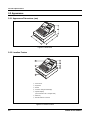
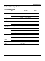

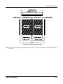


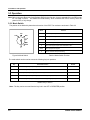
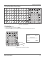
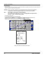
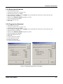
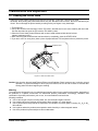


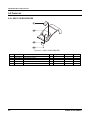
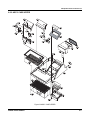

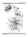


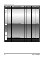
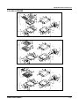
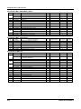
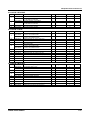

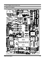
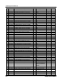
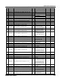
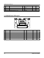


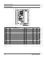
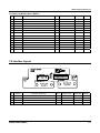


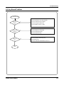
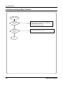
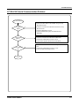

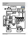
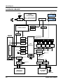
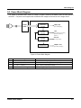

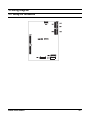
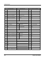


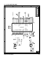
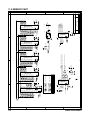

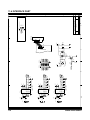
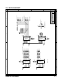
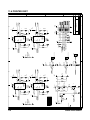
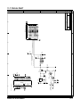


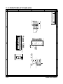

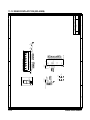
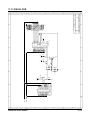
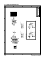
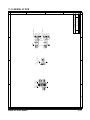


![[SPT-3000] e](http://vs1.manualzilla.com/store/data/005667089_1-a5f3766b3193f6552f250995926a69c5-150x150.png)