1
LogiCORE™
PCI v3.0
Getting Started Guide
UG157 August 31, 2005
v3.0.151
R
R
Xilinx is disclosing this Specification to you solely for use in the development of designs to operate on Xilinx FPGAs. Except as stated herein,
none of the Specification may be copied, reproduced, distributed, republished, downloaded, displayed, posted, or transmitted in any form or
by any means including, but not limited to, electronic, mechanical, photocopying, recording, or otherwise, without the prior written consent
of Xilinx. Any unauthorized use of this Specification may violate copyright laws, trademark laws, the laws of privacy and publicity, and
communications regulations and statutes.
Xilinx does not assume any liability arising out of the application or use of the Specification; nor does Xilinx convey any license under its
patents, copyrights, or any rights of others. You are responsible for obtaining any rights you may require for your use or implementation of
the Specification. Xilinx reserves the right to make changes, at any time, to the Specification as deemed desirable in the sole discretion of
Xilinx. Xilinx assumes no obligation to correct any errors contained herein or to advise you of any correction if such be made. Xilinx will not
assume any liability for the accuracy or correctness of any engineering or technical support or assistance provided to you in connection with
the Specification.
THE SPECIFICATION IS PROVIDED “AS IS" WITH ALL FAULTS, AND THE ENTIRE RISK AS TO ITS FUNCTION AND
IMPLEMENTATION IS WITH YOU. YOU ACKNOWLEDGE AND AGREE THAT YOU HAVE NOT RELIED ON ANY ORAL OR WRITTEN
INFORMATION OR ADVICE, WHETHER GIVEN BY XILINX, OR ITS AGENTS OR EMPLOYEES. XILINX MAKES NO OTHER
WARRANTIES, WHETHER EXPRESS, IMPLIED, OR STATUTORY, REGARDING THE SPECIFICATION, INCLUDING ANY
WARRANTIES OF MERCHANTABILITY, FITNESS FOR A PARTICULAR PURPOSE, TITLE, AND NONINFRINGEMENT OF THIRDPARTY RIGHTS.
IN NO EVENT WILL XILINX BE LIABLE FOR ANY CONSEQUENTIAL, INDIRECT, EXEMPLARY, SPECIAL, OR INCIDENTAL DAMAGES,
INCLUDING ANY LOST DATA AND LOST PROFITS, ARISING FROM OR RELATING TO YOUR USE OF THE SPECIFICATION, EVEN IF
YOU HAVE BEEN ADVISED OF THE POSSIBILITY OF SUCH DAMAGES. THE TOTAL CUMULATIVE LIABILITY OF XILINX IN
CONNECTION WITH YOUR USE OF THE SPECIFICATION, WHETHER IN CONTRACT OR TORT OR OTHERWISE, WILL IN NO EVENT
EXCEED THE AMOUNT OF FEES PAID BY YOU TO XILINX HEREUNDER FOR USE OF THE SPECIFICATION. YOU ACKNOWLEDGE
THAT THE FEES, IF ANY, REFLECT THE ALLOCATION OF RISK SET FORTH IN THIS AGREEMENT AND THAT XILINX WOULD NOT
MAKE AVAILABLE THE SPECIFICATION TO YOU WITHOUT THESE LIMITATIONS OF LIABILITY.
The Specification is not designed or intended for use in the development of on-line control equipment in hazardous environments requiring
fail-safe controls, such as in the operation of nuclear facilities, aircraft navigation or communications systems, air traffic control, life support,
or weapons systems (“High-Risk Applications”). Xilinx specifically disclaims any express or implied warranties of fitness for such High-Risk
Applications. You represent that use of the Specification in such High-Risk Applications is fully at your risk.
© 2005 Xilinx, Inc. All rights reserved. XILINX, the Xilinx logo, and other designated brands included herein are trademarks of Xilinx, Inc. All
other trademarks are the property of their respective owners.
PCI v3.0.151 Getting Started Guide
UG157 August 31, 2005
The following table shows the revision history for this document.
Version
Revision
06/01/00
1.0
Initial Xilinx release.
06/15/00
1.1
Accumulated miscellaneous updates and bug fixes.
07/26/00
1.2
Accumulated miscellaneous updates and bug fixes.
08/28/00
1.3
Fine tuning of text frame and paragraph format spacings.
04/11/01
2.0
Revised formats to take advantage of FrameMaker 6.0 book features.
05/02/01
2.1
Master page changes.
07/11/01
2.2
Accumulated miscellaneous updates and bug fixes.
04/04/02
2.2.1
Updated trademarks page in ug000_title.fm.
PCI v3.0.151 Getting Started Guide
UG157 August 31, 2005
www.xilinx.com
Version
06/24/02
3.0
Revision
Initial Xilinx release of corporate-wide common template set, used for User Guides,
Tutorials, Release Notes, Manuals, and other lengthy, multiple-chapter documents
created by both CMP and ITP. See related documents for further information.
Descriptions for revisions prior to v3.0 have been abbreviated. For a full summary of revision
changes prior to v3.0, refer to v2.2.1 template set.
10/30/02
3.1
Updated spelling of RocketIO and SelectIO trademarks in ug000_title.fm per 10/09/02
broadcast email announcement. Also updated file version number and date.
12/06/02
3.2
Fixed all instances of old character formats in header/footer in Master pages.
01/20/03
3.3
Revised copyright date in ug000_title.fm to 2003. Changed all instances of “Manual” in
ug000_preface.fm to “Guide”. Added PDF Information format under Format →
Document → PDF Setup...
02/06/03
3.4
Added paragraph formats GlossBulleted, GlossNumbered, and GlossNumberedCont.
02/25/03
3.4.1
03/25/03
3.5
• Corrected Reference Page identification problem that prevented the IX (index)
Reference page from taking control of Index formatting.
• Modified paragraph tags Level1IX through Level3IX (index entries) to provide a
more uniform appearance and enhance clarity.
• Removed <Italic> attribute from Heading2TOC special string on Reference pages.
• Changed autonumbering properties of FigureTitle and TableTitle to remove chapter
number and hyphen.
04/30/03
3.5.1
Updated Additional Resources table in Preface to give correct URL to data sheets index
page instead of to obsolete Programmable Logic Data Book page.
11/11/04
3.5.2
Added installation and licensing chapter; updated to current template.
12/01/04
3.6
Updated to include Virtex-4 information.
3/7/05
3.7
Updated to ISE 7.1i and build number 3.0.145.
5/13/05
4.0
Updated to build 3.0.150 and Xilinx tools 7.1i SP2.
8/31/05
5.0
Updated to build 3.0.151 and Xilinx tools 7.1i SP4.
Minor clean-ups and corrections.
www.xilinx.com
PCI v3.0.151 Getting Started Guide
UG157 August 31, 2005
PCI v3.0.151 Getting Started Guide
UG157 August 31, 2005
www.xilinx.com
Table of Contents
Preface: About This Guide
Guide Contents . . . . . . . . . . . . . . . . . . . . . . . . . . . . . . . . . . . . . . . . . . . . . . . . . . . . . . . 7
Additional Resources . . . . . . . . . . . . . . . . . . . . . . . . . . . . . . . . . . . . . . . . . . . . . . . . . 8
Conventions . . . . . . . . . . . . . . . . . . . . . . . . . . . . . . . . . . . . . . . . . . . . . . . . . . . . . . . . . . 8
Typographical . . . . . . . . . . . . . . . . . . . . . . . . . . . . . . . . . . . . . . . . . . . . . . . . . . . . . . . . . . . . . 8
Online Document . . . . . . . . . . . . . . . . . . . . . . . . . . . . . . . . . . . . . . . . . . . . . . . . . . . . . . . . . . 9
Chapter 1: Getting Started
About the Example Design . . . . . . . . . . . . . . . . . . . . . . . . . . . . . . . . . . . . . . . . . . .
Additional Documentation . . . . . . . . . . . . . . . . . . . . . . . . . . . . . . . . . . . . . . . . . . . .
Technical Support . . . . . . . . . . . . . . . . . . . . . . . . . . . . . . . . . . . . . . . . . . . . . . . . . . .
Feedback . . . . . . . . . . . . . . . . . . . . . . . . . . . . . . . . . . . . . . . . . . . . . . . . . . . . . . . . . . .
11
11
12
12
PCI Interface Core . . . . . . . . . . . . . . . . . . . . . . . . . . . . . . . . . . . . . . . . . . . . . . . . . . . . . . . . 12
Document . . . . . . . . . . . . . . . . . . . . . . . . . . . . . . . . . . . . . . . . . . . . . . . . . . . . . . . . . . . . . . . 12
Chapter 2: Installing and Licensing the Core
System Requirements . . . . . . . . . . . . . . . . . . . . . . . . . . . . . . . . . . . . . . . . . . . . . . . . 13
Installing the Core . . . . . . . . . . . . . . . . . . . . . . . . . . . . . . . . . . . . . . . . . . . . . . . . . . . 13
CORE Generator IP Updates Installer . . . . . . . . . . . . . . . . . . . . . . . . . . . . . . . . . . . . . . . 14
Manual Installation: CORE Generator IP Update . . . . . . . . . . . . . . . . . . . . . . . . . . . . . . 14
Direct Download of Standalone Core . . . . . . . . . . . . . . . . . . . . . . . . . . . . . . . . . . . . . . . . 15
Licensing Options . . . . . . . . . . . . . . . . . . . . . . . . . . . . . . . . . . . . . . . . . . . . . . . . . . . 16
Evaluation . . . . . . . . . . . . . . . . . . . . . . . . . . . . . . . . . . . . . . . . . . . . . . . . . . . . . . . . . . . . . . . 16
Full . . . . . . . . . . . . . . . . . . . . . . . . . . . . . . . . . . . . . . . . . . . . . . . . . . . . . . . . . . . . . . . . . . . . . 16
Direct Download . . . . . . . . . . . . . . . . . . . . . . . . . . . . . . . . . . . . . . . . . . . . . . . . . . . . . . . . . 16
Installing Your License File . . . . . . . . . . . . . . . . . . . . . . . . . . . . . . . . . . . . . . . . . . . 17
Chapter 3: Family Specific Considerations
Design Support . . . . . . . . . . . . . . . . . . . . . . . . . . . . . . . . . . . . . . . . . . . . . . . . . . . . . .
Device Initialization . . . . . . . . . . . . . . . . . . . . . . . . . . . . . . . . . . . . . . . . . . . . . . . . . .
Bus Width Detection . . . . . . . . . . . . . . . . . . . . . . . . . . . . . . . . . . . . . . . . . . . . . . . . .
Datapath Output Clock Enable . . . . . . . . . . . . . . . . . . . . . . . . . . . . . . . . . . . . . . . .
Input Delay Buffers . . . . . . . . . . . . . . . . . . . . . . . . . . . . . . . . . . . . . . . . . . . . . . . . . .
Regional Clock Usage . . . . . . . . . . . . . . . . . . . . . . . . . . . . . . . . . . . . . . . . . . . . . . . .
Bus Clock Usage . . . . . . . . . . . . . . . . . . . . . . . . . . . . . . . . . . . . . . . . . . . . . . . . . . . .
Electrical Compliance . . . . . . . . . . . . . . . . . . . . . . . . . . . . . . . . . . . . . . . . . . . . . . . .
Generating Bitstreams . . . . . . . . . . . . . . . . . . . . . . . . . . . . . . . . . . . . . . . . . . . . . . .
19
29
29
30
30
32
34
35
37
Chapter 4: Functional Simulation
Cadence NC-Verilog. . . . . . . . . . . . . . . . . . . . . . . . . . . . . . . . . . . . . . . . . . . . . . . . . . 39
Model Technology ModelSim . . . . . . . . . . . . . . . . . . . . . . . . . . . . . . . . . . . . . . . . . 40
Verilog . . . . . . . . . . . . . . . . . . . . . . . . . . . . . . . . . . . . . . . . . . . . . . . . . . . . . . . . . . . . . . . . . . 40
VHDL . . . . . . . . . . . . . . . . . . . . . . . . . . . . . . . . . . . . . . . . . . . . . . . . . . . . . . . . . . . . . . . . . . . 41
www.xilinx.com
PCI v3.0.151 Getting Started Guide
UG157 August 31, 2005
Chapter 5: Synthesizing a Design
Synplicity Synplify . . . . . . . . . . . . . . . . . . . . . . . . . . . . . . . . . . . . . . . . . . . . . . . . . . . 43
Verilog . . . . . . . . . . . . . . . . . . . . . . . . . . . . . . . . . . . . . . . . . . . . . . . . . . . . . . . . . . . . . . . . . . 43
VHDL . . . . . . . . . . . . . . . . . . . . . . . . . . . . . . . . . . . . . . . . . . . . . . . . . . . . . . . . . . . . . . . . . . . 48
Exemplar LeonardoSpectrum . . . . . . . . . . . . . . . . . . . . . . . . . . . . . . . . . . . . . . . . . 51
Xilinx XST . . . . . . . . . . . . . . . . . . . . . . . . . . . . . . . . . . . . . . . . . . . . . . . . . . . . . . . . . . . 52
Chapter 6: Implementing a Design
ISE Foundation . . . . . . . . . . . . . . . . . . . . . . . . . . . . . . . . . . . . . . . . . . . . . . . . . . . . . . 53
Chapter 7: Timing Simulation
Cadence NC-Verilog. . . . . . . . . . . . . . . . . . . . . . . . . . . . . . . . . . . . . . . . . . . . . . . . . . 55
Model Technology ModelSim . . . . . . . . . . . . . . . . . . . . . . . . . . . . . . . . . . . . . . . . . 56
Verilog . . . . . . . . . . . . . . . . . . . . . . . . . . . . . . . . . . . . . . . . . . . . . . . . . . . . . . . . . . . . . . . . . . 56
VHDL . . . . . . . . . . . . . . . . . . . . . . . . . . . . . . . . . . . . . . . . . . . . . . . . . . . . . . . . . . . . . . . . . . . 56
PCI v3.0.151 Getting Started Guide
UG157 August 31, 2005
www.xilinx.com
R
Preface
About This Guide
The PCI Getting Started Guide provides information about the LogiCORE™ Peripheral
Component Interconnect (PCI) interface, which provides a fully verified, pre-implemented
PCI bus interface available in both 32-bit and 64-bit versions.
This guide discusses the supported design flows for 32-bit and 64-bit PCI interfaces based
on the Virtex™ and Spartan™ architectures, and provides an example design in both
Verilog-HDL and VHDL.
Guide Contents
This manual contains the following chapters:
•
Chapter 1, “Getting Started” describes the core and related information, including
additional resources, technical support, and submitting feedback to Xilinx.
•
Chapter 2, “Installing and Licensing the Core” provides information about installing
and licensing the core.
•
Chapter 3, “Family Specific Considerations” provides information about design
considerations specific to the PCI interface targeting Virtex and Spartan devices.
•
Chapter 4, “Functional Simulation” describes how to simulate the example design
using the supported functional simulation tools, including Cadence NC-Verilog v5.0
and Model Technology ModelSim v5.7b.
•
Chapter 5, “Synthesizing a Design” how to synthesize the example design using the
supported synthesis tools, including Synplicity Synplify v7.3, Exemplar
LeonardoSpectrum v2003a, and Xilinx XST.
•
Chapter 6, “Implementing a Design” describes how to implement the example design
using the supported FPGA implementation tools included with the ISE Foundation
v7.1i software.
•
Chapter 7, “Timing Simulation” describes how to perform timing simulation using
the supported post-route timing simulation tools, including Cadence NC-Verilog v5.0
and Model Technology ModelSim v5.7b.
PCI v3.0.151 Getting Started Guide
UG157 August 31, 2005
www.xilinx.com
7
R
Preface: About This Guide
Additional Resources
For additional information, go to http://support.xilinx.com. The following table lists
some of the resources you can access from this website. You can also directly access these
resources using the provided URLs.
Resource
Tutorials
Description/URL
Tutorials covering Xilinx design flows, from design entry to
verification and debugging
http://support.xilinx.com/support/techsup/tutorials/index.htm
Answer Browser
Database of Xilinx solution records
http://support.xilinx.com/xlnx/xil_ans_browser.jsp
Application Notes
Descriptions of device-specific design techniques and approaches
http://support.xilinx.com/apps/appsweb.htm
Data Sheets
Device-specific information on Xilinx device characteristics,
including readback, boundary scan, configuration, length count,
and debugging
http://support.xilinx.com/xlnx/xweb/xil_publications_index.jsp
Problem Solvers
Interactive tools that allow you to troubleshoot your design issues
http://support.xilinx.com/support/troubleshoot/psolvers.htm
Tech Tips
Latest news, design tips, and patch information for the Xilinx
design environment
http://www.support.xilinx.com/xlnx/xil_tt_home.jsp
Conventions
Typographical
The following typographical conventions are used in this document:
Convention
8
Meaning or Use
Example
Courier font
Messages, prompts, and
program files that the system
displays
speed grade: - 100
Courier bold
Literal commands you enter in
a syntactical statement
ngdbuild design_name
www.xilinx.com
PCI v3.0.151 Getting Started Guide
UG157 August 31, 2005
R
Conventions
Convention
Meaning or Use
Example
Variables in a syntax
statement for which you must
supply values
ngdbuild design_name
References to other manuals
See the Development
System Reference Guide
for more information.
Emphasis in text
If a wire is drawn so that it
overlaps the pin of a symbol,
the two nets are not
connected.
An optional entry or
parameter. However, in bus
specifications, such as
bus[7:0], they are required.
ngdbuild [option_name]
design_name
A list of items from which you
must choose one or more
lowpwr ={on|off}
Separates items in a list of
choices
lowpwr ={on|off}
Vertical ellipsis
.
.
.
Repetitive material that has
been omitted
IOB #1: Name = QOUT’
IOB #2: Name = CLKIN’
.
.
.
Horizontal ellipsis . . .
Omitted repetitive material
allow block block_name
loc1 loc2 ... locn;
Italic font
Square brackets
Braces
[ ]
{ }
Vertical bar
|
Online Document
The following conventions are used in this document:
Convention
Meaning or Use
Blue text
Cross-reference link to a
location in the current
document
Blue, underlined text
Hyperlink to a website (URL)
PCI v3.0.151 Getting Started Guide
UG157 August 31, 2005
www.xilinx.com
Example
See “Additional Resources”
for details.
See “Title Formats” in Chapter
1 for details.
Go to http://www.xilinx.com
for the latest speed files.
9
R
10
Preface: About This Guide
www.xilinx.com
PCI v3.0.151 Getting Started Guide
UG157 August 31, 2005
R
Chapter 1
Getting Started
The PCI interface provides a fully verified, pre-implemented PCI bus interface available in
both 32-bit and 64-bit versions with support for operation at 33 MHz and 66 MHz. This
guide defines the supported design flows for both the 32-bit and 64-bit interfaces targeting
devices based on the Virtex and Spartan architectures. In addition, an example design is
provided in both Verilog-HDL and VHDL that lets you simulate, synthesize, and
implement the interface to understand the PCI design flow.
About the Example Design
The example design is a simple user application provided as a training tool and design
flow test. The example design consists of the user application Ping, and supporting files for
simulation and implementation. The PCI32 interface ships with the ping32 design, and the
PCI64 interface ships with the ping64 design. The examples in this document reference
ping64. If you are using the 32-bit core, substitute ping32 for ping64.
The Ping design includes a testbench capable of generating simple read and write
transactions. This stimulation generation capability is used to set up the configuration
space of the design, and then perform some simple transactions. In addition, a special
configuration file is provided, and the testbench makes assumptions about the size and
number of base address registers used.
Users may change the core options related to implementation, that is, the options that
relate to the selected FPGA architecture. However, users must not change core options that
alter the functional behavior of the PCI core; such changes cause unpredictable results in
the simulation of the example design. For custom designs, users have the flexibility to
change the PCI core configuration as described in the PCI v3.0 User Guide.
Step-by-step instructions using supported design tools are provided to simulate,
synthesize, and implement the Ping example design.
Additional Documentation
For more information about the PCI interface core, see the following documents, located on
the PCI product page:
•
PCI Release Notes
•
PCI User Guide
Further information is available in the Mindshare PCI System Architecture text, and the
PCI Local Bus Specification, available from the PCI Special Interest Group site.
PCI v3.0.151 Getting Started Guide
UG157 August 31, 2005
www.xilinx.com
11
R
Chapter 1: Getting Started
Technical Support
For technical support, visit www.xilinx.com/support. Questions are routed to a team of
engineers with expertise using the PCI interface.
Xilinx provides technical support for use of this product as described in the PCI User Guide
and the PCI Getting Started Guide. Xilinx cannot guarantee timing, functionality, or support
of this product for designs that do not follow these guidelines.
Feedback
Xilinx welcomes comments and suggestions about the PCI interface core and the
documentation supplied with the core.
PCI Interface Core
For comments and suggestions about the PCI interface core, please submit a webcase from
www.xilinx.com/support. Be sure to include the following information:
•
Product name
•
Core version number
•
Explanation of your comments
Document
For comments or suggestions about this document, please submit a webcase from
www.xilinx.com/support. Be sure to include the following information:
12
•
Document title and number
•
Page number(s) to which your comments refer
•
Explanation of your comments
www.xilinx.com
PCI v3.0.151 Getting Started Guide
UG157 August 31, 2005
R
Chapter 2
Installing and Licensing the Core
This chapter provides instructions for installing and obtaining a license for the PCI
interface core, which you must do before using it in your designs. The PCI core is provided
under the terms of the Xilinx LogiCORE Site License Agreement or the Xilinx LogiCORE
Project License Agreement, which conform to the terms of the SignOnce IP License/Project
standard defined by the Common License Consortium. Purchase of the PCI core entitles
you to technical support and access to updates for a period of one year.
Important note: Please visit the PCI/PCI-X lounge frequently to make sure that you are
using the latest version of the core. You can always download the most up-to-date version
of the core from the product lounge.
System Requirements
Windows
•
Windows® 2000 Professional (Service Pack 2-4)
•
Windows XP Home (Service Pack 1); Windows XP Professional (Service Pack 1)
Solaris/Linux
•
Sun Solaris™ 8/9
•
Red Hat® Enterprise Linux 3.0 (32-bit and 64-bit)
Software
•
ISE 7.1i or higher (Service Pack 4)
Note: If necessary, ISE 7.1i Service Packs can be downloaded from
http://www.xilinx.com/xlnx/xil_sw_updates_home.jsp?update=ip&software=7.1i
Installing the Core
You can install the PCI core in three ways:
•
Using the CORE Generator IP Updates Installer, which displays a list of compatible
updates from which you select the desired core or core update
•
Performing a manual installation of the appropriate ISE CORE Generator IP Update
•
Directly downloading it from the PCI lounge, a secured area of the PCI product page
Note: The first two methods apply to configurations of the core delivered through the
CORE Generator. To access the CORE Generator full product license or to download the
core directly from the PCI lounge, you must purchase the core.
PCI v3.0.151 Getting Started Guide
UG157 August 31, 2005
www.xilinx.com
13
R
Chapter 2: Installing and Licensing the Core
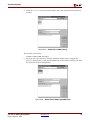
CORE Generator IP Updates Installer
1.
From the CORE Generator main GUI, choose Tools > Updates Installer to start the
Updates Installer.
2.
If prompted for a proxy host, contact your administrator to determine the proxy host
address and port number you need to get through your firewall.
3.
Select 7.1i_IP_Update3 from the list of updates in the Available Packages panel.
4.
Click Add To Install Queue to add the update ZIP file to the install queue.
5.
Do one of the following:
6.
•
If prompted to enter a log-in name and password, enter your Xilinx log-in and
password.
•
If you are new to Xilinx, click Create an Account and follow the instructions to
create an account. (After creating an account, you will be redirected to the page to
download the core.)
Click Install All Packages from Queue to download the update.
After downloading the update, the Updates Installer terminates the CORE Generator
session and installs the downloaded archive. After the download is complete, you can
restart the CORE Generator.
7.
To confirm the installation, check the following file:
C:\Xilinx\coregen\install\install_history.
Note: This step assumes your Xilinx software is installed in C:\Xilinx.
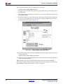
Manual Installation: CORE Generator IP Update
1.
Close the CORE Generator application if it is running.
2.
Download the IP Update ZIP file (Windows) or tar.gz file (UNIX) from the following
location and save it to a temporary directory:
http://www.xilinx.com/xlnx/xil_sw_updates_home.jsp?update=ip&software=7.1i
3.
14
•
If prompted to enter a log-in name and password, enter your Xilinx log-in and
password.
•
If you are new to Xilinx, click Create an Account and follow the instructions to
create an account.
Do one of the following:
•
For Windows, unpack the ZIP file using WinZip 7.0 SR-1 or later.
•
For UNIX, Xilinx recommends that you unpack the tar.gz file using the UNIX
command line utilities gunzip and tar. WinZip and GNU tar are not
recommended due to differences in the way they handle files with long path
names. Please see Xilinx Answer 11162 for details.
4.
Extract the ZIP file (ise_71i_ip_update3.zip) or tar.gz (ise_71i_ip_update3.tar.gz)
archive to the root directory of your Xilinx software installation. Allow the extractor
utility to overwrite all existing files and maintain the directory structure defined in the
archive.
5.
To verify the root directory of your Xilinx installation, do one of the following:
•
For Windows: Type echo%XILINX% from a DOS prompt.
•
For Unix: If you have already installed the Xilinx ISE software, the Xilinx variable
defined by your set-up script identifies the location of the Xilinx installation
directory. After sourcing the Xilinx set-up script, type echo $XILINX to determine
www.xilinx.com
PCI v3.0.151 Getting Started Guide
UG157 August 31, 2005
R
Installing the Core
the location of the Xilinx installation. Note that you may need system
administrator privileges to install the update.
6.
Confirm the directory structure in one of the following ways:
•
For Windows:
<Xilinx_root_directory>\coregen\ip\xilinx\network_ip1_h\com\xilinx
\ip\pci64_v30151
•
For UNIX:
<Xilinx_root_directory>/coregen/ip/xilinx/network_ip1_h/com/xilinx
/ip/pci64_v30151
If you do not see this directory structure, recheck the directory to which you extracted
the archive and try again.
7.
Restart the CORE Generator. During start-up, the CORE Generator automatically
detects new versions of IP available in your installation and lets you specify which IP
customizers (cores) will be visible in your current CORE Generator project.
8.
Choose one of the following options:
9.
•
Display only the latest versions for all cores in the catalog
•
Update the catalog view to add only new cores to the display
•
Make a Custom selection of visible cores in your current project
Determine if the installation was successful by verifying that the new cores are visible
in the CORE Generator GUI.
10. If the new cores aren’t visible, return to Step 6 to verify the directory structure. If the
directory structure is incorrect, return Step 4 to verify that the directory was extracted
to the correct location.
For additional assistance installing the IP Update, contact the Xilinx Hotline.
Direct Download of Standalone Core
The PCI core can be downloaded from the Xilinx website and used outside of the CORE
Generator by downloading a .zip file containing the core and other necessary supporting
files. Note that you must purchase the core to use this option.
1.
After purchase, you will receive a letter containing a serial number, which is used to
register for access to the lounge, a secured area of the PCI product page. Go to
http://www.xilinx.com/products/logicore/lounge/lounge.htm and choose the
appropriate link to gain access to the core you purchased.
2.
From the core’s product page, click Register to register and request access to the
lounge. Xilinx will review your access request and typically grants access to the lounge
in 48 hours. (Contact Xilinx Customer Service if you need faster turnaround.)
3.
After you receive confirmation of lounge access, click Access Lounge from the
appropriate PCI product page and log in.
This page lists the current build of the core as well as previous builds. For new designs
or to update an existing design, select the current version of the core.
4.
From the table, select the desired version. A page specific to the version appears.
5.
Click the link to the .zip file to download it. After saving the .zip file, unzip it to the
desired location on your system.
6.
If desired, customize the core settings by following the instructions in Chapter 5,
“Customizing the PCI Interface” of the PCI v3.0 User Guide.
PCI v3.0.151 Getting Started Guide
UG157 August 31, 2005
www.xilinx.com
15
R
Chapter 2: Installing and Licensing the Core
Licensing Options
Evaluation
The method for obtaining an evaluation license is determined by the version of the PCI
core you choose.
•
For the PCI32/33 Virtex™ and Spartan™ core, register on the Xilinx IP Evaluation
page at www.xilinx.com/ipcenter/ipevaluation. From this location, access is granted
and you can generate your own license.
•
For the PCI 64/66 core, please contact your locate FAE to request a Full System
Hardware Evaluation license key.
Full
The Full license is provided when you purchase the core, and provides full access to all
core functionality both in simulation and in hardware, including:
•
Gate-level functional simulation support
•
Back annotated gate-level simulation support
•
Full implementation support including place and route and bitstream generation
•
Full functionality in the programmed device with no time-outs
Obtaining a Full License
After purchase, a full license for the Xilinx PCI core can be downloaded from the core’s
lounge. To create and download a license file for use with the CORE Generator, do the
following:
1.
After purchase, you will receive a letter containing a serial number, which is used to
register for access to the lounge, a secured area of the PCI product page. Go to
http://www.xilinx.com/products/logicore/lounge/lounge.htm and choose the
appropriate link to gain access to core.
2.
From the product page, click Register to register and request access to the lounge.
Xilinx will review your access request and typically grants access to the lounge in
48 hours. (Contact Xilinx Customer Service if you need faster turnaround.)
3.
After receiving confirmation of lounge access, click Access Lounge from the PCI
product page and log in.
4.
From the lounge, a link is available at the top of the initial page allowing you to
generate a license. Click this link and follow the instructions to fill out the license
request form; then click Submit to generate the license. An e-mail containing license
and installation instructions will be sent to you immediately.
Direct Download
A CORE Generator license is not required when performing a direct download of PCI-X
core, as described in “Direct Download of Standalone Core,” page 15.
16
www.xilinx.com
PCI v3.0.151 Getting Started Guide
UG157 August 31, 2005
R
Installing Your License File
Installing Your License File
After selecting a license option, an email will be sent to you that includes instructions for
installing your license file. In addition, information about advanced licensing options and
technical support is provided.
PCI v3.0.151 Getting Started Guide
UG157 August 31, 2005
www.xilinx.com
17
R
18
Chapter 2: Installing and Licensing the Core
www.xilinx.com
PCI v3.0.151 Getting Started Guide
UG157 August 31, 2005
R
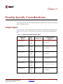
Chapter 3
Family Specific Considerations
This chapter provides important design information specific to the PCI interface targeting
Virtex and Spartan devices.
Design Support
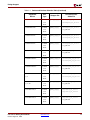
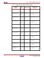
Table 3-1 provides a list of supported device and interface combinations. Each entry in the
table consists of a device, a bus interface type, and two or three specific implementation
files.
Table 3-1:
Device and Interface Selection Table
Supported
Device
2S100-FG456-6C
Bus
Type
33 MHz
Wrapper File
pcim_lc_33_5_s
Constraints File/
Guide File
2s100fg456_64_33.ucf
no guide file
5.0V
64-bit
2S100-FG456-6C
33 MHz
pcim_lc_33_3_s
2s100fg456_64_33.ucf
no guide file
3.3V
64-bit
2S150-FG456-6C
33 MHz
pcim_lc_33_5_s
2s150fg456_64_33.ucf
no guide file
5.0V
64-bit
2S150-FG456-6C
33 MHz
pcim_lc_33_3_s
2s150fg456_64_33.ucf
no guide file
3.3V
64-bit
2S150-FG456-6C
66 MHz
pcim_lc_66_3_d
3.3V
2s150fg456_64_66.ucf
2s150fg456_64_66.ncd
64-bit
2S200-FG456-6C
33 MHz
5.0V
pcim_lc_33_5_s
2s200fg456_64_33.ucf
no guide file
64-bit
PCI v3.0.151 Getting Started Guide
UG157 August 31, 2005
www.xilinx.com
19
R
Chapter 3: Family Specific Considerations
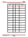
Table 3-1:
Device and Interface Selection Table (Continued)
Supported
Device
2S200-FG456-6C
Bus
Type
33 MHz
Wrapper File
pcim_lc_33_3_s
3.3V
Constraints File/
Guide File
2s200fg456_64_33.ucf
no guide file
64-bit
2S200-FG456-6C
66 MHz
pcim_lc_66_3_d
3.3V
2s200fg456_64_66.ucf
2s200fg456_64_66.ncd
64-bit
2S100E-FG456-6C
33 MHz
pcim_lc_33_3_s
3.3V
2s100efg456_64_33.ucf
no guide file
64-bit
2S150E-FG456-6C
33 MHz
pcim_lc_33_3_s
3.3V
2s150efg456_64_33.ucf
no guide file
64-bit
2S200E-FG456-6C
33 MHz
pcim_lc_33_3_s
3.3V
2s200efg456_64_33.ucf
no guide file
64-bit
2S300E-FG456-6C
33 MHz
pcim_lc_33_3_s
3.3V
2s300efg456_64_33.ucf
no guide file
64-bit
2S300E-FG456-6C
66 MHz
pcim_lc_66_3_d
3.3V
2s300efg456_64_66.ucf
2s300efg456_64_66.ncd
64-bit
V100E-BG352-6C
33 MHz
pcim_lc_33_3_s
3.3V
v100ebg352_64_33.ucf
no guide file
64-bit
V300-BG432-6C
66 MHz
pcim_lc_66_3_d
3.3V
v300bg432_64_66.ucf
v300bg432_64_66.ncd
64-bit
V300-BG432-5C
33 MHz
pcim_lc_33_5_s
5.0V
v300bg432_64_33.ucf
no guide file
64-bit
V300-BG432-5C
33 MHz
3.3V
pcim_lc_33_3_s
v300bg432_64_33.ucf
no guide file
64-bit
20
www.xilinx.com
PCI v3.0.151 Getting Started Guide
UG157 August 31, 2005
R
Design Support
Table 3-1:
Device and Interface Selection Table (Continued)
Supported
Device
V300E-BG432-6C
Bus
Type
Wrapper File
66 MHz
pcim_lc_66_3_d
3.3V
Constraints File/
Guide File
v300ebg432_64_66.ucf
v300ebg432_64_66.ncd
64-bit
V300E-BG432-6C
33 MHz
pcim_lc_33_3_s
3.3V
v300ebg432_64_33.ucf
no guide file
64-bit
V1000-FG680-6C
66 MHz
pcim_lc_66_3_d
3.3V
v1000fg680_64_66.ucf
v1000fg680_64_66.ncd
64-bit
V1000-FG680-5C
33 MHz
pcim_lc_33_5_s
5.0V
v1000fg680_64_33.ucf
no guide file
64-bit
V1000-FG680-5C
33 MHz
pcim_lc_33_3_s
3.3V
v1000fg680_64_33.ucf
no guide file
64-bit
V1000E-FG680-6C
66 MHz
pcim_lc_66_3_d
3.3V
v1000efg680_64_66.ucf
v1000efg680_64_66.ncd
64-bit
V1000E-FG680-6C
33 MHz
pcim_lc_33_3_s
3.3V
v1000efg680_64_33.ucf
no guide file
64-bit
2V1000-FG456-5
C/I
66 MHz
pcim_lc_66_3_s
3.3V
2v1000fg456_64_66.ucf
2v1000fg456_64_66.ncd
64-bit
2V1000-FG456-4
C/I /M
33 MHz
pcim_lc_33_3_s
3.3V
2v1000fg456_64_33.ucf
no guide file
64-bit
2VP7-FF672-6C/I
66 MHz
pcim_lc_66_3_s
3.3V
2vp7ff672_64_66.ucf
2vp7ff672_64_66.ncd
64-bit
2VP7-FF672-5C/I
33 MHz
3.3V
pcim_lc_33_3_s
2vp7ff672_64_33.ucf
no guide file
64-bit
PCI v3.0.151 Getting Started Guide
UG157 August 31, 2005
www.xilinx.com
21
R
Chapter 3: Family Specific Considerations
Table 3-1:
Device and Interface Selection Table (Continued)
Supported
Device
2VP20-FF1152-6C/I
Bus
Type
66 MHz
Wrapper File
pcim_lc_66_3_s
3.3V
Constraints File/
Guide File
2vp20ff1152_64_66.ucf
2vp20ff1152_64_66.ncd
64-bit
2VP20-FF1152-5C/I
33 MHz
pcim_lc_33_3_s
3.3V
2vp20ff1152_64_33.ucf
no guide file
64-bit
2VP30-FF1152-6C/I
66 MHz
pcim_lc_66_3_s
3.3V
2vp30ff1152_64_66.ucf
2vp30ff1152_64_66.ncd
64-bit
2VP30-FF1152-5C/I
33 MHz
pcim_lc_33_3_s
3.3V
2vp30ff1152_64_33.ucf
no guide file
64-bit
2VP40-FF1152-6C/I
66 MHz
pcim_lc_66_3_s
3.3V
2vp40ff1152_64_66.ucf
2vp40ff1152_64_66.ncd
64-bit
2VP40-FF1152-5C/I
33 MHz
pcim_lc_33_3_s
3.3V
2vp40ff1152_64_33.ucf
no guide file
64-bit
2VP50-FF1152-6C/I
66 MHz
pcim_lc_66_3_s
3.3V
2vp50ff1152_64_66.ucf
2vp50ff1152_64_66.ncd
64-bit
2VP50-FF1152-5C/I
33 MHz
pcim_lc_33_3_s
3.3V
2vp50ff1152_64_33.ucf
no guide file
64-bit
3S1000-FG456-4C/I
33 MHz
pcim_lc_33_3_s
3.3V
3s1000fg456_64_33.ucf
no guide file
64-bit
3S1200E-FG400-4C/I
33 MHz
pcim_lc_33_3_s
3.3V
3s1200efg400_64_33.ucf
no guide file
64-bit
4VLX25-FF668-10C/I
global clock
33 MHz
3.3V
pcim_lc_33_3_g
4vlx25ff668_64_33g.ucf
no guide file
64-bit
22
www.xilinx.com
PCI v3.0.151 Getting Started Guide
UG157 August 31, 2005
R
Design Support
Table 3-1:
Device and Interface Selection Table (Continued)
Supported
Device
4VSX35-FF668-10C/I
global clock
Bus
Type
Wrapper File
Constraints File/
Guide File
33 MHz
pcim_lc_33_3_g
4vsx35ff668_64_33g.ucf
3.3V
no guide file
64-bit
4VFX20-FF672-10C/I
global clock
33 MHz
pcim_lc_33_3_g
3.3V
4vfx20ff672_64_33g.ucf
no guide file
64-bit
4VLX25-FF668-10C/I
regional clock
33 MHz
pcim_lc_33_3_r
3.3V
4vlx25ff668_64_33r.ucf
no guide file
64-bit
4VSX35-FF668-10C/I
regional clock
33 MHz
pcim_lc_33_3_r
3.3V
4vsx35ff668_64_33r.ucf
no guide file
64-bit
4VFX20-FF672-10C/I
regional clock
33 MHz
pcim_lc_33_3_r
3.3V
4vfx20ff672_64_33r.ucf
no guide file
64-bit
4VLX25-FF668-11C/I
regional clock
66 MHz
pcim_lc_66_3_r
3.3V
4vlx25ff668_64_66r.ucf
no guide file
64-bit
4VSX35-FF668-11C/I
regional clock
66 MHz
pcim_lc_66_3_r
3.3V
4vsx35ff668_64_66r.ucf
no guide file
64-bit
4VFX20-FF672-11C/I
regional clock
66 MHz
pcim_lc_66_3_r
3.3V
4vlx20ff672_64_66r.ucf
no guide file
64-bit
2S30-PQ208-5C
33 MHz
pcim_lc_33_5_s
5.0V
2s030pq208_32_33.ucf
no guide file
32-bit
2S30-PQ208-5C
33 MHz
pcim_lc_33_3_s
3.3V
2s030pq208_32_33.ucf
no guide file
32-bit
2S50-PQ208-5C
33 MHz
5.0V
pcim_lc_33_5_s
2s050pq208_32_33.ucf
no guide file
32-bit
PCI v3.0.151 Getting Started Guide
UG157 August 31, 2005
www.xilinx.com
23
R
Chapter 3: Family Specific Considerations
Table 3-1:
Device and Interface Selection Table (Continued)
Supported
Device
2S50-PQ208-5C
Bus
Type
33 MHz
Wrapper File
pcim_lc_33_3_s
3.3V
Constraints File/
Guide File
2s050pq208_32_33.ucf
no guide file
32-bit
2S100-PQ208-5C
33 MHz
pcim_lc_33_5_s
5.0V
2s100pq208_32_33.ucf
no guide file
32-bit
2S100-PQ208-5C
33 MHz
pcim_lc_33_3_s
3.3V
2s100pq208_32_33.ucf
no guide file
32-bit
2S150-PQ208-5C
33 MHz
pcim_lc_33_5_s
5.0V
2s150pq208_32_33.ucf
no guide file
32-bit
2S150-PQ208-5C
33 MHz
pcim_lc_33_3_s
3.0V
2s200pq208_32_33.ucf
no guide file
32-bit
2S200-PQ208-5C
33 MHz
pcim_lc_33_5_s
5.0V
2s200pq208_32_33.ucf
no guide file
32-bit
2S200-PQ208-5C
33 MHz
pcim_lc_33_3_s
3.3V
2s150pq208_32_33.ucf
no guide file
32-bit
2S50E-PQ208-6C
33 MHz
pcim_lc_33_3_s
3.3V
2s050epq208_32_33.ucf
no guide file
32-bit
2S100E-PQ208-6C
33 MHz
pcim_lc_33_3_s
3.3V
2s100epq208_32_33.ucf
no guide file
32-bit
2S150E-PQ208-6C
33 MHz
pcim_lc_33_3_s
3.3V
2s150epq208_32_33.ucf
no guide file
32-bit
2S200E-PQ208-6C
33 MHz
3.3V
pcim_lc_33_3_s
2s200epq208_32_33.ucf
no guide file
32-bit
24
www.xilinx.com
PCI v3.0.151 Getting Started Guide
UG157 August 31, 2005
R
Design Support
Table 3-1:
Device and Interface Selection Table (Continued)
Supported
Device
2S300E-PQ208-6C
Bus
Type
33 MHz
Wrapper File
pcim_lc_33_3_s
3.3V
Constraints File/
Guide File
2s300epq208_32_33.ucf
no guide file
32-bit
V100E-BG352-6C
33 MHz
pcim_lc_33_3_s
3.3V
v100ebg352_32_33.ucf
no guide file
32-bit
V300-BG432-5C
33 MHz
pcim_lc_33_5_s
5.0V
v300bg432_32_33.ucf
no guide file
32-bit
V300-BG432-5C
33 MHz
pcim_lc_33_3_s
3.3V
v300bg432_32_33.ucf
no guide file
32-bit
V300E-BG432-6C
33 MHz
pcim_lc_33_3_s
3.3V
v300ebg432_32_33.ucf
no guide file
32-bit
V1000-FG680-5C
33 MHz
pcim_lc_33_5_s
5.0 V
v1000fg680_32_33.ucf
no guide file
32-bit
V1000-FG680-5C
33 MHz
pcim_lc_33_3_s
3.3V
v1000fg680_32_33.ucf
no guide file
32-bit
V1000E-FG680-6C
33 MHz
pcim_lc_33_3_s
3.3V
v1000efg680_32_33.ucf
no guide file
32-bit
2V1000-FG456-4
C/I/M
33 MHz
pcim_lc_33_3_s
3.3V
2v1000fg456_32_33.ucf
no guide file
32-bit
2VP7-FF672-5C/I
33 MHz
pcim_lc_33_3_s
3.3V
2vp7ff672_32_33.ucf
no guide file
32-bit
3S1000-FG456-4C/I
33 MHz
3.3V
pcim_lc_33_3_s
3s1000fg456_32_33.ucf
no guide file
32-bit
PCI v3.0.151 Getting Started Guide
UG157 August 31, 2005
www.xilinx.com
25
R
Chapter 3: Family Specific Considerations
Table 3-1:
Device and Interface Selection Table (Continued)
Supported
Device
3S1200E-FG400-4C/I
Bus
Type
33 MHz
Wrapper File
pcim_lc_33_3_s
3.3V
Constraints File/
Guide File
3s1200efg400_32_33.ucf
no guide file
32-bit
V200-FG256-6C
66 MHz
pcim_lc_66_3_d
3.3V
v200fg256_32_66.ucf
v200fg256_32_66.ncd
32-bit
V200E-FG256-6C
66 MHz
pcim_lc_66_3_d
3.3V
v200efg256_32_66.ucf
v200efg256_32_66.ncd
32-bit
V400E-FG676-6C
66 MHz
pcim_lc_66_3_d
3.3V
v400efg676_32_66.ucf
v400efg676_32_66.ncd
32-bit
4VLX25-FF668-10C/I
global clock
33 MHz
pcim_lc_33_3_g
3.3V
4vlx25ff668_32_33g.ucf
no guide file
32-bit
4VSX35-FF668-10C/I
global clock
33 MHz
pcim_lc_33_3_g
3.3V
4vsx35ff668_32_33g.ucf
no guide file
32-bit
4VFX20-FF672-10C/I
global clock
33 MHz
pcim_lc_33_3_g
3.3V
4vfx20ff672_32_33g.ucf
no guide file
32-bit
4VLX25-FF668-10C/I
regional clock
33MHz
pcim_lc_33_3_r
3.3V
4vlx25ff668_32_33r.ucf
no guide file
32-bit
4VSX35-FF668-10C/I
regional clock
33MHz
pcim_lc_33_3_r
3.3V
4vsx35ff668_32_33r.ucf
no guide file
32-bit
4VFX20-FF672-10C/I
regional clock
33MHz
pcim_lc_33_3_r
3.3V
4vfx20ff672_32_33r.ucf
no guide file
32-bit
4VLX25-FF668-11C/I
regional clock
66 MHz
3.3V
pcim_lc_66_3r
4vlx25ff668_32_33r.ucf
no guide file
32-bit
26
www.xilinx.com
PCI v3.0.151 Getting Started Guide
UG157 August 31, 2005
R
Design Support
Table 3-1:
Device and Interface Selection Table (Continued)
Supported
Device
4VSX35-FF668-11C/I
regional clock
Bus
Type
66 MHz
Wrapper File
pcim_lc_66_3r
3.3V
Constraints File/
Guide File
4vsx35ff668_32_33r.ucf
no guide file
32-bit
4VFX20-FF672-11C/I
regional clock
66 MHz
3.3V
pcim_lc_66_3r
4vfx20ff672_32_33r.ucf
no guide file
32-bit
See the product release notes included with the core for a complete directory structure and
file list.
PCI v3.0.151 Getting Started Guide
UG157 August 31, 2005
www.xilinx.com
27
R
Chapter 3: Family Specific Considerations
Wrapper Files
Wrapper files contain an instance of the PCI interface and the instances of all I/O elements
used by the PCI interface. Each wrapper file is specific to a particular PCI bus signaling
environment.
The wrapper files, located in the <Install Path>/hdl/src/wrap directory, are
actually variations of the pcim_lc.hdl file located in the <Install
Path>/hdl/src/xpci directory. When starting a new design, copy the appropriate
wrapper file from the wrap/ directory into the xpci/ directory, and rename it
pcim_lc.hdl.
Constraints Files
The user constraints files contain various constraints required for the PCI interface, and
must always be used while processing a design. Each constraints file is specific to a
particular device and PCI interface—use the appropriate constraints file from the
<Install Path>/hdl/src/ucf directory when processing designs with the Xilinx
implementation tools.
Guide Files
The guide files contain routing information required for high-performance versions of the
PCI interface. Each guide file is specific to a particular device and PCI interface, and must
always be used when required. Guide files are located in the <Install
Path>/hdl/src/guide directory. If a guide file is required, use the appropriate guide
file from the guide directory when processing designs with the Xilinx implementation
tools.
Table 3-2 specifies how many guided components and guided connections are included in
each guide file. See this table after implementation to verify your results.
The example design requires the presence of the default pcim_lc.hdl wrapper file in the
xpci/ directory. If you change this file, you must also change the constraints and guide
files used in the processing scripts.
Table 3-2:
28
Guide File Information
Guide File
Components
Connections
2s150fg456_64_66.ncd
150
134
2s200fg456_64_66.ncd
150
134
2s300efg456_64_66.ncd
214
134
v300bg432_64_66.ncd
214
134
v300ebg432_64_66.ncd
214
134
v1000fg680_64_66.ncd
214
134
v1000efg680_64_66.ncd
214
134
2v1000fg456_64_66.ncd
150
240
2vp7ff672_64_66.ncd
153
246
2vp20ff1152_64_66.ncd
153
246
2vp30ff1152_64_66.ncd
153
246
www.xilinx.com
PCI v3.0.151 Getting Started Guide
UG157 August 31, 2005
R
Device Initialization
Table 3-2:
Guide File Information
Guide File
Components
Connections
2vp40ff1152_64_66.ncd
153
246
2vp50ff1152_64_66.ncd
153
246
v200fg256_32_66.ncd
90
86
v200efg256_32_66.ncd
90
86
v400fg676_32_66.ncd
90
86
Device Initialization
Immediately after FPGA configuration, both the PCI interface and the user application are
initialized by the startup mechanism present in all Virtex and Spartan devices.
During normal operation, the assertion of RST# on the PCI bus reinitializes the PCI
interface and three-states all PCI bus signals. This behavior is fully compliant with the PCI
Local Bus Specification. The PCI interface is designed to correctly handle asynchronous
resets.
Typically, the user application must be initialized each time the PCI interface is initialized.
In this case, use the RST output of the PCI interface as the asynchronous reset signal for the
user application. If part of the user application requires an initialization capability that is
asynchronous to PCI bus resets, simply design the user application with a separate reset
signal.
Note that these reset schemes require the use of routing resources to distribute reset
signals, because the global resource is not used. The use of the global reset resource is not
recommended.
Bus Width Detection
A PCI interface that provides a 64-bit datapath needs to know if it is connected to a 64-bit
bus or a 32-bit bus. The SLOT64 signal is an input to the PCI64 interface for this purpose.
The PCI bus specification provides a mechanism for PCI agents to determine the width of
the bus by sampling the state of the REQ64# signal at the rising edge of RST#.
In embedded systems, where the bus width is known by design, the user application can
simply drive SLOT64 with the appropriate value. Note that SLOT64 must never be driven
with a static value; it should always be driven from the output of a flip-flop.
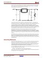
In designs for open systems, the bus width is not known in advance. In this case, include a
separate latch or flip-flop, external to the FPGA, to sample REQ64#. Figure 3-1 shows how
this can be accomplished.
RESISTOR
REQ64#
D
RST#
Figure 3-1:
PCI v3.0.151 Getting Started Guide
UG157 August 31, 2005
Q
SLOT64
C
Sample SLOT64 Generation
www.xilinx.com
29
R
Chapter 3: Family Specific Considerations
Although this technique is not technically compliant with the PCI specification due to the
extra loading on REQ64# and RST#, the use of a large series resistor helps minimize this
effect. The inverter may be pushed into the FPGA.
An alternate method is to push the entire circuit into the FPGA and use the REQ64Q_N and
RST signals provided to the user application. This method requires that the FPGA be fully
configured by the rising edge of RST#.
When SLOT64 is deasserted, the PCI64 interface automatically three-states the 64-bit
extension signals. In this situation, the 64-bit extension signals are undriven, which may
result in additional power consumption by the input buffers.
If the additional power consumption is of concern due to design requirements, consider
changing the “Disabled Extension Drive” option in the HDL configuration file. This
option, when enabled, forces the PCI64 interface to actively drive the extension signals
when SLOT64 is deasserted.
Note: Although this option may reduce power consumption, it creates an electrically
objectionable situation. When a 64-bit card is installed in a 32-bit slot, the 64-bit bus
extension is floating in free space and unprotected from roaming screwdrivers.
Datapath Output Clock Enable
The PCI interface targeting Virtex devices uses one of the following methods to generate
and distribute the datapath output clock enable signal:
•
Specialized device resources: the PCIIOBs, PCILOGIC, and PCI_CE
•
Generic device resources: IOBs, LUTs, and general purpose routing
The specialized device resources offer higher and more predictable performance.
However, they constrain the PCI interface to the left or right sides of the FPGA device, and
limit the number of PCI interface instances to two. The generic device resources, while
lower performance and less predictable, offer greater flexibility.
To summarize, the generic device resources must be used in the following cases:
•
When the target device is Virtex-II, Virtex-II Pro, Virtex-4, or Spartan-3
•
Where more than two instances of the interface are required
•
When the interface cannot be located on the left or right side
To disable the use of specialized device resources, edit the HDL configuration file and set
the CFG[251] bit to logic one. You must set CFG[251] to logic one to target a Virtex-II,
Virtex-II Pro, Virtex-4, or Spartan-3 device. Use of this option with other devices is not
supported, and is incompatible with the provided constraint and guide files.
Input Delay Buffers
Input delay buffers are used to provide guaranteed hold time on all bus inputs. Where
possible, the PCI interface targeting Virtex devices uses input delay elements present in the
30
www.xilinx.com
PCI v3.0.151 Getting Started Guide
UG157 August 31, 2005
R
Input Delay Buffers
IOBs of the FPGA device. The use of these delay buffers is selected through the
implementation specific constraints file
Table 3-3:
Delay Buffer Settings
Implementation
Delay Setting
Virtex, Virtex-E (All)
“0000”
Spartan-II, Spartan-IIE (All)
“0000”
Virtex-II, Spartan-3, Spartan-3E (All)
“0000”
Virtex-II Pro (All 33 MHz)
“0000”
Virtex-II Pro (All 66 MHz)
“0001”
Virtex-4 (Global Clock)
“0000”
Virtex-4 (Regional Clock)
“1000”
Some implementations use alternate delay buffers, selected via the CFG[248:245] bits in
the HDL configuration file. Table 3-3 shows the required settings for CFG[248:245] in
the HDL configuration file.
You must set CFG[248:245] appropriately for the selected implementation. While the
default setting is used for most implementations, failure to match the settings to the
selected implementation may result in hardware failures.
Virtex-4 implementations make use of the new IDELAY input delay buffer primitives. An
IDELAY input delay buffer is a calibrated and adjustable delay line. This delay mechanism
provides superior performance over the legacy input delay buffers. Be sure to observe the
settings shown in Table 3-3 and use the appropriate constraints file for the design.
Designs that use IDELAY primitives also require the use of the IDELAYCTRL primitive.
The function of the IDELAYCTRL primitive is to calibrate the IDELAY delay lines. To
perform this calibration, the IDELAYCTRL primitive requires a 200 MHz input clock. The
design and wrapper files for use with reference clocks contain IDELAY instances,
IDELAYCTRL instances, and an additional input, RCLK, for a 200 MHz reference clock
from an I/O pin. This reference clock is distributed to all applicable IDELAYCTRL
primitives using a global clock buffer.
It is important to note that there is some flexibility in the origin, generation, and use of this
200 MHz reference clock. The provided design and wrapper files represent a trivial case
that can may be modified to suit specific design requirements:
•
For designs requiring IDELAY and IDELAYCTRL for other IP cores, or custom user
logic, the 200 MHz reference clock can be shared. It is possible to tap the reference
clock in the wrapper file, after it is driven by the global buffer. This signal may be
used by other IDELAY and IDELAYCTRL instances.
•
For designs that already have a 200 MHz reference clock distributed on a global clock
buffer, this clock can be shared. The wrapper file can be modified to remove the
external I/O pin and the global clock buffer instance. Simply tap the existing 200 MHz
clock signal and bring it into the wrapper file for the interface to use.
•
For designs that do not have a 200 MHz reference clock, it may be possible to generate
a 200 MHz reference clock using a Digital Clock Manager (DCM) and another clock.
The other clock may be available internally or externally, but must be fixed frequency.
In this case, it is the responsibility of the user to verify the following:
PCI v3.0.151 Getting Started Guide
UG157 August 31, 2005
www.xilinx.com
31
R
Chapter 3: Family Specific Considerations
1.
The jitter of the source clock, to determine if it is appropriate for use as an input to
a DCM.
2.
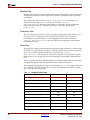
The DCM configuration, to generate a 200 MHz clock on any appropriate DCM
output (CLKFX, CLKDV, and so forth).
3.
The jitter of the derived 200 MHz reference clock, to determine if it is appropriate
for use as an input to an IDELAYCTRL.
For more information about the relevant timing parameters, see the Virtex-4 Datasheet
and User Guide. As with the other implementation options, the derived 200 MHz
reference clock must be distributed by a global clock buffer to the IDELAYCTRL
instances.
Warning: The fixed frequency requirement of the source clock precludes the use of the PCI
bus clock, unless the design is used in an embedded/closed system where the PCI bus
clock is known to be a fixed frequency. See “Bus Clock Usage” for additional information
about the allowed behavior of the PCI bus clock in compliant systems.
Regional Clock Usage
Some Virtex-4 implementations use a regional clock buffer (BUFR) for the PCI bus clock
instead of a global clock buffer (BUFG). Use of a regional clock resource greatly improves
the pin-to-pin clock to out of the interface while preserving full compliance. (Pin-to-pin
clock to out is a silicon (chip) performance parameter important for PCI.)
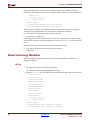
Designers must be aware of additional constraints imposed by the use of regional clocks.
Virtex-4 devices are divided into clock regions. Regional clock signals enter at the center of
a given region, and span the region of entry in addition to the region above and the region
below. The reach of a regional clock is physically limited to three clock regions. Figure 3-2
illustrates BUFR driving three clock regions. See the Virtex-4 Datasheet and User Guide for
more information about regional clocks.
32
www.xilinx.com
PCI v3.0.151 Getting Started Guide
UG157 August 31, 2005
R
Regional Clock Usage
BUFR
Figure 3-2:
Regional Clocking Illustration
For designs using regional clocking, the PCI interface and those portions of the user
application clocked from the PCI bus clock must completely fit inside the three clock
regions accessible to the regional clock signal. This restriction limits the number of FPGA
resources that may be synchronous with the PCI bus clock. Access to additional logic is
available by crossing to another clock domain.
Clock regions are 16 CLB / 32 IOB tall and one-half the width of the device. With a regional
clock span limited to three regions, this yields a maximum of 96 IOB that may be used for
a PCI interface. A 64-bit PCI interface requires 90 IOB, and a 32-bit PCI interface requires 50
IOB. In some device and package combinations (typically, physically large devices in a
relatively low pin-count packages) not all IOB sites are bonded to package pins. This
renders some clock regions unusable for PCI purposes. This is generally not an issue for 32bit PCI interfaces; however, for 64-bit PCI interfaces, it is a concern.
Table 3-4 defines all physically possible 64-bit PCI interfaces in various Virtex-4 device and
package combinations using regional clocks. Note that this does not apply to Virtex-4
designs using global clocks.
Table 3-4:
Virtex-4 Device and Package 64-bit Interfaces
Package
SF363
PCI v3.0.151 Getting Started Guide
UG157 August 31, 2005
www.xilinx.com
Device
64-bit Interfaces
LX15
none
LX25
none
FX12
none
33
R
Chapter 3: Family Specific Considerations
Table 3-4:
Virtex-4 Device and Package 64-bit Interfaces
Package
FF668
FF1148
FF1513
FF672
FF1152
FF1517
FF1760
Device
64-bit Interfaces
LX15
2
LX25
4
LX40
2
LX60
2
FX12
2
SX25
2
SX35
4
LX40
4
LX60
4
LX80
6
LX100
6
LX160
6
SX55
4
LX100
8
LX160
8
LX200
8
FX20
2
FX40
none
FX60
none
FX40
4
FX60
4
FX100
4
FX100
6
FX140
6
FX140
8
Bus Clock Usage
The bus clock output provided by the interface is derived from the bus clock input, and is
distributed using a global clock buffer. The interface itself is fully synchronous to this
clock. In general, the portion of the user application that communicates with the interface
must also be synchronous to this clock.
It is important to note that the frequency of this clock is not guaranteed to be constant. In
fact, in a compliant system, the clock may be any frequency, up to and including the
34
www.xilinx.com
PCI v3.0.151 Getting Started Guide
UG157 August 31, 2005
R
Electrical Compliance
maximum allowed frequency, and the frequency may change on a cycle-by-cycle basis.
Under certain conditions, the PCI core may also apply phase shifts to this clock.
For these reasons, the user application should not use this clock as an input to a DLL or
PLL, nor should the user application use this clock in the design of interval timers (for
example, DRAM refresh counters).
Electrical Compliance
The PCI interface targeting Virtex devices uses one of three Virtex I/O buffer types,
depending on the signaling environment (this selection is made via the wrapper file).
Note: Virtex-E, Virtex-II, Virtex-II Pro, Virtex-4, Spartan-IIE, Spartan-3, and Spartan-3E
devices are not 5.0 volt tolerant. Do not use these devices in a 5.0 volt signaling
environment.
Wrapper files for the 5.0 volt signaling environment use the PCI33_5 I/O buffers available
on Virtex and Spartan-II devices. This requires VCCO to be set at 3.3 volts, and does not
require a VREF supply. Observe the relevant specifications in the device data sheet. No
other restrictions apply.
Wrapper files for the 3.3 volt signaling environment use either the PCI33_3 or the PCI66_3
I/O buffers available on Virtex, Virtex-4, Virtex-E, Virtex-II, Virtex-II Pro, Spartan-II,
Spartan-IIE, Spartan-3, and Spartan-3E devices. With the exception of Virtex-II Pro,
Virtex-4, Spartan-3, and Spartan-3E, these require VCCO to be set at 3.3 volts, and do not
require a VREF supply. Observe the relevant specifications in the device data sheet.
For 3.3 volt signaling in Virtex-E, Virtex-II, Virtex-II Pro, Virtex-4, Spartan-IIE, Spartan-3,
and Spartan-3E devices, no other restrictions apply. However, additional restrictions do
apply for 3.3 volt signaling in Virtex and Spartan-II devices—for 3.3 volt signaling in Virtex
and Spartan-II devices, the data sheets indicate that the VIL and VIH parameters for the
input buffers are a function of VCCINT, which is a 2.5 volt supply. In the PCI Local Bus
Specification, the specifications for the 3.3 volt signaling environment state VIL and VIH as
a function of VCC. This may be considered the 3.3 volt system supply.
When the 2.5 volt and 3.3 volt supplies are at their opposite extremes, the 3.3 volt VIL or
VIH specifications will be violated. The violation is only technical, and will not affect
functionality. The VIL or VIH will not venture beyond the parameters stated in the PCI Local
Bus Specification to affect noise margins significantly. For all supply combinations, VIL will
always be within 35 mV of the specification, and VIH will be within 75 mV of the
specification. They cannot both be out of specification simultaneously.
PCI v3.0.151 Getting Started Guide
UG157 August 31, 2005
www.xilinx.com
35
R
Chapter 3: Family Specific Considerations
2.70
2.65
VCCINT (V)
2.60
2.55
3.3V PCI COMPLIANT
REGION
2.50
2.45
2.40
2.35
2.30
3.00
3.05
3.10
3.15
3.20
3.25 3.30
3.35 3.40
3.45
3.50
3.55 3.60
System Supply (V)
Figure 3-3:
Relationship For 3.3V Input Buffer Compliance
Figure 3-3 shows the small range of supply voltage values where VIL or VIH are technically
non-compliant. Note that this may occur with any PCI device if the input buffer supply
voltage is different from the supply voltage of the driving device. For best results, use a
high precision voltage regulator to generate VCCINT.
For 3.3 volt signaling in Virtex-II Pro, Virtex-4, Spartan-3, and Spartan-3E devices, the VCCO
supply must be reduced to 3.0 volts and derived from a precision regulator. This reduction
of the output driver supply provides robust device protection without sacrificing PCI
electrical compliance, even in the extreme case where the 3.3 volt system supply climbs as
high as 3.6 volts as allowed by the PCI Local Bus Specification.
36
www.xilinx.com
PCI v3.0.151 Getting Started Guide
UG157 August 31, 2005
R
Generating Bitstreams
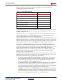
Figure 3-4 shows one possible low-cost solution to generate the required 3.0 volt output
driver supply. Xilinx recommends the use of the circuit shown in Figure 3-4, although
other approaches using other regulators are possible.
SUPPLY
8
IN
OUT
1
5
SHDN#
ADJ
2
7
GND
BYP
4
6
GND
GND
3
VCCO
38.3, 1%
LT1763CS8
+3.0V SUPPLY
1.0 uF
3.3 uF
26.1, 1%
GND
Figure 3-4:
Output Driver VCCO Generation
Virtex-II, Virtex-II Pro, Virtex-4, Spartan-3, and Spartan-3E devices, as specified in the
relevant device data sheets, exhibit a 10 pF pin capacitance. This is compliant with the PCI
Local Bus Specification, with one exception. The specification requires an 8 pF pin
capacitance for the IDSEL pin, to allow for non-resistive coupling to an AD[xx] pin. In
practice, this coupling may be resistive or non-resistive, and is performed on the system
board or backplane. For system board or backplane designs, use resistive coupling to avoid
non-compliance. For add-in cards, this is not under the control of the designer.
Although the PCI interface does not directly provide the PME# signal for power
management event reporting, it may be implemented by the user application. A typical
implementation would involve the implementation of the power management capability
item in user configuration space, along with a dedicated PME# output on a general purpose
I/O pin.
On all device families, if the FPGA power is removed, the general purpose I/O pin will
appear as a low impedance to ground. This appears to the system as an assertion of PME#.
For this reason, implementations that use the PME# signal should employ an external
buffering scheme that will prevent false assertions of PME# when power is removed from
the FPGA device.
Generating Bitstreams
The bitstream generation program, bitgen, may issue DRC warnings when generating
bitstreams for PCI designs. The number of these warnings varies depending on the
configuration options used for the PCI core. Typically, these warnings are related to nets
with no loads generated during trimming by the map program. Some of these nets are
intentionally preserved by statements in the user constraints file.
For some 66 MHz designs, bitgen must be run with a special option to change the behavior
of a global clock buffer used in the design:
bitgen -g Gclkdel<buf>:<opt> pcim_top_routed.ncd
See the release notes and the user constraints file for additional information about the use
and implications of this required option.
PCI v3.0.151 Getting Started Guide
UG157 August 31, 2005
www.xilinx.com
37
R
Chapter 3: Family Specific Considerations
This option is used to introduce additional delay on a global clock net. It is important to
note that this additional delay is observable on the CLK output of the PCI interface, which
is supplied to the user application. Timing constraints for the user application must be
generated with this in mind.
38
www.xilinx.com
PCI v3.0.151 Getting Started Guide
UG157 August 31, 2005
R
Chapter 4
Functional Simulation
This chapter describes how to simulate the ping64 example design with global clocks using
the supported functional simulation tools. For the PCI 32 interface, substitute ping32 for
ping64. If you are using a design with reference clocks, substitute with pcim_top_r and
ping_tb with ping_tb_r.
Supported functional simulation tools include
•
Cadence NC-Verilog v.5.0
•
Model Technology ModelSim v5.7b
Cadence NC-Verilog
Before attempting functional simulation, ensure that the NC-Verilog environment is
properly configured.
1.
To start, move into the functional simulation directory:
cd <Install Path>/verilog/example/func_sim
2.
Edit the ping_tb.f file. This file lists command line arguments for NC-Verilog, and is
shown below:
../source/ping_tb.v
../source/stimulus.v
../source/busrecord.v
../source/dumb_arbiter.v
../source/dumb_targ32.v
../source/dumb_targ64.v
../source/pcim_top.v
../source/ping.v
../source/cfg_ping.v
../source/glbl.v
../../src/xpci/pci_lc_i.v
../../src/xpci/pcim_lc.v
+libext+.vmd+.v
-y <Xilinx Install Path>/verilog/src/unisims
-y <Xilinx Install Path>/verilog/src/simprims
3.
Modify the library search path by changing <Xilinx Install Path> to match the
Xilinx installation directory, and then save the file.
PCI v3.0.151 Getting Started Guide
UG157 August 31, 2005
www.xilinx.com
39
R
Chapter 4: Functional Simulation
Most of the files listed are related to the example design and its testbench. For other
testbenches, the following subset must be used for proper simulation of the PCI interface:
../source/glbl.v
../../src/xpci/pci_lc_i.v
../../src/xpci/pcim_lc.v
+libext+.vmd+.v
-y <Xilinx Install Path>/verilog/src/unisims
-y <Xilinx Install Path>/verilog/src/simprims
This list does not include any configuration file, user application, top level wrapper, or
testbench. These additional files are required for a meaningful simulation.
4.
To run the NC-Verilog simulation, type the following:
ncverilog -f ping_tb.f
NC-Verilog processes the simulation files and exits. The testbench prints status messages
to the console. After the simulation completes, view the ncverilog.log file to check for
errors.
The Simvision browser may be used to view the simulation results.
5.
If desired, start Simvision with the following command:
simvision
Model Technology ModelSim
Before attempting functional simulation, ensure that the ModelSim environment is
properly configured.
Verilog
1.
Navigate to the functional simulation directory:
cd <Install Path>/verilog/example/func_sim
2.
Edit the ping_tb.f file. This file lists command line arguments, and is shown below:
../source/ping_tb.v
../source/stimulus.v
../source/busrecord.v
../source/dumb_arbiter.v
../source/dumb_targ32.v
../source/dumb_targ64.v
../source/pcim_top.v
../source/ping.v
../source/cfg_ping.v
../source/glbl.v
../../src/xpci/pci_lc_i.v
../../src/xpci/pcim_lc.v
+libext+.vmd+.v
-y <Xilinx Install Path>/verilog/src/unisims
-y <Xilinx Install Path>/verilog/src/simprims
40
www.xilinx.com
PCI v3.0.151 Getting Started Guide
UG157 August 31, 2005
R
Model Technology ModelSim
3.
Modify the library search path by changing <Xilinx Install Path> to match the
Xilinx installation directory and then save the file.
Most of the files listed are related to the example design and its testbench. For other
testbenches, the following subset must be used for proper simulation of the PCI interface:
../source/glbl.v
../../src/xpci/pci_lc_i.v
../../src/xpci/pcim_lc.v
+libext+.vmd+.v
-y <Xilinx Install Path>/verilog/src/unisims
-y <Xilinx Install Path>/verilog/src/simprims
This list does not include any configuration file, user application, top level wrapper, or
testbench. These additional files are required for a meaningful simulation.
4.
Invoke ModelSim, and ensure that the current directory is set to:
<Install Path>/verilog/example/func_sim
5.
To run the simulation:
do modelsim.do
This compiles all modules, loads them into the simulator, displays the waveform viewer,
and runs the simulation.
VHDL
1.
Navigate to the functional simulation directory:
cd <Install Path>/vhdl/example/func_sim
2.
View the ping.files file. This file lists the individual source files required, and is
shown below:
../../src/xpci/pci_lc_i.vhd
../../src/xpci/pcim_lc.vhd
../source/cfg_ping.vhd
../source/ping.vhd
../source/pcim_top.vhd
../source/busrecord.vhd
../source/dumb_arbiter.vhd
../source/dumb_targ32.vhd
../source/dumb_targ64.vhd
../source/stimulus.vhd
../source/ping_tb.vhd
Most of the files listed are related to the example design and its testbench. For other
testbenches, the following subset must be used for proper simulation of the PCI interface:
../../src/xpci/pci_lc_i.vhd
../../src/xpci/pcim_lc.vhd
This list does not include any configuration file, user application, top level wrapper, or
testbench. These additional files are required for a meaningful simulation.
3.
Invoke ModelSim, and ensure that the current directory is set to the following:
PCI v3.0.151 Getting Started Guide
UG157 August 31, 2005
www.xilinx.com
41
R
Chapter 4: Functional Simulation
<Install Path>/vhdl/example/func_sim
4.
Create the simprim and unisim libraries. This step only needs to be done once, the first
time you perform a simulation:
vlib simprim
vcom -93 -work simprim <Xilinx Install
Path>/vhdl/src/simprims/simprim_Vpackage_mti.vhd
vcom -93 -work simprim <Xilinx Install
Path>/vhdl/src/simprims/simprim_Vcomponents_mti.vhd
vcom -93 -work simprim <Xilinx Install
Path>/vhdl/src/simprims/simprim_VITAL_mti.vhd
vlib unisim
vcom -93 -work unisim <Xilinx Install
Path>/vhdl/src/unisims/unisim_VPKG.vhd
vcom -93 -work unisim <Xilinx Install
Path>/vhdl/src/unisims/unisim_VCOMP.vhd
vcom -93 -work unisim <Xilinx Install
Path>/vhdl/src/unisims/unisim_VITAL.vhd
5.
To run the simulation, enter the following:
do modelsim.do
This compiles all modules, loads them into the simulator, displays the waveform viewer,
and runs the simulation.
42
www.xilinx.com
PCI v3.0.151 Getting Started Guide
UG157 August 31, 2005
R
Chapter 5
Synthesizing a Design
This chapter describes how to synthesize the ping64 example design with global clocks
using the supported synthesis tools. For the PCI 32 interface, substitute ping32 for ping64. If
you are using a design with reference clocks, substitute pcim_top with pcim_top_r and
ping_tb with ping_tb_r.
Supported synthesis tools include
•
Synplicity Synplify v7.3
•
Exemplar LeonardoSpectrum v2003a
•
Xilinx XST
Synplicity Synplify
Before attempting to synthesize a design, ensure that the Synplicity Synplify environment
is properly configured.
Verilog
1.
Start Synplify and choose File > New, or click the new file icon on the toolbar. The New
dialog box appears.
Figure 5-5:
2.
Create a New Project
Under File Type, select Project File and enter the project name (flowtest in this example)
and synthesis directory:
<Install Path>/verilog/example/synthesis
3.
Click OK to exit the dialog box and return to the project window.
PCI v3.0.151 Getting Started Guide
UG157 August 31, 2005
www.xilinx.com
43
R
Chapter 5: Synthesizing a Design
Figure 5-6:
4.
Main Project Window
To add source files to the new project, click Add. The first file (used by any design that
instantiates Xilinx primitives) is located in:
<Synplicity Install Path>/lib/xilinx
5.
Navigate to the virtex.v file; then click Add to move this source file into the Files To
Add list.
Figure 5-7:
44
Select Files to Add (Library)
www.xilinx.com
PCI v3.0.151 Getting Started Guide
UG157 August 31, 2005
R
Synplicity Synplify
The next files are located in:
<Install Path>/verilog/src/xpci
6.
Navigate to the xpci directory, select the simulation model and the wrapper files
(pci_lc_i.v and pcim_lc.v), and click Add to move these files into the Files To Add list.
(Ctrl-click to select multiple files.)
Figure 5-8:
Files to Add (LogiCORE Files)
The final set of design files (the user application) is located in:
<Install Path>/verilog/example/source
7.
Navigate to the source directory, select the cfg_ping.v, pcim_top.v, and ping.v files,
and then click Add.
Figure 5-9: Select Files to Add Dialog Box (User Application)
PCI v3.0.151 Getting Started Guide
UG157 August 31, 2005
www.xilinx.com
45
R
Chapter 5: Synthesizing a Design
8.
After adding the three final files (for a total of six source files), click OK to return to the
main project window.
9.
In the Source Files list, view the list of newly added source files by double-clicking the
flowtest/verilog folder (if it is not already open). Reorder the source files in the
folder by dragging them to list them in the hierarchical order displayed in Figure 5-10.
Figure 5-10:
Main Project Window with Source Files
10. Click Change Result File to display the EDIF Result File dialog box; then move the to
following directory:
<Install Path>/verilog/example/synthesis
11. Name the file pcim_top.edf and click OK to set the name of the result file and return
to the main project window.
Note: In practice, the directory for the EDIF result file does not need to be changed.
However, the sample processing scripts included with the example design assume that the
output EDIF files will be located in the synthesis directory.
12. From the main project window, click Change Target to display the Options for
Implementation dialog box, as shown in Figure 5-11.
46
www.xilinx.com
PCI v3.0.151 Getting Started Guide
UG157 August 31, 2005
R
Synplicity Synplify
Figure 5-11:
Options for Implementation: Device
13. On the Device tab, set the Technology, Part, Speed, and Package options to reflect the
targeted device (a V300BG432-6 in this example). Be sure that Disable I/O Insertion is
deselected.
14. On the Options/Constraints tab, deselect Symbolic FSM Compiler (but leave Resource
Sharing selected) and set the Frequency to 66 MHz.
15. On the Implementation Results tab, deselect Write Vendor Constraint File.
16. Click OK to return to the main project window.
17. From the main project window, click Run.
Synplify synthesizes the design and writes out an optimized EDIF file. In the lowerright corner of the window, the various stages or synthesis, such as Compiling or
Mapping, are displayed. When the process is complete, Done is displayed. Note that
Synplify may issue a number of warnings (are expected) about instantiated I/O cells
and attributes used for other synthesis tools.
PCI v3.0.151 Getting Started Guide
UG157 August 31, 2005
www.xilinx.com
47
R
Chapter 5: Synthesizing a Design
VHDL
1.
Start Synplify and choose File > New, or use the new file icon on the toolbar. The New
dialog box appears.
Figure 5-12:
2.
Create a New Project
Under File Type, select Project File and enter the project name (flowtest in this example)
and synthesis directory:
<Install Path>/vhdl/example/synthesis
3.
Click OK to exit the dialog box and return to the project window.
Figure 5-13:
4.
Main Project Window
To add source files to the new project, click Add.
The first file (used by any design that instantiates Xilinx primitives) is located in:
<Synplicity Install Path>/lib/xilinx
48
www.xilinx.com
PCI v3.0.151 Getting Started Guide
UG157 August 31, 2005
R
Synplicity Synplify
5.
Select the virtex.vhd file; then click Add to move this source file into the Files To
Add list.
Figure 5-14: Select Files to Add (Library)
The next files are located in:
<Install Path>/vhdl/src/xpci
6.
Navigate to the xpci directory, select the simulation model and the wrapper files
(pci_lc_i.vhd and pcim_lc.vhd), and click Add to move these files into the Files To Add
list. (Ctrl-click to select multiple files.)
Figure 5-15:
PCI v3.0.151 Getting Started Guide
UG157 August 31, 2005
Select Files to Add (LogiCORE Files)
www.xilinx.com
49
R
Chapter 5: Synthesizing a Design
The final set of design files (the user application) is located in:
<Install Path>/vhdl/example/source
7.
Navigate to the source directory, select the cfg_ping.vhd, pcim_top.vhd, and ping.vhd,
then click Add.
8.
After adding the three final files (for a total of six source files), click OK to return to the
main project window.
9.
In the Source Files list, view the list of newly added source files by double-clicking the
flowtest/vhdl folder (if it is not already open). Drag to reorder the source files in
the hierarchical order shown in Figure 5-16.
Figure 5-16:
Project Window with Source Files
10. Click Change Result File to display the EDIF Result File dialog box; then move the to
following directory:
<Install Path>/vhdl/example/synthesis
11. Name the file pcim_top.edf and click OK to set the name of the result file and return
to the main project window.
Note: In practice, the directory for the EDIF result file does not need to be changed.
However, the sample processing scripts included with the example design assume that the
output EDIF files will be located in the synthesis directory.
50
www.xilinx.com
PCI v3.0.151 Getting Started Guide
UG157 August 31, 2005
R
Exemplar LeonardoSpectrum
12. From the main project window, click Change Target to display the Options for
Implementation dialog box, as shown in Figure 5-17.
Figure 5-17: Options for Implementation
13. On the Device tab, set the Technology, Part, Speed, and Package options to reflect the
targeted device (a V300BG432-6 in this example). Be sure that Disable I/O Insertion is
deselected.
14. On the Options/Constraints tab, deselect Symbolic FSM Compiler (leave Resource
Sharing selected) and set the Frequency to 66 MHz.
15. On the Implementation Results tab, deselect Write Vendor Constraint File.
16. Click OK to return to the main project window; then click Run.
Synplify synthesizes the design and writes out an optimized EDIF file. In the lower-right
corner of the window, the various stages or synthesis, such as Compiling or Mapping, are
displayed. When the process is complete, Done is displayed. Note that Synplify may issue
a number of warnings (which are expected) about instantiated I/O cells and attributes
used for other synthesis tools.
Exemplar LeonardoSpectrum
Before attempting to synthesize a design, ensure that the Exemplar LeonardoSpectrum
environment is properly configured for use.
1.
Navigate to the synthesis directory:
cd <Install Path>/hdl/example/synthesis
The synthesis directory contains a script for use with LeonardoSpectrum.
2.
Edit the script to change the following line:
cd <Install Path>/hdl/example/synthesis
Modify the path to point to the actual installation location, and then save the file.
3.
Invoke LeonardoSpectrum.
4.
Synthesize the design by running the script leonardo.tcl.
Note that if you run LeonardoSpectrum with the graphical user interface, the
quicksetup form cannot be used to synthesize the design. Instead, choose File > Run
Script from the menu.
PCI v3.0.151 Getting Started Guide
UG157 August 31, 2005
www.xilinx.com
51
R
Chapter 5: Synthesizing a Design
The end result of the synthesis step is an EDIF file that is fed into the Xilinx implementation
tools during the implementation step.
In practice, the provided script file must be modified to accommodate other designs. To
provide insight into the synthesis script, the major steps are presented below:
1.
Various synthesis options are set through the use of environment variables. These
must be present in the script, and should not be modified. The synthesis library is also
loaded; this may be altered for different devices and speed grades.
2.
The design is loaded by reading in the design files. At this point, the top-level module
is declared as the present_design. The script adds nopad attributes (with a value of
FALSE) to all PCI bus interface signals. The I/O structures for these ports are directly
instantiated in the wrapper file.
3.
The optimization step is done with the -hierarchy preserve and the -chip
options. The -hierarchy preserve option prevents LeonardoSpectrum from
dissolving the design hierarchy. The -chip option indicates that automatic I/O buffer
insertion should be performed.
4.
After synthesis is complete, the synthesized netlist is written.
5.
The tool may issue warnings about unused signals; these warnings are expected.
Xilinx XST
Before attempting to synthesize a design, ensure that the Xilinx XST environment is
properly configured. Synthesis is supported only from the XST command line.
1.
Navigate to the synthesis directory:
cd <Install Path>/hdl/example/synthesis
The synthesis directory contains a script for use with Xilinx XST; this script is called
run_xst.bat for PC platforms and run_xst.csh for Unix platforms. Note that the
run_xst.cmd and run_xst.prj files are common and used by both scripts.
2.
If required, modify the files as required to suit your application. You may need to
change the target architecture and select different wrapper and configuration files.
3.
Synthesize the design by running the script.
The end result of the synthesis step is an NGC file that is fed into the Xilinx
implementation tools during the implementation step. The tool may issue warnings about
unused signals; these warnings are expected.
52
www.xilinx.com
PCI v3.0.151 Getting Started Guide
UG157 August 31, 2005
R
Chapter 6
Implementing a Design
This chapter describes how to implement the ping64 example design with global clocks
using the supported FPGA implementation tools (included with the ISE Foundation v7.1
Development System). For the PCI 32 interface, substitute ping32 for ping64. If you are
using a design with reference clocks, substitute pcim_top with pcim_top_r and ping_tb with
ping_tb_r.
ISE Foundation
Before implementing a design, ensure that the Xilinx environment is properly configured
and the design has been successfully synthesized.
1.
Navigate to the implementation directory:
cd <Install Path>/hdl/example/xilinx
This directory contains the run_xilinx script that calls the appropriate tools to place and
route the example design. Scripts are provided for Unix and Microsoft Windows operating
systems.
2.
Review the appropriate run_xilinx script file, noting the following:
•
Several required special environment variables are set at the beginning of the
script; do not remove them.
•
The ngdbuild command lists both ../../src/xpci and ../synthesis as
search directories. The xpci directory contains a netlist of the PCI interface, and
the synthesis directory must contain the EDIF netlist generated during design
synthesis.
The ngdbuild command also reads a user constraints file that corresponds to a
desired target device and a particular version of the PCI interface.
•
To target a different device or to use a different version of the PCI interface, the
constraints file must be changed to match the device and interface selection. The
available selections are defined in Chapter 3, “Family Specific Considerations.”
The user constraints files provided with the PCI interface include constraints that
guarantee pinout and timing specifications. These constraints must always be
used during processing.
Additional constraints that relate to the user application must be placed in this file.
Before making additions to the user constraints file, back up the original so that it
can be restored if necessary.
•
The map command requires no special arguments, but uses an input/output
register packing option.
PCI v3.0.151 Getting Started Guide
UG157 August 31, 2005
www.xilinx.com
53
R
Chapter 6: Implementing a Design
•
The par command, as provided in the script, uses a guide file in exact guide
mode. Note that some designs do not require the use of guide files.
To target a different device or to use a different version of the PCI interface, see
Chapter 3, “Family Specific Considerations.”
If a guide file is required, ensure that the correct guide file is used by editing the
script and changing the file name. If a guide file is not required, remove the
following input arguments from the par command line in the script:
-gm exact -gf ../../src/guide/guidefile.ncd
If a guide file is required, the guide file must always be used. The effort levels and
delay cleanup iterations may be adjusted if necessary.
3.
•
The trce command performs a static timing analysis based on the design
constraints originally specified in the user constraints file.
•
The netgen command generates a simulation model of the placed and routed
design.
Implement the design by running the appropriate script.
During initial processing trials, it is useful to enter commands one at a time from the
command line rather than running the script so that you can inspect the output of each
step.
If the use of a guide file is required, it is important to verify that the guiding process was
successful. This may be done by inspecting the pcim_top_routed.grf file. The
remainder of this section is specific to designs requiring the use of guide files.
The number of pre-routed connections should exactly match the number listed in the
selection table, shown in Table 3-1, page 19. The number of unrouted signals varies
depending on the size of the user application. If the number does not match, the guide
process has failed. This can occur for several reasons. First, check that the correct user
constraints and guide files have been used. Second, verify that the user application
observes all signal-driving rules defined in the PCI User Guide.
Note: Do not attempt re-entrant routing on a guided design. Re-entrant routing must not
be used as it may re-route nets that were initially guided by the guide file.
54
www.xilinx.com
PCI v3.0.151 Getting Started Guide
UG157 August 31, 2005
R
Chapter 7
Timing Simulation
This chapter describes how to perform timing simulation using the ping64 example design
with global clocks using the supported timing simulation tools. For the PCI 32 interface,
substitute ping32 for ping64. If you are using a design with reference clocks, substitute
pcim_top with pcim_top_r and ping_tb with ping_tb_r.
Supported timing simulation tools include
•
Cadence NC-Verilog v.5.0
•
Model Technology ModelSim v5.7b
Cadence NC-Verilog
Before attempting timing simulation, ensure that the NC-Verilog environment is properly
configured for use. In addition, you must have successfully completed the implementation
phase using the Xilinx tools.
1.
Navigate to the timing simulation directory and copy the back-annotated timing
models from the implementation directory:
cd <Install Path>/verilog/example/post_sim
cp ../xilinx/pcim_top_routed.v .
cp ../xilinx/pcim_top_routed.sdf .
2.
Edit the ping_tb.f file. This file lists command line arguments for NC-Verilog, and is
shown below:
../source/ping_tb.v
../source/stimulus.v
../source/busrecord.v
../source/dumb_arbiter.v
../source/dumb_targ32.v
../source/dumb_targ64.v
../source/glbl.v
./pcim_top_routed.v
+libext+.vmd+.v
-y <Xilinx Install Path>/verilog/src/simprims
3.
Modify the library search path by changing <Xilinx Install Path> to match the
Xilinx installation directory and save the file.
4.
To run the NC-Verilog simulation:
ncverilog -f ping_tb.f
PCI v3.0.151 Getting Started Guide
UG157 August 31, 2005
www.xilinx.com
55
R
Chapter 7: Timing Simulation
NC-Verilog processes the simulation files and exits. The testbench prints status messages
to the console. After the simulation completes, view the ncverilog.log file to check for
errors.
The Simvision browser may be used to view the simulation results. Simvision is started
with the following command:
simvision
Model Technology ModelSim
Before attempting timing simulation, ensure that the ModelSim environment is properly
configured for use. In addition, you must have successfully completed the implementation
phase using the Xilinx tools.
Verilog
1.
Move into the timing simulation directory and copy the back-annotated timing models
from the implementation directory:
cd <Install Path>/verilog/example/post_sim
cp ../xilinx/pcim_top_routed.v .
cp ../xilinx/pcim_top_routed.sdf .
2.
Edit the ping_tb.f file. This file lists command line arguments, and is shown below:
../source/ping_tb.v
../source/stimulus.v
../source/busrecord.v
../source/dumb_arbiter.v
../source/dumb_targ32.v
../source/dumb_targ64.v
../source/glbl.v
./pcim_top_routed.v
+libext+.vmd+.v
-y <Xilinx Install Path>/verilog/src/simprims
3.
4.
Modify the library search path by changing <Xilinx Install Path> to match the
Xilinx installation directory. Save the file.
Invoke ModelSim, and make sure that the current directory is set to:
<Install Path>/verilog/example/post_sim
5.
Type the following to run the simulation:
do modelsim.do
This compiles all modules, loads them into the simulator, displays the waveform viewer,
and runs the simulation.
VHDL
1.
Navigate to the timing simulation directory and copy the back-annotated timing
models from the implementation directory:
cd <Install Path>/vhdl/example/post_sim
cp ../xilinx/pcim_top_routed.vhd .
56
www.xilinx.com
PCI v3.0.151 Getting Started Guide
UG157 August 31, 2005
R
Model Technology ModelSim
cp ../xilinx/pcim_top_routed.sdf .
2.
View the ping.files file. This file lists the individual source files required, and is
shown below:
./pcim_top_routed.vhd
../source/busrecord.vhd
../source/dumb_arbiter.vhd
../source/dumb_targ32.vhd
../source/dumb_targ64.vhd
../source/stimulus.vhd
../source/ping_tb.vhd
3.
Invoke ModelSim, and ensure that the current directory is set to:
<Install Path>/vhdl/example/post_sim
4.
Create the simprim library. This step is required only once, the first time you perform
a simulation:
vlib simprim
vcom -93 -work simprim <Xilinx Install
Path>/vhdl/src/simprims/simprim_Vpackage_mti.vhd
vcom -93 -work simprim <Xilinx Install
Path>/vhdl/src/simprims/simprim_Vcomponents_mti.vhd
vcom -93 -work simprim <Xilinx Install
Path>/vhdl/src/simprims/simprim_VITAL_mti.vhd
5.
Type the following to run the simulation:
do modelsim.do
This step compiles all modules, loads them into the simulator, displays the waveform
viewer, and runs the simulation.
PCI v3.0.151 Getting Started Guide
UG157 August 31, 2005
www.xilinx.com
57
R
58
Chapter 7: Timing Simulation
www.xilinx.com
PCI v3.0.151 Getting Started Guide
UG157 August 31, 2005