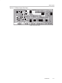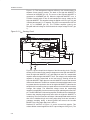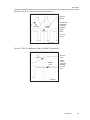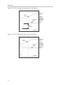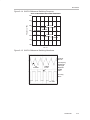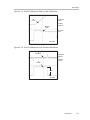
1
User’s Guide June 1999 Mixed-Signal Linear Products SLVU013 IMPORTANT NOTICE Texas Instruments and its subsidiaries (TI) reserve the right to make changes to their products or to discontinue any product or service without notice, and advise customers to obtain the latest version of relevant information to verify, before placing orders, that information being relied on is current and complete. All products are sold subject to the terms and conditions of sale supplied at the time of order acknowledgement, including those pertaining to warranty, patent infringement, and limitation of liability. TI warrants performance of its semiconductor products to the specifications applicable at the time of sale in accordance with TI’s standard warranty. Testing and other quality control techniques are utilized to the extent TI deems necessary to support this warranty. Specific testing of all parameters of each device is not necessarily performed, except those mandated by government requirements. CERTAIN APPLICATIONS USING SEMICONDUCTOR PRODUCTS MAY INVOLVE POTENTIAL RISKS OF DEATH, PERSONAL INJURY, OR SEVERE PROPERTY OR ENVIRONMENTAL DAMAGE (“CRITICAL APPLICATIONS”). TI SEMICONDUCTOR PRODUCTS ARE NOT DESIGNED, AUTHORIZED, OR WARRANTED TO BE SUITABLE FOR USE IN LIFE-SUPPORT DEVICES OR SYSTEMS OR OTHER CRITICAL APPLICATIONS. INCLUSION OF TI PRODUCTS IN SUCH APPLICATIONS IS UNDERSTOOD TO BE FULLY AT THE CUSTOMER’S RISK. In order to minimize risks associated with the customer’s applications, adequate design and operating safeguards must be provided by the customer to minimize inherent or procedural hazards. TI assumes no liability for applications assistance or customer product design. TI does not warrant or represent that any license, either express or implied, is granted under any patent right, copyright, mask work right, or other intellectual property right of TI covering or relating to any combination, machine, or process in which such semiconductor products or services might be or are used. TI’s publication of information regarding any third party’s products or services does not constitute TI’s approval, warranty or endorsement thereof. Copyright 1999, Texas Instruments Incorporated Information About Cautions and Warnings Preface Read This First About This Manual This user’s guide describes techniques for designing synchronous buck converters using TI’s SLVP1111–114 evaluation modules (EVM) and TPS56xx ripple regulator controllers. How to Use This Manual This document contains the following chapters: Chapter 1 Introduction Chapter 2 Design Procedure Chapter 3 Test Results Information About Cautions and Warnings This book may contain cautions and warnings. This is an example of a caution statement. A caution statement describes a situation that could potentially damage your software or equipment. This is an example of a warning statement. A warning statement describes a situation that could potentially cause harm to you. The information in a caution or a warning is provided for your protection. Please read each caution and warning carefully. Read This First iii Trademarks Related Documentation From Texas Instruments Synchronous Buck Converter Design Using TPS56xx Controllers in SLVP10x EVMs User’s Guide (literature number SLVU007). TPS56xx data sheet (literature number SLVS177A) Designer’s Notebook The TPS56xx Family of Power Supply Controllers (literature number SLVT140A) Designing Fast Response Synchronous Buck Regulators Using the TPS5210 (literaure number SLVA044). FCC Warning This equipment is intended for use in a laboratory test environment only. It generates, uses, and can radiate radio frequency energy and has not been tested for compliance with the limits of computing devices pursuant to subpart J of part 15 of FCC rules, which are designed to provide reasonable protection against radio frequency interference. Operation of this equipment in other environments may cause interference with radio communications, in which case the user at his own expense will be required to take whatever measures may be required to correct this interference. Trademarks TI is a trademark of Texas Instruments Incorporated. iv Running Title—Attribute Reference Contents 1 Introduction . . . . . . . . . . . . . . . . . . . . . . . . . . . . . . . . . . . . . . . . . . . . . . . . . . . . . . . . . . . . . . . . . . . . . 1-1 1.1 Synchronous Buck Regulator Operation . . . . . . . . . . . . . . . . . . . . . . . . . . . . . . . . . . . . . . . 1-2 1.2 Hysteretic Control Operation . . . . . . . . . . . . . . . . . . . . . . . . . . . . . . . . . . . . . . . . . . . . . . . . . 1-3 1.3 Design Strategy . . . . . . . . . . . . . . . . . . . . . . . . . . . . . . . . . . . . . . . . . . . . . . . . . . . . . . . . . . . . 1-4 1.4 Design Specification Summary . . . . . . . . . . . . . . . . . . . . . . . . . . . . . . . . . . . . . . . . . . . . . . . 1-5 1.5 Schematic . . . . . . . . . . . . . . . . . . . . . . . . . . . . . . . . . . . . . . . . . . . . . . . . . . . . . . . . . . . . . . . . . 1-7 1.6 Bill of Materials . . . . . . . . . . . . . . . . . . . . . . . . . . . . . . . . . . . . . . . . . . . . . . . . . . . . . . . . . . . . . 1-8 1.7 Board Layout . . . . . . . . . . . . . . . . . . . . . . . . . . . . . . . . . . . . . . . . . . . . . . . . . . . . . . . . . . . . . 1-10 2 Design Procedure . . . . . . . . . . . . . . . . . . . . . . . . . . . . . . . . . . . . . . . . . . . . . . . . . . . . . . . . . . . . . . . 2-1 2.1 TPS56xx Functions . . . . . . . . . . . . . . . . . . . . . . . . . . . . . . . . . . . . . . . . . . . . . . . . . . . . . . . . . 2-2 2.1.1 VCC Undervoltage Lockout . . . . . . . . . . . . . . . . . . . . . . . . . . . . . . . . . . . . . . . . . . . 2-3 2.1.2 Inhibit . . . . . . . . . . . . . . . . . . . . . . . . . . . . . . . . . . . . . . . . . . . . . . . . . . . . . . . . . . . . . . 2-4 2.1.3 Slowstart Design . . . . . . . . . . . . . . . . . . . . . . . . . . . . . . . . . . . . . . . . . . . . . . . . . . . . 2-4 2.1.4 Hysteresis Setting . . . . . . . . . . . . . . . . . . . . . . . . . . . . . . . . . . . . . . . . . . . . . . . . . . . 2-5 2.1.5 Noise Suppression . . . . . . . . . . . . . . . . . . . . . . . . . . . . . . . . . . . . . . . . . . . . . . . . . . 2-7 2.1.6 Overcurrent Protection . . . . . . . . . . . . . . . . . . . . . . . . . . . . . . . . . . . . . . . . . . . . . . . 2-7 2.1.7 Overvoltage Protection . . . . . . . . . . . . . . . . . . . . . . . . . . . . . . . . . . . . . . . . . . . . . . 2-10 2.1.8 Power Good . . . . . . . . . . . . . . . . . . . . . . . . . . . . . . . . . . . . . . . . . . . . . . . . . . . . . . . 2-10 2.1.9 Bias . . . . . . . . . . . . . . . . . . . . . . . . . . . . . . . . . . . . . . . . . . . . . . . . . . . . . . . . . . . . . . 2-10 2.1.10 Gate Drivers . . . . . . . . . . . . . . . . . . . . . . . . . . . . . . . . . . . . . . . . . . . . . . . . . . . . . . . 2-10 2.2 External Component Selection . . . . . . . . . . . . . . . . . . . . . . . . . . . . . . . . . . . . . . . . . . . . . . 2-14 2.2.1 Duty Cycle Estimate . . . . . . . . . . . . . . . . . . . . . . . . . . . . . . . . . . . . . . . . . . . . . . . . 2-14 2.2.2 Input Capacitance . . . . . . . . . . . . . . . . . . . . . . . . . . . . . . . . . . . . . . . . . . . . . . . . . . 2-14 2.2.3 Output Filter Design . . . . . . . . . . . . . . . . . . . . . . . . . . . . . . . . . . . . . . . . . . . . . . . . 2-14 2.2.4 Switching Frequency Analysis . . . . . . . . . . . . . . . . . . . . . . . . . . . . . . . . . . . . . . . . 2-17 2.2.5 Power MOSFET Selection . . . . . . . . . . . . . . . . . . . . . . . . . . . . . . . . . . . . . . . . . . . 2-20 3 Test Results . . . . . . . . . . . . . . . . . . . . . . . . . . . . . . . . . . . . . . . . . . . . . . . . . . . . . . . . . . . . . . . . . . . . . 3.1 Test Summary . . . . . . . . . . . . . . . . . . . . . . . . . . . . . . . . . . . . . . . . . . . . . . . . . . . . . . . . . . . . . . 3.1.1 Static Line and Load Regulation . . . . . . . . . . . . . . . . . . . . . . . . . . . . . . . . . . . . . . . 3.1.2 Output Voltage Ripple . . . . . . . . . . . . . . . . . . . . . . . . . . . . . . . . . . . . . . . . . . . . . . . . 3.1.3 Efficiency and Power Losses . . . . . . . . . . . . . . . . . . . . . . . . . . . . . . . . . . . . . . . . . . 3.1.4 Output Start-Up and Overshoot . . . . . . . . . . . . . . . . . . . . . . . . . . . . . . . . . . . . . . . 3.1.5 Frequency Variation . . . . . . . . . . . . . . . . . . . . . . . . . . . . . . . . . . . . . . . . . . . . . . . . . 3.1.6 Load Current Transient Response . . . . . . . . . . . . . . . . . . . . . . . . . . . . . . . . . . . . . 3.1.7 Features . . . . . . . . . . . . . . . . . . . . . . . . . . . . . . . . . . . . . . . . . . . . . . . . . . . . . . . . . . . 3.1.8 Conclusion . . . . . . . . . . . . . . . . . . . . . . . . . . . . . . . . . . . . . . . . . . . . . . . . . . . . . . . . . 3.2 Test Setup . . . . . . . . . . . . . . . . . . . . . . . . . . . . . . . . . . . . . . . . . . . . . . . . . . . . . . . . . . . . . . . . . 3.3 Test Results . . . . . . . . . . . . . . . . . . . . . . . . . . . . . . . . . . . . . . . . . . . . . . . . . . . . . . . . . . . . . . . . Chapter Title—Attribute Reference 3-1 3-2 3-2 3-2 3-2 3-2 3-3 3-3 3-3 3-4 3-5 3-7 v Running Title—Attribute Reference Figures 1–1 1–2 1–3 1–4 1–5 1–6 1–7 2–1 2–2 2–3 2–4 2–5 2–6 3–1 3–2 3–3 3–4 3–5 3–6 3–7 3–8 3–9 3–10 3–11 3–12 3–13 3–14 3–15 3–16 3–17 3–18 3–19 3–20 3–21 3–22 3–23 3–24 3–25 3–26 vi Simplified Synchronous Buck Converter Schematic . . . . . . . . . . . . . . . . . . . . . . . . . . . . . . . . 1-2 Simplified Hysteretic Controlled Output Voltage Waveform . . . . . . . . . . . . . . . . . . . . . . . . . . 1-3 SLVP111–114 EVM Converter Schematic Diagram . . . . . . . . . . . . . . . . . . . . . . . . . . . . . . . . 1-7 Top Assembly . . . . . . . . . . . . . . . . . . . . . . . . . . . . . . . . . . . . . . . . . . . . . . . . . . . . . . . . . . . . . . . 1-10 Bottom Assembly (Top View) . . . . . . . . . . . . . . . . . . . . . . . . . . . . . . . . . . . . . . . . . . . . . . . . . . 1-10 Top Layer . . . . . . . . . . . . . . . . . . . . . . . . . . . . . . . . . . . . . . . . . . . . . . . . . . . . . . . . . . . . . . . . . . . 1-10 Bottom Layer (Top VIew) . . . . . . . . . . . . . . . . . . . . . . . . . . . . . . . . . . . . . . . . . . . . . . . . . . . . . . 1-11 TPS56xx Functional Block Diagram . . . . . . . . . . . . . . . . . . . . . . . . . . . . . . . . . . . . . . . . . . . . . 2-3 Block Diagram Showing Noise Suppression Circuits . . . . . . . . . . . . . . . . . . . . . . . . . . . . . . . 2-7 VDS Sensing Circuit . . . . . . . . . . . . . . . . . . . . . . . . . . . . . . . . . . . . . . . . . . . . . . . . . . . . . . . . . . . 2-8 Gate Driver Block Diagram . . . . . . . . . . . . . . . . . . . . . . . . . . . . . . . . . . . . . . . . . . . . . . . . . . . . 2-11 I–V Characteristic Curve for Low-Side Gate Drivers . . . . . . . . . . . . . . . . . . . . . . . . . . . . . . . 2-12 Output Ripple Voltage Detail . . . . . . . . . . . . . . . . . . . . . . . . . . . . . . . . . . . . . . . . . . . . . . . . . . . 2-18 Test Setup . . . . . . . . . . . . . . . . . . . . . . . . . . . . . . . . . . . . . . . . . . . . . . . . . . . . . . . . . . . . . . . . . . . 3-6 SLVP111 Measured Load Regulation . . . . . . . . . . . . . . . . . . . . . . . . . . . . . . . . . . . . . . . . . . . . 3-7 SLVP111Measured Efficiency . . . . . . . . . . . . . . . . . . . . . . . . . . . . . . . . . . . . . . . . . . . . . . . . . . . 3-7 SLVP111Measured Power Dissipation . . . . . . . . . . . . . . . . . . . . . . . . . . . . . . . . . . . . . . . . . . . 3-8 SLVP111Measured Switching Frequency . . . . . . . . . . . . . . . . . . . . . . . . . . . . . . . . . . . . . . . . . 3-8 SLVP111 Measured Switching Waveforms . . . . . . . . . . . . . . . . . . . . . . . . . . . . . . . . . . . . . . . . 3-9 SLVP111Measured Start-Up (INHIBIT) Waveforms . . . . . . . . . . . . . . . . . . . . . . . . . . . . . . . . 3-9 SLVP111 Measured Start-Up (VCC) Waveforms . . . . . . . . . . . . . . . . . . . . . . . . . . . . . . . . . . 3-10 SLVP111Measured Start-Up (VIN) Waveforms . . . . . . . . . . . . . . . . . . . . . . . . . . . . . . . . . . . 3-10 SLVP111 Measured Load Transient Waveforms . . . . . . . . . . . . . . . . . . . . . . . . . . . . . . . . . . 3-11 SLVP112 Measured Load Regulation . . . . . . . . . . . . . . . . . . . . . . . . . . . . . . . . . . . . . . . . . . . 3-11 SLVP112 Measured Efficiency . . . . . . . . . . . . . . . . . . . . . . . . . . . . . . . . . . . . . . . . . . . . . . . . . 3-12 SLVP112 Measured Power Dissipation . . . . . . . . . . . . . . . . . . . . . . . . . . . . . . . . . . . . . . . . . . 3-12 SLVP112 Measured Switching Frequency . . . . . . . . . . . . . . . . . . . . . . . . . . . . . . . . . . . . . . . 3-13 SLVP112 Measured Switching Waveforms . . . . . . . . . . . . . . . . . . . . . . . . . . . . . . . . . . . . . . 3-13 SLVP112 Measured Start-Up (INHIBIT) Waveforms . . . . . . . . . . . . . . . . . . . . . . . . . . . . . . . 3-14 SLVP112 Measured Start-Up (VCC) Waveforms . . . . . . . . . . . . . . . . . . . . . . . . . . . . . . . . . . 3-14 SLVP112 Measured Start-Up (VIN) Waveforms . . . . . . . . . . . . . . . . . . . . . . . . . . . . . . . . . . . 3-15 SLVP112 Measured Load Transient Waveforms . . . . . . . . . . . . . . . . . . . . . . . . . . . . . . . . . . 3-15 SLVP113 Measured Load Regulation . . . . . . . . . . . . . . . . . . . . . . . . . . . . . . . . . . . . . . . . . . . 3-16 SLVP113 Measured Efficiency . . . . . . . . . . . . . . . . . . . . . . . . . . . . . . . . . . . . . . . . . . . . . . . . . 3-16 SLVP113 Measured Power Dissipation . . . . . . . . . . . . . . . . . . . . . . . . . . . . . . . . . . . . . . . . . . 3-17 SLVP113 Measured Switching Frequency . . . . . . . . . . . . . . . . . . . . . . . . . . . . . . . . . . . . . . . 3-17 SLVP113 Measured Switching Waveforms . . . . . . . . . . . . . . . . . . . . . . . . . . . . . . . . . . . . . . 3-18 SLVP113 Measured Start-Up (INHIBIT) Waveforms . . . . . . . . . . . . . . . . . . . . . . . . . . . . . . . 3-18 SLVP113 Measured Start-Up (VCC) Waveforms . . . . . . . . . . . . . . . . . . . . . . . . . . . . . . . . . . 3-19 Running Title—Attribute Reference 3–27 3–28 3–29 3–30 3–31 3–32 3–33 3–34 3–35 3–36 3–37 SLVP113 Measured Start-Up (VIN) Waveforms . . . . . . . . . . . . . . . . . . . . . . . . . . . . . . . . . . . SLVP113 Measured Load Transient Waveforms . . . . . . . . . . . . . . . . . . . . . . . . . . . . . . . . . . SLVP114 Measured Load Regulation . . . . . . . . . . . . . . . . . . . . . . . . . . . . . . . . . . . . . . . . . . . SLVP114 Measured Efficiency . . . . . . . . . . . . . . . . . . . . . . . . . . . . . . . . . . . . . . . . . . . . . . . . . SLVP114 Measured Power Dissipation . . . . . . . . . . . . . . . . . . . . . . . . . . . . . . . . . . . . . . . . . . SLVP114 Measured Switching Frequency . . . . . . . . . . . . . . . . . . . . . . . . . . . . . . . . . . . . . . . SLVP114 Measured Switching Waveforms . . . . . . . . . . . . . . . . . . . . . . . . . . . . . . . . . . . . . . SLVP114 Measured Start-Up (INHIBIT) Waveforms . . . . . . . . . . . . . . . . . . . . . . . . . . . . . . . SLVP114 Measured Start-Up (VCC) Waveforms . . . . . . . . . . . . . . . . . . . . . . . . . . . . . . . . . . SLVP114 Measured Start-Up (VIN) Waveforms . . . . . . . . . . . . . . . . . . . . . . . . . . . . . . . . . . . SLVP114 Measured Load Transient Waveforms . . . . . . . . . . . . . . . . . . . . . . . . . . . . . . . . . . 3-19 3-20 3-20 3-21 3-21 3-22 3-22 3-23 3-23 3-24 3-24 Tables 1–1 1–2 1–3 Summary of EVM Converter Modules . . . . . . . . . . . . . . . . . . . . . . . . . . . . . . . . . . . . . . . . . . . . 1-4 EVM Converter Operating Specifications . . . . . . . . . . . . . . . . . . . . . . . . . . . . . . . . . . . . . . . . . 1-5 SLVP111–114 EVMs Bill of Materials . . . . . . . . . . . . . . . . . . . . . . . . . . . . . . . . . . . . . . . . . . . . 1-8 Contents vii viii Chapter 1 Introduction The SLVP111/112/113/114 evaluation modules (EVMs) have been designed and tested using the TPS56xx hysteretic controllers. These boards are synchronous dc-dc buck converters with fixed output voltages of 3.3 V, 2.5 V, 1.8 V and 1.5 V respectively. They use only surface mount components and are design examples of how to use TI’s TPS56xx controllers in high density, low loss applications with tight static and dynamic output voltage requirements. Detailed test results taken from the EVMs are presented. Design simplicity, low component count, and lower cost make buck converters popular solutions where low input voltages are available for the converter and where isolation is not a requirement. This user’s guide describes techniques for designing synchronous buck converters using TI’s SLVP111–114 EVMs and TPS56xx ripple regulator controllers. Synchronous buck converters provide an elegant power supply solution for rapidly transitioning DSP loads (such as the Texas Instruments TMS320C62x/67x family), fast memory, and similar processors. An order of magnitude improvement in dynamic response of this converter over standard control methods reduces hold-up capacitance needs near the transitioning loads, thus saving cost and board space. Topic Page 1.1 Synchronous Buck Regulator Operation . . . . . . . . . . . . . . . . . . . . . . . . 1–2 1.2 Hysteretic Control Operation . . . . . . . . . . . . . . . . . . . . . . . . . . . . . . . . . . . 1–3 1.3 Design Strategy . . . . . . . . . . . . . . . . . . . . . . . . . . . . . . . . . . . . . . . . . . . . . . . 1–4 1.4 Design Specification Summary . . . . . . . . . . . . . . . . . . . . . . . . . . . . . . . . . 1–5 1.5 Schematic . . . . . . . . . . . . . . . . . . . . . . . . . . . . . . . . . . . . . . . . . . . . . . . . . . . . 1–7 1.6 Bill of Materials . . . . . . . . . . . . . . . . . . . . . . . . . . . . . . . . . . . . . . . . . . . . . . . 1–8 1.7 Board Layout . . . . . . . . . . . . . . . . . . . . . . . . . . . . . . . . . . . . . . . . . . . . . . . 1–10 Introduction 1-1 Synchronous Buck Regulator Operation 1.1 Synchronous Buck Regulator Operation The synchronous buck converter is a variation of the traditional buck converter. The main switching device is usually a power MOSFET and is driven in the same manner as in a traditional buck converter. The freewheeling rectifier, usually a Schottky device, is replaced by a power MOSFET and is driven in a complementary or synchronous fashion relative to the main switching device; when one MOSFET is on, the other is off. The freewheeling MOSFET is selected so that its ON voltage drop is less than the forward drop of the original freewheeling rectifier, thus increasing conversion efficiency. A very important design issue when using a synchronous buck converter is preventing cross-conduction of the two power MOSFETs, i.e., preventing both MOSFETs from being on simultaneously. A small amount of deadtime is necessary. Figure 1 shows a simplified schematic of a synchronous buck converter. The TPS56xx senses the output voltage and then drives Q1 and Q2 depending on the sensed voltage. The TPS56xx senses the voltage at the junction of Q1, Q2, and L1 and uses it to actively prevent simultaneous conduction of Q1 and Q2. Figure 1–1. Simplified Synchronous Buck Converter Schematic VI Q1 + L1 TPS56xx VO Q2 + C 1-2 Hysteretic Control Operation 1.2 Hysteretic Control Operation Hysteretic control, also called bang-bang control or ripple regulator control, maintains the output voltage within the hysteresis band centered about the internal reference voltage. Figure 1–2 shows a simplified example of a hysteretic controlled output voltage using the TPS5625 with a reference voltage of 2.500 V and a hysteresis band of 50 mV. If the output voltage is at or below the level of the reference minus one-half of the hysteresis band (VLo = 2.475 V), the TPS5625 turns off the low-side MOSFET (Q2 in Figure 1–1) and turns on the high-side MOSFET (Q1 in Figure 1–1) of the synchronous buck converter power stage. This is the power stage on-state, and it causes the output voltage to increase. When the output voltage reaches or exceeds the reference plus one-half of the hysteresis band (VHi = 2.525 V), the TPS5625 turns off the high-side MOSFET and turns on the low-side MOSFET. This is the power stage off-state, and it causes the output voltage to decrease. This hysteretic method of control keeps the output voltage within the hysteresis band around the reference voltage. If output-load current steps or input-voltage transients force the output voltage out of the hysteresis band, the TPS5625 sets the power-stage MOSFETs in the continuous on or off state as required to return the output voltage to the hysteresis band. Thus, the output voltage is corrected as quickly as the output filter allows. There are no error amplifier sensing and adjusting delays, as is the case with either voltageor current-mode controllers. Other advantages of hysteretic control include no loop compensation design and no input filter interaction problems. Figure 1–2. Simplified Hysteretic Controlled Output Voltage Waveform Output Voltage VHi 2.525 V Hysteresis 2.500 V 2.475 V VLo Time On Time Off Time Ts Introduction 1-3 Design Strategy 1.3 Design Strategy The SLVP111–114 evaluation modules (EVMs) are optimized for 5-V main input voltage and 6-A output current. The EVMs need an additional low current 12-V (30 mA max) input voltage for the controller. TI’s application report, Providing a DSP Power Solution from 5 V or 3.3 V Only Systems, TI literature number SPRA525 describes how one can implement a simple boost circuit for 5-V only input voltage applications. These EVMs are pin to pin compatible with SLVP104/105/106/115 evaluation boards with 8 A output current, which combine surface mount and through hole components. This surface mount version has the same length, 2″, and width, 0.75″, but the height is significantly lower, 0.375″ versus 0.6″ for through hole version. The TI SLVP111–114 evaluation modules (EVM) provide synchronous buck converter circuits for evaluating the capabilities of the TPS56xx family of ripple regulator controllers. The EVM converters can provide proven, demonstrated reference designs to aid in the rapid development of application-specific synchronous buck converters. Output capacities of the EVM converters are optimized for the Siliconix Si4410 power MOSFET device. The 6-ampere output current level is a reasonable selection criteria for powering circuit cards with multiple DSPs, and for providing the regulated voltage to other hardware on the circuit card. Component size can be reduced for designs requiring lower power levels. The TPS56xx controllers each provide one of four popular output voltage levels. The last two digits of the part number correlate to the set-point voltage level: TPS5633 is the 3.3-V controller, TPS5625 is the 2.5-V controller, TPS5618 is the 1.8-V controller, and TPS5615 is the 1.5-V controller. Many digital devices, memories, and DSP I/O circuits use the 3.3-V level. The core of the TMS320C6201 requires 2.5-V. All of the other DSPs in the TMS320C62x and the TMS320C67x family need 1.8 V. The GTL bus, as well as various processors and future DSPs, may require the 1.5-V controller. An external resistor divider can be used to fine tune the output voltages of these controllers for other applications including output voltages up to approximately VIN – 0.5 V. Table 1–1 summarizes the four EVM converter modules. Table 1–1. Summary of EVM Converter Modules EVM Part Number EVM Board Number Controller Output Voltage Max. Output Current TPS5633EVM–111 SLVP111 TPS5633 3.3 V 6 A† TPS5625EVM–112 SLVP112 TPS5625 2.5 V 6 A† TPS5618EVM–113 SLVP113 TPS5618 1.8 V 6 A† TPS5615EVM–114 SLVP114 TPS5615 1.5 V 6 A† † Output current is limited by the temperature rise of the power MOSFETs chosen. Higher or lower current designs are possible. 1-4 Design Specification Summary 1.4 Design Specification Summary This section summarizes the design requirements of the EVM converters. Although every attempt was made to accurately describe the performance of the EVM converters and the TPS56xx controllers, in case of conflicts, the TPS56xx data sheet takes precedence over this document. The TPS56xx family of controllers provides the necessary regulation functions. In addition to a reference voltage accuracy of ±1% over the full operating temperature range, the controller has remote sense inputs to provide a precisely regulated output voltage. The controller also provides undervoltage lock-out, overload protection, overvoltage protection, and overtemperature protection. The controller has a logic level INHIBIT input to control the converter turn-on and turn-off and a power good output to indicate output voltage status. Undervoltage lock-out prevents operation of the power supply when the 12 Vdc input voltage is not sufficient for proper operation. Overload protection protects the power supply from accidental overloads or short circuits. Overvoltage protection prevents damage to the load in the event of an internal power supply failure or presence of high voltages on the output from an external condition. Both overvoltage and overcurrent cause a latched shutdown. Both power MOSFETs are driven to an OFF state. Recovery from shutdown requires removal of the 12 V control input supply for reset. Table 1–2 lists the operating specifications of the EVM converters. Table 1–2. EVM Converter Operating Specifications Specification Min Typ Max Units Power input voltage range 4.5 6 V Control input voltage range 10.8 13.2 V Static voltage tolerance† SLVP111 (3.3 V) SLVP112 (2.5 V) SLVP113 (1.8 V) SLVP114 (1.5 V) 3.27 2.47 1.78 1.48 3.30 2.50 1.80 1.50 3.33 2.53 1.82 1.52 V V V Line regulation‡ ± 0.05% ± 0.1% Load regulation§ ± 0.2% ± 0.4% ± 100 50 Transient response¶ Output current range# 0 Current limit# O erating frequencyk Operating SLVP111 ((3.3 V)) SLVP112 (2.5 V) SLVP113 (1.8 V) SLVP114 (1 (1.8 8 V) 135 225 295 360 mV pk µsec 6 A 10 A kHz kHz kHz kH kHz Introduction 1-5 Design Specification Summary Table 1–2. EVM Converter Operating Specifications (Continued) Specification Min Typ Output ripple|| SLVP111 (3.3 V) SLVP112 (2.5 V) SLVP113 (1.8 V) SLVP114 (1.5 V) 66 50 36 30 Efficiency, 6 A load SLVP111 (3.3 V) SLVP112 (2.5 V) SLVP113 (1.8 V) SLVP114 (1.5 V) 90% 86.4% 83.2% 79.8% Efficiency, 4 A load SLVP111 (3.3 V) SLVP112 (2.5 V) SLVP113 (1.8 V) SLVP114 (1.5 V) 91.6% 88.6% 85.1% 81.9% Max Units mV p–p mV p–p mV p–p mV p–p † Vi = 5 V, Io = 6 A ‡ Io = 6 A, Vi = 5 V ±10% § Vi = 5 V ¶ Vi = 5 V, Io stepped repetitively from 0 A to 6.5 A # Output current rating is limited by thermal considerations. Load currents above this rating may cause damage to the power supply. || Unless otherwise specified, all test conditions are TA = 25_C, Vi = 5 V, Io = 6 A, Vo = nominal. k Vi = 5 V, Io = 6 A, Vo = nominal 1-6 J1–7 12 V RETURN J1–8 PG J1–3 J1–1 INHIBIT RETURN J1–10 J1–9 J1–6 C19 0.01 µ F C17 0.1 µ F R1 1 kΩ R2 10 kΩ R10 20 kΩ 1% R10 100 Ω 1% C20 1000 pF R11 20 kΩ 1% NOTE: Last two digits of U1 indicates output voltage option TPS5633 = 3.3 V (SLVP111) TPS5625 = 2.5 V (SLVP112) TPS5618 = 1.8 V (SLVP113) TPS5618 = 1.5 V (SLVP114) R13 750 Ω 11 kΩ R9 R7 1 kΩ 33 µ F 10 V C1 + U1 TPS5633 (See Note) J1–5 C6 0.1 µ F C5 C7 C21 0.1 µ F 1µF C16 C8 R3 10 Ω R4 L1 Q1 Si4410 C18 0.1 µ F Q2 Si4410 2.2 µ H 10 Ω 100 Ω 1% R8 R15 1M 1µF C22 1µF 0.1 µ F 1µF 28 PWRGD IOUT 27 AGND2 NC 26 OCP NC 25 VHYST NC 24 VREFB NC 23 VSENSE NC 22 ANAGND INHIBIT 21 SLOWST IOUTLO 20 BIAS LOSENSE 19 HISENSE LODRV 18 BOOTLO LOHIB 17 DRVGND HUGHDR 16 BOOT LOWDR 15 VCC DRV 1 2 3 4 5 6 7 8 9 10 11 12 13 14 C2 C3 + C4 + 6.3 V 150 µ F 6.3 V 150 µ F 6.3 V 150 µ F R12 4.7 Ω 2.2 µ F C9 + VI C10 150 µ F 4V C15 0.01 µ F R5 2.7 Ω 1.5 µ H L2 + C11 150 µ F + C12 150 µ F + C13 150 µ F + C14 10 µ F R6 4.7 Ω SLVP111 = 3.3 V SLVP112 = 2.5 V SLVP113 = 1.8 V SLVP114 = 1.5 V J1–14 J1–13 J1–12 J1–11 J1–2 J1–4 J1–18 J1–17 J1–16 J1–15 PWR GND V SENSEL/ ANAGND V SENSEH VO Schematic 1.5 Schematic Figure 1–3 shows the EVM converter schematic diagram. The schematic diagrams for the other EVM converters are identical except for the controller IC used. Figure 1–3. SLVP111–114 EVM Converter Schematic Diagram Introduction 1-7 Bill of Materials 1.6 Bill of Materials Table 1–3 lists materials required for the SLVP111–114 EVMs. Table 1–3. SLVP111–114 EVMs Bill of Materials Ref Des Part Number Description MFG C1 10TPA33M Capacitor, POSCAP, 33 µF, 10 V, 20% Sanyo C2 6TPB150M Capacitor, POSCAP, 150 µF, 6.3 V, 20% Sanyo C3 6TPB150M Capacitor, POSCAP, 150 µF, 6.3 V, 20% Sanyo C4 6TPB150M Capacitor, POSCAP, 150 µF, 6.3 V, 20% Sanyo C5 GRM39X7R104K016A Capacitor, Ceramic, 0.1 µF, 16 V, 10%, X7R muRata C6 GRM39X7R104K016A Capacitor, Ceramic, 0.1 µF, 16 V, 10%, X7R muRata C7 GRM42–6Y5V105Z016A Capacitor, Ceramic, 1.0 µF, 16 V, +80%–20% muRata C8 GRM42–6Y5V105Z016A Capacitor, Ceramic, 1.0 µF, 16V, +80%–20% muRata C9 GRM42–6Y5V225Z016A Capacitor, Ceramic, 2.2 µF, 16V, Y5V muRata C10 4TPC150M Capacitor, POSCAP, 150 µF, 4 V, 20% Sanyo C11 4TPC150M Capacitor, POSCAP, 150 µF, 4 V, 20% Sanyo C12 4TPC150M Capacitor, POSCAP, 150 µF, 4 V, 20% Sanyo C13 4TPC150M Capacitor, POSCAP, 150 µF, 4 V, 20% Sanyo C14 GRM235Y5V106Z016A Capacitor, Ceramic, 10 µF, 16 V, Y5V muRata C15 GRM42-6Y5V103Z025A Capacitor, Ceramic, 0.01 µF, 25 V, +80%–20%, Y5V muRata C16 GRM42–6Y5V105Z016A Capacitor, Ceramic, 1.0 µF, 16 V, +80%–20% muRata C17 GRM39X7R104K016A Capacitor, Ceramic, 0.1 µF, 16 V, 10%, X7R muRata C18 GRM39X7R104K016A Capacitor, Ceramic, 0.1 µF, 16 V, 10%, X7R muRata C19 GRM39X7R103K025A Capacitor, Ceramic, 0.01 µF, 25 V, 10%, X7R muRata C20 GRM39X7R102K050A Capacitor, Ceramic, 1000 pF, 50 V, 10%, X7R muRata C21 GRM39X7R104K016A Capacitor, Ceramic, 0.1 µF, 16 V, 10%, X7R muRata C22 GRM42–6Y5V105Z016A Capacitor, Ceramic, 1.0 µF, 16 V, +80%–20% muRata J1 S1122–18–ND Header, RA, 18-pin, 0.23 Posts x 0.20 Tails Sullins L1 DO3316P–222HC Inductor, 2.2 µH, 7.4 A Coilcraft L2 DO3316P–152HC Inductor, 1.5 µH, 9 A Coilcraft Q1 Si4410DY FET, N-ch, 30-V, 10-A, 13-mΩ Siliconix Q2 Si4410DY FET, N-ch, 30-V, 10-A, 13-mΩ Siliconix R1 Std Resistor, Chip, 1 kΩ, 1/16W, 5% R2 Std Resistor, Chip, 10 kΩ, 1/16W, 5% R3 Std Resistor, Chip, 10 Ω, 1/10W, 5% R4 Std Resistor, Chip, 10 Ω, 1/10W, 5% R5 Std Resistor, Chip, 2.7 Ω, 1/4W, 5% R6 Std Resistor, Chip, 4.7 Ω, 1/16W, 5% 1-8 Bill of Materials Table 1–3. SLVP111–114 EVMs Bill of Materials (Continued) Ref Des Part Number Description MFG R7 Std Resistor, Chip, 1 kΩ, 1/16W, 5% R8 Std Resistor, Chip, 100 Ω, 1/16W, 1% R9 Std Resistor, Chip, 11 kΩ, 1/16W, 5% R10 Std Resistor, Chip, 100 Ω, 1/16W, 1% R11 Std Resistor, Chip, 20 kΩ, 1/16W, 1% R12 Std Resistor, Chip, 4.7 Ω, 1/16W, 5% R13 Std Resistor, Chip, 750 Ω, 1/16W, 5% R14 Std Resistor, Chip, 20 kΩ, 1/16W, 1% R15 Std Resistor, Chip, 1 MΩ, 1/16W, 5% U1a TPS5633PWP IC, PWM Ripple Controller, Fixed 3.3-V (SLVP111 only) TI U1b TPS5625PWP IC, PWM Ripple Controller, Fixed 2.5-V (SLVP112 only) TI U1c TPS5618PWP IC, PWM Ripple Controller, Fixed 1.8-V (SLVP113 only) TI U1d TPS5615PWP IC, PWM Ripple Controller, Fixed 1.5-V (SLVP114 only) TI Introduction 1-9 Board Layout 1.7 Board Layout Figures 1–4 through 1–7 show the board layouts for the SLVP111–114 evaluation modules. Figure 1–4. Top Assembly Top Assembly Figure 1–5. Bottom Assembly (Top View) Bottom Assembly (Top View) Figure 1–6. Top Layer Top Layer 1-10 Board Layout Figure 1–7. Bottom Layer (Top VIew) Bottom Layer (Top View) Introduction 1-11 1-12 Chapter 2 Design Procedure The SLVP111–114 are dc-dc synchronous buck converter evaluation modules (EVMs) that provide a regulated output voltage at up to 6 A with a power input voltage range of 4.5 V to 6 V. A low power 12-V, 20-mA source is also required to power the TPS56xx controller. The controller operates at a nominal frequency of 135 kHz for 5 V input and 3.3 V output. To provide the highest level of performance, the EVM converters use hysteretic, or ripple, control. Hysteretic-controlled synchronous buck converters have several advantages over conventional PWM-controlled power supplies: Correction of output voltage variations caused by output-load or input- voltage transients is extremely fast. The user controls output ripple by adjusting the operational parameters of the converter, instead of relying on brute force methods requiring the choice of an output filter. Hysteretic control sets the operational frequency of the converter. For a given set of external components, the lower the permissible ripple setting, the higher the operational frequency. There is no control loop to design. Topic Page 2.1 TPS56xx Functions . . . . . . . . . . . . . . . . . . . . . . . . . . . . . . . . . . . . . . . . . . . 2–2 2.2 External Component Selection . . . . . . . . . . . . . . . . . . . . . . . . . . . . . . . 2–14 Design Procedure 2-1 TPS56xx Functions 2.1 TPS56xx Functions The functional block diagram of the TPS56xx family of controllers is given in Figure 2–1. The controller has the following main features: ±1% reference over 0°C to125°C junction temperature range. Synchronous-buck gate drivers with adaptive deadtime control High-side MOSFET driver voltage rating of 30 V MOSFET driver peak current rating of 2 A Hysteretic comparator: 250-ns propagation delay to gate driver outputs, 2.5-mV offset voltage, symmetrical hysteresis, hysteresis setting is a percentage of Vref. Lossless output current sensing circuit Slowstart circuit; slowstart time independent of VID setting Internal 8-V drive regulator for reduced gate charge power losses POWERGOOD comparator, 93% of Vref trip UVLO, Vcc undervoltage lockout, 10-V start, 2-V hysteresis INHIBIT comparator that can also monitor UVLO of the system logic supply, 2.1-V start, 100-mV hysteresis. Latched overcurrent shutdown circuit Latched overvoltage shutdown circuit LODRV pin that activates the low-side MOSFETs as a crowbar to protect against a short across the high-side MOSFETs. 2-2 TPS56xx Functions Figure 2–1. TPS56xx Functional Block Diagram 15 VCC 7 ANAGND 28 20 PWRGD LOSENSE 19 21 IOUTLO HISENSE VCC 2V + _ 22 INHIBIT UVLO 10 V 3 OCP _ 1 IOUT Shutdown S VCC 2X Q Fault Deglitch + Rising Edge Delay R HIGHDR 100mV HIGHIN Deglitch VPGD 0.93 VREF VOVP 1.15 VREF VCC VSENSE Analog Bias IVREFB 5 8 SLOWST Analog Bias PREREG Slowstart Comparator + _ 9 BIAS 14 DRV DRV REG Shutdown 16 BOOT 17 HIGHDR _ Bandgap Shutdown CM Filters + VREF + _ + _ 18 BOOTLO Hysteresis Comparator 13 LOWDR 12 DRVGND Hysteresis Setting I VREFB 2 AGND2 5 VREFB 4 VHYST 6 VSENSE 11 LOHIB 10 LODRV This section describes the functions governed by the TPS556xx. A procedure is given to determine the values of components used in the example design given in Figure 1–3. Example calculations for the 3.3-V output version accompany the design equations. There are many possible ways to proceed when designing power supplies and some iteration may be necessary when actual performance differs from design predictions. Reference designators refer to the circuit in Figure 1–3. 2.1.1 VCC Undervoltage Lockout The VCC undervoltage lockout circuit disables the controller while VCC is below the 10-V start threshold during power up. While the controller is disabled, the output drivers will be low and the slowstart capacitor will be shorted. When VCC exceeds the start threshold, the short across the slowstart capacitor is released and normal converter operation begins. There is a 2-V hysteresis in the undervoltage lockout circuit for noise immunity. Design Procedure 2-3 TPS56xx Functions 2.1.2 Inhibit The inhibit circuit is a comparator with a 2.1-V start voltage and a 100-mV hysteresis. When inhibit is low, the output drivers are low and the slowstart capacitor is discharged. When inhibit is above the start threshold, the short across the slowstart capacitor is released and normal operation begins. When the system logic supply is connected to the inhibit pin, the inhibit pin also controls power sequencing by locking out controller operation until the system logic supply exceeds the input threshold voltage of the inhibit circuit; thus, the 12-V supply and the system logic supply must be above UVLO thresholds before the controller is allowed to start up. 2.1.3 Slowstart Design Slowstart or soft-start is added to reduce power-up transients. Without slowstart, when input power is first applied, the TPS56xx attempts to raise the output voltage (initially zero) to its normal operating level by turning on the top MOSFET until the voltage is approximately Vref. This can cause high transient currents to flow in the output inductor and output capacitor. Although this form of startup usually does not cause component failures, it does apply stresses much greater than those typically encountered in normal operation. It is good design practice to include slowstart circuitry to avoid these unnecessary stresses. The slowstart circuit in the TPS56xx controls the rate at which the output voltage powers up. A capacitor, C21, connected between SLOWST (pin 8) and ANAGND (pin 7), is charged by an internal current source. This current source is proportional to the reference voltage and is adjustable by an external resistance selected by the user. The output voltage follows the voltage on the slowstart capacitor during startup. Since the charging current is proportional to the reference voltage, the slowstart time is independent of the reference voltage for a given resistor value. Choices of the slowstart time and the slowstart capacitor value are largely arbitrary as long as system start-up time requirements are met. For this example design, a slowstart time of 10 ms is chosen, and the slowstart capacitor is chosen to be 0.1 µF. Therefore, to charge 0.1 µF from zero volts to 3.3 V in 10 ms, the following equation holds: V c I SLOWSTART C SLOWSTART 0.1 F 3.3 V 33 A t ss 10 ms The slowstart charging current is determined by the following equation: I SLOWSTART I( VREFB ) 5 where I(VREFB) = the current out of VREFB (pin 5). For an ISLOWSTART current equal to 33 µA, I(VREFB) should be set to: I ( VREFB ) 5 I SLOWSTART 5 33 A 165 A The voltage on VREFB (pin 5) is a buffered reference voltage. The resistance from the VREFB pin to ANAGND can be calculated as: 2-4 TPS56xx Functions R VREFB + 3.3 V + 20 kW 165 mA This value is used to determine the values of R10 and R14 that set the hysteresis level. The equations above can be used to derive a simplified relationship for the slowstart time as shown: t SLOWSTART + 5 C SLOWSTART R VREFB VO start-up waveforms for different reference voltage settings are given in Figures 3–7, 3–8, 3–9, 3–16, 3–17, 3–18, 3–25, 3–26, 3–27, 3–34, 3–35, and 3–36 in the test results section, showing that slowstart time is independent of the reference voltage. 2.1.4 Hysteresis Setting The next step in this design is choosing the desired output voltage ripple. As a first approximation, the output voltage ripple is simply the difference between the two levels (VLO and VHi) shown in Figure 1–2. The hysteresis setting of the hysteresis comparator of the TPS56xx sets these two levels. The hysteresis is set by two external resistors and is centered around VREF (pin 5). The hysteretic comparator is designed with low input offset voltage (±2.5 mV max) low propagation delays (250ns max to gate driver outputs with 10mV overdrive) and accurate hysteresis setting (±3.5 mV max). The hysteresis is proportional to the reference voltage; setting Vref to a new value automatically adjusts the hysteresis to be the same percentage of Vref. The total output ripple is greater than the ripple set by the hysteresis comparator. To accurately choose the output voltage ripple, all of the propagation delays must be considered. The first step is to calculate the amount of ripple expected due to the delays, in addition to the ripple set by the hysteresis comparator. Using the terminology of Section 2.2.4.1, this additional ripple is equal to Vp-p – Hyst and will be referred to Vdel for ease of reference. Or: Vp-p + Hyst ) V del Where: Vp-p =the total output ripple, Hyst = the hysteresis setting of the hysteretic comparator, and Vdel = the output ripple exceeding Hyst and due to all propagation delays. Assuming the output ripple during the delay time is primarily caused by the inductor ripple current flowing through the output capacitors’ ESR, the additional ripple, Vdel, can be estimated as: V del + ƪ V I –V O L ƫ t del ESR ) ƪ VO L ƫ t del V ESR + I t del L Where L is the value of the output inductor. Design Procedure 2-5 TPS56xx Functions Note that Vdel is independent of the output voltage. To calculate Vdel for this example design, use the component measurements given in Section 2.2.4.2. They are repeated here for convenience: L = 1.5 µH ESR = 10 mΩ Tdel = 400 ns Now calculate Vdel: V del + 5 1.5 10 –6 400 10 –9 10 10 –3 + 13.3 mV Since Vdel does not depend on the output voltage setting, Vdel is a larger portion of the total output voltage ripple for lower output voltages. So, the hysteresis (which is proportional to the output voltage setting) should be set so that the desired output ripple voltage is obtained for the lowest output voltage. The total output voltage ripple requirement per Table 1–2 for an output voltage of 1.5 V is 30 mV, the hysteresis is set as: V Hysteresis + 30 mV * V del + 30 mV * 13.3 mV + 16.7 mV For convenience, and allowing a little margin, the hysteresis will be designed for 15 mV. To set the hysteresis, connect two external resistors to form a resistor divider from VREFB (pin 5) to ANAGND (pin 7) with the center of the divider connected to VHYST (pin 4). The hysteresis of the comparator is equal to twice the voltage that is between the VREFB (pin 5) and VHYST (pin 4) pins. Or, V Hysteresis + 2 ( VREFB–VHYST ) For this design, 15 mV of hysteresis was chosen for a 1.5 V output voltage. V Hysteresis + 15 mV + 2 (1.5 V–VHYST) Solving for VHYST: VHYST + VREFB– V Hysteresis 2 + 1.5– 15 mV + 1.4925 V 2 Referring to the schematic, Figure 1–3, the two external resistors are R10 and R14. From the previous section, the total resistance required is 20 kΩ. Since R10 is very small compared to R14, for simplicity set R14 = 20 kΩ. To calculate the value of R13: VHYST + VREFB R14 R14 ) R10 Solving for R10: R10 + VREFB R14 –R14 + VHYST (1.5 V) (20 k) –20 k + 100 1.4925 V The controller hysteresis is now set to 15 mV. This, in addition to the 13.3 mV due to propagation delays, results in a total ripple voltage of less than the design goal of 30 mV for an output voltage of 1.5 V. 2-6 TPS56xx Functions 2.1.5 Noise Suppression Hysteretic regulators, by nature, have a fast response time to VO transients and are thus inherently noise sensitive due to the very high bandwidth of the controller. Noise suppression circuits were added to the TPS56xx to improve the noise immunity, as shown in Figure 2–2. Internal low-pass filters with a pole frequency of 5 MHz were added to the inputs of the hysteretic comparator. These low-pass filters are referenced to the same analog ground as the hysteretic comparator. There is a common-mode filter with a 4-MHz pole between VREFB and VHYST to filter out noise between these pins. A double pulse suppression circuit prohibits spurious pulses from propagating to the gate drivers. The double pulse suppression circuit becomes active when the comparator has toggled or when the LOHIB pin (which is connected to the power MOSFETs) has transitioned, providing additional noise immunity from internally and externally generated noise. The suppression circuit is active for 150 ns. A low-pass filter is recommended between VO and the VSENSE pin (R1 and C3 in Figure 2–2); recommended values are 100 ohms and 1 nF. This low-pass filter is included in the evaluation design of Figure 1–3 (R8, R11, and C20). Figure 2–2. Block Diagram Showing Noise Suppression Circuits Vin L1 Vds Sensing Reference C1 5 MHz Filter Vref HIGHDR 5 MHz Filter LOHIB Adaptive Deadtime Control Double Pulse Suppression Circuit VO L2 Vphase LOWDR – + C2 Hysteresis Setting 4 MHz Filter IOUT VREFB R5 R3 TPS56xx Synchronous-Buck Controller VHYST VSENSE R2 VH_SET R6 2.1.6 R1 C3 R4 Overcurrent Protection Overcurrent protection is provided by measuring the on-state voltage of the high-side MOSFET, conditioning the measured voltage, and comparing the result to a reference voltage. If the output current exceeds the current limit setpoint, a fault latch is set and the output drivers are turned off. Vcc (12 V) must be reduced to below the undervoltage lockout value to restart the converter. A sample-and-hold circuit measures the power supply output current by sensing the on-state drain-to-source voltage of the high-side MOSFET (Q1 in Design Procedure 2-7 TPS56xx Functions Figure 1–3). This arrangement improves efficiency over solutions having a separate current sensing resistor. The drain of the high-side MOSFET is connected to HISENSE (pin 19). The source of the high-side MOSFET is connected to LOSENSE (pin 20). When the high-side MOSFET is on, a TPS56xx internal switch is also on and samples the source voltage of the high-side MOSFET. This sampled voltage is applied to IOUTLO (pin 21) and is held by the external 0.1-µF capacitor, C6, which is connected from IOUTLO (pin 21) to HISENSE (pin 19). The TPS56xx amplifies (gain=2) the sampled-and-held voltage on C6 and sends the output voltage to IOUT (pin 1). Figure 2–3. VDS Sensing Circuit Cs/h HISENSE IOUTLO Vin Vds Sensing Circuit + – Rising Edge Delay Shutdown Gain of 2 L1 C1 HIGHDR Adaptive Deadtime Control Vref HIGHIN LOSENSE VO L2 Vphase LOWIN LOWDR C2 TPS56xx Synchronous-Buck Controller VSENSE IOUT R2 R1 C3 Figure 2–3 gives a simple block diagram of the Vds sensing circuit. The Vds sensing circuit measures the average voltage across the high-side MOSFET when the high-side MOSFET is on, and holds that value on a sample/hold capacitor when the high-side MOSFET is off. The voltage on the sample/hold capacitor is directly proportional to the load current. Sensing across the high-side MOSFET rather than the low-side MOSFET ensures that shorted loads can be detected. The RC time constant of the sample/hold network must be greater than the conduction-time of the high-side MOSFET, otherwise the sample/hold circuit will function as a peak detector circuit and will not hold the average Vds voltage. The differential voltage across the sample/hold capacitor is amplified by 2 and converted to a single-ended signal on the IOUT pin. The DC CMRR of the Vds sensing amplifier is 69 dB minimum. Added logic ensures that sampling begins and ends while the high-side MOSFET is conducting. The turn-on and turn-off delays of the sample/hold switch are less than 100 ns. Additional logic and a rising edge delay circuit are included to guarantee sampling during a short-to-ground fault across the low-side MOSFET; the rising edge delay time is 500 ns. Resistors R7 and R13 in Figure 1–3 set the current limit setpoint. This resistor-divider network applies the IOUT output voltage to OCP (pin 3). The 2-8 TPS56xx Functions resistor-divider network is designed so that the voltage applied to OCP is 100 mV for the desired output current limit point. If the voltage on OCP exceeds 100 mV, a fault latch is set and the output drivers are turned off. The latch remains set until VCC (pin 15) goes below the undervoltage lockout value. The following equations summarize the relationships discussed above. The on state drain-to-source voltage of the high-side MOSFET, Q1, is: ǒVHISENSE–VIOUTLOǓ + IO R DS(on) where RDS(on) is the value obtained from the high-side MOSFET and includes correction for elevated temperature if necessary. The voltage difference, VHISENSE – VIOUTLO , is internally amplified by a fixed gain of two to produce the IOUT (pin 1) signal. V IOUT + ǒV HISENSE–V IOUTLOǓ 2 The VIOUT signal is scaled for the desired current limit level and applied to the OCP pin: V OCP + V IOUT R13 R13 ) R7 Therefore, to set the power supply output current, first calculate the quantity IO × RDS(on) for the value of IO desired for current limit. Variations in RDS(on) , including its temperature dependence, should be considered, since this parameter can vary a significant amount for typical MOSFETs. Next, multiply this voltage by two. Finally, set the R7 and R13 voltage divider to produce 100 mV at the desired current limit point. For this design, the maximum output current is 6 A. In most power supply designs, the exact current limit set point rarely needs to be very accurate. Limiting the current to a level that is not destructive is the main consideration. In this case, the nominal current limit is set for approximately 25% above the maximum, including an elevated temperature correction factor of 1.4 applied to a nominal RDS(on) of 11 mΩ. The current limit set point, IOCP, is given by: I OCP + I O(Max) 1.25 + 6 (1.25) + 7.5 Amps For the above current level, VIOUT(Trip) is given by: ǒ V IOUT(Trip) + I O R DS(on) Ǔ 2 + (7.5 A Choose R13 = 750 Ω. Now, calculate R7 using: R7 + ǒ V IOUT(Trip) 0.1 V *1 Ǔ 0.011 1.4 ) 2 + 0.23 V R13 + 983 +u 1 k In the above calculations, the nominal value for RDS(on) of 11 mΩ was used. Worst case analysis should always be performed to insure that current limit does not interfere with delivering maximum load. Design Procedure 2-9 TPS56xx Functions An alternate current sensing scheme is to insert a current sense resistor in series with the drain of Q1. Higher accuracy may be obtained at the expense of lower efficiency. 2.1.7 Overvoltage Protection If VO exceeds Vref by 15%, a fault latch is set and the output gate drivers are turned off. The latch remains set until VCC (pin 15) goes below the undervoltage lockout value. In addition to the standard OVP protection, the LODRV circuit protects the processor against overvoltages due to a short across the high-side power MOSFET. External components to sense an overvoltage condition are required to use this feature. When a shorted high-side MOSFET occurs, the low-side MOSFET is used as a crowbar. LODRV is pulled low and the low-side MOSFET is turned on, overriding all control signals inside the controller. The crowbar action shorts the input supply to ground through the faulted high-side MOSFET. A fuse in series with VI must be added to disconnect the short-circuit. 2.1.8 Power Good The power-good circuit monitors for an undervoltage condition on VO. If VO drops below 93% of VREF, then the PWRGD output is pulled low. PWRGD is an open-drain output and needs a pullup resistor. 2.1.9 Bias Analog BIAS (pin 9), the output of the internal analog bias regulator, is designed to provide a quiet bias supply for the internal TPS56xx circuitry. External loads should not be driven by the bias regulator. A 1-µF capacitor, C22, is connected from BIAS to ANAGND. 2.1.10 Gate Drivers The gate drivers drive large capacitive loads quickly and efficiently. Figure 2–4 is a block diagram of the drivers. The output stage of the drivers consists of bipolar and MOS transistors in parallel. The bipolar transistors provide the majority of the 2-A drive current. The driver outputs get pulled to ground (during sinking) or to the supply rail (during sourcing) by the MOS transistors. If the MOS transistors were not in the design, the voltage level on the driver outputs could only be driven to the saturation voltage level of the bipolar transistors. This could be a serious limitation, especially if logic-level power MOSFETs are used in the power stage, resulting in shoot-through current through the power MOSFETs. 2-10 TPS56xx Functions Figure 2–4. Gate Driver Block Diagram TPS56xx Synchronous-Buck Controller VCC 8 V Drive Regulator 12 V DRV Highside Driver C3 L1 BOOT Vin M1 45 Ω VREF M2 5Ω C4 L2 LOWDR Adaptive Deadtime Control C1 HIGHDR Level Shifter/ Predriver VO BOOTLO Lowside Driver Vphase M3 45 Ω LOWDR Predriver C2 M4 5Ω DRVGND R1 R2 C5 Figure 2–5 gives an I–V sweep of the low-side driver during sinking. The Rds(on) of the MOS transistors for the sink stage is 5 Ω at TJ = 125°C and is 45 Ω for the source stage. The Rds(on) is lower for the sink stage to provide a low impedance path for the displacement current that flows through the Miller capacitance of the power MOSFET when the drain switches. This is especially important for the low-side driver to keep the low-side MOSFET off when the high-side MOSFET is turned on. Design Procedure 2-11 TPS56xx Functions Driver Sink Current – 0.5 A/div Figure 2–5. I–V Characteristic Curve for Low-Side Gate Drivers Driver Output Voltage – 1 V/div The high-side gate driver is a bootstrap configuration with an internally integrated Schottky bootstrap diode. The voltage rating of the BOOT pin to DRVGND is 30 V. The gate drivers are biased from an internal 8-V drive regulator to minimize the gate drive power losses that are dissipated inside the TPS55xx. The gate drivers have also been optimized to reduce the amount of internal shoot-through current, which will result when either the low-side or high-side driver is switching states. The adaptive deadtime control minimizes the deadtime between conduction intervals of the power MOSFETs. The low-side gate driver is not allowed to turn on until the Vphase voltage is below 2 V; the high-side gate driver is not allowed to turn on until the LOWDR pin falls below 2 V. Fast switching and short dead times improve efficiency. There is 100-mA current limiting within the internal 8-V voltage regulator to protect the regulator and IC against a short fault on one of the driver pins. 2.1.10.1 Low-Side Driver Controls The TPS56xx contains two control inputs to control the low-side MOSFET drive for various applications. They are LODRV (pin 10) and LOHIB (pin 11). LODRV (pin 10) is an enable input for the low-side MOSFET driver. This pin is connected to the 5-V input supply for normal synchronous operation. For added overvoltage protection, external sensing circuitry can be included to drive the LODRV input low in the event of an overvoltage. Applying a logic low to LODRV causes the driver for the low-side MOSFET to go to a high state causing the low-side MOSFET to turn on and act as a crowbar for the output. This input has precedence over any input present at LOHIB (pin 11); i.e., a low input to LODRV (pin 10) overrides the inhibit function. 2-12 TPS56xx Functions LOHIB (pin 11) is an inhibit input for the low-side MOSFET driver. This input has to be logic low before the low-side MOSFET is allowed to be turned on, i.e., a logic high on LOHIB prevents the low-side MOSFET driver from turning on the low-side MOSFET. For normal synchronous operation, this pin is connected to the junction of the high and low-side MOSFETs. This prevents cross-conduction of the two MOSFETs by constraining the low-side MOSFET to be OFF unless its drain-to-source voltage is at a low level. Shoot-through current caused by both MOSFETs being ON simultaneously is actively prevented. However, if LODRV is low, the low-side MOSFET is turned ON regardless of the LOHIB input. 2.1.10.2 High-Side Driver The driver for the high-side MOSFET can be configured either as a ground-referenced driver or as a floating bootstrap driver. When configured as a floating driver, the bias voltage to the driver is developed from the DRV regulator. The maximum voltage that can be applied between BOOT and DRVGND is 30 V. The driver can be referenced to ground by connecting BOOTLO to DRVGND, and connecting VCC to BOOT. A 1-µF capacitor, C7, is connected from BOOT (pin 16) to BOOTLO (pin 18) for bypassing. 2.1.10.3 Grounding Three separate ground connections enable the user to isolate high-current grounds from low current logic grounds. The low-current logic ground is called analog ground. ANAGND (pin 7) and AGND2 (pin2) are the connections for analog ground. The high-current ground is called power ground and must be connected to DRVGND (pin 12). The maximum voltage difference between ANAGND and DRVGND must be limited to less than ±0.2 V. Refer to the Layout Guidelines section of the TPS56xx data sheet for further information on grounding. Design Procedure 2-13 External Component Selection 2.2 External Component Selection This section shows the procedure used in designing and selecting the power stage components to meet the performance parameters shown in Table 1–2 for the example circuit shown in Figure 1–3. 2.2.1 Duty Cycle Estimate An estimate of the duty cycle is used frequently in the following sections. The duty cycle, D, is the ratio of the high-side power-switch conduction time to the period of one switching cycle. The duty cycle for a continuous mode step-down converter is given by: D+ V O ) V DS(ON) VI Where: VDS(ON) = An estimate of the on-voltage of the power MOSFETs. For an initial estimate for VDS(ON), use 0.2 V. So, for an output voltage of 3.3 V and an input voltage of 5 V, the duty cycle calculates to: D + 3.3 V ) 0.2 V + 0.7 5 V 2.2.2 Input Capacitance The input capacitance provides a low-impedance voltage source for the power stage. The ESR, ESL, RMS current rating and capacitance value of the input capacitance are important parameters in the selection process. The most stringent requirement is often the RMS current that the capacitance must handle. An equation for the RMS current seen by the input capacitance for a buck converter is given by: I Cin(RMS) + ǸD (1–D) I O2 The above equation assumes that the output ripple current is small, that there is an input inductor, and that its ripple current is small. For VI = 5 V and IO = 6 A, we get: I Cin(RMS) + Ǹ0.7 (1–0.7) 6 2 + 2.7 A RMS The input capacitance for this design uses three 150-µF, 6.3-V Sanyo POSCAP type electrolytic capacitors in parallel. They are C2, C3, and C4 in Figure 1–3. The ripple current rating for one of these capacitors is 1.9 A RMS at 45°C. The total ripple current rating for the input capacitance is 3 × 1.9 = 5.7 A RMS. 2.2.3 Output Filter Design Unlike fixed-frequency PWM-controlled power supplies, the output filter design is driven primarily by the need to provide satisfactory output voltage 2-14 External Component Selection performance in response to fast load transients encountered when supplying power to current- and next-generation microprocessors. A secondary consideration is the switching frequency resulting from the output filter component values. This section discusses important considerations when selecting/designing the output filter elements. A detailed analysis of the output voltage ripple characteristics is also presented, resulting in an expression for predicting the power supply switching frequency. 2.2.3.1 Output Capacitance Normally, the output capacitor is selected to limit ripple voltage to the level required by the specification, but in a hysteretic regulator, such as this one, the TPS55xx essentially determines the output voltage ripple. The output ripple is previously chosen to be less than 2% of VO and is relatively independent of the output capacitor characteristics. Since output voltage ripple is set by the comparator hysteresis band, the output capacitor is chosen to provide satisfactory response to fast load transients. To show the importance of the output capacitor characteristics, consider the following: This example circuit is designed for a worst case load step of no load (0 Amps) to full load (6 Amps) with a slew rate of 30 A/µs. For a transient of this slew rate, the output filter alone controls the initial output voltage deviation. Further examination shows that the output filter inductor current changes little during the load transient. Therefore, for fast load transients, the output capacitor characteristics dominate the output filter performance. In this design, the output capacitor’s ESR (equivalent series resistance) and ESL (equivalent series inductance) are the parameters that are most critical. To calculate the ESR requirement, assume that all the load transient current is supplied by the output capacitor. Also assume that the output voltage change due to the capacitor’s capacitance is much smaller than the voltage change due to the ESR, and that the capacitor’s ESL is negligible. In most practical applications, these assumptions are reasonable and they greatly simplify calculations. The ESR required to limit output voltage change to 100 mV due to a 6 amp load step is: DV O ESR v + 100 mV + 16.7 mW DI O 6 A The required level of ESR requires a large amount of capacitance. For this design, four Sanyo POSCAP type electrolytic capacitors connected in parallel are selected. These capacitors are a good compromise between performance, cost, and board area requirements. The particular part used is an 150-µF, 4-V capacitor with a specified maximum ESR of 45 mΩ, giving a total maximum ESR of 11.25 mΩ. These capacitors are C10, C11, C12, and C13 in Figure 1–3. For good design practice, C14, a 10-µF ceramic capacitor, is placed in parallel with C10–C13. Ceramic capacitors are very effective for suppressing high frequency switching spikes and reducing the effects of the ESL of C10–C13. To summarize, the output capacitance must be selected to provide a sufficiently low ESR. The capacitor(s) must have an adequate voltage rating Design Procedure 2-15 External Component Selection for the particular application. In addition, the capacitor(s) must have an ample ripple current rating to handle the applied ripple current. This ripple current is dependent on the ripple current in the output inductance that is calculated in the next section. The RMS current in the output capacitance is calculated as follows for 3.3 V output: I CRMS + I L Ǹ3 + I L 6 0.289 + 7.3 A 0.289 + 2.1 A RMS Where ∆IL is the peak-to-peak ripple current in the output inductor. The ripple current rating for one of these capacitors is 1.7 A RMS at 45°C. The total ripple current rating for the output capacitance is 4 × 1.7 = 6.8 A RMS assuming that each cap shares equally. Poor layout may cause one or more of the caps to take an unequal share. 2.2.3.2 Output Inductance The output filter inductance is the next quantity to be determined. Like the output capacitance selection, the primary consideration is providing satisfactory response to a fast load transient. The inductance affects the output voltage response to transient loads by governing the rate at which its current can increase (or decrease). For example, during a load transient where the output current increases from no load to full load, the output capacitor supplies all of the output current until the inductor current has time to increase to full load. So, a relatively small inductance is desired. On the other hand, the inductance also plays a part in the power supply switching frequency, because the inductance limits how fast the output voltage traverses through the hysteresis band. As the inductance decreases, the output voltage changes faster, giving rise to higher switching frequencies. Therefore, the inductor value is fairly critical and should be stable over the expected load and temperature range. Care should be exercised in the inductance selection because design requirements for hysteretic regulators are different from PWM controlled converters. Recall that for a fixed frequency PWM controlled buck converter, for a given operating point, the output inductance governs the peak-to-peak amplitude and the slope (di/dt) of the inductor current. In a hysteretic regulator, the ripple current is set by the output voltage ripple setting and the output capacitance impedance. Other important factors to be considered when designing or selecting the inductor are current capability, allowable operating frequency, and dc resistance. After choosing an initial inductance value, the power supply switching frequency must be estimated to insure that it is within the desired range. The switching frequency for the example design given in Figure 1–3 is nominally 135 kHz for 5-V input and a 3.3-V output. A detailed analysis of the switching frequency and an equation to predict it is given later. To calculate the maximum inductance allowed for a given response time, load step, and operating point, the following simple relationship is used: 2-16 External Component Selection VL + L I TRAN VL åLv t I TRAN t Where: VL= the voltage applied across the output inductor, ITRAN = the magnitude of the load step, and ∆t = the desired response time. For a load step from light load to heavy load, the voltage applied across the inductor can be assumed to be VI – VO. This also assumes that the duty cycle is 100% as the output voltage is corrected. Alternatively, for a load step from heavy load to light load, the voltage across the inductor can be assumed to be VO. This assumes that the duty cycle is 0% as the output voltage is corrected. For the example circuit described here, the condition which gives the smallest inductor value is a load step from light load to heavy load for a 3.3-V output. This is because the voltage applied to the output inductor is the lowest, i.e., the input voltage minus the output voltage. For this case, allowing 5 µs for the inductor current to change, an inductance value is calculated as follows: Lv VL I TRAN t + 5–3.3 6 5 10 –6 + 1.4 H For convenience, a 1.5-µH inductor was designed for this circuit. Figures 3–10, 3–19, 3–28, and 3–37 illustrate satisfactory transient load performance for the output filter values selected in this and the previous sections. 2.2.4 Switching Frequency Analysis After the elements of the output filter are determined, the power supply switching frequency must be estimated. If the estimated switching frequency is too high, the switching losses in the power MOSFETs will be high, resulting in less than optimum efficiency. If the estimated switching frequency is too low, the inductor value may be too high, resulting in unsatisfactory transient response. A switching frequency outside the desired range should be corrected by changing either the output ripple setting, the output capacitance, or the output inductance. To accurately predict the switching frequency of a hysteretic regulator, the output voltage ripple must be investigated. This should be expected, since the power supply switching instants are based upon the state of the output voltage. A simple and accurate method of determining the switching frequency is described below. 2.2.4.1 Output Ripple The three elements of the capacitor that contribute to ripple are ESR, ESL, and capacitance. Assume that all three elements are in series and there are no other parasitic components to consider. Figure 2–6 shows the voltage waveforms across each component of the output capacitor and the corresponding equations. Design Procedure 2-17 External Component Selection Figure 2–6. Output Ripple Voltage Detail IAC (a) t ∆Ι VC (b) t VESR (c) (a) (b) Current waveform through output capacitor Voltage waveform across ideal capacitor with initial value at beginning of high-side MOSFET on-time High-side MOSFET ON I t 2 – I t Co D Ts 2 Co VC + 2 (c) Voltage waveform across ESR High-side MOSFET ON t V ESR + ESR VESL (d) (d) tdel Vripple I t – I D Ts 2 High-side MOSFET OFF V ESR + ESR I – I 2 (1–D) t Ts Voltage waveform across ESL t High-side MOSFET ON Vp–p Hyst (e) High-side MOSFET OFF I t 2 Co (1–D) Ts V C + I t – 2 Co 2 tdel t V ESL + ESL I D Ts (e) High-side MOSFET OFF V ESL + – ESL (1–D) I Ts Composite output voltage ripple waveform V ripple + V C ) V ESR ) V ESL toff ton Ts Figures 3–6, 3–15, 3–24, and 3–33 show the phase voltage (voltage at junction of high-side MOSFET with low-side MOSFET), and output voltage ripple waveforms for the example circuit of Figure 1–3. The output voltage waveform is slightly different from the theoretical waveform of Figure 2–6(e) due to the smoothing effect of the 10-µF ceramic capacitor in parallel with the electrolytic capacitors. 2.2.4.2 Switching Frequency Equation Assume that the input and output voltage ripple magnitudes are relatively negligible compared to the dc component. Also assume that the time constant L/(RDS(on) + RL ), where L is the output inductance, RL is the inductor resistance and RDS(on) is the on-state resistance of the high-side MOSFET(s), is high in comparison with the switching period. Assume the body diode conduction time and switching transition time are much smaller than the switching period. These assumptions are reasonable for low voltage ripple and high efficiency regulators. In such a case the output inductor current can be modeled as the sum of the dc component, which is equal to the output current Io, and the ac linear ramp component, which flows through the output capacitor [Figure 2–6(a)]. The numbered equations in this section are used to derive the switching frequency equation. 2-18 External Component Selection Peak to peak value of the inductor current ∆I is given by the following equation: I + V I – Io ǒRDS(on) ) RLǓ–VO L D Ts (1) Where: VI =the input voltage VO = the output voltage Ts = the switching period D+ V O ) Io ǒRDS(on) ) RLǓ VI is the duty cycle which is defined as : t D + ON and t ON is the on time of the high-side MOSFET. Ts Referring to Figure 2–6 (e), the output voltage ripple, Vp-p , is higher than the hysteresis band, Hyst, because of the delays, tdel . Assume that delays for both switching instants are equal for simplicity. The ideal capacitor voltage component has the same initial value during switching instants tON and (Ts–tON ) (see Figure 2–6 (b)). In this case the voltage Vp-p is: Vp-p + ESL L V I ) I (2) ESR On the other hand, the hysteresis band is equal to the difference between the peak-peak values of the VO ripple, vripple, at the moments tON – tdel and tOFF – tdel Hyst + V ripple ǒt ON * t delǓ * V rippleǒt OFF * t delǓ (3) After substituting equation (1) into equations for vC , vESR and vESL (Figure 2–6) and using equations (2) and (3), the following equation for the switching frequency, fS , can be derived: fs + VO VI ǒVI ǒVI – VOǓ ǒESR–tdel ńCo Ǔ ESR t del ) Hyst L–ESL V IǓ (4) Equation (4) shows that the switching frequency strongly depends on ESR and ESL. It is important that ESL meet the following condition: ESL t ǒ ESR t del ) Hyst L D ń Vout Ǔ If it does not, the voltage step across the ESL during switching exceeds the hysteresis window, and the switching frequency becomes too high and uncontrollable. The switching frequency does not depend on the load current in equation (4), because a synchronous regulator has the same two stages of operation during the switching period over the load current range, including no load condition. There is no discontinuous mode operation at very light loads. In reality there is a weak dependence of the switching frequency on the load current because Design Procedure 2-19 External Component Selection of power losses and additional voltage drops through non-ideal components. Equation (4) should be sufficiently accurate for the first frequency estimate at the beginning of a design. 2.2.5 Power MOSFET Selection The TPS56xx is designed to drive N-channel power MOSFETs in a synchronous rectifier configuration. The MOSFET chosen for this design is the Siliconix Si4410DY. This device is chosen for its low rDS(on) of 13.5 mΩ and drain-to-source breakdown voltage rating of 30 V. Power dissipation for the switching MOSFETs, which includes both conduction and switching losses, is given by: ǒ P D (Q2) + ǒI O2 Ǔ r DS(on) D ) ǒ0.5 r DS(on) (1–D) ) 0.5 P D (Q1) + I O2 Ǔ ǒ Vi IO Vi t r) f IO f swǓ t r) f f swǓ An example MOSFET power dissipation calculation for Q1 and Q3 is shown below with the following assumptions: The total switching time, tr+f = 100 ns, An rDS (on) high temperature adjustment factor = 1.4, A 60°C maximum ambient temperature, VI = 5.0 V, VO = 3.3 V, and IO = 6 A then : P D (Q1) + (6) 2 (0.0135 1.4) 0.7 ) 0.5 5 6 100 10 –9 135 10 3 0.3 ) 0.5 5 6 100 10 –9 135 10 3 + 0.48 ) 0.20 + 0.68 W P D (Q2) + (6) 2 (0.0135 1.4) + 0.20 ) 0.20 + 0.40 W The thermal impedance of these devices, RθJA = 90°C/W for FR-4 with 2-oz. copper and a one-inch-square pattern, thus: T J (Q1) + T A ) ǒR JA PDǓ + 60 ) (50 0.90) + 94°C T J (Q2) + T A ) ǒR JA PDǓ + 60 ) (50 1.40) + 80°C It is good design practice to check power dissipation at the extreme limits of input voltage to find the worst case. 2-20 Chapter 3 Test Results This chapter shows the test setups used, and the test results obtained, in designing the SLVP111–114 EVMS. Topic Page 3.1 Test Summary . . . . . . . . . . . . . . . . . . . . . . . . . . . . . . . . . . . . . . . . . . . . . . . . 3–2 3.2 Test Setup . . . . . . . . . . . . . . . . . . . . . . . . . . . . . . . . . . . . . . . . . . . . . . . . . . . . 3–5 3.2 Test Results . . . . . . . . . . . . . . . . . . . . . . . . . . . . . . . . . . . . . . . . . . . . . . . . . . 3–7 Test Results 3-1 Test Summary 3.1 Test Summary The detailed test results and waveforms are presented in Figures 3–2 to 3–10 for the SLVP111, Figures 3–11 to 3–19 for the SLVP112, Figures 3–20 to 3–28 for the SLVP113 and Figures 3–29 to 3–37 for the SLVP114. The following are summarized results. 3.1.1 Static Line and Load Regulation The precise reference voltage regulator implemented in the TPS56XX controller using both positive and negative remote sense pins provides excellent regulation characteristics. The load regulation from no load to 6 amps load current does not exceed 0.26%. The line regulation is less than 0.045% for the input voltage range from 4.5 V to 5.5 V. Line and load regulation is shown in Figures 3–2, 3–11, 3–20, and 3–29. The set point tolerance is less than 0.333%. The measured results have a good margin for high volume production. 3.1.2 Output Voltage Ripple The output voltage peak to peak ripple is less than ±1%. This is a typical value but it can be optimized for lower ripple applications. Measured output ripple waveforms are shown in Figures 3–6, 3–15, 3–24, and 3–33. The output filter for this EVM design is optimized for fast transient response due to the high slew-rate load current transitions. Therefore, the output filter is not optimized for low ripple and has a moderate amount of output ripple. 3.1.3 Efficiency and Power Losses Efficiency and power losses for 5 V input voltage and maximum output current 6 A are presented in the following table: Evaluation Board Efficiency, % Power Losses, W SLVP111, 3.3V 90 2.2 SLVP112, 2.5V 86.4 2.37 SLVP113, 1.8V 83.2 2.18 SLVP114, 1.5V 79.8 2.27 Efficiency graphs versus load and at different line voltages are shown in Figures 3–3, 3–12, 3–21, and 3–30. Low power loss in each component decreases their temperature rise and improves long term reliability. The EVMs do not require forced air cooling at room temperature with good margin. 3.1.4 Output Start-Up and Overshoot All possible start-up combinations are tested and waveforms are presented. Output voltage rise time does not depend on the load current and ramps up 3-2 Test Summary in a linear fashion. There is no discernable overshoot in the waveforms. In this application, output voltage rise time is set to approximately 9 mS with an external capacitor. Although the EVMs have been tested with a very short Vcc rise time, (see Figures 3–26 and 3–35) it is recommended to keep the rise time of Vcc longer than 3mS as shown in Figures 3–8 and 3–17. 3.1.5 Frequency Variation The switching frequency for a hysteretic controller depends on the input and output voltages and the output filter characteristics. It has approximately the same frequency variation as constant OFF time controllers. The precise equation for switching frequency, confirmed by experiment, is presented in TI’s application report Designing Fast Response Synchronous Buck Converters Using the TPS5210 and in the paper, represented at HFPC–98 A Fast, Efficient Synchronous-Buck Controller for Microprocessor Power Supplies http://www.ti.com/sc/docs/msp/papers/index.htm. The frequency variation over all input voltage and output current combinations is presented in the following table. Switching frequency graphs versus load at different line voltages are shown in Figures 3–5, 3–14, 3–23, and 3–32. 3.1.6 Evaluation Board Frequency Variation, (kHz) SLVP111, 3.3 V 97–175 SLVP112, 2.5 V 189–247 SLVP113, 1.8 V 262–312 SLVP114, 1.5 V 296–378 Load Current Transient Response The hysteretic controller has excellent dynamic characteristics (see Figures 3–10, 3–19, 3–28 and 3–37) and does not require any feedback compensation circuitry. These figures show that the controller responds to a load transient within the same switching cycle as when the transient occurs. In addition, it is necessary to optimize the output filter to meet high slew-rate load current transient requirements thus saving money and board space by using only the fewest expensive bulk capacitors. Special attention should also be paid to high frequency decoupling within the output filter to control the initial transient voltage deviation because it does not depend on controller characteristics. 3.1.7 Features The EVMs have all the features, which are described in detail in the datasheet for TPS56XX controller. The features include undervoltage lockout for both 12 V and 5 V input, inhibit signal, power good signal, overvoltage protection, slow start, remote sense, and overcurrent protection. Overcurrent limit is set to an 8 amp – 10 amp level. Test Results 3-3 Test Summary 3.1.8 Conclusion The test results of the SLVP111/112/113/114 EVMs demonstrate the advantages of TPS56xx controllers to meet stringent supply requirements to power supplies, especially for powering DSPs and microprocessors. The power system designer has a good solution to optimize system for his particular application. Detailed information how to design a dc-dc converter by using TPS56xx controller is represented in TI’s User’s Guide Synchronous Buck Converter Design Using TPS56xx Controllers in SLVP10x EVMs, Literature Number SLVU007 or Designing Fast Response Synchronous Buck Regulators Using the TPS5210, Literature Number SLVA044. 3-4 Test Setup 3.2 Test Setup Follow these steps for initial power up of the SLVP112: 1) Connect an electronic load from Vout to PwrGND (J1-15, -16, -17, -18 to J1-11, -12, -13, -14) adjusted to draw approximately 1 A at 2.5 V. The exact current is not critical; any nominal current is sufficient. A fixed resistor can also be used in place of the electronic load. The output current drawn by the resistor is I O 2.5 V amps where R is the value of the load resistor. The R resistor power rating, PR should be at least 2.5 2 2 Watts. R Connect the sense lines from the load to VsenseH and VsenseL (J1-4 and J1-2). 2) Connect a 12-V lab power supply to the 12-V input (J1-7 referenced to PwrGND, J1-8) of the SLVP112. A current limit set for 20 mA should be adequate for the controller’s power requirements. 3) Connect another lab power supply to the 5 V dc input of the SLVP112 (J1-5, -6 referenced to Return, J1-9, -10). Verify that the current limit is set for at least 2 A and that it is set to 0 V. 4) Turn on the 12-V lab supply. Turn on the 5-V power supply and ramp the input voltage up to 5 V. Once proper operation is verified, this order is not important. 5) Verify that the SLVP112 output voltage (measured at the module output pins) is 2.5 V ± 0.025 V. 6) For subsequent testing, ensure the lab supply output current capacity and current limit are at least 7 A so that the SLVP112 can be operated at maximum load of 6 A. 7) For initial power up of the other converters, replace any reference to 2.5 V in the above discussion with a reference to the appropriate output voltage. 8) Refer to Chapter 3 for selected typical waveforms and operating conditions for verification of proper module operation. Figure 3–1 shows the SLVP112 test setup. Test Results 3-5 Test Setup Figure 3–1. Test Setup 5V Power Supply – + – + – 12-V Power Supply 3-6 + Load Test Results 3.3 Test Results Figures 3–2 to 3–102 show test results for the SLVP111. Figure 3–2. SLVP111 Measured Load Regulation SLVP111 MEASURED LOAD REGULATION 3.305 VO – V 3.3 3.295 Vin = 5 V Vin = 5.5 V 3.29 Vin = 4.5 V 3.285 0 1 2 3 IO – A 4 5 6 Figure 3–3. SLVP111Measured Efficiency SLVP111 MEASURED EFFICIENCY 94 Vin = 5 V Vin = 4.5 V 92 Efficiency – % 90 Vin = 5.5 V 88 86 84 82 1 2 3 4 5 6 IO – A Test Results 3-7 Test Results Figure 3–4. SLVP111Measured Power Dissipation SLVP111 MEASURED POWER DISSIPATION 2.5 Ploss – W 2 1.5 Vin = 4.5 V 1 Vin = 5 V Vin = 5.5 V 0.5 0 0 1 2 3 IO – A 4 5 6 Figure 3–5. SLVP111Measured Switching Frequency SLVP111 MEASURED SWITCHING FREQUENCY 200 Frequency – kHz 175 Vin = 5.5 V 150 Vin = 5 V 125 Vin = 4.5 V 100 75 50 0 3-8 1 2 3 IO – A 4 5 6 Test Results Figure 3–6. SLVP111 Measured Switching Waveforms C3 Pk–Pk 50.8 mV VO 20 mV/div VDS Q2 2 V/div C3 Frequency 130.088 kHz Low Signal Amplitude C4 Max 5.20 V C4 + Duty 70.4% 2.5 µs/div Figure 3–7. SLVP111Measured Start-Up (INHIBIT) Waveforms VO 2 V/div C3 Pk–Pk 3.36 V INHIBIT 1 V/div C3 Rise 7.500 ms Low Signal Amplitude C3 + Over 2.5% 2.5 ms/div Test Results 3-9 Test Results Figure 3–8. SLVP111 Measured Start-Up (VCC ) Waveforms C3 Pk–Pk 3.36 V VO 2 V/div VCC (12 V) 5 V/div C3 Rise 7.300 ms Low Signal Amplitude C3 + Over 2.5% UVLO Threshold 2.5 ms/div Figure 3–9. SLVP111Measured Start-Up (VIN ) Waveforms C3 Pk–Pk 3.52 V VO 2 V/div VIN (5 V) 1 V/div C3 Rise 8.540 ms Low Signal Amplitude C3 + Over 2.4% 2.5 ms/div 3-10 Test Results Figure 3–10. SLVP111 Measured Load Transient Waveforms VO 100 mV/div C3 Pk–Pk 208 mV C2 High 6.5 V IO 5 A/div 6.5 A 2.5 µs/div Figure 3–11. SLVP112 Measured Load Regulation SLVP112 MEASURED LOAD REGULATION 2.51 Vin = 5 V Vin = 5.5 V Vin = 4.5 V VO – V 2.505 2.5 2.495 0 1 2 3 IO – A 4 5 6 Test Results 3-11 Test Results Figure 3–12. SLVP112 Measured Efficiency SLVP111 MEASURED EFFICIENCY 90 Vin = 4.5 V 88 Vin = 5 V Eficiency – % 86 Vin = 5.5 V 84 82 80 78 1 2 3 4 5 6 IO – A Figure 3–13. SLVP112 Measured Power Dissipation SLVP111 MEASURED POWER DISSIPATION 2.5 Ploss – W 2 1.5 Vin = 5.5 V Vin = 5 V 1 Vin = 4.5 V 0.5 0 0 3-12 1 2 3 IO – A 4 5 6 Test Results Figure 3–14. SLVP112 Measured Switching Frequency SLVP112 MEASURED SWITCHING FREQUENCY 300 Frequency – kHz 275 250 Vin = 5.5 V Vin = 5 V 225 Vin = 4.5 V 200 175 150 0 1 2 3 IO – A 4 5 6 Figure 3–15. SLVP112 Measured Switching Waveforms C3 Pk–Pk 43.2 mV VO 20 mV/div C3 Frequency 218.800 kHz Low Signal Amplitude VDS Q2 2 V/div C4 Max 5.72 V C3 + Duty 54.2% 2.5 µs/div Test Results 3-13 Test Results Figure 3–16. SLVP112 Measured Start-Up (INHIBIT) Waveforms VO 1 V/div C3 Pk–Pk 2.64 V C3 Rise 7.885 ms INHIBIT 1 V/div C3 + Over 3.2% 2.5 ms/div Figure 3–17. SLVP112 Measured Start-Up (VCC ) Waveforms C3 Pk–Pk 2.56 V VO 2 V/div C3 Rise 7.995 ms VCC (12 V) 5 V/div UVLO Threshold 2.5 ms/div 3-14 C3 + Over 3.3% Test Results Figure 3–18. SLVP112 Measured Start-Up (VIN ) Waveforms C3 Pk–Pk 2.60 V VO 1 V/div C3 Rise 7.635 ms VIN (5 V) 1 V/div C3 + Over 3.2% 2.5 ms/div Figure 3–19. SLVP112 Measured Load Transient Waveforms VO 100 mV/div C3 Pk–Pk 200 mV C2 High 7.00 V IO 2 A/div 5A 25 µs/div Test Results 3-15 Test Results Figure 3–20. SLVP113 Measured Load Regulation SLVP113 MEASURED LOAD REGULATION 1.805 Vin = 5 V Vin = 5.5 V VO – V 1.8025 Vin = 4.5 V 1.8 1.7975 1.795 0 1 2 3 IO – A 4 5 6 Figure 3–21. SLVP113 Measured Efficiency SLVP113 MEASURED EFFICIENCY 88 86 Vin = 4.5 V 84 Efficiency – % Vin = 5 V 82 Vin = 5.5 V 80 78 76 74 72 1 3-16 2 3 4 IO – A 5 6 Test Results Figure 3–22. SLVP113 Measured Power Dissipation SLVP113 MEASURED POWER DISSIPATION 2.5 2 Ploss – W 1.5 Vin = 5.5 V Vin = 5 V 1 Vin = 4.5 V 0.5 0 0 1 2 3 IO – A 4 5 6 Figure 3–23. SLVP113 Measured Switching Frequency SLVP113 MEASURED SWITCHING FREQUENCY 350 325 Vin = 5.5 V Frequency – kHz 300 Vin = 5 V 275 Vin = 4.5 V 250 225 200 175 150 0 1 2 3 IO – A 4 5 6 Test Results 3-17 Test Results Figure 3–24. SLVP113 Measured Switching Waveforms C3 Pk–Pk 34.8 mV VO 20 mV/div C3 Frequency 285.52 kHz Low Signal Amplitude VDS Q2 2 V/div C5 Max 5.80 V C4 + Duty 40.4% 1 µs/div Figure 3–25. SLVP113 Measured Start-Up (INHIBIT) Waveforms C3 Pk–Pk 1.88 V VO 1 V/div INHIBIT 1 V/div C3 Rise 7.360 ms Low Signal Amplitude C3 + Over 2.3% 2.5 ms/div 3-18 Test Results Figure 3–26. SLVP113 Measured Start-Up (VCC ) Waveforms C3 Pk–Pk 1.84 V VO 2 V/div VCC (12 V) 5 V/div C3 Rise 7.195 ms Low Signal Amplitude C3 + Over 2.3% 2.5 ms/div Figure 3–27. SLVP113 Measured Start-Up (VIN ) Waveforms C3 Pk–Pk 1.88 V VO 1 V/div VIN (5 V) 1 V/div C3 Rise 8.300 ms Low Signal Amplitude C3 + Over 2.2% 2.5 ms/div Test Results 3-19 Test Results Figure 3–28. SLVP113 Measured Load Transient Waveforms VO 100 mV/div C3 Pk–Pk 112 mV C2 High 3.64 V IO 5 A/div 3.6 A 25 µs/div Figure 3–29. SLVP114 Measured Load Regulation SLVP114 MEASURED LOAD REGULATION 1.5 1.499 1.498 1.497 VO – V 1.496 Vin = 5 V 1.495 1.494 Vin = 5.5 V Vin = 4.5 V 1.493 1.492 1.491 1.49 0 1 2 3 IO – A 3-20 4 5 6 Test Results Figure 3–30. SLVP114 Measured Efficiency SLVP114 MEASURED EFFICIENCY 85 Vin = 4.5 V Vin = 5 V 83 81 Efficiency – % 79 77 Vin = 5.5 V 75 73 71 69 67 65 1 2 3 4 5 6 IO – A Figure 3–31. SLVP114 Measured Power Dissipation SLVP114 MEASURED POWER DISSIPATION 2.5 2 Ploss – W Vin = 5.5 V 1.5 Vin = 5 V 1 Vin = 4.5 V 0.5 0 0 1 2 3 IO – A 4 5 6 Test Results 3-21 Test Results Figure 3–32. SLVP114 Measured Switching Frequency SLVP114 MEASURED SWITCHING FREQUENCY 400 375 Vin = 5.5 V Frequency – kHz 350 Vin = 5 V 325 300 Vin = 4.5 V 275 250 225 200 0 1 2 3 IO – A 4 5 6 Figure 3–33. SLVP114 Measured Switching Waveforms C3 Pk–Pk 30.8 mV VO 20 mV/div VDS Q2 2 V/div C3 Frequency 337.82 kHz Low Signal Amplitude C4 Max 7.44 V C4 + Duty 36.2% 1 µs/div 3-22 Test Results Figure 3–34. SLVP114 Measured Start-Up (INHIBIT) Waveforms C3 Pk–Pk 1.56 V VO 1 V/div INHIBIT 1 V/div C3 Rise 6.990 ms Low Signal Amplitude C3 + Over 2.8% 2.5 ms/div Figure 3–35. SLVP114 Measured Start-Up (VCC ) Waveforms C3 Pk–Pk 1.56 V VO 1 V/div VCC (12 V) 5 V/div C3 Rise 7.090 ms Low Signal Amplitude C3 + Over 2.8% 2.5 ms/div Test Results 3-23 Test Results Figure 3–36. SLVP114 Measured Start-Up (VIN ) Waveforms C3 Pk–Pk 1.56 V VO 1 V/div VIN (5 V) 1 V/div C3 Rise 7.07 ms Low Signal Amplitude C3 + Over 2.7% 2.5 ms/div Figure 3–37. SLVP114 Measured Load Transient Waveforms VO 50 mV/div C3 Pk–Pk 108 mV C2 High 3.08 V IO 2 A/div 3A 25 µs/div 3-24