1
User’s Guide
July 2009
SLAU048H
EVALUATION BOARD/KIT IMPORTANT NOTICE
Texas Instruments (TI) provides the enclosed product(s) under the following conditions:.
This evaluation board/kit is intended for use for ENGINEERING DEVELOPMENT, DEMONSTRATION, OR
EVALUATION PURPOSES ONLY and is not considered by TI to be a finished end−product fit for general
consumer use. Persons handling the product(s) must have electronics training and observe good engineering
practice standards. As such, the goods being provided are not intended to be complete in terms of required
design−, marketing−, and/or manufacturing−related protective considerations, including product safety and
environmental measures typically found in end products that incorporate such semiconductor components or
circuit boards. This evaluation board/kit does not fall within the scope of the European Union directives regarding
electromagnetic compatibility, restricted substances (RoHS), recycling (WEEE), FCC, CE or UL, and therefore
may not meet the technical requirements of these directives or other related directives.
Should this evaluation board/kit not meet the specifications indicated in the User’s Guide, the board/kit may be
returned within 30 days from the date of delivery for a full refund. THE FOREGOING WARRANTY IS THE
EXCLUSIVE WARRANTY MADE BY SELLER TO BUYER AND IS IN LIEU OF ALL OTHER WARRANTIES,
EXPRESSED, IMPLIED, OR STATUTORY, INCLUDING ANY WARRANTY OF MERCHANTABILITY OR
FITNESS FOR ANY PARTICULAR PURPOSE.
The user assumes all responsibility and liability for proper and safe handling of the goods. Further, the user
indemnifies TI from all claims arising from the handling or use of the goods. Due to the open construction of the
product, it is the user’s responsibility to take any and all appropriate precautions with regard to electrostatic
discharge.
EXCEPT TO THE EXTENT OF THE INDEMNITY SET FORTH ABOVE, NEITHER PARTY SHALL BE LIABLE
TO THE OTHER FOR ANY INDIRECT, SPECIAL, INCIDENTAL, OR CONSEQUENTIAL DAMAGES.
TI currently deals with a variety of customers for products, and therefore our arrangement with the user is not
exclusive.
TI assumes no liability for applications assistance, customer product design, software performance, or
infringement of patents or services described herein.
Please read the User’s Guide and, specifically, the Warnings and Restrictions notice in the User’s Guide prior
to handling the product. This notice contains important safety information about temperatures and voltages. For
additional information on TI’s environmental and/or safety programs, please contact the TI application engineer
or visit www.ti.com/esh.
No license is granted under any patent right or other intellectual property right of TI covering or relating to any
machine, process, or combination in which such TI products or services might be or are used.
FCC WARNING
This evaluation board/kit is intended for use for ENGINEERING DEVELOPMENT, DEMONSTRATION, OR
EVALUATION PURPOSES ONLY and is not considered by TI to be a finished end−product fit for general
consumer use. It generates, uses, and can radiate radio frequency energy and has not been tested for
compliance with the limits of computing devices pursuant to part 15 of FCC rules, which are designed to provide
reasonable protection against radio frequency interference. Operation of this equipment in other environments
may cause interference with radio communications, in which case the user at his own expense will be required
to take whatever measures may be required to correct this interference.
Mailing Address: Texas Instruments Post Office Box 655303 Dallas, Texas 75265
EVM WARNINGS AND RESTRICTIONS
It is important to operate this EVM within the specified input and output ranges described in
the EVM User’s Guide.
Exceeding the specified input range may cause unexpected operation and/or irreversible
damage to the EVM. If there are questions concerning the input range, please contact a TI
field representative prior to connecting the input power.
Applying loads outside of the specified output range may result in unintended operation and/or
possible permanent damage to the EVM. Please consult the EVM User’s Guide prior to
connecting any load to the EVM output. If there is uncertainty as to the load specification,
please contact a TI field representative.
During normal operation, some circuit components may have case temperatures greater than
60°C. The EVM is designed to operate properly with certain components above 60°C as long
as the input and output ranges are maintained. These components include but are not limited
to linear regulators, switching transistors, pass transistors, and current sense resistors. These
types of devices can be identified using the EVM schematic located in the EVM User’s Guide.
When placing measurement probes near these devices during operation, please be aware
that these devices may be very warm to the touch.
Mailing Address:
Texas Instruments
Post Office Box 655303
Dallas, Texas 75265
Trademarks
Preface
About This Manual
This document describes the MSP430-family hardware, operation, and
software installation and setup.
How to Use This Manual
This document contains the following chapters:
- Chapter 1 − Installation and Setup
- Chapter 2 − Operation
- Chapter 3 − Hardware
- Appendix A − Hex Object Format
- Appendix B − Schematics
Notational Conventions
This document uses the following conventions.
- Program code and program examples are shown in a special
typeface similar to a typewriter’s.
Here is an example of programming code:
long int VerifyFile(char*
iFileType)
lpszFileName,
long
int
Trademarks
Microsoft Windows is a trademark of Microsoft Corporation.
Intel is a trademark of Intel Corporation.
Read This First
v
FCC Warning
FCC Warning
This evaluation board/kit is intended for use for ENGINEERING
DEVELOPMENT, DEMONSTRATION, OR EVALUATION PURPOSES ONLY
and is not considered by TI to be a finished end-product fit for general
consumer use. It generates, uses, and can radiate radio frequency energy and
has not been tested for compliance with the limits of computing devices
pursuant to part 15 of FCC rules, which are designed to provide reasonable
protection against radio frequency interference. Operation of this equipment
in other environments may cause interference with radio communications, in
which case the user at his own expense will be required to take whatever
measures may be required to correct this interference.
vi
Running Title—Attribute Reference
1
Installation and Setup . . . . . . . . . . . . . . . . . . . . . . . . . . . . . . . . . . . . . . . . . . . . . . . . . . . . . . . . . . . . 1-1
1.1
Installing the Software . . . . . . . . . . . . . . . . . . . . . . . . . . . . . . . . . . . . . . . . . . . . . . . . . . . . . . . 1-2
1.2
Installing the Hardware . . . . . . . . . . . . . . . . . . . . . . . . . . . . . . . . . . . . . . . . . . . . . . . . . . . . . . 1-3
2
Operation . . . . . . . . . . . . . . . . . . . . . . . . . . . . . . . . . . . . . . . . . . . . . . . . . . . . . . . . . . . . . . . . . . . . . . . 2-1
2.1
Software/Hardware Layers of the PRGS430 Environment . . . . . . . . . . . . . . . . . . . . . . . . 2-2
2.2
Programming MSP430 Devices With the GUI . . . . . . . . . . . . . . . . . . . . . . . . . . . . . . . . . . 2-3
2.2.1 Basic Procedure . . . . . . . . . . . . . . . . . . . . . . . . . . . . . . . . . . . . . . . . . . . . . . . . . . . . . 2-3
2.2.2 Description of the MSP-PRGS430 GUI . . . . . . . . . . . . . . . . . . . . . . . . . . . . . . . . . 2-4
2.2.3 Error Messages . . . . . . . . . . . . . . . . . . . . . . . . . . . . . . . . . . . . . . . . . . . . . . . . . . . . . 2-6
2.2.4 Content of PRGS430.ini File . . . . . . . . . . . . . . . . . . . . . . . . . . . . . . . . . . . . . . . . . . 2-9
2.2.5 Use of a [Project].ini File . . . . . . . . . . . . . . . . . . . . . . . . . . . . . . . . . . . . . . . . . . . . . . 2-9
2.3
Command Line Options . . . . . . . . . . . . . . . . . . . . . . . . . . . . . . . . . . . . . . . . . . . . . . . . . . . . 2-10
2.3.1 General Definitions . . . . . . . . . . . . . . . . . . . . . . . . . . . . . . . . . . . . . . . . . . . . . . . . . 2-10
2.3.2 Return Values/Error Codes in .ini File . . . . . . . . . . . . . . . . . . . . . . . . . . . . . . . . . 2-12
2.4
PRGS430.DLL—Description . . . . . . . . . . . . . . . . . . . . . . . . . . . . . . . . . . . . . . . . . . . . . . . . 2-13
2.4.1 Return Values/Error Codes From PRGS430.DLL . . . . . . . . . . . . . . . . . . . . . . . 2-23
3
Hardware . . . . . . . . . . . . . . . . . . . . . . . . . . . . . . . . . . . . . . . . . . . . . . . . . . . . . . . . . . . . . . . . . . . . . . .
3.1
Specifications . . . . . . . . . . . . . . . . . . . . . . . . . . . . . . . . . . . . . . . . . . . . . . . . . . . . . . . . . . . . . .
3.2
Basic Hints . . . . . . . . . . . . . . . . . . . . . . . . . . . . . . . . . . . . . . . . . . . . . . . . . . . . . . . . . . . . . . . .
3.3
Programming Adapter Target Connector Signals . . . . . . . . . . . . . . . . . . . . . . . . . . . . . . . .
3.4
MSP-PRGS430 Circuit Diagrams . . . . . . . . . . . . . . . . . . . . . . . . . . . . . . . . . . . . . . . . . . . . .
3.5
Location of Components − MSP-PRGS430 . . . . . . . . . . . . . . . . . . . . . . . . . . . . . . . . . . . .
3.6
Interconnection of MSP-PRGS430 to OTP/EPROM-Based
MSP430 Devices . . . . . . . . . . . . . . . . . . . . . . . . . . . . . . . . . . . . . . . . . . . . . . . . . . . . . . . . . . .
3.7
Interconnection of MSP−PRGS430 to Flash-Based MSP430 Devices . . . . . . . . . . . . . .
3-1
3-2
3-2
3-3
3-5
3-5
3-6
3-7
A
Hex Object Format . . . . . . . . . . . . . . . . . . . . . . . . . . . . . . . . . . . . . . . . . . . . . . . . . . . . . . . . . . . . . . . A-1
A.1 Intel-Hex Object Format . . . . . . . . . . . . . . . . . . . . . . . . . . . . . . . . . . . . . . . . . . . . . . . . . . . . . A-2
A.2 TI-TXT File Format . . . . . . . . . . . . . . . . . . . . . . . . . . . . . . . . . . . . . . . . . . . . . . . . . . . . . . . . . A-3
B
Schematics . . . . . . . . . . . . . . . . . . . . . . . . . . . . . . . . . . . . . . . . . . . . . . . . . . . . . . . . . . . . . . . . . . . . . B-1
Chapter Title—Attribute Reference
vii
Running Title—Attribute Reference
1−1
1−2
2−1
2−2
2−3
2−4
2−5
3−1
3−2
3−3
3−4
3−5
A−1
ADT430 Program Icons . . . . . . . . . . . . . . . . . . . . . . . . . . . . . . . . . . . . . . . . . . . . . . . . . . . . . . . . 1-2
Serial Programming Adapter . . . . . . . . . . . . . . . . . . . . . . . . . . . . . . . . . . . . . . . . . . . . . . . . . . . . 1-3
MSP430 Programmer Dialog Box . . . . . . . . . . . . . . . . . . . . . . . . . . . . . . . . . . . . . . . . . . . . . . . 2-3
Communication Error Box . . . . . . . . . . . . . . . . . . . . . . . . . . . . . . . . . . . . . . . . . . . . . . . . . . . . . . 2-6
Communication Error Box for Blown Fuse . . . . . . . . . . . . . . . . . . . . . . . . . . . . . . . . . . . . . . . . 2-6
Erase Check Error Message . . . . . . . . . . . . . . . . . . . . . . . . . . . . . . . . . . . . . . . . . . . . . . . . . . . . 2-6
Data Error . . . . . . . . . . . . . . . . . . . . . . . . . . . . . . . . . . . . . . . . . . . . . . . . . . . . . . . . . . . . . . . . . . . . 2-7
25-Pin Sub-D at Programming Adapter . . . . . . . . . . . . . . . . . . . . . . . . . . . . . . . . . . . . . . . . . . 3-3
14-Pin Connector at End of Interconnect Cable . . . . . . . . . . . . . . . . . . . . . . . . . . . . . . . . . . . 3-3
MSP-PRGS430 Components . . . . . . . . . . . . . . . . . . . . . . . . . . . . . . . . . . . . . . . . . . . . . . . . . . . 3-5
MSP−PRGS430 Used to Program OTP/EPROM-Based MSP430 Devices . . . . . . . . . . . . 3-6
MSP−PRGS430 Used to Program Flash-Based MSP430 Devices . . . . . . . . . . . . . . . . . . . 3-7
Intel-Hex Object Format . . . . . . . . . . . . . . . . . . . . . . . . . . . . . . . . . . . . . . . . . . . . . . . . . . . . . . . . A−2
2−1
2−2
2−3
3−1
3−2
3−3
viii
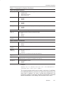
MSP430 Function Buttons and Descriptions . . . . . . . . . . . . . . . . . . . . . . . . . . . . . . . . . . . . . . 2-4
Error Messages . . . . . . . . . . . . . . . . . . . . . . . . . . . . . . . . . . . . . . . . . . . . . . . . . . . . . . . . . . . . . . . 2-8
Command Line Options . . . . . . . . . . . . . . . . . . . . . . . . . . . . . . . . . . . . . . . . . . . . . . . . . . . . . . . 2-10
MSP430 Hardware Specifications . . . . . . . . . . . . . . . . . . . . . . . . . . . . . . . . . . . . . . . . . . . . . . . 3-2
Target Connector Signal Functions . . . . . . . . . . . . . . . . . . . . . . . . . . . . . . . . . . . . . . . . . . . . . . 3-4
Programming Adapter Signal Levels . . . . . . . . . . . . . . . . . . . . . . . . . . . . . . . . . . . . . . . . . . . . . 3-4
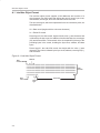
Chapter 1
This chapter describes the process of installing and programming the
hardware and software for the MSP430-PRGS430 programming adapter
used with the MSP430 family of microcontrollers.
Topic
Page
1.1
Installing the Software . . . . . . . . . . . . . . . . . . . . . . . . . . . . . . . . . . . . . . . . . 1-2
1.2
Installing the Hardware . . . . . . . . . . . . . . . . . . . . . . . . . . . . . . . . . . . . . . . . 1-3
Installation and Setup
1-1
Installing the Software
1.1 Installing the Software
To install the MSP-PRGS430 software, perform the following steps:
NOTE: To ensure that you are using the latest version of the MSP-PRGS430
software, you must download the installation executable from the TI web site.
1) Browse
to
the
MSP-PRGS430
(http://www.ti.com/prgs430).
page
on
www.ti.com
2) Go to the Support Software section and click on the link to the
MSP-PRGS430 Software (the latest version of this software can also be
downloaded from this address: http://www.ti.com/lit/zip/slac029).
3) Save the zip file to your local drive. After download is complete,
uncompress the file to extract the installation exectuable
(PRGS430_Rxxx.exe).
4) Navigate to this saved file (PRGS430_Rxxx.exe) and run it.
A welcoming message is displayed.
5) Follow the setup instructions on the screen. The setup program guides
you through the installation process.
6) During setup, the MSP430 program icons are installed in the selected
folder. Click on the PRGS430 Read Me First icon, shown in Figure 1−1,
to obtain important information about the program device hardware and
software.
Figure 1−1. ADT430 Program Icons
7) The appropriate program group and icons are added to the Windows
program manager.
8) To start the programming adapter software, click the PRGS430 icon in the
selected program group (default: ADT430).
1-2
Installing the Hardware
1.2 Installing the Hardware
To install the programming adapter hardware, perform the following steps:
1) Using the 9-pin SUB-D connector, connect the programming adapter to
the serial port (COM1−COM4) of the PC.
2) Connect an external power supply to the programming adapter. The
voltage of the power supply must be between 14 V and 20 V dc and must
provide a minimum of 200 mA of power. The center terminal of the supply
connector at the programming adapter is the plus pole.
3) The red LED on the programming adapter lights if the power supply is
properly connected. If the LED does not light and the power supply is
properly connected, check the F1 fuse on the programming adapter
printed-wire board (PWB).
4) The MSP430 devices, in a socket or on a PWB, should be connected to
the programming adapter through the 14-pin cable.
The programming adapter provides the selected supply voltage VCC at pin
14 of the 25-pin SUB-D connector, or at pin 2 of the 14-pin connector to
supply the MSP430 device. The signal name is VCC_MSP.
If an external supply voltage VCC is used for the MSP430, the internal
voltage VCC_MSP must be set to the same voltage level.
RS232
OUT
RS232 Out
May Be Connected
to an EVK
Target
(JTAG)
RS232 From PC
PC Serial Port
RS232
14−20 V
200 mA
Power Supply
MSP430 Serial Programming Adapter
MSP−PRGS430
Figure 1−2. Serial Programming Adapter
JTAG Connector
for the MSP430
Installation and Setup
1-3
1-4
Chapter 2
This chapter describes the programming procedure for MSP430 devices and
the error messages you may encounter during the procedure.
Topic
Page
2.1
Software/Hardware Layers of the PRGS430 Environment . . . . . . . . . 2-2
2.2
Programming MSP430 Devices With the GUI . . . . . . . . . . . . . . . . . . . . 2-3
2.3
Command Line Options . . . . . . . . . . . . . . . . . . . . . . . . . . . . . . . . . . . . . . 2-10
2.4
PRGS430.DLL—Description . . . . . . . . . . . . . . . . . . . . . . . . . . . . . . . . . . 2-13
Operation
2-1
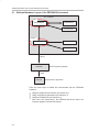
Software/Hardware Layers of the PRGS430 Environment
2.1 Software/Hardware Layers of the PRGS430 Environment
PC − Software
GUI
PRGS430.EXE
PRGS430.INI
CommandLine
Function
DEVICE.CFG
PRGS430.DLL
[Project] .INI
RS232
PRGS430
Serial Programming Adapter
JTAG
MSP430
Target Socket or Application
There are three ways to handle and communicate with the PRGS430
hardware:
- Using the graphical user interface (see Section 2.2)
- Using command line parameters (see Section 2.3)
- Using the PRGS430.dll (see Section 2.4)
Note: this is the fastest way if the PRGS430 should be used in an
in-system program and test environment.
2-2
Programming MSP430 Devices With the GUI
2.2 Programming MSP430 Devices With the GUI
2.2.1
Basic Procedure
The following steps should be used to program the MSP430 devices:
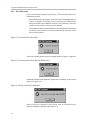
1) Click on the Program Device icon during the installation-selected program
group (default: ADT430). The MSP430 programmer dialog box appears.
The status line at the bottom of the window shows the actual or the most
recent activity (see Figure 2−1).
The status line displays the message Connecting to adapter... until the
programming adapter is detected and the baud rate is set.
2) Select the correct device and supply voltage.
3) Select the name of the object file (TI-TXT (.txt) or Intel-hex (.a43) format).
4) Select the additional options to program, if necessary using Erase Flash,
Erase Check, or Verify (see Note 1 at the end of Table 2−1).
5) Click on the Program button to start programming.
The status line at the bottom of the window shows the actual or most recent
activity (see Figure 2−1).
Figure 2−1. MSP430 Programmer Dialog Box
Operation
2-3
Programming MSP430 Devices With the GUI
2.2.2
Description of the MSP-PRGS430 GUI
An MSP430 device is commonly programmed as follows:
1) Select the file that contains the data to program from the MSP430
programmer dialog box (see Figure 2−1).
2) Select the device. An error message appears on the screen if the device
selected is different or not connected.
3) Set the required supply voltage, communication port COMx, and baud
rate. The device configuration and memory type are selected
automatically according to the selected device.
4) Use the program button to start the programming operation (see Note 1
at the end of Table 2−1).
Table 2−1 describes the function of the buttons for different options and
combinations for the MSP430 programmer dialog box.
Table 2−1. MSP430 Function Buttons and Descriptions
Button Name
Sub-Functions
Description
File Name
Selects the name of the file to program (Intel-hex or TI-TXT format)
Device Select
Selects the MSP430 device type to program via pulldown menu
Selects the supply voltage for the MSP430
Supply Voltage
VCC switch off
If selected (default), the supply voltage is switched off after each MSP430
access; otherwise, the supply voltage remains connected.
An object code is programmed to the on-chip memory using the select
options.
Program
With Erase Flash
Memory is erased before programming (only with flash devices).
The following options are possible:
− Main and information memory
− Main memory only
With Erase Check
Erase check is performed before programming operation is executed.
With Verify
Each section is verified after it is programmed, or an error message is
displayed if verification fails.
With Blow Fuse
The code-protection fuse is blown after the entire object code, with verify, is
programmed. This action is irreversible and disables future on-chip memory
access (reading or programming). This step is not performed if verify is
disabled or verify fails. A warning is displayed.
Erase operation can be done only with flash devices, according to the
selected option.
By file
Only the memory locations corresponding to the selected object file are
erased. All other memory locations keep their old data (smart erase).
By device
The entire flash memory of the device is erased.
By range
An erase is performed depending on the values entered in the range fields.
Erase Flash
Checks if memory locations are erased.
Erase Check
2-4
By file
Checks only the memory locations used by the selected object file.
By device
Checks the entire programmable memory of the device. (No RAM is
checked.)
By range
An erase check is performed according to the range of memory locations in
the range for Erase Check/Readout field.
Programming MSP430 Devices With the GUI
Table 2−1. MSP430 Function Buttons and Descriptions (Continued)
Button Name
Sub-Functions
Description
Verify the data in the MSP430 device according to the selected option.
By file
Verify
A verification of the memory locations vs the selected object file is
performed. (By file and by device are the same functions.)
By device
By range
Verify memory locations defined in the range field vs the data in the
selected file. The defined range should not contain memory locations
outside the data stored in the selected file, otherwise an error is reported.
The on-chip security fuse is irreversibly disabled and any access, such
as reading or programming of the MSP430, is impossible via JTAG.
Access via bootstrap loader interface is possible for devices that support
that interface.
Blow Fuse
Read out data from MSP430 device. When this function is executed, a
dialog box appears; the file name for the data to store should be selected.
Read Out
By device
Read out the entire memory of the device and store the data into the file
selected in the file name field.
By range
Read out the memory locations selected by the range field and store the
data in the file selected in the file name field.
The reset of a MSP430 can be performed in two ways. After reset, the
MSP430 may remain under JTAG control or can be released to operate
normally and execute the program.
Reset
PUC
A software reset of the chip is generated.
RST/NMI
Generates a hardware reset by applying a low pulse on RST/NMI pin.
With JTAG-release
JTAG is released after the execution of the reset (via JTAG or RST/NMI).
COM Port
Selects the COM port to which the programming adapter is connected
Baud Rate
Selects the baud rate for communication with the programming adapter
hardware
Help
Help is available for programming MSP430 devices, command buttons,
selectors, and the object file format used.
The Help menu can be found in the system menu of the serial
programming adapter software (right click on the symbol at the upper-left
corner of the program window) or with the F1 function key.
Note 1: For some MSP430 family members, e.g., MSP430F2xxx devices,
portions of flash information memory are factory preprogrammed with
calibration data. Depending on which method is used for erasing the flash
memory, this calibration data may be erased. Should the calibration data be
conserved, it must be read out prior to the information memory erase or a flash
erase method that does not affect the calibration data memory locations must
be used. See the respective device data sheet for further information on
preprogrammed calibration data memory locations.
If it should be saved, the following erase options must not be used as the Info
memory will be entirely erased:
− Program with Erase Flash (flash-erase options: Main and Info Memory)
or
− Erase Flash by Device
Instead, Erase Flash by File or by Range should be used.
Operation
2-5
Programming MSP430 Devices With the GUI
2.2.3
Error Messages
One of the following messages may show up if JTAG communication is not
established correctly:
If the MSP430 device to program can not be found, the message shown in
Figure 2−2 appears. This problem can be caused by the PRGS430 not
being connected to the hardware, the device not inserted or incorrectly
inserted into the socket, or the device not powered.
The problem could be that the PRGS430 is not connected to the hardware,
the device is not inserted or is incorrectly inserted into the socket, or the
device is not powered.
Figure 2−2. Communication Error Box
If the fuse is already blown, the error message shown in Figure 2−3 appears.
Figure 2−3. Communication Error Box for Blown Fuse
Additional message boxes appear for general error messages, such as erase
check (see Figure 2−4).
Figure 2−4. Erase Check Error Message
When a read error is detected in the input file, such as a format error, the
following message is displayed (see Figure 2−5).
2-6
Programming MSP430 Devices With the GUI
Figure 2−5. Data Error
Operation
2-7
Programming MSP430 Devices With the GUI
Table 2−2. Error Messages
Error Type
Error Message
Communication
Communication failed!
Communication
Adapter not connected!
Communication
Synchronization with adapter failed!
Communication
The present adapter is not an MSP-PRGS430!
Communication
Missing setting of VCC!
MSP430
Target not connected!
MSP430
Wrong JTAG version!
MSP430
PUC failed!
MSP430
Wrong target!
MSP430
Target fuse is blown!
MSP430
Blown fuse failed!
MSP430
Supply voltage to low!
MSP430
Fuse not released for this device!
Setting
Unknown target!
Setting
No target selected!
Setting
Wrong VCC selected!
Setting
Wrong baud rate!
Setting
Communication port error!
Setting
The selected range is invalid!
Setting
Wrong argument!
Setting
Error at target address (during erase check or verify)
Setting
Unknown command line option
Setting
Command line option out of valid range
System
DEVICE.CFG corrupted
System
General error!
System
File type could not be detected!
System
Unexpected end of file!
System
PROJECT.INI corrupted!
System
Filename mismatch
System
Error in DEVICE.CFG
Windows
Error during file I/O
2-8
Content of PRGS430.ini File
2.2.4
Content of PRGS430.ini File
The last settings of the PRGS430 graphical user interface (GUI) are stored in
the .ini file before exiting the program. This information is stored under the
Program Device System section.
Additionally, the following parameters are in the [Options] section and may be
modified:
[Options]
\BlowFuse = 1 → The blow fuse button in the GUI is disabled to prevent
accidental blow of the irreversible fuse.
LastResult = 0 → If the program is called with command-line parameter, the
error code which is returned to the system when exiting the program is also
stored here.
2.2.5
Use of a [Project].ini File
Some default options could be changed within a [Project].ini file. This file has
to be in the same directory as the object code file. The following variables could
be defined or redefined there.
The name of the file should have the same name as the object file with the
extension .ini.
[ProgramDevice]
UserMemProtect = Start, Size
UserMemProtect2 = Start, Size
UserMemProtect3 = Start, Size
UserMemProtectn = Start, Size
DisableTIMemProtect = 0
Memory ranges defined in the UserMemProtect and UserMemProtect [n]
option are read out and reprogrammed after erase (flash device only). [n] could
be a number ≥2 and be in ascending order.
If a memory protection is activated in the device definition file from Texas
Instruments, it could be switched off with the DisableTIMemProtect = 1 option.
Operation
2-9
Command Line Options
2.3 Command Line Options
2.3.1
General Definitions
0: Off
1: On
1: First selectable option
2: Second selectable option
3: Third selectable option
The PRGS430.ini file options are used if they are not specified in the command
line. The command line option overwrites the .ini file options.
The program exits automatically if a command is passed via the command line
and the command was executed. There is only a small status window opened
during the execution.
Only one command identifier (/cmd:) is allowed within the command line.
Otherwise, the execution is canceled and an error is returned.
If an error in the command line parameter is detected, the program exits with
an error message.
The filename may also contain a path. If special characters are used, the string
has to be inside quotes (for example, \\server\adt430\PRG files\test.txt).
If an error is detected within the filename, the operation is canceled and an
error is returned.
Table 2−3. Command Line Options
Commands:
/cmd:PRG
Program command
/cmd:VFY
Verify command
/cmd:ERS
Erase command
/cmd:CHK
Erase check command
/cmd:READ
Read out command
/cmd:RST
Reset command
/cmd:BLOW
Blow fuse command
Options:
/COM:x
Specifies the serial port: /COM:1, /COM:2, /COM:3, or /COM:4
/BR:xxxxxx
Sets baud rate to be used: 9600/19200/38400/57600/115200, e.g., /BR:57600
/Dev:
Selects the device according to the name in the device.cfg file, e.g., /Dev:MSP430F1121
/SVolt:x.x
Selects supply voltage MSP_VCC of the programming adapter. The voltage is supplied
between GND and MSP VCC, e.g., /Svolt: 3.0.
/SVoff:{0,1}
Switches off supply voltage MSP_VCC after execution
0:
Disable (do not switch off)
1:
Enable (switch off)
filename
Specifies name of the object file to be programmed or verified
/FILE filename
(Second way to define the filename − space separated)
2-10
Command Line Options
Table 2−3. Command Line Options (Continued)
Options for Program Command:
/PE:{0,1,2}
Option program with erase (flash only)
0:
Without erase
1:
Main and Info memory
2:
Main memory only
/PC:{0,1}
Option program with erase check
0:
Disable
1:
Enable
/PV:{0,1}
Option program with verify
0:
Disable
1:
Enable
/PB:{0,1}
Option program with blow fuse (only valid with verify successful)
0:
Disable
1:
Enable
Options for Erase/Erase Check and Verify Command
/E:{1,2,..}
Option erase/erasecheck/verify by file/device/range
1:
File
2:
Device
3:
Range
/ERange:0xXXX,
0xYYYY
Option erase/erasecheck/verify range (start: 0xXXXX, length: 0xYYYY)
Options for Read Out Command:
/RO:{1,2}
Option read out by device/range
1:
Device
2:
Range
/RRange:0xXXXX,
0xYYYY
Option read out range (start: 0xXXXX, length: 0xYYYY)
/Rfile:filename,{1,2}
Specifies read out file name
1:
TI-TXT
2:
Intel-hex
(Default directory should be the last object file directory)
Log Options:
/Log:filename
Specifies Log file name
(Default directory should be the PRGS430.exe directory)
/ALog:{0,1}
Option accumulative Log file
0:
Disable
1:
Enable
Example:
PRGS430.exe ”C:\adt430\test\test.txt” /Dev:MSP430F1121
/cmd:PRG /PE:1 /PC:0 /PV:1 /COM:2
This command programs the file test.txt, located in the directory C:adt430\test,
into a MSP430F149 device. The device is erased before programming. The
erase check is disabled. The code is verified after programming. The
programming adapter is connected to ComPort 2. The baud rate is not passed
with the command line, so the setting in the PRGS430.ini file is used.
Operation
2-11
2.3.2
Return Values/Error Codes in .ini File
The error code is returned to the PC operating system and also is stored in
PRGS430.ini.
File in the [Options] section:
LastResult=0
2-12
0
Ok
2
Communication failed!
3
Target not connected!
4
Adapter not connected!
5
Wrong JTAG version!
6
PUC failed!
7
Synchronization with adapter failed!
8
The present adapter is not an MSP−PRGS430!
9
Unknown target!
10
Wrong target!
11
No target selected!
12
Target fuse is blown!
13
Blow fuse failed!
14
Missing setting of VCC!
15
Wrong VCC selected!
16
Wrong baudrate!
17
Communication port error!
18
DEVICE.CFG corrupted!
19
General error!
20
The selected range is invalid!
21
Wrong argument!
22
Error during file I/O
23
File type could not be detected!
24
Unexpected end of file!
25
PROJECT.INI corrupted!
26
Vcc voltage too low for selected function!
27
Fuse not release for this device!
101
Error at target address (during erase check or verify)
102
Unknown command line option
103
Command line option out of valid range
104
Filename mismatch
105
Error in device.cfg
PRGS430.DLL—Description
2.4 PRGS430.DLL—Description
The PRGS430.dll is used to communicate with the MSP−PRGS430 hardware
and the connected MSP430 device.
The initialization of the PRGS430 should be done with the following sequence:
InitCom
SetDeviceType
SetVCC
. InitTarget
. ...
. ReleaseTarget
ReleaseCom
Several examples showing how the DLL could be used are located in the
“DLL_Usage_Examples” subdirectory of the PRGS430 system.
This dll could be used separately using the following conventions:
/FN0001/ InitCom
long int InitCom(char* lpszComPort, long int lBaudRate)
InitCom initializes (opens) the given communications port, establishes
communication with the PRGS430 hardware, and sets the baud rate of the
MSP−PRGS430. If successful, the MSP−PRGS430 is reset and VCC is set to
0.0 V (the voltage should be set after the first user action to validate the correct
value).
lBaudRate: valid baud rates are: 9600, 19200, 38400, 56800, and 115200
baud. The default baud rate after installation is 115200 baud.
lpszComPort: the name of the communication port—COM1, COM2, COM3,
or COM4.
Example: lFuncReturn = InitCom(”COM1” 115200)
/FN0002/ ReleaseCom
long int ReleaseCom (void)
This new function is the counterpart to InitCom. It allows to close a
communication with the MSP-PRGS430 hardware.
VCC is set to 0 and all outputs are set to the Hi-Z state.
Example: IFuncReturn = ReleaseComm()
/FN0003/ SetDeviceType
Example:
lFuncReturn = SetDeviceType(char* lpszDeviceName)
Selects the device type.
lpszDeviceName: name of the device in file device.cfg
Example: lFuncReturn = SetDeviceType(”MSP430F1121”)
Operation
2-13
PRGS430.DLL—Description
/FN0004/ InitTarget
long int InitTarget(char* lpszDeviceName)
Initializes the JTAG access to the target device, detects the device type, and
reports when the detected device does not match the parameter DeviceName
passed.
lpszDeviceName: name of the device in file device.cfg
Example: lFuncReturn = InitTarget (”MSP430F1121”)
/FN0005/ ReleaseTarget
long int ReleaseTarget(void)
This function performs a PUC and releases the JTAG access to the target
device. All JTAG signals from the serial programming adapter are switched to
Hi-Z. The device starts program execution if it is still connected to VCC.
Example: lFuncReturn = ReleaseTarget()
/FN0006/ Erase
long int Erase(long int wStart, long int wLength, long int Flags)
This function erases flash memory (if available). The protection of areas can
be disabled by setting the DISABLE_TI_MEM_PROTECT−Bit in Flags.
wStart: start address of the area to be erased. Allowed values :
0x0000−0xFFFE (see memory map of the corresponding device)
wLength: length of the area. Allowed values : 0x0000−0xFFFE (see the
memory map of the corresponding device)
If erasing information and main memory segments, first erase the information
memory segments, then erase the main memory segments.
The mass erase sequence then would be:
Erase(InfoStart,InfoLength,0);
Erase(MainStart,MainLength,0);
The function invokes a mass erase for information or main memory if the start
address and the complete memory range of the information or main memory
is specified. If the range specified is not complete for that device, a segment
erase of the individual segments is performed.
Flags
DISABLE_TI_MEM_PROTECT (0x01)
If this bit is set, the memory protection settings in device.cfg are ignored.
Example:
lFuncReturn = Erase(long:0xF000, long:0x1000, long:1)
2-14
PRGS430.DLL—Description
Note: For some MSP430 family members, e.g., MSP430F2xxx devices, portions of
flash information memory are factory preprogrammed with calibration data. Depending
on which method is used for erasing the flash memory, this calibration data may be
erased. Should the calibration data be conserved, it must be read out prior to the
information memory erase or a flash erase method that does not affect the calibration
data memory locations must be used. See the respective device data sheet for further
information on preprogrammed calibration data memory locations.
/FN0007/ EraseFile
long int EraseFile(char* lpszFileName, long int iFileType, long int Flags, char*
lpszProjectIni)
EraseFile() erases all addresses used in the specified file.
iFileType:
FILETYPE_AUTO
(0x00) − Autodetection of file type (Intel-hex or
TI-TXT)
FILETYPE_TI_TXT
(0x01) − File type is TI-TXT
FILETYPE_INTEL_HEX(0x02) − File type is Intel-hex
Flags:
DISABLE_TI_MEM_PROTECT (0x01)
If this bit is set, the memory protection setting device.cfg is ignored.
lpszProjectIni: name of the {project}.ini file, if protection settings from this file
shall be used. If there is no protection, replace lpszProjectIni with NULL.
Example:
lFuncReturn = EraseFile(”text.txt”, long:0, long:0,
NULL)
Note: For some MSP430 family members, e.g. MSP430F2xxx devices, portions of
flash information memory are factory preprogrammed with calibration data. Depending
on which method is used for erasing the flash memory, this calibration data may be
erased. Should the calibration data be conserved, it must be read out prior to the
information memory erase or a flash erase method that does not affect the calibration
data memory locations must be used. See the respective device data sheet for further
information on preprogrammed calibration data memory locations.
/FN0008/ EraseCheck
long int EraseCheck(long int wStart, long int wLength)
Performs an erase check of an area of the target memory
wStart: Start address of the memory area. Allowed values : 0x0000−0xFFFE
(see memory map of the corresponding device).
wLength: Size of the area. Allowed values : 0x0000−0xFFFE (see memory
map of the corresponding device)
The function EraseCheck() simply uses PatternCheck(), with 0xFFFF as
pattern.
EraseCheck(long int wStart, long int wLength)
{
return PatternCheck(wStart, wLength, 0xFFFF);
}
Example:
lFuncReturn = EraseCheck(long:0xF000, long:0x1000)
Operation
2-15
PRGS430.DLL—Description
/FN0009/ EraseCheckFile
long int EraseCheckFile(char* lpszFileName, long int iFileType)
This function checks if all memory addresses, which are in the file, are erased.
lpszFilName: Name of the file
iFileType:
FILETYPE_AUTO
(0x00) − autodetection of file type (Intel-hex or
TI-TXT)
FILETYPE_TI_TXT
(0x01) − file type is TI-TXT
FILETYPE_INTEL_HEX(0x02) − file type is Intel-hex
Function returns success or first address with mismatching data.
Example:
lFuncReturn = EraseCheckFile(”test.txt”, long:0)
/FN00010/ PatternCheck
long int PatternCheck(long int wStart, long int wLength, long int wPattern)
Checks a memory range with word pattern passed
wStart: Start address of the memory area. Allowed values : 0x0000−0xFFFE
(see memory map of the corresponding device)
wLength: Size of the area. Allowed values : 0x0000−0xFFFE (see memory
map of the corresponding device)
wPattern: Word pattern for check
Function returns success or first address with mismatching data.
Example: lFuncReturn = PatternCheck(long:0xF000,
long:0x1000, long:0xFFFF)
/FN00011/ VerifyData
long int VerifyData(long int wStart, long int wLength, void* lpData)
This function verifies the content of the device with the data stored at passed
pointer to data.
wStart: Start address of memory area. Allowed values : 0x0000−0xFFFE (see
memory map of the corresponding device)
wLength: Length of the memory area to be checked. Allowed values :
0x0000−0xFFFE (see memory map of the corresponding device)
lpData: Pointer to buffer with data bytes in it
Function returns success or first address with mismatching data.
Example:
lFuncReturn = VerifyData(long:0xF000, long:0x1000, void* lpData)
2-16
PRGS430.DLL—Description
/FN00012/ VerifyFile
long int VerifyFile(char* lpszFileName, long int iFileType)
This function checks if the memory contents of the target device are equal to
the file contents.
lpszFileName: Name of the file
iFileType
FILETYPE_AUTO
(0x00) − autodetection of file type (Intel-hex or
TI-TXT)
FILETYPE_TI_TXT
(0x01) − file type is TI-TXT
FILETYPE_INTEL_HEX(0x02) − file type is Intel-hex
Function returns success or first address with mismatching data.
Example: lFuncReturn = VerifyFile(”test.txt”, long:0)
/FN00013/ VerifyFileRange
long int VerifyFileRange(char* lpszFileName, long int iFileType, long int
wStart, long int wLength)
This function evaluates if the memory contents of the target device are equal
to the file contents in a passed range.
lpszFileName: Name of the file
iFileType:
FILETYPE_AUTO
(0x00) − autodetection of file type (Intel-hex or
TI-TXT)
FILETYPE_TI_TXT
(0x01) − file type is TI-TXT
FILETYPE_INTEL_HEX(0x02) − file type is Intel-hex
wStart: Start address of memory area. Allowed values : 0x0000−0xFFFE (see
memory map of the corresponding device)
wLength: Length of the memory area to be checked. Allowed values :
0x0000−0xFFFE (see memory map of the corresponding device)
Function returns success or first address with mismatching data.
Example: lFuncReturn = VerifyFileRange(”test.txt”,
long:0, long:0xF000, long:0x1000)
/FN0014/ ProgramData
long int ProgramData(long int wStart, long int wLength, void* lpData
This function writes data into an MSP430 device. Protection of ranges of
memory locations defined in the DEVICE.CFG file can be disabled by setting
the DISABLE_TI_MEM_PROTECT−Bit in Flags.
Operation
2-17
PRGS430.DLL—Description
wStart: Start address of the range that is to be erased. Allowed values :
0x0000−0xFFFE (see memory map of the corresponding device)
wLength: Length of the range
Allowed values : 0x0000−0xFFFE (see memory map of the corresponding device)
lpData: Pointer to the Data to be programmed
Flags: The bits in Flags control the operation of ProgramData().
Example: lFuncReturn = ProgramData(long:0xF000,
long:0x1000, void* lpData)
/FN0015/ ProgramFile
long int ProgramFile(char* lpszFileName, long int iFileType,
long int iFlags, char* lpszProjectIni)
This function writes data from the file to the MSP430 device. The protection
of ranges of memory locations defined in the DEVICE.CFG file can be disabled
by setting the DISABLE_TI_MEM_PROTECT−Bit in Flags.
If the PGM_WITH_ERASE option are not selected the program data is
preserved. This means that the data is read from the flash and replaced with
the new data. All other information is restored automatically. The handling of
the information memory works with the same mechanism.
For the fastest programming speed, select the PGM_WITH_ERASE and
PGM_ERASE_INFO options.
lpszFileName: Name of the file to be written into the target
iFileType:
FILETYPE_AUTO
(0x00) − autodetection of file type (Intel-hex or
TI-TXT)
FILETYPE_TI_TXT
(0x01) − file type is TI-TXT
FILETYPE_INTEL_HEX(0x02) − file type is Intel-hex
iFlags:
2-18
DISABLE_TI_MEMPROTECT
(0x01)
PGM_WITH_ERASE
(0x02) // Erases the main memory before
programming
PGM_ERASE_INFO
(0x04) // Erases the info memory before
programming
PGM_WITH_ERASECHECK
(0x08) // Erase check by device and the
programs the device
PGM_WITH_Verify
(0x10) // Read out device, merge with file to
be programmed, and write back to device
PRGS430.DLL—Description
Note: Use PGM_ERASE_INFO only together with the PGM_WITH_ERASE
flag.
lpszProjectIni
Name of the {project}.ini file, if protection settings from this file are used. If no
protection is required, replace lpszProjectIni with NULL.
The added features do not need to be used—for ProgramFile according to
older specification, just call ProgramFile(FileName, FileType, 0, NULL); if no
{project}.ini file or erase check is used, just call:
Example: lFuncReturn = ProgramFile(FileName, 0, 0, NULL);
autodetect file type
// with
Note: If an erase or erase-check function reports an error, the function
ProgramFile() is aborted before programming is started.
/FN0016/ BlowFuse
long int BlowFuse(void)
This function blows the security fuse of the target device.
Example: lFuncReturn = BlowFuse(void)
/FN0017/ SetVcc
long int SetVcc(long int iVoltage)
This function sets the VCC_MSP voltage of the programming adapter to the
given value.
iVoltage: VCC in mV. (3000 −> 3 V)
The correct MSP430 device should be selected before using this function.
The voltage range is limited to the voltage range allowed for the selected
MSP430 device.
Example: lFuncReturn = SetVcc(Long:3000)
/FN0018/ ReadOutData
long int ReadOutData(long int wStart, long int wLength, void* lpBuffer)
Reads out data from the device and writes it to the buffer passed
wStart: Start address of the area to be read out. Allowed values :
0x0000−0xFFFE (see memory map for the corresponding device)
wLength: Length of the area. Allowed values : 0x0000−0xFFFE (see memory
map for the corresponding device)
lpBuffer: Pointer points to a buffer that receives the data. The buffer must be
large enough to hold the entire data; otherwise, a fatal error of the operating
system may occur.
Operation
2-19
PRGS430.DLL—Description
Example: lFuncReturn = ReadOutData(long:0xF000,
long:0x1000, void* lpBuffer)
/FN0019/ ReadOutFile
long int ReadOutFile(long int wStart, long int wLength, char* lpszFileName,
long int iFileType)
Reads out data from the device and writes it to a file
wStart: Start address of the area to be read out. Allowed values :
0x0000−0xFFFE (see memory map of the corresponding device)
wLength: Length of the area. Allowed values : 0x0000−0xFFFE (see memory
map of the corresponding device)
lpszFileName: Name of the file to receive data. If the file does not exist, it is
created; If the file already exists, it is overwritten.
iFileType:
FILETYPE_TI_TXT
(0x01)
− file type is TI-TXT
FILETYPE_INTEL_HEX
(0x02)
− file type is Intel-hex
Example: lFuncReturn = ReadOutFile(long:0xF000,
long:0x1000, ”test.out”, long:1)
/FN0020/ Reset
long int Reset(long int Flags)
This function provides the reset functionality for the target.
Flags: Flags is a bitmap and determines the type of reset.
PUC
0x01
RST_NMI
0x02
WITH_RELEASE
0x04
Reset | PUC means that the JTAG sends the command to the MSP430.
Reset | RST_NMI performs a reset via the RST/NMI pin of the MSP430. The
JTAG is also reset.
If the WITH_RELEASE option is selected, the device is released from the
JTAG access after the reset.
Example: lFuncReturn = Reset(long:5)
2-20
PRGS430.DLL—Description
/FN0022/ SetNotificationWnd
LONG SetNotificationWnd(LONG hWnd, LONG IMessageID)
SetNotificationWnd() enables the status notification of a window. hWnd
passes a window handle and IMessageID passes a message identifier. Each
time a notification of the status window is necessary, the DLL sends a
IMessageID message to the hWnd window. The execution status of an
operation is passed in the WParam of this message. Completion status of the
current operation is passed (0..100) in the LParam.
The following status codes are defined:
Status
STATUS_CONNECTSPA
WParam
1
Current Operation
Connecting to SPA430
STATUS_CONNECTTARGET
3
Connecting to target
STATUS_RELEASETARGET
5
Releasing target
STATUS_RELEASESPA
7
Releasing SPA430
STATUS_RESETTARGET
9
Resetting target
STATUS_ERASE
11
Erasing target
STATUS_ERASECHECK
13
Erase checking target
STATUS_PATTERNCHECK
15
Pattern checking target
STATUS_VERIFY
17
Verifying target
STATUS_PROGRAM
19
Programming target
STATUS_READOUT
21
Reading target out
STATUS_BLOWFUSE
23
Blowing fuse
/FN0023/ GetDeviceCfgInfo
long int GetDeviceCfgInfo(long int InfoCmd, long int InfoIdx, void* lpBuf)
InfoType:
DEVICE_COUNT
(0x01)
GetDeviceCfgInfo returns number of devices in Device.cfg; InfoIdx and lpBuf
are ignored.
SELECT_DEVICE
(0x02)
Selects the given device for further commands (device number in InfoIndex,
first device is number 0; lpBuf is ignored).
DEVICE_NAME
(0x03)
Fills the name of the selected device into lpBuf; InfoIdx is ignored.
DEVICE_ID
(0x04)
Fills the DeviceID into lpBuf, InfoIdx is ignored.
DEVICE_DEFAULTOPTIONS
(0x05)
Fills the default options into lpBuf, InfoIdx is ignored.
DEVICE_MEMDEF_COUNT
(0x06)
GetDeviceCfgInfo() returns the number of memory definitions for selected
device; lpBuf and InfoIdx are ignored.
Operation
2-21
PRGS430.DLL—Description
DEVICE_MEMDEF
(0x07)
Fills the definition of a memory definition (index passed by InfoIdx) into lpBuf.
DEVICE_MEMPROTECT_COUNT(0x08)
GetDeviceCfgInfo() returns the number of memory-protection definitions for
the selected device; lpBuf and InfoIdx are ignored.
DEVICE_MEMPROTECT
(0x09)
Fills the definition of a memory protection definition (index passed by InfoIdx)
into lpBuf.
DEVICE_VCC
(0x0A)
GetDeviceCfgInfo() returns the Vcc setting for selected device in mV; lpBuf
and InfoIdx are ignored.
DEVICE_VPP
(0x0B)
GetDeviceCfgInfo() returns the Vpp setting for selected device in mV; lpBuf
and InfoIdx are ignored.
DEVICE_VFUSE
(0x0C)
GetDeviceCfgInfo() returns the blow-fuse setting for the selected device; lpBuf
and InfoIdx are ignored.
/FN0024/ AccessSFR
long int AccessSFR(LONG wAddr, void *IpData, LONG iFlags);
This function writes or reads data into the special function registers of the
MSP430 device. (implemented in PRGS320.dll versions 1.05 and higher).
wAddr: SFR address that should be accessed. Allowed values:
0x0000−0x1FE (see the memory map of the corresponding device)
IpData: Pointer to the data to be written, or buffer which should receive the read
data
Flags: The bits in Flags control the operation of AccessSFR()
iFlags:
SFR_READ
SFR_Write
(0x00)
(0x01)
Example: IFuncReturn = AccessSFR(long:0x0020, &IpData, 0)
2-22
PRGS430.DLL—Description
2.4.1
Return Values/Error Codes From PRGS430.DLL
Status
Return Value
Comment
OK
0
SUCCESS
−1
Operation OK
ERR_COMMUNICATION
−2
Communication error (SSP)
ERR_TARGET_NOT_CONNECTED
−3
No target connected
ERR_SPA430_NOT_CONNECTED
−4
No SPA430 connected
ERR_WRONG_JTAG_VERSION
−5
JTAG version above 3
ERR_PUC_FAILED
−6
PUC did not succeed
ERR_SPA430_SYNC_FAILED
−7
Could not sync SPA430
ERR_NO_SPA430
−8
Adapter is not SPA430
ERR_UNKNOWN_TARGET
−9
Target type unknown
ERR_WRONG_TARGET
−10
Target type does not match
ERR_NO_TARGET_SELECTED
−11
No target selected (missing SetDeviceType() call)
ERR_TARGET_FUSE_BLOWN
−12
No target access because of blown fuse
ERR_BLOW_FUSE_FAILED
−13
Blown-fuse command failed
ERR_VCC_NOT_SET
−14
No VCC selected (missing SetVolt() call)
ERR_WRONG_VCC
−15
VCC out of allowed range
ERR_WRONG_BAUDRATE
−16
Invalid baud rate
ERR_COMPORT
−17
Error accessing the communications port
ERR_DEVICE_CFG
−18
Device.cfg corrupted
ERR_GENERAL
−19
General error (should not occur!)
ERR_RANGE
−20
Wrong range specified
ERR_ARGUMENT
−21
Wrong argument
ERR_FILE_IO
−22
Error during file I/O
ERR_FILE_DETECT
−23
File type could not be detected
ERR_FILE_END
−24
Unexpected end of file
ERR_PROJECT_INI
−25
Error reading {project}.ini
ERR_VCC_BELOW_VCCMINPROG
−26
VCC to low for selected function
ERR_FUSE_NOT_RELEASED
−27
Fuse not release for this device
STATUS_CONNECTSPA
1
Connecting to SPA430
STATUS_CONNECTTARGET
3
Connecting to target
STATUS_RELEASETARGET
5
Releasing target
STATUS_RELEASESPA
7
Releasing SPA430
STATUS_RESETTARGET
9
Resetting target
STATUS_ERASE
11
Erasing target
STATUS_ERASECHECK
13
Erase checking target
STATUS_PATTERNCHECK
15
Pattern checking target
STATUS_VERIFY
17
Verifying target
STATUS_PROGRAM
19
Programming target
STATUS_READOUT
21
Reading out target
STATUS_BLOWFUSE
23
Blowing fuse
ERR_READOUT_LOCKED
−28
Read out prohibited
Operation
2-23
2-24
Chapter 3
This chapter describes the hardware for the MSP430 family of
microcontrollers, including specifications, components of the programming
adapters, and connection of the programming adapter to the MSP430 device
families.
Topic
Page
3.1
Specifications . . . . . . . . . . . . . . . . . . . . . . . . . . . . . . . . . . . . . . . . . . . . . . . . 3-2
3.2
Basic Hints . . . . . . . . . . . . . . . . . . . . . . . . . . . . . . . . . . . . . . . . . . . . . . . . . . . 3-2
3.3
Programming Adapter Target Connector Signals . . . . . . . . . . . . . . . . 3-3
3.4
MSP-PRGS430 Circuit Diagrams . . . . . . . . . . . . . . . . . . . . . . . . . . . . . . . 3-5
3.5
Location of Components − MSP-PRGS430 . . . . . . . . . . . . . . . . . . . . . . 3-5
3.6
Interconnection of MSP-PRGS430 to OTP/EPROM-Based
MSP430 Devices . . . . . . . . . . . . . . . . . . . . . . . . . . . . . . . . . . . . . . . . . . . . . . 3-6
3.7
Interconnection of MSP-PRGS430 to Flash-Based
MSP430 Devices . . . . . . . . . . . . . . . . . . . . . . . . . . . . . . . . . . . . . . . . . . . . . . 3-7
Hardware
3-1
Specifications
3.1 Specifications
The specifications for the MSP430 hardware are shown in Table 3−1.
Table 3−1. MSP430 Hardware Specifications
Temperature range
10°C–45°C
Humidity
40%–70%
Power supply
14 V–20 V, 200 mA minimum
Dimensions
150 mm (W) × 30 mm (H) × 95 mm (D)
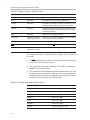
3.2 Basic Hints
These basic hints are useful for programming MSP430 devices or MSP430
devices on printed-wire boards (PWB).
- All VCC pins of an MSP430 device are tied together and connected to the
most positive terminal of the supply.
- All VSS pins of an MSP430 device are tied together and connected to the
most negative terminal of the supply.
- The interface should supply the MSP430 with proper conditions according
to the device data sheet, in terms of current, voltage levels, and timing
conditions.
- Make sure the proper signal connections (see Section 3.3) are made.
- Short cables to interconnect the interface to the MSP430 device or PWB;
less than 20 cm is recommended.
- Ensure low-impedance interconnections − especially for the path of the
programming and fuse blow voltage.
- When a device with a transparent window (MSP430E3xx family) is
programmed, the window should be already covered with an opaque label
while the device is programmed. Since ambient light contains the correct
wavelength for erasure, keep the transparent window covered after the
device is programmed.
3-2
Programming Adapter Target Connector Signals
3.3 Programming Adapter Target Connector Signals
The target connector signals for the programming adapter ensure
communication between the programming adapter and MSP430 devices and
supply low energy to systems without extra supply sources.
Figure 3−1 and Figure 3−2 show the target connector signals for the
programming adapter.
Figure 3−1. 25-Pin Sub-D at Programming Adapter
25-Pin Sub-D at the
Programming Adapter
1
TDO/TDI
14
VCC_MSP
2
TDI/Vpp
15
3
16
TMS
XOUT / TCLK
4
17
TCK
Test/VPP
5
18
GND
(ACLK)
6
RST/NMI
19
(ACLKEN)
7
20
(TCLKEN)
8
21
9
22
10
23
11
24
(SIG20)
12
25
(SMCLK)
(SMCLKEN)
13
(SENSE)
Figure 3−2. 14-Pin Connector at End of Interconnect Cable
14-Pin Connector/Female at End
of Interconnect Cable
2
1
VCC_MSP
TDO/TDI
TDI/Vpp
NC
XOUT
TMS
Test/VPP
TCK
(ACLK)
GND
RST/NMI
(ACLKEN)
(TCLKEN)
NC
14 13
Table 3−2 lists the target connector signals and describes their requirement
statuses and functions.
Hardware
3-3
Programming Adapter Target Connector Signals
Table 3−2. Target Connector Signal Functions
Signal/Terminal Name
Required
Function/Comment
TMS
Mandatory
Test mode select functions according to IEEE1149.1
TCK
Mandatory
Test clock functions according to IEEE1149.1
TDI/VPP
Mandatory
Test data input functions according to IEEE1149.1, but
with additional programming voltage for 3xx devices.
TDO/TDI
Mandatory
Test data output functions according to IEEE1149.1, but
additional data input is used when programming voltage
is applied by TDI/VPP.
GND
Mandatory
GND is the most-negative terminal.
VCC_MSP
Mandatory (if internal
supply voltage is used)
Voltage source is used with MSP430 devices or PWBs.
The voltage level is set by software.
XOUT
Mandatory
Signal supplies the MSP430 system with clock signals.
RST/NMI
Optional
If not connected, RST/NMI must be held high.
Test/VPP
Mandatory
(depending on device)
Signal used to select pin or JTAG function or to apply VPP
The output signal levels of the programming adapter are near GND or
VCC_MSP.
- The RST/NMI terminal of the device must be high; otherwise, the access
to the device via JTAG system may fail.
- The programming procedure (handling of the SW) is described in
Chapters 1 and 2 of this manual.
- The connections from the MSP430 terminals must follow EMI rules, such
as short lines and ground planes. If TMS line receives one negative pulse
by EMI strike, the fuse current is activated (with fuse version 1.0). The fuse
current flows from TDI(/VPP) pin to GND (or VSS).
Table 3−3. Programming Adapter Signal Levels
3-4
Signal/Pin
Signal/Pin Levels
TMS
VSS or VCC_MSP
TCK
VSS or VCC_MSP
TDI/VPP
VSS or VCC_MSP or VPP
TDO/TDI
VSS or VCC_MSP
XOUT
VSS or VCC_MSP
RST/NMI
VSS or VCC_MSP
Test/VPP
VSS or VCC_MSP or VPP
MSP-PRGS430 Circuit Diagrams
3.4 MSP-PRGS430 Circuit Diagrams
The MSP-PRGS430 circuit diagrams are found in Appendix B.
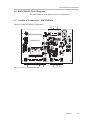
3.5 Location of Components − MSP-PRGS430
Figure 3−3. MSP-PRGS430 Components
MSP430P337
Note:
Do not use J2 pin 9 as RST/NMI pullup.
Hardware
3-5
Interconnection of MSP-PRGS430 to OTP/EPROM-Based
3.6 Interconnection of MSP-PRGS430 to OTP/EPROM-Based
MSP430 Devices
The circuit diagram in Figure 3−4 shows the connections required to program
OTP (MSP430Pxxx) and EPROM (MSP430Exxx) based MSP430 devices
with the MSP-PRGS430 programming adapter. Consult the device data sheet
for the specific device location of the supply and JTAG pins. Ensure that all
positive and negative supply pins are connected together.
Figure 3−4. MSP−PRGS430 Used to Program OTP/EPROM-Based MSP430 Devices
VCC
10 µF
0.1 µF
MSP430Pxxx
MSP430Exxx
47 kΩ
JTAG
VCC_MSP
3
4
XOUT
TEST/VPP
RST/NMI
1
2
5
6
7
8
VCC/AVCC/DVCC
10
9
12
11
14
13
TDO/TDI
TDO/TDI
TDI/VPP
TDI/VPP
TMS
TMS
TCK
TCK
GND
RST
68 kΩ
68 kΩ
TEST/VPP
XOUT
VSS/AVSS/DVSS
The RST/NMI terminal on the MSP430 device has to be held high by an
external resistor during access of the device through JTAG. In a noisy
environment, consider using an additional capacitor from RST/NMI to VSS.
Note:
The example schematic shows a system where the target voltage is supplied
by the MSP−PRGS430. For in-system programming with an external supply
voltage, do not connect pin 2 of the JTAG connector. In this case, the supply
voltage setting in the PRGS430 must be adjusted to the external supply
voltage level. The TEST/VPP connection is only required on lower pin-count
devices with multiplexed JTAG pins.
3-6
Interconnection of MSP−PRGS430 to Flash-Based MSP430 Devices
3.7 Interconnection of MSP−PRGS430 to Flash-Based MSP430 Devices
The circuit diagram in Figure 3−5 shows the connections required to program
flash-based MSP430 devices (MSP430Fxxx) with the MSP−PRGS430
programming adapter. Consult the device data sheet for the specific device
location of the power supply and JTAG pins. Ensure that all positive and
negative power supply pins are connected together.
The signal TEST/VPP is only required on lower pin-count devices with
multiplexed JTAG pins. In this case, special attention must be given to the
circuit design around the four JTAG pins (TDO/TDI, TDI, TMS, and TCK), since
they are shared between the applications hardware and the JTAG interface
used by programming adapter.
Figure 3−5. MSP−PRGS430 Used to Program Flash-Based MSP430 Devices
VCC
10 µF
0.1 µF
VCC/AVCC/DVCC
47 kΩ
JTAG
VCC_MSP
3
4
6
TEST/VPP
RST/NMI
1
2
5
7
8
MSP430Fxxx
10
9
12
11
14
13
TDO/TDI
TDI/VPP
TMS
TCK
TDO/TDI
TDI/VPP
TMS
TCK
GND
RST
TEST/VPP
VSS/AVSS/DVSS
Note:
The example schematic shows a system where the target voltage is supplied
by the MSP-PRGS430. For in-system programming with an external supply
voltage, do not connect pin 2 of the JTAG connector. In this case, the
PRGS430 supply voltage setting must be adjusted to the external supply
voltage level. The TEST/VPP connection is only required on lower pin-count
devices with multiplexed JTAG pins.
Hardware
3-7
3-8
Appendix A
This appendix discusses the hex object format.
Topic
Page
A.1
Intel-Hex Object Format . . . . . . . . . . . . . . . . . . . . . . . . . . . . . . . . . . . . . . . A-2
A.2
TI-TXT File Format . . . . . . . . . . . . . . . . . . . . . . . . . . . . . . . . . . . . . . . . . . . . A-3
Hex Object Format
A-1
Intel-Hex Object Format
A.1 Intel-Hex Object Format
The Intel-hex object format supports 16-bit addresses and consists of a
nine-character (four field) prefix that defines the start of record, byte count,
load address, record type, and a two character sumcheck suffix.
The two record types, which are represented in the nine-character prefix, are
described below:
00 = Data record (begins with the colon start character)
01 = End-of-file record
Record type 00, the data record, begins with the colon (:) start character and
is followed by the byte count, the address of the first data byte, the record type
(00), and the sumcheck. The sumcheck is the 2s complement (in binary) of the
preceding bytes in the record, including the byte count, address, and data
bytes.
Record type 01, the end-of-file record, also begins with the colon (:) start
character. The colon is followed by the byte count, address, record type (01),
and sumcheck.
Figure A−1.Intel-Hex Object Format
Start
Character
Address
:10000000FFFFFFFFFFFFFFFFFFFFFFFFFFFFFFFF00
:10001000FFFFFFFFFFFFFFFFFFFFFFFFFFFFFFFFF0
:10002000FFFFFFFFFFFFFFFFFFFFFFFFFFFFFFFFE0
:10003000FFFFFFFFFFFFFFFFFFFFFFFFFFFFFFFFD0
:10004000FFFFFFFFFFFFFFFFFFFFFFFFFFFFFFFFC0
:10000001FF
Byte
Count
A-2
Sumcheck
Record
Type
Data
Records
TI-TXT File Format
A.2 TI-TXT File Format
The TI-TXT file format used by the tool is shown as follows:
@ADDR1
DATA01
DATA02
........
DATA16
DATA17
DATA32
........
DATA32
........
DATAm
........DATAn
@ADDR2
DATA01
....................
DATAn
q
Whereas:
@ADDR is the start address of a section (hexadecimal)
DATAn represents a data byte (hexadecimal)
q is the termination of the file
For example:
@F000
31 40 00 03 B2 40 80 5A 20 01 D2 D3 22 00 D2 E3
21 00 3F 40 E8 FD 1F 83 FE 23 F9 3F
@FFFE
00 F0
Q
Restrictions:
- The number of sections is unlimited.
- The start address must be even.
- Each line must have 16 data bytes, except the last line of a section.
- Data bytes are separated by a single space.
- The termination tag q indicates end-of-file is mandatory.
Hex Object Format
A-3
A-4
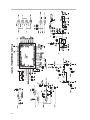
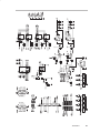
Appendix B
This appendix contains the schematic diagrams for the serial programming
adapter.
Schematics
B-1
B-2
Schematics
B-3
B-4
IMPORTANT NOTICE
Texas Instruments Incorporated and its subsidiaries (TI) reserve the right to make corrections, modifications, enhancements, improvements,
and other changes to its products and services at any time and to discontinue any product or service without notice. Customers should
obtain the latest relevant information before placing orders and should verify that such information is current and complete. All products are
sold subject to TI’s terms and conditions of sale supplied at the time of order acknowledgment.
TI warrants performance of its hardware products to the specifications applicable at the time of sale in accordance with TI’s standard
warranty. Testing and other quality control techniques are used to the extent TI deems necessary to support this warranty. Except where
mandated by government requirements, testing of all parameters of each product is not necessarily performed.
TI assumes no liability for applications assistance or customer product design. Customers are responsible for their products and
applications using TI components. To minimize the risks associated with customer products and applications, customers should provide
adequate design and operating safeguards.
TI does not warrant or represent that any license, either express or implied, is granted under any TI patent right, copyright, mask work right,
or other TI intellectual property right relating to any combination, machine, or process in which TI products or services are used. Information
published by TI regarding third-party products or services does not constitute a license from TI to use such products or services or a
warranty or endorsement thereof. Use of such information may require a license from a third party under the patents or other intellectual
property of the third party, or a license from TI under the patents or other intellectual property of TI.
Reproduction of TI information in TI data books or data sheets is permissible only if reproduction is without alteration and is accompanied
by all associated warranties, conditions, limitations, and notices. Reproduction of this information with alteration is an unfair and deceptive
business practice. TI is not responsible or liable for such altered documentation. Information of third parties may be subject to additional
restrictions.
Resale of TI products or services with statements different from or beyond the parameters stated by TI for that product or service voids all
express and any implied warranties for the associated TI product or service and is an unfair and deceptive business practice. TI is not
responsible or liable for any such statements.
TI products are not authorized for use in safety-critical applications (such as life support) where a failure of the TI product would reasonably
be expected to cause severe personal injury or death, unless officers of the parties have executed an agreement specifically governing
such use. Buyers represent that they have all necessary expertise in the safety and regulatory ramifications of their applications, and
acknowledge and agree that they are solely responsible for all legal, regulatory and safety-related requirements concerning their products
and any use of TI products in such safety-critical applications, notwithstanding any applications-related information or support that may be
provided by TI. Further, Buyers must fully indemnify TI and its representatives against any damages arising out of the use of TI products in
such safety-critical applications.
TI products are neither designed nor intended for use in military/aerospace applications or environments unless the TI products are
specifically designated by TI as military-grade or "enhanced plastic." Only products designated by TI as military-grade meet military
specifications. Buyers acknowledge and agree that any such use of TI products which TI has not designated as military-grade is solely at
the Buyer's risk, and that they are solely responsible for compliance with all legal and regulatory requirements in connection with such use.
TI products are neither designed nor intended for use in automotive applications or environments unless the specific TI products are
designated by TI as compliant with ISO/TS 16949 requirements. Buyers acknowledge and agree that, if they use any non-designated
products in automotive applications, TI will not be responsible for any failure to meet such requirements.
Following are URLs where you can obtain information on other Texas Instruments products and application solutions:
Products
Amplifiers
Data Converters
DLP® Products
DSP
Clocks and Timers
Interface
Logic
Power Mgmt
Microcontrollers
RFID
RF/IF and ZigBee® Solutions
amplifier.ti.com
dataconverter.ti.com
www.dlp.com
dsp.ti.com
www.ti.com/clocks
interface.ti.com
logic.ti.com
power.ti.com
microcontroller.ti.com
www.ti-rfid.com
www.ti.com/lprf
Applications
Audio
Automotive
Broadband
Digital Control
Medical
Military
Optical Networking
Security
Telephony
Video & Imaging
Wireless
www.ti.com/audio
www.ti.com/automotive
www.ti.com/broadband
www.ti.com/digitalcontrol
www.ti.com/medical
www.ti.com/military
www.ti.com/opticalnetwork
www.ti.com/security
www.ti.com/telephony
www.ti.com/video
www.ti.com/wireless
Mailing Address: Texas Instruments, Post Office Box 655303, Dallas, Texas 75265
Copyright © 2009, Texas Instruments Incorporated