1
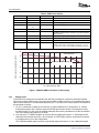
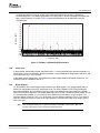
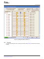
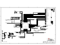
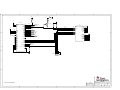
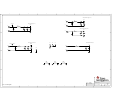
ADS5525/27/45/46/47 EVM User
Guide
User's Guide
November 2006
SLWU028B
2
SLWU028B – January 2006 – Revised November 2006
Submit Documentation Feedback
Contents
1
Overview .................................................................................................................... 5
1.1
2
3
EVM Basic Functions ............................................................................................ 5
EVM Quick Start Guide ................................................................................................ 6
2.1
EVM LVDS Output Mode Quick Start (Default) .............................................................. 6
2.2
EVM CMOS Output Mode Quick Start ........................................................................ 6
Circuit Description ...................................................................................................... 7
3.1
Schematic Diagram .............................................................................................. 7
3.2
Circuit Function ................................................................................................... 7
4
Expansion Options .................................................................................................... 13
5
........................................................................................... 13
4.2
Expansion Slot .................................................................................................. 13
4.3
Optional USB SPI Interface ................................................................................... 13
Physical Description .................................................................................................. 14
5.1
PCB Layout ...................................................................................................... 14
5.2
Bill of Materials .................................................................................................. 20
5.3
PCB Schematics ................................................................................................ 25
4.1
Custom FPGA Code
SLWU028B – January 2006 – Revised November 2006
Submit Documentation Feedback
Table of Contents
3
List of Figures
1
2
3
4
5
6
7
8
9
ADS5547 SNR Performance vs Decoupling ............................................................................. 8
THS4509 + ADS5545 EVM Performance ................................................................................ 9
Eye Diagram of Data on Header J4. ..................................................................................... 11
Top Layer.................................................................................................................... 14
Layer 2, Ground Plane .................................................................................................... 15
Layer 3, Power Plane #1 .................................................................................................. 16
Layer 4, Power Plane #2 .................................................................................................. 17
Layer 5, Ground Plane .................................................................................................... 18
Layer 6, Bottom Layer ..................................................................................................... 19
List of Tables
1
2
3
4
5
4
DIP Switch SW1 ............................................................................................................. 7
EVM Power Options ......................................................................................................... 8
Output Connector J4 ....................................................................................................... 10
Test Points .................................................................................................................. 12
Bill of Materials ............................................................................................................. 21
List of Figures
SLWU028B – January 2006 – Revised November 2006
Submit Documentation Feedback
User's Guide
SLWU028B – January 2006 – Revised November 2006
1
Overview
This manual assists users in using the ADS5525/27/45/46/47 evaluation module (EVM) for evaluating the
performance of the ADS5525/27/45/46/47 (ADCs). The EVM provides a powerful and robust capability in
evaluation of the many features of the ADCs and the performance of the device der many conditions.
1.1
EVM Basic Functions
Analog input to the ADC is provided via external SMA connectors. The user supplies a single-ended input,
which is converted into a differential signal. One input path uses a differential amplifier, while the other
input is transformer-coupled.
The EVM provides an external SMA connector for input of the ADC clock. The single-ended input is
converted into a differential signal at the input of the device.
Digital output from the EVM is via a 40-pin connector.
Power connections to the EVM are via banana jack sockets. Separate sockets are provided for the ADC
analog and digital supplies, the FPGA supply, and the differential amplifier supply.
CAUTION
Exceeding the maximum input voltages can damage EVM components.
Undervoltage may cause improper operation of some or all of the EVM
components.
Xilinx, Spartan, WebPACK are trademarks of Xilinx, Inc.
All other trademarks are the property of their respective owners.
SLWU028B – January 2006 – Revised November 2006
Submit Documentation Feedback
5
www.ti.com
EVM Quick Start Guide
2
EVM Quick Start Guide
The ADC has two basic modes of output operation, ensuring compatibility in a broad range of systems.
Follow the steps below to get the EVM operating quickly with the ADC in either DDR LVDS output mode
or CMOS output mode.
Note:
2.1
EVM LVDS Output Mode Quick Start (Default)
1.
2.
3.
4.
5.
6.
7.
8.
2.2
Ensure a jumper is installed between pins 1 and 2 on JP2.
Ensure DIP switch SW1, switch 2 is set to LVDS.
Ensure DIP switch SW1, switch 8 is set to PARALLEL.
Use a regulated power supply to provide 3.3 VDC to the ADC at J11 and J15, with the corresponding
returns connected to J9 and J16.
Use a regulated power supply to provide a 5-VDC input to J14, while connecting the return to J17.
Provide a filtered, low-phase-noise, sinusoidal 1.5-Vrms, 170-MHz clock to J7.
Provide a filtered, sinusoidal analog input to J3.
Using a logic analyzer and Table 3 in this manual, monitor the ADC output on J4.
EVM CMOS Output Mode Quick Start
1.
2.
3.
4.
5.
6.
7.
8.
9.
6
Follow the steps in the listed order; not doing so could result in improper operation.
Ensure a jumper is installed between pins 2 and 3 on JP2.
Ensure DIP switch SW1, switch 2 is set to CMOS.
Ensure DIP switch SW1, switch 8 is set to PARALLEL.
Use a regulated power supply to provide 3.3 VDC to the ADC at J11 and J15, with the corresponding
returns connected to J9 and J16.
Use a regulated power supply to provide a 5-VDC input to J14, while connecting the return to J17.
Provide a low-phase-noise, sinusoidal 1.5-Vrms, 170-MHz clock to J7.
Provide a filtered sinusoidal analog input to J3.
Briefly depress S1, which resets the EVM.
Using a logic analyzer and Table 3 in this manual, monitor the ADC output on J4.
SLWU028B – January 2006 – Revised November 2006
Submit Documentation Feedback
www.ti.com
Circuit Description
3
Circuit Description
3.1
Schematic Diagram
The schematic diagram for the EVM is in Section 5.3 of this document.
3.2
Circuit Function
The following paragraphs describe the function of individual circuits. See the data sheet for complete
device operating characteristics.
3.2.1
Configuration Options
The EVM provides a DIP switch, SW1, to control many of the modes of operation when the EVM is
configured for parallel-mode operation. Table 1 describes the functionality of the DIP switches.
Note:
When the device is configured for serial-mode operation (SW1, switch 8), the DIP settings
on SW1, switch 1 through SW1, switch 7 are ignored.
Table 1. DIP Switch SW1
SW1 SWITCH
NUMBER
OFF
ON
1
2s complement
Offset binary
Determines device output format
Determines device output mode
DESCRIPTION
2
LVDS
CMOS
3
Reserved
Reserved
4
Internal reference
External reference
5
Edge = 1
Edge = 2
Allows for output edge programmability
6
Edge = 3
Edge = 4
Allows for output edge programmability
7
Normal
Power down
8
Serial
Parallel
Reserved
When set to External Reference, ADC uses common-mode
voltage on TP1.
Allows for power down
Determines mode for register interface
By switching SW1, switch 8 to OFF, the ADC operates in serial mode, using its programmed register
contents. A complete register map can be found in the device datasheet. Three pins on header J6 have
been reserved for programming the device while it operates in serial mode. To program the device
registers using header J6, place SCLK on pin 21, SDATA on pin 23, and SEN on pin 25. A pattern
generator can be used to generate the patterns needed for programming. Alternatively, TI provides an
optional USB daughtercard that plugs into the expansion slot of the EVM. The USB daughtercard allows
ADC register control via a software package loaded onto the PC.
3.2.2
Power
Power is supplied to the EVM via banana jack sockets. The EVM offers the capability to supply analog
and digital 3.3 V independently to the ADC. Table 2 offers a snapshot of the power-supply options. All
supply connections are required for default operation, except J12, J10, J13, and J20.
The EVM provides local decoupling for the ADC; however, the ADC features internal decoupling, and in
many cases minimal external decoupling can be used without loss in performance. Users are encouraged
to experiment to find the optimal amount of external decoupling required for their application. Figure 1
shows the ADS5547 LVDS-mode performance with all of the decoupling capacitors installed and the
performance with C4, C5, C6, C7, C8, C9, and C10 removed. By default, the EVM comes with all of the
decoupling capacitors installed.
SLWU028B – January 2006 – Revised November 2006
Submit Documentation Feedback
7
www.ti.com
Circuit Description
Table 2. EVM Power Options
BANANA JACK
NAME
VOLTAGE
DESCRIPTION
J9
Device AGND
GND
J10
AGND
GND
J11
Device AVDD
3.3
Device analog supply
J12
Amplifier negative
rail
–5
THS4509 Vs– supply
J13
Amplifier positive rail
5
THS4509 Vs+ supply
J14
Auxiliary power
5
Supplies power to all peripheral circuitry including the FPGA
and PROM. Voltages rails are created by using TI's TPS75003
voltage regulator.
J15
Device DVDD
3.3
J16
DGND
GND
J17
DGND
GND
Device internal digital output supply
J20
If TP11, TP12, and TP13 are tied low, the TPS75003 is
disabled. In this case, one can supply 3.3 V to pin 1, 1.2 V to
pin 2, and 2.2 V to pin 3 of J20 while connecting the ground to
J17.
74
SNR − Signal-to-Noise Ratio − dBFS
1 Decoupling Cap
73
72
Baseline-All Decoupling Caps
71
70
69
68
9.97
19.94
30.13
40.33
50.13
60.13
69.59
79.87
89.75
100.33
130.13
170.13
fIN − Input Frequency − MHz
G001
Figure 1. ADS5547 SNR Performance vs Decoupling
3.2.3
Analog Inputs
The EVM can be configured to provide the ADC with either transformer-coupled or differential amplifier
inputs from a single-ended source. The inputs are provided via SMA connector J3 for transformer-coupled
input or SMA connector J1 for differential amplifier input. To set up for one of these options, the EVM must
be configured as follows:
1. For a 1:1 transformer-coupled input to the ADC, a single-ended source is connected to J3. Confirm
that SJP4 has pins 2 and 3 shorted, and that SJP5 has pins 2 and 3 shorted. The transformer used,
the Mini-Circuits TC4-1W, forms an inherent band-pass filter with a pass band from 3 MHz to 800 MHz.
This is the default configuration for the EVM.
2. One can use a TI THS4509 amplifier to drive the ADC by applying an input to J1. Reconfigure SJP4
and SJP5 such that both have pins 1 and 2 shorted. A 5-VDC supply must be connected to the board
to provide power to U3 for this configuration.
The THS4509 amplifier path converts a single-ended signal presented on J1 into a differential signal.
8
SLWU028B – January 2006 – Revised November 2006
Submit Documentation Feedback
www.ti.com
Circuit Description
The schematics present various interface options between the amplifier and the ADC. Depending on
the input frequencies of interest, further performance optimization can be had by designing a
corresponding filter. In its default configuration, R43, R44, and C119 form a first-order, low-pass filter
with a cutoff frequency of 70 MHz. Figure 2 shows the performance of the ADS5545 using the
THS4509 path.
10
1
0
−10
−20
Amplitude − dBFS
−30
−40
−50
−60
−70
−80
5
3
x
−90
4
−100
2
−110
−120
−130
−135
0
5
10
15
20
25
30
35
40
45
50
55
60
65
70
75
80
85
f − Frequency − MHz
G002
Figure 2. THS4509 + ADS5545 EVM Performance
3.2.4
Clock Input
A single-ended, harmonically filtered, low-phase-noise, 1.5-Vrms sinusoidal input should be applied to J7.
The frequency must not exceed the device specification. In the EVM default configuration, both SPJ1 and
SJP2 must have pins 1 and 2 shorted.
In the board default configuration, the transformer provides single-ended to differential conversion. The
transformer has an impedance ratio of 4.
3.2.5
Digital Outputs
For compatibility with a broad range of logic analyzers, the EVM outputs 3.3-V parallel CMOS data on
header J4, independent of the ADC operational mode. The Xilinx™Spartan™-3E FPGA provides the
necessary translation, and it configures itself using one of two different logic files stored in the PROM,
based on the EVM configuration. The CMOS data output of the FPGA is contained in data header J4 and
is a standard 40-pin header on a 100-mil grid, which allows easy connection to a logic analyzer. The
connector pinout is listed in Table 3. For quick setup, the eye diagram is shown in Figure 3. No setup or
hold-time adjustments must be made to the logic analyzer if using the rising edge of the output clock to
latch in the data.
Note:
The eye diagram shown is the output of the FPGA at 210 MSPS, not that of the ADC. For
the ADC output timing, see the respective device data sheet.
SLWU028B – January 2006 – Revised November 2006
Submit Documentation Feedback
9
www.ti.com
Circuit Description
Table 3. Output Connector J4
J4 PIN
10
ADS5525/27 DESCRIPTION
ADS5545/46/47 DESCRIPTION
1
CLK
CLK
2
GND
GND
3
NC
NC
4
GND
GND
5
Reserved
Reserved
6
GND
GND
7
Reserved
Reserved
8
GND
GND
9
NC
Data bit 0 (LSB)
10
GND
GND
11
NC
Data bit 1
12
GND
GND
13
Data bit 0 (LSB)
Data bit 2
14
GND
GND
15
Data bit 1
Data bit 3
16
GND
GND
17
Data bit 2
Data bit 4
18
GND
GND
19
Data bit 3
Data bit 5
20
GND
GND
21
Data bit 4
Data bit 6
22
GND
GND
23
Data bit 5
Data bit 7
24
GND
GND
25
Data bit 6
Data bit 8
26
GND
GND
27
Data bit 7
Data bit 9
28
GND
GND
29
Data bit 8
Data bit 10
30
GND
GND
31
Data bit 9
Data bit 11
32
GND
GND
33
Data bit 10
Data bit 12
34
GND
GND
35
Data bit 11 (MSB)
Data bit 13 (MSB)
36
GND
GND
37
NC
NC
38
GND
GND
39
NC
NC
40
GND
GND
SLWU028B – January 2006 – Revised November 2006
Submit Documentation Feedback
www.ti.com
Circuit Description
C001
Figure 3. Eye Diagram of Data on Header J4.
3.2.6
Test Points
For added EVM visibility and control, several test points are provided. Table 4 summarizes the test points
available.
SLWU028B – January 2006 – Revised November 2006
Submit Documentation Feedback
11
www.ti.com
Circuit Description
Table 4. Test Points
TP
3.2.7
DESCRIPTION
TP1
ADC common mode, input or output
depending on the setting of SW1, switch 4
TP3
THS4509 power down
TP4
ADC output enable
TP5
AGND
TP6
AGND
TP7
AGND
TP8
DGND
TP9
FPGA M0 pin; determines which FPGA logic
file to load
TP10
ADC SCLK
TP11
TPS75003 1.2 enable
TP12
TPS75003 2.5 enable
TP13
TPS75003 3.3 enable
LED Operation
To give greater visibility into the EVM operations, two LEDs are provided, D3 and D4. On power up, D4 is
asserted when a successful FPGA boot up is complete. For correct EVM operation, the LED should be
asserted at all times. LED D3 is asserted when the ADC and FPGA are operating and decoding in DDR
LVDS mode, and is not asserted when the ADC is functioning in CMOS mode. Furthermore, in either DDR
LVDS mode or CMOS mode, LED D3 blinks when an ADC overrange condition occurs.
CAUTION
If LED D3 is blinking, the amplitude coming into the ADC input (J3 or J4) must
be attenuated immediately; otherwise, damage to the ADC could occur.
12
SLWU028B – January 2006 – Revised November 2006
Submit Documentation Feedback
www.ti.com
Expansion Options
4
Expansion Options
The EVM offers several exciting possibilities to expand the capabilities of the EVM. This allows the utmost
flexibility when prototyping an ADC circuit under conditions that mimic the end system, without the need to
develop a custom prototype board.
4.1
Custom FPGA Code
Using a standard JTAG interface on JP1, users have the ability to load custom logic onto the FPGA,
rapidly speeding up digital development time. This allows the flexibility of prototyping and debugging an
ADC digital interface design before developing application-specific hardware.
To take advantage of the onboard FPGA, users can download the free Xilinx WebPACK™ from the Xilinx
Web site. Select the XC3S250E-4FT256 as the FPGA and the XCF16PFSG48 as the PROM.
Note:
See the Xilinx Spartan-3E Web site for complete documentation of the FPGA at:
http://direct.xilinx.com/bvdocs/publications/ds312.pdf
Schematically, the FPGA is configured in BPI mode, and it samples FPGA pins M2, M1, and M0 when the
FPGA's INIT_B is brought low. Depending of the status of M0, it boots from either the top or the bottom of
the PROM contents. The PROM allows for the storage of two FPGA bit files. In its default condition, the
EVM stores one file for ADC CMOS output at the beginning of the PROM address space and one file for
ADC LVDS output at the end of the PROM address space.
Note:
4.2
When creating custom FPGA code, store any custom-developed bit files for ADC CMOS
operation in the PROM revision 0 space, and store any custom-developed FPGA code for
ADC LVDS operation in the PROM revision 1 space.
Expansion Slot
For those users who make use of a custom FPGA program on the EVM, J5 and J6 provide an
expansion-slot capability. Users can design daughtercards or breakout boards to make use of the unused
FPGA I/O pins which are brought out to the headers.
Note:
4.3
The EVM provides 5 V from J14 to pin 1 of both J5 and J6. This can be used to provide
power to any designed daughtercards.
Optional USB SPI Interface
In most cases, users can use the ADC parallel interface mode to change the operational modes of the
ADC. For users requiring SPI control of the ADC, TI has developed an optional USB daughter card that
plugs into the expansion slot. With the USB daughter card, users can use a PC interface to communicate
to the ADC three-wire SPI interface, which allows for complete control of the ADC register map. Contact
the factory for this optional accessory.
SLWU028B – January 2006 – Revised November 2006
Submit Documentation Feedback
13
www.ti.com
Physical Description
5
Physical Description
This chapter describes the physical characteristics and PCB layout of the EVM.
5.1
PCB Layout
The EVM is constructed on a 6-layer, 0.062-inch thick PCB using FR-4 material. The individual layers are
shown in Figure 4 through Figure 9. The layout features split analog and digital ground planes; however,
similar performance can be had with careful layout using a single ground plane. Users can connect the
analog and digital ground planes underneath the EVM by soldering the two exposed tinned strips together.
K001
Figure 4. Top Layer
14
SLWU028B – January 2006 – Revised November 2006
Submit Documentation Feedback
www.ti.com
Physical Description
K002
Figure 5. Layer 2, Ground Plane
SLWU028B – January 2006 – Revised November 2006
Submit Documentation Feedback
15
www.ti.com
Physical Description
K003
Figure 6. Layer 3, Power Plane #1
16
SLWU028B – January 2006 – Revised November 2006
Submit Documentation Feedback
www.ti.com
Physical Description
K004
Figure 7. Layer 4, Power Plane #2
SLWU028B – January 2006 – Revised November 2006
Submit Documentation Feedback
17
www.ti.com
Physical Description
K005
Figure 8. Layer 5, Ground Plane
18
SLWU028B – January 2006 – Revised November 2006
Submit Documentation Feedback
www.ti.com
Physical Description
K006
Figure 9. Layer 6, Bottom Layer
SLWU028B – January 2006 – Revised November 2006
Submit Documentation Feedback
19
www.ti.com
Physical Description
5.2
20
Bill of Materials
SLWU028B – January 2006 – Revised November 2006
Submit Documentation Feedback
www.ti.com
Physical Description
Table 5. Bill of Materials
VALUE
FOOTPRINT
QTY
PART NUMBER
VENDOR
DIGI-KEY NUMBER
REF DESIGNATOR
NOT
INSTALLED
CAPACITORS
47-µF, tantalum, 20%, 10-V
7343
4
ECS-T1AD476R
Panasonic
PCS2476CT-ND
C65, C66, C68, C69
10-µF, 10-V, 20%
3528
5
ECS-T1AX106R
Panasonic
PCS2106CT-ND
C70, C71, C72, C73,
C74
10-µF, 10-V, 20%
3216
2
ECS-T1AY106R
Panasonic
P11309CT-ND
C8, C9
100-µF, 6.3-V, 10%
6032
2
TPSC107K006R0150
AVX
478-1764-2-ND
C35, C60
0.1-µF, 16-V, 10%
805
2
ECJ-2VB1C104K
Panasonic
PCC1812CT-ND
C115, C116
2.2-µF, 6.3-V, 10%
805
1
ECJ-GVB0J225K
Panasonic
PCC2310CT-ND
C117
10-µF, 6.3-V, 10%
805
4
GRM21BR60J106KE19L
Murata
490-1717-1-ND
C13, C30, C40, C41
0.01-µF, 16-V, 10%
603
1
ECJ-1VB1C103K
Panasonic
PCC1750CT-ND
C57
0.1-µF, 16-V, 10%
603
18
ECJ-1VB1C104K
Panasonic
PCC1762CT-ND
C14,
C26,
C33,
C38,
C62,
1.5-nF, 50-V, 10%
603
3
C1608X7R1H152K
TDX
10-pF, 50-V, ±0.5-pF
603
1
ECJ-1VC1H100D
Panasonic
PCC100CVCT-ND
C53
1-µF, 6.3-V, 10%
603
1
ECJ-1VB0J105K
Panasonic
PCC1915CT-ND
C64
10-µF, 6.3-V, 20%
603
1
ECJ-1VB0J106M
Panasonic
PCC2395CT-ND
C63
100-µF, 4-V, 20%
603
1
NOJC107M004RWJ
AVX
478-1824-1-ND
C61
2.2-µF, 6.3-V, 10%
603
13
ECJ-1VB0J225K
Panasonic
PCC2273CT-ND
C85–C96, C114
18-pF, 50-V, 5%
603
1
GRM1885C1H180JA01D
Murata
490-1409-1-ND
C119
2-pF, 100-V, ±0.25-pF
603
0
GQM1885C2A2R0CB01D
Murata
490-3555-1-ND
0.1-µF, 16-V, +80/–20%
402
14
ECJ-0EF1C104Z
Panasonic
PCC1731CT-ND
C1, C3, C4, C5, C6,
C7, C10, C11, C12,
C16, C17, C19, C29,
C44, C49
0.22-µF, 6.3-V , ±10%
402
17
ECJ-0EB0J224K
Panasonic
PCC2269CT-ND
C42,
C50,
C76,
C80,
C84
0.022-µF, 6.3-V, +80/–20%
201
16
02016G223ZAT2A
AVX
478-1054-1-ND
C97, C98, C99, C100,
C101, C102, C103,
C104, C105, C106,
C107, C108, C109,
C110, C111, C112
SLWU028B – January 2006 – Revised November 2006
Submit Documentation Feedback
C15, C18,
C27, C28,
C34, C36,
C39, C51,
C113
C25,
C32,
C37,
C55,
C52
C31, C58, C59
C2, C118
C20
C43,
C54,
C77,
C81,
C46,
C67,
C78,
C82,
C48,
C75,
C79,
C83,
21
www.ti.com
Physical Description
Table 5. Bill of Materials (continued)
VALUE
FOOTPRINT
QTY
PART NUMBER
VENDOR
DIGI-KEY NUMBER
REF DESIGNATOR
ERJ-3GEY0R00V
Panasonic
P0.0GCT-ND
R5, R6, R10, R18,
R48, R58, R82
R11, C45, C47
NOT
INSTALLED
RESISTORS
0-Ω, 1/10-W, 5%
603
7
0-Ω, 1/10-W, 5%
402
3
ERJ-GE0R00X
Panasonic
P0.0JCT-ND
4.02-Ω, 1/10-W 1%
603
2
9C06031A4R02FGHFT
Yageo
311-4.02HCT-ND
20-Ω, 1/16-W, 1%
603
1
ERJ-3EKF20R0V
Panasonic
P20.0HCT-ND
R79
24.9-Ω, 1/16-W, 1%
603
1
ERJ-3EKF24R9V
Panasonic
P24.9HCT-ND
R17
4.7-Ω, 1/2-W, 5%
603
2
ERD-S1TJ4R7V
Panasonic
P4.7BBCT-ND
R44, R47
36-Ω, 1/10-W, 1%
603
0
RC0603FR-0736RL
Yaego
311-36.0HRCT-ND
49.9-Ω, 1/16-W, 1%
603
2
ERJ-3EKF49R9V
Panasonic
P49.9HCT-ND
R35, R36
100-Ω, 1/16-W, 0.1%
603
3
ERA-3YEB100V
Panasonic
P100YCT-ND
R31, R41, R60
200-Ω, 1/16-W, 1%
603
2
ERJ-3EKF2000V
Panasonic
P200HCT-ND
R15, R16
330-Ω, 1/16-W, 5%
603
3
ERA-V33J331V
Panasonic
P330CHCT-ND
499-Ω, 1/16-W, 1%
603
2
ERJ-3EKF4990V
Panasonic
P499HCT-ND
10-kΩ, 1/16-W, 1%
603
11
ERJ-3EKF1002V
Panasonic
P10.0KHCT-ND
R2, R3, R4, R7, R8,
R9, R26, R32, R33,
R39, R40
4.75-kΩ, 1/16-W, 1%
603
2
ERJ-3EKF4751V
Panasonic
P4.75KHCT-ND
R46, R49
15.4-kΩ, 1/16-W, 1%
603
1
ERJ-3EKF1542V
Panasonic
P15.4KHCT-ND
R65
20-kΩ, 1/16-W, 1%
603
3
ERJ-3EKF2002V
Panasonic
P20.0KHCT-ND
R30, R80, R81
36.5-kΩ, 1/16-W, 1%
603
1
ERJ-3EKF3652V
Panasonic
P36.5KHCT-ND
R66
56.2-kΩ, 1/16-W, 1%
603
1
ERJ-3EKF5622V
Panasonic
P56.2KHCT-ND
R1
4.99-kΩ, 1/16-W, 1%
603
3
ERJ-3EKF4991V
Panasonic
P4.99KHCT-ND
R27, R28, R29
61.9-kΩ, 1/16-W, 1%
603
2
ERJ-3EKF6192V
Panasonic
P61.9KHCT-ND
R63, R64
0.033-Ω, 1/4-W, 5%
805
2
RL1220T-R033-J
Susumu Co,. Ltd.
RL12T.033JCT-ND
R61, R62
348-Ω, 1/16-W, 1%
402
2
ERJ-2RKF3480X
Panasonic
P348LCT-ND
R24, R25
49.9-Ω, 1/16-W, 1%
402
3
ERJ-2RKF49R9X
Panasonic
P49.9LCT-ND
R19, R42, R43
78.7-Ω, 1/16-W, 1%
402
2
ERJ-2RKF78R7X
Panasonic
P78.7LCT-ND
R20, R21
100-Ω, 1/16-W, 1%
402
2
ERJ-2RKF1000X
Panasonic
P100LCT-ND
R22, R23
20-Ω R-pack, 5%, 0.063-W
CTS-742_8RES
2
742C163220JTR
CTS
742C163220JCT-ND
RP1, RP2
10-kΩ resistor pack
CTS_742_8RES
1
742C163103JTR
CTS
742C163103JCT-ND
RP3
22
R54, R56
R37, R38
R12, R13
R34, R59
R85, R86
R45, R87, R88
R83, R84
SLWU028B – January 2006 – Revised November 2006
Submit Documentation Feedback
www.ti.com
Physical Description
Table 5. Bill of Materials (continued)
VALUE
FOOTPRINT
QTY
PART NUMBER
VENDOR
DIGI-KEY NUMBER
REF DESIGNATOR
NOT
INSTALLED
FERRITE BEADS, CONNECTORS, JUMPERS, JACKS, ICs, ETC.
Ferrite bead
1206
5
Inductor, SMT, 15-µH, 2.6-A
COIL-CDRH8D43
Inductor, SMT, 5-µH, 2.9-A
COIL-CDRH6D38
0.0-Ω, 1/8-W, 5% resistor
EXC-ML32A680U
Panasonic
P10437CT-ND
1
CDRH8D43-150
Sumida
1
CDRH6D38-5R0
Sumida
CDRH6D38-5R0NC-ND
FB2, FB3, FB4, FB6,
FB7
L1
L2
805
2
ERJ-6GEY0R00V
Panasonic
P0.0ACT-ND
Red test point
Test_point2
8
5000k
Keystone
5000K-ND
TP1, TP4, TP9, TP10
Black test point
Test_point2
4
5001k
Keystone
5000K-ND
TP5 TP6 TP7 TP8
20×2×.1
1
HTSW-120-07-L-D
Samtec
J4
40-pin header smt
20X2_SMT_MMS_
SAMTEC
2
MMS-120-02-T-DV
Samtec
J5, J6
Red banana jacks
BANANA_JACK
5
ST-351A
Allied
N/A
J11, J12, J13, J14,
J15
Black banana jacks
BANANA_JACK
4
ST-351B
Allied
N/A
J9, J10, J16, J17
ARFX1231-ND
40-pin header
SMA connectors
3POS_header
6-pin header
L3, L4
SMA_Jack
3
901-144-8RFX
AMP
3pos_jumper
1
HTSW-150-07-L-S
Samtec
JP2 (1)
JP1
6×1×.1
1
HTSW-120-07-L-D
Samtec
3-pin power connector
3term_screw_con
0
93F7124
Newark
Transformer
TC4-1W_
TRANSFORMER
3
TC4-1W
Mini-Circuits
Diode, Schottky, 1-A, 20-V
DIODE-MBRM120
1
MBRM120E
ON Semiconductor
Diode, Schottky, 3-A, 20-V
J1, J3, J7
D2
1
SS32
Vishay
LED-1206
2
CMD15-21VGC/TR8
Panasonic
MOSFET, P-CH, 20-V, 4.7-A,
39-MΩ
3-SOT-23
2
SI2323DS
Vishay
TRANS BIAS NPN, 50-V
SOT416
1
DTC114EET1
ON Semiconductor
DTC114EET1OS-ND
Q3
Switch
EVQ-PJ
1
EVQ-PJX04M
Panasonic
P8050SCT-ND
S1
Switch, 8-Pos, half-pitch SMT
SWITCH_8POS_
SMT
1
TDA08H0SK1
ITT
CKN1365-ND
SW1
3-circuit jumpers
SJP3_RESISTOR
2
ERJ-3GEY0R00V
Panasonic
P0.0GCT-ND
SJP4 (2), SJP5 (3)
3-circuit jumpers
SJP3_402
2
ERJ-2GE0R00X
Panasonic
P0.0JCT-ND
SJP1 (4), SJP2 (5)
(use a 0-Ω resistor
(use a 0-Ω resistor
(use a 0-Ω resistor
(use a 0-Ω resistor
SLWU028B – January 2006 – Revised November 2006
Submit Documentation Feedback
to
to
to
to
short
short
short
short
J8
T1, T2, T3
DO-214AB(SMC)
Add jumper for JP2 between pins 1 to 2.
Add jumper for SJP4 between pins 2 and 3
Add jumper for SJP5 between pins 2 and 3
Add jumper for SJP1 between pins 1 and 2
Add jumper for SJP2 between pins 1 and 2
TP3 TP11
TP12 TP13
J20
Green SM_LED_1206
(1)
(2)
(3)
(4)
(5)
FB8, FB9,
FB10
D1
L62205CT-ND
D3, D4
Q1, Q2
pins).
pins).
pins).
pins).
23
www.ti.com
Physical Description
Table 5. Bill of Materials (continued)
VALUE
FOOTPRINT
ADS5525/27, ADS5545/46/47
48-QFN_MOD
Spartan-3E XC3S250E
256-BGA1mm_XILINX
IC amp, fully-diff, wideband
16-QFN(RGT)
1
XCF16PFSG48
QTY
1
PART NUMBER
VENDOR
DIGI-KEY NUMBER
ADS5525/27,
ADS5545/46/47
TI
U1
XC3S250E-4FT256CES
Xilinx
U2
THS4509RGTT
TI
296-17730-1-ND
REF DESIGNATOR
U3
48PIN_BGA_XILINX
1
XCF16PFSG48
Xilinx
IC, pwr-mgmt, triple-supply
20-pin-QFN
1
TPS75003RHLR
TI
296-17835-2-ND
U6
IC, LDO reg, hi-PSRR, 1.8-V
5-SOT(DBV)
1
TPS73018DBVT
TI
296-17577-1-ND
U7
IC, comparator, R-R, hi-spd
8-TSSOP(DCN)
1
TLV3502AIDCNT
TI
296-18147-2-ND
U9
5-SOT(DBV)
1
SN74LVC1G86DBVR
TI
296-9853-1-ND
U10
Shorting jumper
1
N/A
3M
929955-06-ND
Screw
4-40 × 3/8"
4
N/A
Building Fasteners
H781-ND
Standoff, hex (1/4 x .5")
4-40 screw
4
N/A
Keystone
1902CK-ND
IC, EX-OR gate, 2-in
2-pos shunt
24
NOT
INSTALLED
U4
SLWU028B – January 2006 – Revised November 2006
Submit Documentation Feedback
www.ti.com
Physical Description
5.3
PCB Schematics
The schematics for the EVM are on the following pages.
SLWU028B – January 2006 – Revised November 2006
Submit Documentation Feedback
25
U2A
XILINX XC3S500E_FT256
DRVDD
D
C3
C1
.1uF
.1uF
+
C8
10uF
CLKOUTM
CLKOUTP
AVDD
+
C9
C4
C5
C6
C7
C10
C19
10uF
.1uF
.1uF
.1uF
.1uF
.1uF
.1uF
D12_D13P
D12_D13M
A9
A10
D10_D11P
D10_D11M
D8_D9P
D8_D9M
D6_D7P
D6_D7M
D4_D5P
D4_D5M
B8
A8
D8
C8
D7
E7
D6
C6
E6
D5
A4
A5
C4
C5
B3
C3
A3
C13
C12
D12
C9
C10
D2_D3P
D2_D3M
U1-H6
(Sh 4)
U1-H5
U1-H6
U1-H5
3.3V
R3
R27
R30
10K
4.99K
20K
(Sh 4)
DFS
DFS
(Sh 4)
(Sh 4)
OE
CLKP
CLKM
OVR
CLKOUTM
CLKOUTP
R10
OE
0
TP4
CLKP
CLKM
DRGND
DRVDD
OVR
CLKOUTM
CLKOUTP
DFS
OE
AVDD
AGND
CLKP
CLKPM
AGND
U1
ADS5545_48PIN-QFN
DRGND
DRVDD
D0_D1P
D0_D1M
N/C
N/C
RESET
SCLK
SDATA
SEN
AVDD
AGND
36
35
34
33
32
31
30
29
28
27
26
25
A7
A12
B4
B6
B10
TP10
D0_D1P
D0_D1M
D9
R41
R48
R6
100 RESET
SCLK
SDATA
0
0
R18
0
S1
CM
AGND
INP
INM
AGND
AVDD
AGND
AVDD
IREF
AVDD
MODE
AVDD
(Sh 4)
(Sh 4)
OVR
1
2
3
4
5
6
7
8
9
10
11
12
D12_D13P
D12_D13M
D10_D11P
D10_D11M
D8_D9P
D8_D9M
D6_D7P
D6_D7M
D4_D5P
D4_D5M
D2_D3P
D2_D3M
48
47
46
45
44
43
42
41
40
39
38
37
C
(Sh 4)
RESET
SCLK
SDATA
(Sh 4)
(Sh 4)
(Sh 4)
R81
R29
R7
20K
4.99K
10K
1
JP2
(1-2)
3.3V
D
IP_L10N_0/GCLK9
IP_L10P_0/GCLK8
IO_L11N_0/GCLK11
IO_L11P_0/GCLK10
IO_L14N_0/VREF_0
IO_L14P_0
IO_L15N_0
IO_L15P_0
IP_L16N_0
IP_L16P_0
IO_L17N_0/VREF_0
IO_L17P_0
IO_L18N_0
IO_L18P_0
IO_L19N_0/HSWAP
IO_L19P_0
IP
IP
IP_L02N_0
IP_L02P_0
IP_L07N_0
IP_L07P_0
NC
NC
GND
GND
GND
GND
GND
GND
GND
IO
IO
IO
IP
IP
C7
B7
C
A1
B9
F6
G7
G8
G9
H8
IO_VREF_0
U1-G2
(Sh 4)
U1-G3
(Sh 4)
SEN
(Sh 4)
DRVDD
SW-PB
SEN
R2
10K
13
14
15
16
17
18
19
20
21
22
23
24
VCCO_0
B5
B12
F7
F10
2
IO_L09N_0/GCLK7
IO_L09P_0/GCLK6
U1-G3
3.3V
2.5V
VCCO_0
VCCO_0
VCCO_0
VCCO_0
IO_L04P_0
IO_L05N_0/VREF_0
IO_L05P_0
IO_L06N_0
IO_L06P_0
IO_L12N_0
IO_L12P_0
IO_L08N_0/GCLK5
IO_L08P_0/GCLK4
U1-G2
U1-H4
B
IO_L01N_0
IO_L01P_0
IO_L03N_0/VREF_0
IO_L03P_0
2.5V
IO_L04N_0
3
A14
B14
A13
B13
E11
D11
B11
C11
E10
D10
F8
E8
F9
E9
U1-H3
3.3V
DRVDD
R80
R28
R4
20K
4.99K
10K
U1-H4
(Sh 4)
U1-H3
(Sh 4)
MODE
(Sh 4)
B
TP1
(Sh 2) VCM
R32
DFS
3.3V
10K
(Sh 2)
3.3V
CM
VCM
R5
0
MODE
CM
C14
10K
2
3
4
2.2uF
+IN A
V+
-IN A
OUT A
+IN B
OUT B
-IN B
V-
8
7
10K
A
56.2K
TP9
U10
1
4
6
R1
.1uF
2
SN74LVC1G86
5
3
R39
.1uF
IREF
C116
5
1
C117
.1uF
U9
TLV3502
R33
C115
M0
M0
(Sh 4)
(Sh 2)
INP
(Sh 2)
INM
INP
INM
ti
R40
10K
A
12500 TI Boulevard. Dallas, Texas 75243
Title:
Engineer:
Note 1. Part not installed
Drawn By:
FILE:
J. VENABLE
Y. DEWONCK
SIZE:
ADS5545
DATE:
11-Jul-2006
REV:
B
1
SHEET:
OF:
7
1
2
3
4
5
6
+VCC
AMPLIFIER PATH:
C11
C12
.1uF
.1uF
C13
C40
10uF
AC Couple (default)
10uF
C45 C47 = 0.1uF
R26 R27 = 200 Ohms
R5 = 0 Ohms
VCC= 5 V, VEE = GND
R24
348
D
D
TP3
DC Couple
.1uF
VCM
7
8
R44
L3
49.9
R85
0 ohm
Vs+
Vs+
0 ohm
C2
4.7
200
20pF
C47
Vin+
Vout-
R43
10
CM
C119
CM
L4
49.9
C118
0 ohm
0 ohm
CM
C49
20pF
R86
R47
20pF
200
AMP_M
4.7
16
499
15
R21
14
R84
.1uF
9
.1uF
R42
THS4509
4
C16
U3
Vin-
11
VCM
AMP_P
C45
3
Vs-
499
Vout+
Vs-
R83
69.8
N/C
2
Vs-
R20
Vs+
PD
5
4
3
2
1
Vs+
100
(Sh 1)
C45 C47 = 0 Ohms
R26 R27 = Unpopulated
R5 = Unpopulated
VCC= 4 V, VEE = -1V
R22
Vs-
C44
13
1
6
12
SMA_END
5
J1
69.8
C
R23
R25
100
348
C
-VCC
R19
49.9
C46
C17
C29
C30
C41
.1uF
.1uF
10uF
10uF
.22uF
Note : R12, C20, and R13 are to be un-populated
on ADS5525/45/46 EVMs.
24.9
R12, C20, and R13 may be populated for
future ADC boards; contact factory for details.
AMP_M
CM
CM
B
1
R17
B
SJP4
R37
2
INM
(Sh 1)
4.02
(2-3)
R12
36
3
J3
AIN
INM
C15
5
4
3
2
1
4
T1
R34
49.9
(Note 1)
3
1
2
6
R15
R16
200
200
1
T2
6
.1uF
2
C113
3
TC4-1W
R35
R36
49.9
49.9
C52
C20
2pF
.1uF
(Note 1)
4
TC4-1W
AMP_P
.1uF
R13
36
1
C55
C62
C51
.1uF
.1uF
SJP5
2
.1uF
INP
INP
(Sh 1)
4.02
3
(2-3)
R38
ti
A
A
12500 TI Boulevard. Dallas, Texas 75243
Title:
Engineer:
Note 1. Part not1installed
2
3
4
5
Drawn By:
FILE:
J. VENABLE
Y. DEWONCK
ADS5545
DOCUMENTCONTROL #
REV:
6
DATE:
17-Jul-2006
SIZE:
SHEET:
2
OF:
B
7
1
2
3
4
5
6
D
D
1
(Note 1)
J7
CLK_INP
R54
2
0
C25
6
T3
1
5
4
3
2
R59
2
49.9
(Note 1)
4
100
.1uF
SJP2
3
2
CLKP
CLKP
(Sh 1)
0
C26
.1uF
3
(1-2)
R56
1
(Note 1)
1
R58
5
4
3
2
R31
100
TC4-1W
J8
CLK_INM
(Note 1)
R60
1
1
0
2
SJP1
CLKM
CLKM
(Sh 1)
3
(1-2)
C
C
B
B
ti
A
A
12500 TI Boulevard. Dallas, Texas 75243
Title:
Note 1. Part not installed
Engineer:
J. VENABLE
Drawn By:
Y. DEWONCK
FILE:
1
2
3
4
5
ADS5545
DOCUMENTCONTROL #
DATE:
11-Jul-2006
SIZE:
6
SHEET:
3
REV:
B
OF:
7
1
2
3
4
5
U2B
XILINX XC3S500E_FT256
5V
J5
J4
2
4
6
8
10
12
14
16
18
20
22
24
26
28
30
32
34
36
38
40
D
R79
1
3
5
7
9
11
13
15
17
19
21
23
25
27
29
31
33
35
37
39
CLKOUT
20
RP1
20 Ohm
1
2
3
4
5
6
7
8
1
2
3
4
5
6
7
8
16
15
14
13
12
11
10
9
16
15
14
13
12
11
10
9
2
4
6
8
10
12
14
16
18
20
22
24
26
28
30
32
34
36
38
40
ADC_D0
ADC_D1
ADC_D2
ADC_D3
ADC_D4
ADC_D5
ADC_D6
ADC_D7
ADC_D8
ADC_D9
ADC_D10
ADC_D11
ADC_D12
ADC_D13
ADC_D14
ADC_D15
RP2
20 Ohm
40PIN_IDC
1
3
5
7
9
11
13
15
17
19
21
23
25
27
29
31
33
35
37
39
(Sh 5)
IO/HDC
CTRL_LE
CTRL_DATA
CTRL_CLK
C
U2C
XILINX XC3S500E_FT256
3.3V
M7
T12
T8
T10
P13
R4
(Sh 5)
(Sh 5)
BUSY
INIT_B
R9
T9
N5
P5
P4
P3
R3
T3
T5
T4
N6
M6
P6
R6
T7
R7
N9
P9
P11
R11
N12
P12
R13
T13
L8
M8
P8
N8
M9
L9
M10
N10
N11
M11
R14
P14
BUSY
INIT_B
ADC_D7
ADC_D8
ADC_D9
ADC_D10
ADC_D13
ADC_D12
ADC_D11
B
(Sh 1)
(Sh 5)
(Sh 5)
(Sh 5)
A
M0
CCLK
A23
D0
D1
D2
D3
D4
D5
D6
D7
SW16
SW15
SW14
SW13
SW12
SW9
IO/HDC
SW10
SW11
40PIN SMT MMS
40PIN_IDC
M0
ADC_D14
ADC_D15
CCLK
A23
D0
D1
D2
D3
D4
D5
D6
D7
T2
T14
IP
IP
IO/D5
IO/M1
(Sh 1)
OE
(Sh 1)
OVR
OE
(Sh 1)
DFS
R15
R16
P15
P16
M16
N16
L15
L14
J16
K16
H14
H15
G16
G15
F15
F14
D14
D15
C15
C16
K12
K13
K14
K15
J13
J14
H11
H12
G14
G13
F12
F13
IO_L01N_1/A15
VCCO_1
IO_L01P_1/A16
VCCO_1
IO_L02N_1/A13
VCCO_1
IO_L02P_1/A14
VCCO_1
IO_L04N_1/VREF_1
IO_L04P_1
IO_L06N_1
IO_L06P_1
IO_L09N_1/A9/RHCLK1
IO_L09P_1/A10/RHCLK0
IO_L11N_1/A5/RHCLK5
IO_L11P_1/A6/RHCLK4/IRDY1
IO_L13N_1/A1
IO_L13P_1/A2
IO_L15N_1
IO_L15P_1
IO_L18N_1/LDC0
IO_L18P_1/HDC
IO_L19N_1/LDC2
IO_L19P_1/LDC1
IO_L07N_1/A11
IO_L07P_1/A12
NC
IO_L08N_1/VREF_1
NC
IO_L08P_1
NC
IO_L10N_1/A7/RHCLK3/TRDY1 NC
IO_L10P_1/A8/RHCLK2
NC
IO_L12N_1/A3/RHCLK7
NC
IO_L12P_1/A4/RHCLK6
IO_L14N_1/A0
IO_L14P_1
IO_L16N_1
IO_L16P_1
B16
E14
G12
H16
J11
J12
M13
OVR
D3
LED_1206
L7
L10
R5
R12
IO/VREF_2
IO/VREF_2
IP_L11N_2/M2/GCLK1
IP_L11P_2/RDWR_B/GCLK0
IO/L03N_2/MOSI/CSI_B
IO/L03P_2/DOUT/BUSY
IO/L01N_2/INIT_B
IO/L01P_2/CSO_B
IP_L02N_2
IP_L02P_2
IO/L04N_2
IO/L04P_2
IO/L05N_2
IO/L05P_2
IO/L06N_2
IO/L06P_2
IP_L08N_2/VREF_2
IP_L08P_2
IO/L12N_2/D1/GCLK3
IO/L12P_2/D2/GCLK2
IO/L16N_2/A22
IO/L16P_2/A23
IO/L18N_2/A20
IO/L18P_2/A21
IO/L19N_2/VS1/A18
IO/L19P_2/VS2/A19
IO/L09N_2/D6/GCLK13
IO/L09P_2/D7/GCLK12
IO/L10N_2/D3/GCLK15
IO/L10P_2/D4/GCLK14
IO/L13N_2/DIN/D0
IO/L13P_2/M0
IO/L15N_2
IO/L15P_2
IP_L17P_2
IP_L17N_2
IO/L20N_2/CCLK
IO/L20P_2/VS0/A17
CTRL_LE
CTRL_DATA
CTRL_CLK
3.3V
VCCO_2
VCCO_2
VCCO_2
VCCO_2
J6
3.3V
6
5V
IP
IP
IP
IP
IP
IP
IP
M14
D16
H13
DFS
GND
GND
GND
GND
GND
GND
GND
GND
IO
IO/VREF_1
IP/VREF_1
E15
G11
K11
M15
2
4
6
8
10
12
14
16
18
20
22
24
26
28
30
32
34
36
38
40
1
3
5
7
9
11
13
15
17
19
21
23
25
27
29
31
33
35
37
39
U2D
XILINX XC3S500E_FT256
ADC_D6
ADC_D5
ADC_D4
ADC_D3
ADC_D2
ADC_D1
N15
N14
L13
L12
E16
E13
(Sh 1) MODE
(Sh 1) U1-G2
(Sh 1) U1-G3
(Sh 1) U1-H6
(Sh 1) U1-H5
(Sh 1) U1-H4
(Sh 1) U1-H3
(Sh 1) RESET
(Sh 1)
A16
F11
G10
H9
H10
J9
J10
J15
SCLK
(Sh 1) SDATA
(Sh 1)
SEN
R1
R2
P1
P2
N1
M1
L5
K5
ADC_D0 K1
J1
E1
D1
E4
E3
C2
C1
B2
B1
G4
MODE
G5
U1-G2
G2
U1-G3
G3
U1-H6
H6
U1-H5
H5
U1-H4
H4
U1-H3
H3
RESET
J3
CLKOUT J2
SCLK
J4
J5
SDATA
K2
SEN
K3
D2
F2
H1
J6
K4
M3
N3
R87
330
F5
G1
N2
NC
NC
NC
NC
IP
IP
IP
IP
IP
IP
IP
IO
C
H2
H7
J7
J8
K7
L6
T1
P7
N7
P10
R10
RP3
10K Ohm
1
2
3
4
5
6
7
8
SW1
3.3V
GND
GND
GND
GND
GND
GND
K8
K9
K10
L11
R8
T16
IP
IP
B
16
15
14
13
12
11
10
9
16
1
SW16
15
2
SW15
14
3
SW14
13
4
SW13
12
5
SW12
11
6
SW11
10
7
SW10
9
8
SW9
ti
Note 1. Part not installed
Drawn By:
FILE:
3
4
A
12500 TI Boulevard. Dallas, Texas 75243
Title:
Engineer:
2
D
F4
F3
L2
L3
L4
M4
GND
GND
GND
GND
GND
GND
GND
IP/VREF_3
IO/VREF_3
SWITCH_8POS_SMT
1
3.3V
E2
G6
K6
M2
IO_L19N_3
VCCO_3
IO_L19P_3
VCCO_3
IO_L18N_3
VCCO_3
IO_L18P_3
VCCO_3
IO_L16N_3
IO_L16P_3
IO_L15N_3
IO_L15P_3
IO_L12N_3
IO_L12P_3
IO_L05N_3
IO_L05P_3
IO_L03N_3
IO_L03P_3
IO_L02N_3/VREF_3
IO_L02P_3
IO_L01N_3
IO_L01P_3
IO_L06N_3
IO_L06P_3
IO_L07N_3
NC
IO_L07P_3
NC
IO_L08N_3/LHCLK1
NC
IO_L08P_3/LHCLK0
NC
IO_L09N_3/LHCLK3/IRDY2
NC
IO_L09P_3/LHCLK2
NC
IO_L10N_3/LHCLK5
IO_L10P_3/LHCLK4/TRDY2
IO_L11N_3/LHCLK7
IO_L11P_3/LHCLK6
IO_L13P_3
IO_L13N_3
5
J. VENABLE
Y. DEWONCK
ADS5545
DOCUMENTCONTROL #
DATE:
11-Jul-2006
REV:
SIZE:
6
SHEET:
4
OF:
B
7
1
2
3
4
R88
2.5V
5
6
3.3V
330
D4
LED_1206
R49
4.75K
VCCINT
VCCINT
VCCINT
3.3V
OE/RESET__
CLK
CE__
BUSY
CLKOUT
B2
C6
D6
G5
H2
A4
C3
C4
D3
D4
E3
E4
F2
F3
F4
G2
A1
A2
B6
F1
F5
F6
H1
(Sh 3)
D
Q3
VCCO
VCCO
VCCO
VCCO
VCCJ
D0
D1
D2
D3
D4
D5
D6
D7
CF__
DNC
DNC
DNC
DNC
DNC
DNC
DNC
DNC
DNC
DNC
DNC
GND
GND
GND
GND
GND
GND
GND
CEO__
TMS
TDO
TDI
REV_SEL0
REV_SEL1
TCK
EN_EXT_SEL__
A3
INIT_B
B3
B4
C1
BUSY
CCLK
INIT_B
CCLK
(Sh 4)
BUSY
(Sh 4)
DTC114EET1
(Sh 4)
R46
R45
330
U2E
XILINX XC3S500E_FT256
4.75K
DONE
PROG_B
C2
H6
H5
E5
D5
C5
B5
A5
A6
D0
D1
D2
D3
D4
D5
D6
D7
D1
IO/HDC
T15
D3
A15
D0
D1
D2
D3
D4
D5
D6
D7
A2
(Sh 4)
C14
B15
DONE
PROG_B
TCK
TDI
1.2V
VCCINT
VCCINT
VCCINT
VCCINT
VCCINT
VCCINT
VCCINT
VCCINT
TDO
2.5V
TMS
VCCAUX
VCCAUX
VCCAUX
VCCAUX
VCCAUX
VCCAUX
VCCAUX
VCCAUX
IO/HDC (Sh 4)
D2
E2
D4
D13
E5
E12
M5
M12
N4
N13
A6
A11
F1
F16
L1
L16
T6
T11
E6
C
G1
G3
A23
A23
(Sh 4)
G4
H3
H4
R11
0
3.3V
TMS
TDI
TDO
TCLK
GND
3.3V
JP1
6X1X.1
1
2
3
4
5
6
B1
E1
G6
C
2.5V
U4
XCF16PFSG48
1.8V
D
B
B
ti
A
A
12500 TI Boulevard. Dallas, Texas 75243
Title:
Note 1. Part not installed
Engineer:
Drawn By:
FILE:
1
2
3
4
5
J. VENABLE
Y. DEWONCK
ADS5545
DOCUMENTCONTROL #
DATE:
11-Jul-2006
REV:
SIZE:
6
SHEET:
5
OF:
B
7
1
2
3
4
L1
1
D
2
S
2
VCCO_0
CDRH8D43-150
15uH
.01uF
1.5nF
1.5nF
2.2uF
SS32
R61
.033
TP11
5V
C42
C48
.22uF
.22uF
C97
C99
100uF
Q1
FET-SI2323DS
C31
C85
.022uF
.022uF
D
2
D
C58
BANK 0 DECOUPLING
C60
+
D1
C57
6
1.2V
1
1
G
3
5
5V
R8
SW1
SS3
.1uF
12
13
14
16
15
17
19
18
IS1
IN1
SW1
DGND
SS1
EN1
1uF
20
IN3
2.2uF
C43
C50
.22uF
.22uF
C98
.022uF
C100
.022uF
11
FB1
J20
U6
IS2
IN2
SW2
FB2
10
FB2
DGND
SS2
EN2
R63
BANK 2 DECOUPLING
3.3V
9
8
7
6
2
5
61.9K
1
4
10uF
FB3
C63
3.3V
TPS75003
OUT3
0
1.2V
2
1
EN3
R82
3
2.5V
3
C87
FB3
C
BANK 1 DECOUPLING
3.3V
C86
SS3
100uF
C27
IS1
C64
AGND
C61
5V
SS1
10K
C54
C75
.22uF
.22uF
C101
C103
IS2
CON_3TERM_SCREW
R62
C59
.022uF
.022uF
.1uF
.033
TP12
1.5nF
SW2
R9
10K
2.2uF
C28
15.4K
5V
C
5V
R65
BANK 3 DECOUPLING
3.3V
TP13
R66
R26
C88
36.5K
10K
Q2
3
L2
2
S
D
1
G
1
D2
C53
R64
10pF
61.9K
2.2uF
C67
C76
.22uF
.22uF
C102
.022uF
C104
.022uF
3.3V
2
CDRH6D38-5R0
5uH
C35
+
FET-SI2323DS
100uF
MBRM120
VCCINT DECOUPLING
1.2V
B
U7
TPS73018DBV
5V
C89
C90
C91
C92
2.2uF
2.2uF
2.2uF
2.2uF
C93
C94
C95
C96
2.2uF
2.2uF
2.2uF
2.2uF
C78
C79
C80
.22uF
.22uF
.22uF
.22uF
EN
OUT
GND
3
C106
.022uF
.022uF
C107
C108
.022uF
.022uF
VCCAUX CORE DECOUPLING
NR
5
C114
4
C81
C82
C83
C84
.22uF
.22uF
.22uF
.22uF
C109
C110
.022uF
.022uF
C111
C112
2.2uF
.022uF
.022uF
2
.1uF
IN
C105
1.8V
2.5V
1
C18
B
C77
ti
A
A
12500 TI Boulevard. Dallas, Texas 75243
Title:
Note 1. Part not installed
Engineer:
J. VENABLE
Drawn By:
Y. DEWONCK
ADS5545
SIZE:
DATE:
11-Jul-2006
FILE:
1
2
3
4
5
REV:
B
SHEET:
6
6
OF:
7
1
2
3
4
5
6
Diff Amp Positive Supply (+5.0V)
RED
D
+VCC
FB3
J13
ADC Analog Supply (+3.3V)
C66
C34
C71
+
D
+
.1uF
+3.3VA-PS
47uF
AVDD
10uF
J10
FB2
J11
BLACK
C65
C32
+
C70
C33
+
.1uF
.1uF
47uF
Diff Amp Negative Supply (-5.0V)
10uF
J9
-VCC
FB4
J12
BLACK
C68
C37
+
RED
.1uF
C73
+
RED
47uF
10uF
C
C
TP5
ADC DIGITAL SUPPLY(3.3V)
TP6
TP7
FPGA POWER SUPPLY(5V)
OUTPUT_BUFFER
DRVDD
FB7
5V
FB6
J15
J14
RED
C38
C69
+
C74
C39
+
.1uF
C72
RED
47uF
C36
+
TP8
.1uF
.1uF
10uF
10uF
J16
J17
BLACK
BLACK
B
B
(Note 1)
FB8
(Note 1)
FB9
(Note 1)
FB10
ti
A
A
12500 TI Boulevard. Dallas, Texas 75243
Title:
Note 1. Part not installed
1
Engineer:
J. VENABLE
Drawn By:
Y. DEWONCK
FILE:
2
3
4
5
ADS5545
DOCUMENTCONTROL #
DATE:
11-Jul-2006
SIZE:
6
SHEET:
7
REV:
B
OF:
7
www.ti.com
Physical Description
EVALUATION BOARD/KIT IMPORTANT NOTICE
Texas Instruments (TI) provides the enclosed product(s) under the following conditions:
This evaluation board/kit is intended for use for ENGINEERING DEVELOPMENT,
DEMONSTRATION, OR EVALUATION PURPOSES ONLY and is not considered by TI to be a
finished end-product fit for general consumer use. Persons handling the product(s) must have
electronics training and observe good engineering practice standards. As such, the goods being
provided are not intended to be complete in terms of required design-, marketing-, and/or
manufacturing-related protective considerations, including product safety and environmental
measures typically found in end products that incorporate such semiconductor components or
circuit boards. This evaluation board/kit does not fall within the scope of the European Union
directives regarding electromagnetic compatibility, restricted substances (RoHS), recycling
(WEEE), FCC, CE or UL, and therefore may not meet the technical requirements of these
directives or other related directives.
Should this evaluation board/kit not meet the specifications indicated in the User’s Guide, the
board/kit may be returned within 30 days from the date of delivery for a full refund. THE
FOREGOING WARRANTY IS THE EXCLUSIVE WARRANTY MADE BY SELLER TO BUYER
AND IS IN LIEU OF ALL OTHER WARRANTIES, EXPRESSED, IMPLIED, OR STATUTORY,
INCLUDING ANY WARRANTY OF MERCHANTABILITY OR FITNESS FOR ANY PARTICULAR
PURPOSE.
The user assumes all responsibility and liability for proper and safe handling of the goods. Further,
the user indemnifies TI from all claims arising from the handling or use of the goods. Due to the
open construction of the product, it is the user’s responsibility to take any and all appropriate
precautions with regard to electrostatic discharge.
EXCEPT TO THE EXTENT OF THE INDEMNITY SET FORTH ABOVE, NEITHER PARTY
SHALL BE LIABLE TO THE OTHER FOR ANY INDIRECT, SPECIAL, INCIDENTAL, OR
CONSEQUENTIAL DAMAGES.
TI currently deals with a variety of customers for products, and therefore our arrangement with the
user is not exclusive.
TI assumes no liability for applications assistance, customer product design, software
performance, or infringement of patents or services described herein.
Please read the User’s Guide and, specifically, the Warnings and Restrictions notice in the User’s
Guide prior to handling the product. This notice contains important safety information about
temperatures and voltages. For additional information on TI’s environmental and/or safety
programs, please contact the TI application engineer or visit www.ti.com/esh.
No license is granted under any patent right or other intellectual property right of TI covering or
relating to any machine, process, or combination in which such TI products or services might be
or are used.
SLWU028B – January 2006 – Revised November 2006
Submit Documentation Feedback
33
www.ti.com
Physical Description
FCC Warning
This evaluation board/kit is intended for use for ENGINEERING DEVELOPMENT,
DEMONSTRATION, OR EVALUATION PURPOSES ONLY and is not considered by TI to be a
finished end-product fit for general consumer use. It generates, uses, and can radiate radio
frequency energy and has not been tested for compliance with the limits of computing devices
pursuant to part 15 of FCC rules, which are designed to provide reasonable protection against
radio frequency interference. Operation of this equipment in other environments may cause
interference with radio communications, in which case the user at his own expense will be
required to take whatever measures may be required to correct this interference.
Mailing Address: Texas Instruments, Post Office Box 655303, Dallas, Texas 75265
Copyright © 2006, Texas Instruments Incorporated
EVM WARNINGS AND RESTRICTIONS
It is important to operate this EVM within the AVDD voltage range of –0.3 V to 3.8 V and the
DVDD voltage range of –0.3 V to 3.8 V.
Exceeding the specified input range may cause unexpected operation and/or irreversible damage
to the EVM. If there are questions concerning the input range, please contact a TI field
representative prior to connecting the input power.
Applying loads outside of the specified output range may result in unintended operation and/or
possible permanent damage to the EVM. Please consult the EVM User's Guide prior to
connecting any load to the EVM output. If there is uncertainty as to the load specification, please
contact a TI field representative.
During normal operation, some circuit components may have case temperatures greater than
25°C. The EVM is designed to operate properly with certain components above 50°C as long as
the input and output ranges are maintained. These components include but are not limited to
linear regulators, switching transistors, pass transistors, and current sense resistors. These types
of devices can be identified using the EVM schematic located in the EVM User's Guide. When
placing measurement probes near these devices during operation, please be aware that these
devices may be very warm to the touch.
Mailing Address: Texas Instruments, Post Office Box 655303, Dallas, Texas 75265
Copyright © 2006, Texas Instruments Incorporated
34
SLWU028B – January 2006 – Revised November 2006
Submit Documentation Feedback
IMPORTANT NOTICE
Texas Instruments Incorporated and its subsidiaries (TI) reserve the right to make corrections, modifications,
enhancements, improvements, and other changes to its products and services at any time and to
discontinue any product or service without notice. Customers should obtain the latest relevant information
before placing orders and should verify that such information is current and complete. All products are sold
subject to TI’s terms and conditions of sale supplied at the time of order acknowledgment.
TI warrants performance of its hardware products to the specifications applicable at the time of sale in
accordance with TI’s standard warranty. Testing and other quality control techniques are used to the extent
TI deems necessary to support this warranty. Except where mandated by government requirements, testing
of all parameters of each product is not necessarily performed.
TI assumes no liability for applications assistance or customer product design. Customers are responsible
for their products and applications using TI components. To minimize the risks associated with customer
products and applications, customers should provide adequate design and operating safeguards.
TI does not warrant or represent that any license, either express or implied, is granted under any TI patent
right, copyright, mask work right, or other TI intellectual property right relating to any combination, machine,
or process in which TI products or services are used. Information published by TI regarding third-party
products or services does not constitute a license from TI to use such products or services or a warranty or
endorsement thereof. Use of such information may require a license from a third party under the patents or
other intellectual property of the third party, or a license from TI under the patents or other intellectual
property of TI.
Reproduction of information in TI data books or data sheets is permissible only if reproduction is without
alteration and is accompanied by all associated warranties, conditions, limitations, and notices.
Reproduction of this information with alteration is an unfair and deceptive business practice. TI is not
responsible or liable for such altered documentation.
Resale of TI products or services with statements different from or beyond the parameters stated by TI for
that product or service voids all express and any implied warranties for the associated TI product or service
and is an unfair and deceptive business practice. TI is not responsible or liable for any such statements.
Following are URLs where you can obtain information on other Texas Instruments products and application
solutions:
Products
Applications
Amplifiers
amplifier.ti.com
Audio
www.ti.com/audio
Data Converters
dataconverter.ti.com
Automotive
www.ti.com/automotive
DSP
dsp.ti.com
Broadband
www.ti.com/broadband
Interface
interface.ti.com
Digital Control
www.ti.com/digitalcontrol
Logic
logic.ti.com
Military
www.ti.com/military
Power Mgmt
power.ti.com
Optical Networking
www.ti.com/opticalnetwork
Microcontrollers
microcontroller.ti.com
Security
www.ti.com/security
Low Power Wireless
www.ti.com/lpw
Telephony
www.ti.com/telephony
Mailing Address:
Video & Imaging
www.ti.com/video
Wireless
www.ti.com/wireless
Texas Instruments
Post Office Box 655303 Dallas, Texas 75265
Copyright © 2007, Texas Instruments Incorporated