1
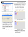
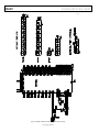
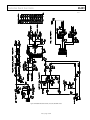
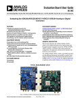
Evaluation Board User Guide
UG-001
One Technology Way • P.O. Box 9106 • Norwood, MA 02062-9106, U.S.A. • Tel: 781.329.4700 • Fax: 781.461.3113 • www.analog.com
Evaluating the AD9272/AD9273 for Ultrasound Systems
FEATURES
DOCUMENTS NEEDED
Full featured evaluation board for the AD9272/AD9273
SPI and alternate clock options
Internal and external reference options
VisualAnalog and SPI Controller software interfaces
AD9272 and AD9273 data sheets
HSC-ADC-EVALCZ data sheet, High Speed Converter
Evaluation Platform (FPGA-based data capture kit)
AN-905 Application Note, VisualAnalog Converter Evaluation
Tool Version 1.0 User Manual
AN-878 Application Note, High Speed ADC SPI Control Software
AN-877 Application Note, Interface to High Speed ADCs via SPI
EQUIPMENT NEEDED
Analog signal source and antialiasing filter
2 switching power supplies (6.0 V, 2.5 A) CUI EPS060250UHPHP-SZ, provided
Linear bench top dc voltage source (0 V to 1.6 V), not
required for CW Doppler mode
PC running Windows 98 (2nd ed.), Windows 2000, Windows ME,
or Windows XP
USB 2.0 port, recommended (USB 1.1 compatible)
AD9272/AD9273 evaluation board
HSC-ADC-EVALCZ FPGA-based data capture kit
For CW Doppler mode: spectrum analyzer
For CW Doppler mode: dc voltage source: +5 V w/100 mA each
SOFTWARE NEEDED
VisualAnalog
SPI Controller
GENERAL DESCRIPTION
This document describes the AD9272/AD9273 evaluation
board, which provides all of the support circuitry required to
operate the AD9272/AD9273 in their various modes and
configurations. The application software used to interface with
the devices is also described.
The AD9272/AD9273 data sheet, available at www.analog.com,
provides additional information and should be consulted when
using the evaluation board. All documents and software tools
are available at http://www.analog.com/fifo. For any questions,
send an email to [email protected].
07782-001
TYPICAL MEASUREMENT SETUP
Figure 1. AD9272-65EBZ/AD9272-80KITZ/AD9273-50EBZ Evaluation Board and HSC-ADC-EVALCZ Data Capture Board
Please see the last page for an important warning and disclaimers.
Rev. 0 | Page 1 of 24
UG-001
Evaluation Board User Guide
TABLE OF CONTENTS
Features .............................................................................................. 1 Default Operation and Jumper Selection Settings ....................5 Equipment Needed ........................................................................... 1 Evaluation Board Software Quick Start Procedures .....................7 Documents Needed .......................................................................... 1 Configuring the Board .................................................................7 Software Needed ............................................................................... 1 Using the Software for Testing.....................................................7 General Description ......................................................................... 1 Typical Measurement Setup ............................................................ 1 Using the Integrated Crosspoint Switch
(CW Doppler Mode) ................................................................. 10 Revision History ............................................................................... 2 Evaluation Board Schematics and Artwork ................................ 12 Evaluation Board Hardware ............................................................ 3 Ordering Information .................................................................... 23 Power Supplies .............................................................................. 3 Bill of Materials ........................................................................... 23 Input Signals .................................................................................. 3 ESD Caution .................................................................................... 24 Output Signals............................................................................... 3 REVISION HISTORY
2/09—Revision 0: Initial Version
Rev. 0 | Page 2 of 24
Evaluation Board User Guide
UG-001
EVALUATION BOARD HARDWARE
The AD9272/AD9273 evaluation board provides all of the support
circuitry required to operate the AD9272/AD9273 in its various
modes and configurations. Figure 2 shows the typical bench
characterization setup used to evaluate the ac performance of
the AD9272/AD9273. It is critical that the signal sources used for
the analog input and clock have very low phase noise (<1 ps rms
jitter) to realize the optimum performance of the signal chain.
Proper filtering of the analog input signal to remove harmonics
and lower the integrated or broadband noise at the input is
necessary to achieve the specified noise performance (see the
AD9272 or AD9273 data sheet).
evaluation board using the SPI and alternate clock options, a
separate 3.3 V analog supply is needed in addition to the other
supplies. The 3.3 V supply, or AVDD_3P3V, should have a 1 A
current capability.
See the Evaluation Board Software Quick Start Procedures section
to get started and Figure 21 to Figure 31 for the complete schematics and layout diagrams that demonstrate the routing and
grounding techniques that should be applied at the system level.
When connecting the clock and analog source, use clean signal
generators with low phase noise, such as Rohde & Schwarz SMA or
HP8644B signal generators or the equivalent. Use a 1 m, shielded,
RG-58, 50 Ω coaxial cable for making connections to the evaluation board. Enter the desired frequency and amplitude (refer to
the specifications in the AD9272 or AD9273 data sheet). The
evaluation board is set up to be clocked from the crystal oscillator, OSC401.
POWER SUPPLIES
This evaluation board comes with a wall-mountable switching
power supply that provides a 6 V, 2 A maximum output. Connect
the supply to the rated 100 V ac to 240 V ac wall outlet at 47 Hz
to 63 Hz. The other end is a 2.1 mm inner diameter jack that
connects to the PCB at P701. Once on the PC board, the 6 V
supply is fused and conditioned before connecting to low dropout
linear regulators that supply the proper bias to each of the various
sections on the board.
When operating the evaluation board in a nondefault condition,
L705, L706, L707, and L709 can be removed to disconnect the
switching power supply. This enables the user to bias each section
of the board individually. Use P602 and P603 to connect a different
supply for each section. At least one 1.8 V supply is needed with
a 1 A current capability for AVDD_DUT and DRVDD_DUT;
however, it is recommended that separate supplies be used for
both analog and digital domains. An additional supply is also
required to supply 3.0 V to the device under test, AVDD2_DUT.
This should also have a 1A current capability. To operate the
To bias the crosspoint switch circuitry or CW section and
differential gain drive circuitry, separate +5 V and −5 V supplies
are required at P601. These should each have 1 A current capability.
This section cannot be biased from a 6 V, 2 A wall supply. Separate
supplies are required at P601.
INPUT SIGNALS
If a different or external clock source is desired, follow the
instructions Clock Circuitry section. Typically, most Analog
Devices evaluation boards can accept ~2.8 V p-p or 13 dBm sine
wave input for the clock. When connecting the analog input
source, it is recommended to use a multipole, narrow-band
band-pass filter with 50 Ω terminations. Analog Devices uses
TTE and K&L Microwave, Inc., band-pass filters. The filter
should be connected directly to the evaluation board.
OUTPUT SIGNALS
The default setup uses the FIFO5 high speed, dual-channel
FIFO data capture board (HSC-ADC-EVALCZ). Two of the
eight channels can then be evaluated at the same time. For more
information on channel settings on these boards and their optional
settings, visit www.analog.com/FIFO.
Rev. 0 | Page 3 of 24
UG-001
Evaluation Board User Guide
WALL OUTLET
100V TO 240V AC
47Hz TO 63Hz
SWITCHING
POWER
SUPPLY
SWITCHING
POWER
SUPPLY
6V DC
2A MAX
SIGNAL
SYNTHESIZER
6V DC
2A MAX
ANALOG INPUT
SPECTRUM
ANALYZER
CW OUTPUT
SIGNAL
SYNTHESIZER
OPTIONAL CLOCK SOURCE
GAIN CONTROL INPUT
Figure 2. Evaluation Board Connection
Rev. 0 | Page 4 of 24
07782-070
PC
RUNNING ADC
ANALYZER
OR VISUAL ANALOG
USER SOFTWARE
AGILENT
POWER SUPPLY
Evaluation Board User Guide
UG-001
PDWN
DEFAULT OPERATION AND
JUMPER SELECTION SETTINGS
This section explains the default and optional settings or modes
allowed on the AD9272/AD9273 Rev. A evaluation board.
Power Circuitry
Connect the switching power supply that is supplied in the
evaluation kit between a rated 100 V ac to 240 V ac wall outlet
at 47 Hz to 63 Hz and P701.
Analog Input Front-End Circuit
The evaluation board is set up for a transformer-coupled analog
input with an optimum 50 Ω impedance match of 18 MHz of
bandwidth. For a different bandwidth response, use the
antialiasing filter settings.
VREF
VREF is set to 1.0 V. This causes the ADC to operate with the
internal reference in the 2.0 V p-p full-scale range. A separate
external reference option using the ADR130 is also included on
the evaluation board. Populate R311 with a 0 Ω resistor and remove
C426. Note that ADC full-scale ranges less than 2.0 V p-p are
not supported by the AD9272/AD9273.
RBIAS
RBIAS has a default setting of 10 kΩ (R301) to ground and is used
to set the ADC core bias current. However, note that using other
than a 10 kΩ, 1% resistor for RBIAS may degrade the performance
of the device, depending on the resistor chosen.
Clock Circuitry
To enable the power-down feature, short P303 to the on
position (AVDD) on the PDWN pin.
STBY
To enable the standby feature, short P302 to the on position
(AVDD) on the STBY pin.
GAIN+, GAIN−
To change the VGA attenuation, drive the GAIN+ pin from 0 V
to 1.6 V on J302 using a linear supply and use a single-ended
method to change the VGA gain from 0 dB to 42 dB. U403 is
available for users who wish to drive the gain pins (GAIN±)
differentially. Install R305, R347, and R349 and remove C308,
C309, and R303 to connect the amplifier correctly. Next, apply a
dc voltage source to P601, connecting the +5 V, −5 V, and ground
(0 V) appropriately to bias U403 (AD8138). These benchtop
linear supplies should each have 100 mA of current capability.
If an external source is not available, R337 can be installed to
use the on-board resistive divider for gain adjustment in either
the single-ended or differential case.
Non-SPI Mode
For users who wish to operate the DUT without using SPI,
remove the jumpers on J601. This disconnects the CSB, SCLK,
and SDIO pins from the control bus, allowing the DUT to
operate in its simplest mode. Each of these pins has internal
termination and will float to its respective level. Note that the
device will only work in its default condition.
CWDx+, CWDx−
The default clock input circuitry is derived from a simple transformer-coupled circuit using a high bandwidth
1:1 impedance ratio transformer (T401) that adds a very low
amount of jitter to the clock path. The clock input is 50 Ω
terminated and ac-coupled to handle single-ended sine wave
types of inputs. The transformer converts the single-ended
input to a differential signal that is clipped before entering the
ADC clock inputs.
The evaluation board is already set up to be clocked from the
crystal oscillator, OSC401. This oscillator is a low phase noise
oscillator from Valpey Fisher (VFAC3-BHL-50MHz/VFAC3BHL-65MHz/VFAC3-BHL-80MHz). If a different clock source
is desired, remove R403, set Jumper J401 to disable the oscillator
from running, and connect the external clock source to the
SMA connector, P401.
A differential LVPECL clock driver can also be used to clock the
ADC input using the AD9515 (U401). Populate R406 and R407
with 0 Ω resistors and remove R415 and R416 to disconnect the
default clock path inputs. In addition, populate C405 and C406
with a 0.1 μF capacitor and remove C409 and C410 to disconnect
the default clock path outputs. The AD9515 has many pinstrappable options that are set to a default mode of operation.
Consult the AD9515 data sheet for more information about
these and other options.
To use the CWDx± outputs, first apply a dc voltage source to
P601, connecting the +5 V, −5 V, and ground (0 V) appropriately to
bias U402 (AD812). These benchtop linear supplies should each
have 100 mA of current capability.
To view the CWD2+/CWD2− through CWD5+/CWD5− outputs,
jumper together the appropriate outputs on P606 and P607. All
outputs are summed together on the IOP and ION buses, fed to
a 1:4 impedance ratio transformer, and buffered so that the user
can view the output on a spectrum analyzer. This can be configured
to be viewed in single-ended mode (default) or in differential mode
by using a spectrum analyzer. To set the voltage for the appropriate
number of channels to be summed, change the value of R447
and R448 on the primary transformer (T402).
Upon shipment, the CWD0+/CWD0−, CWD1+/CWD1−,
CWD6+/CWD6−, and CWD7+/CWD7− outputs are properly
biased and ready to use with the AD8339 quad I/Q demodulator
and phase shifter. The AD9272/AD9273 evaluation board simply
snaps into place on the AD8339 evaluation board (AD8339EVALZ). Remove the jumpers connected to P3A and P4A on
the AD8339 evaluation board, and snap the standoffs that are
provided with the AD9272/AD9273 into the AD8339 evaluation
board standoff holes in the center of the board. The standoffs
will automatically lock into place and create a direct connection
Rev. 0 | Page 5 of 24
UG-001
Evaluation Board User Guide
between the AD9272/AD9273 CWDx± outputs and the
AD8339 inputs.
DOUTx+, DOUTx−
If an alternative data capture method to the setup described in
Figure 2 is used, optional receiver terminations, R701 to R710, can
be installed next to the high speed backplane connector.
Rev. 0 | Page 6 of 24
Evaluation Board User Guide
UG-001
EVALUATION BOARD SOFTWARE QUICK START PROCEDURES
This section provides quick start procedures for using the AD9272/
AD9273 either on the evaluation board or in a system level
design. Both the default and optional settings are described.
CONFIGURING THE BOARD
Before using the software for testing, configure the evaluation
board as follows:
Connect the evaluation board to the data capture board as
shown in Figure 1 and Figure 2.
2.
Connect one 6 V, 2.5 A switching power supply (such as
the CUI Inc. EPS060250UH-PHP-SZ supplied) to the
AD9272/AD9273 board.
3.
Connect one 6 V, 2.5 A switching power supply (such as
the CUI EPS060250UH-PHP-SZ supplied) to the HSCADC-EVALCZ board.
07782-021
1.
Figure 3. VisualAnalog, New Canvas Window
2.
5.
On the ADC evaluation board, place jumpers on all four
pin pairs of J601 to connect the SPI bus.
6.
On the ADC evaluation board, ensure that J401 (OSC_EN)
is jumpered to the on setting to use the on-board 50 MHz/
65 MHz/80 MHz Valpey Fisher VFAC3 oscillator.
7.
On the ADC evaluation board, use a clean signal generator
with low phase noise to provide an input signal to the
desired channel. Use a 1 m, shielded, RG-58, 50 Ω coaxial
cable to connect the signal generator. For best results, use a
narrow-band band-pass filter with 50 Ω terminations and
an appropriate center frequency. (Analog Devices uses
TTE, Allen Avionics, and K&L band-pass filters.)
USING THE SOFTWARE FOR TESTING
If a different program is desired, follow Step 3.
Figure 4. VisualAnalog, Default Configuration Message
3.
Setting Up the ADC Data Capture Block
After configuring the board, set up the ADC data capture block
using the following steps:
1.
After the template is selected, a message appears, asking if
the default configuration can be used to program the FPGA
(see Figure 4). Click Yes, and the window closes.
07782-028
Connect the HSC-ADC-EVALCZ board (J6) to the PC
with a USB cable.
Open VisualAnalog™ on a PC. AD9272 or AD9273 should
be listed in the status bar of the New Canvas window.
Select the template that corresponds to the type of testing
to be performed (see Figure 3).
To view different channels or change features to settings
other than the default settings, click the Expand Display
button. This is located on the bottom right corner of the
window, as shown in Figure 5.
This process is described in the AN-905 Application Note,
VisualAnalog Converter Evaluation Tool Version 1.0 User
Manual. After you are finished, click the Collapse Display
button (see Figure 6).
EXPAND DISPLAY BUTTON
Figure 5. VisualAnalog Window Toolbar, Collapsed Display
Rev. 0 | Page 7 of 24
07782-022
4.
UG-001
Evaluation Board User Guide
Setting Up the SPI Controller
COLLAPSE DISPLAY BUTTON
After the ADC data capture board setup is completed, set up the
SPI Controller using the following procedure:
SETTINGS
BUTTON
Open the SPI Controller software by going to the Start
menu or double-clicking the SPI Controller software
desktop icon. If prompted for a configuration file, select
the appropriate one. If not, check the title bar of the
window to determine which configuration is loaded. If
necessary, choose Cfg Open from the File menu and select
the appropriate one. Note that the CHIP ID(1) field should
be filled to indicate whether the correct SPI Controller
configuration file is loaded or not (see Figure 8).
07782-023
1.
Figure 6. VisualAnalog, Main Window
Program the HSC-ADC-EVALCZ board’s FPGA to a setting
other than the default setting as described in Step 3. Then
expand the VisualAnalog display and click the Settings
button in the ADC Data Capture block (see Figure 6). The
ADC Data Capture Settings box opens (see Figure 7).
07782-016
4.
Figure 8. SPI Controller, CHIP ID(1) Box
2.
Click the New DUT button in the SPI Controller.
07782-025
NEW DUT BUTTON
Figure 7. ADC Data Capture Settings Window, Board Settings Tab
Select the Board Settings tab and browse to the appropriate
programming file. If you are using an encode rate <28 MSPS,
select Octal_Low_Speed.bin. If you are using an encode
rate >28 MSPS, select Octal_High_Speed.bin. Next, click
Program; the DONE LED in the HSC-ADC-EVALCZ board
should then turn on. If more than two channels are required
to be displayed, select Octal_High_8-Channel_synchronous
Capture.bin. This canvas allows the user to display all the
channels at once. The drawback is that each FFT display is
only 8k points.
07782-116
5.
Exit the ADC Data Capture Settings box by clicking OK.
Figure 9. SPI Controller, New DUT Button
3.
Rev. 0 | Page 8 of 24
In the Global tab of the SPI Controller, find the CHIP
GRADE(2) box. Use the drop-down box to select the
correct speed grade, if necessary. See the AD9272 or AD9273
data sheet, the AN-878 Application Note, and the AN-877
Application Note for reference.
Evaluation Board User Guide
UG-001
In the ADC A tab of SPI Controller, find the OFFSET(10)
box. Use the drop-down box labeled Offset Adj to perform
an offset correction to the LNA if the LNA power setting
BIAS_CURR_A(12) has been set low. The default value is 32.
Select 33 if the low LNA power setting BIAS_CURR_A(12)
is used.
07782-018
5.
07782-017
Figure 12. SPI Controller, OFFSET(10) Box
Figure 10. SPI Controller, CHIP GRADE(2) Box
07782-217
In the ADCBase 0 tab of the SPI Controller, find the
HIGHPASS(2B) box. Click Manual Tune to calibrate the
antialiasing filter. See the AD9272 or AD9273 data sheet,
the AN-878 Application Note, and the AN-877 Application
Note for reference.
Figure 13. SPI Controller, BIAS_CURR_A(12) Box
Click the Run button in the VisualAnalog toolbar.
RUN BUTTON
Figure 14. VisualAnalog Window Toolbar, Collapsed Display
Figure 11. SPI Controller, HIGHPASS(2B) Box
Rev. 0 | Page 9 of 24
07782-122
6.
07782-117
4.
UG-001
Evaluation Board User Guide
0
Adjusting the Amplitude of the Input Signal
fIN = 3.5MHz @ –1dBFS
LNA = 6×
VGAIN = 1V
FILTER TUNED
HPF = 700kHz
–10
Next, adjust the amplitude of the input signal for each channel
as follows:
–20
1.
–40
–30
AMPLITUDE (dBFS)
Adjust the amplitude of the input signal so that the
fundamental is at the desired level. (Examine the Fund
Power reading in the left panel of the VisualAnalog FFT
window.) If the gain pin voltage is too low, it is not possible
to reach full scale without distortion. Use a higher gain
setting or a lower input level to avoid distortion. This also
depends on the PGA gain setting, which can be 30 dB,
27 dB, 24 dB, or 21dB. See Figure 15 and Figure 16.
–50
–60
–70
–80
–90
–100
07782-119
–110
–120
–130
0
5
10
15
20
25
FREQUENCY (MHz)
Figure 17. Typical FFT, AD9272/AD9273
USING THE INTEGRATED CROSSPOINT SWITCH
(CW DOPPLER MODE)
07782-026
To examine the spectrum of the CW Doppler integrated
crosspoint switch output, use the following procedure:
Complete the steps in the Configuring the Board and
Using the Software for Testing sections to ensure that the
board is set up correctly.
2.
Optionally, remove the voltage source from the gain pin. It
does not affect the CW Doppler output.
3.
Connect the dc voltage source to P601, connecting the
−5 V pin, the 0 V ground pin, and the +5 V pin as shown
in Figure 1. These benchtop linear supplies should each have
100 mA of current capability.
4.
Place jumpers on the top pin pairs of P606 or P607 to
connect CWD2+/CWD2− to CWD5+/CWD5− to the
IOP/ION buses. This directs each of these connections to
the output amplifier for display.
Note that the CWD0±/CWD1±/CWD6±/CWD7± outputs
are configured and biased to interface with the AD8339
evaluation board. The AD9272/AD9273 is specially designed
to snap onto the AD8339 evaluation board to allow the user to
evaluate a larger portion of this common signal chain. For
detailed instructions about enabling this function, send an
email to [email protected].
07782-027
Figure 15. VisualAnalog, Graph Window
1.
Figure 16. VisualAnalog, Formatted FFT Plot
2.
Repeat this procedure for the other seven channels.
3.
Click the disk icon within the Graph window to save the
performance plot. See Figure 17 for an example.
5.
Use a 1 m, shielded, RG-58, 50 Ω coaxial cable to connect
the spectrum analyzer to J402 (labeled AOUT on the
evaluation board).
6.
In the ADCBase 0 tab of the SPI Controller, find the
MODES(8) box. Select the CW Mode option (see Figure 18).
Rev. 0 | Page 10 of 24
UG-001
07782-030
Evaluation Board User Guide
Figure 19. SPI Controller, CROSSPOINT SWITCH(2D) Box
8.
Examine the spectrum analyzer for the CW Doppler output
(see Figure 20 for an example).
0
–10
FREQUENCY = 2.3MHz
CWD1±, DIFFERENTIAL OUTPUT
AMPLITUDE (dBm)
–20
–30
–40
–50
–60
–70
07782-004
–80
–90
–100
07782-029
0
Figure 18. SPI Controller, MODES(8) Box
7.
In the ADC x tab of the SPI Controller, where x is the channel
to which an analog input is applied, find the CROSSPOINT
SWITCH(2D) box. From the Crosspoint Switch Modes
drop-down box, select the cwd2p/n option (see Figure 19).
Rev. 0 | Page 11 of 24
5
10
15
20
25
FREQUENCY (MHz)
Figure 20. Typical Spectrum Analyzer Display of CWD Output
UG-001
Evaluation Board User Guide
EVALUATION BOARD SCHEMATICS AND ARTWORK
07782-005
Figure 21. Evaluation Board Schematic, DUT Analog Input Circuits
Rev. 0 | Page 12 of 24
Evaluation Board User Guide
UG-001
07782-006
Figure 22. Evaluation Board Schematic, DUT Analog Input Circuits (Continued)
Rev. 0 | Page 13 of 24
UG-001
Evaluation Board User Guide
07782-007
Figure 23. Evaluation Board Schematic, DUT, VREF, and Decoupling
Rev. 0 | Page 14 of 24
Evaluation Board User Guide
UG-001
07782-008
Figure 24. Evaluation Board Schematic, Clock, SPI, and Gain Circuits
Rev. 0 | Page 15 of 24
UG-001
Evaluation Board User Guide
07782-009
Figure 25. Evaluation Board Schematic, Power Supply, CW Doppler, Digital Output Interface
Rev. 0 | Page 16 of 24
UG-001
07782-010
Evaluation Board User Guide
Figure 26. Evaluation Board Layout, Top Side
Rev. 0 | Page 17 of 24
Evaluation Board User Guide
07782-011
UG-001
Figure 27. Evaluation Board Layout, Ground Plane (Layer 2)
Rev. 0 | Page 18 of 24
UG-001
07782-012
Evaluation Board User Guide
Figure 28. Evaluation Board Layout, Power Plane (Layer 3)
Rev. 0 | Page 19 of 24
Evaluation Board User Guide
07782-013
UG-001
Figure 29. Evaluation Board Layout, Power Plane (Layer 4)
Rev. 0 | Page 20 of 24
UG-001
07782-014
Evaluation Board User Guide
Figure 30. Evaluation Board Layout, Ground Plane (Layer 5)
Rev. 0 | Page 21 of 24
Evaluation Board User Guide
07782-015
UG-001
Figure 31. Evaluation Board Layout, Bottom Side
Rev. 0 | Page 22 of 24
Evaluation Board User Guide
UG-001
ORDERING INFORMATION
BILL OF MATERIALS
Table 1.
Item
1
Qty
79
2
9
3
4
5
6
7
8
9
6
1
2
1
1
1
8
10
11
12
5
1
1
13
12
14
15
16
17
18
19
20
21
2
3
2
1
1
1
2
8
22
10
23
24
1
11
25
8
26
16
27
28
29
5
6
8
30
13
31
32
33
1
3
1
Reference Designator
C101, C102, C106, C110, C111, C115, C120,
C121, C125, C130, C131, C136, C201,
C202, C206, C210, C211, C215, C220,
C221, C225, C230, C231, C236, C301,
C302, C304, C305, C306, C307, C308,
C309, C401, C402, C403, C404, C409,
C410, C412, C413, C414, C415, C416,
C419, C420, C421, C422, C423, C425,
C502, C504, C601, C602, C706, C708,
C710, C712, C730, C731, C732, C733,
C734, C735, C740, C742, C743, C744,
C745, C749, C750, C751, C752, C753,
C754, C755, C756, C770, C771, C2201
C426, C714, C715, C716, C717, C719,
C720, C721, C722
C501, C503, C705, C707, C709, C711
C704
C801, C802
C803
CR702
D401
D101, D102, D103, D104, D201, D202,
D203, D204
D701, D702, D703, D704, D705
F701
OSC401
J101, J102, J103, J104, J201, J202, J203,
J204, J302, J402, J403 ,P401
P302, P303
J601, P606, P607
P604, P605
J401
P601
P701
P702, P703
L401, L402, L403, L404, L405, L406,
L407, L408
L501, L502, L702, L703, L704, L705,
L706, L707, L708, L709
L701
R425, R427, R429, R431, R433, R435,
R436, R439, R441, R443, R445
R107, R121, R136, R151, R207, R221,
R236, R251
R102, R116, R131, R146, R202, R216,
R231, R246, R403, R405, R415, R416,
R417, R418, R451, R452
R303, R346, R348, R422, R423
R319, R325, R326, R601, R602, R603
R301, R338, R401, R402, R410, R604,
R605, R606
R101, R115, R130, R145, R201, R215, R230,
R245, R302, R404, R411, R455, R458
R335
R340, R341, R343
R342
Description
Capacitor, 0.1 μF, 0402, ceramic, X5R, 10 V
Manufacturer
Panasonic
Part Number
ECJ-0EB1A104K
Capacitor, 1.0 μF, 0603, ceramic, 16 V, X5R
Panasonic
ECJ-BVB1C105M
Capacitor, 10 μF, 0603, ceramic, 6.3 V, 20%, X5R
Capacitor, 10 μF, 6032-28, tantalum, SMT, 16 V, 10%
Capacitor mono ceramic, 1 μF, 0402, X5R
Capacitor ceramic, 100 pF, 0402
LED, 0603, green
Diode Schottky GP LN 30 V, 20 mA SOT-23
Diode Schottky GP LN 20 V SOT-23
Panasonic
Kemet
Murata
Panasonic
Panasonic
Avago
Fairchild
ECJ-1VB0J106M
T491C106K016AT
GRM155B30J105KE18D
ECJ-0EC1H101J
LNJ314G8TRA
HSMS-2812-TR1G
MMBD4148SE
Diode, silicon rectifier, SMBJ, 2 A, 50 V
Polyswitch 1.1 A reset fuse SMD
CLK oscillator, 3.3 V, 50 MHz/65 MHz/80 MHz
Microcommercial
Tyco/Raychem
Valpey Fisher
SMA, end launch, coaxial
Samtec
S2A-TP
NANOSMDC110F-2
VFAC3-BHL-50MHz,
VFAC3-BHL-65MHz,
VFAC3-BHL-80MHz
SMA-J-P-H-ST-EM1
Header, 2-pin, single row, male, 100 mil, straight
Conn-PCB header 8-pin double row
Conn-PCB header, 8-pin, double row
Header, 3-pin, single row, male, 100 mil, straight
Terminal block, 4-pin, straight
Power supply connector
Header
Inductor chip coil, 560 μH, 1210
Samtec
Samtec
Samtec
Samtec
Weiland
Switchcraft
Tyco
Murata
TSW-102-07-G-S
TSW-104-07-G-D
SSW-104-06-G-D
TSW-103-07-G-S
Z5.531.3425.0
RAPC722X
6469169-1
LQH32MN561J23L
Ferrite chip 50 Ω, 3 A 1206
Murata
BLM31PG500SN1L
EMI filter LC block choke coil
Resistor, thick film, SMT 0201, 0 Ω
Murata
Panasonic
BNX016-01
ERJ-1GE0R00C
Resistor, thick film, SMT 0402, 348 Ω, 1/16 W, 1%
Panasonic
ERJ-2RKF3480X
Resistor, thick film, SMT 0402, 0 Ω
Panasonic
ERJ-2GE0R00X
Resistor, thick film, SMT 0402, 100 Ω, 1/16 W, 1%
Resistor, thick film, SMT 0402, 1.00 kΩ, 1/16 W, 1%
Resistor, thick film, SMT 0402, 10 kΩ, 1/16 W, 1%
Panasonic
Panasonic
Panasonic
ERJ-2RKF1000X
ERJ-2RKF1001X
ERJ-2RKF1002X
Resistor, thick film, SMT 0402, 49.9 Ω, 1/16 W, 1%
Panasonic
ERJ-2RKF49R9X
Resistor, thick film, SMT 0402, 8.66 kΩ, 1/16 W, 1%
Resistor, thick film, SMT 0402, 499 Ω, 1/16 W, 1%
Resistor, thick film, SMT 0402, 523 Ω, 1/16 W, 1%
Panasonic
Panasonic
Panasonic
ERJ-2RKF8661X
ERJ-2RKF4990X
ERJ-2RKF5230X
Rev. 0 | Page 23 of 24
UG-001
Evaluation Board User Guide
Item
34
35
36
37
38
39
40
41
42
43
44
45
46
47
48
49
Qty
1
1
1
3
2
6
1
1
1
1
1
1
1
1
1
1
Reference Designator
R344
R345
R414
R420, R421, R716
R447, R448
R453, R454, R801, R802, R803, R804
R446
R336
T401
T402
U601
U602
U302
U401
U402
U701
50
51
52
53
54
2
1
1
1
1
U704, U707
U705
U706
U403
U301
Description
Resistor, thick film, SMT 0402, 33 kΩ, 1/16 W, 1%
Resistor, thick film, SMT 0402, 10.5 kΩ, 1/16 W, 1%
Resistor, thick film, SMT 0402, 4.12 kΩ, 1/16 W, 1%
Resistor, thick film, SMT 0402, 240 Ω, 1/16 W, 5%
Resistor, thick film, SMT 0402, 124 Ω, 1/16 W, 1%
Resistor, thick film, SMT 0402, 750 Ω, 1/16 W, 1%
Resistor, thick film, SMT 0402, 113 Ω, 1/16 W, 1%
potentiometer, 10 kΩ square cermet top
Transformer, RF, 1:1
Transformer, ADTT4-1, CD542
IC, buffer, UHS dual, OD out, SC70-6
IC, buffer, UHS dual, SC70-6
IC, VREF, precision sub–band gap, 3-lead TSOT
IC, clock distribution, 32-lead LFCSP
IC, op amp, current feedback, dual, 8-lead SOIC
IC high ACC. 500 mA anyCAP® low drop 2.5 V
regulator
IC, regulator, high accuracy, 1.8 V, SOT-223
IC, regulator, high accuracy, 3.3 V, SOT-223
IC, regulator, high accuracy, 3.0 V, SOT-223
IC, low distortion diff ADC driver, 8-lead SOIC
IC, octal LNA/VGA/AAF/ADC and crosspoint switch
TQFP-100 (SV-100-3)
Manufacturer
Panasonic
Panasonic
Panasonic
Panasonic
Panasonic
Panasonic
Panasonic
Copal
Minicircuits
Minicircuits
Fairchild
Fairchild
Analog Devices
Analog Devices
Analog Devices
Analog Devices
Part Number
ERJ-2RKF3302X
ERJ-2RKF1052X
ERJ-2RKF4121X
ERJ-2GEJ241X
ERJ-2RKF1240X
ERJ-2RKF7500X
ERJ-2RKF1130X
CT94EW103
ADT1-1WT+
ADTT4-1+
NC7WZ07P6X
NC7WZ16P6X
ADR130BUJZ-R2
AD9515BCPZ
AD812ARZ
ADP3335ACPZ-2.5R7
Analog Devices
Analog Devices
Analog Devices
Analog Devices
Analog Devices
ADP3339AKCZ-1.8-R7
ADP3339AKCZ-3.3-R7
ADP3339AKCZ-3-RL7
AD8138ARZ
AD9273BSVZ-50,
AD9272BSVZ-65,
AD9272BSVZ-80
ESD CAUTION
Evaluation boards are only intended for device evaluation and not for production purposes. Evaluation boards are supplied “as is” and without warranties of any kind, express,
implied, or statutory including, but not limited to, any implied warranty of merchantability or fitness for a particular purpose. No license is granted by implication or otherwise under
any patents or other intellectual property by application or use of evaluation boards. Information furnished by Analog Devices is believed to be accurate and reliable. However, no
responsibility is assumed by Analog Devices for its use, nor for any infringements of patents or other rights of third parties that may result from its use. Analog Devices reserves the
right to change devices or specifications at any time without notice. Trademarks and registered trademarks are the property of their respective owners. Evaluation boards are not
authorized to be used in life support devices or systems.
©2009 Analog Devices, Inc. All rights reserved. Trademarks and
registered trademarks are the property of their respective owners.
UG07782-0-2/09(0)
Rev. 0 | Page 24 of 24