1
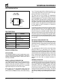
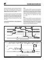
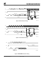
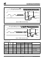
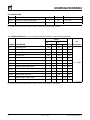
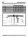
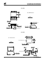
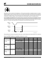
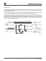
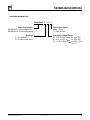
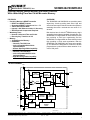
SUMMIT
S93WD462/S93WD463
MICROELECTRONICS, Inc.
Precision Supply-Voltage Monitor and Reset Controller
With a Watchdog Timer and 1k-bit Microwire Memory
FEATURES
• Precision Monitor & RESET Controller
— RESET and RESET Outputs
— Guaranteed RESET Assertion to VCC = 1V
— 150ms Reset Pulse Width
— Internal 1.26V Reference with ±1% Accuracy
— ZERO External Components Required
• Watchdog Timer
— Nominal 1.6 Second Time-out Period
— Reset by Any Transition of CS
• Memory
— 1K-bit Microwire Memory
— S93WD462
– Internally Ties ORG Low
– 100% Compatible With all 8-bit
Implementations
– Sixteen Byte Page Write Capability
— S93WD463
– Internally Ties ORG High
– 100% Compatible With all 16-bit
Implementations
– Eight Word Page Write Capability
OVERVIEW
The S93WD462 and S93WD463 are precision power
supervisory circuits providing both active high and
active low reset output. Both devices also incorporate a
watchdog timer with a nominal time-out value of 1.6
seconds.
Both devices have 1k-bits of E2PROM memory that is
accessible via the industry standard microwire bus. The
S93WD462 is configured with an internal ORG pin tied
low providing a 8-bit byte organization and the
S93WD463 is configured with an internal ORG pin tied
high providing a 16-bit word organization. Both the
S93WD462 and S93WD463 have page write capability. The devices are designed for a minimum 100,000
program/erase cycles and have data retention in excess of 100 years.
BLOCK DIAGRAM
VCC
8
5kHz
OSCILLATOR
+
RESET
PULSE
GENERATOR
VTRIP
SK
2
DI
3
MODE
DECODE
DATA I/O
DO
4
7
RESET
WATCHDOG
TIMER
1.26V
1
RESET#
RESET
CONTROL
–
CS
6
ADDRESS
DECODER
WRITE
CONTROL
E2PROM
MEMORY
ARRAY
5
2029 T BD 2.0
GND
© SUMMIT MICROELECTRONICS, Inc. 2001 • 300 Orchard City Drive, Suite 131 • Campbell, CA 95008 • Telephone 408-378-6461 • Fax 408-378-6586 • www.summitmicro.com
Characteristics subject to change without notice
2029 2.2 1/23/01
1
S93WD462/S93WD463
PIN CONFIGURATION
VTRIP. The reset outputs will be valid so long as VCC is ≥
1.0V. During power-down, the reset outputs will begin
driving active when VCC falls below VTRIP.
8-Pin PDIP
or 8-Pin SOIC
CS
SK
DI
DO
1
2
3
4
8
7
6
5
The reset pins are I/Os; therefore, the S93WD462/
WD463 can act as a signal conditioning circuit for an
externally applied reset. The inputs are edge triggered;
that is, the RESET input will initiate a reset time-out after
detecting a low to high transition and the RESET# input
will initiate a reset time-out after detecting a high to low
transition. Refer to the applications Information section
for more details on device operation as a debounce/
reset extender circuit.
VCC
RESET
RESET#
GND
2029 T PCon 2.0
It should be noted the reset outputs are open drain. When
used as outputs driving a circuit they need to be either
tied high (RESET#) or tied to ground (RESET) through
the use of pull-up or pull-down resistors. Refer to the
applications aid section for help in determining the value
of resistor to be used. Internally these pins are weakly
pulled up (RESET#) and pulled down (RESET): therefore, if the signals are not being used the pins may be left
unconnected.
PIN FUNCTIONS
Pin Name
Function
CS
Chip Select
SK
Clock Input
DI
Serial Data Input
DO
Serial Data Output
VCC
+2.7 to 6.0V Power Supply
GND
Ground
RESET/RESET#
WATCHDOG TIMER DESCRIPTION
The S93WD462/WD463 has a watchdog timer with a
nominal time-out period of 1.6 seconds. Whenever the
watchdog times out, it will generate a reset output to both
pins 6 and 7. The watchdog timer is reset by any
transition on CS.
RESET I/O
DEVICE OPERATION
APPLICATIONS
The S93WD462/WD463 is ideal for applications requiring low voltage and low power consumption. This device
provides microcontroller RESET control and can be
manually resettable.
RESET CONTROLLER DESCRIPTION
The S93WD462/WD463 provides a precision reset controller that ensures correct system operation during
brownout and power-up/-down conditions. It is configured with two open drain reset outputs; pin 7 is an active
high output and pin 6 is an active low output.
During power-up, the reset outputs remain active until
VCC reaches the VTRIP threshold. The outputs will continue to be driven for approximately 150ms after reaching
2
2029
The watchdog timer will be held in a reset state during
power-on while VCC is less than VTRIP. Once VCC
exceeds VTRIP the watchdog will continue to be held in
a reset state for the tPURST period. After tPURST it will be
released and the timer will begin operation. If either reset
input is asserted the watchdog timer will be reset and
remain in the reset condition until either tPURST has
expired or the reset input is released, whichever is
longer.
GENERAL OPERATION
The S93WD462/WD463 is a 1024-bit nonvolatile memory
intended for use with industry standard microprocessors. The S93WD463 is organized as X16, seven 9-bit
instructions control the reading, writing and erase
operations of the device. The S93WD462 is organized
as X8, seven 10-bit instructions control the reading,
writing and erase operations of the device. The device
operates on a single 3V or 5V supply and will generate on
chip, the high voltage required during any write operation.
2.2 1/23/01
SUMMIT MICROELECTRONICS, Inc.
S93WD462/S93WD463
Instructions, addresses, and write data are clocked into
the DI pin on the rising edge of the clock (SK). The DO
pin is normally in a high impedance state except when
reading data from the device, or when checking the
ready/busy status after a write operation.
Read
Upon receiving a READ command and an address
(clocked into the DI pin), the DO pin of the S93WD462/
WD463 will come out of the high impedance state and,
will first output an initial dummy zero bit, then begin
shifting out the data addressed (MSB first). The output
data bits will toggle on the rising edge of the SK clock and
are stable after the specified time delay
(tPD0 or tPD1).
The ready/busy status can be determined after the start
of a write operation by selecting the device (CS high)
and polling the DO pin; DO low indicates that the write
operation is not completed, while DO high indicates that
the device is ready for the next instruction. See the
Applications Aid section for detailed use of the ready
busy status.
Write
After receiving a WRITE command, address and the
data, the CS (Chip Select) pin must be deselected for a
minimum of 250ns (tCSMIN). The falling edge of CS will
start automatic erase and write cycle to the memory
location specified in the instruction. The ready/busy
status of the S93WD462/WD463 can be determined by
selecting the device and polling the DO pin.
The format for all instructions is: one start bit; two op
code bits and either six (x16) or seven (x8) address or
instruction bits.
t SKLOW
tSKHI
t CSH
SK
t DIS
t DIH
VALID
DI
VALID
t CSS
CS
t DIS
t PD0,t PD1
DO
tCSMIN
DATA V ALID
2029 ILL 3.0
Figure 1. Sychronous Data Timing
SK
tCS
CS
STANDBY
AN
DI
1
1
DO
AN–1
A0
0
HIGH-Z
tHZ
tPD0
HIGH-Z
0
DN
DN–1
D1
D0
2029 ILL4.0
Figure 2. Read Instruction Timing
SUMMIT MICROELECTRONICS, Inc.
2029
2.2 1/23/01
3
S93WD462/S93WD463
Erase
Upon receiving an ERASE command and address, the
CS (Chip Select) pin must be deselected for a minimum
of 250ns (tCSMIN). The falling edge of CS will start the
auto erase cycle of the selected memory location. The
ready/busy status of the S93WD462/WD463 can be
determined by selecting the device and polling the DO
pin. Once cleared, the content of a cleared location
returns to a logical “1” state.
Erase/Write Enable and Disable
The S93WD462/WD463 powers up in the write disable
state. Any writing after power-up or after an EWDS
(write disable) instruction must first be preceded by the
EWEN (write enable) instruction. Once the write instruction is enabled, it will remain enabled until power to
the device is removed, or the EWDS instruction is sent.
The EWDS instruction can be used to disable all
S93WD462/WD463 write and clear instructions, and
will prevent any accidental writing or clearing of the
device. Data can be read normally from the device
regardless of the write enable/disable status.
Page Write
93WD462 - Assume WEN has been issued. The host
will then take CS high, and begin clocking in the start
bit, write command and 7-bit address immediately
followed by the first byte of data to be written. The host
can then continue clocking in 8-bit bytes of data with
each byte to be written to the next higher address.
Internally the address pointer is incremented after
receiving each group of eight clocks; however, once
the address counter reaches xxx 1111 it will roll over
to xxx 0000 with the next clock. After the last bit is
clocked in no internal write operation will occur until CS
is brought low.
93WD463 - Assume WEN has been issued. The host
will then take CS high, and begin clocking in the start
bit, write command and 6-bit address immediately
followed by the first 16-bit word of data to be written.
The host can then continue clocking in 16-bit words of
data with each word to be written to the next higher
4
2029
Erase All
Upon receiving an ERAL command, the CS (Chip Select) pin must be deselected for a minimum of 250ns
(tCSMIN). The falling edge of CS will start the self clocking
clear cycle of all memory locations in the device. The
clocking of the SK pin is not necessary after the device
has entered the self clocking mode. The ready/busy
status of the S93WD462/WD463 can be determined by
selecting the device and polling the DO pin. Once
cleared, the contents of all memory bits will be in a
logical “1” state.
Write All
Upon receiving a WRAL command and data, the CS
(Chip Select) pin must be deselected for a minimum of
250ns (tCSMIN). The falling edge of CS will start the self
clocking data write to all memory locations in the device.
The clocking of the SK pin is not necessary after the
device has entered the self clocking mode. The ready/
busy status of the S93WD462/WD463 can be determined by selecting the device and polling the DO pin. It
is not necessary for all memory locations to be cleared
before the WRAL command is executed.
address. Internally the address pointer is incremented
after receiving each group of sixteen clocks; however,
once the address counter reaches xxx x111 it will roll
over to xx x000 with the next clock. After the last bit is
clocked in no internal write operation will occur until CS
is brought low.
Continuous Read
This begins just like a standard read with the host
issuing a read instruction and clocking out the data
byte [word]. If the host then keeps CS high and
continues generating clocks on SK, the S93WD462/
WD463 will output data from the next higher address
location. The S93WD462/WD463 will continue
incrementing the address and outputting data so long
as CS stays high. If the highest address is reached, the
address counter will roll over to address 0000. CS
going low will reset the instruction register and any
subsequent read must be initiated in the normal manner of issuing the command and address.
2.2 1/23/01
SUMMIT MICROELECTRONICS, Inc.
S93WD462/S93WD463
SK
tCS
CS
STANDBY
STATUS
VERIFY
AN
1
DI
0
AN-1
A0
DN
D0
1
tSV
BUSY
HIGH-Z
DO
tHZ
READY
HIGH-Z
tEW
2029 ILL 5.0
Figure 3. Write Instruction Timing
SK
STATUS VERIFY
CS
AN
1
DI
1
tCS
A0
AN-1
STANDBY
1
tSV
tHZ
HIGH-Z
DO
BUSY
READY
HIGH-Z
tEW
2029 ILL6.0
Figure 4. Erase Instruction Timing
SK
STANDBY
CS
DI
1
0
0
*
* ENABLE = 11
DISABLE = 00
2029 Fig05
Figure 5. EWEN/EWDS Instruction Timing
SUMMIT MICROELECTRONICS, Inc.
2029
2.2 1/23/01
5
S93WD462/S93WD463
SK
CS
STANDBY
STATUS VERIFY
t CS
DI
1
0
0
0
1
t SV
t HZ
HIGH-Z
DO
BUSY
READY
HIGH-Z
t EW
2029 ILL 8.0
Figure 6. ERAL Instruction Timing
SK
CS
STATUS VERIFY
STANDBY
t CS
DI
1
0
0
0
DN
1
DO
t SV
t HZ
DO
BUSY
READY
HIGH-Z
t EW
2029 ILL 10.0
Figure 7. WRAL Instruction Timing
INSTRUCTION SET
Instruction
Start
Bit
Opcode
Address
x8
x16
Data
x8
Comments
READ
1
10
A6–A0
A5–A0
ERASE
1
11
A6–A0
A5–A0
WRITE
1
01
A6–A0
A5–A0
EWEN
1
00
11xxxxx
11xxxx
Write Enable
EWDS
1
00
00xxxxx
00xxxx
Write Disable
ERAL
1
00
10xxxxx
10xxxx
Clear All Addresses
WRAL
1
00
01xxxxx
01xxxx
x16
Read Address AN–A0
Clear Address AN–A0
D7–D0
D7–D0
D15–D0
D15–D0
Write Address AN–A0
Write All Addresses
2029 PGM T5.0
6
2029
2.2 1/23/01
SUMMIT MICROELECTRONICS, Inc.
S93WD462/S93WD463
ABSOLUTE MAXIMUM RATINGS*
Temperature Under Bias .................................................................................................................................... –55°C to +125°C
Storage Temperature ......................................................................................................................................... –65°C to +150°C
Voltage on any Pin with Respect to Ground(1) ............................................................................................. –2.0V to +VCC +2.0V
VCC with Respect to Ground .................................................................................................................................. –2.0V to +7.0V
Package Power Dissipation Capability (Ta = 25°C) ............................................................................................................. 1.0W
Lead Soldering Temperature (10 secs) .............................................................................................................................. 300°C
Output Short Circuit Current(2) ........................................................................................................................................... 100 mA
*COMMENT
Stresses above those listed under “Absolute Maximum Ratings” may cause permanent damage to the device. These are stress ratings only, and functional
operation of the device at these or any other conditions outside of those listed in the operational sections of this specification is not implied. Exposure to
any absolute maximum rating for extended periods may affect device performance and reliability.
RECOMMENDED OPERATING CONDITIONS
Temperature
Commercial
Min
0°C
Max
+70°C
Industrial
-40°C
+85°C
2029 PGM T7.0
RELIABILITY CHARACTERISTICS
Symbol
Parameter
Min.
Max.
Units
Reference Test Method
100,000
Cycles/Byte
MIL-STD-883, Test Method 1033
NEND(3)
Endurance
TDR(3)
Data Retention
100
Years
MIL-STD-883, Test Method 1008
VZAP(3)
ESD Susceptibility
2000
Volts
MIL-STD-883, Test Method 3015
ILTH(3)(4)
Latch-Up
100
mA
JEDEC Standard 17
2029 PGM T2.1
D.C. OPERATING CHARACTERISTICS (over recommended operating conditions unless otherwise specified)
Limits
Symbol
Parameter
Min.
Typ.
Max.
Units
Test Conditions
ICC
Power Supply Current
(Operating)
3
mA
DI = 0.0V, fSK = 1MHz
VCC = 5.0V, CS = 5.0V,
Output Open
ISB
Power Supply Current
(Standby)
50
µA
CS = 0V
Reset Outputs Open
ILI
Input Leakage Current
2
µA
VIN = 0V to VCC
ILO
Output Leakage Current
(Including ORG pin)
10
µA
VOUT = 0V to VCC,
CS = 0V
VIL1
VIH1
Input Low Voltage
Input High Voltage
-0.1
2
0.8
VCC+1
V
V
4.5V-VCC<5.5V
VIL2
VIH2
Input Low Voltage
Input High Voltage
0
VCCX0.7
VCCX0.2
VCC+1
V
V
1.8V-VCC<2.7V
VOL1
VOH1
Output Low Voltage
Output High Voltage
0.4
2.4
V
V
4.5V-VCC<5.5V
IOL = 2.1mA
IOH = -400µA
VOL2
VOH2
Output Low Voltage
Output High Voltage
0.2
VCC-0.2
V
V
1.8V-VCC<2.7V
IOL = 1mA
IOH = -100µA
2029 PGM T3.0
Note:
(1) The minimum DC input voltage is –0.5V. During transitions, inputs may undershoot to –2.0V for periods of less than 20 ns. Maximum DC
voltage on output pins is VCC +0.5V, which may overshoot to VCC +2.0V for periods of less than 20 ns.
(2) Output shorted for no more than one second. No more than one output shorted at a time.
(3) This parameter is tested initially and after a design or process change that affects the parameter.
(4) Latch-up protection is provided for stresses up to 100 mA on address and data pins from –1V to VCC +1V.
SUMMIT MICROELECTRONICS, Inc.
2029
2.2 1/23/01
7
S93WD462/S93WD463
PIN CAPACITANCE
Symbol
(1)
COUT
CIN(1)
Test
Max.
Units
Conditions
OUTPUT CAPACITANCE (DO)
5
pF
VOUT=OV
INPUT CAPACITANCE (CS, SK, DI, ORG)
5
pF
VIN=OV
Note:
(1) This parameter is tested initially and after a design or process change that affects the parameter.
2029 PGM T4.0
A.C. CHARACTERISTICS (over recommended operating conditions unless otherwise specified)
Limits
VCC=2.7V-4.5V VCC=4.5V-5.5V
Max.
Min.
Test
SYMBOL PARAMETER
Min.
tCSS
CS Setup Time
100
50
ns
tCSH
CS Hold Time
0
0
ns
VIL = 0.45V
tDIS
DI Setup Time
200
100
ns
VIH = 2.4V
tDIH
DI Hold Time
200
100
ns
CL = 100pF
tPD1
Output Delay to 1
0.5
0.25
µs
VOL = 0.8V
tPD0
Output Delay to 0
0.5
0.25
µs
tHZ(1)
Output Delay to High-Z
200
100
ns
VOH = 2.0v
CL = 100pF
tEW
Program/Erase Pulse Width
10
10
ms
tCSMIN
Minimum CS Low Time
0.5
0.25
µs
tSKHI
Minimum SK High Time
0.5
0.25
µs
tSKLOW
Minimum SK Low Time
0.5
0.25
µs
tSV
Output Delay to Status Valid
SKMAX
Maximum Clock Frequency
0.5
DC
500
DC
Note:
(1) This parameter is tested initially and after a design or process change that affects the parameter.
8
2029
2.2 1/23/01
Max. UNITS Conditions
0.25
µs
1000
KHZ
CL = 100pF
2029 PGM T6.0
SUMMIT MICROELECTRONICS, Inc.
S93WD462/S93WD463
RESET CIRCUIT AC and DC ELECTRICAL CHARACTERISTICS
2.7
Symbol
Parameter
5 Volt-A
5 Volt-B
Min
Max
Min
Max
Min
Max
Unit
VTRIP
Reset Trip Point
2.55
2.7
4.25
4.5
4.50
4.75
V
tPURST
Power-Up Reset Timeout
130
270
130
270
130
270
ms
tRPD
VTRIP to RESET Output Delay
5
µs
VRVALID
RESET# Output Valid
tGLITCH
Glitch Reject Pulse Width
30
30
30
ns
VOLRS
RESET# Output Low Voltage IOL=1mA
0.4
0.4
0.4
V
VOHRS
RESET Output High IOH
5
1
5
1
VCC-.75
VCC-.75
1
V
VCC-.75
V
2029 PGM T1.0
tGLITCH
VTRIP
VRVALID
VCC
tRPD
tPURST
tPURST
RESET#
tRPD
RESET
2029 T fig08 2.0
Figure 8. RESET Timing Diagram
SUMMIT MICROELECTRONICS, Inc.
2029
2.2 1/23/01
9
S93WD462/S93WD463
8 Pin SOIC
Ref. JEDEC MS-012
0.150 - 0.157
(3.80 - 4.00)
1
Inches
(Millimeters)
0.189 - 0.196
(4.80 - 5.00)
0.053 - 0.069
(1.35 - 1.75)
0.013 - 0.020
(0.33 - 0.51)
0.010 - 0.020
×45º
(0.25 - 0.50)
0.004 - 0.010
(0.10 - 0.25)
0.016 - 0.050
(0.40 - 1.27)
.05 (1.27) TYP.
0.228 - 0.244
(5.80 - 6.20)
8 Pin SOIC
8 Pin PDIP
0.355 - 0.400
(9.02 - 10.2)
Ref. JEDEC MS-001
0.24 - 0.28
(6.1 - 7.1)
PIN 1 INDICATOR
Inches
(Millimeters)
0.045 - 0.070
(1.14 - 1.78)
0.300 - 0.325
(7.62 - 8.25)
0.21
MAX.
(5.33)
SEATING PLANE
0.43
MAX.
(10.9)
0.008 - 0.014
(0.20 - 0.36)
0.014 - 0.022
(0.36 - 0.56)
0.115 - 0.195
(2.92 - 4.95)
.015
Min.
(.381)
1
.100
(2.54)
0.115 - 0.195
(2.92 - 4.95)
8 Pin PDIP
10
2029
2.2 1/23/01
SUMMIT MICROELECTRONICS, Inc.
S93WD462/S93WD463
Frequently the reset controller will be deployed on a PC board that provides a peripheral function to a system.
Examples might be modem or network cards in a PC or a PCMCIA card in a laptop. In instances like this the peripheral
card may have a requirement for a clean reset function to insure proper operation. The system may or may not provide
a reset pulse of sufficient duration to clear the peripheral or to protect data stored in a nonvolatile memory.
The I/O capability of the RESET pins can provide a solution. The system’s reset signal to the peripheral can be fed
into the S93WD462/WD463 and it in turn can clean up the signal and provide a known entity to the peripheral’s circuits.
The figure below shows the basic timing characteristics under the assumption the reset input is shorter in duration
than tPURST. The same reset output affect can be attained by using the active high reset input.
RESET#
Input
RESET#
Output
RESET
Output
t PURST
2029 T fig09 2.0
When planning your resistor pull-up and pull-down values, use the following chart to help determine min. resistances.
Worst Case RESET Sink/Source Capabilities at Various VCC Levels
Parameter
Symbol
RESET# Output
VOL
Voltage
RESET# Output
VOL
Voltage
RESET Output
VOH
Voltage
Condition
Min
Typ
Max
Units
VCC = 1.0V, IOL=100µA
0.3
V
VCC = 1.2V, IOL=100µA
0.3
V
VCC = 3.0V, IOL=500µA
0.3
V
VCC = 3.6V, IOL=500µA
0.3
V
VCC = 4.5V, IOL=750µA
0.3
V
VCC = 1.0V, IOL=100µA
0.4
V
VCC = 1.2V, IOL=150µA
0.4
V
VCC = 3.0V, IOL=750µA
0.4
V
VCC = 3.6V, IOL=1mA
0.4
V
VCC = 4.5V, IOL=1mA
0.4
V
VCC = 1.0V, IOH=400µA
VCC-0.75
V
VCC = 1.2V, IOH=800µA
VCC-0.75
V
VCC = 3.0V, IOH=800µA
VCC-0.5
V
VCC = 3.6V, IOH=800µA
VCC-0.5
V
VCC = 4.5V, IOH=800µA
VCC-0.5
V
2029 PGM T5.0
SUMMIT MICROELECTRONICS, Inc.
2029
2.2 1/23/01
11
S93WD462/S93WD463
Ready/Busy Status
During the internal write operation the S93WD462/WD463 memory array is inaccessible. After starting the write
operation (taking CS low) the host can implement a 10ms timeout routine or alternatively it can employ a polling routine
that tests the state of the DO pin.
After starting the write, testing for the status is easily accomplished by taking CS high and testing the state of DO. If
it is low the device is still busy with the internal write. If it is high the write operation has completed.
For the polling routine the host has the option of toggling CS for each test of DO, or it can place CS high and then
intermittently test DO. SK is not required for any of these operations. Once the device is ready, it will continue to drive
DO high whenever the S93WD462/WD463 is selected. The ready state of DO can be cleared by clocking in a start
bit; this start bit can either be the beginning of a new command sequence or it can be a dummy start bit with CS returning
low before the host issues a new command.
SK
CS
STATUS VERIFY
t CS
DI
t SV
t HZ
DO
BUSY
HIGH-Z
READY
HIGH-Z
t EW
STATUS CLEARED
2029 ILL 13.0
12
2029
2.2 1/23/01
SUMMIT MICROELECTRONICS, Inc.
S93WD462/S93WD463
ORDERING INFORMATION
S93WD462
P
A
T
Tape & Reel Option
Blank = Tube
T = Tape & Reel
Base Part Number
S93WD462 = 8-bit configuration
S93WD463 = 16-bit configuration
Package
P = 8 lead PDIP
S = 8 lead 150mil SOIC
Operating Voltage Range
A = 4.5V to 5.5V VTRIP min. @ 4.25V
B = 4.5V to 5.5V VTRIP min. @ 4.50V
2.7 = 2.7V to 5.5V VTRIP min. @ 2.55V
2029 Tree 2.0
SUMMIT MICROELECTRONICS, Inc.
2029
2.2 1/23/01
13
S93WD462/S93WD463
NOTICE
SUMMIT Microelectronics, Inc. reserves the right to make changes to the products contained in this publication in
order to improve design, performance or reliability. SUMMIT Microelectronics, Inc. assumes no responsibility for
the use of any circuits described herein, conveys no license under any patent or other right, and makes no
representation that the circuits are free of patent infringement. Charts and schedules contained herein reflect
representative operating parameters, and may vary depending upon a user’s specific application. While the
information in this publication has been carefully checked, SUMMIT Microelectronics, Inc. shall not be liable for any
damages arising as a result of any error or omission.
SUMMIT Microelectronics, Inc. does not recommend the use of any of its products in life support or aviation
applications where the failure or malfunction of the product can reasonably be expected to cause any failure of either
system or to significantly affect their safety or effectiveness. Products are not authorized for use in such applications
unless SUMMIT Microelectronics, Inc. receives written assurances, to its satisfaction, that: (a) the risk of injury or
damage has been minimized; (b) the user assumes all such risks; and (c) potential liability of SUMMIT
Microelectronics, Inc. is adequately protected under the circumstances.
© Copyright 2001 SUMMIT Microelectronics, Inc.
This Document supersedes all previous versions..
14
2029
2.2 1/23/01
SUMMIT MICROELECTRONICS, Inc.