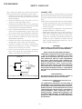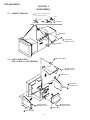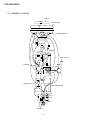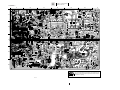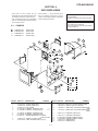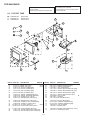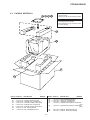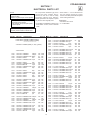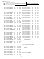
1
CPD-E400/E400E SERVICE MANUAL CPD-E400 US Model Canadian Model Chassis No. SCC-L30K-A CPD-E400E AEP Model Chassis No. SCC-L30K-A F99 CHASSIS SPECIFICATIONS CRT Viewable image size 0.24 mm aperture grille pitch (center) 19 inches measured diagonally 90-degree deflection FD Trinitron Approx. 365 × 274 mm (w/h) (14 3/8 × 10 7/8 inches) 18.0" viewing image Resolution Maximum Horizontal: 1800 dots Vertical: 1440 lines Recommended Horizontal: 1280 dots Vertical: 1024 lines Standard image area Approx. 352 × 264 mm (w/h) (13 7/8 × 10 1/2 inches) Deflection frequency* Horizontal: 30 to 96 kHz Vertical: 48 to 120 Hz AC input voltage/current Power consumption Operating temperature Dimensions Mass Plug and Play 100 to 240 V, 50 – 60 Hz, Max. 2.0 A 140 W 10˚C to 40˚C Approx. 446 × 464 × 461 mm (w/h/d) (17 5/8 × 18 3/8 × 18 1/4 inches) Approx. 26 kg (57 lb 5 oz) DDC1/DDC2B/DDC2Bi/GTF * Recommended horizontal and vertical timing condition • Horizontal sync width should be more than 1.0 µsec. • Horizontal blanking width should be more than 3.0 µsec. • Vertical blanking width should be more than 500 µsec. Design and specifications are subject to change without notice. TRINITRON COLOR COMPUTER DISPLAY ® CPD-E400/E400E SAFETY CHECK-OUT After correcting the original service problem, perform the following safety checks before releasing the set to the customer: 1. Check the area of your repair for unsoldered or poorly-soldered connections. Check the entire board surface for solder splashes and bridges. 2. Check the interboard wiring to ensure that no wires are “pinched” or contact high-wattage resistors. 3. Check that all control knobs, shields, covers, ground straps, and mounting hardware have been replaced. Be absolutely certain that you have replaced all the insulators. 4. Look for unauthorized replacement parts, particularly transistors, that were installed during a previous repair. Point them out to the customer and recommend their replacement. 5. Look for parts which, though functioning, show obvious signs of deterioration. Point them out to the customer and recommend their replacement. 6. Check the line cords for cracks and abrasion. Recommend the replacement of any such line cord to the customer. 7. Check the B+ and HV to see if they are specified values. Make sure your instruments are accurate; be suspicious of your HV meter if sets always have low HV. 8. Check the antenna terminals, metal trim, “metallized” knobs, screws, and all other exposed metal parts for AC Leakage. Check leakage as described below. To Exposed Metal Parts on Set 0.15 µF 1.5 k Ω AC Voltmeter (0.75 V) Earth Ground Fig. A. Using an AC voltmeter to check AC leakage. LEAKAGE TEST The AC leakage from any exposed metal part to earth ground and from all exposed metal parts to any exposed metal part having a return to chassis, must not exceed 0.5 mA (500 microamperes). Leakage current can be measured by any one of three methods. 1. A commercial leakage tester, such as the Simpson 229 or RCA WT-540A. Follow the manufacturers’ instructions to use these instruments. 2. A battery-operated AC milliammeter. The Data Precision 245 digital multimeter is suitable for this job. 3. Measuring the voltage drop across a resistor by means of a VOM or battery-operated AC voltmeter. The “limit” indication is 0.75 V, so analog meters must have an accurate lowvoltage scale. The Simpson 250 and Sanwa SH-63Trd are examples of a passive VOMs that are suitable. Nearly all battery operated digital multimeters that have a 2 V AC range are suitable. (See Fig. A) WARNING!! NEVER TURN ON THE POWER IN A CONDITION IN WHICH THE DEGAUSS COIL HAS BEEN REMOVED. SAFETY-RELATED COMPONENT WARNING!! COMPONENTS IDENTIFIED BY SHADING AND MARK ¡ ON THE SCHEMATIC DIAGRAMS, EXPLODED VIEWS AND IN THE PARTS LIST ARE CRITICAL FOR SAFE OPERATION. REPLACE THESE COMPONENTS WITH SONY PARTS WHOSE PART NUMBERS APPEAR AS SHOWN IN THIS MANUAL OR IN SUPPLEMENTS PUBLISHED BY SONY. CIRCUIT ADJUSTMENTS THAT ARE CRITICAL FOR SAFE OPERATION ARE IDENTIFIED IN THIS MANUAL. FOLLOW THESE PROCEDURES WHENEVER CRITICAL COMPONENTS ARE REPLACED OR IMPROPER OPERATION IS SUSPECTED. AVERTISSEMENT!! NE JAMAIS METTRE SOUS TENSION QUAND LA BOBINE DE DEMAGNETISATION EST ENLEVÉE. ATTENTION AUX COMPOSANTS RELATIFS À LA SÉCURITÉ!! LES COMPOSANTS IDENTIFIÉS PAR UNE TRAME ET UNE MARQUE ¡ SONT CRITIQUES POUR LA SÉCURITÉ. NE LES REMPLACER QUE PAR UNE PIÈCE PORTANT LE NUMÉRO SPECIFIÉ. LES RÉGLAGES DE CIRCUIT DONT L’IMPORTANCE EST CRITIQUE POUR LA SÉCURITÉ DU FONCTIONNEMENT SONT IDENTIFIÉS DANS LE PRÉSENT MANUEL. SUIVRE CES PROCÉDURES LORS DE CHAQUE REMPLACEMENT DE COMPOSANTS CRITIQUES, OU LORSQU’UN MAUVAIS FONCTIONNE-MENT EST SUSPECTÉ. –2– CPD-E400/E400E POWER SAVING FUNCTION This monitor meets the power-saving guidelines set by VESA, ENERGY STAR, and NUTEK. If the monitor is connected to a computer or video graphics board that is DPMS (Display Power Management Signaling) compliant, the monitor will automatically reduce power consumption in three stages as shown below. Power mode Power consumption 1 (power) indicator normal operation ≤ 140 W green 1 standby ≤ 15 W green and orange alternate 2 suspend (sleep)* ≤ 15 W green and orange alternate 3 active off** (deep sleep)* ≤3W orange power off 0W off * “Sleep” and “deep sleep” are power saving modes defined by the Environmental Protection Agency. ** When your computer is in a power saving mode, MONITOR IS IN POWER SAVE MODE appears on the screen if you press any button on the monitor. After a few seconds, the monitor enters the power saving mode again. DIAGNOSIS This monitor is equipped with a self-diagnosis function. If there is a problem with your monitor or computer, the screen will go blank and the 1 (power) indicator will either light up green or flash orange. If the 1 (power) indicator is lit in orange, the computer is in power saving mode. Try pressing any key on the keyboard. If all four color bars appear (white, red, green, blue), the monitor is working properly. Reconnect the video input cable and check the condition of your computer. If the color bars do not appear, there is a potential monitor failure. Inform your authorized Sony dealer of the monitor’s condition. MENU RESET If the 1 (power) indicator is flashing orange Press the 1 (power) button twice to turn the monitor off and then on. If the 1 (power) indicator lights up green, the monitor is working properly. 1 (power) indicator If the 1 (power) indicator is green If the 1 (power) indicator is still flashing, there is a potential monitor failure. Count the number of seconds between orange flashes of the 1 (power) indicator and inform your authorized Sony dealer of the monitor’s condition. Be sure to note the model name and serial number of your monitor. Also note the make and model of your computer and video board. 1 Disconnect the video input cable or turn off the connected computer. 2 Press the 1 (power) button twice to turn the monitor off and then on. 3 Move the control button , for 2 seconds before the monitor enters power saving mode. MENU –3– CPD-E400/E400E TIMING SPECIFICATION MODE AT PRODUCTION RESOLUTION CLOCK MODE 1 MODE 2 738 X 414 1600 X 1200 28.322 MHz 202.500 MHz 31.469 kHz 93.750 kHz HORIZONTAL H-FREQ usec usec H. TOTAL 31.777 10.667 H. BLK 5.720 2.765 H. FP 0.318 0.316 H. SYNC 3.813 0.948 H. BP 1.589 1.501 H. ACTIV 26.057 7.901 70.087 Hz 75.000 Hz – VERTICAL – V. FREQ(HZ) lines lines V. TOTAL 449 1250 V. BLK 35 50 V. FP 5 1 V. SYNC 2 3 V. BP 28 46 V. ACTIV 414 1200 – SYNC – INT(G) EXT(H/V)/POLARITY EXT(CS) /POLARITY INT/NON INT NO NO YES N/P YES P/P NO NO NON INT NON INT 99.10.26 VER. –4– CPD-E400/E400E TABLE OF CONTENTS Section Title Page 1. GENERAL ................................................................. 1-1 2. DISASSEMBLY 2-1. 2-2. 2-3. 2-4. 2-5. 2-6. 2-7. 2-8. Cabinet Removal ................................................ Shield (EMI, Video), Side Cover (L and R) Removal .......................... A Board Removal ............................................... Rear Shield Complete Assy, D Board Removal ............................................... Service Position .................................................. H Board Removal ............................................... Picture Tube Removal ........................................ Harness Location ................................................ 2-1 2-1 2-2 2-2 2-3 2-3 2-4 2-5 3. SAFETY RELATED ADJUSTMENT ............. 3-1 4. ADJUSTMENTS ..................................................... 4-1 5. DIAGRAMS 5-1. 5-2. 5-3. 5-4. (1) (2) (3) 5-5. Block Diagrams .................................................. Frame Schematic Diagram ................................. Circuit Boards Location ..................................... Schematic Diagrams and Printed Wiring Boards ................................................................. Schematic Diagram of A Board ......................... Schematic Diagrams of D (a,b,c) Board .... Schematic Diagrams of N, H Boards ................. Semiconductors .................................................. 5-1 5-5 5-6 5-7 5-9 5-11 5-19 5-21 6. EXPLODED VIEWS 6-1. 6-2. 6-3. Chassis ................................................................ 6-1 Picture Tube ........................................................ 6-2 Packing Materials ............................................... 6-3 7. ELECTRICAL PARTS LIST ............................ 7-1 –5– SECTION 1 The operating instructions mentioned here are partial abstracts from the Operating Instruction Manual. The page numbers of the Operating Instruction Manual remain as in the manual. GENERAL Use of the tilt-swivel Precautions Warning on power connections • Use the supplied power cord. If you use a different power cord, be sure that it is compatible with your local power supply. For the customers in the U.S.A. If you do not use the appropriate cord, this monitor will not conform to mandatory FCC standards. This monitor can be adjusted within the angles shown below. To find the center of the monitor’s turning radius, align the center of the monitor’s screen with the centering dots on the stand. Hold the monitor at the bottom with both hands when you turn it horizontally or vertically. Be careful not to pinch your fingers at the back of the monitor when you tilt the monitor up vertically. Identifying parts and controls See the pages in parentheses for further details. Front Rear MENU RESET Example of plug types (HD15) 90˚ 1 15˚ AC IN 90˚ MENU RESET 5˚ for 100 to 120 V AC for 200 to 240 V AC • Before disconnecting the power cord, wait at least 30 seconds after turning off the power to allow the static electricity on the screen’s surface to discharge. • After the power is turned on, the screen is demagnetized (degaussed) for about 5 seconds. This generates a strong magnetic field around the screen which may affect data stored on magnetic tapes and disks placed near the monitor. Be sure to keep magnetic recording equipment, tapes, and disks away from the monitor. The equipment should be installed near an easily accessible outlet. 1-1 Installation Do not install the monitor in the following places: • on surfaces (rugs, blankets, etc.) or near materials (curtains, draperies, etc.) that may block the ventilation holes • near heat sources such as radiators or air ducts, or in a place subject to direct sunlight • in a place subject to severe temperature changes • in a place subject to mechanical vibration or shock • on an unstable surface • near equipment which generates magnetism, such as a transformer or high voltage power lines • near or on an electrically charged metal surface Maintenance • Clean the screen with a soft cloth. If you use a glass cleaning liquid, do not use any type of cleaner containing an anti-static solution or similar additive as this may scratch the screen’s coating. • Do not rub, touch, or tap the surface of the screen with sharp or abrasive items such as a ballpoint pen or screwdriver. This type of contact may result in a scratched picture tube. • Clean the cabinet, panel and controls with a soft cloth lightly moistened with a mild detergent solution. Do not use any type of abrasive pad, scouring powder or solvent, such as alcohol or benzene. Transportation When you transport this monitor for repair or shipment, use the original carton and packing materials. 4 Centering dots 1 RESET button (page 14) This button resets the adjustments to the factory settings. 4 AC IN connector (page 7) This connector provides AC power to the monitor. 2 Control button (page 9) The control button is used to display the menu and make adjustments to the monitor, including brightness and contrast adjustments. 5 Video input 1 connector (HD15) (y1) (page 6) This connector inputs RGB video signals (0.700 Vp-p, positive) and sync signals. 3 1 (power) switch and indicator (pages 7, 15, 18) This button turns the monitor on and off. The power indicator lights up in green when the monitor is turned on, and either flashes in green and orange, or lights up in orange when the monitor is in power saving mode. US 1 2 3 4 5 6 7 8 9 10 11 12 13 14 15 Pin No. Signal 1 Red 2 Green (Sync on Green) 3 Blue 4 ID (Ground) 5 DDC Ground* 6 Red Ground 7 Green Ground 8 Blue Ground 9 — 10 Ground 11 ID (Ground) 12 Bi-Directional Data (SDA)* 13 H. Sync 14 V. Sync 15 Data Clock (SCL)* * DDC (Display Data Channel) is a standard of VESA. 5 x Connecting to a Macintosh or compatible computer Setup Before using your monitor, check that the following accessories are included in your carton: • Power cord • Current G3 adapter (for beige system) (1) • Setup Disk (1) • Warranty card • Notes on cleaning the screen’s surface • This instruction manual Step 1: Connect your monitor to your computer x Connecting to an IBM PC/AT or compatible computer With the monitor and computer switched off, first connect the power cord to the monitor, then connect it to a power outlet. Step 3: Turn on the monitor and computer First turn on the monitor, then turn on the computer. (HD15) 1 AC IN (HD15) 1 AC IN The installation of your monitor is complete. If necessary, use the monitor’s controls to adjust the picture. to AC IN Current G3 adapter (for beige system) (supplied)* Turn off the monitor and computer before connecting. Note Do not touch the pins of the video signal cable connector as this might bend the pins. Step 2: Connect the power cord to a power outlet power cord (supplied) Macintosh or to video compatible computer output * Connect the supplied Macintosh adapter to the computer before connecting the cable. This adapter is compatible with Macintosh LC, Performa, Quadra, Power Macintosh, and Power Macintosh G3 series computers that have two rows of pins. If you are connecting to the other version of Power Macintosh G3 series with three rows of pins or models other than those stated above, you will need a different adapter (not supplied). If no picture appears on your screen • Check that the monitor is correctly connected to the computer. • If NO INPUT SIGNAL appears on the screen, confirm that the video signal cable is properly connected and all plugs are firmly seated in their sockets. • If MONITOR IS IN POWER SAVE MODE appeared on the screen, try pressing any key on the computer keyboard. • If you are replacing an old monitor with this model and OUT OF SCAN RANGE appears on the screen, reconnect the old monitor. Then adjust the computer’s graphic board so that the horizontal frequency is between 30 – 96 kHz, and the vertical frequency is between 48 – 120 Hz. For more information about the on-screen messages, see “Trouble symptoms and remedies” on page 16. (HD15) 1 AC IN 1-2 to video output Setup on various OS (Operating System) This monitor complies with the “DDC” Plug & Play standard and automatically detects all the monitor’s information with the Windows Plug & Play function. No specific driver needs to be installed to the computer. If you connect the monitor to your PC, and then boot your PC for the first time, the setup Wizard may be displayed on the screen. Click on “Next” several times according to the instructions from the Wizard until the Plug & Play Monitor is automatically selected so that you can use this monitor. If your PC/graphics board has difficulty communicating with this monitor, load the supplied Setup Disk. Refer to the “Read Me” file on the Disk about the procedure to install. You can also download the information by accessing the web site of the graphics board’s manufacturer. IBM PC/AT or compatible computer For customers using Windows NT4.0 Monitor setup in Windows NT4.0 does not use the display driver. Refer to the Windows NT4.0 instruction manual for further details on adjusting the resolution, refresh rate, and number of colors. 6 7 US Selecting the on-screen menu language (LANG) Customizing Your Monitor You can make numerous adjustments to your monitor using the on-screen menu. English, French, German, Spanish, Italian, Dutch, Swedish, Russian and Japanese versions of the on-screen menus are available. The default setting is English. See page 9 for more information on using the control button. MENU OK x Using the control button CONVERGENCE 1 Display the main MENU. 26 Press the center of the control button to display the main MENU on your screen. MENU Navigating the menu 1 Press the center of the control button. MENU 6 CONV (page 12) Selects the CONV menu to adjust the picture’s horizontal and vertical convergence. MENU COLOR CENTER CONV GEOM EXIT HELP Press the center of the control button to display the main MENU on your screen. See page 9 for more information on using the control button. 7 LANG (page 8) Selects the LANG menu to choose the on-screen menu’s language. L ANGUAGE ENGL I SH FRANÇA I S DEUT SCH ESPAÑOL I T A L I ANO NEDER L ANDS SVENSKA 2 Select the menu you want to adjust. MENU OK MENU MENU LANG SIZE OPTION 2 Move the control button to highlight LANG and press the center of the control button again. MENU CENTER CONV GEOM EXIT HELP LANG SIZE OPTION L ANGUAGE ENGL I SH FRANÇA I S DEUT SCH ESPAÑOL I T A L I ANO NEDER L ANDS SVENSKA 3 Move the control button m/M to select a language. 1-3 • • • • • • • • • COLOR ENGLISH FRANÇAIS: French DEUTSCH: German ESPAÑOL: Spanish ITALIANO: Italian NEDERLANDS: Dutch SVENSKA: Swedish : Russian : Japanese To close the menu Press the center of the control button once to return to the main MENU, and twice to return to normal viewing. If no buttons are pressed, the menu closes automatically after about 30 seconds. To reset to English Press the RESET button while the LANGUAGE menu is displayed on the screen. Use the control button to select one of the following menus. 1 CENTER (page 10) Selects the CENTER menu to adjust the picture’s centering, size or zoom. 2 SIZE (page 10) Selects the SIZE menu to adjust the picture’s size, centering or zoom. S I Z E / CENTER 26 8 OPTION (page 12) Selects the OPTION menu to adjust the monitor’s options. The options include: • degaussing the screen • adjusting the moire cancellation level • changing the on-screen menu position • locking the controls Highlight the desired menu by moving the control button towards the rear to go up (M), towards the front to go down (m), and left (<) or right (,) to move sideways. OPT I ON DEGAUSS ON FRONT MENU REAR 9 EXIT Select EXIT to close the menu. x Displaying the current input signal MENU 26 US 3 Adjust the menu. Move the control button left (<) or right (,) to make the adjustment. The horizontal and vertical frequencies of the current input signal are displayed in the main MENU. If the signal matches one of this monitor’s factory preset modes, the resolution is also displayed. S I Z E / CENTER MENU OK MENU MENU COLOR CENTER CONV GEOM EXIT HELP LANG SIZE OPTION 4 Close the menu. 3 GEOM (page 11) Selects the GEOM menu to adjust the picture’s rotation and shape. GEOMETRY 26 4 HELP (page 13) Selects the HELP menu to display helpful hints and information about this monitor. the resolution of the current input signal 68 . 7kHz / 85Hz 1024 768 the horizontal and vertical frequencies of the current input signal Press the center of the control button once to return to the main MENU, and twice to return to normal viewing. If no buttons are pressed, the menu closes automatically after about 30 seconds. MENU HE L P RE TURN TO MA I N MENU RECOMMENDED RESOL UT I ON F L I CKER TH I N HOR I ZONT A L L I NE D I S TORT ED SHAPE OUT OF FOCUS D I SCOLORA T I ON x Resetting the adjustments Press the RESET button. See page 14 for more information on resetting the adjustments. 5 COLOR (page 11) Selects the COLOR menu to adjust the picture’s color temperature. You can use this to match the monitor’s colors to a printed picture’s colors. 8 COLOR 9 3 0 0K 5 0 0 0K RESET s RGB 9 Adjusting the brightness and contrast Adjusting the centering of the picture (CENTER) Adjusting the shape of the picture (GEOM) Adjusting the color of the picture (COLOR) Brightness and contrast adjustments are made using a separate BRIGHTNESS/CONTRAST menu. These settings are stored in memory for all input signals. This setting is stored in memory for the current input signal. The GEOM settings allow you to adjust the rotation and shape of the picture. The (rotation) setting is stored in memory for all input signals. All other settings are stored in memory for the current input signal. The COLOR settings allow you to adjust the picture’s color temperature by changing the color level of the white color field. Colors appear reddish if the temperature is low, and bluish if the temperature is high. This adjustment is useful for matching the monitor’s colors to a printed picture’s colors. This setting is stored in memory for all input signals. 1 Press the center of the control button. The main MENU appears on the screen. 1 Move the control button in any direction. The BRIGHTNESS/CONTRAST menu appears on the screen. BR I GHTNESS / CON TRAS T 2 Move the control button to highlight CENTER and press the center of the control button again. The SIZE/CENTER menu appears on the screen. 85 2 Move the control button m/M to adjust the brightness ( ), and </, to adjust the contrast (6). The menu automatically disappears after about 3 seconds. If you set sRGB to “ON” on the color setting, the brightness ( ) and contrast (6) are automatically set to “31” and “85” respectively. For more information about sRGB, see “Adjusting the color of the picture (COLOR)” on page 11. The main MENU appears on the screen. 1 Press the center of the control button. The main MENU appears on the screen. 3 First move the control button m/M to select 31 1 Press the center of the control button. for horizontal adjustment, or for vertical adjustment. Then move the control button </, to adjust the centering. 2 Move the control button to highlight GEOM and press the center of the control button again. The GEOMETRY menu appears on the screen. 2 Move the control button to highlight COLOR and press the center of the control button again. The COLOR menu appears on the screen. 3 First move the control button m/M to select the Adjusting the size of the picture (SIZE) desired adjustment item. Then move the control button </, to make the adjustment. Select To This setting is stored in memory for the current input signal. rotate the picture 1 Press the center of the control button. expand or contract the picture sides The main MENU appears on the screen. 2 Move the control button to highlight SIZE and press the center of the control button again. The SIZE/CENTER menu appears on the screen. shift the picture sides to the left or right adjust the picture width at the top of the screen shift the picture to the left or right at the top of the screen 3 Move the control button m/M to select a color temperature. The preset color temperatures are 5000K and 9300K. Since the default setting is 9300K, the whites will change from a bluish hue to a reddish hue as the temperature is lowered to 5000K. 4 If necessary, fine tune the color temperature. You can select your own color temperature between 9300K and 5000K. First move the control button m/M to select . Then move the control button </, to adjust the color temperature. COLOR 3 First move the control button m/M to select for horizontal adjustment, or for vertical adjustment. Then move the control button </, to adjust the size. 1-4 Enlarging or reducing the picture (ZOOM) This setting is stored in memory for the current input signal. 1 Press the center of the control button. The main MENU appears on the screen. 2 Move the control button to highlight SIZE or CENTER and press the center of the control button again. The SIZE/CENTER menu appears on the screen. 3 Move the control button m/M to select (zoom), and move </, to enlarge or reduce the picture. Notes • Adjustment stops when either the horizontal or vertical size reaches its maximum or minimum value. • The horizontal adjustment value is not displayed in the menu. 9 3 0 0K 5 0 0 0K 26 s RGB sRGB Mode The sRGB color setting is an industry standard color space protocol designed to correlate the displayed and printed colors of sRGB compliant computer products. To adjust the colors to the sRGB profile, simply set the sRGB “ON” in the COLOR menu. However, in order to display the sRGB colors correctly (γ=2.2, 6500K), you must set your computer to the sRGB profile. When you set sRGB to “ON”, the brightness ( ) and contrast (6) are automatically set to “31” and “85” respectively. If you change the brightness ( ) and contrast (6), sRGB setting is changed to “OFF.” For information on how to change the brightness ( ) and contrast (6), see page 10. Note Your computer and other connected products (such as a printer), must be sRGB compliant. COLOR 9 3 0 0K 5 0 0 0K +OF F ON s RGB 10 11 US Adjusting the convergence (CONV) Additional settings (OPTION) The CONV settings allow you to adjust the quality of the picture by controlling the convergence. The convergence refers to the alignment of the red, green, and blue color signals. If you see red or blue shadows around letters or lines, adjust the convergence. These settings are stored in memory for all input signals. You can manually degauss (demagnetize) the monitor, adjust the moire cancellation level, change the menu position, and lock the controls. 1 Press the center of the control button. 2 Move the control button to highlight The main MENU appears on the screen. 1 Press the center of the control button. The main MENU appears on the screen. OPTION and press the center of the control button again. The OPTION menu appears on the screen. 2 Move the control button to highlight CONV and press the center of the control button again. The CONVERGENCE menu appears on the screen. 3 First move the control button m/M to select for horizontal adjustment, or for vertical adjustment. Then move the control button </, to adjust the convergence. 3 Move the control button m/M to select the desired adjustment item. Adjust the selected item according to the following instructions. Locking the controls To protect adjustment data by locking the controls, first move the control button m/M to select (CONTROL LOCK). Then move the control button ,, to select ON. Only the 1 (power) switch, EXIT, and (CONTROL LOCK) of the OPTION menu will operate. If any other items are selected, the mark appears on the screen. To cancel the control lock Repeat the procedure above and set (CONTROL LOCK) to OFF. Helpful hints and information (HELP) The HELP menu contains helpful hints and information about this monitor. If your monitor is displaying symptoms that match those listed in the HELP menu, follow the on-screen instructions to resolve the problem. If the symptoms do not match those listed in the HELP menu or if the problem persists, see “Trouble symptoms and remedies” on page 16. 1 Press the center of the control button. The main MENU appears on the screen. 2 Move the control button to highlight HELP and press the center of the control button again. The following HELP menu appears on the screen. HE L P Degaussing the screen The monitor is automatically demagnetized (degaussed) when the power is turned on. To manually degauss the monitor, first move the control button m/M to select (DEGAUSS). Then move the control button ,. The screen is degaussed for about 5 seconds. If a second degauss cycle is needed, allow a minimum interval of 20 minutes for the best result. Adjusting the moire* If elliptical or wavy patterns appear on the screen, adjust the moire cancellation level. To adjust the amount of moire cancellation, first move the control button m/M to select (MOIRE ADJUST). Then move the control button </, until the moire effect is at a minimum. 1-5 * Moire is a type of natural interference which produces soft, wavy lines on your screen. It may appear due to interference between the pattern of the picture on the screen and the phosphor pitch pattern of the monitor. RE TURN TO MA I N MENU RECOMMENDED RESOL UT I ON F L I CKER TH I N HOR I ZONT A L L I NE D I S TORT ED SHAPE OUT OF FOCUS D I SCOLORA T I ON 3 Move the control button m/M to select a HELP menu item and press the center of the control button again. Instructions or information to resolve the problem appears on the screen. An explanation of each menu item is given below. RECOMMENDED RESOLUTION If the picture does not fill the screen to the edges or if the picture appears too large for the screen, adjust the resolution to the figures shown in the menu using your computer. If the input signal matches one of this monitor’s factory preset modes, the resolution and refresh rate of the current input signal are displayed. RECOMMENDED RESOL UT I ON SE T RESOL UT I ON TO 1 2 8 0 X 1 0 2 4 A T 8 5 H z US I NG PC . CURRENT SE T T I NG I S 1 2 8 0X1 0 2 4 AT 7 5Hz . Example of moire FLICKER If the picture is flickering, adjust the refresh rate to figures shown in the menu. If the input signal matches one of this monitor’s factory preset modes, the refresh rate of the current input signal is displayed. F L I CKER Changing the menu’s position Change the menu’s position if it is blocking an image on the screen. To change the menu’s on-screen position, first move the control button m/M to select (OSD H POSITION) for horizontal adjustment, or (OSD V POSITION) for vertical adjustment. Then move the control button </, to shift the on-screen menu. SE T RE FRESH RA T E TO 7 5 H z OR 8 5 H z US I NG PC . CURRENT SE T T I NG I S 6 0 H z . (continued) 12 13 US THIN HORIZONTAL LINE The lines that appear on your screen are damper wires. See page 15 for more information about the damper wires. DISTORTED SHAPE If the shape of the picture on the screen seems distorted, try adjusting the picture’s geometry. Move the control button , to jump directly to the GEOMETRY menu. Resetting the adjustments This monitor has the following three reset methods. Use the RESET button to reset the adjustments. RESET OUT OF FOCUS The picture may seem to be out of focus when the red and blue color signals are not aligned properly, causing red or blue shadows to appear around letters and lines. Try adjusting the picture’s convergence to make the shadows disappear. Move the control button , to jump directly to the CONVERGENCE menu. When the CONVERGNECE menu is displayed, the contrast, brightness and moire adjustment settings are automatically reset for all input signals. DISCOLORATION If the picture’s color appears abnormal in certain areas of the screen, first check for any loose signal cables. After you have checked the cables, try degaussing (demagnetizing) the screen manually. Move the control button , to jump directly to the OPTION menu, then select (DEGAUSS). Resetting a single adjustment item Use the control button to select the adjustment item you want to reset, and press the RESET button. Resetting all of the adjustment data for the current input signal Press the RESET button when no menu is displayed on the screen. Note that the following items are not reset by this method: • on-screen menu language (page 8) • on-screen menu position (page 12) • control lock (page 13) Technical Features Before contacting technical support, refer to this section. Preset and user modes When the monitor receives an input signal, it automatically matches the signal to one of the factory preset modes stored in the monitor’s memory to provide a high quality picture at the center of the screen. (See Appendix for a list of the factory preset modes.) For input signals that do not match one of the factory preset modes, the digital Multiscan technology of this monitor ensures that a clear picture appears on the screen for any timing in the monitor’s frequency range (horizontal: 30 – 96 kHz, vertical: 48 – 120 Hz). If the picture is adjusted, the adjustment data is stored as a user mode and automatically recalled whenever the same input signal is received. Press and hold the RESET button for more than two seconds. Note The RESET button does not function when set to ON. The lines you are experiencing on your screen are normal for the Trinitron monitor and are not a malfunction. These are shadows from the damper wires used to stabilize the aperture grille and are most noticeable when the screen’s background is light (usually white). The aperture grille is the essential element that makes a Trinitron picture tube unique by allowing more light to reach the screen, resulting in a brighter, more detailed picture. Damper wires For Windows users, check your video board manual or the utility program which comes with your graphic board and select the highest available refresh rate to maximize monitor performance. On-screen messages This monitor meets the power-saving guidelines set by VESA, ENERGY STAR, and NUTEK. If the monitor is connected to a computer or video graphics board that is DPMS (Display Power Management Signaling) compliant, the monitor will automatically reduce power consumption in three stages as shown below. (CONTROL LOCK) is 1-6 Power mode Power consumption 1 (power) indicator normal operation ≤ 140 W green 1 standby ≤ 15 W green and orange alternate 2 suspend (sleep)* ≤ 15 W green and orange alternate 3 active off** (deep sleep)* ≤3W orange power off 0W off * “Sleep” and “deep sleep” are power saving modes defined by the Environmental Protection Agency. ** When your computer is in a power saving mode, MONITOR IS IN POWER SAVE MODE appears on the screen if you press any button on the monitor. After a few seconds, the monitor enters the power saving mode again. 14 If thin lines appear on your screen (damper wires) Note for Windows users Power saving function Resetting all of the adjustment data for all input signals Troubleshooting If no picture appears on the screen, one of the following messages appears on the screen. To solve the problem, see “Trouble symptoms and remedies” on page 16. INFORMATION OUT OF SCAN RANGE Input signal condition The input signal condition OUT OF SCAN RANGE indicates that the input signal is not supported by the monitor’s specifications. NO INPUT SIGNAL indicates that no signal is input. MONITOR IS IN POWER SAVE MODE indicates that the computer is in power saving mode. This message is displayed only when your computer is in a power saving mode and you press any one of the buttons on the monitor. 15 US Trouble symptoms and remedies If the problem is caused by the connected computer or other equipment, please refer to the connected equipment’s instruction manual. Use the self-diagnosis function (page 18) if the following recommendations do not resolve the problem. Symptom Check these items No picture If the 1 (power) indicator is not lit • Check that the power cord is properly connected. • Check that the 1 (power) switch is in the “on” position. If the NO INPUT SIGNAL message appears on the screen, or if the 1 (power) indicator is either orange or alternating between green and orange • Check that the video signal cable is properly connected and all plugs are firmly seated in their sockets (page 6). • Check that the HD15 video input connector’s pins are not bent or pushed in. xProblems caused by the connected computer or other equipment • Check that the computer’s power is “on.” • Check that the graphic board is completely seated in the proper bus slot. If the MONITOR IS IN POWER SAVE MODE message appears on the screen, or if the 1 (power) indicator is either orange or alternating between green and orange xProblems caused by the connected computer or other equipment • The computer is in power saving mode. Try pressing any key on the computer keyboard. • Check that the computer’s power is “on.” • Check that the graphic board is completely seated in the proper bus slot. If the OUT OF SCAN RANGE message appears on the screen xProblems caused by the connected computer or other equipment • Check that the video frequency range is within that specified for the monitor. If you replaced an old monitor with this monitor, reconnect the old monitor and adjust the frequency range to the following. Horizontal: 30 – 96 kHz Vertical: 48 – 120 Hz If no message is displayed and the 1 (power) indicator is green or flashing orange • Use the Self-diagnosis function (page 18). If using Windows 95/98 • If you replaced an old monitor with this monitor, reconnect the old monitor and do the following. Install the supplied Setup Disk (page 7) and select this monitor (“CPD-E400”) from among the Sony monitors in the Windows 95/98 monitor selection screen. If using a Macintosh system • Check that the Macintosh adapter and the video signal cable are properly connected (page 6). Symptom Check these items Picture is ghosting • Eliminate the use of video cable extensions and/or video switch boxes. • Check that all plugs are firmly seated in their sockets. Picture is not centered or sized properly • Adjust the size (page 10) or centering (page 10). Note that some video modes do not fill the screen to the edges. Edges of the image are curved • Adjust the geometry (page 11). Wavy or elliptical pattern (moire) is visible • Select MOIRE ADJUST and adjust the moire cancellation effect (page 12). Color is not uniform • Degauss the monitor* (page 12). If you place equipment that generates a magnetic field, such as a speaker, near the monitor, or if you change the direction the monitor faces, color may lose uniformity. White does not look white • Adjust the color temperature (page 11). Letters and lines show red or blue shadows at the edges • Adjust the convergence (page 12). Monitor buttons do not operate ( appears on the screen) • If the control lock is set to ON, set it to OFF (page 13). A hum is heard right after the power is turned on • This is the sound of the auto-degauss cycle. When the power is turned on, the monitor is automatically degaussed for five seconds. xProblems caused by the connected computer or other equipment • Change your desktop pattern. * If a second degauss cycle is needed, allow a minimum interval of 20 minutes for the best result. A humming noise may be heard, but this is not a malfunction. Displaying this monitor’s name, serial number, and date of manufacture. While the monitor is receiving a video signal, press and hold the center of the control button for more than five seconds to display this monitor’s information box. If the problem persists, call your authorized Sony dealer and give the following information. • Model name: CPD-E400 • Serial number • Name and specifications of your computer and graphics board. Example MENU I NFORMA T I ON 1-7 Picture flickers, bounces, oscillates, or is scrambled b MODE L : CPD - E 4 0 0 SER NO : 1 2 3 4 5 6 7 MANUF ACTURED : 1 9 9 9 - 5 2 • Isolate and eliminate any potential sources of electric or magnetic fields such as other monitors, laser printers, electric fans, fluorescent lighting, or televisions. • Move the monitor away from power lines or place a magnetic shield near the monitor. • Try plugging the monitor into a different AC outlet, preferably on a different circuit. • Try turning the monitor 90° to the left or right. xProblems caused by the connected computer or other equipment • Check your graphics board manual for the proper monitor setting. • Confirm that the graphics mode (VESA, Macintosh 16" Color, etc.) and the frequency of the input signal are supported by this monitor (Appendix). Even if the frequency is within the proper range, some video boards may have a sync pulse that is too narrow for the monitor to sync correctly. • Adjust the computer’s refresh rate (vertical frequency) to obtain the best possible picture. Picture is fuzzy 16 • Adjust the brightness and contrast (page 10). • Degauss the monitor* (page 12). • Select MOIRE ADJUST and adjust the moire cancellation effect (page 12). 17 US Self-diagnosis function This monitor is equipped with a self-diagnosis function. If there is a problem with your monitor or computer, the screen will go blank and the 1 (power) indicator will either light up green or flash orange. If the 1 (power) indicator is lit in orange, the computer is in power saving mode. Try pressing any key on the keyboard. Specifications CRT Viewable image size 0.24 mm aperture grille pitch (center) 19 inches measured diagonally 90-degree deflection FD Trinitron Approx. 365 × 274 mm (w/h) (14 3/8 × 10 7/8 inches) 18.0" viewing image MENU Resolution Maximum RESET 1 (power) indicator If the 1 (power) indicator is green 1 Disconnect the video input cable or turn off the connected computer. 2 Press the 1 (power) button twice to turn the monitor off and then on. 3 Move the control button , for 2 seconds before the monitor enters power saving mode. MENU Horizontal: 1800 dots Vertical: 1440 lines Recommended Horizontal: 1280 dots Vertical: 1024 lines Standard image area Approx. 352 × 264 mm (w/h) (13 7/8 × 10 1/2 inches) Deflection frequency* Horizontal: 30 to 96 kHz Vertical: 48 to 120 Hz AC input voltage/current 100 to 240 V, 50 – 60 Hz, Max. 2.0 A Power consumption 140 W Operating temperature 10˚C to 40˚C Dimensions Approx. 446 × 464 × 461 mm (w/h/d) (17 5/8 × 18 3/8 × 18 1/4 inches) Mass Approx. 26 kg (57 lb 5 oz) Plug and Play DDC1/DDC2B/DDC2Bi/GTF Supplied accessories See page 6 * Recommended horizontal and vertical timing condition • Horizontal sync width should be more than 1.0 µsec. • Horizontal blanking width should be more than 3.0 µsec. • Vertical blanking width should be more than 500 µsec. 1-8 If all four color bars appear (white, red, green, blue), the monitor is working properly. Reconnect the video input cable and check the condition of your computer. If the color bars do not appear, there is a potential monitor failure. Inform your authorized Sony dealer of the monitor’s condition. If the 1 (power) indicator is flashing orange Press the 1 (power) button twice to turn the monitor off and then on. If the 1 (power) indicator lights up green, the monitor is working properly. If the 1 (power) indicator is still flashing, there is a potential monitor failure. Count the number of seconds between orange flashes of the 1 (power) indicator and inform your authorized Sony dealer of the monitor’s condition. Be sure to note the model name and serial number of your monitor. Also note the make and model of your computer and video board. 18 Design and specifications are subject to change without notice. CPD-E400/E400E SECTION 2 DISASSEMBLY 2-1. CABINET REMOVAL Push in the tip of a screwdriver about 5mm to unlock the two claws. Cabinet Cabinet Bezel assembly 1 Bezel assembly Two claws 3 Cabinet 2 2-2. SHIELD (EMI, VIDEO), SIDE COVER (L and R) REMOVAL Two screws (+BVTP 4 x 16) 1 Two claws 2 EMI shield (Upper) 1 4 Three screws (+BVTT 4 x 8) Side cover (L) 3 5 7 Four screws (+BVTT 4 x 8) 8 6 Side cover (R) 2-1 Video shield Two screws (+BVTT 4 x 8) Three screws (+BVTT 4 x 8) CPD-E400/E400E 2-3. A BOARD REMOVAL 4 A board CN306 CN311 CN303 CN309 3 Three screws (+BVTT 3 x 8) CN305 7 2-4. REAR SHIELD COMPLETE ASSY, D BOARD REMOVAL 1 Screw (+BVTT 4 x 8) 2 Cable stopper Two screws (+BVTP 3 x 8) 6 N board Screw (+P 3.5 x 20) Refering to 2-3, disconnect five connectors (CN303, CN305, CN306, CN309 and CN311). 5 Three screws (+BVTT 3 x 8) 8 D board CN601 CN600 A CN303 4 Rear shield complete assembly A 2 3 1 2-2 Screw (+BVTT 4 x 8) Widening the chassis toward the direction A , disengage two claws. Cable cover CPD-E400/E400E 2-5. SERVICE POSITION A board 1 3 D board 2 AC inlet 2-6. H BOARD REMOVAL 1 Before removing the bezel assembly, secure the picture tube shield at the positions shown with the arrow (diagonal two places) to prevent the picture tube from falling. (Use the screws +BVTT 4 8 that fix shield.) 2 Four screws (Tapping screw (5)) Picture tube shield 6 H board 4 7 3 Bezel assembly 2-3 Two H printed circuit board brackets Menu button 5 CN801 Two screws (+ BVTP 4 x 16) CPD-E400/E400E 2-7. PICTURE TUBE REMOVAL Four screws (Tapping screw (5)) 4 Anode cap 1 2 A board 2pin CN1 7 Neck assembly CN11 3 8 6 5 Three connectors Deflection yoke Picture tube Bezel assembly CN801 • REMOVAL OF ANODE-CAP NOTE: Short circuit the anode of the picture tube and the anode cap to the metal chassis, CRT shield or carbon painted on the CRT, after removing the anode. • REMOVING PROCEDURES c b a Anode Button 1 Turn up one side of the rubber cap in the direction indicated by the arrow a. 2 Using a thumb pull up the rubber cap firmly in the direction indicated by the arrow b. • HOW TO HANDLE AN ANODE-CAP 1 Don’t scratch the surface of anode-caps with sharp shaped material! 2 Don’t press the rubber hardly not to damage inside of anodecaps! A material fitting called as shatter-hook terminal is built in the rubber. 3 Don’t turn the foot of rubber over hardly! The shatter-hook terminal will stick out or damage the rubber. 2-4 3 When one side of the rubber cap is separated from the anode button, the anode-cap can be removed by turning up the rubber cap and pulling up it in the direction of the arrow c. CPD-E400/E400E 2-8. HARNESS LOCATION H board CN2001 Picture tube CN1 Degaussing coil CN11 N board CN1004 CN1003 CN1002 CN701 CN702 Side cover (L) CN501 CN603 D board CN600 CN601 CN904 FBT AC inlet Rear shield CN302 CN309 CN315 CN313 CN310 CN306 CN301 CN311 CN303 A board 2-5 CPD-E400/E400E SECTION 3 SAFETY RELATED ADJUSTMENT When replacing or repairing the shown below table, the following operational checks must be performed as a safety precaution against X-rays emissions from the unit. b) High Voltage Hold-Down Function Check + 0.00 1) Apply the voltage 21.1– 0.05 VDC between D912 cathode and GND shown on the right to confirm that the RASTER will vanish. Part Replaced ([) HV ADJ RV901 c) Beam Current Protector Function Check 1) Connect Power Supply 1.68 mA to between pin 11 ~ GND of FBT (T901). 2) Confirm that voltage on C922 (ABL DET.) is less than 2.25 V or monitor will shut down. Part Replaced (]) HV Regulator Circuit Check D Board T901(FBT), IC901, R924, R925, RV901 • Mounted D board HV Protector Circuit Check D Board T901(FBT), R917, R918, R923, R920, R919, R1004, C920, D911, R912, • Mounted D board Beam Current Protector Circuit Check D Board R933, R932, R921, R1006, D915, D917, IC901, T901(FBT) • Mounted D board d) OCP Function Check 1) Turn ON Power Supply. 2) Connect 3 Z/20 W of Resistor between +200 V Line and GND, and make sure that OCP will function (Power LED will vanish and the sound “chi,chi,chi will be heard.), and cut-off AC input promptly. e) Power Supply Operation Check * Confirm one minute after turning on the power. 1) Apply AC100 V to the D Board. 2) Make sure that the line voltage at the both ends of C621 is 200 ± 3.0 VDC. a) High Voltage Adjustment 1) Adjust the high voltage 27.0 kV ± 0.2 kV by the RV901. Note:Perform high voltage adjustment after the rough adjustments were completed on PICTURE size and FOCUS. 3-1 CPD-E400/E400E SECTION 4 ADJUSTMENTS • Landing Rough Adjustment 1. Enter the full white signal. (or the full black dots signal). 2. Adjust the contrast to the maximum. 3. Make the screen monogreen. Note: Off the outputs from R ch and B ch of SG. 4. Reverse the DY, and adjust coarsely the purity magnet so that a green raster positions in the center of screen. 5. Moving the DY forward, adjust so that an entire screen becomes monogreen. 6. Adjust the tilt of DY. For the TILT component, use TLV of DY. Note: Observe the following adjustment conditions: “TILT” = 0 “VPIN SAW TOP” = 0 “VPIN SAW BTM” = 0 7. Lock the DY lightly with a locking fitting. 13. Using two wedges, adjust vertical pins so as to attain a=b as shown below. Further, insert two wedges as shown in the right figure, and lock the center so that DY does not fluctuate horizontally. Note: Insert wedges completely so that the DY does not move. 14. If the corner landing is out of the specification, use the landing magnet so as to satisfy the specification. <Specification> a) Green x±4 x ± 7.5 x ± 4 x±4 x ± 7.5 x ± 4 x±4 x ± 7.5 x ± 4 [X] is bias value for a difference caused depending on whether the EMI shield and rear cover are present or not. J Models : x = 1.5 [µm] b) Difference between Green and Red, and between Green and Blue. ±5 ±5 ±5 ±5 ±5 ±5 ±5 ±5 ±5 [µm] c) Difference Red and Blue. ±8 ±8 ±8 ±8 ±7 ±8 ±8 ±8 ±8 [µm] Note: (1) Do not paste more than two magnets on one corner. (2) Magnets will be placed in a range of 80 ~ 120 mm from the DY along the diagonal lines. 15. After placing magnets, absolutely degauss and check the results. 16. Remove the sensor and wobbling coil. 17. Check that the DY is not tilting, and fix the purity Mg with a white pen. <RTV and wedge position> (1) Apply RTV to the shaded portions. (2) Lock CRT, wedges, and DY with RTV. • Landing Fine Adjustment <Landing adjustment conditions> a) Brightness: 1/3 Σ IK (Σ IK = 750 µA) b) Aging time: 2 hours or more. c) Atmospheric temperature: 25 °C d) magnetic Field: BH = 0 ± 2 µT BV = 45 ± 2 µT (U/C, AEP) –55 ± 2 µT (South Hemisphere) –10 ± 2 µT (Equator destination) e) Adjustment point: 1-inch inside from the edge of CRT effective tube surface. 1. Put the set inside the Helmholtz coil. 2. Set the TLH plate to “0” position. 3. Set the purity magnet of Neck Assy in “0” position, and lock with a white pen. 4. Set “VPIN SAW TOP” and “VPIN SAW BTM” to “0” position. 5. Receive an image of the monogreen signal. 6. Degauss the CRT and iron shield parts. Note: Iron bottom chassis and EMI shield should be degaussed before assembling the chassis. 7. Perform auto degaussing. 8. Attach the wobbling coil to the designated part of the CRT neck. 9. Attach the sensor of the landing adjustment unit on the CRT surface. 10. Adjust the DY position and purity, and the DY tilt. Note: Use purity magnet on the DY. 11. Fasten DY with screw. Note: Torque 22 ± 2 kg•cm (2.2 ± 0.2 Nm). 12. Perform auto degaussing. [Rear view] 4-1 CPD-E400/E400E Connect the communication cable of the computer to the connector located on the D board on the monitor. Run the service software and then follow the instruction. 1 1-690-391-21 2 A-1500-819-A Interface Unit 3 3-702-691-01 Connector Attachment IBM AT Computer as a Jig To BUS CONNECTOR D-sub (9 Pin [female]) mini Din (8Pin) *The parts above ( 1 4 Pin 4 Pin 3 ) are necessary for DAS adjustment. • Convergence Rough Adjustment (1) Receive an image of the white crosshatch signals (white lines on black). (2) Make rough adjustment of the H and V direction convergence by using 4-fold poles magnet. (3) Make rough adjustment of the HMC and VMC by using 6fold poles magnet. • Convergence Specification B TLV MODE All mode A V A 0.20 mm B 0.24 mm • White Balance Adjustment Specification 1. 9300 K x = 0.283 ± 0.005 y = 0.298 ± 0.005 (All White) 2. 5000 K x = 0.346 ± 0.005 y = 0.359 ± 0.005 (All White) 3. sRGB x = 0.313 ± 0.005 y = 0.329 ± 0.005 (All White) <“0” position of each magnet and TLH plate> a) Align the protrusion marked with an arrow. TLH plate [4-fold poles magnet] [2-fold poles magnet on the DY] [6-fold poles magnet] [2-fold poles magnet on neck assy] 4 Pin XCV b) Flush the shaded portions of TLH plate with the DY rear cover, as shown below. • Vertical and Horizontal Position and Size Specification A b TLH plate DY rear cover MODE All mode b [Rear view] 2-fold poles magnet 4-fold poles magnet B a a a b A 352 mm B 264 mm 2.0 mm 2.0 mm • Focus adjustment Adjust the focus volume 1 and 2 for the optimum focus. 6-fold poles magnet or FOCUS 1 [Movements of TLH plate] FOCUS 2 or FBT ASSY [Movements of XCV volume] 4-2 SECTION 5 DIAGRAMS 5-1. BLOCK DIAGRAMS CN310 CN311 DDC SCL 2 2 DDC SCL DDC SDA 3 3 DDC SDA A B (VIDEO AMP, RGB OUT) TO FBT HC FC FV 12 CN313 3 BLUE1 1 INPUT1 IC002 RGB OUT IC001 RGB PRE-AMP 15 RED1 2 14 13 CN315 10 2 12 6 GREEN1 4 VD1 8 HD1 9 11 3 4 B IN B OUT R IN R OUT G IN G OUT 27 11 20 8 23 9 B. IN 1 B. OUT R. IN 5 R. OUT G. IN 3 G. OUT KB KB 1 5 KR KR 5 3 KG KG 3 7 HEATER HEATER 7 SDA SCL 7 AV B OSD R OSD G OSD FBLK 8 1 16 13 14 15 15 14 17 16 6 X001 8MHz 5 11 CN306 A IIC SDA 8 IIC SCL 6 H SYNCO 1 V SYNCO 2 H FBP 4 3 4 5 6 7 G2 G2 C H1 C BLOCK 29 XTALOUT V901 PICTURE TUBE CN305 IC003 OSD 12 CN316 1 G2 G2 V DET IC004 RGB CUT-OFF CONT B OSD R OSD G OSD OSD BLK B BKG BLK R BKG CLAMP G BKG 32 13 30 12 31 14 B_IN B_OUT R_IN R_OUT G_IN G_OUT 7 3 5 XTALIN SDA SCL BCI H SYNC RCI V SYNC GCI 20 10 22 12 21 11 B_IK R_IK G_IK HFLY CN301 6 5 SYNC SEPALATOR Q002-003 G2 START Q006 + – 7 10 1 2 9 3 1KV 2 1KV D G2 CONT Q001 IC005 G2 CUT-OFF CONT CN309 IC006 INVERTER 11 1 8 4 3 BP CLP 1 C BLK 4 C SYNC 7 H SYNC 5 V SYNC E IC803 (3/3) AMP 39 IC803 (1/3) AMP V FBP CN801 V SYNCO C BLK F 5 40 11 DSP RESET 7 IIC SDA 3 IIC SCL 2 H SYNCO 4 H FBP V SAWN V SAWP 42 49 47 48 44 29 15 PLL LOCK 7 HD OUT 13 H SHAPE 14 POC 6 1 5 11 6 + – 7 63 TEST19 DCC2 IC803 (2/3) AMP RESET XDC DCC SDA SCL TEST18 V DF1 V-IN BLK 3 Q804 + 2 – 1 13 Q801 H-IN PC1-FIL YDC YSC XSC FBP-IN V DF2 H DF1 LOOK-DET IC801 DPU H OUT E/W POC OUT 5V-2 N CN802 10 62 9 – + 8 58 2 6 7 8 60 61 59 10 46 PLL LOCK 25 HD OUT MEMU CN2001 14 V FBP 10 V SAWM 15 V DF 9 DCC2 7 XDC 6 REFDC 5 YDC 4 YSC S2002 2 XSC MENU 1 D TILT 14 H DF 3 DAC REF H KEY SCAN 3 LED2 5 LED1 4 S2003 G RESET LED DRIVE Q2001 R LED DRIVE Q2002 G 64 H SHAPE 32 POC D2001 POWER B-SS3529<U/C>-BD1-EPS05 IC802 3.3V REG (DSP) 5-1 H (USER CONTROL) 5-2 µ-COM, CY, DEFLECTION , POWER, H DEF, HV D CN600 LF602 :LFT F601 AC L 1 NC 2 AC H 3 D625 AC RECT S601 T602 :SRT IC603 SW REG CONT RY602 DGC TH601 DGC 1 RY601 CN610 DGC 9 10 8 11 7 12 9 1 5 4 V IN V CTRL DRIVER I SENSE 14 BOOST SW Q605 RELAY DRIVE Q607 3 4 + OUT 9 H DF 14 V DF 15 XDC 7 REF DC 6 YDC 5 YSC 4 DAC REF 3 XSC 2 D TILT 1 H DF OUT Q701-705 F 15 14 5 42 HD OUT 13 1 PLL LOCK 7 POC 6 IIC SCL 2 IIC SDA 3 H SYNCO 4 6 V SYNCO 5 5 C BLK 11 18 23 24 B IIC SDA 5 12 V SYNCO 11 H FBP 9 DDC SCL 2 DDC SDA 3 E 1 BP CLP 3 C SYNC 4 H SYNC 7 V SYNC 5 PWMN0 AIN6 PWM3 INT3 H LED1 2 LED2 3 TXD 4 RXD 3 INB+ IOUTB CY4– 7 CY4+ 6 CY3– 5 CY3+ 4 CY2– 3 CY2+ 2 CY1– 1 CY1+ 1 1KV 2 8 XDC + – 11 + – 12 3 REF DC 10 5 –INA (X) 4 OUTA (X) CN701 9 IC702 CY AMP 6 +INA (X) 3 +INB (Y) 2 –INB (Y) 11 OUTB (Y) 1 STBY 200V T902 :HRC HV REG SW Q901 TO PICTURE TUBE T901 :FBT HV 4 14 L503 :HCC 7 4 HV DRIVE Q903-904 HV OUT Q902 1 17 2 13 8 FV 16 17 TO PICTURE TUBE 14 15 SDA 7 36 37 27 26 32 34 33 25 22 28 30 20 H DRIVE BUFF Q501-503 51 52 39 38 H DRIVE Q504 16 H OUT Q505 SCLI 8 FC 300V SDAI H SYNCO TO PICTURE TUBE 11 6 V SYNCO 12 HFBACK SCLD IC503 (2/2) AMP 5 7 + 6 – SDAD WDOUT CLAMP OUT OSCONT OSCIN 44 X1001 8MHz 45 P3.0 P8.1 P8.0 AIN3 P8.6 P8.7 P3.2 P3.3 PWM5 CN501 50 49 48 S CAP CANGE 6 T504 :HST T503 :LCT 14 Q511-516 Q511-516 47 15V 46 2 IC703 ROTATION DRIVE 4 + 2 – H LIN BAL SW Q510 11 12 18 + – – + 3 T502 :HOC H SAW GEN – + 200V PIN OUT Q506 10 12V REF 9V 1 6 V DY+ 5 V DY– 4 H DY– 3 H DY– 2 H DY+ 1 H DY+ H DY PIN DRIVE Q508-509 CN702 1 SOUT SIN 53 PWM3 3 1 ROTATION+ 3 ROTATION– B-SS3529<U/C>-BD2-EPS05 5-3 D V DY IC501 PWM CONT 7 H SYNCI1 V SYNCI1 CN510 L502 :HLC C SYNCI RESET 15 T501 :HDT P9.1 54 IC1003 RESET SW CN1001 TO ECS P9.0 P3.1 1 OUTB WDIN AIN5 WC STBY 5V AIN2 P3.4 CN1004 KEY SCAN OUT BUFF Q507 AIN4 CN1002 C BLK INB– 1 SCL 7 H SYNCO PWM2 IC1005 ROM CN1003 A OUTA T701 :DFT IC503 (1/2) AMP 1 – V DF OUT 3 + Q706 DSP RESET IIC SCL 7 H SAW GEN 4 IC608 SHUNT REG 2 6 IOUTA INA+ + IC1001 CPU H FBP 8 C 2 CN1006 H SHAPE H1 DAC REF G 10 4 INA– 5 Width 3 1 STBY ERROR AMP Q609 DAC REF CTL 14 – 2 4 3 YSC 2 3 OUT XSC IC901 HV CONT VEE CN1005 11 1 18 3 V FBP 1 5 17 1 VCC IC502 H CENT AMP 5 6 DCC2 –15V 3 – 2 H CENT Q517, 519 7 IC609 5V REG IC607 IC401 V OUT 1 IC605 5V-2REG IC610 HEATER REG 5V-2 SW Q606 16 2 7 12V VCC STBY 5V 80V IC701 CY AMP D616 15 RELAY DRIVE Q608 IC604 12V REG 13 5 4 15V V SAWN 200V TH600 CN603 3 YDC AC IN 5-4 ROTATION 5-3. CIRCUIT BOARDS LOCATION 5-2. FRAME SCHEMATIC DIAGRAM CN313 9P :XA A VIDEO AMP, RGB OUT CN310 4P WHT :XA CN309 8P WHT :S-MICRO CN306 8P WHT :S-MICRO CN305 7P WHT :S-MICRO C BLK NC BP CLP C SYNC V SYNC GND H SYNC STBY+5V GND DDC SCL DDC SDA CPU GND1 IIC SDA GND IIC SCL CPU GND2 H FBP +5V-2 V SYNCO H SYNCO +200V NC +80V GND +12V GND H1 1KV 1KV 1 2 3 4 8 7 6 5 4 3 2 1 1 2 3 4 5 6 7 1 2 CN301 2P 1 2 3 4 5 6 7 8 CN311 4P WHT :S-MICRO B GND1 BLUE1 G GND1 GREEN1 R GND1 RED1 GND VD1 HD1 1 2 3 4 5 6 7 8 9 NC DDCSCL DDCSDA CPU GND1 1 2 3 4 A VIDEO CABLE RCV PICUTURE TUBE H H VIDEO CABLE KB KR G2 G4 KG G1 GM HV N DGC NC NC DGC 1 2 3 AC L NC AC H 1 2 3 4 5 6 7 1 1KV 1 2 3 4 5 6 7 8 9 10 11 12 GND DDC SCL DDC SDA CPU GND1 IIC SDA GND IIC SCL CPU GND2 H FBP +5V-2 V SYNCO H SYNCO 1 2 3 4 +200V NC +80V GND +12V GND H1 1 2 3 4 5 6 7 8 KEY SCAN LED1 LED2 GND CN1004 6P +5V WHT :S-MICRO NC CN510 1P CN603 7P WHT :S-MICRO CN702 3P WHT :S-MICRO H H H H V V DY DY DY DY DY DY + + + HV 1 2 3 4 5 6 ROTATION+ 1 NC 2 ROTATION- 3 H DY V DY ROTATION D CN601 4P WHT :VH CN701 8P RED :S-MICRO µ-COM,CY,DEFLECTION, POWER,H DEF,HV CN600 3P WHT :VH CN1001 4P WHT :S-MICRO CN1006 15P H FBP H SHAPE HD OUT NC C BLK D GND D GND +5V-2 PLL LOCK POC V SYNCO H SYNCO IIC SDA IIC SCL DSP RESET CN1005 15P 15 14 13 12 11 10 9 8 7 6 5 4 3 2 1 AC IN 1 2 3 4 5 6 CN1003 12P H FBP H SHAPE HD OUT NC C BLK D GND D GND +5V-2 PLL LOCK POC V SYNCO H SYNCO IIC SDA IIC SCL DSP RESET DGC CN1002 8P WHT :S-MICRO V DF H DF A GND A GND V FBP V SAWN DCC2 NC XDC REF DC YDC YSC DAC REF XSC D TILT CONTROL TO CRT SHIELD 1 2 3 4 5 6 7 8 CN501 6P 15 14 13 12 11 10 9 8 7 6 5 4 3 2 1 H USER GND GND KEY SCAN LED1 LED2 GND +5V NC FOCUS1 FOCUS2 (FV) (FC) V DF H DF A GND A GND V FBP V SAWN DCC2 NC XDC REF DC YDC YSC DAC REF XSC D TILT CN2001 8P WHT :S-MICRO C BLK NC BP CLP C SYNC V SYNC GND H SYNC STBY+5V D CN802 15P CN801 15P CY4CY4+ CY3CY3+ CY2CY2+ CY1CY1+ 8 7 6 5 4 3 2 1 D GND STBY+5V RXD TXD 1 2 3 4 TO ECS B-SS3529<U/C>-KESSENZU-EPS05 N (DSP) 5-5 5-6 A 5-4. SCHEMATIC DIAGRAMS AND PRINTED WIRING BOARDS — A BOARD — Note: HV ADJ 2 3 4 RV901 Part Replaced (]) Pitch: 5 mm Rating electrical power 1/4 W (CHIP : 1/10 W) • All resistors are in ohms. • f : nonflammable resistor. • Ï : fusible resistor. f : internal component. • • p : panel designation, and adjustment for repair. • All variable and adjustable resistors have characteristic curve B, unless otherwise noted. e : earth-ground. • • E : earth-chassis. • The components identified by [ in this basic schematic diagram have been carefully factory-selected for each set in order to satisfy regulations regarding X-ray radiation. Should replacement be required, replace only with the value originally used. • When replacing components identified by ] , make the necessary adjustments indicated. (See page 3-1) • When replacing the part in below table, be sure to perform the related adjustment. HV Regulator Circuit Check D Board T901 (FBT), IC901, R924, R925, RV901 • Mounted D board HV Protector Circuit Check D Board T901 (FBT), R917, R918, R923, R920, R919, R1004, C920, D911, D912 • Mounted D board Beam Current Protector Circuit Check D Board R933, R932, R921, R1006, D915, D917, IC901, T901 (FBT) • Mounted D board A Terminal name of semiconductors in silk screen printed circuit ( ) Device 1 Note: The components identified by shading and mark 0 are critical for safety. Replace only with part number specified. * Printed symbol B Circuit Terminal name Collector Transistor Base Note: Les composants identifiés per un tramé et une marque 0 sont critiques pour la sécurité. Ne les remplacer que par une pièce portant le numéro spécifié. • • • • 1 Part Replaced ([) • All capacitors are in µF unless otherwise noted. (pF: µµF) Capacitors without voltage indication are all 50 V. • Indication of resistance, which does not have one for rating electrical power, is as follows. • • • • VIDEO AMP RGB OUT 2 Transistor 3 Diode Emitter Collector Base Emitter Cathode Anode Cathode 4 Diode Anode (NC) Cathode 5 Diode 6 Diode Anode NOTE: The circuit indicated as left contains high voltage of over 600 Vp-p. Care must be paid to prevent an electric shock in inspection or repairing. (NC) Common All voltages are in V. Readings are taken with a 10 MΩ digital multimeter. Readings are taken with a color-bar signal input. Voltage variations may be noted due to normal production tolerances. * : Can not be measured. Circled numbers are waveform references. s : B + bus. S : B – bus. 7 Anode Diode Cathode Common Anode Cathode Common 8 Diode 9 Diode 0 Diode qa Diode Anode • A BOARD SEMICONDUCTOR LOCATION Anode Anode Anode IC001 IC002 IC003 IC004 IC005 IC006 Common Cathode Cathode Common • Divided circuit diagram One sheet of D board circuit diagram is divided into three sheets, each having the code D-a to D-c. For example, the destination qs Diode qd Transistor (FET) Cathode Anode Anode Cathode ab1 on the code D-a sheet is connected to ab1 on the D-b sheet. a b 1 Drain Cathode Cathode Anode Anode Source Gate D Circuit diagram division code Source Gate qf Transistor (FET) qg Transistor (FET) Source Drain Gate Transistor Emitter Collector Base qh – Drain D S D D G G S Q001 Q002 Q003 Q006 G S S A-4 B-2 B-2 A-3 * – 1 1 1 D002 D004 D005 D007 D008 D014 D023 D024 D025 D104 D105 D106 D108 D109 D111 D204 D205 B-3 B-3 B-4 B-4 B-4 A-4 A-3 A-3 B-3 B-1 B-1 A-1 A-1 A-1 B-3 B-1 B-1 *– – 6 – – – – – – 3 3 3 6 3 6 3 3 D206 D208 D209 D211 D301 D304 D305 D306 D308 D309 D311 D409 A-1 A-1 A-1 B-3 B-3 B-1 B-1 A-1 A-1 A-1 B-3 A-1 3 6 3 6 6 3 3 3 6 3 7 3 CRYSTAL X001 B-3 *: Refer to Terminal name of semiconductors in silk screen printed circuit (see page 5-7) Discrete semiconductot (Chip semiconductors that are not actually used are included.) 5-7 B-2 B-1 A-4 A-1 A-4 B-2 TRANSISTOR G Ref. No. DIODE IC Common Ver.1.6 5-8 • A BOARD WAVEFORMS 2 1 4 3 5 7 6 8 0 9 (1) Schematic Diagram of A Board 8 G TO D-a BOARD CN1003 5 - 12 PIN IIC SDA GND IIC SCL CPU GND2 H FBP +5V-2 V SYNC H SYNC 1 R024 2.2k :CHIP FB019 100 :CHIP 100µH 4.7k :CHIP 100 :CHIP VSS_D BOUT GOUT R_OUT R_BASE G_OUT G_BASE B_OUT B_BASE 102.6 101.1 108.9 +B 61 GND1 FB024 1.1µF 9 C035 470p 2kV B:CC 8 7 R064 10k SG001 1/2W :SURGE C046 1 16V B:CHIP C321 0.1 25V G2 SG301 SG201 R133 0 :CHIP D206 HSU83TRF 1 2 R048 2.2M 1W :RN D306 HSU83TRF D409 D309 HSU83TRF HSU83TRF R109 R209 R309 D209 470 470 470 HSU83TRF :CHIP :CHIP:CHIP D109 HSU83TRF FB310 FB210 FB110 R122 R222 R322 470k 470k 470k R120 R119 :CHIP:CHIP:CHIP 470k 470k :CHIP :CHIP R220 R219 470k 470k :CHIP :CHIP R320 R319 470k 470k :CHIP :CHIP C053 0.1 25V B:CHIP D208 1PS226-115 C221 0.1 25V B:CHIP R308 C308 R315 R208 0.1 270k 1k 25V :CHIP :CHIP B:CHIP C059 1 16V B:CHIP R009 10k :CHIP D026 1SS119 +80V +200V D308 1PS226-115 D108 1PS226-115 R215 R108 C121 1k 0.1 270k :CHIP :CHIP 25V B:CHIP C208 0.1 25V B:CHIP C108 R115 0.1 270k 25V :CHIP B:CHIP +12V +12V D014 1SS119 R040 2.2M :CHIP 2.6 2.6 8.4 0 R029 100k :CHIP R097 10M :CHIP R099 4.7M :CHIP R045 2.2k :CHIP 0 Q006 2SB709B G2 START R098 10M :CHIP C028 47 25V C029 0.1 25V 615 B:CHIP 9.1 Q001 2SC5022 G2 CONT R053 22M :RN + OUT VCC R049 68k :CHIP R050 1M 8.6:CHIP R031 1k :CHIP GND GND GT001 CN305 7P WHT-L :S-MICRO C045 0.1 25V B:CHIP IC005 NJM2904M(TE2) G2 CUT-OFF CONT L006 220µH C001 1000p 500V B:CC FB002 1.1µF C027 C020 0.01 470 B:CHIP 16V R047 10k :CHIP C041 1000p 500V B:CC C002 1000p 500V B:CC 7 6 5 4 3 C042 0.1 2 B:CHIP 1 C047 0.1 B:CHIP R080 1k :CHIP STBY+5V D005 1PS226-115 R027 2.2k :CHIP 4 3 2 1 C033 0.1 25V B:CHIP R078 47k :CHIP C004 47 25V 4.1 C063 10 4.6 Q003 2SB709A SYNC SEPARATOR B-SS3529<U/C>-A..-EPS05 4.6 0.7 R079 47k :CHIP RCV R082 47k :CHIP R081 1k :CHIP V901 PICTURE TUBE 19TKC H Q002 2SB709A SYNC SEPARATOR 1 2 3 4 D008 D007 MTZJ-T-77-5.6B MTZJ-T-77-5.6B KB KR G2 G4 KG G1 GM GND DDC SCL DDC SDA CPU GND1 CN311 :S-MICRO 4P RED HV TO D-c BOARD T901(FBT)HV TO D-a BOARD CN1003 1 - 4 PIN 5-9 1KV 1KV TO D-c BOARD CN510 R307 R207 R107 10k 10k 10k :RN-CP :RN-CP :RN-CP 1k D024 MTZJ-T-77-6.2 :CHIP C095 470 16V C032 0.1 25V B:CHIP CN308 SG101 +5V-2 GT002 I 9 8 KR KB KG CN301 2P C106 0.47 250V 10 11 12 13 14 15 16 17 C105 C205 C305 0.1 0.1 0.1 25V 25V 25V B:CHIP B:CHIP B:CHIP B:CHIP D023 MTZJ-T-77-6.2 R060 10 XTALIN ROUT 2.4 VSS_IO XTALOUT J001 10 G2 FB004 1.1µF 17 VDD_D FBLK G1 7 C037 1 :MPS C122 0.1 25V B:CHIP C222 0.1 25V B:CHIP C322 0.1 25V B:CHIP 0 16 AV IMR 6 G1 11 C031 1000p 500V B:CC FB001 1.1µF VDD_IO FC 13 GND FC FV SG002 H1 4 H2 5 R233 0 :CHIP R034 0 :CHIP 18 HFLY C323 0.1 250V :PT G1 3 FB005 1.1µF VCC 8 1 4 20 VSYNC 2.5 C223 0.1 250V :PT 7 FV 3 BCI 6 R044 10k :CHIP +5V-2 B.OUT G.OUT 68.5 R.OUT R.IN 2.6 30 28 27 26 HSYNC 5 FGND R333 0 :CHIP C306 0.47 C206 250V 0.47 250V C123 0.1 250V :PT C054 C018 0.1 10 250V 250V 0 R096 220 :CHIP C014 47 100V 7 X001 8MHz C039 0.1 F:CHIP C070 0.1 F:CHIP 22 21 GCI C022 220 0.2 10V R095 1M 3 :CHIP D304 HSU83TRF 20 19 18 SCL 19 21 1.8 D025 MTZJ-T-77-6.2 1.7 R025 2.2k :CHIP R020 47 :CHIP R006 L007 R014 R032 RCI 0.5 C092 0.1 25V B:CHIP 2 FB018 24 2.7 7 R017 100 :CHIP R021 47 :CHIP FB009 23 ADCREF 4 R351 47 1/2W :SURGE R251 47 1/2W :SURGE R151 47 1/2W :SURGE G2 8 R018 100 :CHIP C097 R005 68p 470 CH:CHIP :CHIP 3 1 2 3 4 5 6 7 8 C BLOCK D204 D104 HSU83TRF HSU83TRF 15 R030 100 :CHIP C043 0.1 25V B:CHIP 1 R106 8.2k :CHIP 14 R023 1k :CHIP 25 24 9 10 3.4 4.5 L005 100µH CN310 4P H SDA OSCREF 8 R022 100 :CHIP FB015 FB020 CPU GND1 DDC SDA DDC SCL NC GND STBY+5V FB016 FB010 8 7 6 5 4 3 2 1 FILT 2.5 11 FB012 KB GND KG GND KR GND HEATER GND L004 22µH IC004 D105 HSU83TRF H8D2972 D106 RGB CUT-OFF CONT HSU83TRF 0 0.4 FB017 CN306 8P RED :S-MICRO 0 4.9 C021 0.1 25V B:CHIP IC003 CXD9522S OSD 12 TO D-a BOARD CN1002 FB014 0 :CHIP OSD BLK 14 CN303 D205 HSU83TRF R123 330 :CHIP C104 S/HR 0.1 1 25V R306 B:CHIP 8.2k :CHIP BRT R004 330 2.6 :CHIP R206 8.2k ABL :CHIP 0.4 STBY+5V F C056 220p CH:CHIP 1A 1Y 2A 2Y 3A 3Y GND 1 2 3 4 5 6 7 8 7 6 5 4 3 2 1 R OSD 4.7 IC006 TC74HCT04AF INVERTER STBY+5V H SYNC GND V SYNC C SYNC BP CLP NC C BLK G OSD R033 2.2k :CHIP C003 220p CH:CHIP 1 CN316 8P 4.7 0 C038 0.01 B:CHIP 2 D305 HSU83TRF 17 0 R OUT 22 JW102 0 :CHIP 4.7 14 13 12 11 10 9 8 VCC 6A 6Y 5A 5Y 4A 4Y 4 B OSD 3 R211 R311 68 68 :FPRD :FPRD R111 68 FB201 :FPRD 0 :CHIP FB101 FB301 0 0 :CHIP :CHIP 23 8 0 C015 C013 0.1 47 25V 25V B:CHIP R223 330 :CHIP C204 S/HG 0.1 25V B:CHIP R GND R117 100 2.6 :CHIP 0 3.8 CN309 8P WHT :S-MICRO R IN G OUT 4 4.7 0.4 E 11 R118 56 :CHIP C061 0.1 25V B:CHIP C060 47 25V G IN 2 JR002 0 :CHIP D B IN 2 STBY+5V CN302 JW101 JW(10) R318 56 :CHIP R218 56 :CHIP GND R110 8.2k :CHIP 5 C011 0.1 100V 13 D004 NNCD5.6A-T1 R012 2.2k :CHIP JW201 JW(20) JW202 0 :CHIP R007 100 :CHIP C330 0.22 16V B:CHIP C230 0.22 16V B:CHIP C130 0.22 16V B:CHIP JW301 JW(20) R013 100 :CHIP C066 1000p B:CHIP D002 NNCD5.6A-T1 FB022 R011 0 2.2k :CHIP :CHIP INPUT1 C010 0.1 25V 2 B:CHIP 12 1 R130 100 :CHIP D111 1PS226-115 13 11 FB102 0 :CHIP R161 75 :RN 14 6 R261 75 :RN 6 FB104 1.1µF R323 330 :CHIP C016 470 FB021 16V C012 0.1 25V B:CHIP G GND R217 100 2.5 :CHIP C009 10 15 C 2 +12V V8 REF 16 7 12 R230 100 :CHIP C252 100 16V C152 100 16V 1 3 13 FB202 0 :CHIP 2 8 R361 75 :RN 3 4 8 4 9 14 B GND 5 15 2.5 C007 0.1 25V B:CHIP R210 8.2k :CHIP R204 22 :CHIP C211 0.022 B:CHIP R304 22 :CHIP C311 0.022 B:CHIP 7 C111 0.022 B:CHIP R104 22 :CHIP 6 1.78 Vp-p (8 MHz) 2 +12V B OUT R330 100 :CHIP 9 5 D211 1PS226-115 C352 100 16V FB302 0 :CHIP 10 10 D311 1PS226-115 1 2 3 4 5 6 7 8 9 6 CN313 9P B GND1 BLUE1 G GND1 GREEN1 R GND1 RED1 GND VD1 HD1 8 5 CN315 8P 1 BLK 0.5 9 4 48.8 Vp-p (H) 13 KB GND KG GND KR GND HEATER GND 5 CLAMP 1 2 3 4 5 6 7 8 6 SCL 10 R310 8.2k :CHIP 29 4 0.1 5 C096 220p CH:CHIP 6 4.5 7 B C093 2.2 0.1 25V B:CHIP C304 G2 0.1 25V B:CHIP S/HB R317 100 4.6 :CHIP R BKG 1 2.4 3.2 4.7 11 2.4 G BKG 31 2 3 3.6 2 VBIAS B BKG 32 1 V DET B.IN 3.3 G.IN 3 C094 220p CH:CHIP 12 IC002 LM2402T RGB OUT 0.2 SDA 11 10 IC001 MC13289 RGB PRE-AMP SYNC 49.8 Vp-p (H) GND2 A(VIDEO AMP,RGB OUT) A 9 VCC 7 6 85.3 5 49.8 Vp-p (H) B_IK G_IK R_IK B_IN G_IN R_IN VBB GND 4 102.1 3 48.8 Vp-p (H) 0.5 0.5 0.5 4.8 4.8 4.8 2 49.8 Vp-p (H) 49.8 Vp-p (H) 4.08 Vp-p (H) 107.1 103.8 1 4.16 Vp-p (H) GND3 4.16 Vp-p (H) 5-10 H1 GND +12V GND +80V NC +200V TO D-b BOARD CN603 (2) Schematic Diagrams of D (a, b, c) Board 42 NC LED1 LED2 GND +5V KEY SCAN 1 2 3 4 5 6 D1025 UDZ-TE-17-5.6B FB1004 0 :CHIP INPUT SEL D.TILT ROTATION LED1 LED2 V SYNC0 D GND +STBY5V RXD TXD C BLK NC BP CLP C SYNC V SYNC GND H SYNC STBY+5V 1 2 3 4 5 6 7 8 C BLANK INPUT SEL BP CLAMP C SYNC V SYNC KEY SCAN FB1001 100 :CHIP 1.5 2 - 5V-2 R732 1.5 :FPRD 0.3 4 OUT + 1 5V-2 VEE 3 R733 22 1W :RS C717 0.1 25V B:CHIP IC703 LA6500-FA ROTATION DRIVE ROTATION VCC 5 1.5 -2 15V R736 1k :CHIP C730 4700p B:CHIP PLL LOCK POC V SYNC0 R737 C718 0.1 1k 25V :CHIP F:CHIP C719 0.1 25V F:CHIP -15V H SYNC0 IIC DATA IIC CLK DSP RESET TO N BOARD CN801 STBY 5V -2 R1039 4.7k :CHIP C1013 1000 10V -2 C1036 0.1 25V F:CHIP -2 VCC OUT GND -2 IC1003 PST574CMT-T1 RESET SW C401 470 25V R401 1.5 :FPRD C1037 0.1 25V B:CHIP R402 330 1W :RS C403 220 R407 22 :FPRD C721 47 100V R739 27k 37.1 D701 1N4148S-26TP D405 1N4148S-26TP D402 UDZ-TE-17-5.6B V FBP C409 100 R416 R417 10k 470k :CHIP :CHIP Q704 2SC3421 H DF OUT D702 1N4148S-26TP 36.5 R418 220k :CHIP D703 1N4148S-26TP C407 R409 3300p 15k B:CHIP :RN-CP R410 3.3k :RN-CP R745 4.7 :FPRD R744 470 :FPRD R403 1.5 1/2W :RN R405 1.5 1/2W :RN T701 :DFT R740 47k :CHIP H.DF 36.2 Q701 2SC2362KG 35.3 H DF OUT 1.4 C720 R741 1k 0.01 B:CHIP :CHIP 0.3 R743 R742 330 5.6k :CHIP :CHIP -2 8 12V 300V 1 36.4 2 8 3 7 4 6 139 C724 470p 2kV B R749 4.7k :RN 35.9 R406 3.3k :RN-CP R404 15k :RN R746 4.7 :FPRD 12V DCC2 D1018 MA111-TX Q702 2SC2459 H DF OUT V SAWN C406 2200p :MPS R1086 10k :CHIP Q705 2SA1358 Q703 2SA1049 H DF OUT H DF OUT C723 R747 4.7 5 1W :RS R748 100k 1/2W :RC Q706 2SC3491A R751 10k V DF OUT :CHIP 9 33 100V 8.4 C725 22 R752 33k :CHIP ac2 D705 UDZ-TE-17-12B ac4 R1085 100 :CHIP R753 10 :FPRD C404 470 25V ac5 C402 0.22 100V -15V :PT V.DF2 C1026 0.1 25V 4.7 F:CHIP 15V -13.7 C1057 -2 47p CH:CHIP STBY 5V 80V VEE O + - VCC 1 2 3 4 5 6 7 DDC CLK -2 HSYNCI1 IC401 LA78040 V OUT ac1 -a (µ-COM,CY,DEFLECTION) R738 8.2k :CHIP C714 1.0 D1022 1SS226-115 D1024 MA111-TX IC1001 CXD9523S/JCN CPU C1006 0.1 25V F:CHIP 3 ROTATION2 NC 1 ROTATION+ C716 1.0 :MPS H FBP CPU GND1 A1 7 DDC DATA 0.3 VDD VSS R1014 R1015 100 220 :CHIP :CHIP R1022 100 :CHIP CN702 3P WHT :S-MICRO R734 150 1W :RS R731 22k :CHIP R735 2.2k :CHIP TXD -2 47p CH:CHIP -2 A0 A2 VSS 39 VSYNCO/P5.2 CSYNCI/P5.1 H SYNCO IIC SDA IIC SCL DSP RESET STBY 5V C BLANK RXD IIC CLK 5 1 VCC WC SCL SDA 4.5 IIC CLK 4.7 IIC DATA 6 47p CH:CHIP 5 REMOTE ON/OFF D 2 IC1005 BR24C16F-E2 ROM 5 37 33 WDOUT/INT2/P5.3 P5.0/HFBACK 27 C1042 47p CH:CHIP R1083 100 :CHIP 3 36 34 INT3/P5.4 P3.7/HSYNCI2 HSYNCO YDC R1013 47 :CHIP 5V-2 D1021 1SS226-115 -2 4.5C1056 WDIN/INT1/P5.5 P6.7/SCLD 28 -2 C SYNC 47p CH:CHIP 1.5 C1047 32 0 0.5 PLL LOCK POC V SYNCO YSC DAC REF XSC D TILT TO N BOARD CN802 IIC DATA 4.5 C1046 P6.1/SCLI CLAMPOUT/MOIRE/P5.6 31 4.6 0 C BLK D GND D GND +5V-2 CN1004 6P WHT :S-MICRO 4.7 P6.0/SDAI VSYNCI2/INTO/P5.7 P6.6/SDAD 5 A GND V FBP V SAWN DCC2 NC XDC REF DC D401 EGP10GPKG23 0.1 -2 A GND 14 13 R1016 220 :CHIP H FBP H SHAPE HD OUT 15 14 13 12 11 10 9 8 7 6 5 4 3 2 1 H FBP H SHAPE HD OUT NC 0.2 14.2 0.8 0.8 VSYNCI1 R1051 4.7k :CHIP XDC REF DC YDC YSC DAC REF XSC D.TILT V DF H DF V FBP 1.3 35 4.9 R1050 4.7k :CHIP S5 R1095 STBY 10k R1098 :CHIPR1017 5V 15k 2.2k :CHIP :RN-CP R1018 R1073 R1097 2.2k 1k :CHIP 15k :CHIP :RN-CP R1074 1k :CHIP 3.2 -2 5 P3.6/SIN 4.9 0.7 XDC RXD TXD 54 53 52 51 50 49 48 47 46 45 AIN0 R1049 4.7k :CHIP S4 15 14 13 12 11 10 9 8 7 6 5 4 3 2 1 2.7 C1025 10p -2 1 CH:CHIP 38 19 R1099 220 :CHIP C1038 0.01 B:CHIP 4 41 AIN6/P6.3 P3.5/SOUT V FBP V SAWN DCC2 -2 40 17 AIN5/P6.4 20 0 R1084 -2 V SYNC 470 :CHIP STBY R1096 5V 10k :CHIP CPU GND2 BP CLAMP R730 10k :CHIP 44 AIN4/P6.5 -2 R729 4.7k :RN-CHIP 43 14 15 AIN3/P8.5 P3.4/RXCLK R1047 4.7k :CHIP S2 C731 4700p B:CHIP R1048 4.7k :CHIP S3 C1024 10p CH:CHIP OSCOUT AIN2/P8.4 LED1 S1 R1094 2.4 470k :CHIP X1001 8MHz LED2 V.DF H.DF CN1003 12P FB1000 0 :CHIP 56 55 2 3 4 5 6 7 8 9 10 11 AIN1/P8.3 5 V SYNC0 R721 2.2k :RN-CHIP REF DC AIN0/P8.2 S0 R1046 4.7k :CHIP ab1 H YDC G AVVD P3.3/BLANKOUT VDD R1006 220 :CHIP C922 4.7 -2 POC C713 0.01 50V B:CHIP AVSS P3.2/TOUT/DCD 18 2.8 -2 R1065 4.7k :CHIP C712 R718 R720 68p 0 82 1W :CHIP CH:CHIP :RS R724 R726 R727 2.2k 4.7k 4.3k :RN-CHIP :RN-CHIP :RN-CHIP P9.1 P3.1/TOUTA/CTS VSS -2 R725 1 2W :RS P8.0 30 12 3.2 R719 1 2W :RS R728 2.2k :RN-CHIP P8.1 XT PLL LOCK C711 R723 68p 0 :CHIP CH:CHIP INTCLK/P9.0 -2 H SYNC0 F PWMN0/P4.0 29 11 C708 1000 25V R722 82 1W :RS P8.6 D1007 UDZ-TE-17-5.6B 5 D1008 UDZ-TE-17-5.6B 0 D1009 UDZ-TE-17-5.6B 5 D1010 UDZ-TE-17-5.6B 5 D1011 UDZ-TE-17-5.6B 5 D1012 UDZ-TE-17-5.6B 0 D1013 UDZ-TE-17-5.6B 0 D1014 UDZ-TE-17-5.6B H SYNC 10 0.5 0.1 C707 1000 25V P8.7 21 9 GND STBY NC VCC GND 8 PWM1/P4.1 22 7 PWM2/P4.2 23 6 D921 UDZ-TE-17-5.6B DSP RESET VEE OUT A(X) +IN A(X) +IN B(Y) -IN B(Y) OUT B(Y) 0 0.5 0.5 5 ABL DET D921 UDZ-TE-17-5.6B R1092 220 :CHIP C1063 0.1 R1004 220 :CHIP B:CHIP R1020 R1012 47 47 :CHIP :CHIP 12 TO H BOARD CN2001 3 - 8 PIN -2 R1019 R1021 100 47 :CHIP :CHIP CN1006 15P CN1005 15P 5 RESET 24 E 4 -IN A(X) IC702 STK391-110 CY AMP 3 PWM3/P4.3 P3.0/TXCLK/CLKOUT 16 0 5 R1093 220 :CHIP 2 PWM4/P4.4 12 1.1 -0.1 -0.1 B+ DET C1062 0.1 25V B:CHIP R1011 1k :CHIP TEST0 OSCIN D1003 D1001 UDZ-TE-17-5.6B 680K :RN-CP C729 4700p B:CHIP KEY SCAN 1 PWM5/P4.5 TO A BOARD CN306 STBY 5V -2 VPP C1031 R1072 2.5 R1070 0.1 25V B:CHIP -2 4.7k :CHIP 4.7k :CHIP HV DET R717 0.47 :FPRD PWM6/P4.6 25 XSC C728 4700p B:CHIP 15V -15V 0 2.1 C1064 0.1 25V B:CHIP H.LIN BAL WP R708 2.2 1W :RS C704 0.1 :PT D INPUT SEL 9 10 YSC R707 15k :RN-CP R705 100 1W :RS 8 C726 0.1 25V F:CHIP DAC REF C 7 ROTATION 3.4 C1050 R703 C727 H.CENT 0.1 25V B:CHIP -2 2.2 0.1 C703 25V -210kR1001 330p F:CHIP R755 B:CHIP :RN-CP DEGAUSS 10k C1030 0 :RN-CP 0.22 25V F:CHIP SUSPEND R713 R700 R709 15k 15 R1003 0 C705 4.7k :RN-CP 1W 100 :CHIP 0.1 REMOTE ON/OFF :RN-CP :RS 25V B:CHIP R715 R710 R1005 5 2.2 220 47k HEATER 1W :RN-CP R714 :RS STBY 100 4.9 5V 1W R712 :RS 15k R1104 5 R711 R754 :RN-CP 4.7k 10k C706 12k :CHIP -2 :RN-CP :RN-CP 0.1 :PT R701 2.2 C701 330p C732 B:CHIP 0.01 B:CHIP R706 27 1W :RS 6 13 5 26 4 -15V 3 -0.1 -0.1 1.1 1.1 2 C1061 0.1 25V F:CHIP 1 15V 1 R1010 220 :CHIP -2 JW1002 JW(10) -2 IOUTA OUTA INAINA+ VEE INB+ INBOUTB IOUTB VCC B -2 STBY 5V JR604 0 :CHIP JW1001 JW(17.5) 11 IIC CLK CPU GND2 H FBP JR603 0 :CHIP IC701 LA6510 CY AMP R716 0.47 :FPRD CN1002 8P WHT :S-MICRO 1 2 3 4 CN1001 4P WHT 1 2 3 4 5 6 7 8 CY1+ CY1CY2+ CY2CY3+ CY3CY4+ CY4- CN701 8P WHT :S-MICRO TO A BOARD CN311 TO A BOARD CN309 TO ECS A 10 FB1002 100 :CHIP 9 H SYNC0 8 GND DDC SCL DDC SDA CPU GND1 IIC SDA GND IIC SCL CPU GND2 H FBP +5V-2 V SYNC0 H SYNC0 7 6 1 2 3 4 5 6 7 8 9 10 11 12 5 CLK DATA GND1 DATA 4 DDC DDC CPU IIC 3 ac3 2 H SYNC 1 B-SS3529<U/C>-D..-P1-EPS05 • Divided circuit diagram I One sheet of D board circuit diagram is divided into three sheets, • D-a BOARD WAVEFORM each having the code D-a to D-c. For example, the destination 1 ab1 on the code D-a sheet is connected to ab1 on the D-b sheet. a b 1 Ref. No. Schematic diagram Schematic diagram Ò A board 5-11 D-a board l 1.94 Vp-p (8 MHz) Circuit diagram division code 5-12 1 1 2 3 4 5 7 6 8 9 10 11 12 14 13 ab1 A D616 BT149G-412-OT359 R653 47k 2W :RS R664 47k 2W :RS C622 0.0022 B:CHIP R657 2.2k :CHIP 1 4 C613 47 25V DS R643 22 12.5 R644 100 R633 33k R632 :RN-CP 180k :RN-CP D610 MTZJ-T-77-4.7B R649 0.12 1/2W :RF 2 R641 R642 0.47 1 1W :FPRD R640 :RS 0.39 1W :RS R639 18 :RN-CP D633 JW(5) R650 0.12 1/2W :RF 4 1 3 R678 560 :RN-CP R671 4 R672 150 0 0.7 R673 10k :CHIP C634 0.1 25V B:CHIP C638 0.47 250V :MPS D502 D3S4M C514 0.0047 :MPS C505 330 25V R513 27 1W :RS R509 1 :FPRD C646 100 16V 3 1 Q608 DTC143ESA-TP RELAY DRIVE TH601 4.5 :POS C639 0.47 250V :MPS C647 C659 100 1 16V :MPS R690 5.1k R691 2.7k :RN-CP 1 2 R674 560k 1/2W :SURGE 3 F601 6.3A 250V 12V 1 R692 22k :CHIP C648 10 IC605 BA05ST-V5 5V-2 REG 5 4 3 2 C539 1.5 250V :PP C541 0.68 250V :PP C543 0.33 250V :PP C545 0.15 250V :PP 10 12V 5 0 5 C633 220 10V C656 47 25V R542 120 1/2W :RN 200V C550 0.01 50V B:CHIP R568 100 :FPRD 0 5 S R561 47k C548 0.01 50V B:CHIP R567 100 :FPRD bc3 C538 4.7 250V 0 S S S S R559 47k C546 0.01 50V B:CHIP R566 100 :FPRD R557 47k C544 0.01 50V B:CHIP R565 100 :FPRD C540 47 25V R555 47k C542 0.01 50V B:CHIP R564 100 :FPRD R553 R552 47k 47k R563 100 :FPRD bc4 R512 120 1/2W :RN bc5 120 D516 ERA91-02TP1 1/2W :RN L505 4.7mH bc6 L502 :HLC 1 R548 150 1/2W :FPRD T503 :LCT C536 0.47 400V R544 10 15V :FPRD 35.1 R601 4.7k H FBP R519 100 :CHIP R546 47 3W :RS 2 R549 68 1/2W 1:FPRD 1 S C513 0.1 25V F:CHIP R543 C537 0.16 400V :PP 2 Q514 Q515 Q513 Q511 Q516 Q512 33.5 2SK2098 2SK2098 33.4 2SK2098 2SK2098 0 2SK2098 0 0 2SK2098 S CAP CHANGE S CAP CHANGE S CAP CHANGE S CAP CHANGE S CAP CHANGE S CAP CHANGE 5V-2 80V 80V C547 0.082 250V :PP S5 1.2 R689 3.3k :RN-CP 1 T504 :HST S4 0 R675 68 2 Q505 2SC5445 H OUT L506 4.7mH S3 1 3 9 H.CENT S2 5 4 522 -0.6 -15V H CENT S1 3 5 D628 1N4148S-26TP S0 2 2 Q507 R518 C512 C509 470p B 220 :CHIP 2SC2412K 100p BUFF 2kV SL C510 R516 0 0.0022 4.7k 100V 0.4 :PT D506 R517 UDZ-TE-17-4.7B C508 47k 4700p :CHIP 1.8kV :PP R569 Q517 4.7k :RN-CP 2SC3209LK R582 2.7k :RN-CP NC OUT GND VCC CTL 6 D505 D2L40-TA 2.6 C549 0.033 400V :PP 3 4 11.8 4 2 LF602 :LFT H DEGAUSS RY601 VA601 IC610 BA00AST-V5 HEATER REG D503 HZS182-TE D504 PG124S15 R510 1.8 10W :RN L504 4.7mH 12V 4 2 R585 0.22 3W :RS R584 56 3W :RS C637 470p 250V B 3 1 HZS182-TE C507 0.047 250V :MPS 5 C504 0.0047 :MPS R507 22k D501 R583 10k :RN-CP D515 MA111-TX 4 1.8 -9.9 C555 0.47 :MPS R514 22 :FPRD 2 4 S 3.1 C644 0.047 250V :MPS R686 10k :RN-CP Q504 IRFU110 H DRIVE VCC 5 R573 0.47 3W :RS R572 10k R687 D629 39k MA111-TX :CHIP R680 2.7k :RN-CP 2.5 C635 22 76.6 VEE 3 R508 47 1W :RS C560 1 10V 86.9 B:CHIP 12V R570 9.1k :RN-CP VADJ OUT GND VCC CTL G R676 82k :RN C642 R681 4700p 75k B:CHIP :RN R682 56k :RN R679 82k :RN 5 C636 470p 250V B IC608 TL1431CZ-AP SHUNT REG D627 RD8.2ES-T1B2 R685 10k C608 0.1 C641 680p B:CHIP 6.5 3 4 D625 D4SB60L-F AC RECT + 1 C553 0.0047 B:CHIP B:CHIP :CHIP Q609 2SC3311A STBY ERROR AMP IC607 TLP621D4-Y-LF2T D626 10k 1N4148S-26TP :CHIP Q607 2SC3311A-QRSTA RELAY DRIVE R684 22 :CHIP R515 4.7k 198 C503 0.01 :MPS R506 100 82.2 2 4 - IC502 OUT 6 5 C506 22 250V R576 T502 :HOC 118 8 3 LA6500-FA H CENT AMP D630 MTZJ-T-77-15B 3.3 3 TH600 6D-22 81.8 I 1 2 C562 1 Q506 IRFI9634G PIN OUT FB501 1.1UH L501 220µH 220p 100k :CHIP D518 RD10ES-T1B2 B:CHIP C640 R677 0.1 100 25V :CHIP B:CHIP 2 F R586 150k 1/2W R575 2.2k :RN-CP 2 3 15V C564 0.1 B:CHIP D624 EGP10DPKG23 1 5 T501 :HDT R581 8.2k :RN-CP C556 0.01 B:CHIP G 3.3 RY602 R587 390 :RN-CP 25V C645 220 16V 6 82.3 bc2 3 2 81.7 IC609 BA05T STBY 5V REG C653 1000 O JR602 0 :CHIP 81.9 17 R521 100 Q509 2SA1036K PIN DRIVE R511 0.47 :FPRD 1 1 3 2 C511 0.1 25V F:CHIP 6.9 6.8 200V L503 :HCC 18 STBY 5V 12.8 R574 82 C630 470 16V C620 22 25V C618 0.1 25V B:CHIP Q508 2SC2411K PIN DRIVE C632 220 16V Q519 D514 RD4.7ES-T1B2 2SA1037AK H CENT EGP10DPKG23 C628 C629 D623 2200 EGP10DPKG23 470 25V 16V 16 11.2 IC604 PQ12RD08S 12V REG 1 IREF 3 C631 100 25V R550 1M C535 0.1 25V B:CHIP Q510 2SC3311A H LIN BAL SW 0.9 1.4 R547 39 :RN C534 0.1 25V F:CHIP H.LIN BAL VCTRL VAUX C619 6800p B:CHIP 6 9 12.8 2.5 E R638 1.5k 2W :RS R520 220 :CHIP O G R658 0.56 1W :RS 2 ISENSE 5 11 10 NC 8 R631 1k :RN-CP R637 1.5k R636 S 2W 22 :RS :FPRD 0.2 R615 D612 D611 33 MTZJ-T-77-18:RN-CP UF4007G23 0.1 4.5 C615 0.022 B:CHIP 2.7 R630 220 :RN-CP C617 680p 2kV 44 GND DRIVER 5 C625 C624 D620 1000 220 25V 25V D10SC9M :HR 13 C657 R647 1000p 500V :B JW(7.5) L607 2.2µH 14 R648 C627 D622 1000 C654 0.12 220 D4L20U 25V 25V 1800C626 :HR 1/2W :HR 15 :RF L606 C658 -15V D621 100µH 47p 500V CH D619 FMN-G12S 7 NC 2 NC Q605 2SK3265 130 BOOST SW I 12 C610 680p 2kV 12V 9 D608 1N4148S-26TP HVS 7 D DEM C616 470p 500V B 12V-2 4.9 R659 4.7k R651 L604 15V 100k 100µH 7 3 Q503 2SA1037K H DRIVE BUFF 2 R629 820k 1.1 :CHIP 3 JR605 0 :CHIP R628 560k :CHIP VIN OOB 13 14 4 L603 100µH C623 R645 100 0.12 1/2W :RF 100V 2 R661 2.7k :RN-CP R660 68k :RN 5 11 R656 82k :RN bc1 6.3 Q501 2SC1623 H DRIVE BUFF S 8 D609 UF4007G23 TO Q605 HEATSINK 121 R626 47k 3W :RS D613 RGP10DG23 C614 0.1 B:CHIP C612 0.033 400V :PP R635 120k :CHIP 12 R627 4.7M 1/2W :SURGE IC603 TEA1504/N2 SW REG CONT R662 82k :RN R502 100 6.3 :CHIP R505 22k :CHIP R504 10k :CHIP Q606 PDTC114EK-115 SW D617 1N4148S-26TP D634 D635 1SS119 1SS119 0.1 25V F:CHIP 6.3 :CHIP 5 4 3 10 D618 ERB38-06V1 R693 4.7M 1/2W :SURGE S601 C621 220 250V 9 R503 0.3 1 C T602 SRT L608 1.5µH 12V-2 220 Q502 :CHIP 2SC2411K R501 H DRIVE BUFF C559 1k 4.9 200V D614 FMC-26UA C611 470 400V R605 2.7 10W C500 220p CH:CHIP 6 R625 0.1 1/2W :RF 0 12V-2 C557 C501 470 0.1 25V 16V F:CHIP 12 R604 2.2 10W R652 10k 3W :RS HD OUT D615 UF4007G23 C609 4700p 250V E DEGAUSS B HEATER REMOTE ON/OFF B+ DET C650 100p 500V :B R545 2.2k :CHIP C532 10 D-b (POWER,H DEF) 7 6 5 4 3 2 1 CN603 7P :S-MICRO H1 GND +12V GND +80V NC +200V 1 2 3 4 CN601 4P WHT :VH DGC NC NC DGC CN600 3P WHT :VH AC L 1 NC 2 AC H 3 1 2 3 I B-SS3529<U/C>-D..-P2-EPS05 • Divided circuit diagram • D-b BOARD WAVEFORMS One sheet of D board circuit diagram is divided into three sheets, TO A BOARD CN305 DGC 2 each having the code D-a to D-c. For example, the destination 3 ab1 on the code D-a sheet is connected to ab1 on the D-b sheet. AC IN a b 1 1.40 Vp-p (H) Ref. No. Circuit diagram division code 5-13 5-14 11.1 Vp-p (H) 1 2 3 4 5 7 6 8 9 10 ac5 ac4 ac3 ac2 ac1 A • D-c BOARD WAVEFORMS 4 D901 MA111-TX 5 bc2 C558 680p CH:CHIP C524 100 16V 7 8 C523 0.01 B:CHIP R531 C525 2.7k 0.1 25V :RN-CP F:CHIP 9 0 5 0 6 R530 3.3k :RN-CP C522 22 200V R697 47k 3W :RS C520 0.018 B:CHIP C521 0.022 B:CHIP R529 120k :CHIP R698 47k 3W :RS - + VEE 1 2 3 4 R541 33k :RN-CP -4.1 D705 MTZJ-T-77-12B R580 2.2k :RN-CHIP bc3 bc4 5 6 7 R934 0.47 :FPRD Q901 IRFI9634G D907 FB901 1.1UH D2L40-TA R908 4.7k 200 T902 :HRC C915 3300p :PT 1 8 3 4 6 5 L902 10µH R909 220 3W :RS 158 198 C914 0.047 250V :MPS D906 UDZ-TE-17-15B C916 0.33 250V :PP R910 220 3W :RS 7.6 D910 RGP02-17PKG23 D916 UDZ-TE-17-12B 7 C931 0.47 25V B:CHIP T901 :FBT 17 280 C918 2000p 1.2kV :PP S C919 0.01 2kV F 53.0 Vp-p (H) RV901 100k R925 270k :RN-CP R926 D913 10k RD16ES-T1B2 :CHIP 13 R928 330k 1/2W :RC FV1 R927 C927 SG901 6.8k 2200p 1/2W 200V :RC :PT 7 14 9 15 16 C926 0.1 100V :PT R930 4.7k 1/2W :RC R929 47k :CHIP SG902 D911 RGP02-17PKG23 R931 4.7k 1/2W :RC SG903 FV2 8 C920 0.01 2kV F R917 2.2 :FPRD FB502 C563 47 25V 12V 6 D915 RD5.1ES-T1B2 D914 HSS82 11 R933 4.3k :RN-CP C929 22 -15V R919 C921 10k 0.1 :CHIP 25V F:CHIP 12 C930 0.01 :PT D912 RD16ES-T1B2 C924 100 25V C923 10 R932 8.2k :RN-CP R923 100k :RN R920 47k :RN-CP bc6 IC IC401 IC501 IC502 IC503 IC603 IC604 IC605 IC607 IC608 IC609 IC610 IC701 IC702 IC703 IC901 IC1001 IC1003 IC1005 R921 1k :CHIP Q704 Q705 Q706 Q901 Q902 Q903 Q904 E-3 C-1 B-3 D-1 A-4 C-3 B-2 A-3 A-3 A-2 A-3 E-1 E-2 A-1 D-5 B-1 B-2 B-1 Q501 Q502 Q503 Q504 Q505 Q506 Q507 Q508 Q509 Q510 Q511 Q512 Q513 Q514 Q515 Q516 Q517 Q519 Q605 Q606 Q607 Q608 Q609 Q610 Q701 Q702 Q703 C-1 C-1 C-1 C-5 D-5 C-3 C-2 D-1 D-1 C-2 D-3 D-3 D-2 D-2 D-2 D-2 B-2 B-2 A-4 B-4 B-5 C-7 A-3 A-3 E-4 E-4 E-4 D-4 E-4 E-6 C-7 C-6 D-5 D-6 – – – – – 1 1 DIODE TRANSISTOR HV ADJ 10 300V R918 1M :RN G 1.41 Vp-p (H) D917 RD9.1ES-T1B2 C925 R924 0.01 10k :MPS :RN-CP 1 :FPRD bc5 6 C911 47p CH:CHIP R907 0 :CHIP HV 5 R915 7.5 22 Q904 2SA1036K :FPRD HV DRIVE D909 R916 2.2 UDZ-TE-17-15B D908 MA111-TX R579 100 :CHIP C912 0.01 B:CHIP 60.8 Vp-p (H) 9 10 C910 220p CH:CHIP 2 4 4 2 Q902 FS5KM-18A-AY HV OUT C917 0.1 25V F:CHIP 8 C531 0.1 25V F:CHIP 8 3.4 4 0 3 D904 MA111-TX R914 470 :CHIP Q903 2SC2412K HV DRIVE ABL DET R577 1k :CHIP R912 1k :CHIP C528 0.033 :MPS C529 R540 0.01 47k :RN-CP :MPS HV DET V.DF2 C908 C909 100 2.2 25V 16V F:CHIP 12V D511 MA111-TX 5 0 IC503 NJM4558M-TE2 BUFF/AMP 6 0 VCC 7 R536 22k :RN:CP R906 100k :RN-CP 5 CN901 R911 22 :FPRD D512 MA111-TX + 8 C530 0.1 25V F:CHIP F 4.7 1.6 1.6 12V-2 R537 22k :RN-CP - D510 MA111-TX DAC REF 1.4 1.4 R533 2.2k :CHIP V.DF E R538 47k :RN-CP R535 22k :RN-CP L901 100µH C913 33 400V :HR R532 10k :CHIP D509 MA111-TX D903 MA111-TX 2 8.1 3.4 1 D517 UDZ-TE-17-15B R905 1k :CHIP C907 1000p CH:CHIP SVcc VREG9 PVcc NC AGC PWMOUT PGND SAWOUT HVD NC HVDCAP SGND NC HDIN SLOW SW DELAY NC + ERROUT 12V S D507 MA111-TX D508 MA111-TX 3.2 4.6 3.2 4 7 D 3 IC901 BA9758FS-E2 HV CONT IC501 BA9759F-E2 PWM CONT 2 131.5 Vp-p (H) 20 19 18 17 16 15 14 13 12 11 3.7 PVCC 1 100µH 4.5 2.5 VCC 12V L507 SAWR PWMOUT SAWOUT PGND SGND SLOW SW HDIN REFIN NC ERRIN MIX+ NC MIXERROUT MIXOUT 9 VREG9 12V-2 D519 UDZ-TE-17-4.7B R904 2.2k :CHIP R902 47k :CHIP C906 100p CH:CHIP - C 3.6 C554 220p C533 C518 CH:CHIP R523 0.022 22k B:CHIP C516 0.1 R525 25V :RN-CHIP 100 B:CHIP 1.8k 16V R539 C527 :RN-CP R527 22k 6800p 4.7k C515 :RN-CP B:CHIP :CHIP R524 R526 0.01 3.3k 47k B:CHIP :RN-CP :RN-CP C565 C517 0.001 330p B:CHIP CH:CHIP C551 R528 100p 18 17 16 15 14 13 12 11 10 CH:CHIP 22k :RN-CP 8.5 bc1 9 R522 2.2k :CHIP 2.5 2.5 H SHAPE R901 C902 100k 0.01 :CHIP B:CHIP C905 C903 470p 3.3 CH:CHIP 5.6 4.2 8.8 9 C901 100 25V C904 0.1 B:CHIP B • D BOARD SEMICONDUCTOR LOCATION * 1 1 1 – – – 1 1 1 – – – – – – – – 1 – 1 – – -– 1 – – – D401 D405 D501 D502 D503 D504 D505 D506 D507 D508 D509 D510 D511 D512 D514 D515 D516 D517 D518 D519 D608 D609 D610 D611 D612 D613 D614 D615 D616 D617 D618 D619 D620 D621 D622 D623 D624 D625 D626 D627 E-3 E-3 C-5 D-5 C-3 C-5 C-3 C-2 D-1 D-1 C-1 D-1 D-1 D-1 B-3 B-2 D-3 E-5 A-2 C-1 A-3 A-4 A-3 A-4 A-4 A-3 B-5 B-4 C-4 C-4 B-4 C-4 B-4 B-4 B-4 B-3 B-3 B-6 B-6 B-5 * – – – – – – – 3 3 3 3 3 3 3 – 3 – 3 – 3 – – – – – – – – – – – – – – – – – – – – D628 D629 D630 D634 D635 D701 D702 D703 D901 D903 D904 D905 D906 D907 D908 D909 D910 D911 D912 D913 D914 D915 D917 D1001 D1003 D1004 D1005 D1006 D1007 D1008 D1009 D1010 D1011 D1012 D1013 D1018 D1021 D1022 D1024 D1025 B-6 A-2 A-3 C-3 B-3 E-4 E-4 E-4 D-5 D-5 D-5 D-5 C-7 C-6 D-5 C-6 D-7 D-7 E-7 E-7 E-7 E-6 E-5 C-1 B-1 B-1 B-1 B-1 B-2 B-1 C-1 B-1 B-1 B-1 B-1 B-1 C-1 C-1 B-1 C-1 VARIABLE RESISTOR RV901 E-7 CRYSTAL X1001 B-1 *: Refer to Terminal name of semiconductors in silk screen printed circuit (see page 5-7) D-c H 6 DY+ DY+ DYDYDYDY+ B-SS3529<U/C>-D..-P3-EPS05 1KV H H H H V V (HV) 7 1 5 1 2 3 4 5 6 4 CN501 6P CN510 1P • Divided circuit diagram I One sheet of D board circuit diagram is divided into three sheets, TO A BOARD CN301 H DY each having the code D-a to D-c. For example, the destination ab1 on the code D-a sheet is connected to ab1 on the D-b sheet. V DY a b 1 Ref. No. Circuit diagram division code Schematic diagram Ò D-b board Schematic diagram 5-15 D-c board l 5-16 – 3 – – – – – – 3 3 3 3 3 – 3 3 – – – – – – – 3 3 3 3 3 3 3 3 3 3 3 3 3 3 6 3 3 D µ-COM, CY, DEFLECTION, POWER, H DEF, HV — D BOARD — 1 2 3 4 5 6 7 A B C D E NOTE: The circuit indicated as left contains high voltage of over 600 Vp-p. Care must be paid to prevent an electric shock in inspection or repairing. 5-17 5-18 N H DSP USER CONTROL (3) Schematic Diagrams of N, H Boards 1 2 3 4 5 7 6 8 9 10 — N BOARD (Conductor Side) — HSYNCO R829 R830 1k 1k :CHIP :CHIP PLL LOCK — N BOARD (Component Side) — 4 VCC 3 + TO D-a BOARD CN1005 TEST4 PC2-FIL XSC OSC-LIM2 TEST19 VCO2-FIL OSC-REF2 E/W 1 2 3 4 5 6 7 8 TEST20 OSC-REF1 TEST18 32 31 30 29 28 27 26 25 24 23 22 21 20 19 18 17 9 10 11 12 13 14 15 16 R841 47k :CHIP H.DF C824 R846 470p 100 CH:CHIP :CHIP HD OUT C825 0.01 C822 R839 B:CHIP 0.1 680k 25V :CHIP B:CHIP R847 R840 910 4.7k :RN-CP :RN-CP C826 C820 0.1 470 25V 6.3V R837 B:CHIP R844 750 47 :RN-CP :CHIP C830 47 25V 1 IC803 OUT LM324M-FL63 IC802 LD1117S33TR - OUT 13 14 YDC C833 0.1 25V F:CHIP Q804 2SA1037 R857 1k :CHIP Ref. 1 R851 4.7k :CHIP D802 3 R852 4.7k :CHIP : Refer to Terminal name of semiconductors in silk screen printed circuit (see page 5-7) JR801 0 :CHIP * JR802 0 :CHIP B-SS3529<U/C>-N..-EPS05 C811 0.047 25V B:CHIP R824 10k :CHIP R810 1k :CHIP R807 220 :CHIP R806 220 :CHIP R805 220 :CHIP R808 220 :CHIP N(DSP) G — H BOARD — C2002 47 16V R2001 2.7k R2004 390 :RN R2005 680 :RN 5 2.4 5 FB2002 G R 1.7 2.3 R2002 10k FB2001 Q2002 2SA1309A LED DRIVE H CN2001 8P WHT :S-MICRO Q2001 2SA1309A LED DRIVE 6.7 R2003 10k FB2003 FB2004 FB2005 R2006 330 R2007 470 R2008 R2009 680 1k POWER D2001 SPR-325MVW MENU 8 NC 7 +5V 6 GND 5 LED2 4 LED1 3 KEY SCAN 2 GND 1 GND TO D-a BOARD CN1004 TO CRT SHIELD D2004 NNCD5.6A-T1 R2012 10k S2002 I R2011 6.8k S2003 RESET H(USER CONTROL) B-SS3529<U/C>-H..-EPS05 Schematic diagrams 5-19 * Q801, Q804, Q805 O G FB802 0 :CHIP C823 0.1 25V F:CHIP C813 0.1 25V F:CHIP N BOARD Terminal name of semiconductors in silk screen printed circuit (*) 5V-2 3.3V REG R858 10k :CHIP C835 0.1 25V F:CHIP Q801 2SC2412K I 2 - R853 1k :CHIP H.FBP D802 1SS367-T3SONY R832 100 :CHIP C818 47 25V R856 10k :CHIP C832 100 6.3V :BP C829 0.1 25V B:CHIP C821 0.1 25V F:CHIP R836 R838 1k 470 :CHIP :CHIP R833 R834 680 1k :RN-CP :RN-CP C817 470 6.3V POC C828 2200p B:CHIP R843 6.8k :CHIP R842 12k :RN-CP C819 R835 0.022 47k B:CHIP :CHIP REF DC + GND + 10 11 12 R816 470k :RN-CP R803 220 :CHIP R801 12k :RN-CP R809 1k :RN-CP R802 12k :RN-CP 9 TEST5 AGND0 XDC OUT 8 TEST6 MOR-OUT YSC AMP R804 220 :CHIP TEST7 VDF2 C814 0.1 25V B:CHIP CN802 15P 15 14 13 12 11 10 9 8 7 6 5 4 3 2 1 TEST8 MOR-FIL R855 220k :CHIP 5 + TEST9 BLK V-FBP V-IN TEST10 H-IN TEST11 SDA DGND0 VDF1 R828 4.7k :RN-CP 6 - H-OUT TILT R826 R827 10k 6.8k :RN-CP :CHIP 7 OUT TEST2 OSC-LIM1 V.DF TEST12 TEST17 R825 6.8k :RN-CP FB801 :CHIP R815 10k :CHIP IC801 CXD9517Q DPU DGND1 R823 4.7k :RN-CP D LOCK-DET FBP-IN PC1-FIL C840 4700p B:CHIP TEST16 AVDD0 R822 1k :CHIP DVDD0 VSAWP R821 1k :CHIP TEST3 TEST15 HDF1 C838 4700p B:CHIP R820 1k :CHIP C839 4700p B:CHIP DVDD1 AVDD1 C837 4700p B:CHIP R819 1k :CHIP POC-IN YDC R811 1.5k :CHIP C809 0.047 25V B:CHIP R818 1k :CHIP POC-CNT DCC C803 0.047 R812 25V 1k B:CHIP :CHIP TO D-a BOARD CN1006 V DF H DF A GND A GND V FBP V SAWN DCC2 NC XDC REF DC YDC YSC DAC REF XSC D TILT FB809 Q805 2SA1037K TEST14 XDC FB810 C801 47 25V R814 180 :CHIP F 13 C827 470 6.3V TEST13 C841 R813 0.015 1k B:CHIP :CHIP E R866 1k :CHIP POC-OUT AGND1 C812 0.1 25V B:CHIP C810 0.1 25V F:CHIP RESET TEST1 49 50 51 52 53 54 55 56 57 58 59 60 61 62 63 64 TEST0 5V-2 SCL R864 100 :CHIP DCC2 15 14 13 12 11 10 9 8 7 6 R863 4.7k 5 :CHIP 4 R859 100 :CHIP 3 R860 100 :CHIP 2 1 VSAWN H FBP H SHAPE HD OUT NC C BLK D GND D GND +5V-2 PLL LOCK POC V SYNCO H SYNCO IIC SDA IIC SCL DSP RESET R831 220 :CHIP 48 47 46 45 44 43 42 41 40 39 38 37 36 35 34 33 CN801 15P C 12 V.FBP A B 11 N, H boards l 5-20 14 CPD-E400/E400E 5-5. SEMICONDUCTORS BA00AST-V5 BA05ST-V5 H8D2972 LA6500-FA CXD9522S FS5KM-16A FS5KM-18A-AY IRFI9634G-LF35 2SK3265 (LB2SONY) MC13289 n n 1 1 TOP VIEW TOP VIEW 32 pin DIP 24 pin DIP 2SA1175-HFE 2SA1309A-QRSTA 2SC2459-GR-TPE4 2SC2784 2SC2785-HFE 2SC3311A-QRSTA 2SC3311A-RTA LETTER SIDE D CXD9523S/JCN (Ver. 1.2) 1 G S PQ12RD8S 5 n BA05T LD1117S33TR IRFU110 IRFU110A 1 E C B TOP VIEW 2SC3209LK 2SC3209LK-TP 56 pin DIP 12 34 G LA6510 1 D PST574CMT-T1 2 3 S 2 BA9758FS-E2 BA9759F-E2 3 1 1 n 10 1 TOP VIEW LM324M LA78040 LM2402T STK391-110 18 pin SOP E C B 2SA1036K-Q 2SA1036K-T-146-Q 2SA1037AK-T146-R 2SA1037AK-T146-QR 2SA1037K-T-146-QR 2SA1162-G 2SB709A-QRS-TX 2SC1623-L5L6 2SC1623-T1-L5L6 2SC2411K-CQ 2SC2411K-T-146-CQ 2SC2412K-T-146-QR 2SC3941A-Q (TA) E C B C BR24C16F-E2 NJM2904M NJM2904M(TE2) NJM4558M-TE2 µPC4558G2 12 2SC5022-02 B n E MARKING SIDE VIEW 1 n 7 TEA1504/N2 \ 1 LM324M LM324M-FL63 TC74HCT04AF TC74HCT04AF (EL) TOP VIEW n n B 2SA1358-Y 2SC3421-Y 1 TOP VIEW 2SC5445 (LBSONY1) 14 pin DIP 8 pin SOP C E CXD9517Q 1 TOP VIEW 14 pin SOP n 1 DTC143ESA DTC143ESA-TP PDTC114-EK-115 2SA1049-GR 2SA1049TP-GR EC B 2SC2362K-G 2SC2362KG-AA TOP VIEW 64 pin QFP E C B 5-21 E C B B C E CPD-E400/E400E 2SK2098-01MR-F119 G D S D2L40-TA ERB38-06V1 HSS82 MTZJ-T-77-18 MTZJ-T-77-5.6B NNCD5.6A-T1 RGP02-17EL-6433 RGP02-17PKG23 RGP10DG23 UF4007G23 1N4148S-26TP 1SS367-T3SONY BT149G-412-OT359 TL1431CZ-AP CATHODE ANODE ANODE GATE CATHODE DTZ-TT11-15B DTZ-4.7C MA111-(K8).S0 MA111-TX RD12SB2 RD5.6S-B UDZ-TE-17-12B UDZ-TE-17-15B UDZ-TE-17-4.7B UDZ-TE-17-5.6B D4L20U FMC-26UA FMN-G12S FMQ-G5FMS PG124S15 YG911S2R EGP10DPKG23 HZS182-TE HZS9.1NB2 MTZJ-T-77-15B MTZJ-T-77-4.7B MTZJ-T-77-6.2 MTZJ-4.7C MTZJ-6.2B RD10ES-T1B2 RD10ESB2 RD15ES-B2 RD16ES-B3 RD16ES-T1B2 RD18ES-B2 RD18ESB RD4.7ES-T1B2 RD4.7ESB2 RD5.1ES-B2 RD5.1ES-T1B2 RD5.6ESB2 RD8.2ES-B2 RD8.2ES-T1B2 RD9.1ES-T1B2 1SS119 1SS119-25 1SS119-25TD 1PS226-115 3 2 1 3 2 1 1SS376TE-17 ANODE CATHODE CATHODE ANODE 1 1 2 HSU83TRF 2 2 D4SB60L D4SB60L-F ANODE CATHODE 1 2 + ~ ~ 1 – D10SC9M + ~ SPR325MVW ~ – D3S4M EGP10D EGP10GPKG23 ERA91-02 ERA91-02TP1 ERC81-004 RH-1A CATHODE ANODE (GRN) ANODE (RED) CATHODE TLP621D4-Y-LF2T 4 3 ANODE 1 2 4 3 1 2 5-22 CPD-E400/E400E SECTION 6 EXPLODED VIEWS • Items with no part number and no description are not stocked because they are seldom required for routine service. • The construction parts of an assembled part are indicated with a collation number in the remark column. • Items marked " * " are not stocked since they are seldom required for routine service. Some delay should be anticipated when ordering these items. The components identified ! marked are critical for safety. Replace only with the part number specified. Les composants identifiés par la marque ! sont critiques pour la sécurité. Ne les remplacer que par une pièce portant le numéro spécifié. 6-1. CHASSIS z x a s 7-685-881-09 7-685-872-09 7-685-646-79 7-685-663-71 +BVTT 4X8 +BVTT 3X8 +BVTP 3X8 +BVTP 4X16 13 12 7 11 10 9 6 8 4 5 3 4 2 [AEP model] 1 REF.NO. PART NO. 1 1 2 3 3 4 4 5 6 7 DESCRIPTION 4-072-438-01 COVER, CABLE [AEP] 4-072-434-01 COVER, CABLE [U/C] * 4-394-972-21 CAP, POWER * A-1343-765-C D BOARD, COMPLETE [AEP] * A-1346-889-C D BOARD, COMPLETE [U/C] REMARK REF.NO. PART NO. 8 9 10 5 4, 5 * A-1390-957-A N BOARD, COMPLETE [U/C] * A-1390-978-A N BOARD, COMPLETE [AEP] 0 X-4560-174-1 TRANSFORMER ASSY, FLYBACK (NX4700//J1E4) 4-062-115-01 SCREW +P 3.5X20 TYPE2 * 4-073-936-01 LABEL, INFORMATION [only U/C] 6-1 10 11 11 12 12 13 13 DESCRIPTION REMARK 0 1-251-382-31 INLET, AC 3P (WITH NOISE FILTER) 4-052-345-01 SCREW, (3X8) (+K), TAPPING 1-783-982-11 CABLE ASSY (15P DSUB CONNECTOR) [U/C] 1-791-490-11 CABLE ASSY (15P DSUB CONNECTOR) [AEP] * 4-045-131-01 STOPPER, CABLE [U/C] * 4-045-131-11 STOPPER, CABLE [AEP] * A-1299-002-C A BOARD, COMPLETE [U/C] * A-1299-090-C A BOARD, COMPLETE [AEP] 4-072-437-01 CABINET [AEP] * 4-072-433-12 CABINET [U/C] CPD-E400/E400E Les composants identifiés par la marque ! sont critiques pour la sécurité. Ne les remplacer que par une pièce portant le numéro spécifié. The components identified ! marked are critical for safety. Replace only with the part number specified. 6-2. PICTURE TUBE z s B 7-685-881-09 7-685-663-71 7-685-882-09 +BVTT 4X8 +BVTP 4X16 +BVTT 4X10 57 65 71 66 72 58 73 62 61 74 64 63 60 55 70 54 56 67 53 52 51 REF.NO. PART NO. DESCRIPTION 68 69 REMARK 51 51 52 52 53 X-4037-315-1 X-4037-401-2 4-204-957-01 4-071-152-12 4-072-439-01 BEZEL ASSY [AEP] BEZEL ASSY [U/C] BUTTON, POWER [AEP] BUTTON, POWER [U/C] BAR, EXTENSION [AEP] 53 54 54 55 56 * 4-072-435-02 4-070-001-11 4-205-260-01 4-046-797-01 4-044-932-11 56 57 57 58 60 4-044-932-31 4-203-648-01 4-365-808-01 0 8-736-407-61 0 8-451-284-11 61 62 62 0 1-452-912-61 NECK ASSEMBLY (NA-2914) 2-162-100-21 SPACER, DEFLECTION YOKE [AEP] 4-040-897-01 SPACER, DEFLECTION YOKE [U/C] REF.NO. PART NO. 52-56 52-56 DESCRIPTION REMARK 63 63 64 65 65 * 4-047-316-01 * 4-061-573-01 0 1-419-285-11 4-071-175-01 4-395-824-01 BAR, EXTENSION [U/C] SPRING, COMPRESSION [U/C] SPRING, EXTENSION BAR [AEP] SCREW (3X12), (+) BVTP EMBLEM (NO.8), SONY [AEP] 66 66 67 68 69 4-041-021-02 4-041-021-11 X-4036-988-2 * 4-061-996-11 4-071-155-02 EMBLEM (NO.8), SONY [U/C] SCREW (5), SELF TAPPING [AEP] SCREW (5), TAPPING [U/C] ITC ASSY (19TKC-R1) 60-62 DEFLECTION YOKE Y19TKK-V 69 70 70 71 72 4-204-970-01 BUTTON, MENU [AEP] * A-1372-736-A H BOARD, COMPLETE [U/C] * A-1372-744-A H BOARD, COMPLETE [AEP] 4-308-870-00 CLIP, LEAD WIRE 1-452-032-11 MAGNET, DISC 73 74 1-452-094-00 MAGNET, ROTATABLE DISC; 15mmφ * 4-070-217-01 CUSHION [only AEP] 6-2 SPRING, EXTENSION [AEP] SPRING, TENSION [U/C] COIL, DEGAUSSING HOLDER, DEGAUSSING COIL [AEP] HOLDER, DEGAUSSING COIL [U/C] HOLDER, DEGAUSE COIL [AEP] HOLDER, DEGAUSE COIL [U/C] ASSY, STAND CUSHION BUTTON, MENU [U/C] 68 CPD-E400/E400E 6-3. PACKING MATERIALS The components identified ! marked are critical for safety. Replace only with the part number specified. 105 106 107 108 Les composants identifiés par la marque ! sont critiques pour la sécurité. Ne les remplacer que par une pièce portant le numéro spécifié. 103 104 101 102 REF.NO. PART NO. DESCRIPTION REMARK 101 101 102 102 103 4-072-908-01 * 4-073-937-01 * 4-072-843-01 * 4-072-903-01 * 4-072-842-01 103 104 105 * 4-072-902-01 CUSHION (UPPER) (ASSY) [AEP] 4-041-927-11 BAG, POLYETHYLENE 1-759-641-14 DISK, INFORMATION [U/C] REF.NO. PART NO. INDIVIDUAL CARTON [AEP] CARTON, INDIVIDUAL [U/C] CUSHION ASSY, LOWER [U/C] CUSHION (LOWER) (ASSY) [AEP] CUSHION ASSY, UPPER [U/C] 105 106 106 107 107 108 108 6-3 DESCRIPTION REMARK 1-772-337-12 0 1-765-719-31 0 1-790-662-11 1-785-512-21 DISK, INFORMATION [AEP] CORD SET, POWER [AEP] CORD SET, POWER [U/C] CONNECTOR, DSUB (15P CHANGER) [U/C] 1-785-512-31 CONNECTOR, DSUB (15P CHANGER) [AEP] 4-074-104-12 MANUAL, INSTRUCTION [U/C] 4-075-351-11 MANUAL, INSTRUCTION [AEP] The components identified ¡ marked are critical for safety. Replace only with the part number specified. REF.NO. PART NO. NOTE: CPD-E400/E400E Les composants identifiés par la marque ¡ sont critiques pour la sécurité. Ne les remplacer que par une pièce portant le numéro spécifié. SECTION 7 (a) ELECTRICAL PARTS LIST DESCRIPTION The components identified ¡ marked are critical for safety. Replace only with the part number specified. Les composants identifiés par la marque ¡ sont critiques pour la sécurité. Ne les remplacer que par une pièce portant le numéro spécifié. REMARK identified REF.NO.by PART DESCRIPTION REMARK The components [ in NO. this • Items marked " * " are not stocked since manual have been carefully factory- they are seldom required for routine selected for each set in order to satisfy service. Some delay should be anticipated regulations regarding X-ray radiation. when ordering these items. Should replacement be required, replace only with the value originally used. RESISTORS • All resistors are in ohms • All variable and adjustable resistors have • F : nonflammable characteristic curve B, unless otherwise noted. When indicating parts by reference number, please include the board name. REF.NO. PART NO. DESCRIPTION REMARK REF.NO. PART NO. * A-1299-002-C A BOARD, COMPLETE [U/C] * A-1299-090-C A BOARD, COMPLETE [AEP] **************************** 4-382-854-01 SCREW (M3X8), P, SW (+) (IC002) <CAPACITOR> C001 C002 C003 C004 C007 1-162-318-11 1-162-318-11 1-163-259-91 1-104-664-91 1-164-004-11 CERAMIC 0.001uF CERAMIC 0.001uF CERAMIC CHIP 220pF ELECT 47µF CERAMIC CHIP 0.1uF 10% 10% 5% 20% 10% 500V 500V 50V 25V 25V C009 C010 C011 C012 C013 1-126-964-11 1-164-004-11 1-106-220-00 1-164-004-11 1-107-888-11 ELECT 10uF CERAMIC CHIP 0.1uF MYLAR 0.1uF CERAMIC CHIP 0.1uF ELECT 47uF 20% 10% 10% 10% 20% 50V 25V 100V 25V 25V C014 C015 C016 C018 C020 1-107-932-11 1-164-004-11 1-126-935-11 1-107-652-11 1-126-935-11 ELECT 47uF CERAMIC CHIP 0.1uF ELECT 470uF ELECT 10uF ELECT 470uF 20% 10% 20% 20% 20% 100V 25V 16V 250V 16V C021 C022 C027 C028 C029 1-164-004-11 1-126-934-11 1-163-021-91 1-104-664-11 1-164-004-11 CERAMIC CHIP 0.1uF ELECT 220uF CERAMIC CHIP 0.01uF ELECT 47uF CERAMIC CHIP 0.1uF 10% 20% 10% 20% 10% 25V 10V 50V 25V 25V C031 C032 C033 C035 C037 1-162-318-11 1-164-004-11 1-164-004-11 1-162-134-11 1-136-177-00 CERAMIC 0.001uF CERAMIC CHIP 0.1uF CERAMIC CHIP 0.1uF CERAMIC 470pF MYLAR 1uF 10% 10% 10% 10% 5% 500V 25V 25V 2KV 50V C038 C039 C041 C042 C043 1-163-021-91 1-165-319-11 1-162-318-11 1-165-319-11 1-164-004-11 CERAMIC CHIP 0.001uF CERAMIC CHIP 0.1uF CERAMIC 0.001uF CERAMIC CHIP 0.1uF CERAMIC CHIP 0.1uF 10% 50V 50V 10% 500V 50V 10% 25V C045 C046 C047 C053 C054 1-164-004-11 1-164-346-11 1-165-319-11 1-164-004-11 1-104-341-11 CERAMIC CHIP 0.1uF CERAMIC CHIP 1uF CERAMIC CHIP 0.1uF CERAMIC CHIP 0.1uF MYLAR 0.1uF 10% 25V 10% 16V 50V 10% 25V 10% 250V 7-1 DESCRIPTION REMARK C056 C059 C060 C061 C063 1-163-259-91 CERAMIC CHIP 220pF 1-164-346-11 CERAMIC CHIP 1uF 1-104-664-11 ELECT 47uF 1-164-004-11 CERAMIC CHIP 0.1uF 1-126-964-11 ELECT 10uF 5% 50V 16V 20% 25V 10% 25V 20% 50V C066 C070 C092 C093 C094 1-163-009-11 CERAMIC CHIP 0.001uF 1-165-319-11 CERAMIC CHIP 0.1uF 1-164-004-11 CERAMIC CHIP 0.1uF 1-164-004-11 CERAMIC CHIP 0.1uF 1-163-259-91 CERAMIC CHIP 220pF 10% 50V 50V 10% 25V 10% 25V 5% 50V C095 C096 C097 C104 C105 1-126-935-11 ELECT 470uF 1-163-259-91 CERAMIC CHIP 220pF 1-163-113-00 CERAMIC CHIP 68pF 1-164-004-11 CERAMIC CHIP 0.1uF 1-164-004-11 CERAMIC CHIP 0.1uF 20% 5% 5% 10% 10% 16V 50V 50V 25V 25V C106 C108 C111 C121 C122 1-117-450-11 MYLAR 0.47uF 1-164-004-11 CERAMIC CHIP 0.1uF 1-163-037-11 CERAMIC CHIP 0.022uF 1-164-004-11 CERAMIC CHIP 0.1uF 1-164-004-11 CERAMIC CHIP 0.1uF 10% 10% 10% 10% 10% 250V 25V 50V 25V 25V C123 C130 C152 C204 C205 1-104-341-11 MYLAR 0.1uF 1-164-489-11 CERAMIC CHIP 0.22uF 1-126-933-11 ELECT 100uF 1-164-004-11 CERAMIC CHIP 0.1uF 1-164-004-11 CERAMIC CHIP 0.1uF 10% 10% 20% 10% 10% 250V 16V 16V 25V 25V C206 C208 C211 C221 C222 1-117-450-11 MYLAR 0.47uF 1-164-004-11 CERAMIC CHIP 0.1uF 1-163-037-11 CERAMIC CHIP 0.022uF 1-164-004-11 CERAMIC CHIP 0.1uF 1-164-004-11 CERAMIC CHIP 0.1uF 10% 10% 10% 10% 10% 250V 25V 50V 25V 25V C223 C230 C252 C304 C305 1-104-341-11 MYLAR 0.1uF 1-164-489-11 CERAMIC CHIP 0.22uF 1-126-933-11 ELECT 100uF 1-164-004-11 CERAMIC CHIP 0.1uF 1-164-004-11 CERAMIC CHIP 0.1uF 10% 10% 20% 10% 10% 250V 16V 16V 25V 25V C306 C308 C311 C321 C322 1-117-450-11 MYLAR 0.47uF 1-164-004-11 CERAMIC CHIP 0.1uF 1-163-037-11 CERAMIC CHIP 0.022uF 1-164-004-11 CERAMIC CHIP 0.1uF 1-164-004-11 CERAMIC CHIP 0.1uF 10% 10% 10% 10% 10% 250V 25V 50V 25V 25V C323 C330 1-104-341-11 MYLAR 0.1uF 1-164-489-11 CERAMIC CHIP 0.22uF 10% 250V 10% 16V CPD-E400/E400E Les composants identifiés par la marque ¡ sont critiques pour la sécurité. Ne les remplacer que par une pièce portant le numéro spécifié. A REF.NO. PART NO. C352 DESCRIPTION 1-126-933-11 ELECT REMARK 100uF REF.NO. PART NO. 20% 16V PIN, CONNECTOR (PC BOARD) 2P TAB (CONTACT) TAB (CONTACT) PLUG, CONNECTOR 7P PLUG, CONNECTOR 8P CN308 1-695-915-11 CN309*1-564-511-11 CN310*1-779-944-21 CN311*1-564-507-11 CN313*1-785-705-11 TAB (CONTACT) PLUG, CONNECTOR 8P PIN, CONNECTOR (PC BOARD) 4P PLUG, CONNECTOR 4P PIN, CONNECTOR (PC BOARD) 9P <DIODE> D002 D004 D005 D007 D008 8-719-109-89 8-719-109-89 8-719-062-51 8-719-109-89 8-719-109-89 ZENER DIODE RD5.6ESB2 ZENER DIODE RD5.6ESB2 DIODE 1PS226-115 ZENER DIODE RD5.6ESB2 ZENER DIODE RD5.6ESB2 D014 D023 D024 D025 D026 8-719-911-19 8-719-921-54 8-719-921-54 8-719-921-54 8-719-911-19 DIODE 1SS119-25 DIODE MTZJ-6.2B DIODE MTZJ-6.2B DIODE MTZJ-6.2B DIODE 1SS119-25 D104 D105 D106 D108 D109 8-719-052-12 8-719-052-12 8-719-052-12 8-719-062-51 8-719-052-12 DIODE 1SS376TE-17 DIODE 1SS376TE-17 DIODE 1SS376TE-17 DIODE 1PS226-115 DIODE 1SS376TE-17 D111 D204 D205 D206 D208 8-719-062-51 8-719-052-12 8-719-052-12 8-719-052-12 8-719-062-51 DIODE 1PS226-115 DIODE 1SS376TE-17 DIODE 1SS376TE-17 DIODE 1SS376TE-17 DIODE 1PS226-115 D209 D211 D304 D305 D306 8-719-052-12 8-719-062-51 8-719-052-12 8-719-052-12 8-719-052-12 DIODE 1SS376TE-17 DIODE 1PS226-115 DIODE 1SS376TE-17 DIODE 1SS376TE-17 DIODE 1SS376TE-17 D308 D309 D311 D409 8-719-062-51 8-719-052-12 8-719-062-51 8-719-052-12 DIODE 1PS226-115 DIODE 1SS376TE-17 DIODE 1PS226-115 DIODE 1SS376TE-17 DESCRIPTION REMARK FB015 1-414-231-22 INDUCTOR CHIP FB016 1-414-231-22 INDUCTOR CHIP <CONNECTOR> CN301 1-764-101-11 CN302 1-695-915-11 CN303 1-695-915-11 CN305*1-564-522-11 CN306*1-564-511-11 The components identified ¡ marked are critical for safety. Replace only with the part number specified. FB017 FB018 FB019 FB020 FB021 1-414-231-22 1-414-231-22 1-414-231-22 1-414-231-22 1-414-231-22 INDUCTOR CHIP INDUCTOR CHIP INDUCTOR CHIP INDUCTOR CHIP INDUCTOR CHIP FB022 FB024 FB101 FB102 FB104 1-216-295-91 1-412-911-11 1-216-295-91 1-216-295-91 1-412-911-11 SHORT FERRITE SHORT SHORT FERRITE 0 1.1uH 0 0 1.1uH FB110 FB201 FB202 FB210 FB301 1-412-911-11 1-216-295-91 1-216-295-91 1-412-911-11 1-216-295-91 FERRITE SHORT SHORT FERRITE SHORT 1.1uH 0 0 1.1uH 0 FB302 1-216-295-91 SHORT FB310 1-412-911-11 FERRITE 0 1.1uH <TERMINAL> GT001* 1-537-738-21 TERMINAL, EARTH GT002* 1-537-738-21 TERMINAL, EARTH <IC> IC001 IC002 IC003 IC004 IC005 1-412-911-11 1-412-911-11 1-412-911-11 1-412-911-11 1-414-231-22 IC MC13289 IC LM2402T IC CXD9522S IC H8D2972 IC NJM2904M IC006 8-759-233-66 IC TC74HCT04AF <JACK> J001 0 1-451-499-11 SOCKET, PICTURE TUBE <CHIP CONDUCTOR> <FERRITE BEAD> FB001 FB002 FB004 FB005 FB009 8-759-599-70 8-759-591-40 8-759-639-50 8-749-015-92 8-759-701-01 FERRITE 1.1uH FERRITE 1.1uH FERRITE 1.1uH FERRITE 1.1uH INDUCTOR CHIP FB010 1-414-231-22 INDUCTOR CHIP FB012 1-414-231-22 INDUCTOR CHIP FB014 1-216-295-91 SHORT 0 7-2 JR002 JR004 JR005 JR006 JR007 1-216-295-91 SHORT 1-216-296-91 SHORT 1-216-295-91 SHORT 1-216-296-91 SHORT 1-216-296-91 SHORT 0 0 0 0 0 JR008 JR010 JR011 JR012 JR013 1-216-296-91 1-216-295-91 1-216-295-91 1-216-296-91 1-216-295-91 SHORT SHORT SHORT SHORT SHORT 0 0 0 0 0 JR014 JR015 JR016 JR017 JR020 1-216-295-91 1-216-295-91 1-216-296-91 1-216-296-91 1-216-296-91 SHORT SHORT SHORT SHORT SHORT 0 0 0 0 0 The components identified ¡ marked are critical for safety. Replace only with the part number specified. REF.NO. PART NO. DESCRIPTION REMARK JR021 JR022 JR023 JR024 JR025 1-216-296-91 1-216-296-91 1-216-296-91 1-216-296-91 1-216-295-91 SHORT SHORT SHORT SHORT SHORT 0 0 0 0 0 JR026 JR027 JR028 JR029 JR030 1-216-295-91 1-216-295-91 1-216-295-91 1-216-296-91 1-216-295-91 SHORT SHORT SHORT SHORT SHORT 0 0 0 0 0 JR031 JR032 JR033 JR034 JW120 1-216-296-91 1-216-295-91 1-216-296-91 1-216-296-91 1-216-295-91 SHORT SHORT SHORT SHORT SHORT 0 0 0 0 0 JW202 1-216-295-91 SHORT 0 REF.NO. PART NO. <COIL> L004 L005 L006 L007 1-412-529-11 1-412-537-31 1-412-541-41 1-408-615-31 INDUCTOR INDUCTOR INDUCTOR INDUCTOR 22uH 100uH 220uH 100uH <TRANSISTOR> Q001 Q002 Q003 Q006 8-729-032-61 8-729-216-22 8-729-216-22 8-729-216-22 CPD-E400/E400E Les composants identifiés par la marque ¡ sont critiques pour la sécurité. Ne les remplacer que par une pièce portant le numéro spécifié. TRANSISTOR 2SC5022-02 TRANSISTOR 2SA1162-G TRANSISTOR 2SA1162-G TRANSISTOR 2SA1162-G A DESCRIPTION REMARK R040 1-216-129-00 RES,CHIP 2.2M 5% 1/10W R044 R045 R047 R048 R049 1-216-073-00 RES,CHIP 1-216-057-00 RES,CHIP 1-216-073-00 RES,CHIP 1-219-398-51 METAL 1-216-093-91 RES,CHIP 10K 2.2K 10K 2.2M 68K 5% 5% 5% 5% 5% 1/10W 1/10W 1/10W 1W 1/10W R050 R053 R060 R064 R078 1-216-121-91 RES,CHIP 1M 1-219-621-91 METAL 22M 1-414-231-22 INDUCTOR CHIP 1-219-749-91 CARBON 10K 1-216-089-91 RES,CHIP 47K 5% 1/10W 10% 1/4W 5% 5% 1/2W 1/10W R079 R080 R081 R082 R095 1-216-089-91 RES,CHIP 1-216-049-91 RES,CHIP 1-216-049-91 RES,CHIP 1-216-089-91 RES,CHIP 1-216-121-91 RES,CHIP 47K 1K 1K 47K 1M 5% 5% 5% 5% 5% 1/10W 1/10W 1/10W 1/10W 1/10W R096 R097 R098 R099 R104 1-216-033-00 RES,CHIP 1-218-179-11 RES,CHIP 1-218-179-11 RES,CHIP 1-208-291-11 RES,CHIP 1-216-009-91 RES,CHIP 220 10M 10M 4.7M 22 5% 5% 5% 5% 5% 1/10W 1/10W 1/10W 1/10W 1/10W R106 R107 R108 R109 R110 1-216-071-00 RES,CHIP 1-216-675-91 METAL CHIP 1-216-049-91 RES,CHIP 1-216-041-00 RES,CHIP 1-216-071-00 RES,CHIP 8.2K 10K 1K 470 8.2K 5% 0.5% 5% 5% 5% 1/10W 1/10W 1/10W 1/10W 1/10W R111 R115 R117 R118 R119 1-249-403-11 CARBON 1-216-107-00 RES,CHIP 1-216-025-91 RES,CHIP 1-216-019-00 RES,CHIP 1-216-113-00 RES,CHIP 68 270K 100 56 470K 5% 5% 5% 5% 5% 1/4W F 1/10W 1/10W 1/10W 1/10W R120 R122 R123 R130 R133 1-216-113-00 RES,CHIP 1-216-113-00 RES,CHIP 1-216-037-00 RES,CHIP 1-216-025-91 RES,CHIP 1-216-295-91 SHORT 470K 470K 330 100 0 5% 5% 5% 5% 1/10W 1/10W 1/10W 1/10W R151 R161 R204 R206 R207 1-219-742-11 CARBON 1-215-394-00 METAL 1-216-009-91 RES,CHIP 1-216-071-00 RES,CHIP 1-216-675-91 METAL CHIP 47 75 22 8.2K 10K 5% 1% 5% 5% 0.5% 1/2W 1/4W 1/10W 1/10W 1/10W R208 R209 R210 R211 R215 1-216-049-91 RES,CHIP 1-216-041-00 RES,CHIP 1-216-071-00 RES,CHIP 1-249-403-11 CARBON 1-216-107-00 RES,CHIP 1K 470 8.2K 68 270K 5% 5% 5% 5% 5% 1/10W 1/10W 1/10W 1/4W F 1/10W R217 R218 R219 R220 R222 1-216-025-91 RES,CHIP 1-216-019-00 RES,CHIP 1-216-113-00 RES,CHIP 1-216-113-00 RES,CHIP 1-216-113-00 RES,CHIP 100 56 470K 470K 470K 5% 5% 5% 5% 5% 1/10W 1/10W 1/10W 1/10W 1/10W R223 R230 R233 R251 R261 1-216-037-00 RES,CHIP 1-216-025-91 RES,CHIP 1-216-295-91 SHORT 1-219-742-11 CARBON 1-215-394-00 METAL 330 100 0 47 75 5% 5% 1/10W 1/10W 5% 1% 1/2W 1/4W <RESISTOR> R004 R005 R006 R007 R009 1-216-037-00 1-216-041-00 1-216-025-91 1-216-025-91 1-216-073-00 RES,CHIP RES,CHIP RES,CHIP RES,CHIP RES,CHIP 330 470 100 100 10K 5% 5% 5% 5% 5% 1/10W 1/10W 1/10W 1/10W 1/10W R011 R012 R013 R014 R017 1-216-057-00 1-216-057-00 1-216-025-91 1-216-065-91 1-216-025-91 RES,CHIP RES,CHIP RES,CHIP RES,CHIP RES,CHIP 2.2K 2.2K 100 4.7K 100 5% 5% 5% 5% 5% 1/10W 1/10W 1/10W 1/10W 1/10W R018 R020 R021 R022 R023 1-216-025-91 1-216-017-91 1-216-017-91 1-216-025-91 1-216-049-91 RES,CHIP RES,CHIP RES,CHIP RES,CHIP RES,CHIP 100 47 47 100 1K 5% 5% 5% 5% 5% 1/10W 1/10W 1/10W 1/10W 1/10W R024 R025 R027 R029 R030 1-216-061-00 1-216-061-00 1-216-057-91 1-216-097-91 1-216-025-91 RES,CHIP RES,CHIP RES,CHIP RES,CHIP RES,CHIP 3.3K 3.3K 2.2K 100K 100 5% 5% 5% 5% 5% 1/10W 1/10W 1/10W 1/10W 1/10W R031 R032 R033 R034 1-216-049-91 1-216-025-91 1-216-057-00 1-216-295-91 RES,CHIP RES,CHIP RES,CHIP SHORT 1K 100 2.2K 0 5% 5% 5% 1/10W 1/10W 1/10W 7-3 CPD-E400/E400E Les composants identifiés par la marque ¡ sont critiques pour la sécurité. Ne les remplacer que par une pièce portant le numéro spécifié. AD REF.NO. PART NO. DESCRIPTION REMARK REF.NO. PART NO. R304 R306 R307 R308 R309 1-216-009-91 1-216-071-00 1-216-675-91 1-216-049-91 1-216-041-00 RES,CHIP RES,CHIP METAL CHIP RES,CHIP RES,CHIP 22 8.2K 10K 1K 470 5% 5% 0.5% 5% 5% 1/10W 1/10W 1/10W 1/10W 1/10W R310 R311 R315 R317 R318 1-216-071-00 1-249-403-11 1-216-107-00 1-216-025-91 1-216-019-00 RES,CHIP CARBON RES,CHIP RES,CHIP RES,CHIP 8.2K 68 270K 100 56 5% 5% 5% 5% 5% 1/10W 1/4W F 1/10W 1/10W 1/10W R319 R320 R322 R323 R330 1-216-113-00 1-216-113-00 1-216-113-00 1-216-037-00 1-216-025-91 RES,CHIP RES,CHIP RES,CHIP RES,CHIP RES,CHIP 470K 470K 470K 330 100 5% 5% 5% 5% 5% 1/10W 1/10W 1/10W 1/10W 1/10W R333 R351 R361 1-216-295-91 SHORT 1-219-742-11 CARBON 1-215-394-00 METAL 0 47 75 5% 1% 1/2W 1/4W <SPARK GAP> SG001 SG002 SG101 SG201 SG301 1-519-422-11 1-576-354-21 1-576-354-21 1-576-354-21 1-576-354-21 GAP, SPARK GAP, DISCHARGE GAP, DISCHARGE GAP, DISCHARGE GAP, DISCHARGE <CRYSTAL> X001 The components identified ¡ marked are critical for safety. Replace only with the part number specified. DESCRIPTION REMARK C407 C409 C500 C501 C503 1-164-182-11 1-126-968-11 1-163-259-91 1-163-038-91 1-137-370-11 CERAMIC CHIP 0.0033uF ELECT 100uF CERAMIC CHIP 220pF CERAMIC CHIP 0.1uF MYLAR 0.01uF 10% 50V 20% 50V 5% 50V 25V 5% 50V C504 C505 C506 C507 C508 1-137-368-11 1-128-729-91 1-127-810-51 1-136-187-11 1-117-959-11 MYLAR ELECT ELECT MELF MYLAR FILM 5% 20% 20% 10% 3% C509 C510 C511 C512 C513 1-107-444-11 1-136-684-51 1-163-038-91 1-102-114-00 1-163-038-91 CERAMIC 100pF MYLAR 0.0022uF CERAMIC CHIP 0.1uF CERAMIC 470pF CERAMIC CHIP 0.1uF 5% 2KV 10% 100V 25V 10% 50V 25V C514 C515 C516 C517 C518 1-137-368-11 1-163-021-91 1-126-382-11 1-163-263-11 1-164-004-11 MYLAR 0.0047uF CERAMIC CHIP 0.01uF ELECT 100uF CERAMIC CHIP 330pF CERAMIC CHIP 0.1uF 5% 10% 20% 5% 10% 50V 50V 16V 50V 25V C520 C521 C522 C523 C524 1-163-024-00 1-163-037-11 1-126-965-11 1-163-021-91 1-126-382-11 CERAMIC CHIP 0.018uF CERAMIC CHIP 0.022uF ELECT 22uF CERAMIC CHIP 0.01uF ELECT 100uF 10% 10% 20% 10% 20% 50V 50V 50V 50V 16V C525 C527 C528 C529 C530 1-163-038-91 1-163-019-00 1-130-489-00 1-137-370-11 1-163-038-91 CERAMIC CHIP 0.1uF CERAMIC CHIP 0.0068uF MYLAR 0.033uF MYLAR 0.01uF CERAMIC CHIP 0.1uF 25V 10% 50V 5% 50V 5% 50V 25V C531 C532 C533 C534 C535 1-163-038-91 1-107-906-11 1-163-037-11 1-163-038-91 1-164-004-11 CERAMIC CHIP 0.1uF ELECT 10uF CERAMIC CHIP 0.022uF CERAMIC CHIP 0.1uF CERAMIC CHIP 0.1uF 25V 20% 50V 10% 50V 25V 10% 25V C536 C537 C538 C539 C540 1-107-665-11 1-107-770-11 1-107-651-11 1-117-673-11 1-107-888-11 ELECT FILM ELECT FILM ELECT 0.47uF 0.16uF 4.7uF 1.5uF 47uF 20% 3% 20% 5% 20% 400V 400V 250V 250V 25V C541 C542 C543 C544 C545 1-109-844-11 1-163-021-91 1-117-665-11 1-163-021-91 1-117-661-21 FILM 0.68uF CERAMIC CHIP 0.01uF FILM 0.33uF CERAMIC CHIP 0.01uF FILM 0.15uF 5% 10% 5% 10% 5% 250V 50V 250V 50V 250V C546 C547 C548 C549 C550 1-163-021-91 1-119-860-11 1-163-021-91 1-117-953-91 1-163-021-91 CERAMIC CHIP 0.01uF FILM 0.082uF CERAMIC CHIP 0.01uF FILM 0.033uF CERAMIC CHIP 0.01uF 10% 5% 10% 5% 10% 50V 250V 50V 400V 50V C551 C553 C554 C555 C556 1-163-251-11 1-163-017-00 1-163-259-91 1-137-194-81 1-163-021-91 CERAMIC CHIP 100pF CERAMIC CHIP 0.0047uF CERAMIC CHIP 220pF MYLAR 0.47uF CERAMIC CHIP 0.01uF 5% 10% 5% 5% 10% 50V 50V 50V 50V 50V C557 1-126-935-11 ELECT 0.0047uF 330uF 22uF 0.047uF 4700pF 50V 25V 250V 250V 1.8KV 1-781-472-21 VIBRATOR, CERAMIC (8MHz) ******************************************************************************* * A-1343-765-C D BOARD, COMPLETE [AEP] * A-1346-889-C D BOARD, COMPLETE [U/C] **************************** 1-533-223-11 3-710-578-01 4-061-192-11 4-382-854-01 HOLDER, FUSE (F601) COVER, VOLUME, 6 MOLD (RV901) SHEET, INSULATING (Q505) SCREW (M3X8), P, SW (+) (D614, D619, IC401, IC502, IC604, IC605, IC609, IC610, IC703, Q506, Q511, Q512, Q513, Q605, Q704, Q705, Q901, Q902, R510) 4-382-854-11 SCREW (M3X10), P, SW (+) (D504, D620, D622, Q505) 4-382-854-21 SCREW (M3X14), P, SW (+) (IC702) 7-685-881-09 SCREW +BVTT 4X8 (S) <CAPACITOR> C401 C402 C403 C404 C406 1-128-730-91 1-106-228-00 1-128-749-91 1-128-730-91 1-137-366-11 ELECT MYLAR ELECT ELECT MYLAR 470uF 0.22uF 220uF 470uF 0.0022uF 20% 10% 20% 20% 5% 25V 100V 50V 25V 50V 7-4 470uF 20% 16V The components identified ¡ marked are critical for safety. Replace only with the part number specified. REF.NO. PART NO. CPD-E400/E400E Les composants identifiés par la marque ¡ sont critiques pour la sécurité. Ne les remplacer que par une pièce portant le numéro spécifié. DESCRIPTION REMARK C558 C559 C560 C562 1-163-007-11 1-163-038-91 1-109-982-11 1-163-001-11 CERAMIC CHIP 680pF CERAMIC CHIP 0.1uF CERAMIC CHIP 1uF CERAMIC CHIP 220pF 10% 50V 25V 10% 10V 10% 50V C563 C564 C565 C608 C609 1-113-340-11 1-115-339-11 1-163-275-11 1-115-339-11 1-117-703-11 ELECT 47uF CERAMIC CHIP 0.1uF CERAMIC CHIP 0.001uF CERAMIC CHIP 0.1uF CERAMIC 0.0047uF 20% 10% 5% 10% 20% 25V 50V 50V 50V 250V C610 C611 C612 C613 C614 1-117-769-91 1-113-608-11 1-117-953-91 1-104-664-11 1-115-339-11 CERAMIC 680pF ELECT(BLOCK) 470uF FILM 0.033uF ELECT 47uF CERAMIC CHIP 0.1uF 10% 20% 5% 20% 10% 2KV 400V 400V 25V 50V C615 C616 C617 C618 C619 1-163-037-11 1-102-228-00 1-117-769-91 1-164-004-11 1-163-019-00 CERAMIC CHIP 0.022uF CERAMIC 470pF CERAMIC 680pF CERAMIC CHIP 0.1uF CERAMIC CHIP 0.0068uF 10% 10% 10% 10% 10% 50V 500V 2KV 25V 50V C620 C621 C622 C623 C624 1-128-551-11 1-131-723-21 1-164-161-11 1-107-933-11 1-104-666-11 ELECT 22uF ELECT(BLOCK) 220uF CERAMIC CHIP 0.0022uF ELECT 100uF ELECT 220uF 20% 20% 10% 20% 20% 25V 250V 50V 100V 25V C625 C626 C627 C628 C629 1-115-789-11 1-115-791-11 1-115-789-11 1-107-890-11 1-126-935-11 ELECT ELECT ELECT ELECT ELECT 20% 20% 20% 20% 20% 25V 25V 25V 25V 16V C630 C631 C632 C633 C634 1-126-935-11 1-128-526-11 1-104-653-11 1-126-934-11 1-164-004-11 ELECT 470uF ELECT 100uF ELECT 220uF ELECT 220uF CERAMIC CHIP 0.1uF 20% 20% 20% 20% 10% 16V 25V 16V 10V 25V C635 1-126-965-11 C6360 1-113-900-51 C6370 1-113-900-51 C6380 1-104-708-51 C6390 1-104-708-51 ELECT CERAMIC CERAMIC MYLAR MYLAR 20% 10% 10% 20% 20% 50V 250V 250V 250V 250V C640 C641 C642 C644 C645 1-164-004-11 1-163-007-11 1-163-017-00 1-136-187-11 1-126-934-11 CERAMIC CHIP 0.1uF CERAMIC CHIP 680pF CERAMIC CHIP 0.0047uF MYLAR 0.047uF ELECT 220uF 10% 10% 10% 10% 20% 25V 50V 50V 250V 16V C646 C647 C648 C650 C653 1-107-882-91 1-107-882-91 1-107-906-11 1-162-117-00 1-126-942-61 ELECT ELECT ELECT CERAMIC ELECT 100uF 100uF 10uF 100pF 1000uF 20% 20% 20% 10% 20% 16V 16V 50V 500V 25V C654 C656 C657 C658 C659 1-104-666-11 1-104-664-11 1-162-318-11 1-162-815-11 1-136-177-00 ELECT ELECT CERAMIC CERAMIC MYLAR 220uF 47uF 0.001uF 47pF 1uF 20% 20% 10% 5% 5% 25V 25V 500V 500V 50V C701 C703 1-163-003-11 CERAMIC CHIP 330pF 1-163-003-11 CERAMIC CHIP 330pF 0.001F 0.0018F 0.001F 2200uF 470uF 22uF 470pF 470pF 0.47uF 0.47uF REF.NO. PART NO. D DESCRIPTION REMARK C704 C705 C706 1-130-495-00 MYLAR 0.1uF 1-164-004-11 CERAMIC CHIP 0.1uF 1-130-495-00 MYLAR 0.1uF 5% 50V 10% 25V 5% 50V C707 C708 C711 C712 C713 1-126-942-61 ELECT 1000uF 1-126-942-61 ELECT 1000uF 1-163-113-00 CERAMIC CHIP 68pF 1-163-113-00 CERAMIC CHIP 68pF 1-163-021-91 CERAMIC CHIP 0.01uF 20% 20% 5% 5% 10% C714 C716 C717 C718 C719 1-126-960-11 ELECT 1uF 1-136-177-00 MYLAR 1uF 1-164-004-11 CERAMIC CHIP 0.1uF 1-163-038-91 CERAMIC CHIP 0.1uF 1-163-038-91 CERAMIC CHIP 0.1uF 20% 50V 5% 50V 10% 25V 25V 25V C720 C721 C723 C724 C725 1-163-021-91 CERAMIC CHIP 0.01uF 1-128-562-11 ELECT 47uF 1-128-561-91 ELECT 33uF 1-162-134-11 CERAMIC 470pF 1-126-965-11 ELECT 22uF 10% 20% 20% 10% 20% C726 C727 C728 C729 C730 1-163-038-91 CERAMIC CHIP 0.1uF 1-163-038-91 CERAMIC CHIP 0.1uF 1-163-017-00 CERAMIC CHIP 0.0047uF 1-163-017-00 CERAMIC CHIP 0.0047uF 1-163-017-00 CERAMIC CHIP 0.0047uF 25V 25V 10% 50V 10% 50V 10% 50V C731 C732 C901 C902 C903 1-163-017-00 CERAMIC CHIP 0.0047uF 1-163-021-91 CERAMIC CHIP 0.01uF 1-104-665-11 ELECT 100uF 1-163-021-91 CERAMIC CHIP 0.01uF 1-107-904-11 ELECT 3.3uF 10% 10% 20% 10% 20% 50V 50V 25V 50V 50V C904 C905 C906 C907 C908 1-115-339-11 CERAMIC CHIP 0.1uF 1-163-133-00 CERAMIC CHIP 470pF 1-163-251-11 CERAMIC CHIP 100pF 1-163-275-11 CERAMIC CHIP 0.001uF 1-164-505-11 CERAMIC CHIP 2.2uF 10% 5% 5% 5% 50V 50V 50V 50V 16V C909 C910 C911 C912 C913 1-104-665-11 ELECT 100uF 1-163-259-91 CERAMIC CHIP 220pF 1-163-243-11 CERAMIC CHIP 47pF 1-163-021-91 CERAMIC CHIP 0.01uF 1-119-748-11 ELECT 33uF 20% 5% 5% 10% 20% 25V 50V 50V 50V 400V C914 C915 C916 C917 C918 1-136-187-11 MYLAR 0.047uF 1-137-367-11 MYLAR 0.0033uF 1-117-665-11 FILM 0.33uF 1-163-038-91 CERAMIC CHIP 0.1uF 1-117-626-11 FILM 2000pF 10% 250V 5% 50V 5% 250V 25V 3% 1.2KV C919 C920 C921 C922 C923 1-115-349-51 CERAMIC 0.01uF 1-115-349-51 CERAMIC 0.01uF 1-163-038-91 CERAMIC CHIP 0.1uF 1-126-963-11 ELECT 4.7uF 1-126-964-11 ELECT 10uF 2KV 2KV 25V 20% 50V 20% 50V C924 C925 C926 C927 C929 1-104-665-11 ELECT 1-137-370-11 MYLAR 1-106-220-00 MYLAR 1-106-351-00 MYLAR 1-126-965-11 ELECT 20% 5% 10% 20% 20% 25V 50V 100V 200V 50V 5% 50V 25V 25V 100uF 0.01uF 0.1uF 0.0022uF 22uF C930 1-137-370-11 MYLAR 0.01uF C931 1-164-005-11 CERAMIC CHIP 0.47uF C1006 1-163-038-91 CERAMIC CHIP 0.1uF 10% 50V 10% 50V 7-5 25V 25V 50V 50V 50V 50V 100V 100V 2KV 50V CPD-E400/E400E Les composants identifiés par la marque ¡ sont critiques pour la sécurité. Ne les remplacer que par une pièce portant le numéro spécifié. D REF.NO. PART NO. DESCRIPTION REMARK C1013 1-126-926-11 ELECT 1000uF C1024 1-163-227-11 CERAMIC CHIP 10pF 20% 10V 0.5pF 50V C1025 C1026 C1030 C1031 C1036 1-163-227-11 1-163-038-91 1-164-222-11 1-164-004-11 1-163-038-91 CERAMIC CHIP 10pF CERAMIC CHIP 0.1uF CERAMIC CHIP 0.22uF CERAMIC CHIP 0.1uF CERAMIC CHIP 0.1uF 0.5pF 50V 25V 25V 10% 25V 25V C1037 C1038 C1042 C1046 C1047 1-164-004-11 1-163-021-91 1-163-243-11 1-163-243-11 1-163-243-11 CERAMIC CHIP 0.1uF CERAMIC CHIP 0.01uF CERAMIC CHIP 47pF CERAMIC CHIP 47pF CERAMIC CHIP 47pF 10% 10% 5% 5% 5% C1050 C1056 C1057 C1061 C1062 1-164-004-11 1-163-243-11 1-163-243-11 1-163-038-91 1-164-004-11 CERAMIC CHIP 0.1uF CERAMIC CHIP 47pF CERAMIC CHIP 47pF CERAMIC CHIP 0.1uF CERAMIC CHIP 0.1uF 10% 25V 5% 50V 5% 50V 25V 10% 25V C1063 1-115-339-11 CERAMIC CHIP 0.1uF C1064 1-164-004-11 CERAMIC CHIP 0.1uF 10% 50V 10% 25V REF.NO. PART NO. 25V 50V 50V 50V 50V <CONNECTOR> CN501*1-580-798-11 CN600*1-691-960-11 CN601*1-580-689-11 CN603*1-564-510-11 CN701*1-564-511-11 CONNECTOR PIN (DY) 6P PIN, CONNECTOR (PC BOARD) 3P PIN, CONNECTOR (PC BOARD) 4P PLUG, CONNECTOR 7P PLUG, CONNECTOR 8P CN702*1-564-506-11 PLUG, CONNECTOR CN901 1-695-915-11 TAB (CONTACT) CN1001* 1-508-879-11 BASE POST CN1002* 1-564-511-11 PLUG, CONNECTOR CN1003* 1-564-515-11 PLUG, CONNECTOR 8P 12P CN1004* 1-564-509-11 PLUG, CONNECTOR 6P 3P <DIODE> D401 D402 D405 D501 D502 8-719-979-58 8-719-158-15 8-719-061-42 8-719-110-47 8-719-981-00 DIODE EGP10D ZENER DIODE RD5.6SB DIODE 1N4148S-26TP ZENER DIODE RD18ESB DIODE ERC81-004 D503 D504 D505 D506 D507 8-719-110-47 8-719-061-21 8-719-052-86 8-719-976-96 8-719-073-01 ZENER DIODE RD18ESB DIODE FMQ-G5FMS DIODE D2L40-TA ZENER DIODE DTZ4.7C DIODE MA111-(K8).S0 D508 D509 D510 D511 D512 8-719-073-01 8-719-073-01 8-719-073-01 8-719-073-01 8-719-073-01 DIODE MA111-(K8).S0 DIODE MA111-(K8).S0 DIODE MA111-(K8).S0 DIODE MA111-(K8).S0 DIODE MA111-(K8).S0 D514 D515 D516 D517 D518 8-719-109-81 8-719-073-01 8-719-951-30 8-719-978-65 8-719-110-17 ZENER DIODE RD4.7ESB2 DIODE MA111-(K8).S0 DIODE ERA91-02 ZENER DIODE DTZ-TT11-15B ZENER DIODE RD10ESB2 The components identified ¡ marked are critical for safety. Replace only with the part number specified. DESCRIPTION D519 D608 D609 D610 D611 8-719-109-81 8-719-061-42 8-719-053-19 8-719-921-40 8-719-053-19 ZENER DIODE DTZ4.7C DIODE 1N4148S-26TP DIODE UF4007G23 DIODE MTZJ-4.7C DIODE UF4007G23 D612 D613 D614 D615 D616 8-719-110-49 8-719-300-76 8-719-067-68 8-719-053-19 8-719-076-20 ZENER DIODE RD18ESB2 DIODE RH-1A DIODE FMC-26UA DIODE UF4007G23 DIODE BT149G-412-OT359 D617 D618 D619 D620 D621 8-719-061-42 8-719-069-63 8-719-058-38 8-719-510-41 8-719-979-58 DIODE 1N4148S-26TP DIODE ERB38-06V1 DIODE FMN-G12S DIODE D10SC9M DIODE EGP10D D622 8-719-074-79 D623 8-719-979-58 D624 8-719-979-58 D6250 8-719-510-63 D626 8-719-061-42 DIODE YG911S2R DIODE EGP10D DIODE EGP10D DIODE D4SB60L-F DIODE 1N4148S-26TP D627 D628 D629 D630 D634 8-719-110-08 8-719-061-42 8-719-073-01 8-719-110-41 8-719-061-42 ZENER DIODE RD8.2ESB2 DIODE 1N4148S-26TP DIODE MA111-(K8).S0 ZENER DIODE RD15ESB2 DIODE 1SS119 D635 D701 D702 D703 D705 8-719-061-42 8-719-061-42 8-719-061-42 8-719-061-42 8-719-158-49 DIODE 1SS119 DIODE 1N4148S-26TP DIODE 1N4148S-26TP DIODE 1N4148S-26TP ZENER DIODE RD12SB2 D901 D903 D904 D906 D907 8-719-073-01 8-719-073-01 8-719-073-01 8-719-978-65 8-719-052-86 DIODE MA111-(K8).S0 DIODE MA111-(K8).S0 DIODE MA111-(K8).S0 ZENER DIODE DTZ-TT11-15B DIODE D2L40-TA D908 D909 D910 D911 D912 8-719-073-01 8-719-978-65 8-719-028-72 8-719-028-72 8-719-110-46 DIODE MA111-(K8).S0 ZENER DIODE DTZ-TT11-15B DIODE RGP02-17EL-6433 DIODE RGP02-17EL-6433 ZENER DIODE RD16ESB3 D913 D914 D915 D916 D917 8-719-110-46 8-719-970-83 8-719-109-85 8-719-158-49 8-719-929-15 ZENER DIODE RD16ESB3 DIODE HSS82 ZENER DIODE RD5.1ESB2 ZENER DIODE RD12SB2 ZENER DIODE HZS9.1NB2 D920 D921 D1001 D1003 D1007 8-719-158-15 8-719-158-15 8-719-158-15 1-218-772-11 8-719-158-15 ZENER DIODE RD5.6SB ZENER DIODE RD5.6SB ZENER DIODE RD5.6SB METAL CHIP 680K ZENER DIODE RD5.6SB D1008 D1009 D1010 D1011 D1012 8-719-158-15 8-719-158-15 8-719-158-15 8-719-158-15 8-719-158-15 ZENER DIODE RD5.6SB ZENER DIODE RD5.6SB ZENER DIODE RD5.6SB ZENER DIODE RD5.6SB ZENER DIODE RD5.6SB D1013 8-719-158-15 ZENER DIODE RD5.6SB 7-6 REMARK 0.5% 1/10W The components identified ¡ marked are critical for safety. Replace only with the part number specified. REF.NO. PART NO. D1014 D1018 D1021 D1022 8-719-158-15 8-719-073-01 8-719-062-51 8-719-062-51 CPD-E400/E400E Les composants identifiés par la marque ¡ sont critiques pour la sécurité. Ne les remplacer que par une pièce portant le numéro spécifié. DESCRIPTION REMARK REF.NO. PART NO. ZENER DIODE RD5.6SB DIODE MA111-(K8).S0 DIODE 1PS226-115 DIODE 1PS226-115 D1024 8-719-073-01 DIODE MA111-(K8).S0 D1025 8-719-158-15 ZENER DIODE RD5.6SB D DESCRIPTION REMARK JR016 1-216-296-91 SHORT JR017 1-216-296-91 SHORT JR019 1-216-296-91 SHORT 0 0 0 JR020 JR021 JR022 JR023 JR024 1-216-296-91 SHORT 1-216-296-91 SHORT 1-216-295-91 SHORT 1-216-296-91 SHORT 1-216-295-91 SHORT 0 0 0 0 0 JR025 JR026 JR027 JR028 JR029 1-216-295-91 SHORT 1-216-296-91 SHORT 1-216-295-91 SHORT 1-216-295-91 SHORT 1-216-295-91 SHORT 0 0 0 0 0 JR030 JR031 JR032 JR033 JR034 1-216-296-91 SHORT 1-216-295-91 SHORT 1-216-296-91 SHORT 1-216-296-91 SHORT 1-216-296-91 SHORT 0 0 0 0 0 JR035 JR036 JR037 JR038 JR039 1-216-296-91 SHORT 1-216-295-91 SHORT 1-216-296-91 SHORT 1-216-296-91 SHORT 1-216-296-91 SHORT 0 0 0 0 0 <FUSE> F601 0 1-576-233-11 FUSE (H.B.C.) (6.3A/250V) <FERRITE BEAD> FB501 1-412-911-11 FB502 1-543-960-22 FB901 1-412-911-11 FB1000 1-216-295-91 FB1001 1-216-025-91 FERRITE FERRITE FERRITE SHORT RES,CHIP FB1002 1-216-025-91 RES,CHIP FB1004 1-216-295-91 SHORT 1.1uH 1.1uH 0 100 100 0 5% 1/10W 5% 1/10W <IC> IC401 IC501 IC502 IC503 IC603 8-759-593-28 8-759-585-82 8-759-803-42 8-759-100-96 8-759-594-75 IC LA78040 IC BA9759F-E2 IC LA6500-FA IC uPC4558G2 IC TEA1504/N2 JR040 JR042 JR046 JR050 JR051 1-216-295-91 SHORT 1-216-296-91 SHORT 1-216-296-91 SHORT 1-216-295-91 SHORT 1-216-296-91 SHORT 0 0 0 0 0 IC604 IC605 IC607 IC608 IC609 8-759-637-83 8-759-496-15 8-749-016-35 8-759-586-17 8-759-450-47 IC PQ12RD8S IC BA05ST-V5 IC TLP621D4-Y-LF2T IC TL1431CZ-AP IC BA05T JR052 JR602 JR603 JR604 JR605 1-216-296-91 SHORT 1-216-295-91 SHORT 1-216-295-91 SHORT 1-216-295-91 SHORT 1-216-295-91 SHORT 0 0 0 0 0 IC610 IC701 IC702 IC703 IC901 8-759-592-79 8-759-822-38 8-749-015-00 8-759-803-42 8-759-585-81 IC BA00AST-V5 IC LA6510 IC STK391-110 IC LA6500-FA IC BA9758FS-E2 JR606 1-216-295-91 SHORT 0 <COIL> IC1001 8-759-639-51 IC CXD9523S/JCN (Ver. 1.2) IC1003 8-759-420-77 IC PST574CMT-T1 IC1005 8-759-641-86 IC BR24C16F-E2 <CHIP CONDUCTOR> JR43 JR45 JR002 JR004 JR005 1-216-296-91 1-216-295-91 1-216-296-91 1-216-296-91 1-216-295-91 SHORT SHORT SHORT SHORT SHORT 0 0 0 0 0 JR006 JR007 JR008 JR009 JR010 1-216-296-91 1-216-295-91 1-216-296-91 1-216-296-91 1-216-296-91 SHORT SHORT SHORT SHORT SHORT 0 0 0 0 0 JR011 1-216-296-91 SHORT JR015 1-216-296-91 SHORT 0 0 L501 L502 L503 L504 L505 1-412-541-21 INDUCTOR 220uH 1-419-299-11 COIL, HORIZONTAL LINEARITY 1-419-298-11 COIL, HORIZONTAL CENTER 1-406-675-11 INDUCTOR 4.7mH 1-406-675-11 INDUCTOR 4.7mH L506 L507 L603 L604 L606 1-406-675-11 INDUCTOR 1-412-537-31 INDUCTOR 1-412-537-31 INDUCTOR 1-406-665-11 INDUCTOR 1-406-665-11 INDUCTOR 4.7mH 100uH 100uH 100uH 100uH L607 L608 L901 L902 1-414-158-11 INDUCTOR 1-414-488-21 INDUCTOR 1-412-537-31 INDUCTOR 1-406-659-11 INDUCTOR 2.2uH 1.5uH 100uH 10uH <FILTER> LF6020 1-429-180-11 TRANSFORMER, LINE FILTER 7-7 CPD-E400/E400E Les composants identifiés par la marque ¡ sont critiques pour la sécurité. Ne les remplacer que par une pièce portant le numéro spécifié. D REF.NO. PART NO. DESCRIPTION REMARK The components identified ¡ marked are critical for safety. Replace only with the part number specified. REF.NO. PART NO. DESCRIPTION REMARK <TRANSISTOR> R508 1-215-861-00 METAL OXIDE 47 5% 1W Q501 Q502 Q503 Q504 Q505 8-729-120-28 8-729-901-87 8-729-026-50 8-729-042-34 8-729-050-12 TRANSISTOR 2SC1623-L5L6 TRANSISTOR 2SC2411K-CQ TRANSISTOR 2SA1037AK-T146-QR TRANSISTOR IRFU110A TRANSISTOR 2SC5445(LBSONY1) R509 R510 R511 R512 R513 1-249-381-11 1-219-677-11 1-249-377-11 1-214-842-11 1-216-423-11 CARBON METAL CARBON METAL METAL OXIDE 1 1.8 0.47 120 27 5% 5% 5% 1% 5% 1/4W F 10W 1/4W F 1/2W 1W F Q506 Q507 Q508 Q509 Q510 8-729-043-63 8-729-120-28 8-729-901-87 8-729-901-97 8-729-119-78 TRANSISTOR IRFI9634G-LF35 TRANSISTOR 2SC1623-L5L6 TRANSISTOR 2SC2411K-CQ TRANSISTOR 2SA1036K-Q TRANSISTOR 2SC2785-HFE R514 R515 R516 R517 R518 1-249-397-11 1-249-425-11 1-249-425-11 1-216-089-91 1-216-033-00 CARBON CARBON CARBON RES,CHIP RES,CHIP 22 4.7K 4.7K 47K 220 5% 5% 5% 5% 5% 1/4W F 1/4W 1/4W 1/10W 1/10W Q511 Q512 Q513 Q514 Q515 8-729-043-41 8-729-043-41 8-729-043-41 8-729-043-41 8-729-043-41 TRANSISTOR 2SK2098-01MR-F119 TRANSISTOR 2SK2098-01MR-F119 TRANSISTOR 2SK2098-01MR-F119 TRANSISTOR 2SK2098-01MR-F119 TRANSISTOR 2SK2098-01MR-F119 R519 R520 R521 R522 R523 1-216-025-91 1-216-033-00 1-247-807-31 1-216-057-00 1-216-683-11 RES,CHIP RES,CHIP CARBON RES,CHIP METAL CHIP 100 220 100 2.2K 22K 5% 5% 5% 5% 0.5% 1/10W 1/10W 1/4W 1/10W 1/10W Q516 Q517 Q519 Q605 Q606 8-729-043-41 8-729-140-50 8-729-026-49 8-729-050-14 8-729-043-27 TRANSISTOR 2SK2098-01MR-F119 TRANSISTOR 2SC3209LK TRANSISTOR 2SA1037AK-T146-R TRANSISTOR 2SK3265 (LB2SONY) TRANSISTOR PDTC114EK-115 R524 R525 R526 R527 R528 1-216-663-11 1-216-657-11 1-216-691-11 1-216-683-11 1-216-683-11 METAL CHIP METAL CHIP METAL CHIP METAL CHIP METAL CHIP 3.3K 1.8K 47K 22K 22K 0.5% 0.5% 0.5% 0.5% 0.5% 1/10W 1/10W 1/10W 1/10W 1/10W Q607 Q608 Q609 Q701 Q702 8-729-119-78 8-729-029-92 8-729-119-78 8-729-800-32 8-729-178-43 TRANSISTOR 2SC2785-HFE TRANSISTOR DTC143ESA TRANSISTOR 2SC2785-HFE TRANSISTOR 2SC2362K-G TRANSISTOR 2SC2784-E R529 R530 R531 R532 R533 1-216-099-00 1-216-663-11 1-216-661-11 1-216-073-00 1-216-057-00 RES,CHIP METAL CHIP METAL CHIP RES,CHIP RES,CHIP 120K 3.3K 2.7K 10K 2.2K 5% 0.5% 0.5% 5% 5% 1/10W 1/10W 1/10W 1/10W 1/10W Q703 Q704 Q705 Q706 Q901 8-729-204-91 8-729-207-82 8-729-207-89 8-729-031-89 8-729-043-63 TRANSISTOR 2SA1049-GR TRANSISTOR 2SC3421-Y TRANSISTOR 2SA1358-Y TRANSISTOR 2SC3941A-Q (TA) TRANSISTOR IRFI9634G-LF35 R535 R536 R537 R538 R539 1-216-683-11 1-216-683-11 1-216-683-11 1-216-691-11 1-216-065-91 METAL CHIP METAL CHIP METAL CHIP METAL CHIP RES,CHIP 22K 22K 22K 47K 4.7K 0.5% 0.5% 0.5% 0.5% 5% 1/10W 1/10W 1/10W 1/10W 1/10W Q902 Q903 Q904 8-729-041-45 TRANSISTOR FS5KM-16A 8-729-120-28 TRANSISTOR 2SC1623-L5L6 8-729-901-97 TRANSISTOR 2SA1036K-Q R540 R541 R542 R543 R544 1-216-691-11 1-216-687-11 1-214-842-11 1-214-842-11 1-249-393-11 METAL CHIP METAL CHIP METAL METAL CARBON 47K 33K 120 120 10 0.5% 0.5% 1% 1% 5% 1/10W 1/10W 1/2W 1/2W 1/4W F R545 R546 R547 R548 R549 1-216-057-00 1-215-909-11 1-215-387-00 1-260-318-71 1-260-314-11 RES,CHIP METAL OXIDE METAL CARBON CARBON 2.2K 47 39 150 68 5% 5% 1% 5% 5% 1/10W 3W F 1/4W 1/2W 1/2W R550 R552 R553 R555 R557 1-247-903-00 1-249-437-11 1-249-437-11 1-249-437-11 1-249-437-11 CARBON CARBON CARBON CARBON CARBON 1M 47K 47K 47K 47K 5% 5% 5% 5% 5% 1/4W 1/4W 1/4W 1/4W 1/4W R559 R561 R563 R564 R565 1-249-437-11 1-249-437-11 1-249-405-11 1-249-405-11 1-249-405-11 CARBON CARBON CARBON CARBON CARBON 47K 47K 100 100 100 5% 5% 5% 5% 5% 1/4W 1/4W 1/4W F 1/4W F 1/4W F R566 R567 R568 R569 R570 1-249-405-11 1-249-405-11 1-249-405-11 1-216-667-11 1-216-674-11 CARBON CARBON CARBON METAL CHIP METAL CHIP 100 100 100 4.7K 9.1K 5% 5% 5% 0.5% 0.5% 1/4W F 1/4W F 1/4W F 1/10W 1/10W F <RESISTOR> R401 R402 R403 R404 R405 1-249-383-11 1-215-866-11 1-214-796-00 1-215-449-00 1-214-796-00 CARBON METAL OXIDE METAL METAL METAL 1.5 330 1.5 15K 1.5 5% 5% 1% 1% 1% 1/4W F 1W F 1/2W 1/4W 1/2W R406 R407 R409 R410 R416 1-216-663-11 1-249-397-11 1-216-679-11 1-216-663-11 1-216-073-00 METAL CHIP CARBON METAL CHIP METAL CHIP RES,CHIP 3.3K 22 15K 3.3K 10K 0.5% 5% 0.5% 0.5% 5% 1/10W 1/4W F 1/10W 1/10W 1/10W R417 R418 R501 R502 R503 1-216-113-00 1-216-105-91 1-216-049-91 1-216-025-91 1-216-033-00 RES,CHIP RES,CHIP RES,CHIP RES,CHIP RES,CHIP 470K 220K 1K 100 220 5% 5% 5% 5% 5% 1/10W 1/10W 1/10W 1/10W 1/10W R504 R505 R506 R507 1-216-073-00 1-216-081-00 1-247-807-31 1-247-863-91 RES,CHIP RES,CHIP CARBON CARBON 10K 22K 100 22K 5% 5% 5% 5% 1/10W 1/10W 1/4W 1/4W 7-8 The components identified ¡ marked are critical for safety. Replace only with the part number specified. REF.NO. PART NO. CPD-E400/E400E Les composants identifiés par la marque ¡ sont critiques pour la sécurité. Ne les remplacer que par une pièce portant le numéro spécifié. DESCRIPTION REMARK REF.NO. PART NO. R572 R573 R574 R575 R576 1-249-429-11 1-216-385-11 1-249-404-00 1-216-659-11 1-216-097-91 CARBON METAL OXIDE CARBON METAL CHIP RES,CHIP 10K 0.47 82 2.2K 100K 5% 5% 5% 0.5% 5% 1/4W 3W F 1/4W 1/10W 1/10W R577 R579 R580 R581 R582 1-216-049-91 1-216-025-91 1-216-659-11 1-216-673-11 1-216-661-11 RES,CHIP RES,CHIP METAL CHIP METAL CHIP METAL CHIP 1K 100 2.2K 8.2K 2.7K 5% 5% 0.5% 0.5% 0.5% 1/10W 1/10W 1/10W 1/10W 1/10W R583 R584 R585 R586 R587 1-216-675-91 1-216-473-11 1-216-381-11 1-260-125-11 1-216-641-11 METAL CHIP METAL OXIDE METAL OXIDE CARBON METAL CHIP 10K 56 0.22 150K 390 0.5% 5% 5% 5% 0.5% 1/10W 3W F 3W F 1/2W 1/10W R601 R604 R605 R615 R625 1-249-425-11 1-205-997-11 1-240-265-11 1-216-615-91 1-202-933-61 CARBON CEMENTED CMT,MELF METAL CHIP FUSIBLE 4.7K 2.2 2.7 33 0.1 5% 5% 5% 0.5% 10% 1/4W 10W 10W 1/10W 1/2W R626 R627 R628 R629 R630 1-215-927-00 1-219-513-11 1-216-115-00 1-216-119-00 1-216-635-11 METAL OXIDE CARBON RES,CHIP RES,CHIP METAL CHIP 47K 4.7M 560K 820K 220 5% 5% 5% 5% 0.5% 3W F 1/2W 1/10W 1/10W 1/10W R631 R632 R633 R635 R636 1-216-651-11 1-218-758-11 1-216-687-11 1-218-754-11 1-249-397-11 METAL CHIP METAL CHIP METAL CHIP METAL CHIP CARBON 1K 180K 33K 120K 22 0.5% 0.5% 0.5% 0.5% 5% 1/10W 1/10W 1/10W 1/10W 1/4W F R637 R638 R639 R640 R641 1-215-893-11 1-215-893-11 1-216-609-11 1-216-344-00 1-216-345-11 METAL OXIDE METAL OXIDE METAL CHIP METAL OXIDE METAL OXIDE 1.5K 1.5K 18 0.39 0.47 5% 5% 0.5% 5% 5% 2W F 2W F 1/10W 1W F 1W F R642 R643 R644 R645 R648 1-249-381-11 1-247-791-91 1-247-807-31 1-211-874-71 1-211-874-71 CARBON CARBON CARBON FUSIBLE MELF FUSIBLE MELF 1 22 100 0.12 0.12 5% 5% 5% 10% 10% 1/4W F 1/4W 1/4W 1/2W 1/2W R649 R650 R651 R652 R653 1-211-874-71 1-211-874-71 1-249-441-11 1-215-923-00 1-215-902-11 FUSIBLE MELF FUSIBLE MELF CARBON METAL OXIDE METAL OXIDE 0.12 0.12 100K 10K 47K 10% 10% 5% 5% 5% 1/2W 1/2W 1/4W 3W F 2W F R656 R657 R658 R659 R660 1-215-467-00 1-216-057-00 1-216-346-00 1-249-425-11 1-215-465-00 METAL RES,CHIP METAL OXIDE CARBON METAL 82K 2.2K 0.56 4.7K 68K 1% 5% 5% 5% 1% 1/4W 1/10W 1W F 1/4W 1/4W R661 R662 R664 R671 R672 1-216-661-11 1-215-467-00 1-215-902-11 1-216-073-00 1-249-407-11 METAL CHIP METAL METAL OXIDE RES,CHIP CARBON 2.7K 82K 47K 10K 150 0.5% 1% 5% 5% 5% 1/10W 1/4W 2W F 1/10W 1/4W 7-9 D DESCRIPTION REMARK R673 1-216-073-00 RES,CHIP R6740 1-220-827-91 REGISTER R675 1-249-403-11 CARBON R676 1-215-467-00 METAL R677 1-216-025-91 RES,CHIP 10K 560K 68 82K 100 5% 5% 5% 1% 5% 1/10W 1/2W 1/4W 1/4W 1/10W R678 R679 R680 R681 R682 1-216-645-11 METAL CHIP 1-215-467-00 METAL 1-216-661-11 METAL CHIP 1-215-466-00 METAL 1-215-463-00 METAL 560 82K 2.7K 75K 56K 0.5% 1% 0.5% 1% 1% 1/10W 1/4W 1/10W 1/4W 1/4W R684 R685 R686 R687 R689 1-216-009-91 RES,CHIP 1-216-073-00 RES,CHIP 1-216-675-91 METAL CHIP 1-216-689-11 RES,CHIP 1-216-663-11 METAL CHIP 22 10K 10K 39K 3.3K 5% 5% 0.5% 5% 0.5% 1/10W 1/10W 1/10W 1/10W 1/10W R690 R691 R692 R693 R697 1-216-668-11 METAL CHIP 1-216-661-11 METAL CHIP 1-216-081-00 RES,CHIP 1-219-513-11 CARBON 1-215-927-00 METAL OXIDE 5.1K 2.7K 22K 4.7M 47K 0.5% 0.5% 5% 5% 5% 1/10W 1/10W 1/10W 1/2W 3W F R698 R700 R701 R703 R705 1-215-927-00 METAL OXIDE 1-216-679-11 METAL CHIP 1-249-385-11 CARBON 1-249-385-11 CARBON 1-215-863-11 METAL OXIDE 47K 15K 2.2 2.2 100 5% 0.5% 5% 5% 5% 3W F 1/10W 1/4W 1/4W 1W F R706 R707 R708 R709 R710 1-216-423-11 METAL OXIDE 1-216-679-11 METAL CHIP 1-216-353-00 METAL OXIDE 1-216-667-11 METAL CHIP 1-216-691-11 METAL CHIP 27 15K 2.2 4.7K 47K 5% 0.5% 5% 0.5% 0.5% 1W F 1/10W 1W F 1/10W 1/10W R711 R712 R713 R714 R715 1-216-675-91 METAL CHIP 1-216-679-11 METAL CHIP 1-215-858-00 METAL OXIDE 1-215-863-11 METAL OXIDE 1-216-353-00 METAL OXIDE 10K 15K 15 100 2.2 0.5% 0.5% 5% 5% 5% 1/10W 1/10W 1W F 1W F 1W F R716 R717 R718 R719 R720 1-249-377-11 CARBON 1-249-377-11 CARBON 1-216-426-11 METAL OXIDE 1-216-369-00 METAL OXIDE 1-216-295-91 SHORT 0.47 0.47 82 1 0 5% 5% 5% 5% 1/4W 1/4W 1W 2W R721 R722 R723 R724 R725 1-216-659-11 METAL CHIP 1-216-426-11 METAL OXIDE 1-216-295-91 SHORT 1-216-659-11 METAL CHIP 1-216-369-00 METAL OXIDE 2.2K 82 0 2.2K 1 0.5% 1/10W 5% 1W F 0.5% 1/10W 5% 2W F R726 R727 R728 R729 R730 1-216-667-11 METAL CHIP 1-216-666-11 METAL CHIP 1-216-659-11 METAL CHIP 1-216-667-11 METAL CHIP 1-216-073-00 RES,CHIP 4.7K 4.3K 2.2K 4.7K 10K 0.5% 0.5% 0.5% 0.5% 5% 1/10W 1/10W 1/10W 1/10W 1/10W R731 R732 R733 R734 R735 1-216-081-00 RES,CHIP 1-249-383-11 CARBON 1-215-859-00 METAL OXIDE 1-215-864-00 METAL OXIDE 1-216-057-00 RES,CHIP 22K 1.5 22 150 2.2K 5% 5% 5% 5% 5% 1/10W 1/4W F 1W F 1W F 1/10W R736 1-216-049-91 RES,CHIP 1K 5% 1/10W F F F F CPD-E400/E400E D The components identified by [ in this manual have been carefully factoryselected for each set in order to satisfy regulations regarding X-ray radiation. Should replacement be required, replace only with the value originally used. REF.NO. PART NO. Les composants identifiés par la marque ¡ sont critiques pour la sécurité. Ne les remplacer que par une pièce portant le numéro spécifié. DESCRIPTION REMARK R737 R738 R739 R740 1-216-049-91 1-216-071-00 1-249-434-11 1-216-089-91 RES,CHIP RES,CHIP CARBON RES,CHIP 1K 8.2K 27K 47K 5% 5% 5% 5% 1/10W 1/10W 1/4W 1/10W R741 R742 R743 R744 R745 1-216-049-91 1-216-067-00 1-216-037-00 1-249-413-11 1-249-389-11 RES,CHIP RES,CHIP RES,CHIP CARBON CARBON 1K 5.6K 330 470 4.7 5% 5% 5% 5% 5% 1/10W 1/10W 1/10W 1/4W F 1/4W F R746 R747 R748 R749 R751 1-249-389-11 1-216-357-00 1-219-752-11 1-215-437-00 1-216-073-00 CARBON METAL OXIDE CARBON METAL RES,CHIP 4.7 4.7 100K 4.7K 10K 5% 5% 5% 1% 5% 1/4W F 1W F 1/2W 1/4W 1/10W R752 R753 R754 R755 R901 1-216-085-00 1-249-393-11 1-216-677-11 1-216-675-91 1-216-097-91 RES,CHIP CARBON METAL CHIP METAL CHIP RES,CHIP 33K 10 12K 10K 100K 5% 5% 0.5% 0.5% 5% 1/10W 1/4W F 1/10W 1/10W 1/10W R902 R904 R905 R906 R907 1-216-089-91 1-216-057-00 1-216-049-91 1-216-699-91 1-216-295-91 RES,CHIP RES,CHIP RES,CHIP METAL CHIP SHORT 47K 2.2K 1K 100K 0 5% 5% 5% 0.5% 1/10W 1/10W 1/10W 1/10W R908 R909 R910 R911 R912 1-249-425-11 1-215-913-11 1-215-913-11 1-249-397-11 1-216-049-91 CARBON METAL OXIDE METAL OXIDE CARBON RES,CHIP 4.7K 220 220 22 1K 5% 5% 5% 5% 5% 1/4W 3W F 3W F 1/4W F 1/10W R914 R915 R916 R917 R918 1-216-041-00 1-249-397-11 1-249-385-11 1-249-385-11 1-214-964-00 RES,CHIP CARBON CARBON CARBON METAL 470 22 2.2 2.2 1M 5% 5% 5% 5% 1% 1/10W 1/4W F 1/4W F 1/4W F 1/4W R919 R920 R921 R923 R924 1-216-073-00 1-216-691-11 1-216-049-91 1-215-469-00 1-216-675-91 RES,CHIP METAL CHIP RES,CHIP METAL METAL CHIP 10K 47K 1K 100K 10K 5% 0.5% 5% 1% 0.5% 1/10W 1/10W 1/10W 1/4W 1/10W R925 R926 R927 R928 R929 1-218-762-11 1-216-073-00 1-220-823-91 1-220-825-11 1-216-089-91 METAL CHIP RES,CHIP CARBON CARBON RES,CHIP 270K 10K 6.8K 330K 47K 0.5% 5% 5% 5% 5% 1/10W 1/10W 1/2W 1/2W 1/10W R930 R931 R932 R933 R934 1-219-748-11 1-219-748-11 1-216-673-11 1-216-666-11 1-249-377-11 CARBON CARBON METAL CHIP METAL CHIP CARBON 4.7K 4.7K 8.2K 4.3K 0.47 5% 5% 0.5% 0.5% 5% 1/2W 1/2W 1/10W 1/10W 1/4W F R1001 R1003 R1004 R1005 R1006 1-216-675-91 1-216-025-91 1-216-033-00 1-247-815-91 1-216-033-00 METAL CHIP RES,CHIP RES,CHIP CARBON RES,CHIP 10K 100 220 220 220 0.5% 5% 5% 5% 5% 1/10W 1/10W 1/10W 1/4W 1/10W 220 1K 5% 5% 1/10W 1/10W The components identified ¡ marked are critical for safety. Replace only with the part number specified. REF.NO. PART NO. DESCRIPTION REMARK R1012 1-216-017-91 RES,CHIP R1013 1-216-017-91 RES,CHIP R1014 1-216-025-91 RES,CHIP 47 47 100 5% 5% 5% 1/10W 1/10W 1/10W R1015 R1016 R1017 R1018 R1019 1-216-033-00 1-216-033-00 1-216-057-00 1-216-057-00 1-216-017-91 RES,CHIP RES,CHIP RES,CHIP RES,CHIP RES,CHIP 220 220 2.2K 2.2K 47 5% 5% 5% 5% 5% 1/10W 1/10W 1/10W 1/10W 1/10W R1020 R1021 R1022 R1039 R1046 1-216-017-91 1-216-025-91 1-216-025-91 1-216-065-91 1-216-065-91 RES,CHIP RES,CHIP RES,CHIP RES,CHIP RES,CHIP 47 100 100 4.7K 4.7K 5% 5% 5% 5% 5% 1/10W 1/10W 1/10W 1/10W 1/10W R1047 R1048 R1049 R1050 R1051 1-216-065-91 1-216-065-91 1-216-065-91 1-216-065-91 1-216-065-91 RES,CHIP RES,CHIP RES,CHIP RES,CHIP RES,CHIP 4.7K 4.7K 4.7K 4.7K 4.7K 5% 5% 5% 5% 5% 1/10W 1/10W 1/10W 1/10W 1/10W R1065 R1070 R1072 R1073 R1074 1-216-065-91 1-216-065-91 1-216-065-91 1-216-049-91 1-216-049-91 RES,CHIP RES,CHIP RES,CHIP RES,CHIP RES,CHIP 4.7K 4.7K 4.7K 1K 1K 5% 5% 5% 5% 5% 1/10W 1/10W 1/10W 1/10W 1/10W R1083 R1084 R1085 R1086 R1092 1-216-025-91 1-216-041-00 1-216-025-91 1-216-073-00 1-216-033-00 RES,CHIP RES,CHIP RES,CHIP RES,CHIP RES,CHIP 100 470 100 10K 220 5% 5% 5% 5% 5% 1/10W 1/10W 1/10W 1/10W 1/10W R1093 R1094 R1095 R1096 R1097 1-216-033-00 1-216-113-00 1-216-073-00 1-216-073-00 1-216-077-91 RES,CHIP RES,CHIP RES,CHIP RES,CHIP RES,CHIP 220 470K 10K 10K 15K 5% 5% 5% 5% 5% 1/10W 1/10W 1/10W 1/10W 1/10W R1098 1-216-077-91 RES,CHIP R1099 1-216-033-00 RES,CHIP R1104 1-216-065-91 RES,CHIP 15K 220 4.7K 5% 5% 5% 1/10W 1/10W 1/10W <VARIABLE RESISTOR> [RV9010 1-241-767-21 RES, ADJ, CERMET 100K <RELAY> RY6010 1-755-279-11 RELAY, AC POWER RY6020 1-755-318-11 RELAY, POWER <SWITCH> S6010 1-771-727-11 SWITCH, AC POWER PUSH (POWER) R1010 1-216-033-00 RES,CHIP R1011 1-216-049-91 RES,CHIP <SPARK GAP> SG901 1-517-499-21 GAP, SPARK SG902 1-519-422-11 GAP, SPARK SG903 1-519-422-11 GAP, SPARK 7-10 The components identified ¡ marked are critical for safety. Replace only with the part number specified. REF.NO. PART NO. DESCRIPTION REMARK REF.NO. PART NO. <TRANSFORMER> T501 T502 T503 T504 T602 1-435-188-11 1-411-594-11 1-435-140-11 1-431-413-21 1-435-141-11 CPD-E400/E400E Les composants identifiés par la marque ¡ sont critiques pour la sécurité. Ne les remplacer que par une pièce portant le numéro spécifié. DHN DESCRIPTION REMARK <TRANSISTOR> TRANSFORMER, FERRITE (HDT) INDUCTOR 5mH TRANSFORMER, FERRITE (LCT) TRANSFORMER, FERRITE (HST) TRANSFORMER, CONVERTER (SRT) Q2001 8-729-119-76 TRANSISTOR 2SA1175-HFE Q2002 8-729-119-76 TRANSISTOR 2SA1175-HFE <RESISTOR> T701 1-435-142-11 TRANSFORMER, FERRITE (DFT) T901 0 X-4560-174-1 TRANSFORMER ASSY, FLYBACK (NX4700//J1E4) T902 1-419-345-11 COIL, CHOKE 500uH <THERMISTOR> TH6000 1-809-260-11 THERMISTOR, POWER TH6010 1-803-540-11 THERMISTOR <VARISTOR> R2001 R2002 R2003 R2004 R2005 1-249-422-11 CARBON 1-249-429-11 CARBON 1-249-429-11 CARBON 1-215-411-00 METAL 1-215-417-00 METAL 2.7K 10K 10K 390 680 5% 5% 5% 1% 1% 1/4W 1/4W 1/4W 1/4W 1/4W R2006 R2007 R2008 R2009 R2011 1-249-411-11 CARBON 1-249-413-11 CARBON 1-249-415-11 CARBON 1-247-831-91 CARBON 1-249-427-11 CARBON 330 470 680 1K 6.8K 5% 5% 5% 5% 5% 1/4W 1/4W 1/4W 1/4W 1/4W R2012 1-249-429-11 CARBON 10K 5% 1/4W VA6010 1-801-268-51 VARISTOR TNR14V471K660 <SWITCH> <CRYSTAL> S2002 1-771-734-11 SWITCH, TACTILE (MENU) S2003 1-762-196-21 SWITCH, TACT (RESET) X1001 1-567-890-11 VIBRATOR, CRYSTAL (8MHz) ******************************************************************************* ******************************************************************************* * A-1390-957-A N BOARD, COMPLETE [U/C] * A-1390-978-A N BOARD, COMPLETE [AEP] **************************** * A-1372-736-A H BOARD, COMPLETE [U/C] * A-1372-744-A H BOARD, COMPLETE [AEP] **************************** <CAPACITOR> <CAPACITOR> C2002 1-126-786-11 ELECT 47uF 20% 16V <CONNECTOR> CN2001* 1-564-511-11 PLUG, CONNECTOR 8P <DIODE> D2001 8-719-064-11 DIODE SPR-325MVW (POWER) D2004 8-719-109-89 ZENER DIODE RD5.6ESB2 <FERRITE BEAD> FB2001 FB2002 FB2003 FB2004 FB2005 1-412-911-11 1-412-911-11 1-412-911-11 1-412-911-11 1-412-911-11 FERRITE FERRITE FERRITE FERRITE FERRITE 1.1uH 1.1uH 1.1uH 1.1uH 1.1uH 7-11 C801 C803 C809 C810 C811 1-113-340-11 ELECT 47uF 1-163-809-11 CERAMIC CHIP 0.047uF 1-163-809-11 CERAMIC CHIP 0.047uF 1-163-038-91 CERAMIC CHIP 0.1uF 1-163-809-11 CERAMIC CHIP 0.047uF 20% 25V 10% 25V 10% 25V 25V 10% 25V C812 C813 C814 C817 C818 1-164-004-11 CERAMIC CHIP 0.1uF 1-163-038-91 CERAMIC CHIP 0.1uF 1-164-004-11 CERAMIC CHIP 0.1uF 1-119-941-91 ELECT 470uF 1-113-340-11 ELECT 47uF 10% 25V 25V 10% 25V 20% 6.3V 20% 25V C819 C820 C821 C822 C823 1-163-037-11 CERAMIC CHIP 0.022uF 1-119-941-91 ELECT 470uF 1-163-038-91 CERAMIC CHIP 0.1uF 1-164-004-11 CERAMIC CHIP 0.1uF 1-163-038-91 CERAMIC CHIP 0.1uF 10% 50V 20% 6.3V 25V 10% 25V 25V C824 C825 C826 C827 C828 1-163-133-00 CERAMIC CHIP 470pF 1-163-021-91 CERAMIC CHIP 0.01uF 1-164-004-11 CERAMIC CHIP 0.1uF 1-119-941-91 ELECT 470uF 1-164-161-11 CERAMIC CHIP 0.0022uF 5% 10% 10% 20% 10% C829 C830 1-164-004-11 CERAMIC CHIP 0.1uF 1-113-340-11 ELECT 47uF 10% 25V 20% 25V 50V 50V 25V 6.3V 50V CPD-E400/E400E Les composants identifiés par la marque ¡ sont critiques pour la sécurité. Ne les remplacer que par une pièce portant le numéro spécifié. N DESCRIPTION REMARK REF.NO. PART NO. DESCRIPTION REMARK 20% 6.3V 25V 25V R808 R809 R810 1-216-033-00 RES,CHIP 1-216-651-11 METAL CHIP 1-216-651-11 METAL CHIP 220 1K 1K 5% 1/10W 0.5% 1/10W 0.5% 1/10W C837 C838 C839 C840 C841 1-163-017-00 1-163-017-00 1-163-017-00 1-163-017-00 1-163-023-00 10% 10% 10% 10% 10% R811 R812 R813 R814 R815 1-216-053-00 1-216-049-91 1-216-049-91 1-216-031-00 1-216-073-00 RES,CHIP RES,CHIP RES,CHIP RES,CHIP RES,CHIP 1.5K 1K 1K 180 10K 5% 5% 5% 5% 5% 1/10W 1/10W 1/10W 1/10W 1/10W R816 R818 R819 R820 R821 1-218-768-11 1-216-049-91 1-216-049-91 1-216-049-91 1-216-049-91 METAL CHIP RES,CHIP RES,CHIP RES,CHIP RES,CHIP 470K 1K 1K 1K 1K 0.5% 5% 5% 5% 5% 1/10W 1/10W 1/10W 1/10W 1/10W R822 R823 R824 R825 R826 1-216-049-91 1-216-667-11 1-216-073-00 1-216-671-11 1-216-671-11 RES,CHIP METAL CHIP RES,CHIP METAL CHIP METAL CHIP 1K 4.7K 10K 6.8K 6.8K 5% 0.5% 5% 0.5% 0.5% 1/10W 1/10W 1/10W 1/10W 1/10W R827 R828 R829 R830 R831 1-216-073-00 1-216-667-11 1-216-049-91 1-216-049-91 1-216-033-00 RES,CHIP METAL CHIP RES,CHIP RES,CHIP RES,CHIP 10K 4.7K 1K 1K 220 5% 0.5% 5% 5% 5% 1/10W 1/10W 1/10W 1/10W 1/10W R832 R833 R834 R835 R836 1-216-025-91 1-216-651-11 1-216-647-11 1-216-089-91 1-216-049-91 RES,CHIP METAL CHIP METAL CHIP RES,CHIP RES,CHIP 100 1K 680 47K 1K 5% 0.5% 0.5% 5% 5% 1/10W 1/10W 1/10W 1/10W 1/10W R837 R838 R839 R840 R841 1-216-648-11 1-216-041-00 1-216-117-00 1-216-650-11 1-216-089-91 METAL CHIP RES,CHIP RES,CHIP METAL CHIP RES,CHIP 750 470 680K 910 47K 0.5% 5% 5% 0.5% 5% 1/10W 1/10W 1/10W 1/10W 1/10W R842 R843 R844 R846 R847 1-216-677-11 1-216-069-00 1-216-017-91 1-216-025-91 1-216-667-11 METAL CHIP RES,CHIP RES,CHIP RES,CHIP METAL CHIP 12K 6.8K 47 100 4.7K 0.5% 5% 5% 5% 0.5% 1/10W 1/10W 1/10W 1/10W 1/10W R851 R852 R853 R855 R856 1-216-065-91 1-216-065-91 1-216-049-00 1-216-105-91 1-216-073-00 RES,CHIP RES,CHIP RES,CHIP RES,CHIP RES,CHIP 4.7K 4.7K 1K 220K 10K 5% 5% 5% 5% 5% 1/10W 1/10W 1/10W 1/10W 1/10W RES,CHIP RES,CHIP RES,CHIP RES,CHIP RES,CHIP 1K 10K 100 100 4.7K 5% 5% 5% 5% 5% 1/10W 1/10W 1/10W 1/10W 1/10W 100 1K 5% 5% 1/10W 1/10W CERAMIC CHIP 0.0047uF CERAMIC CHIP 0.0047uF CERAMIC CHIP 0.0047uF CERAMIC CHIP 0.0047uF CERAMIC CHIP 0.015uF 50V 50V 50V 50V 50V <CONNECTOR> CN801 1-793-585-11 PIN, CONNECTOR (PC BOARD) 15P CN802 1-793-586-11 PIN, CONNECTOR (PC BOARD) 15P <DIODE> D802 8-719-049-09 DIODE ISS367-T3 SONY <FERRITE BEAD> FB801 FB802 FB809 FB810 1-543-960-22 1-216-295-91 1-543-963-22 1-543-963-22 FERRITE SHORT FERRITE FERRITE 0 <IC> IC801 8-759-589-56 IC CXD9517Q IC802 8-759-569-45 IC LD1117S33TR IC803 8-759-502-82 IC LM324M <CHIP CONDUCTOR> JR801 1-216-295-91 SHORT JR802 1-216-295-91 SHORT 0 0 <TRANSISTOR> Q801 Q804 Q805 8-729-120-28 TRANSISTOR 2SC1623-L5L6 8-729-026-50 TRANSISTOR 2SA1037AK-T146-QR 8-729-026-50 TRANSISTOR 2SA1037AK-T146-QR <RESISTOR> R801 R802 R803 R804 R805 1-216-677-11 1-216-677-11 1-216-033-00 1-216-033-00 1-216-033-00 METAL CHIP METAL CHIP RES,CHIP RES,CHIP RES,CHIP R806 R807 1-216-033-00 RES,CHIP 1-216-033-00 RES,CHIP 12K 12K 220 220 220 0.5% 0.5% 5% 5% 5% 1/10W 1/10W 1/10W 1/10W 1/10W R857 R858 R859 R860 R863 1-216-049-91 1-216-073-00 1-216-025-91 1-216-025-91 1-216-065-91 220 220 5% 5% 1/10W 1/10W R864 R866 1-216-025-91 RES,CHIP 1-216-049-91 RES,CHIP ******************************************************************************* Sony Corporation 9-978-664-01 Computer Display Company Computer Display DIV. –7-12 60 – English 99LL05252-1 Printed in Japan 1999.12 99LL05252-1 1-131-722-91 ELECT 100uF 1-163-038-91 CERAMIC CHIP 0.1uF 1-163-038-91 CERAMIC CHIP 0.1uF 9-978-664-01 C832 C833 C835 CPD-E400/E400E REF.NO. PART NO. The components identified ¡ marked are critical for safety. Replace only with the part number specified.