1
HISTORY INFORMATION FOR THE FOLLOWING MANUAL:
HMD-A240
SERVICE MANUAL
HMD-A240
US/Canada Model
Chassis No: SCC-L38A-A
17VC CHASSIS
ORIGINAL MANUAL ISSUE DATE: 1/8/2002
ALL REVISIONS AND UPDATES TO THE ORIGINAL MANUAL ARE APPENDED TO THE END OF THE PDF FILE.
REVISION DATE
REVISION TYPE
SUBJECT
1/8/2002
No revisions or updates are applicable at this time.
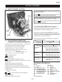
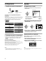
TRINITRON® COLOR MONITOR
9-978-884-01
Self Diagnosis
Supported model
HMD-A240
SERVICE MANUAL
HMD-A240
Trinitron
US/Canada Model
Chassis No: SCC-L38A-A
17VC CHASSIS
SPECIFICATIONS
Picture tube
0.24 mm aperture grill pitch (center)
17 inches measured diagonally
90-degree deflection
Video image area
(16.1" maximum viewing image)
Approx. 328 X 242 mm (w/h)
(13 x 95/8 inches)
Resolution
Horizontal: Max. 1280 dots
Vertical: Max. 1024 lines
Standard image area
Approx. 312 x 234 mm (w/h)
(123/8 x 91/4 inches)
Input signal
Video
Analog RGB (75 ohms typical)
0.7 Vp-p, ±5%, Positive
Sync
Separate HD/VD,
TTL Polarity Free
External Composite,
TTL Polarity Free
(2k ohms impedance)
Sync on Green
Power Consumption
100 W
Deflection frequency
Horizontal: 30 to 75 kHz
Vertical: 48 to 120 Hz
AC input voltage/current 100 to 120 V, 50/60 Hz, 1.7A
Dimensions
422 x 426 x 426 mm (w/h/d)
(161/2 x 165/8 x 165/8 inches)
Mass
Approx. 19 kg (41 lb 14 oz.)
Design and specifications are subject to change without notice.
TRINITRON® COLOR MONITOR
9-978-884-01
HMD-A240
TABLE OF CONTENTS
SECTION TITLE
PAGE
Power Management.................................................................................................................................. 4
Self Diagnosis Function ............................................................................................................................ 4
Timing SpeciÞcation.................................................................................................................................. 4
Warnings and Cautions............................................................................................................................. 5
Safety Check Out ..................................................................................................................................... 6
1. Disassembly
1-1. Cabinet Removal ............................................................................................................................... 7
1-2. Service Position................................................................................................................................. 7
1-3. A & D Board Removal........................................................................................................................ 8
1-4. Picture Tube Removal ....................................................................................................................... 9
Anode Cap Removal ......................................................................................................................... 9
2. Safety Related Adjustments
2-1. HV Regulator Check........................................................................................................................ 10
2-2. HV Protector Circuit Check.............................................................................................................. 10
2-3. Beam Protector Check (Software Logic) ......................................................................................... 10
2-4. B+ Voltage Check............................................................................................................................ 10
3. Adjustments
3-1. Landing Rough Adjustment ..............................................................................................................11
3-2. Landing Fine Adjustment ..................................................................................................................11
3-3. Convergence Rough Adjustment......................................................................................................11
3-4. Convergence and V. Key (H. TRP) Fine Adjustment ........................................................................11
3-5. Vertical and Horizontal Position and Size SpeciÞcation .................................................................. 12
3-6. Focus Adjustment ............................................................................................................................ 13
3-7. Digital Convergence Adjustment ..................................................................................................... 13
3-8. Convergence SpeciÞcation.............................................................................................................. 13
4. Diagrams
4-1. Circuit Boards Location ................................................................................................................... 14
4-2. Printed Wiring Board and Schematic Diagram Information ............................................................. 14
4-3. Block Diagram and Schematics
Block Diagrams ............................................................................................................................... 15
A Board - Schematic Diagram......................................................................................................... 17
D Board - Schematic Diagram ........................................................................................................ 19
H1 Board - Schematic Diagram ...................................................................................................... 23
J Board - Schematic Diagram ......................................................................................................... 24
4-4. Semiconductors............................................................................................................................... 25
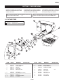
5. Exploded Views
5-1. Picture Tube .................................................................................................................................... 26
5-2. Chassis............................................................................................................................................ 27
5-2. Packing Materials ............................................................................................................................ 28
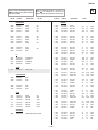
6. Electrical Parts List ....................................................................................................................................... 29
—3—
HMD-A240
POWER MANAGEMENT
The power saving mode complies with the VESA Display Power Management Signaling standard. Each state of power management shall be activated
by the host computer terminating the appropriate sync signals. Blanking the video must precede termination of the sync signals. The elapsed time
counter shall also be controlled by the host computer. Reactivation of the monitor shall be accomplished from the host computer by re-establishing the
normal sync signal.
Power consumption
mode
Screen
(video)
Horizontal
sync signal
Vertical
Power
sync signal consumption
Recovery time
Indicator
1
Normal operation
active
yes
yes
< 100 W
--
Green
2
Active-off (3rd mode)
blank
no*
no*
<3W
Approx. 10 sec.
Amber
3
Power-off
--
--
--
0 W (approx)
--
Off
* In this mode, the signal will appear in one of three ways: The Horizontal Sync Signal alone off, the Vertical Sync Signal
alone off, or both signals off.
SELF DIAGNOSIS FUNCTION
When a failure occurs, the STANDBY/TIMER lamp will ßash a set number of times to indicate the possible cause of the problem. If there is more than
one error, the lamp will identify the Þrst of the problem areas.
1
Status
Failure 1
2
3
Failure 2
Failure 3
4
Aging/Self Test
Area of Failure
HV or +B
H Stop, V Stop or S Correction FET Failure
ABL
LED Indication
Amber (0.5 second) / Off (0.5 second)
Amber (1.5 second) / Off (0.5 second)
Amber (0.5 second) / Off (1.5 second)
Amber (0.5 second) / Off (0.5 second)/
Green (0.5 second) / Off (0.5 second)
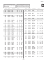
TIMING SPECIFICATION
PRIME
MODE
MODE
1
2
3
4
5
6
7
8
9
RESOLUTION 640 X 480 640 X 480 720 X 400 800 X 600 800 X 600 832 X 624 1024 X 768 1024 X 768 1280 X 1024
CLOCK
25.175
36
28.322
49.5
56.25
57.283
78.75
94.5
108
HORIZONTAL
H. FREQ
31.469
43.269
31.469
46.875
53.674
49.725
60.023
68.677
63.981
H. TOTAL
31.778
23.111
31.777
21.333
18.631
20.111
16.660
14.561
15.630
H. BLK
6.356
5.333
6.355
5.172
4.409
5.586
3.657
3.725
3.778
H. FP
0.636
1.556
0.636
0.323
0.569
0.559
0.203
0.508
0.444
H. SYNC
3.813
1.556
3.813
1.616
1.138
1.117
1.219
1.016
1.037
H. BP
1.907
2.222
1.907
3.232
2.702
3.910
2.235
2.201
2.296
H. ACTIV
25.422
17.778
25.422
16.162
14.222
14.524
13.003
10.836
11.852
VERTICAL
V. FREQ
59.940
85.008
70.087
75.000
85.061
74.550
75.029
84.997
60.020
V. TOTAL
16.683
11.764
14.268
13.333
11.756
13.414
13.328
11.765
16.661
V. BLK
1.430
0.670
1.557
0.533
0.578
0.865
0.533
0.582
0.656
V. FP
0.318
0.023
0.381
0.021
0.019
0.020
0.017
0.015
0.016
V. SYNC
0.064
0.069
0.064
0.064
0.056
0.060
0.050
0.044
0.047
V. BP
1.049
0.578
1.112
0.448
0.503
0.784
0.466
0.524
0.594
V. ACTIV
15.253
11.093
12.711
12.800
11.179
12.549
12.795
11.183
16.005
SYNC
INT (G)
NO
NO
NO
NO
NO
NO
NO
NO
NO
EXT (H/V) / POLARITY
YES
YES
YES
YES
YES
YES
YES
YES
YES
EXT (CS) / POLARITY
NO
NO
NO
NO
NO
NO
NO
NO
NO
SERRATION
NO
NO
NO
NO
NO
NO
NO
NO
NO
SYNC LEVEL
TTL
TTL
TTL
TTL
TTL
TTL
TTL
TTL
TTL
VIDEO
VIDEO LEVEL
0.7
0.7
0.7
0.7
0.7
0.7
0.7
0.7
0.7
SET UP
0
0
0
0
0
0
0
0
0
—4—
HMD-A240
WARNINGS AND CAUTIONS
CAUTION
Short circuit the anode of the picture tube and the anode cap to the metal chassis, CRT shield, or carbon painted on the CRT, after
removing the anode.
WARNING!!
An isolation transformer should be used during any service to avoid possible shock hazard, because of live chassis. The chassis of this
receiver is directly connected to the AC power line.
! SAFETY-RELATED COMPONENT WARNING!!
Components identiÞed by shading and ! mark on the schematic diagrams, exploded views, and in the parts list are critical for safe
operation. Replace these components with sony parts whose part numbers appear as shown in this manual or in supplements published
by sony. Circuit adjustments that are critical for safe operation are identiÞed in this manual. Follow these procedures whenever critical
components are replaced or improper operation is suspected.
ATTENTION!!
Apres avoir deconnecte le cap de l’anode, court-circuiter l’anode du tube cathodique et celui de l’anode du cap au chassis metallique de
l’appareil, ou la couche de carbone peinte sur le tube cathodique ou au blindage du tube cathodique.
AÞn d’eviter tout risque d’electrocution provenant d’un chássis sous tension, un transformateur d’isolement doit etre utilisé lors de tout
dépannage. Le chássis de ce récepteur est directement raccordé à l’alimentation du secteur.
! ATTENTION AUX COMPOSANTS RELATIFS A LA SECURITE!!
Les composants identiÞes par une trame et par une marque ! sur les schemas de principe, les vues explosees et les listes de pieces
sont d’une importance critique pour la securite du fonctionnement. Ne les remplacer que par des composants sony dont le numero
de piece est indique dans le present manuel ou dans des supplements publies par sony. Les reglages de circuit dont l’importance est
critique pour la securite du fonctionnement sont identiÞes dans le present manuel. Suivre ces procedures lors de chaque remplacement
de composants critiques, ou lorsqu’un mauvais fonctionnement suspecte.
—5—
HMD-A240
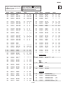
SAFETY CHECK-OUT
After correcting the original service problem, perform the following
safety checks before releasing the set to the customer:
1. Check the area of your repair for unsoldered or poorly soldered
connections. Check the entire board surface for solder splashes and
bridges.
2.
1.
A commercial leakage tester, such as the Simpson 229 or RCA
WT-540A. Follow the manufacturers’ instructions to use these
instructions.
2.
A battery-operated AC milliammeter. The Data Precision 245 digital
multimeter is suitable for this job.
3.
Measuring the voltage drop across a resistor by means of a VOM
or battery-operated AC voltmeter. The “limit” indication is 0.75
V, so analog meters must have an accurate low voltage scale.
The Simpson’s 250 and Sanwa SH-63TRD are examples of
passive VOMs that are suitable. Nearly all battery-operated digital
multimeters that have a 2 VAC range are suitable (see Figure A).
Check the interboard wiring to ensure that no wires are “pinched” or
touching high-wattage resistors.
3. Check that all control knobs, shields, covers, ground straps, and
mounting hardware have been replaced. Be absolutely certain that
you have replaced all the insulators.
4.
Look for unauthorized replacement parts, particularly transistors,
that were installed during a previous repair. Point them out to the
customer and recommend their replacement.
5.
Look for parts which, though functioning, show obvious signs of
deterioration. Point them out to the customer and recommend their
replacement.
6.
Check the line cords for cracks and abrasion. Recommend the
replacement of any such line cord to the customer.
7.
Check the B+ and HV to see if they are speciÞed values. Make sure
your instruments are accurate; be suspicious of your HV meter if
sets always have low HV.
8.
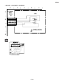
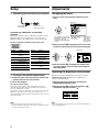
Leakage Test
The AC leakage from any exposed metal part to earth ground and from all
exposed metal parts to any exposed metal part having a return to chassis,
must not exceed 0.5 mA (500 microamperes). Leakage current can be
measured by any one of three methods.
Check the antenna terminals, metal trim, “metallized” knobs,
screws, and all other exposed metal parts for AC leakage. Check
leakage as described below.
How to Find a Good Earth Ground
A cold-water pipe is a guaranteed earth ground; the cover-plate retaining
screw on most AC outlet boxes is also at earth ground. If the retaining
screw is to be used as your earth ground, verify that it is at ground
by measuring the resistance between it and a cold-water pipe with an
ohmmeter. The reading should be zero ohms.
If a cold-water pipe is not accessible, connect a 60- to 100-watt troublelight (not a neon lamp) between the hot side of the receptacle and the
retaining screw. Try both slots, if necessary, to locate the hot side on the
line; the lamp should light at normal brilliance if the screw is at ground
potential (see Figure B).
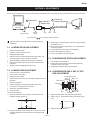
Parts on Set
0.15 µF
1.5 K Ω
AC
Voltmeter
(0.75 V)
Earth Ground
Figure A. Using an AC voltmeter to check AC leakage.
Figure B. Checking for earth ground.
—6—
HMD-A240
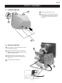
SECTION 1: DISASSEMBLY
1-1. CABINET REMOVAL
2
1 Remove (4) Screws (+BVTP 4 x 16)
2 Release top claws - Insert the tip of a ßathead
screwdriver approximately 0.25" to unlock the
claw. Gently lift up and then back to remove
the cabinet.
2
1
1-2. SERVICE POSITION
1 Gently wiggle the A board back and forth to unplug
it from the Neck Assembly.
1
2 Remove all necessary connections and rotate the
D Board and rest it on its side to expose the bottom.
Be sure to reconnect all wires.
3 Fabricate a temporary ground wire with a male
stakon connector on one end and an alligator clip
on the other.
4 Reconnect ground as shown below.
2
4
—7—
HMD-A240
1-3. A & D BOARD REMOVAL
3
5
1
2
1
Remove (1) screw (+BVTP 3 x 8) from the cable holder
at the rear of the chassis base to release the cable.
2
Remove (2) screws (+BVTP 3 x 8) from the rear of the D
Board and remove the rear of the chassis base.
3
Remove remaining (7) screws (+BVTP 3 x 8) from the D
Board. Lift the board up and out to remove.
4
Remove the shield cover from the A board.
5
Gently wiggle the A board back and forth, and pull it to
remove.
—8—
4
HMD-A240
1-4. PICTURE TUBE REMOVAL
1 Place the unit face down on a cushion to avoid
scratching.
2 Remove the anode cap.
3 Remove (4) screws (Screw (5) Tapping) from
the CRT.
Remove the A board.
4
5 Remove the neck assembly.
6 Remove the deßection yoke.
7 Remove (2) screws (BVTP 4 x 16) from the
base assembly and slide out to remove.
8 Remove the demagnetization coil.
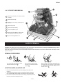
ANODE CAP REMOVAL
WARNING: High voltage remains in the CRT even after the power is disconnected. To avoid electric shock, discharge CRT before attempting to remove
the anode cap. Short between anode and coated earth ground strap of CRT.
NOTE: After removing the anode cap, short circuit the anode of the picture tube and the anode cap to either the metal chassis, CRT shield, or carbon
painted on the CRT.
REMOVAL PROCEDURES
c
b
a
Anode Button
Turn up one side of the rubber cap in the
direction indicated by arrow a .
Use your thumb to pull the rubber
cap Þrmly in the direction indicated
by arrow b .
HOW TO HANDLE AN ANODE CAP
1.
2.
3.
Do not use sharp objects which may cause damage to the surface of the
anode cap.
To avoid damaging the anode cap, do not squeeze the rubber covering too
hard. A material Þtting called a shatter-hook terminal is built into the rubber.
Do not force turn the foot of the rubber cover. This may cause the shatter-hook
terminal to protrude and damage the rubber.
—9—
When one side of the rubber cap separates from
the anode button, the anode cap can be removed
by turning the rubber cap and pulling it in the
direction of arrow c .
HMD-A240
SECTION 2: SAFETY RELATED ADJUSTMENTS
When replacing parts shown in the table below, the following
operational checks must be performed as a safety precaution
against X-ray emissions from the unit.
Part Replaced (
2-2. HV PROTECTOR CIRCUIT CHECK
1.
2.
)
RV501
HV ADJ
Part Replaced (
)
HV Regulator
Circuit
D Board T501, IC501, RV501, R540,
R541, R542, R544, R564, R567,
R568, C532, C534, C539, C553,
C554, C555, C556, C558, C561
HV HOLD
DOWN Circuit
D Board T501, R510, R543, R547, R549,
R552, R595, D515, D517, C540,
C542, C544, IC607, IC901, C951
Beam Current
Protector Circuit
D Board T501, R545, R546, R548, R550,
R596, R934, C535, C541, IC605,
IC607, IC901
Check Condition
• Input voltage: 120 ± 2 VAC
• Input signal:
(fH =69 kHz), White Cross Hatch
• Controls:
CONT (max) & BRT (center)
• B+ Voltage:
179 ± 3.0 VDC
2-3. BEAM PROTECTOR CHECK
(SOFTWARE LOGIC)
1.
Allow the unit to warm up for one minute prior to checking the
following conditions.
8.
2-4. B+ VOLTAGE CHECK
1.
2.
3.
4.
4
7.
Input white cross hatch signal (fH = 80 kHz).
CONT maximum and BRT center.
Cut off Screen VR (G2).
Input voltage: 120 ± 2 VAC.
ConÞrm that the voltage is within the voltage range shown below:
Standard voltage: 26.0 +0.3, -0.5 kV
When replacing components identiÞed by Y , make sure to recheck
the High Voltage.
Verify the High Voltage as shown above (26.0 +0.3, -0.5 kV) is
within speciÞcation. If not, set H. SIZE data at minimum (-127)
and then adjust RV501 on D Board (Adjustment target = 26.0 ±
0.2 kV).
After adjusting the High Voltage within speciÞcation, put the RV
cover on RV501 as shown below and apply sufÞcient amount of RTV
around RV501.
10
6.
Using an external current source, apply < 1.55mA between pin 11
of FBT (T501) and GND, and conÞrm that the raster fades out.
Check Condition
• Input voltage: 120 ± 2 VAC
• Input signal :
(fH = 69 kHz), White Cross Hatch
• Controls:
CONT (max) & BRT (center)
2-1. HV REGULATOR CHECK
1.
2.
3.
4.
5.
ConÞrm that the voltage between cathode of D517 and GND is
more than 27.0 VDC.
Using an external DC Power supply, apply the voltage shown below
between cathode of D517 on D Board and GND, and conÞrm that
the HV Hold-Down circuit works (Raster disappears). Apply DC
Voltage: Less than 35.9 VDC.
RV501
— 10 —
Input white cross hatch (fH = 69 kHz) signal.
CONT (max) & BRT (center).
Input voltage: 110 ± 10 VAC.
Note: Use NF power supply or make sure that distortion factor is
3% or less.
ConÞrm that the voltage is within the range shown below:
Standard voltage: 179 ± 3.0 VDC
HMD-A240
SECTION 3: ADJUSTMENTS
Connect the communication cable of the connector located on the D Board on the monitor. Run the service software and then follow the instructions.
1 1-690-391-21
2 A-150-919-A
Interface Unit
IBM at Computer
as a Jig
3 3-702-691-01
Connector Attachment
To BUS CONNECTOR
D-Sub
(9 Pin [female])
Mini Din
(8 Pin)
4 Pin
4 Pin
4 Pin
* The Parts above ( 1 - 3 ) are necessary for DAS Adjustment.
Allow a 30 minute warm-up period prior to making the following
adjustments.
13. Adjust V.Key (= H.Trapezoid) with H.TRP VR so that [a] is equal to
[b] (See Section 3-4.).
14. If the corner landing is out of speciÞcation, use a disk magnet for
the landing correction.
15. If disk magnets were used, perform an auto degauss.
16. Remove the wobbling coil and sensor.
17. Fix the purity magnet on DY with white paint.
3-1. LANDING ROUGH ADJUSTMENT
1.
2.
3.
4.
5.
6.
7.
Display the all white pattern.
Adjust the contrast to maximum value.
Display plain green pattern.
Slide the DY back and roughly adjust the plain green pattern with
the purity magnet so that it is centered on the screen.
Adjust HCENTER by HCENTER Volume (RV502 on D Board).
Moving the DY forward, adjust so that an entire screen becomes
pure green.
Adjust the DY tilt and lightly tighten the DY screw.
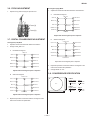
3-3. CONVERGENCE ROUGH ADJUSTMENT
1.
2.
3.
3-2. LANDING FINE ADJUSTMENT
1.
2.
3.
4.
Place the monitor in the Helmholtz coil.
Set TLH plate to zero position.
Display plain green pattern.
Degauss CRT face and iron parts with degauss equipment or handdegausser.
5. Perform auto degauss.
6. Attach a wobbling coil to the speciÞed position of CRT neck.
7. Put the sensor of landing checker to CRT face.
8. Adjust purity, DY position and DY tilt.
9. Tighten DY screw.
10. Perform auto degauss.
11. Adjust top and bottom pin by pitching DY up and down with two
wedges so that [a] is equal to [b].
Enter the white crosshatch signal.
Roughly adjust the horizontal (H.STAT) and vertical (V.STAT)
convergence at four-pole magnet.
Roughly adjust HMC and VMC at six-pole magnet.
3-4. CONVERGENCE AND V. KEY (H. TRP)
FINE ADJUSTMENT
Neck Ass'y
H-TRP VR TLV VR
Purity
XCV VR
Magnet
A Board
DY
6-pole 4-pole
YCV VR
Mg
Mg
TB Pin VR
TLH Plate
1.
2.
[a]
Display crosshatch pattern with green lines and black Þeld.
Adjust V. Key (=H. Trapezoid) with H.TRP VR so that [a] is equal
to [b].
[a]
3.
[b]
CRT
12. Adjust top and bottom pins to zero with TB. H.PIN VR. Also, V.SIZE
should be adjusted at the same time becasue it is changed by TB.
H.PIN VR.
— 11 —
Adjust the TB Pin with TB Pin VR.
[b]
HMD-A240
TB Pin Movement
14. Adjust XCV with XCV VR.
XCV Movement
B
R
4.
5.
6.
7.
Adjust V.SIZE with "VSIZE".
Change "CONV_SW" to "0" and "MCR2" to "153".
Display crosshatch pattern with red and blue lines and black Þeld.
Adjust H.STAT and V.STAT with 4 pole magnet. Use 4 pole magnet,
not "HSTAT" and "VSTAT".
15. Adjust YCH with YCH VR.
YCH Movement
4 Pole Magnet
1
R
1
1
B
2
2
16. Adjust V.TILT with TLV VR.
TLV Movement
B
R
B
1
1
1
B
R
R
B
R
2
R
B
2
R
B
2
8.
9.
2
RB
B
R
Display crosshatch pattern with white lines and black Þeld.
Adjust HMC and VMC with 6 pole magnet.
6 Pole Magnet
17. If necessary, repeat steps 3-14 to make the optimum condition for
the entire screen.
18. Fix 4-pole magnet, 6-pole magnet, TLH plate and XCV VR with
white paint.
Zero Position Neck Ass'y
2
4-Pole Mg
Purity
1
6-Pole Mg
G
2
G
1
3-5. VERTICAL AND HORIZONTAL POSITION
AND SIZE SPECIFICATION
a
10.
11.
12.
13.
Display crosshatch pattern with red and blue lines and black Þeld.
If necessary, repeat steps 5-8.
Change "CONV_SW" to "6".
Adjust H.TILT with TLH plate.
TLH Movement
R B
A
B R
fH 0kHz
2.0 mm
2.0 mm
fH 60kHz
2.4 mm
2.4 mm
A
B
234 312
B
b
— 12 —
a
b
HMD-A240
3-6. FOCUS ADJUSTMENT
1.
Convergence (High) Mode
1. Adjust the H.STAT and V.STAT with "HSTAT-HI" and "VSTAT-HI".
Adjust Focus (V) and Focus (H) for optimum focus.
A.
Horizontal Convergence
YBH-T-HI
CBH-T-HI
9
10 CBH-T-R-HI
5
18 MBH-T-R-HI
MBH-T-L-HI 17
2 APH-R-HI
APH-L-HI 1
Focus (V)
HSTAT-HI
20 MBH-B-R-HI
MBH-B-L-HI 19
CBH-B-L-HI 11
Focus (H)
6
12 CBH-B-R-HI
YBH-B-HI
Adjust each misconvergence point in sequence.
3-7. DIGITAL CONVERGENCE ADJUSTMENT
B.
Convergence (Low) Mode
1. Adjust the H.STAT and V.STAT with "HSTAT" and "VSTAT".
2. Change "CONV_SW" to "7".
A.
CCV-T-L-HI 13
XBV-L-HI
8
16 CCV-B-R-HI
V STAT-B-HI
2 APH-R-LO
Adjust each misconvergence point in sequence.
HSTAT
20 MBH-B-R-LO
MBH-B-L-LO 19
CBH-B-L-LO 11
6
12 CBH-B-R-LO
2.
YBH-B-LO
Adjust each misconvergence point in sequence.
3.
Repeat the procedure of A and B so that the convergence of the
entire screen is within the speciÞcation.
Change "MCR2" to "170".
3-8. CONVERGENCE SPECIFICATION
Vertical Convergence
V STAT-T-LO
7
14 CCV-T-R-LO
B
A
XBV-L-LO 3
4 XBV-R-LO
V STAT
24 MCV-B-R-LO
MCV-B-L-LO 23
8
16 CCV-B-R-LO
V STAT-B-LO
312 mm
Adjust each misconvergence point in sequence.
Repeat the procedure of A and B so that the convergence of the
entire screen is within the speciÞcation.
— 13 —
234 mm
22 MCV-T-R-LO
MCV-T-L-LO 21
3.
XBV-R-HI
24 MCV-B-R-HI
MCV-B-L-HI 23
18 MBH-T-R-LO
APH-L-LO 1
CCV-B-L-LO 15
4
10 CBH-T-R-LO
5
MBH-T-L-LO 17
CCV-T-L-LO 13
22 MCV-T-R-HI
3
CCV-B-L-HI 15
B.
14 CCV-T-R-HI
V STAT-HI
YBH-T-LO
9
V STAT-T-HI
7
MCV-T-L-HI 21
Horizontal Convergence
CBH-T-LO
Vertical Convergence
A Zone:
Primary Mode
H: < 0.25 mm
V: < 0.25 mm
Others
H: < 0.3 mm
V: < 0.3 mm
B Zone:
Primary Mode
H: < 0.3 mm
V: < 0.3 mm
Others
H: < 0.4 mm
V: < 0.4 mm
HMD-A240
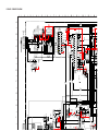
SECTION 4: DIAGRAMS
4-1. CIRCUIT BOARDS LOCATION
The components identiÞed by shading and ! symbol are critical for safety. Replace
only with part number speciÞed.
A Board
indicates a fast operating fuse and is displayed on the component
The symbol
side of the board. Replace only with fuse of the same rating as marked.
Les composants identiÞes per un trame et une marque ! sont critiques pour la
securite. Ne les remplacer que par une piece portant le numero speciÞe.
Le symbole
indique une fusible a action rapide. Doit etre remplace par une
fusible de meme yaleur, comme maque.
The components identiÞed by X in this basic schematic diagram
have been carefully factory-selected for each set in order to
satisfy regulations regarding X-ray radiation. Should replacement be
necessary, replace only with the value originally used.
J Board
When replacing components identiÞed by Y, make the necessary
adjustments as indicated. If the results do not meet the speciÞed value,
change the component identiÞed by X and repeat the adjustment until
the speciÞed value is achieved. (See page 10)
H Board
D Board
When replacing the parts listed in the table below, it is important to
perform the related adjustments.
Part Replaced ( )
4-2. PRINTED WIRING BOARD AND
SCHEMATIC DIAGRAM INFORMATION
RV501
HV ADJ
All capacitors are in µF unless otherwise noted. pF : µµF 50WV or less
are not indicated except for electrolytics and tantalums.
All electrolytics are in 50V unless otherwise speciÞed.
All resistors are in ohms. kΩ=1000Ω, MΩ=1000kΩ
Part Replaced (
HV Regulator
Circuit
D Board T501, IC501, RV501, R540,
R541, R542, R544, R564, R567,
R568, C532, C534, C539, C553,
C554, C555, C556, C558, C561
HV HOLD
DOWN Circuit
D Board T501, R510, R543, R547, R549,
R552, R595, D515, D517, C540,
C542, C544, IC607, IC901, C951
Beam Current
Protector Circuit
D Board T501, R545, R546, R548, R550,
R596, R934, C535, C541, IC605,
IC607, IC901
Indication of resistance, which does not have one for rating
electrical power, is as follows: Pitch : 5mm
Rating electrical power : 1/ 4 W
1
/ 4 W in resistance, 1/10 W and 1/ 8 W in chip resistance.
: nonßammable resistor.
: fusible resistor.
: internal component.
: panel designation and adjustment for repair.
All variable and adjustable resistors have characteristic curve B, unless
otherwise noted.
Readings are taken with a color-bar signal input.
Readings are taken with a 10MΩ digital multimeter.
Voltages are DC with respect to ground unless otherwise noted.
Voltage variations may be noted due to normal production tolerances.
All voltages are in V.
S : Measurement impossibillity.
: B+line.
: B-line (Actual measured value may be different).
: signal path (RF).
Circled numbers are waveform references.
)
REFERENCE INFORMATION
RESISTOR
: RN
METAL FILM
: RC
SOLID
: FPRD NONFLAMMABLE CARBON
: FUSE NONFLAMMABLE FUSIBLE
: RW
NONFLAMMABLE WIREWOUND
: RS
NONFLAMMABLE METAL OXIDE
: RB
NONFLAMMABLE CEMENT
:
ADJUSTMENT RESISTOR
COIL
: LF-8L MICRO INDUCTOR
— 14 —
CAPACITOR
: TA
TANTALUM
: PS
STYROL
: PP
POLYPROPYLENE
: PT
MYLAR
: MPS METALIZED POLYESTER
: MPP METALIZED POLYPROPYLENE
: ALB BIPOLAR
: ALT HIGH TEMPERATURE
: ALR HIGH RIPPLE
HMD-A240
4-3 BLOCK DIAGRAMS AND SCHEMATICS
BLOCK DIAGRAM (1/2)
TO D BOARD
CN606
CN304
STBY +5V
+5V
10
CN302
5
15
4
14
8
3
BGND
1
BLUE
2
GGND
7
20
9
12
6
G-OUT
GREEN
4
RGND
5
G-IN
B-OUT
RED
6
R-OUT
CRT DRIVE
9
G-IN
27
IC002
+12V
+5V
7
GND
6
+12V
5
H1
4
GND
3
G-OUT
J001
+80V
+80V
3
2
NC
+180V
1
+180V
1
11
B-IN
4
B-OUT
H
11
8
STBY +5V
5
8
R-IN
24
B-IN
3
13
2
R-OUT
C SYNC
SIGNAL IN
7
1
30
9
7
R-IN
KR
8
11
12
CONNECTOR
PRE-AMP
CLAMP
KG
9
IC001
KB
TO JOO1
G2
BLK
15PIN D-SUB
R-OSD
IICSDA
GND
TO D BOARD
CN902
IC003
7
5
4
HRTRC
15
CN306
R-OSD
5
G-OSD
14
14
4
13
13
12
17
G-IN
3
10
2
5
SW
VFLB
IC004
CN301
9
B-OUT
TO D BOARD
1
SDA
2
1
1.2KV
HFLB
Q006
SDA
SCL
7
CN307
8
1
(VIDEO)
9-978-884-01<17VC>BLK 1OF2
— 15 —
HV
(TO FBT)
OSD-BLK
SCL
TO D BOARD
CN510
5
B-IN
-33V
8
G-OUT
B-OSD
B-BKG
OSD-BLK
1
R-OUT
CUTOFF AMP
G-OSD
4
B-OSD
7
R-IN
G-BKG
3
1
3
R-BKG
6
BPCLP
VRTRC
15
OSD
8
IICSCL
CBLK
3
10
CN309
C SYNC
PICTURE TUBE
A BOARD
G1
18
GND
FBT
HMD-A240
BLOCK DIAGRAM (2/2)
CONV-CONTROL
CN701
8P
CY4CY4+
4
IC701
6
10
9
9
CY3-
8
CY3+
7
SCONV OUT
IC703
7
9 V-STATICOUT
3
CY2-
6
CY2+
5
CY1CY1+
6 V-CONVOUT
7 H-CONVOUT
1
3
2
ROTATION+
1
3
DCONV OUT
IC702
3
13
2
V-SIN
2
6
4
ROTATION-
V.REF
IN
8 H-STATICOUT
1
CN510
VPOSIN
16
5
SDA
17
HD.IN
SCL
14
1
HST
T505
V.REF OUT
4
-33V
TO A BOARD
CN306
5
BUFFER
4
Q521
ROTATION
3
4
CN902
FROM
H RTRC
CONNECTOR
V RTRC
2
CBLK
3
BPCLP
4
IIC SCL
5
GND
TO A BOARD
15PIN D-SUB
CN309
1
V.DIV
SDA
7
CSYNC
8
V.SIN
7
SCL
46
22
36
ROTATION
23
EPROM
CBLANK
37
28
IC401
OUT
5
-IN
V.SAW
3
V-OUT
+IN
1
8
Q525
V-REF
IC905
FBT
BPCLAMP
12
3
DEF. CONTROL
CLK
B4+
IC902
6
IIC SDA
10
27
2
IC502
OP2+
T501
B3O
HV
HV-REG
18
TO CRT
Q503
DATA
H-REG
20
C-SYNC
PWM-CONT
B1O
Q520
RV501
IC501
10
5
15
4
14
SIGNAL IN
DDC SDA1
13
DDC SCL1
7
2
12
GND
6
1
/STBY 5V
HOST 5V
11
RESET
B2O
34
2
35
3
4
STBY +5V
HSYNC
6
7
DDCSCL
LOCK
IC901
23
2
28
27
26
H-OUT
EPROM
H-SYNC
STBY +5V
5
STBY 5V
5
GND
4
KEY
3
2
LED RED
2
1
LED GRN
3
S1003
4
13
HDT
T504
17
H.DRIVE
H.DRIVE OUT
H.OUT
Q903,Q501,Q502
Q511
Q507
12
V. DEF
14
CN501
6
5
SYNC LOCK
4
3
STBY +5V
PB1
15
48
PB4
DA3
18
4
PA5
47
1
MENU
RXD
3
TXD
4
PB3
38
REMOTE ON/OFF
RXD
DEGAUSS
TXD
Q525
PIN 1
5
6
180V
DFT
SRT
49-53
7
SWITCH
15V
CHANGE
LCT
T506
T503
80V
T601
TO S-CAP
DEGAUSS
Q519
BUFF
V DF-AMP
Q505
Q504
TO A BOARD
CN304
1
+12V
Q601
HEATER
SW
SW-REG CONT
1
DRIVE
IC601
NC
2
NC
3
VIN
DGC1
4
1
DGC
H OUT
16
S0-S4
STBY +5V
DGC2
4
SW-REG
5
Q602
Q603
REG
IC602
VCNTRL
+180V
4
OUT
ISENSE
CN606
HEATER
+80V
OOB
14
9
LFT
STBY CNTRL
LF602
Q605
+12V
S-CAP CHANGE
Q512,Q513,Q514
+5V
STBY +5V
5V,12V REG
+15V
IC605,608
12V
AC-RECT
5V REG
5V
OUT
+12V
OUT
+5V
IN1,2
DISABLE
IC607
CN1001
5P
S1001
D601
1
3
ERROR AMP
1
IC604
PHOTOCOUPLER
RCC CONTROL
PROTECT
IC603
Q604
12V
STBY
ON
1
STBY
CNT
2
STBY
OFF
3
MAIN
ON
4
MAIN
CNT
5
2
4
6
1
3
5
(
POWER
CONVERGENCE
)
3
1
9-978-884-01<17VC>BLK 2OF2
STBY ON
MAIN ON
STBY CNT
STBY OFF
MAIN CNT
CN607
5P
2
5
(POWER SWITCH)
4
THP600A
2
— 16 —
+180V
NC
3
+80V
GND
5
H1
6
+12V
7
CN600
AC IN
CN602
1
2
4
-15V
12V
THP600
V DYV DY+
STBY +5V
39
DOWN
NC
2
1
Q508
DA4
2
NC
H DY-
H OUT
PA6
1
DGND
STBY +5V
H DY+
L503
Q522,Q524
CN901
S1007
CN301
32
V-SYNC
TO CN901
RIGHT
TO A BOARD
HFB
20
UP
LEFT
SV
H.FLY
H-IN
CN904
4
H.OUT
V-IN
REF
PH2
8
25
26
V-OUT
30
LOCK
V RTRC
DDCSDA
IC906
SYNC INV.
5
H-DRIVE
CPU
PCI
IC908
FRONT PANEL
HV-OUT
Q510
33
1
VSYNC
CN801
19
IC904
CN903
HOST GND1
8
3
54
RESET
GND
8
+5V
9
STBY +5V
HMD-A240
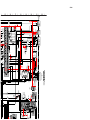
A BOARD - SCHEMATIC DIAGRAM
1
|
2
|
3
|
4
|
5
|
6
|
7
|
8
|
9
|
10
|
11
|
12
|
13
|
14
|
D311
1PS226-115
PROT.
G2
R317
56
25
23
2
4
21
R OUT
R009
10k
:CHIP
R_OSD
GND1
B_OUT
C206
0.1
250V
:MPS
8.2
R
R206
B_OUT
+B
5
R_OUT
4
7
8
9
11
C018
2.2
250V
C102
0.1
250V
:MPS
C054
0.1
250V
:MPS
R351
47
1/2W
:SURGE
C306
0.1
250V
:MPS
D306
HSS82
:CLAMP
FB301
D206
HSS82
:CLAMP
R251
47
1/2W
:SURGE
D106
HSS82
:CLAMP
R151
47
1/2W
:SURGE
R109
470k
:CHIP
R209
470k
:CHIP
R309
470k
:CHIP
R102
470k
:CHIP
R202
470k
:CHIP
R302
470k
:CHIP
+180V
R032
100k
:CHIP
C302
0.1
250V
:MPS
C202
0.1
250V
:MPS
R307
1k
:RN-CP
R208
9.1k
:RN-CP
R308
9.1k
:RN-CP
R033
330k
FB008
JW(5)
STBY 5V
C022
47
25V
FB010
6
IICSCL
5
BPCLP
4
R021
FB009
FB016
5.0 MM
47
R020
47
R018
100
R017
100
R006
100
R024
2.2k
:CHIP
:CHIP
STBY+5V
L001
JW(5)
C092
0.01
B:CHIP
FB006
+12V
R028
2.2k
:CHIP
:CHIP
12V
C001
1000p
500V
B
FB005
C002
1000p
500V
FB017
4.2
5.0 MM
:CHIP
1
0.2
R052
10k
:CHIP
—
C013
1000p
500V
:B
Q006
2SC2412K
:BUFFER
(VIDEO)
H
9-978-884-01<17VC>A BOARD
A—
BOARD IC VOLTAGE LIST
pin
1
2
3
4
5
I
IC001
volt
4.7
4.5
2.5
2.3
2.8
6
7
8
9
10
11
12
NC
2.1
4.7
2.1
3
2
0.07
13
14
15
16
17
18
19
0
0
0
11.9
0
0.8
GND
20
21
22
23
24
25
26
2.1
3.3
11.9
GND
2
3.3
GND
27
28
29
30
1.9
3.3
11.9
0.06
pin
1
2
3
4
5
IC002
volt
56.6
GND
56.3
GND
54.4
6
7
8
9
10
11
79.4
GND
2.1
2.0
11.9
2
pin
1
2
3
4
5
IC003
volt
0.5
1.0
1.0
5.0
4.2
6
7
8
9
10
11
12
5.0
4.7
4.5
5.0
0
NC
0
13
14
15
16
0
0
0
GND
pin
1
2
3
4
5
IC004
volt
GND
11.9
4.8
4.8
4.8
6
7
8
9
10
11
—
J
STBY 5V
8
+5V
GND
5
4
NC
67.3
61.0
62.4
NC
178.8
All voltages are in V
— 17 —
+12V
H1
GND
3
+80V
2
NC
1
3
2
9
7
6
C016
47
25V
:CHIP
:CHIP
CN304
9P
WHT
(L TYPE)
D001
1SR139
9
8
7
CN307
1P
R108
9.1k
:RN-CP
R207
1k
:RN-CP
G2
KR
KG
G1
G4
GM
HV
TO
A BOARD
SG002
SG201
L005
FB201
G_OUT
R_IN
G_IN
VCC
3
KB
TO D BOARD
FBT
SG101
VDD
8
R048
2.2M
1W
1.2KV
CN307
D205
HSS82
:PROTECTION
R014
100
:CHIP
10
7
VFLB
IICSDA
1
FB001
12
11
6
INT
SCL
C SYNC
CBLK
C305
0.1
25V
B:CHIP
SDA
CN309
8P
HRTRC
13
4
5
OSD_BLK
CN301
NEW
12
SS
R001
0
:CHIP
TO D BOARD
CN902
VRTRC
C205
0.1
25V
B:CHIP
HFLB
R051
1k
:CHIP
GND
14
3
G_OSD
VDDA
2
R107
1k
:RN-CP
RP
R005
330k
:CHIP
1
C053
0.1
25V
B:CHIP
C105
0.1
25V
B:CHIP
15
R003
8.2k
:CHIP
L002
0
F
G
16
1
2
VCO
B_OSD
—
R306
8.2k
:RN-CP
VSSA
VSS
6
7
11
R064
JW(15)
V901
PICTURE
TUBE
H
5
KR
KR
8
SG301
IC004
H8D2957
:CUT-OFF AMP
IC003
CXD9620P
:OSD
R002
C042
560
1000p
:CHIP B:CHIP
KG
H
6
7
TO D BOARD
CN510
D105
HSS82
:PROTECTION
C050
0.1
25V
B:CHIP
—
C044
100p
B:CHIP
GND2
VCC
R_OUT
D204
HSS82
:PROTECTION
B_IN
VCC R
9
8
D305
HSS82
:PROTECTION
16
15
R OSD
9
RCV
G1
FB101
17
14
G OSD
5
10
+80V
D304
HSS82
:PROTECTION
C106
0.1
250V
:MPS
IC001
CXA2067AS
:PRE-AMP
—
C035
0.0047
2kV
:B
18
13
B OSD
C046
0.01
B:CHIP
G_OUT
R_IN
D104
HSS82
:PROTECTION
10
SG001
H 4
4
11
KB
L305
L205
R117
56
OSD BLK
C047
47
25V
G2
10
R311
100
:FPRD
C036
1000p
500V
BLK
E
R211
100
:FPRD
C011
0.1
100V
12V
C007
470
16V
CLAMP
L007
R004
1.8k
:CHIP
1
L105
R GND
D
2
3
11G2
CN306
1
G1
+180V
12
R104
22
:CHIP
19
11
R IN
3
FB003
C304
0.1
25V
B:CHIP
S/H R
20
1
C112
15pF
—
VCC G
SYNC IN
C004
0.01 B:CHIP
4
R111
100
:FPRD
22
G IN
10
R119
1M
:CHIP
5
C014
47
100V
C012
0.1
25V
B:CHIP
G GND
C212
15pF
C
6
R217
56
G OUT
C010
0.1
25V
B:CHIP
7
24
7
C009
1000
10V
8
C204
0.1
25V
B:CHIP
S/H G
5
9
R219
1M
:CHIP
+5V
C312
12pF
R319
1M
:CHIP
R218
75
:CHIP
B IN
8
STBY 5V
—
C015
0.1
25V
B:CHIP
B GND
SIGNAL IN
3
9
3
FB004
R BKG
10
13
C003
1000p
500V
SG003
1
+80V
15PIN D-SUB
G BKG
B OUT
R130
75
:CHIP
11
R304
22
:CHIP
RCV
IC002
LM2415T
:VIDEO OUTPUT
30
6
FB102
0
:CHIP
R161
75
CONNECTOR
C104
0.1
25V
B:CHIP
S/H B
C151
0.1
25V
B:CHIP
11
VCC B
B BKG
GND3
R230
10
:CHIP
VBIAS
D111
1PS226-115
PROT.
FB202
0
:CHIP
G_IN
R261
75
R204
:CHIP
5
6
C049
0.1
25V
B:CHIP
22
RED
SCL
GND
B
4
R.GND
6
1
3
GREEN
B_IN
12
2
G.GND
29
7
C. SYNC
28
13
3
C251
0.1
25V
B:CHIP
SDA
27
—
2
9
J001
G3
12
8
7
26
BLUE
8
2
1
R330
75
:CHIP
2
14
4
D211
1PS226-115
PROT.
R361
75
1
3
B.GND
1
CN302
6P
15
4
10
5
FROM FBT
R030
1k
5
FB302
0
:CHIP
|
FROM FBT
C351
0.1
25V
B:CHIP
6
A
15
+180V
TO D BOARD
CN606
TO
D BOARD
CN302
B .G ND
G .G ND
B LU E
G RE EN
R .G ND
R ED
C046
R361
IC003
L002
R006
FB006
16
CN310
FB202
C251
FB302 C351
D111
15
C050
R009
FB010
FB017
R019
C151
R130
R018
R119
16
1
FB008
R002
R161
L007
FB016
C S YNC
I IC SDA
GND
I IC SCL
C BL K
BP CL P
V RTR C
H RTR C
R004
R005
S TBY 5V
+5 V
GN D
+ 12V
CN303
9
8
C012
R230
R047
R046
C023
1
30
JR8
C003
C028
R050
L105
B
C030
R048
CN301
1. 2K V
R053
G1
1
E
1
R208
FB002
R108
Q001
C035
R206
R064
SG001
R308
C305
C202
SG301
C205
R351
R251
FB101
R151
R202
SG201
L205
CN307
R305 L305
D204
C006
D304
C036
SG002
D104
R105
R211
R311
C037
R306
2
CN308
FB003
C039
D105
C055
C051
SG003
C011
CN306
C307
C015
R032
IC005
C029
R040
R317
C027
C049
C104
11
10
C107
R304
R217
IC002
C207
R104
IC001
R319
R049
C204
C010
JR2
JR7
R030
R024
D311
C212
C004
R219
C304
R021
R017
R020
C092
R001
R051
C016
FB001
C302
C054
R302
D206
D106
C306
R309
11
C106
R109
R102
C206
JW15
CN304
H1
JW17
1
CONDUCTOR SIDE
4
1-680-912-21
+1 80 V
GND
C002
FB005
+ 80 V
4
(1-719-642-21)
NC
1-680-912-21
C014
C013
+ 80V
— 18 —
G ND
H1
+ 12V
FB008
1
(1-719-642-21)
C011
FB001
FB004
514-A
CN308
JW20
GND
+ 5V
STB Y 5 V
9
CN303
FB006
C047
L002
IC003
3
C016
JW24
8
16
C014
R033
A-1299-
D205
C036
C022
C BLK
HRT RC
VRT RC
8
CN305
JW22
R111
JW21
L005
FB003
R311
10
11
JW18
JW14
FB005
3
D304
2
IC002
JW19
9
1
1
CN306
L001
FB017
BPC LP
I ICS CL
7
L105
D105
C007
FB009
L305
D104
R211
SG003
C206
SG002
SG001
L205
C006
JW11
JW13
2
CN307
D204
G1
C003
J001
G ND
I IC SDA
C013
2
JW23
C106
D106
SG101
D014
R151
R117
FB101
FB010
FB016
D
R217
JW9
6
NC
A
JW7
L007
1
R317
JW8
R161
E
SG201
D
D206
D306
R251
JW10
1
16
15
RED
R. GN D
R261
30
JW6
JW1
1
IC001
JW4
B LUE
GR EEN
G. GND
CN302
NC
1
C018
C306
1. 2K V
JW5
SG301
CN301
C009
B. GND
CN310
CN304
1
FB201
R064
R053
JW3
JW2
C
R351
C102
FB002
R048
B
R361
C035
E
Q001
B
FB301
1
B
C202
C302
C028
E
11
A
C054
IC004
C
+ 18 0V
A
[Video]
HMD-A240
COMPONENT SIDE
5
D001
1
2
D305
.725 Vp-p (H)
7
9
5
Q006
.705 Vp-p (H)
3
4
.701 Vp-p (H)
3.188 Vp-p (H)
5
6
2.938 Vp-p (H)
2.769 Vp-p (H)
12
8
40.94 Vp-p (H)
11
JW16
38.75 Vp-p (H)
10
C001
35.94 Vp-p (H)
CN309
A BOARD LOCATOR LIST
DIODE
D001
D104
D105
D106
D111
D204
D205
D206
D211
D304
D305
D306
D311
COMP COND
A-4
-B-3
-B-3
-A-3
--D-4
B-3
-A-4
-A-3
--D-4
B-4
-A-4
-A-2
--D-5
IC001
IC002
IC003
IC004
COMP COND
D-2
-C-4
-D-3
-B-1
--
IC
TRANSISTOR
COMP COND
-D-2
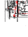
D BOARD - SCHEMATIC DIAGRAM
1
HMD-A240
|
2
|
3
|
4
|
5
|
6
|
7
|
8
|
9
|
10
|
11
|
12
|
13
|
14
|
15
|
16
|
17
|
18
|
19
|
20
|
21
|
22
|
TO H1 BOARD
CN801
CN904
5P
IIC SCL
IIC SDA
5
4
1
2
56
3
55
54
1
2
3
GND
1k
LOCK
C939
100p
CH:CHIP
41
VSI2
SCL
TXD
RXD
IIC SDA
IIC SCL
DDC SDA
DDC SCL
PD4
PC1
HOST GND1
PD3
HFB
H FLY
VSO
VDD
HSO
CSI
HSI1
VSS
H-SYNC
C909
100
16V
V.DF
H FLY
E/W
8
R969
100
9
IC908
TC74HCT04AF
SYNC INVERTER
L902
10
11
12
13
R940
47k
:CHIP
HD
6
5
4
3
R906
10k
14
2
100
ABL
R938
CSYNC
100
100
:CHIP
D901
UDZS-TE17-5.6B
HD
REMOTE SW
LOCK
C546
220p
CH:CHIP
C618
0.1
:PT
O
R600
1
10W
CN602
2P
IC604
AS431LAN
ERROR AMP
C643
4700p
250V
C605
0.22
250V
2
2
3
1
4
STBY 5V
R609
3.9k
:RN-CP
5V-2
STBY
5V
12V
R628
9.1k
:RN-CP
R649
2.2k
:RN-CP
3
2
1
C630
1.0
10V
C601
47
10V
R697
1.2
1W
:RS
D603
1SS119-25TD
R607
22k
:CHIP
R502
200k
:RN-CP
C682
0.47
25V
F:CHIP
R501
100
C501
10
13
0.63
0
R503
10k
:RN-CP
CLP005
C653
1000p
B:CHIP
R571
6.8k
:CHIP
H FLY
5
6
C504
330p
500V
B
C571
22p
2kV
0.69
C503
0.01
B:CHIP
Q505
2SA1037
BUFFER
PWR CONT
IC501
R
R
R
REF
R534
:FPRD
R552
56k
:RN
H RTRC
C544
0.01
:PT
R599
1k
:CHIP
D517
HZT33-02TE
L510
HCC
0
Q521
2SA1037AK
SW
3
6
4
5
R595
220k
:RN
C542
10
50V
4
5
C564
0.47
B:CHIP
R529
82
2W
R526
82
2W
8
9
10
C554
0.1
25V
B:CHIP
11
12
C561
0.001
B:CHIP
C576
47p
CH:CHIP
R583
10k
R541
1k
:RN
53.2
13
178.1
R574
2.2k
R543
4.7
:FPRD
L507
JW(5)
HV
Q510
STP4NB80FP
HV OUT
12
270V-2
C550
470
16V
C534
0.033
100V
T501
S
C519
1200p
2kV
:PP
NEW
:FBT
1
FV1
D504
NNCD12A-T1
R597
2.2M
R568
47k
R540
200k
:RN
C539
0.01
100V
16
C532
0.22
100V
R542
1k
:RN
RV501
100k
C556
220p
CH:CHIP
R544
270k
7
D515
ERA34-10TP1
15
6
SG501
D510
D1NL40-TA
SV
4
C533
1.0
50V
R539
10k
:RN
D503
HZT33-02TE
C537
100p
500V
R532
2.2
:FPRD
C528
0.01
200V
:PT
14
FV2
3
5
R570
10k
1/2W
:SURGE
12V
R548
1.2k
:RN
8
11
D531
D1NL20U
7
C548
0.001
:PT
C563
470p
B:CHIP
C535
0.1
:PT
9
PS501
500MA
IC LINK
6
R557
18k
:CHIP
C552
0.01
B:CHIP
R584
4.7k
:CHIP
R520
100
:FPRD
R547
220k
:RN
C540
0.01
630V
R549
62k
:RN
3
R553
91k
:RN-CP
2
L502
FB502
0UH
11
4.91
CLP003
100
R531
3W :RS
C526
2200p
500V
L501
D513
D1NL40
H FLY
2
D530
D1NL20U
10
12
D514
HSS82
R546
33k
:RN
R550
1.2k
:RN
R596
1.2k
:RN
R545
47k
:RN-CP
C541
4.7
RV502
100
L505
4.7mH
C514
1
250V
:PP
5
7
8
3
R512
4.7
0.12
C507
0.3
400V
C511
250V
C516
0.24
250V
:PP
C572
4.7
250V
0.068
0
C512
0.01
B:CHIP
C523
0.082
250V
:PP
C531
0.047
250V
:PP
C530
250V
L506
3.9mH
STBY
5V
:PP
:PP
5.01
R515
1k
:FPRD
C505
JW(7.5)
1
R575
100
1/2W
:FPRD
D511
D1NL40-TA
4
2
R507
2.7k
:RN
CP3
R
12V
53.2
R527
10k 178.1
C527
0.01
250V
8
C506
0.01
B:CHIP
145.2
1.23
CP2
R
R
C582
0.022
B:CHIP
C543
100p
CH:CHIP
R530
82
3W
:RS
82
12V
1
R561
82
3W
:RS
S
R572
0.47
1/2W
:FPRD
C524
33
200V
Q525
2SC2412K
H.OUT
R590
22k
:RN-CP
Q503
2SJ449
HV REG
D509
NNCD12A-T1
C575
33
200V
H RTRC
4
3
1
8
R581
10k
R582
33
:FPRD
R587
1k
:CHIP
0.5
S
4
V SAW
FB504
0UH
0.9
0.9
C517
0.01
:PT
R591
150
1/4W
:RN
D519
MTZJ-T-77-5.6B
R506
330k
:RN
R505
10k
R516
150
1/4W
:RN
R528
2.2k
:CHIP
13
C515
0.01
B:CHIP
S
Q514
2SK2098
S CAP CHANGE
19.9
R521
1k
0.4
:FPRD
R519
1M
R525
1k
:FPRD
S
Q513
2SK2098
S CAP CHANGE
R524
56k
:RN
C520
0.01
B:CHIP
0
5.01
S
Q512
2SK2098
S CAP CHANGE
R536
1k
:FPRD
R533
1k
:FPRD
R523
56k
:RN
R538
1k
1/2W
:SURGE
R578
82
1/2W
:RS
C573
2.2
250V
(POWER)
(CONVERGENCE)
:DFT
1
CN510
V DY+
3
3
+80V
CN501
6P
:WHT
2
4
GND
TO A BOARD
CN304
NC
5
H1
6
80V
+12V
3
L
D527
UDZS-TE17-5.1B
R586
2.2k
:FPRD
D512
1SS119-25TD
5
14
8
5
CN606
9P
WHT
:S-MICRO
R514
39
:RN
R592
150
1/4W
:RN
4
T503
7
180V
7
1
2
N
NC
6
V DY-
C609
1000p
250V
180V
6
FH1
80V
4
FH2
Q605
DTC114EKA
STBY CONTROL
12V
C574
0.01
250V
C569
0.1
:PT
R585
1k
FB507
0UH
FB508
0UH
177.7
R589
4.7k
:CHIP
3
1
6
5
F601
5A
250V
3
2
1
HD
4
C641
100 C637
16V 220
16V
R665
3.3k
:CHIP
5V-2
CN600
3P
5
270V-2
Q504
2SC3941A-QR
V.DF AMP
4.8
VA601
—
R648
5.6k
:RN-CP
LF602
:LFT
C604
0.47
250V
N
R643
82k
:RN-CP
2
—
R650
120k
:RN
R565
330k
:RN
IC602
BA00AST-V5
HEATER REG.
1
R604
680k
1/2W
:RC
1.15
270V-2
12V
R608
150k
:RN
C634
4700p
:CHIP
NC
C660
4700p
250V
C611
680p
:CHIP
2
Q519
2SC3311A
SW
8.99
D508
1SS355TE
R647
10k
VCC
2
D605
MTZJ-T-77-12B
0
Q604
2SC3311A
PROT
R642
390
:RN-CP
TH600
3.9
3.84A
1
8.2
7
C509
0.1
B:CHIP
CTL
2
12V
R611
22
:CHIP
VADJ
3
C633
0.1
:CHIP
GND
1TH601
4.5
220VRMS
:POS
1
8
OUT
4
GND
4
Q508
2SC2412K
H.OUT
180V
D516
D2L40-TA
12V
7
T505
HST
NEW
15
R
R551
33k
:RN-CP
FB503
0UH
FB506
0UH
R510
9.1k
:RN
T506
LCT
8
2
3
C656
0.1
25V
:CHIP
D524
HSS83
12V
1
+5V
4
C631
470p
250V
R617
100
:CHIP
9
3
6
Q520
2SJ449
H.REG
C522
0.0022
100V
:PT
L508
HLC
NEW
IC607
BA05T
5V REG
STBY 5V
2
5
IC603
TLP621D4-Y
PHOTOCOUPLER
RCC CONTROL
D601
D4SB60L
AC RECT
D518
NNCD12A-T1
-32.4
L503
HOC
NEW
C579
22p
2kV
SL
D505
D1NL20U
3
I
G
C608
220
+180V
2
V.DF
C624
3300
16V
16
B4
R
180V
R577
100
3W
:RS
14
5V
17
1
STBY
18
B2
CP1
R569
470
:RN-CP
O
—
— 19 —
-33V
C681
4.7
50V
2
R640
1
:FPRD
C617
22
25V
D614
D1NS6-TA2
D620
RGP10DG23
19
B4
1
D402
MTZJ-T-77-4.7B
C518
4300p
1800V
R511
1
:FPRD
C508
100
25V
20
R
D525
HSS83
4
21
B3
C404
1000
25V
-15V
C581
2200p
1kV
C625
2200
25V
6
22
B1
R412
JW(7.5)
C405
0.047
B:CHIP
R403
1.5
1/4W
:RN
C521
100p
2kV
SL
Q507
2SC5681
H. OUT
23
R
V FLY
-0.6
R518
2.7
3W
:RS
24
DP1
D403
1SS335TE-17
R407
2.2k
:CHIP
R404
5.6k
:RN-CP
R522
47
4
D401
D1NL40
D522
1SS119-25TD
HV
15V
S0
C616
22
25V
D619
FMN-G12S
R517
3W :RS
C403
220
50V
R409
5.6k
:RN-CP
S1
R622
22
:CHIP
D638
MTZJ-T-77-18
D501
NNCD12A-T1
18
R408
10k
:CHIP
32.2
6
7
C407
0.1
:CHIP
S2
R655
100
DS
R654
0.39
1W
:RS
R624 R614
0.47
22
1W
:RN-CP
:RS
C510
470p
500V
B
S
0
6
C557
22
SAW GEN1 AGC TYPE
C406
0.0068
:PT
D506
FMQ-G1FS
14
7
3
R513
220
2W
:RS 8
-11.2
R509
22k
Q612
2SC3311A
SW
17
1
10
R699
220
14.7
-1.2
5
C558
1
R564
33k
:RN-CP
SAW GEN2 NON AGC TYPE
S3
1
2
C650
6800p
:CHIP
VAUX
C603
1000
25V
16
D616
MTZJ-T-77-4.7B
-15V
2
5
D607
UF4007G23
Q511
STD5NE10-1
H.DRIVE OUT
R508
100
L606
100
8
2.7
L604
D622
FMN-G12S
15
1
C502
0.01
:PT
C632
1000
25V
1
1
NC
NC
THP600A
M
1
SG601
DGC2
THP600
ISENSE
IREF
5
4
R623
33
:RN-CP
3
—
VCTRL
13
4
C410
0.47
F:CHIP
R401
1.5
:FPRD
D502
D3S4M
15V
RY601
CN601
4P
DGC1
NC
C613
270p
2kV
R656
1.5k
2W
:RS
6
C627
220
10V
HDT
NEW
7
D610
MTZJ-T-77-4.7B
D602
1SS119-25TD
DRIVER
R603
1.8k
:RC
R606
470k
:RN-CP
12V
S
D608
MTZJ-18
R619
1.5k
2W
:RS
12
3
C402
0.47
100V
NEW
C401
1000
25V
R413
1.0
2W
R405
1.5
1/4W
:RN
3
12.1
0
R620
33k
:RN-CP
C615
0.022
:CHIP
Q601
DTC143ESA-TP
RELAY DRV.
—
L
R610
1k
:RN-CP
NC
GND
R612
22
7
C626
220
16V
80V
D618
FMN-G12S
Q602
2SK2843
SW REG.
OUT
-15V
15V
T504
NC
R618
220
:RN-CP
8
K
11
C665
0
:CHIP
NC
C622
100
100V
2
C408
0.01
B:CHIP
Q603
DTC114EKA
SW
10
R698
56k
:CHIP
HVS
TO Q602
HEATSINK
G
O
R402
330
1W
:RS
PWR SW
D609
1SS119-25TD
D621
1SS119-25TD
H DY+
—
R616
1.0M
:CHIP
DEM
C647
470p
500V
B
I
4.7
H DY-
D623
MTZJ-T-77-12B
VIN
3
D625
UDZ-TE-17-13B
10
D617
RGP10JPKG23
4
R615
680k
:CHIP
OOB
5
TO J BOARD
CN1001
9
1
-15V
C628
100
25V
C619
0.0022
B:CHIP
11
C614
0.01
B:CHIP
R693
470
C621
47
250V
D606
UF4007G23
6
5
R621
75k
:CHIP
7
MAIN CNT
R602
4.7M
1/2W
14
4
13
MAIN ON
L602
FB601
0UH
T601
SRT
NEW
R635
22k
3W
:RS
C612
0.068
250V
IC601
TEA1504-N2
SW REG
CONTROL
12
3
10
STBY OFF
R613
4.7M
1/2W
9
2
DEGAUSS
J
1
STBY CNT
R627
0.47
1/2W
D611
FMC-26UA
R406
12k
:RN-CP
5V-2
S4
B
CN607
5P
STBY ON
R626
2.2k
:CHIP
0
C610
330
400V
JW613
JW(7.5)
180V
2
JW615
JW(17.5)
A
R660
47k
1W
D613
BT149G
R625
2.2k
1/2W
1
I
C640
0.0047
250V
E
15V
6
R605
JW(7.5)
R667
100
3W
IC605
PQ12RD08S
12V REG.
L513
JW(5)
R554
150k
:RN-CP
R410
12k
:RN-CP
R567
10k
C555
0.1
:PT
9-978-884-01<17VC>DBOARD
TO A BOARD
CN306
6
DDC SDA1
3
DDC SCL1
5
GND
6
HSYNC
/STBY 5V
2
12
7
13
3
8
14
4
15
5
SIGNAL IN
D523
1SS119-25TD
380V-3
JW614
JW(17.5)
—
D612
UF4007G23
C562
100
16V
6.28
C566
22
25V
4.86
C663
47p
2kV
12V
5.75
Q522
DTA114EKA
SYNC LOCK
2
1
11
HOST GND1
CONNECTOR
C553
2200p
B:CHIP
R556
47k
:RN-CP
C545
0.022
B:CHIP
E/W
CN903
7P
15PIN D-SUB
D917
1PS226-115
Q524
2SA1037
SYNC LOCK
DEGAUSS SW
—
CSYNC
R972
2.2k
:CHIP
D911
1PS226-115
IC608
12V L7805CV
5V REG
IIC SDA
10
R971
2.2k
:CHIP
V-REF
C620
100p
500V
B
R636
47k
1W
GND
7
7 VSYNC
D914
1PS226-115
R633
10k
6
4 HOST 5V
D912
R973
1k
:CHIP
V-SYNC
H
IIC SCL
C950
100
16V
R912
1k
1
BPCLAMP
IC401
LA78040
V.OUT
BPCLP
5
1
C949
100
16V
V RETRC
PWR SW
CBLK
4
D909
AZ23C6V2
R958
47
R936
H FLY
E/W
H RTRC
V RTRC
C944
0.01
B:CHIP
H RTRC
—
2
R939
10k
:CHIP
C942
0.01
B:CHIP
R957
47
R937
G
CN902
8P
1
8
JW904
JW(5)
7
H FLY
R917
15k
:CHIP
D943
MA151
C947
0.01
B:CHIP
IC901
MASK ROM
—
TXD
STBY 5V
VCC
H-USYNC
5V
STBY
C908
0.01
B:CHIP
4
Q502
2SA1037
H.DRIVE
8
JR602
0
:CHIP
GND
V-USYNC
7
R916
15k
:CHIP
3
5.4
RXD
4
1
C941
47p
CH:CHIP
ITA
DDC SCL
2
6
C940
47p
CH:CHIP
R908
2.2k
:CHIP
3
5
R909
2.2k
:CHIP
CLP
DDC SDA
V RTRC
H RTRC
40
SDA
39
RDI
38
PFV
37
TDO
36
NC
PB1
35
PB2
4
R984
47k
:CHIP
5V
3
IC906
M24C08-MN6T
EEPROM
A0
NC
R983
100
:CHIP
VCC
PB3
R985
68k
:CHIP
A2
42
FB904
D GND
STBY 5V
TO A BOARD
CN309
A1
NC
2
D907
1SS355TE-17
VCLK
C914
CH:CHIP
47
D908
1SS355TE-17
VSS
43
15
PB4
47
R914
R982
470
44
13
14
C915
15pF
CH:CHIP
VSI1
12V
100
IIC SDA
5V-2
Q901
2SA1037
NC
LED GRN
3
R935
IIC SCL
SDA
53
52
51
50
49
48
R911
1.2k
CLP004
V SAW
D507
UDZS-TE17-5.1B
X901
24MHz
16
OSCOUT
1k
R918
AZ23C6V2
R924
470 :CHIP
R913
CBLK
PB5
21
BPCLAMP
Q501
2SC2412
H.DRIVE
R910
330
R923
JW(5)
LED GREEN
PB6
20
V-SYNC
11.7
D906
1SS355TE-17
CBLK
D928
1
R904
1k
:CHIP
R920
2.2k
AZ23C6V2
LED RED
34
C951
B:CHIP
HV
V FLY
D404
RB441Q-40T-77
S2
KEY
LED RED
1
TXD
S4
STBY
C-SYNC
F
R903
:CHIP
RXD
S4
47
46
OSCIN
45
PB7
CBLK
17
D924
UDZS-TE17-5.6B
C929
4.7
50V
SCL
4
5
6
7
8
9
10
VDD2
18
0.01
R504
0.47
:FPRD
5.34
CLP001
PA6
VSS2
S1
D930
AZ23C6V2
GND
2
CN901
4P
WHT
:S-MICRO
D905
1SS355TE-17
C910
0.1
B:CHIP
D931
AZ23C6V2
D929
33
—
D919
UDZS-TE17-5.6B
C931
470p
CH:CHIP
0.4
Q903
2SC2412
H.DRIVE
PA5
19
C928
0.01
B:CHIP
IC905
BR24C08F-E2
EEPROM
R594
220
:CHIP
5.3
DA8
S3
32
R933
1k
IC902
CXA8071CP
DEF. CONTROL
-15V
4
KEY
ABL
9
C926
1000
16V
C925
0.01
B:CHIP
PA4
31
C935
0.47
B:CHIP
PA3
DA7
30
VCC
R926
0
:CHIP
SUB
S3
29
5
H.GND
3
EEP SCL
D918
UDZS-TE17-5.6B
12V
C918
22
DA6
S2
22
H.OUT
PA2
DA5
2
INPUT SEL
R934
10k
D903
RB441Q-40T-77
C917
0.01
B:CHIP
15V
H.FLY
2
18
13
AFC2
H.DF
1
R950
1.2k
:CHIP
C916
22
S1
23
C924
3.3
C921
470
16V
S0
PA1
24
C920
0.1
B:CHIP
C952
0.1
B:CHIP
PA0
25
9V
V.DF
OUT
R925
4.7k
:CHIP
S0
DA4
11
KEY
20
DELAY CAP
VCC
RESET
26
12
H.AGC
R559
2.7k
:RN
E
V-USYNC
R931
2.2k
:RN-CP
19
C913
0.1
:PT
C912
100 16V
NC
STBY 5V
4
3
1
EEP SDA
R919
10k
:CHIP
H-USYNC
R.F/V
5
ABL
V.SIN
6
SDA
V.SIN
V-REF
7
VSS
C922
3.3
8
WP
VCO.FI
IR
RESET
DA3
27
3
C911
0.01
B:CHIP
V-REF
22
E/W
DA2
TEST
15pF
SCL
REF
D902
MTZJ-T-77-5.6B
R981
4.7k
:CHIP
A2
V.SAW
WP
R905
4.7k
:CHIP
R901
5MM
R929
2.2k
:CHIP
VCC
AFC1
C943
0.1
B:CHIP
C930
0.01
B:CHIP
C923
470p
CH:CHIP
24
V.AGC
DEGAUSS SW
C933
100p
:CHIP
A0
26
H.PH.FI
23
V.OSC
H-USYNC
25
H.IN
DA1
12
29
28
27
3
4
5
V.GND
A5
15
1
REMOTE SW
A1
A5
V.DIV
DA0
28
1
30
18
16
E/W
YSC
V REF
XSC
A2
A2
V-USYNC
D937
UDZS-TE17-5.6B
C715
100
16V
14
R558
10k
:RN-CP
SCL
C906
1.0
:MPS
V SAW
A_VCC
V.IN
4
IC502
LA6500P-FA
ROTATION
R566
22
1W
:RS
YSC
C938
100
16V
12V
C703
0.22
:MPS
SDA
POWER SW
D936
UDZS-TE17-5.6B
R951
100
:CHIP
X902
17
5V
STBY
—
15
H-AGC_CAP
V_STATICOUT
C905
0.068
:PT
C547
1.0
C549
0.068
:PT
2
IIC SCL
C713
100
16V
C704
220p
CH:CHIP
H_STATICOUT
R560
15k
:RN-CP
R562
18k
:RN
R563
1.5
:FPRD
H-SAW_CAP
XSC
A4
IIC SDA
C712
0.1
:PT
HLIN
D904
UDZS-TE17-5.6B
16
D
A3
A4
V REF
YDC
A1
A1
R721
27
:CHIP
1
3
H_CONVOUT
XDC
IC904
PST9143NL
RESET
FB902
JW(5)
5V
5V
D920
RB441Q-40T-77
C701
0.1
25V
B:CHIP
V_REFIN
X5
R915
4.7k
:CHIP
R704
15k :RN
V_CONVOUT
YDC
A4
D704
1SS119-25TD
LOCK
HD.IN
C702
4.7
A3
C711
0.1
:PT
C708
0.1
:PT
V REF
A1
R728
100
1W
:RS
C714
390p
CH:CHIP
VREF OUT
A2
A5
—
LOCK
D.GND
ROTATION
21
C723
0.01
B:CHIP
R720
0
:CHIP
R729
2.2
1W
:RS
C901
0.01
B:CHIP
V CONV_CLP
D_VCC
C902
470
16V
6
R718
100
1W
:RS
C718
0.033
25V
CHIP
R730
10
1W
:RS
R706
15k
:RN-CP
R755
15k
:RN-CP
R703
270
SDA
R727
15k
:RN-CP
R705
15k
:RN
R753
15k
R717
:RN-CP
2.2
1W
:RS
VPOSIN
7
R724
22
1W
:RS
R708
2.7k
:RN-CP
C725
0.01
B:CHIP
R719
15k
:RN-CP
R747
:CHIP
C733
330p
B:CHIP
8
R710
2.2k
:RN-CP
D VCC
C936
100p
CH:CHIP
SCL
2.2
15
R739
10k
:CHIP
V_SIN
9
R713
0.68
1W
:RS
R735
2.7k
:RN-CP
10
2
9
17
8
2
7
VCC
IOUTB
OUTB
INB-
INB+
VEE
INA+
VEE
IOUTA
C707
68p
CH
:CHIP
R733
R716
0
33 :CHIP
1W
:RS
R737
2.2k
:RN-CP
R707
2.7k
:RN-CP
6
10
9
10
STBY
OUT A(X)
R709
2.2k
:RN-CP
CY4-
VCC
+IN A(X)
-IN A(X)
+IN B(Y)
C706
68p
CH:CHIP
CY4+
5
C729
330p
B:CHIP
15
R711
0.56
1W
:RS
4
11
8
3
14
7
CY3-
2
13
6
CY3+
1
R745
2.2
:CHIP
12
CY2-
10
11
5
9
LOCK
10
CY2+
8
4
4
7
5
CY1-
6
R907
100
1/2W
D_GND
6
3
R731
0
:CHIP
5
STBY 5V
DCONV SW
H CONV_CLP
7
CY1+
R712
33
1W
:RS
4
STBY
5V
5V-2
8
2
3
C716
0.033
25V
CHIP
L901
9
1
ROTATION-
2
C709
470
25V
C710
470
25V
XDC
C
ROTATION+
1
IC701
CXA8070AP
CONV. CONTROL
R741
0.82
:FPRD
A3
—
CN701
10P
S-MICRO
-IN B(Y)
YOKE
OUT B(Y)
R743
0.82
:FPRD
TO CONVERGENCE
B
15V
INA-
—
-15V
IC703
LA6510
S CONV OUT
OUTA
IC702
STK391-120
D CONV OUT
5
STBY 5V
IIC SCL
IIC SDA
KEY SCAN
IIC SDA
15V
IIC SCL
A
HMD-A240
D BOARD IC VOLTAGE LIST
IC401
pin
1
2
3
4
5
6
7
volt
1.6
14.3
-13.3
-14.4
0.3
13.8
1.6
IC501
pin
1
2
3
4
5
6
7
8
9
10
11
12
13
14
15
16
17
18
19
20
21
22
23
24
volt
12.1
4.7
4
6.3
8.8
6.2
GND
0.2
GND
8.4
4.6
5.8
5.8
5.8
7.1
11.6
12.1
8.8
9.4
8.2
0
4.7
4
4
IC502
pin
1
2
3
4
5
volt
1.1
1.1
-14.9
-2.8
14.7
IC601
pin
1
2
3
4
5
6
7
8
volt
77.4
NC
GND
-75.7
0.0
-65.7
-66.1
-75.1
9
10
11
12
13
14
-74.9
NC
GND
NC
0
6.1
IC602
pin
1
2
3
4
5
volt
3.0
8.7
GND
6.3
1.2
IC603
pin
1
2
3
4
volt
9.3
8.2
-73.9
-65.3
IC604
pin
1
2
3
volt
2.5
GND
6.9
IC605
pin
1
2
3
4
volt
14.7
12.1
GND
4.8
IC607
pin
1
2
3
volt
5
0
GND
IC608
pin
1
2
3
volt
12.1
5
GND
IC701
pin
1
2
3
4
5
6
7
8
9
10
11
12
13
14
15
16
17
18
volt
4.8
4.9
4.9
4.8
4.9
4.9
4.9
4.9
4.8
12.1
4.1
4.9
4.9
4.4
1.1
4.7
4.4
GND
IC702
pin
1
2
3
4
5
6
7
8
9
10
volt
-0.1
0.0
2.2
2.2
2.2
0.0
-14.8
GND
14.7
3.2
IC703
pin
1
2
3
4
5
6
7
8
volt
-0.1
0.0
2.5
2.5
-14.8
2.5
2.5
0.2
9
10
0.2
14.7
IC901
pin
1
2
3
4
5
6
7
8
9
10
11
12
13
14
15
16
17
18
19
20
21
22
23
24
25
26
27
28
29
30
31
volt
0.1
4.9
2.7
1.6
4.8
4.8
0
NC
5
GND
5
5
5
0.5
5
4.3
NC
4
-0.2
0.1
NC
0.1
4.9
5
0.0
0
0.4
0.1
GND
0.4
5
32
33
34
35
36
37
38
39
40
41
0.4
0.5
5
5
4.4
4.7
5
5
NC
NC
19
20
21
22
23
24
25
26
27
28
10.7
9.9
1.5
10.4
4.9
5.1
4
0.4
4.9
0
42
43
44
45
46
47
48
49
50
51
52
53
54
55
56
NC
NC
0.1
2.4
0.5
0.5
3.7
5
0.3
5
5
5
5
NC
GND
29
30
0.4
GND
IC902
pin
1
2
3
4
5
6
7
8
9
10
11
12
13
14
15
16
17
18
volt
2.2
4.9
4.7
4.5
GND
3.9
6
4.9
4
5
6.8
4.6
NC
0.4
GND
11.7
0.4
4.9
volt
GND
GND
GND
5.0
5.0
3
3.14 Vp-p (H)
4
5.11 Vp-p (H)
5
5.51 Vp-p (H)
6
1.165 kVp-p (H)
7
92.00 Vp-p (H)
8
1.44 Vp-p (H)
56.31 Vp-p (H)
10
9
IC905
pin
1
2
3
4
5
6
7
8
volt
GND
GND
GND
GND
5
5
5
5
9.83 Vp-p (H)
11.56 Vp-p (H)
11
12
9.23 Vp-p (H)
13
11.56 Vp-p (H)
14
IC908
pin
1
2
3
4
5
6
7
8
9
10
11
12
13
14
volt
0
5
5
0
GND
NC
GND
5
0
0.4
4.7
4.7
0
5
All voltages are in V
— 20 —
4.43 Vp-p (H)
IC904
pin
1
2
3
4
5
2
1
1.46 Vp-p (H)
15
1.56 Vp-p (H)
1.175 kVp-p (H)
D
HMD-A240
[POWER] [CONVERGENCE]
COMPONENT SIDE
1
D BOARD LOCATOR LIST
2
3
4
5
6
7
8
9
10
11
DIODE
12
R651
B
EY53
IC610
D609
R595
D529
C537
C534
R540
R541
R597
R542
D514
D513
FB502
JW5
C560
JW6
JW9
JW8
TH601
4
RY601
C631
JW12
JW11
CN601
1
1
C646
CN602
LF602
EY6
1
4
EY4
VA605
1
EY201
Q607
EY202
TH600
D601
-
EY12
R685
R672
R679
R686
D630
C668
D631
C647
+
EY9
EY10
EY11
EY42
C640
EY203
EY3
JW207
B
JW205
L651
RY602
E
EY210
VA604
D639
JW208
R688
VA601
F601
EY1
N
C683
JW201
D610
14
L
JW203
C609
JW210
JW202
C610
CA UTI ON:
F OR
CO NTI NUE D PRO TEC TI ON AGA IN ST FIR E REP LAC E ONL Y WIT H S AM E
TY PE RAT IN G F USE . REF ER TO SE RVI CE MA NUA L FOR P ROP ER SE LEC TIO N
— 21 —
FOR U/C
JW206
EY106
R613
OF FU SE .
F601(2)
FH2
EY208
JW204
EY40
CN600
EY39
C604
EY207
5A
F601(1)
EY209
EY212
D628
EY214
R689
EY211
C660
VA603
JW613
R602
L501
L502
C526
D510
JW7
D504
9
CN606
R661
L602
R625
JW28
EY204
VA603
C612
1
IC601
FOR 2 INPUT MODEL
C570
EY18
S
JW26
JW14
D621
EY61
EY60
C621
C632
R667
EY43
EY43
6
D623
8
JW622
3
EY5
JW32
EY41
R603
7
C617
R532
R521
G
S
G
S
G
Q516
R537
JW13
C622
D617
D618
JW35
JW624
2
D608
R655
4
A
JW621
EY7
FH1
CLP005
CN607
JW95
C542
G
S
Q512
R523
Q515
R535
JW25
JW38
JW40
EY101
D624
3
IC603
R693
JW614
JW623
R600
EY8
EY206
JW625
JW615
EY105
R654
C643
SG601
EY213
C681
EY110
EY112
FOR OTHER
1
7
R635
R605
EY111
DGC 2
JW209
C677
D607
R614
C616
EY52
R656
1
EY49
D616
R612
2
D638
R641
EY54
C675
D636
R549
RV501
R515
S
Q513
C525
JW23
L506
JW39
JW41
EY47
B
R547
D515
G
Q514
JW21
C572
R524
R519
JW22
D511
C404
D619
D650
C625
E
B
PWR SW
GND
GND
Q610
Q601
JW626
JW31
R635
S
EY109
C618
C676
D635
A
E
Q504
B
R575
C523
R412
R637
EY92
4
R640
C674
C678
C602
3
R619
E
B
7
EY41
D606
Q602
G
D634
EY107
EY107
EY48
R596
R572
D602
C605
C638
R664
6.5V
E
C613
EY51
E
C585
EY62
R512
R577
1
C406
JW42
R608
C635
B
S TBY 5 V
5V
G ND
+ 12V
H1
G ND
+ 80
NC
+ 180
EY205
EY44
D620
D605
C524
R604
C608
JW37
6.5V
G
K
IC604
Q604
1
SG501
C571
EY63
T503
PS501
H DYV DYV DY+
CN501
C402
JW44
2
C504
C505
FB507
FB508
D505
H DY+
EY95
6
D525
EY88
D402
JW48
R401
JW47
JW78
C637
O
JW90
C673
EY55
EY45
EY108
ROT ATI ON +
R695
1
H OUT
D502
R585
2
4
5
IC602
K
PH601
T602
1
JW97
R711
R713
R712
A
R650
C672
EY50
R694
EY46
S EY14
Q503
12
EY59
EY44
D604
G
C527
EY20
R627
EY96
B
L607
CY2 +
CY1 -
8 0 V
T601
D633
CN701
C708
CY2 -
JW96
S602
R697
1
C641
R633
A
R562
JW91
CY3 +
ROT ATI ON -
6
D611
C663
C636
IC611
R563
10
R724
R730
C711
1
1
R717
JW36
EY56
CY1 +
I
EY82
S
JW79
JW81
JW80
JW98
R728
CY4 -
JW24
C670
C547
CY4 +
R566
FB601
1 5 V
EY57
JW152
JW88
R718
Q608
B
R534
S
Q510
1 8 0 V
E
EY97
E
C549
R716
5
EY15
JW27
R660
D613
R527
FB503
R574
DGC 1
Q612
D622
Q613
EY13
EY58
CLP002
D612
- 33 V
D509
1-680-913-32
R636
R530
CN510
C528
R570
C573
C603
IC607
CN605
EY19
R536
CLP004
CLP003
D503
R539
G
C620
B
JW172
C533
C519
R531
EY17
R520
JW171
JW94
1
EY16
R533
L604
L606
EY30
R525
TH502
C583
JW15
R561
I
4
R705
JW150
IC608
2
R550
JW16
EY29
EY31
R593
D614
5 V
JW93
I
1
IC502
CY3 -
H
R591
C517
G
C513
5
R741
G
R518
G
Q520
JW61
IC605
C627
R743
O
C709
R559
R729
IC703 10
10
IC702
JW99
E
R516
C624
JW10
C710
C529
R592
R699
JW87
JW108
JW107
C518
1
EY81
8
C502
C574
R582
JW60
JW62
JW154
EY91
C626
C628
O
C562
L513
C550
C568
A-1642-
D603
12
C548
L507
C702
9
D704
IC701
JW84
JW86
JW110
1
JW46
R501
C557
D522
O
R704
R568
1
B
R514
T506
D512
Q519
C539
R544
R548
EY27
EY28
R578
C541
R546
C566
JW111
JW112
C713
R703
C712
10
D519
JW82
JW83
EY102
C530
EY90
R402
R405
JW17
EY24
C535
EY26
C531
CLP001
JW85
L505
C516
EY89
R403
13
EY23
EY22
C532
EY70
D401
C558
IC501
C703
18
F
D523
C555
24
2
JW73
JW75
C715
IC903
I
D940
6
JW74
C938
O U T
JW45
JW76
JW148
JW71
JW72
C906
R907
E
JW102
JW113
C913
L901
JW70
JW151
15
C905
V
1
7
IC401
JW89
1
C902
JW115
JW118
JW117
EY71
C579
C401
JW68
JW69
JW114
JW147
JW119
C403
R413
JW67
R933
- 1 5 V
C540
EY25
C569
C575
JW18
R543
C511
C521
JW109
16
EY86
R586
R552
EY69
C514
D524
JW66
IC902
JW120
L510
L508
EY83
R565
C507
EY68
D516
11
JW58
C929
EY21
EY73
T505
JW104
JW57
JW141
R504
C924
30
JW103
R934
C501
JW65
JW116
D
JW63
JW64
X902
JW121
JW123
JW124
R911
D903
JW20
R509
C522
JW153
R506
JW19
R581
FB506
C544
R538
R526
EY72
FB504
C912
C926
C918
C922
D920
C916
EY77
D517
R510
R507
R529
G
D501
D518
JW52
56
JW122
X901
C921
JW59
C909
R910
29
JW127
JW126
S
EY85
JW128
C
Q511
C510
L503
C601
JW129
L ED GRN
I NP UT
S EL SW
R513
C508
R508
JW56
JW131
D506
R511
JW125
L ED RED
JW132
JW101
1
S TBY 5V
JW133
JW51
JW54
JW55
C903
JW130
JW50
JW53
D902
JW134
IC901
28
K EY
R913
CN502
D530
EY74
EY75
EY80
JW145
JW149
R937
R914
CN512
T501
EY64
EY65
EY78
Q507
EY84
R921
D404
G ND
B
EY76
R920
R948
JW135
1
R935
JW100
CN904
B
4
E
R918
R942
C927
JW137
JW92
D531
T504
R982
C937
R901
6
FB902
1
JW904
JW146
C949
C904
JW142
JW143
JW138
R969
R958
CN902
1
L902
PO WER S W
EY100
JW156
S
EY67
R522
R923
CN903
R957
JW43
R936
IN PUT S EL SW
EY66
RV502
G
R517
CS YNC
HO ST GN D2
FO R
CN901
C950
VS YNC
EY99
C666
JW49
R912
HS YNC
EY79
C581
GN D
A
H RTRC
V RTRC
CBLK
BPCLP
IIC SCL
GND
IIC SDA
CSYNC
HO ST5 V/ STB Y5V
TXD
DD C S CL 1
RXD
D GND
DD C S DA 1
STBY 5V
HO ST GN D1
EY2
250V
D401
D402
D403
D404
D501
D502
D503
D504
D505
D506
D507
D508
D509
D510
D511
D512
D513
D514
D515
D516
D517
D518
D519
D522
D523
D524
D525
D527
D530
D531
D601
D602
D603
D605
D606
D607
D608
D609
D610
COMP
D-4
D-5
-B-2
B-5
B-5
D-10
E-9
C-6
A-7
--D-11
DIODE
D-11
C-8
D-7
D-12
C-11
B-11
C-5
A-11
C-4
F-6
E-3
E-3
C-5
C-5
COND
--F-5
-------I-4
F-7
----------------
--
F-5
A-7
A-7
G-10
E-11
F-5
------
--
B-5
H-7
--
--
B-6
H-7
I-5
I-6
----
COMP
D611
D612
D613
D614
D616
D617
D618
D619
D620
D621
D622
D623
D625
D638
D704
D901
D902
D903
D904
D905
D906
D907
D908
D909
D911
D912
D914
D917
D918
D919
D920
D924
D928
D929
D930
D931
D936
D937
D943
IC
F-7
E-6
H-6
F-9
F-6
I-7
COND
-------------
F-8
F-8
F-9
F-6
H-7
F-7
--
I-7
H-6
F-2
---
---
I-3
G-2
D-2
--
-------------
H-3
H-4
H-3
H-3
H-4
I-4
H-4
I-3
H-4
H-4
H-2
G-2
D-1
--
---------
H-2
G-2
G-3
G-3
G-3
H-2
F-1
H-3
IC401
IC501
IC502
IC601
IC602
IC603
IC604
IC605
IC607
IC608
IC701
IC702
IC703
IC901
IC902
IC904
IC905
IC908
COMP
D-5
E-2
G-3
I-7
F-5
I-5
H-5
F-4
F-5
F-4
F-1
G-2
G-2
B-1
D-1
COND
----------------
----
F-2
H-2
I-2
TRANSISTOR
Q501
Q502
Q503
Q504
Q505
Q507
Q508
Q510
Q511
Q512
Q513
Q514
Q519
Q520
Q521
Q522
Q524
Q525
Q601
Q602
Q603
Q604
Q605
Q612
Q901
Q903
COMP
COND
---A-11
---------C-5
---------F-6
---
F-2
F-2
E-11
-F-3
I-6
G-5
E-10
H-5
F-9
G-9
G-8
F-6
-F-6
E-2
D-2
F-4
E-10
B-7
E-9
B-5
D-5
-G-4
F-2
D
HMD-A240
[POWER] [CONVERGENCE]
CONDUCTOR SIDE
1
2
3
4
IC610
R651
CN607
5
6
C679
8
D609
8
9
14
10
Q615
C677
R694
R693
D636
R695
1
7 C680
C617
3
D635
Q610
C676
D634
C618
B
2
1
ROT AT ION +
R709
C706
R721
R688
R614
F601
R687
R605
VA601
VA604
S
D616
Q602
C649
R635
RY602
VA603
C611
R643
5A
R681
C613
C633
R617
R648
R644
JR25
D606
D620
250V
C604
R650
1
A
C Y3 +
R718
K
D604
C Y3 -
C723
C683
C612
R654
R652 E
Q604
R638
8
R683
D638
G
D605
C Y2 -
5
8
D607
C672
C Y1 C Y2 +
R717
5
R624
C602
1
2
ROT AT ION C Y1 +
R716
4
Q614
1
R619
1
C609
1
R676
C685
JR27
C681
D608
R656
E
3
R700
R613
7
4
T602
R566
R733
R710
D623
IC601
C665
12
IC612
4
1
D610
11
IC613
R602
1
6
A
B
7
4
1
6
CY 4+
R720
R719
R735
CY 4-
R708
C623
C636
C717
C
C547
C549
R727
C670
CN605
C639
R631 5
C644
R741
Q613
7
5
1
R604
Q611
Q605
C710
JR6
JR31
C603
R743
C624
L507
C548
R568
1
24
C712
R554
JR8
E
JR22
R555
C545
R636
D GC1
C655
R660
Q603
Q601
JR3
C555
R564
E
C653
1-680-913-32
D523
D602
B
R907
JR29
C901
15
C913
D401
IC401
Q903
1
C933
R410
X902
C935
D903
C936 R929
C916
X901
D519
R596
S
C527
D509
FB503
CN510
R570
R533
R527
-3 3V
R539
Q521
R530
C519
C403
C531
C569
C575
Q512
Q513
D524
R908
R561
C516
R586
C522
FB504
29
R531
C530
Q508
C915
C914
D503
R525
T506
R599
Q525
C929
IC904
C941
C909
R534
Q503
R536
R408
R503
JR5
JR47
G
C568
R406
R407
R413
R505
16
C924
S
Q515
B
1
7
R409
R504
Q510
R574
R592
D512
G
C529
R591
R514
E
R933
30
R950
C408
C517
R402
Q516
R516
R571
R404
C401
C934
C921
2
R572
C524
C573
R520
TH502
R403
6
R578
R593
C583
R405
C938
R915
F
5V
ST BY 5V
C620
C558
Q522
D940
C643
GND
R671
JR2
C553
R567
D GC2
+12 V
D612
L604
C713
JR9
H1
D613
R607
13
Q524
Q612
IC605
IC501
10
C703
D611
FB601
R699
D603
12
IC701
B
SG601
+80
GND
C663
E
IC602
R628
C628
R553
18
NC
L602
C642
D614
C550
C605
+18 0
D622
R559
R551
9
1
3
R600
B
R630
1
C513
D
12
E
IC608
IC502
R755
R753
C725
2
L651
T601
R664
Q608
2
4
R729
C579
C907
G
C908
SEL S W
D928
LED G RN
LED R ED
D929
R581
L508
R926
1
L503
D518
JR13
R511
R905
C927
C937
R942
T505
C532
R541
R526
C540
T504
D943 R958
R529
D917
R939
8
I
1
7
1
IC908
C942
4
C950
4
1
JR24
IC906
D506
R923
5
R506
R538
R517
R957
RV501
T503
D530
R982
8
R544
C507
L510
R920
D914
R935
R918
R917
R916
JR902
14
G
Q511
R513
R913
IC905
R969
S
C510
R914
R948
FB902
C539
R543
R508
C508
R922
C943
R921
H
R548
D501
R925
D404
R550
R509
C903
R981
R900
C535
C511
Q901
R928
28
GND
Q514
C521
D930
C951
KEY
STB Y 5V
C514
FB506
R985
JR14
JR15
JR10
INP UT
56
IC901
R552
R565
R507
R510
D531
C544
D517
R924
R522
B
Q507
CN502
E
RV502
CN512
CN901
— 22 —
HMD-A240
H1 BOARD - SCHEMATIC DIAGRAM
1
B
|
3
|
4
|
5
|
TO H1 BOARD
CN904
CN801
5P
C801
0.1
:PT
STBY 5V
1
GND
2
KEY
3
LED RED
4
LED GRN
5
D801
1SS119-25TD
D803
1SS119-25TD
D802
1SS119-25TD
D804
1SS119-25TD
D810
SML76755WN
G
—
2
A
A
|
—
R801
2.7k
C
R802
470
—
R803
560
R805
1.5k
R804
1.0k
R806
3.3k
C802
0.001
:B
D
—
1
UP
6
2
5
3
4
LEFT
MENU
RIGHT
E
S801
DOWN
—
FRONT PANEL
9-978-884-01<17VC>H1 BOARD
[Front Panel]
G
D803
D804
6
D801
D806
D802
R801
LED GREEN
D810
R
KEY
LED RED
GND
C801
1
LEFT
5
A
5
D805
4
STBY 5V
R802
MENU
3
R806
R803
UP
R805
2
R804
1
RIGHT
DOWN
A-1646-
253-B
C802
S801
— 23 —
1
H1
CN801
1-682-950-13
(1-720-501-13)
HMD-A240
J BOARD - SCHEMATIC DIAGRAM
1
A
—
B
—
|
2
|
3
|
4
|
TO D BOARD
CN607
5
|
S1001
CN1001
5P
STBY
ON
1
STBY
CNT
2
STBY
OFF
3
MAIN
ON
4
MAIN
CNT
5
2
4
6
1
3
5
C
(POWER SWITCH)
—
9-978-884-01<17VC>J BOARD
D
J
1
5
CN1001
(1-720-501-13)
S1001
1-682-949-13
A-
1651-146-B
— 24 —
HMD-A240
4-4. SEMICONDUCTORS
2SC2610
DTC143ESA
2SC4634LS-CB11
2SC1623-L5L6
2SA1037AK-T146-R
2SC3941A-Q(TA)
DTA114EKA-T146
C
B
E
E
E C
B
2SA1175-HFE
2SC2785-HFE
DTC114TSA
2SC3311A-QRSTA
B
C
B
C E
MTZJ-T-77-12B
ERC81-004
EGP10D
RGP10JPKG23
RGP10DG23
RL3Z-LF014-302
2SK2605LBSONY
2SK3155-01
2SK2098-01MR-F119
2SK2843LBS2SONY
IRFU110A
LETTER SIDE
CATHODE
HZU5.6B2TRF
D1NS6
D1NL40-TA2
UF4007G23
RGP02-20EL-6394
ERB91-02
CATHODE
G
D
ANODE
S
E C
B
1SS119-25
RD5.1ESB2
RD5.6ESB2
RD18ESB2
RD10ESB2
MTZJ-4.7C
MTZJ-T-77-18
RB441Q-40T-77
ANODE
D4SB60L
HSS83TD
1SS355TE-17
HSS82
{
‘
‘
|
ANODE
{
CATHODE
CATHODE
‘
‘
|
ANODE
— 25 —
HMD-A240
SECTION 5: EXPLODED VIEWS
The component parts of an assembly are indicated by
the reference numbers in the far right column of the parts
list and within the dotted lines of the diagram.
Components not identiÞed by a part number or
description are not stocked because they are seldom
required for routine service.
NOTE: The components identiÞed by shading and
Replace only with part number speciÞed.
!
mark are critical for safety.
they are seldom required for routine service. Expect
some delay when ordering these components.
NOTE: Les composants identiÞes par un trame et une marque ! sont critiques pour
la securite. Ne les remplacer que par une piece portant le numero speciÞe.
5-1. PICTURE TUBE
7-685-663-71
4-083-928-01
* Items marked with an asterisk are not stocked since
16
18
SCREW +BVTP 4x16
SCREW, TAPPING 5+CROWN WASHER
19
17
20
15
21
10
8
9
7
14
13
12
11
6
SO
NY
1
5
4
2
3
REF. NO.
*
1
2
3
4
5
6
7
! 8
9
! 10
! 11
PART NO.
DESCRIPTION
[Assembly Includes]
X-4039-841-1
4-081-485-01
4-086-076-01
4-086-077-01
4-086-075-01
4-042-353-42
BEZEL ASSY
SPRING, COMPRESSION
BUTTON, POWER
GUIDE, LED
BUTTON, MENU
EMBLEM(NO.7), SONY
1-452-032-00
8-738-556-05
4-040-897-01
1-452-923-41
8-451-522-21
MAGNET,DISC
CRT 17TKB(SDS)(LIGHT GLASS)
SPACER, DY
NECK ASSEMBLY (NA-2915)
DY Y17TKJ3-S
2-6
REF. NO.
PART NO.
DESCRIPTION
[Assembly Includes]
12
! 13
*
14
*
15
4-045-123-31
1-419-092-21
4-080-810-21
A-1300-165-A
HOLDER, DEGAUSSING COIL
COIL, DEGAUSSING
BAND (L), DEGAUSS COIL
A COMPLETE PC BOARD
*
X-4039-842-1
4-086-081-01
4-086-084-01
4-086-695-01
4-086-080-01
4-086-082-01
CABINET ASSY
COVER, SIDE(L)
COVER, TOP
LABEL, INFORMATION
COVER, SIDE(R)
COVER,BOTTOM
*
— 26 —
16
17
18
19
20
21
17-21
HMD-A240
NOTE: The components identiÞed by shading and
Replace only with part number speciÞed.
!
mark are critical for safety.
NOTE: Les composants identiÞes par un trame et une marque ! sont critiques pour
la securite. Ne les remplacer que par une piece portant le numero speciÞe.
5-2. CHASSIS
7-685-646-79
4-052-345-01
SCREW +BVTP 3x8
SCREW, (3x8) (+K) TAPPING
32
33
31
27
26
28
30
29
25
23 24
22
34
35
37
REF. NO.
PART NO.
DESCRIPTION
[Assembly Includes]
REF. NO.
*
*
22
23
A-1400-274-A
A-1400-275-A
*
24
A-1300-166-A
D COMPLETE PC BOARD
THE HIGH VOLTAGE LEADS ASSOCIATED WITH THE FBT ON THIS
BOARD ARE NOT INCLUDED AND MUST BE ORDERED SEPARATELY.
(SEE 26-28)
1-453-365-11
FBT ASSY (NX-4405/VQ)
26-28
1-900-805-62
CONNECTOR ASSY, G2
1-900-805-55
WIRE ASSY, FOCUS LEAD
1-251-643-31
CAP ASSY, HIGH-VOLTAGE
! 25
26
27
28
36
J MOUNTED PC BOARD
H1 MOUNTED PC BOARD
PART NO.
DESCRIPTION
[Assembly Includes]
29
! 30
*
31
32
3-704-372-71
1-816-348-11
4-086-073-01
1-757-472-61
HOLDER, HV CABLE
INLET, AC
HOLDER, CABLE
CABLE, CABLE ASSY (15D-SUB CONNECTOR)
33
34
35
36
37
4-086-078-01
X-4039-843-1
4-080-491-01
4-060-533-01
4-080-252-03
COVER, CABLE
BASE ASSY, STAND
RING, TILT
CUSHION
STOPPER
*
— 27 —
35-37
HMD-A240
NOTE: The components identiÞed by shading and
Replace only with part number speciÞed.
!
mark are critical for safety.
NOTE: Les composants identiÞes par un trame et une marque ! sont critiques pour
la securite. Ne les remplacer que par une piece portant le numero speciÞe.
5-3. PACKING MATERIALS
39
38
40
41
42
43
REF. NO.
PART NO.
DESCRIPTION
38
! 39
40
4-086-970-11
1-790-881-11
4-086-966-01
MANUAL, INSTRUCTION
CORD SET, POWER
CUSHION, UPPER
41
42
43
4-041-254-01
4-086-969-01
4-086-967-01
BAG, PROTECTION
CUSHION, LOWER
CARTON, INDIVIDUAL
*
*
— 28 —
HMD-A240
SECTION 6: ELECTRICAL PARTS LIST
NOTE: The components identiÞed by shading
and ! mark are critical for safety. Replace only
with part number speciÞed.
NOTE: Les composants identiÞes par un trame et
une marque ! sont critiques pour la securite.
Ne les remplacer que par une piece portant le
numero speciÞe.
The components in this manual identiÞed by the following
symbol:
indicate parts that have been carefully factoryselected to satisfy regulations regarding X-ray radiation for
each set.
Should replacement be required for one of these
components, replace only with the value originally used.
* Items marked with an asterisk are not stocked since they
are seldom required for routine service. Expect some delay
when ordering these components.
REF. NO.
A
PART NO.
DESCRIPTION
REF. NO.
VALUES
* A-1300-165-A
A BOARD, COMPLETE
4-086-072-01
4-382-854-01
CASE, VIDEO
SCREW (M3X8), P, SW (+)
CAPACITOR
C001
C002
C003
C004
C007
1-162-318-11
1-162-318-11
1-102-050-00
1-163-021-91
1-126-935-11
CERAMIC
CERAMIC
CERAMIC
CERAMIC CHIP
ELECT
0.001µF
0.001µF
0.01µF
0.01µF
470µF
10%
10%
20%
10%
20%
500V
500V
500V
50V
16V
C009
C010
C011
C012
C013
1-126-926-11
1-164-004-11
1-130-777-00
1-164-004-11
1-162-318-11
ELECT
CERAMIC CHIP
MYLAR
CERAMIC CHIP
CERAMIC
1000µF
0.1µF
0.1µF
0.1µF
0.001µF
20%
10%
10%
10%
10%
10V
25V
100V
25V
500V
C014
C015
C016
C018
C022
1-128-562-11
1-164-004-11
1-126-947-11
1-107-649-11
1-126-947-11
ELECT
CERAMIC CHIP
ELECT
ELECT
ELECT
47µF
0.1µF
47µF
2.2µF
47µF
20%
10%
20%
20%
20%
100V
25V
25V
250V
25V
C035
C036
C042
C044
C046
1-162-114-00
1-162-318-11
1-163-009-91
1-163-251-11
1-163-021-91
CERAMIC
CERAMIC
CERAMIC CHIP
CERAMIC CHIP
CERAMIC CHIP
.0047µF
0.001µF
0.001µF
100pF
0.01µF
2KV
10%
10%
5%
10%
500V
50V
50V
50V
C047
C049
C050
C053
C054
1-126-947-11
1-164-004-11
1-164-004-11
1-164-004-11
1-137-528-11
ELECT
CERAMIC CHIP
CERAMIC CHIP
CERAMIC CHIP
MYLAR
47µF
0.1µF
0.1µF
0.1µF
0.1µF
20%
10%
10%
10%
10%
25V
25V
25V
25V
250V
C092
C102
C104
C105
C106
1-163-021-91
1-137-528-11
1-164-004-11
1-164-004-11
1-137-528-11
CERAMIC CHIP
MYLAR
CERAMIC CHIP
CERAMIC CHIP
MYLAR
0.01µF
0.1µF
0.1µF
0.1µF
0.1µF
10%
10%
10%
10%
10%
50V
250V
25V
25V
250V
PART NO.
A
RESISTORS
• All resistors are in ohms
• F : nonßammable
• All variable and adjustable resistors
have characteristic curve B, unless
otherwise noted.
When ordering parts by reference
number, please include the board name.
DESCRIPTION
VALUES
C112
C151
C202
C204
C205
1-163-231-11
1-164-004-11
1-137-528-11
1-164-004-11
1-164-004-11
CERAMIC CHIP
CERAMIC CHIP
MYLAR
CERAMIC CHIP
CERAMIC CHIP
15pF
0.1µF
0.1µF
0.1µF
0.1µF
5%
10%
10%
10%
10%
50V
25V
250V
25V
25V
C206
C212
C251
C302
C304
1-137-528-11
1-163-231-11
1-164-004-11
1-137-528-11
1-164-004-11
MYLAR
CERAMIC CHIP
CERAMIC CHIP
MYLAR
CERAMIC CHIP
0.1µF
15pF
0.1µF
0.1µF
0.1µF
10%
5%
10%
10%
10%
250V
50V
25V
250V
25V
C305
C306
C312
C351
1-164-004-11
1-137-528-11
1-163-229-11
1-164-004-11
CERAMIC CHIP
MYLAR
CERAMIC CHIP
CERAMIC CHIP
0.1µF
0.1µF
12pF
0.1µF
10%
10%
5%
10%
25V
250V
50V
25V
CONNECTOR
*
*
CN301
CN302
CN304
1-785-879-11
1-815-022-11
1-564-524-11
CONNECTOR, ONE TOUCH
PIN,CONNECTOR (WITH PWB) 6P
PLUG,CONNECTOR 9P
*
CN306
CN307
CN309
1-506-108-41
1-695-915-11
1-564-523-11
PIN,CONNECTOR (TERMINAL PIN)
TAB (CONTACT)
PLUG,CONNECTOR 8P
DIODE
— 29 —
D001
D104
D105
D106
D111
8-719-970-02
8-719-970-83
8-719-970-83
8-719-970-83
8-719-062-51
DIODE 1SR139-400T31
DIODE HSS82-TJ
DIODE HSS82-TJ
DIODE HSS82-TJ
DIODE 1PS226-115
D204
D205
D206
D211
D304
8-719-970-83
8-719-970-83
8-719-970-83
8-719-062-51
8-719-970-83
DIODE HSS82-TJ
DIODE HSS82-TJ
DIODE HSS82-TJ
DIODE 1PS226-115
DIODE HSS82-TJ
D305
D306
D311
8-719-970-83
8-719-970-83
8-719-062-51
DIODE HSS82-TJ
DIODE HSS82-TJ
DIODE 1PS226-115
HMD-A240
NOTE: The components identiÞed by shading and
! mark are critical for safety. Replace only with
part number speciÞed.
REF. NO.
PART NO.
DESCRIPTION
A
NOTE: Les composants identiÞes par un trame et une
marque ! sont critiques pour la securite. Ne les
remplacer que par une piece portant le numero speciÞe.
VALUES
REF. NO.
FERRITE BEAD
PART NO.
DESCRIPTION
VALUES
RESISTOR
FB001
FB003
FB004
FB005
FB006
1-412-911-11
1-412-911-11
1-412-911-11
1-412-911-11
1-412-911-11
FERRITE
FERRITE
FERRITE
FERRITE
FERRITE
0µH
0µH
0µH
0µH
0µH
R001
R002
R003
R004
R005
1-216-295-91
1-216-043-91
1-216-071-00
1-216-055-00
1-216-109-00
SHORT
RES-CHIP
RES-CHIP
RES-CHIP
RES-CHIP
560
8.2K
1.8K
330K
5%
5%
5%
5%
1/10W
1/10W
1/10W
1/10W
FB009
FB010
FB101
FB102
FB201
1-412-911-11
1-412-911-11
1-412-911-11
1-216-295-91
1-412-911-11
FERRITE
FERRITE
FERRITE
SHORT
FERRITE
0µH
0µH
0µH
R006
R009
R014
R017
R018
1-216-025-11
1-216-073-91
1-216-025-11
1-216-025-11
1-216-025-11
RES-CHIP
RES-CHIP
RES-CHIP
RES-CHIP
RES-CHIP
100
10K
100
100
100
5%
5%
5%
5%
5%
1/10W
1/10W
1/10W
1/10W
1/10W
FB202
FB301
FB302
1-216-295-91
1-412-911-11
1-216-295-91
SHORT
FERRITE
SHORT
R020
R021
R024
R028
R030
1-216-017-91
1-216-017-91
1-216-057-00
1-216-057-00
1-216-049-11
RES-CHIP
RES-CHIP
RES-CHIP
RES-CHIP
RES-CHIP
47
47
2.2K
2.2K
1K
5%
5%
5%
5%
5%
1/10W
1/10W
1/10W
1/10W
1/10W
R032
R033
R048
R051
R052
1-216-097-11
1-247-891-00
1-219-398-51
1-216-049-11
1-216-073-91
RES-CHIP
CARBON
METAL
RES-CHIP
RES-CHIP
100K
330K
2.2M
1K
10K
5%
5%
5%
5%
5%
1/10W
1/4W
1W
1/10W
1/10W
R102
R104
R106
R107
R108
1-216-113-00
1-216-009-91
1-216-673-11
1-216-651-11
1-216-674-11
RES-CHIP
RES-CHIP
METAL CHIP
METAL CHIP
METAL CHIP
470K
22
8.2K
1K
9.1K
5%
5%
0.50%
0.50%
0.50%
1/10W
1/10W
1/10W
1/10W
1/10W
R109
R111
R117
R119
R130
1-216-113-00
1-249-405-11
1-249-402-11
1-216-121-11
1-216-022-00
RES-CHIP
CARBON
CARBON
RES-CHIP
RES-CHIP
470K
100
56
1M
75
5%
5%
5%
5%
5%
1/10W
1/4W
1/4W
1/10W
1/10W
R151
R161
R202
R204
R206
1-219-742-11
1-215-394-00
1-216-113-00
1-216-009-91
1-216-673-11
CARBON
METAL
RES-CHIP
RES-CHIP
METAL CHIP
47
75
470K
22
8.2K
5%
1%
5%
5%
0.50%
1/2W
1/4W
1/10W
1/10W
1/10W
R207
R208
R209
R211
R217
1-216-651-11
1-216-674-11
1-216-113-00
1-249-405-11
1-249-402-11
METAL CHIP
METAL CHIP
RES-CHIP
CARBON
CARBON
1K
9.1K
470K
100
56
0.50%
0.50%
5%
5%
5%
1/10W
1/10W
1/10W
1/4W
1/4W
R218
R219
R230
R251
R261
1-216-022-00
1-216-121-11
1-216-001-00
1-219-742-11
1-215-394-00
RES-CHIP
RES-CHIP
RES-CHIP
CARBON
METAL
75
1M
10
47
75
5%
5%
5%
5%
1%
1/10W
1/10W
1/10W
1/2W
1/4W
0µH
0µH
IC
IC001
IC002
IC003
IC004
8-752-094-09
8-759-596-65
8-759-698-56
8-749-016-27
IC CXA2067AS
IC LM2415T
IC CXD9620P
IC H8D2957
JACK
! J001
1-451-524-11
SOCKET, CRT
CHIP CONDUCTOR
JR002
JR003
JR004
1-216-296-11
1-216-296-11
1-216-296-11
SHORT
SHORT
SHORT
JR005
JR007
JR008
1-216-296-11
1-216-296-11
1-216-296-11
SHORT
SHORT
SHORT
COIL
L002
L005
L007
1-412-911-11
1-400-054-21
1-410-485-21
FERRITE
INDUCTOR
INDUCTOR
0µH
22µH
180µH
L105
L205
L305
1-410-750-41
1-410-750-41
1-410-750-41
INDUCTOR
INDUCTOR
INDUCTOR
0.47µH
0.47µH
0.47µH
TRANSISTOR
Q006
8-729-120-28
TRANSISTOR 2SC2412K-T-146-QR
— 30 —
HMD-A240
NOTE: The components identiÞed by shading and
! mark are critical for safety. Replace only with
part number speciÞed.
REF. NO.
PART NO.
DESCRIPTION
A D
NOTE: Les composants identiÞes par un trame et une
marque ! sont critiques pour la securite. Ne les
remplacer que par une piece portant le numero speciÞe.
VALUES
REF. NO.
PART NO.
DESCRIPTION
VALUES
R302
R304
R306
R307
R308
1-216-113-00
1-216-009-91
1-216-673-11
1-216-651-11
1-216-674-11
RES-CHIP
RES-CHIP
METAL CHIP
METAL CHIP
METAL CHIP
470K
22
8.2K
1K
9.1K
5%
5%
0.50%
0.50%
0.50%
1/10W
1/10W
1/10W
1/10W
1/10W
C502
C503
C504
C506
C507
1-137-150-11
1-163-021-91
1-102-030-00
1-163-021-91
1-125-979-11
MYLAR
CERAMIC CHIP
CERAMIC
CERAMIC CHIP
FILM
0.01µF
0.01µF
330pF
0.01µF
0.3µF
5%
10%
10%
10%
5%
50V
50V
500V
50V
400V
R309
R311
R317
R319
R330
1-216-113-00
1-249-405-11
1-249-402-11
1-216-121-11
1-216-022-00
RES-CHIP
CARBON
CARBON
RES-CHIP
RES-CHIP
470K
100
56
1M
75
5%
5%
5%
5%
5%
1/10W
1/4W
1/4W
1/10W
1/10W
C508
C509
C510
C511
C512
1-128-526-11
1-164-004-11
1-102-228-00
1-117-660-21
1-163-021-91
ELECT
CERAMIC CHIP
CERAMIC
FILM
CERAMIC CHIP
100µF
0.1µF
470pF
0.12µF
0.01µF
20%
10%
10%
5%
10%
25V
25V
500V
250V
50V
R351
R361
1-219-742-11
1-215-394-00
CARBON
METAL
47
75
5%
1%
1/2W
1/4W
C514
C515
C516
C517
C518
1-115-522-11
1-163-021-91
1-117-412-11
1-137-150-11
1-137-718-11
FILM
CERAMIC CHIP
FILM
MYLAR
FILM
1µF
0.01µF
0.24µF
0.01µF
4300pF
5%
10%
5%
5%
3%
250V
50V
250V
50V
1.8KV
! C519
C520
C521
C522
C523
1-117-621-21
1-163-021-91
1-107-444-11
1-136-684-51
1-119-860-11
FILM
CERAMIC CHIP
CERAMIC
MYLAR
FILM
1200pF
0.01µF
100pF
0.0022µF
0.082µF
3%
10%
5%
10%
5%
1.2KV
50V
2KV
100V
250V
C524
! C526
! C527
C528
C530
1-135-843-51
1-164-646-11
1-137-105-11
1-107-364-11
1-119-858-11
ELECT
CERAMIC
MYLAR
MYLAR
FILM
33µF
2200pF
0.01µF
0.01µF
0.068µF
20%
10%
10%
10%
5%
200V
500V
250V
200V
250V
C531
! C532
C533
! C534
! C535
1-113-979-51
1-137-401-11
1-126-960-11
1-137-419-11
1-130-495-00
FILM
MYLAR
ELECT
MYLAR
MYLAR
0.047µF
0.22µF
1µF
0.033µF
0.1µF
5%
10%
20%
10%
5%
250V
100V
50V
100V
50V
C537
C539
C540
C541
C542
1-162-117-00
1-137-150-11
1-136-203-11
1-126-963-11
1-126-964-11
CERAMIC
MYLAR
FILM
ELECT
ELECT
100pF
0.01µF
10000pF
4.7µF
10µF
10%
10%
5%
20%
20%
500V
100V
630V
50V
50V
SPARK GAP
! SG001
! SG002
! SG003
1-519-422-11
1-517-499-21
1-517-499-21
GAP, SPARK
GAP, SPARK
GAP, SPARK
! SG101
! SG201
! SG301
1-517-499-21
1-517-499-21
1-517-499-21
GAP, SPARK
GAP, SPARK
GAP, SPARK
D
* A-1300-166-A D BOARD, COMPLETE
THE HIGH VOLTAGE LEADS ASSOCIATED WITH THE FBT ON THIS
BOARD ARE NOT INCLUDED AND MUST BE ORDERED SEPARATELY.
1-251-643-31
1-900-805-55
1-900-805-62
3-710-578-01
4-382-854-01
4-382-854-11
*7-322-065-48
CAP ASSY, HIGH-VOLTAGE
WIRE ASSY, FOCUS LEAD
CONNECTOR ASSY, G2
COVER, VOLUME, 6 MOLD
SCREW (M3X8), P, SW (+)
SCREW (M3X10), P, SW (+)
RUBBER, SILICONE RTV (KE-3490)
!
!
!
!
CAPACITOR
C401
C402
C403
C404
C405
1-107-491-91
1-137-959-51
1-128-749-91
1-126-942-61
1-104-760-11
ELECT
MYLAR
ELECT
ELECT
CERAMIC CHIP
1000µF
0.47µF
220µF
1000µF
0.047µF
20%
5%
20%
20%
10%
25V
100V
50V
25V
50V
C543
! C544
C545
C546
C547
1-163-251-11
1-137-150-11
1-163-037-11
1-163-259-91
1-128-740-91
CERAMIC CHIP
MYLAR
CERAMIC CHIP
CERAMIC CHIP
ELECT
100pF
0.01µF
0.022µF
220pF
1µF
5%
5%
10%
5%
20%
50V
50V
50V
50V
50V
C406
C407
C408
C410
C501
1-130-481-00
1-164-004-11
1-163-021-91
1-164-005-11
1-126-964-11
MYLAR
CERAMIC CHIP
CERAMIC CHIP
CERAMIC CHIP
ELECT
0.0068µF
0.1µF
0.01µF
0.47µF
10µF
5%
10%
10%
50V
25V
50V
25V
50V
C548
C549
C550
C552
! C553
1-130-471-00
1-137-375-11
1-126-935-11
1-163-021-91
1-164-161-11
MYLAR
MYLAR
ELECT
CERAMIC CHIP
CERAMIC CHIP
0.001µF
0.068µF
470µF
0.01µF
0.0022µF
5%
5%
20%
10%
10%
50V
50V
16V
50V
50V
20%
— 31 —
HMD-A240
NOTE: The components identiÞed by shading and
! mark are critical for safety. Replace only with
part number speciÞed.
REF. NO.
PART NO.
DESCRIPTION
D
NOTE: Les composants identiÞes par un trame et une
marque ! sont critiques pour la securite. Ne les
remplacer que par une piece portant le numero speciÞe.
VALUES
REF. NO.
! C554
! C555
! C556
C557
! C558
1-164-004-11
1-130-495-00
1-163-259-91
1-128-745-91
1-126-960-11
CERAMIC CHIP
MYLAR
CERAMIC CHIP
ELECT
ELECT
0.1µF
0.1µF
220pF
22µF
1µF
10%
5%
5%
20%
20%
25V
50V
50V
50V
50V
! C561
C562
C563
C564
C566
C569
1-163-009-91
1-107-882-91
1-163-005-91
1-107-823-11
1-128-551-11
1-130-495-00
CERAMIC CHIP
ELECT
CERAMIC CHIP
CERAMIC CHIP
ELECT
MYLAR
0.001µF
100µF
470pF
0.47µF
22µF
0.1µF
10%
20%
10%
10%
20%
5%
50V
16V
50V
16V
25V
50V
C571
C572
C573
C574
C575
1-109-879-11
1-107-651-11
1-107-649-11
1-137-105-11
1-135-843-51
CERAMIC
ELECT
ELECT
MYLAR
ELECT
22pF
4.7µF
2.2µF
0.01µF
33µF
5%
20%
20%
10%
20%
2KV
250V
250V
250V
200V
C576
C579
C581
C582
C601
1-163-243-11
1-109-879-11
1-107-782-81
1-163-037-11
1-107-909-11
CERAMIC CHIP
CERAMIC
CERAMIC
CERAMIC CHIP
ELECT
47pF
22pF
2200pF
0.022µF
47µF
5%
5%
1KV
10%
20%
50V
2KV
50V
10V
C603
! C604
! C605
C608
C609
1-126-942-61
1-104-708-11
1-104-706-11
1-104-653-91
1-117-699-11
ELECT
FILM
MYLAR
ELECT
CERAMIC
1000µF
0.47µF
0.22µF
220µF
0.001µF
20%
20%
20%
20%
20%
25V
275V
250V
16V
250V
! C610
C611
! C612
! C613
C614
1-107-852-11
1-163-007-11
1-119-858-11
1-162-132-00
1-163-021-91
ELECT(BLOCK)
CERAMIC CHIP
FILM
CERAMIC
CERAMIC CHIP
330µF
680pF
0.068µF
270pF
0.01µF
20%
10%
5%
10%
10%
400V
50V
250V
2KV
50V
C615
C616
C617
C618
C619
1-163-037-11
1-131-869-91
1-131-869-91
1-130-495-00
1-164-161-11
CERAMIC CHIP
ELECT
ELECT
MYLAR
CERAMIC CHIP
0.022µF
22µF
22µF
0.1µF
0.0022µF
10%
20%
20%
5%
10%
50V
25V
25V
50V
50V
C620
C621
C622
C624
C625
1-162-117-00
1-135-842-51
1-128-763-91
1-131-868-91
1-126-943-11
CERAMIC
ELECT
ELECT
ELECT
ELECT
100pF
47µF
100µF
3300µF
2200µF
10%
20%
20%
20%
20%
500V
250V
100V
16V
25V
C626
C627
C628
C630
C631
1-104-653-91
1-126-934-11
1-128-526-11
1-127-573-11
1-113-910-11
ELECT
ELECT
ELECT
CERAMIC CHIP
CERAMIC
220µF
220µF
100µF
1µF
470pF
20%
20%
20%
10%
10%
16V
10V
25V
16V
250V
C632
C633
1-128-954-11
1-164-004-11
ELECT
CERAMIC CHIP
1000µF
0.1µF
20%
10%
25V
25V
PART NO.
DESCRIPTION
VALUES
C634
C637
C640
1-163-017-00
1-104-653-91
1-117-703-11
CERAMIC CHIP
ELECT
CERAMIC
.0047µF 10%
220µF
20%
.0047µF 20%
50V
16V
250V
C641
! C643
C647
C650
C653
1-107-882-91
1-117-703-11
1-102-228-00
1-163-019-00
1-163-009-91
ELECT
CERAMIC
CERAMIC
CERAMIC CHIP
CERAMIC CHIP
100µF
.0047µF
470pF
0.0068µF
0.001µF
20%
20%
10%
10%
10%
16V
250V
500V
50V
50V
C656
! C660
C663
C665
C681
1-164-004-11
1-117-703-11
1-107-974-11
1-216-295-91
1-107-905-11
CERAMIC CHIP
CERAMIC
CERAMIC
SHORT
ELECT
0.1µF
10%
.0047µF 20%
47pF
5%
25V
250V
2KV
4.7µF
20%
50V
C682
C701
C702
C703
C704
1-164-005-11
1-164-004-11
1-126-963-11
1-136-169-00
1-163-259-91
CERAMIC CHIP
CERAMIC CHIP
ELECT
FILM
CERAMIC CHIP
0.47µF
0.1µF
4.7µF
0.22µF
220pF
10%
20%
5%
5%
25V
25V
50V
50V
50V
C706
C707
C708
C709
C710
1-163-247-91
1-163-247-91
1-130-495-00
1-126-941-11
1-126-941-11
CERAMIC CHIP
CERAMIC CHIP
MYLAR
ELECT
ELECT
68pF
68pF
0.1µF
470µF
470µF
5%
5%
5%
20%
20%
50V
50V
50V
25V
25V
C711
C712
C713
C714
C715
1-130-495-00
1-130-495-00
1-126-933-11
1-163-131-00
1-126-933-11
MYLAR
MYLAR
ELECT
CERAMIC CHIP
ELECT
0.1µF
0.1µF
100µF
390pF
100µF
5%
5%
20%
5%
20%
50V
50V
16V
50V
16V
C716
C718
C723
C725
C729
1-163-989-11
1-163-989-11
1-163-021-91
1-163-021-91
1-163-003-11
CERAMIC CHIP
CERAMIC CHIP
CERAMIC CHIP
CERAMIC CHIP
CERAMIC CHIP
0.033µF
0.033µF
0.01µF
0.01µF
330pF
10%
10%
10%
10%
10%
25V
25V
50V
50V
50V
C733
C901
C902
C905
C906
1-163-003-11
1-163-021-91
1-126-935-11
1-137-375-11
1-136-177-00
CERAMIC CHIP
CERAMIC CHIP
ELECT
MYLAR
FILM
330pF
0.01µF
470µF
0.068µF
1µF
10%
10%
20%
5%
5%
50V
50V
16V
50V
50V
C908
C909
C910
C911
C912
1-163-021-91
1-126-933-11
1-164-004-11
1-163-021-91
1-126-933-11
CERAMIC CHIP
ELECT
CERAMIC CHIP
CERAMIC CHIP
ELECT
0.01µF
100µF
0.1µF
0.01µF
100µF
10%
20%
10%
10%
20%
50V
16V
25V
50V
16V
C913
C914
C915
C916
C917
1-130-495-00
1-163-231-11
1-163-231-11
1-126-965-91
1-163-021-91
MYLAR
CERAMIC CHIP
CERAMIC CHIP
ELECT
CERAMIC CHIP
0.1µF
15pF
15pF
22µF
0.01µF
5%
5%
5%
20%
10%
50V
50V
50V
50V
50V
— 32 —
HMD-A240
NOTE: The components identiÞed by shading and
! mark are critical for safety. Replace only with
part number speciÞed.
REF. NO.
PART NO.
DESCRIPTION
VALUES
REF. NO.
C918
C920
C921
1-126-965-91
1-164-004-11
1-126-935-11
ELECT
CERAMIC CHIP
ELECT
22µF
0.1µF
470µF
20%
10%
20%
50V
25V
16V
C922
C923
C924
C925
C926
1-107-712-11
1-163-133-00
1-126-962-11
1-163-021-91
1-126-767-11
ELECT
CERAMIC CHIP
ELECT
CERAMIC CHIP
ELECT
3.3µF
470pF
3.3µF
0.01µF
1000µF
20%
5%
20%
10%
20%
50V
50V
50V
50V
16V
C928
C929
C930
C931
C933
1-163-021-91
1-126-963-11
1-163-021-91
1-163-133-00
1-163-251-11
CERAMIC CHIP
ELECT
CERAMIC CHIP
CERAMIC CHIP
CERAMIC CHIP
0.01µF
4.7µF
0.01µF
470pF
100pF
10%
20%
10%
5%
5%
50V
50V
50V
50V
50V
C935
C936
C938
C939
C940
1-107-823-11
1-163-251-11
1-126-933-11
1-163-251-11
1-163-243-11
CERAMIC CHIP
CERAMIC CHIP
ELECT
CERAMIC CHIP
CERAMIC CHIP
0.47µF
100pF
100µF
100pF
47pF
10%
5%
20%
5%
5%
16V
50V
16V
50V
50V
C941
C942
C943
C944
C947
1-163-243-11
1-163-021-91
1-164-004-11
1-163-021-91
1-163-021-91
CERAMIC CHIP
CERAMIC CHIP
CERAMIC CHIP
CERAMIC CHIP
CERAMIC CHIP
47pF
0.01µF
0.1µF
0.01µF
0.01µF
5%
10%
10%
10%
10%
50V
50V
25V
50V
50V
C949
C950
! C951
C952
1-126-933-11
1-126-933-11
1-163-021-91
1-164-004-11
ELECT
ELECT
CERAMIC CHIP
CERAMIC CHIP
100µF
100µF
0.01µF
0.1µF
20%
20%
10%
10%
16V
16V
50V
25V
CONNECTOR
*
*!
*
*
*
CN501
CN600
CN601
CN602
CN606
1-793-239-11
1-691-960-11
1-580-689-11
1-506-371-00
1-564-512-11
PIN,CONNECTOR (PC BOARD) 6P
PIN,CONNECTOR (PC BOARD) 3P
PIN,CONNECTOR (PC BOARD) 4P
PIN,CONNECTOR 2P
PLUG,CONNECTOR 9P
*
*
*
CN607
CN701
CN901
1-564-508-11
1-764-333-11
1-508-879-11
PLUG,CONNECTOR 5P
PLUG,CONNECTOR 10P
BASE POST 4P
*
*
*
CN902
CN903
CN904
1-564-511-11
1-785-704-21
1-564-508-11
PLUG,CONNECTOR 8P
PIN,CONNECTOR (PC BOARD) 7P
PLUG,CONNECTOR 5P
8-719-052-90
8-719-921-40
8-719-988-61
8-719-050-84
8-719-110-30
PART NO.
DESCRIPTION
VALUES
D502
D503
! D504
D505
D506
8-719-981-00
8-759-157-40
8-719-110-30
8-719-063-70
8-719-082-77
DIODE D3S4M
DIODE HZT33-02TE
DIODE NNCD12A-T1
DIODE D1NL20U-TA
DIODE FMQ-G1FSLF681
D507
D508
D509
D510
D511
8-719-420-90
8-719-988-61
8-719-110-30
8-719-052-90
8-719-052-90
DIODE MA8051-M-TX
DIODE 1SS355TE-17
DIODE NNCD12A-T1
DIODE D1NL40-TA
DIODE D1NL40-TA
D512
! D513
D514
! D515
D516
8-719-911-19
8-719-052-90
8-719-970-83
8-719-018-82
8-719-052-86
DIODE 1SS119-25TD
DIODE D1NL40-TA
DIODE HSS82-TJ
DIODE ERA34-10TP1
DIODE D2L40-TA
! D517
D518
D519
D522
D523
8-759-157-40
8-719-110-30
8-719-109-89
8-719-911-19
8-719-911-19
DIODE HZT33-02TE
DIODE NNCD12A-T1
DIODE MTZJ-T-77-5.6B
DIODE 1SS119-25TD
DIODE 1SS119-25TD
D524
D525
D527
D530
D531
8-719-051-85
8-719-051-85
8-719-420-90
8-719-063-70
8-719-063-70
DIODE HSS83TD
DIODE HSS83TD
DIODE MA8051-M-TX
DIODE D1NL20U-TA
DIODE D1NL20U-TA
! D601
! D602
D603
D605
! D606
8-719-510-53
8-719-911-19
8-719-911-19
8-719-110-31
8-719-053-19
DIODE D4SB60L-F
DIODE 1SS119-25TD
DIODE 1SS119-25TD
DIODE MTZJ-T-77-12B
DIODE µF4007G23
D607
D608
! D609
D610
D611
8-719-053-19
8-719-110-49
8-719-911-19
8-719-921-40
8-719-067-68
DIODE µF4007G23
DIODE MTZJ-T-77-18
DIODE 1SS119-25TD
DIODE MTZJ-T-77-4.7B
DIODE FMC-26UA
D612
D613
D614
D616
D617
8-719-053-19
8-719-083-22
8-719-032-12
8-719-921-40
8-719-947-06
DIODE µF4007G23
DIODE BT149G-112-OT384
DIODE D1NS6-TA2
DIODE MTZJ-T-77-4.7B
DIODE RGP10JPKG23
D618
D619
D620
D621
D622
8-719-058-38
8-719-058-38
8-719-300-76
8-719-911-19
8-719-058-38
DIODE FMN-G12S
DIODE FMN-G12S
DIODE RGP10DG23
DIODE 1SS119-25TD
DIODE FMN-G12S
D623
D625
8-719-110-31
8-719-061-22
DIODE MTZJ-T-77-12B
DIODE MA8130-M-TX
DIODE
D401
D402
D403
D404
D501
D
NOTE: Les composants identiÞes par un trame et une
marque ! sont critiques pour la securite. Ne les
remplacer que par une piece portant le numero speciÞe.
DIODE D1NL40-TA
DIODE MTZJ-T-77-4.7B
DIODE 1SS355TE-17
DIODE RB441Q-40T-77
DIODE NNCD12A-T1
— 33 —
HMD-A240
NOTE: The components identiÞed by shading and
! mark are critical for safety. Replace only with
part number speciÞed.
REF. NO.
PART NO.
DESCRIPTION
D638
D704
D901
D902
8-719-110-49
8-719-911-19
8-719-977-03
8-719-109-89
DIODE MTZJ-T-77-18
DIODE 1SS119-25TD
DIODE MA8056-M-TX
DIODE MTZJ-T-77-5.6B
D903
D904
D905
D906
D907
D908
8-719-050-84
8-719-977-03
8-719-988-61
8-719-988-61
8-719-988-61
8-719-988-61
DIODE RB441Q-40T-77
DIODE MA8056-M-TX
DIODE 1SS355TE-17
DIODE 1SS355TE-17
DIODE 1SS355TE-17
DIODE 1SS355TE-17
D909
D911
D912
D914
D917
8-719-067-40
8-719-062-51
8-719-977-03
8-719-062-51
8-719-062-51
DIODE AZ23C6V2
DIODE 1PS226-115
DIODE MA8056-M-TX
DIODE 1PS226-115
DIODE 1PS226-115
D918
D919
D920
D924
D928
8-719-977-03
8-719-977-03
8-719-050-84
8-719-977-03
8-719-067-40
DIODE MA8056-M-TX
DIODE MA8056-M-TX
DIODE RB441Q-40T-77
DIODE MA8056-M-TX
DIODE AZ23C6V2
D929
D930
D931
8-719-067-40
8-719-067-40
8-719-067-40
DIODE AZ23C6V2
DIODE AZ23C6V2
DIODE AZ23C6V2
D936
D937
D943
8-719-977-03
8-719-977-03
8-719-801-78
DIODE MA8056-M-TX
DIODE MA8056-M-TX
DIODE MA151WK-TX
VALUES
REF. NO.
PART NO.
DESCRIPTION
IC502
! IC601
IC602
! IC603
IC604
8-759-803-42
8-759-594-75
8-759-592-79
8-749-019-06
8-759-586-17
IC LA6500P-FA
IC TEA1504/N2
IC BA00AST-V5
IC K1010HA01
IC SPX431LAN-TR
! IC605
! IC607
IC608
IC701
8-759-637-83
8-759-450-47
8-759-231-53
8-759-595-52
IC PQ12RD8S
IC BA05T
IC L7805CV
IC CXA8070AP
IC702
IC703
! IC901
IC902
8-749-018-54
8-759-822-38
6-800-150-01
8-759-594-40
IC STK391-120
IC LA6510
IC ST72T751N9B1/ABO
IC CXA8071CP
IC904
IC905
IC906
IC908
8-759-352-91
8-759-675-64
8-759-675-64
8-759-584-98
IC PST9143NL
IC M24C08-MN6T(A)
IC M24C08-MN6T(A)
IC SN74AHCT04NSR
1-576-232-11
FUSE
(H.B.C.)
FB502
FB503
FB504
FB506
1-412-911-11
1-412-911-11
1-412-911-11
1-412-911-11
FERRITE
FERRITE
FERRITE
FERRITE
0µH
0µH
0µH
0µH
FB507
FB508
FB601
FB904
1-412-911-11
1-412-911-11
1-412-911-11
1-543-961-22
FERRITE
FERRITE
FERRITE
FERRITE
0µH
0µH
0µH
0µH
FH1
FH2
1-533-223-11
1-533-223-11
CLIP, FUSE
CLIP, FUSE
8-759-593-28
8-759-570-29
1-216-295-91
1-216-296-11
1-216-296-11
1-216-296-11
1-216-295-91
SHORT
SHORT
SHORT
SHORT
SHORT
JR008
JR009
JR010
JR011
JR012
1-216-295-91
1-216-295-91
1-216-296-11
1-216-296-11
1-216-296-11
SHORT
SHORT
SHORT
SHORT
SHORT
JR013
JR014
JR021
JR022
JR028
1-216-296-11
1-216-296-11
1-216-296-11
1-216-296-11
1-216-295-91
SHORT
SHORT
SHORT
SHORT
SHORT
JR031
JR047
JR602
1-216-296-11
1-216-296-11
1-216-295-91
SHORT
SHORT
SHORT
COIL
! L501
! L502
L503
L505
L506
1-406-663-21
1-406-663-21
1-419-862-11
1-414-493-41
1-414-492-25
INDUCTOR
INDUCTOR
INDUCTOR
INDUCTOR
INDUCTOR
L508
L510
L602
L604
1-428-942-11
1-419-863-11
1-400-054-21
1-406-665-11
COIL, HORIZONTAL LINEARITY
COIL, HORIZONTAL CENTER
INDUCTOR
22µH
INDUCTOR
100µH
IC
IC401
! IC501
JR001
JR002
JR003
JR006
JR007
5A/250V
FERRITE BEAD
FUSE HOLDER
VALUES
CHIP CONDUCTOR
FUSE
! F601
D
NOTE: Les composants identiÞes par un trame et une
marque ! sont critiques pour la securite. Ne les
remplacer que par une piece portant le numero speciÞe.
IC LA78040
IC UPC6757CS
— 34 —
47µH
47µH
5µH
4.7MH
3.9MH
HMD-A240
NOTE: The components identiÞed by shading and
! mark are critical for safety. Replace only with
part number speciÞed.
REF. NO.
L606
L901
L902
PART NO.
1-406-665-11
1-414-857-11
1-414-857-11
DESCRIPTION
INDUCTOR
INDUCTOR
INDUCTOR
VALUES
REF. NO.
100µH
100µH
100µH
1-429-180-11
1-532-605-00
5.6K
12K
0.50% 1/10W
0.50% 1/10W
R413
R501
R502
R503
R504
1-216-369-00
1-247-807-31
1-218-759-11
1-216-675-91
1-249-377-11
METAL OXIDE
CARBON
METAL CHIP
METAL CHIP
CARBON
1
100
200K
10K
0.47
5%
5%
0.50%
0.50%
5%
2W
1/4W
1/10W
1/10W
1/4W
R505
R506
R507
R508
R509
1-216-073-91
1-215-481-00
1-215-431-00
1-247-807-31
1-249-433-11
RES-CHIP
METAL
METAL
CARBON
CARBON
10K
330K
2.7K
100
22K
5%
1%
1%
5%
5%
1/10W
1/4W
1/4W
1/4W
1/4W
! R510
! R511
R512
R513
R514
1-215-444-00
1-249-381-11
1-249-389-11
1-215-888-00
1-215-387-00
METAL
CARBON
CARBON
METAL OXIDE
METAL
9.1K
1
4.7
220
39
1%
5%
5%
5%
1%
1/4W
1/4W
1/4W
2W
1/4W
R515
R516
R517
R518
R519
1-249-417-11
1-214-844-81
1-216-394-00
1-216-394-00
1-247-903-00
CARBON
METAL
METAL OXIDE
METAL OXIDE
CARBON
1K
150
2.7
2.7
1M
5%
1%
5%
5%
5%
1/4W
1/2W
3W
3W
1/4W
! R520
R521
R522
R523
R524
1-249-405-11
1-249-417-11
1-249-401-11
1-215-463-00
1-215-463-00
CARBON
CARBON
CARBON
METAL
METAL
100
1K
47
56K
56K
5%
5%
5%
1%
1%
1/4W
1/4W
1/4W
1/4W
1/4W
R525
R526
! R527
R528
R529
1-249-417-11
1-216-450-00
1-249-429-11
1-216-057-00
1-216-450-00
CARBON
METAL OXIDE
CARBON
RES-CHIP
METAL OXIDE
1K
82
10K
2.2K
82
5%
5%
5%
5%
5%
1/4W
2W
1/4W
1/10W
2W
! R530
! R531
! R532
R533
R534
1-216-474-11
1-216-474-11
1-249-385-11
1-249-417-11
1-249-405-11
METAL OXIDE
METAL OXIDE
CARBON
CARBON
CARBON
82
82
2.2
1K
100
5%
5%
5%
5%
5%
3W
3W
1/4W
1/4W
1/4W
R536
R538
R539
! R540
! R541
1-249-417-11
1-219-746-11
1-215-445-00
1-215-476-00
1-215-421-00
CARBON
CARBON
METAL
METAL
METAL
1K
1K
10K
200K
1K
5%
5%
1%
1%
1%
1/4W
1/2W
1/4W
1/4W
1/4W
!
!
!
!
!
1-215-421-00
1-249-389-11
1-247-889-00
1-216-691-11
1-215-457-00
METAL
CARBON
CARBON
METAL CHIP
METAL
1K
4.7
270K
47K
33K
1%
5%
5%
0.50%
1%
1/4W
1/4W
1/4W
1/10W
1/4W
IC 0.4A/150V
TRANSISTOR
Q501
Q502
! Q503
Q504
Q505
8-729-120-28
8-729-026-49
8-729-035-54
8-729-031-89
8-729-026-49
TRANSISTOR 2SC2412K-T-146-QR
TRANSISTOR 2SA1037AK-T146-QR
TRANSISTOR 2SJ449(1)
TRANSISTOR 2SC3941A-QR(TA)
TRANSISTOR 2SA1037AK-T146-QR
Q507
Q508
! Q510
Q511
Q512
8-729-055-02
8-729-120-28
8-729-046-60
8-729-043-53
8-729-043-41
TRANSISTOR 2SC5681-CA
TRANSISTOR 2SC2412K-T-146-QR
TRANSISTOR STP4NB80FP(025Y)
TRANSISTOR STD5NE10-1
TRANSISTOR 2SK2098-01MR-F119
Q513
Q514
Q519
Q520
Q521
8-729-043-41
8-729-043-41
8-729-423-33
8-729-035-54
8-729-026-49
TRANSISTOR 2SK2098-01MR-F119
TRANSISTOR 2SK2098-01MR-F119
TRANSISTOR 2SC3311A-QRSTA
TRANSISTOR 2SJ449(1)
TRANSISTOR 2SA1037AK-T146-QR
Q522
Q524
Q525
Q601
! Q602
8-729-027-23
8-729-026-49
8-729-120-28
8-729-029-92
8-729-048-61
TRANSISTOR DTA114EKA-T146
TRANSISTOR 2SA1037AK-T146-QR
TRANSISTOR 2SC2412K-T-146-QR
TRANSISTOR DTC143ESA-TP
TRANSISTOR 2SK2843LBS2SONY
Q603
Q604
Q605
Q612
Q901
Q903
8-729-900-53
8-729-119-78
8-729-900-53
8-729-423-33
8-729-026-49
8-729-120-28
TRANSISTOR DTC114EKA-T146
TRANSISTOR 2SC3311A-RTA
TRANSISTOR DTC114EKA-T146
TRANSISTOR 2SC3311A-QRSTA
TRANSISTOR 2SA1037AK-T146-QR
TRANSISTOR 2SC2412K-T-146-QR
RESISTOR
R401
R402
R403
R404
R405
1-249-383-11
1-215-866-11
1-214-661-21
1-216-669-11
1-214-661-21
CARBON
METAL OXIDE
METAL
METAL CHIP
METAL
1.5
330
1.5
5.6K
1.5
5%
5%
1%
0.50%
1%
1/4W
1W
1/4W
1/10W
1/4W
R406
R407
R408
1-216-677-11
1-216-057-00
1-216-073-91
METAL CHIP
RES-CHIP
RES-CHIP
12K
2.2K
10K
0.50% 1/10W
5%
1/10W
5%
1/10W
VALUES
METAL CHIP
METAL CHIP
TRANSFORMER, LINE FILTER
LINK,
DESCRIPTION
1-216-669-11
1-216-677-11
IC LINK
! PS501
PART NO.
R409
R410
FILTER
! LF602
D
NOTE: Les composants identiÞes par un trame et une
marque ! sont critiques pour la securite. Ne les
remplacer que par une piece portant le numero speciÞe.
— 35 —
R542
R543
R544
R545
R546
HMD-A240
NOTE: The components identiÞed by shading and
! mark are critical for safety. Replace only with
part number speciÞed.
REF. NO.
PART NO.
DESCRIPTION
D
NOTE: Les composants identiÞes par un trame et une
marque ! sont critiques pour la securite. Ne les
remplacer que par une piece portant le numero speciÞe.
VALUES
REF. NO.
PART NO.
DESCRIPTION
VALUES
R547
R548
R549
R550
R551
1-215-477-00
1-215-423-00
1-215-464-00
1-215-423-00
1-216-687-11
METAL
METAL
METAL
METAL
METAL CHIP
220K
1.2K
62K
1.2K
33K
1%
1%
1%
1%
0.50%
1/4W
1/4W
1/4W
1/4W
1/10W
R603
! R604
R606
R607
R608
! R552
R553
R554
R556
R557
1-215-463-00
1-216-698-11
1-218-756-11
1-216-691-11
1-216-079-00
METAL
METAL CHIP
METAL CHIP
METAL CHIP
RES-CHIP
56K
91K
150K
47K
18K
1%
0.50%
0.50%
0.50%
5%
1/4W
1/10W
1/10W
1/10W
1/10W
R609
R610
R611
R612
! R613
1-216-665-11
1-216-651-11
1-216-009-91
1-247-791-91
1-219-513-11
METAL CHIP
METAL CHIP
RES-CHIP
CARBON
CARBON
3.9K
1K
22
22
4.7M
0.50%
0.50%
5%
5%
5%
1/10W
1/10W
1/10W
1/4W
1/2W
R558
R559
R560
! R561
R562
1-216-675-91
1-215-431-00
1-216-679-11
1-216-474-11
1-215-451-00
METAL CHIP
METAL
METAL CHIP
METAL OXIDE
METAL
10K
2.7K
15K
82
18K
0.50%
1%
0.50%
5%
1%
1/10W
1/4W
1/10W
3W
1/4W
R614
R615
R616
R617
R618
1-216-345-11
1-216-117-00
1-216-121-11
1-216-025-11
1-216-635-11
METAL OXIDE
RES-CHIP
RES-CHIP
RES-CHIP
METAL CHIP
0.47
680K
1M
100
220
5%
5%
5%
5%
0.50%
1W
1/10W
1/10W
1/10W
1/10W
R563
! R564
R565
R566
! R567
1-249-383-11
1-216-687-11
1-215-481-00
1-215-859-00
1-216-073-91
CARBON
METAL CHIP
METAL
METAL OXIDE
RES-CHIP
1.5
33K
330K
22
10K
5%
0.50%
1%
5%
5%
1/4W
1/10W
1/4W
1W
1/10W
R619
R620
R621
R622
R623
1-215-893-11
1-216-687-11
1-216-094-00
1-216-009-91
1-216-615-91
METAL OXIDE
METAL CHIP
RES-CHIP
RES-CHIP
METAL CHIP
1.5K
33K
75K
22
33
5%
0.50%
5%
5%
0.50%
2W
1/10W
1/10W
1/10W
1/10W
! R568
R569
R570
R571
R572
1-249-437-11
1-216-643-11
1-219-749-91
1-216-069-00
1-260-288-11
CARBON
METAL CHIP
CARBON
RES-CHIP
CARBON
47K
470
10K
6.8K
0.47
5%
0.50%
5%
5%
5%
1/4W
1/10W
1/2W
1/10W
1/2W
R624
R625
R626
! R627
R628
1-216-611-11
1-260-332-51
1-216-057-00
1-260-288-11
1-216-674-11
METAL CHIP
CARBON
RES-CHIP
CARBON
METAL CHIP
22
2.2K
2.2K
0.47
9.1K
0.50%
5%
5%
5%
0.50%
1/10W
1/2W
1/10W
1/2W
1/10W
! R574
R575
R577
R578
R581
1-249-421-11
1-260-316-51
1-215-911-11
1-260-315-71
1-249-429-11
CARBON
CARBON
METAL OXIDE
CARBON
CARBON
2.2K
100
100
82
10K
5%
5%
5%
5%
5%
1/4W
1/2W
3W
1/2W
1/4W
R633
R635
R636
R640
R642
1-249-429-11
1-215-925-11
1-215-879-11
1-249-381-11
1-216-641-11
CARBON
METAL OXIDE
METAL OXIDE
CARBON
METAL CHIP
10K
22K
47K
1
390
5%
5%
5%
5%
0.50%
1/4W
3W
1W
1/4W
1/10W
R582
R583
R584
R585
R586
1-249-399-11
1-216-073-91
1-216-065-91
1-249-417-11
1-249-421-11
CARBON
RES-CHIP
RES-CHIP
CARBON
CARBON
33
10K
4.7K
1K
2.2K
5%
5%
5%
5%
5%
1/4W
1/10W
1/10W
1/4W
1/4W
R643
R647
R648
R649
R650
1-216-697-91
1-216-073-91
1-216-669-11
1-216-659-11
1-215-471-00
METAL CHIP
RES-CHIP
METAL CHIP
METAL CHIP
METAL
82K
10K
5.6K
2.2K
120K
0.50%
5%
0.50%
0.50%
1%
1/10W
1/10W
1/10W
1/10W
1/4W
R587
R589
R590
R591
R592
1-216-049-11
1-216-065-91
1-216-683-11
1-214-844-81
1-214-844-81
RES-CHIP
RES-CHIP
METAL CHIP
METAL
METAL
1K
4.7K
22K
150
150
5%
5%
0.50%
1%
1%
1/10W
1/10W
1/10W
1/2W
1/2W
R654
R655
R656
R660
R665
1-216-344-00
1-247-807-31
1-215-893-11
1-215-879-11
1-216-061-91
METAL OXIDE
CARBON
METAL OXIDE
METAL OXIDE
RES-CHIP
0.39
100
1.5K
47K
3.3K
5%
5%
5%
5%
5%
1W
1/4W
2W
1W
1/10W
R594
! R595
! R596
R597
R599
1-216-033-00
1-215-477-00
1-215-423-00
1-259-880-11
1-216-049-11
RES-CHIP
METAL
METAL
CARBON
RES-CHIP
220
220K
1.2K
2.2M
1K
5%
1%
1%
5%
5%
1/10W
1/4W
1/4W
1/4W
1/10W
R667
R693
R697
R698
R699
1-215-911-11
1-249-413-11
1-216-350-11
1-216-091-00
1-215-865-11
METAL OXIDE
CARBON
METAL OXIDE
RES-CHIP
METAL OXIDE
100
470
1.2
56K
220
5%
5%
5%
5%
5%
3W
1/4W
1W
1/10W
1W
! R600
R602
1-205-998-11
1-219-513-11
CEMENTED
CARBON
1
4.7M
5%
5%
10W
1/2W
R703
R704
1-249-410-11
1-215-449-00
CARBON
METAL
270
15K
5%
1%
1/4W
1/4W
!
!
!
!
— 36 —
1-249-420-11
1-219-754-11
1-218-768-11
1-216-081-00
1-215-473-00
CARBON
CARBON
METAL CHIP
RES-CHIP
METAL
1.8K
680K
470K
22K
150K
5%
5%
0.50%
5%
1%
1/4W
1/2W
1/10W
1/10W
1/4W
HMD-A240
NOTE: The components identiÞed by shading
and ! mark are critical for safety. Replace only
with part number speciÞed.
REF. NO.
D
A component identiÞed by this symbol indicates that it
has been carefully factory-selected to satisfy regulations
regarding X-ray radiation. Should replacement be required,
replace only with the value originally used.
PART NO.
DESCRIPTION
VALUES
R705
R706
R707
R708
R709
1-215-449-00
1-216-679-11
1-216-661-11
1-216-661-11
1-216-659-11
METAL
METAL CHIP
METAL CHIP
METAL CHIP
METAL CHIP
15K
15K
2.7K
2.7K
2.2K
1%
0.50%
0.50%
0.50%
0.50%
1/4W
1/10W
1/10W
1/10W
1/10W
R919
R920
R924
R925
R926
1-216-073-91
1-249-421-11
1-216-041-00
1-216-065-91
1-216-295-91
RES-CHIP
CARBON
RES-CHIP
RES-CHIP
SHORT
10K
2.2K
470
4.7K
5%
5%
5%
5%
1/10W
1/4W
1/10W
1/10W
R710
R711
R712
R713
R716
1-216-659-11
1-216-346-00
1-215-860-11
1-216-347-11
1-215-860-11
METAL CHIP
METAL OXIDE
METAL OXIDE
METAL OXIDE
METAL OXIDE
2.2K
0.56
33
0.68
33
0.50%
5%
5%
5%
5%
1/10W
1W
1W
1W
1W
R929
R931
R933
! R934
R935
1-216-057-00
1-216-659-11
1-249-417-11
1-249-429-11
1-247-807-31
RES-CHIP
METAL CHIP
CARBON
CARBON
CARBON
2.2K
2.2K
1K
10K
100
5%
0.50%
5%
5%
5%
1/10W
1/10W
1/4W
1/4W
1/4W
R717
R718
R719
R720
R721
1-216-353-00
1-215-863-11
1-216-679-11
1-216-295-91
1-216-011-00
METAL OXIDE
METAL OXIDE
METAL CHIP
SHORT
RES-CHIP
2.2
100
15K
5%
1W
5%
1W
0.50% 1/10W
27
5%
1/10W
R936
R937
R938
R939
R940
1-247-807-31
1-247-807-31
1-216-025-11
1-216-073-91
1-216-089-91
CARBON
CARBON
RES-CHIP
RES-CHIP
RES-CHIP
100
100
100
10K
47K
5%
5%
5%
5%
5%
1/4W
1/4W
1/10W
1/10W
1/10W
R724
R727
R728
R729
R730
1-215-859-00
1-216-679-11
1-215-863-11
1-216-353-00
1-215-857-71
METAL OXIDE
METAL CHIP
METAL OXIDE
METAL OXIDE
METAL OXIDE
22
15K
100
2.2
10
5%
0.50%
5%
5%
5%
1W
1/10W
1W
1W
1W
R950
R951
R957
R958
R969
1-216-051-00
1-216-025-11
1-249-401-11
1-249-401-11
1-247-807-31
RES-CHIP
RES-CHIP
CARBON
CARBON
CARBON
1.2K
100
47
47
100
5%
5%
5%
5%
5%
1/10W
1/10W
1/4W
1/4W
1/4W
R731
R733
R735
R737
R739
1-216-295-91
1-216-295-91
1-216-661-11
1-216-659-11
1-216-073-91
SHORT
SHORT
METAL CHIP
METAL CHIP
RES-CHIP
2.7K
2.2K
10K
0.50% 1/10W
0.50% 1/10W
5%
1/10W
R971
R972
R973
R981
R982
1-216-057-00
1-216-057-00
1-216-049-11
1-216-065-91
1-249-413-11
RES-CHIP
RES-CHIP
RES-CHIP
RES-CHIP
CARBON
2.2K
2.2K
1K
4.7K
470
5%
5%
5%
5%
5%
1/10W
1/10W
1/10W
1/10W
1/4W
! R741
! R743
R745
R747
R753
1-249-380-11
1-249-380-11
1-216-298-00
1-216-298-00
1-216-679-11
CARBON
CARBON
RES-CHIP
RES-CHIP
METAL CHIP
0.82
0.82
2.2
2.2
15K
5%
5%
5%
5%
0.50%
R983
R984
R985
1-216-025-11
1-216-089-91
1-216-093-91
RES-CHIP
RES-CHIP
RES-CHIP
100
47K
68K
5%
5%
5%
1/10W
1/10W
1/10W
R755
R902
R903
R904
R905
1-216-679-11
1-216-295-91
1-216-049-11
1-216-049-11
1-216-065-91
METAL CHIP
SHORT
RES-CHIP
RES-CHIP
RES-CHIP
15K
0.50% 1/10W
1K
1K
4.7K
5%
5%
5%
1/10W
1/10W
1/10W
R906
R907
R908
R909
R910
1-216-073-91
1-260-316-51
1-216-057-00
1-216-057-00
1-249-411-11
RES-CHIP
CARBON
RES-CHIP
RES-CHIP
CARBON
10K
100
2.2K
2.2K
330
5%
5%
5%
5%
5%
1/10W
1/2W
1/10W
1/10W
1/4W
R911
R912
R913
R914
R915
1-249-418-11
1-249-417-11
1-249-401-11
1-249-401-11
1-216-065-91
CARBON
CARBON
CARBON
CARBON
RES-CHIP
1.2K
1K
47
47
4.7K
5%
5%
5%
5%
5%
1/4W
1/4W
1/4W
1/4W
1/10W
! T501
T503
T504
1-453-365-11
1-435-975-11
1-433-978-11
FBT ASSY NX-4405/VQ
TRANSFORMER, FERRITE (DFT)
TRANSFORMER, HORIZONTAL DRIVE
R916
R917
R918
1-216-077-91
1-216-077-91
1-249-417-11
RES-CHIP
RES-CHIP
CARBON
15K
15K
1K
5%
5%
5%
1/10W
1/10W
1/4W
T505
T506
! T601
1-435-766-11
1-435-765-31
1-435-768-11
TRANSFORMER, FERRITE
TRANSFORMER, FERRITE
TRANSFORMER, CONVERTER
REF. NO.
1/4W
1/4W
1/10W
1/10W
1/10W
PART NO.
DESCRIPTION
VALUES
VARIABLE RESISTOR
X!RV501
RV502
1-241-767-21
1-227-387-11
RES, ADJ, CERMET
RES, VAR
100K
100
RELAY
! RY601
1-755-067-21
RELAY
SPARK GAP
! SG501
SG601
1-519-422-11
1-533-982-21
GAP, SPARK
GAP, SPARK
TRANSFORMER
— 37 —
(HST)
(LCT)
(SRT)
HMD-A240
DJ
REF. NO.
PART NO.
DESCRIPTION
VALUES
REF. NO.
PART NO.
DESCRIPTION
*A-1400-275-A
H1 BOARD, MOUNTED
VALUES
THERMISTOR
! TH600
TH601
1-803-339-11
1-803-540-11
THERMISTOR, NTC
THERMISTOR, PTC
VARISTOR
! VA601
1-801-073-31
CAPACITOR
VARISTOR
TNR14V471K660
C801
C802
1-130-495-00
1-102-074-00
MYLAR
CERAMIC
0.1µF
5%
0.001µF 10%
PLUG,CONNECTOR
5P
50V
50V
CRYSTAL
X901
X902
J
1-767-826-21
1-767-933-11
VIBRATOR, CRYSTAL
OSCILLATOR, CERAMIC
*A-1400-274-A
J BOARD, MOUNTED
CONNECTOR
*
CN1001
D801
D802
D803
D804
D810
1-564-508-11
PLUG,CONNECTOR
5P
SWITCH
S1001
1-564-520-11
DIODE
CONNECTOR
*
CN801
1-554-472-00
8-719-911-19
8-719-911-19
8-719-911-19
8-719-911-19
8-719-081-89
DIODE 1SS119-25TD
DIODE 1SS119-25TD
DIODE 1SS119-25TD
DIODE 1SS119-25TD
DIODE SML76755WNTP15
RESISTOR
SWITCH PUSH (1 KEY)
R801
R802
R803
1-249-422-11
1-243-758-91
1-249-414-11
RES, SMALL TYPE CARBON
CARBON
470
CARBON
560
2.7K
5%
5%
1/4W
1/4W
R804
R805
R806
1-243-762-91
1-249-419-11
1-247-843-11
CARBON
CARBON
CARBON
5%
5%
5%
1/4W
1/4W
1/4W
1K
1.5K
3.3K
SWITCH
S801
1-771-734-11
Sony Corporation
9-978-884-01
Sony Technology Center
Technical Services
Service Promotion Department
— 38 —
SWITCH TACTILE
English
2002AJ74WEB-1
Printed in USA
© 2001.1
D BOARD - SCHEMATIC DIAGRAM
|
6
|
7
|
8
|
9
|
10
|
11
|
12
A
1
1
30
18
E/W
E/W
V.SIN
29
3
REF
KEY
C930
0.01
B:CHIP
VCO.FI
R929
2.2k
:CHIP
R.F/V
R981
4.7k
:CHIP
C911
0.01
B:CHIP
V-REF
C922
3.3
A5
V.SIN
R931
2.2k
:RN-CP
H.AGC
V.DF
H.DF
DELAY CAP
9V
19
C913
0.1
:PT
20
V-REF
C920
0.1
B:CHIP
C952
0.1
B:CHIP
C924
3.3
C921
470
16V
H.OUT
C935
0.47
B:CHIP
1
2
3
4
R919
10k
:CHIP
D918
UDZS-TE17-5.6
R934
10k
C928 UDZS0.01
0
B:CHIP
IC905
BR24C08F-E2
EEPROM
D924
UDZS-TE17-5.6B
D404
RB441Q-40T-77
C931
470p
CH:CHIP
9
C926
1000
16V
C925
0.01
B:CHIP
R933
1k
R504
0.47
:FPRD
R594
220
:CHIP
5.3
IC902
CXA8071CP
DEF. CONTROL
-15V
5
12V
C918
22
VCC
6
D903
RB441Q-40T-77
C917
0.01
B:CHIP
5
H.GND
7
18
17
15V
H.FLY
8
R950
1.2k
:CHIP
C916
22
AFC2
11.7
Q501
2SC2412
H.DRIVE
0.4
Q903
2SC2412
H.DRIVE
—
5.34
CLP001
5.4
Q502
2SA1037
H.DRIVE
ABL
HD
V.DF
H FLY
V SAW
E/W
CLP004
F
—
H FLY
G
V-REF
—
DEGAUSS SW
PWR SW
E/W
REMOTE SW
R605
JW(7.5)
I
JW615
JW(17.5)
A
R625
2.2k
1/2W
B
1
STBY CNT
2
STBY OFF
3
MAIN ON
4
MAIN CNT
R613
4.7M
1/2W
R602
IC601
TEA1504-N2
SW REG
CONTROL
C612
0.068
250V
R621
75k
:CHIP
R635
22k
3W
:RS
D606
UF4007G23
R627
0.47
1/2W
D611
FMC-26UA
CN607
5P
STBY ON
180V
FB601
0UH
T601
SRT
NEW
9
L602
R626
2.2k
:CHIP
C621
47
250V
10
D617
RGP10JPKG23
C622
100
100V
H FLY
V SAW
R406
12k
:RN-CP
5V-2
3
4
IC608
L7805CV
5V REG
80V
1
2
3
4
5
-15V
I
G
O
C408
0.01
B:CHIP
-15V
15V
C628
100
25V
C626
220
16V
C627
220
10V
R413
1.0
2W
C401
1000
25V
C402
0.47
100V
NEW
R401
1.5
:FPRD
4.7
C619
0.0022
B:CHIP
D621
1SS119-25TD
12V
2
R660
47k
1W
0
C610
330
400V
JW613
JW(7.5)
C640
0.0047
250V
E
D613
BT149G
15V
R402
330
1W
:RS
Q603
DTC114EKA
SW
C406
0.0068
:PT
R405
1.5
1/4W
:RN
HD
JW614
JW(17.5)
R667
100
3W
IC605
PQ12RD08S
12V REG.
1
380V-3
C620
100p
500V
B
R636
47k
1W
D612
UF4007G23
V.DF
C663
47p
2kV
—
—
IC401
LA78040
V.OUT
R633
10k
T504
HDT
NEW
D502
D3S4M
14
D506
FMQ-G1FS
C410
0.47
F:CHIP
R408
10k
:CHIP
R407
2.2k
:CHIP
6
C407
0.1
:CHIP
C403
220
50V
R410
12k
:RN-CP
7
D401
D1NL40
D403
1SS335TE-17
15V
R409
5.6k
:RN-CP
R412
JW(7.5)
C404
1000
25V
V FLY
R404
5.6k
:RN-CP
C405
0.047
B:CHIP
D402
MTZJ-T-77-4.7B
R403
1.5
1/4W
:RN
C518
4300p
1800V
D524
HSS83
C579
L503
HOC
NEW
180V
D518
NNCD12A-T1
-32.4
Q520
2SJ449
H.REG
S
H
MTZJ-T
R901
5MM
D937
UDZS-TE17-5.6B
C715
100
16V
C943
0.1
B:CHIP
C933
100p
:CHIP
C923
470p
CH:CHIP
R559
2.7k
:RN
E
V-USYNC
28
27
26
H-USYNC
ABL
V.SAW
AFC1
24
V.AGC
V SAW
A_VCC
H.PH.FI
C906
1.0
:MPS
12V
C703
0.22
:MPS
V-USYNC
25
C713
100
16V
YSC
A5
V REF
XSC
A2
A2
H-AGC_CAP
V_STATICOUT
YSC
C938
100
16V
15
R558
10k
:RN-CP
XSC
V.OSC
H.IN
23
A4
V.GND
V.IN
V.DIV
4
IC502
LA6500P-FA
ROTATION
R566
22
1W
:RS
16
H_STATICOUT
A4
SCL
14
—
2
5V
C704
220p
CH:CHIP
SDA
D936
UDZS-TE17-5.6B
D920
RB441Q-40T-77
C905
0.068
:PT
C547
1.0
C549
0.068
:PT
STBY
H-SAW_CAP
R560
15k
:RN-CP
R562
18k
:RN
R563
1.5
:FPRD
1
H_CONVOUT
D904
UDZS-TE17-5.6B
R951
100
:CHIP
16
D
A3
A4
V REF
YDC
A1
A1
R721
27
:CHIP
C701
0.1
25V
B:CHIP
V_REFIN
XDC
IIC SCL
R704
15k :RN
V_CONVOUT
YDC
IIC SDA
22
C711
0.1
:PT
C708
0.1
:PT
C712
0.1
:PT
HD.IN
C702
4.7
A3
D704
1SS119-25TD
21
R728
100
1W
:RS
C714
390p
CH:CHIP
X5
X902
3
R729
2.2
1W
:RS
V REF
A5
—
C936
100p
CH:CHIP
R915
4.7k
:CHIP
4
R755
15k
:RN-CP
A1
D_VCC
VREF OUT
A2
R730
10
1W
:RS
V CONV_CLP
LOCK
5
R718
100
1W
:RS
C723
0.01
B:CHIP
R720
0
:CHIP
R706
15k
:RN-CP
R705
15k
:RN
R753
15k
R717
:RN-CP
2.2
1W
:RS
C718
0.033
25V
CHIP
R727
15k
:RN-CP
C902
470
16V
C901
0.01
B:CHIP
6
R708
2.7k
:RN-CP
R703
270
SDA
7
R710
2.2k
:RN-CP
C725
0.01
B:CHIP
R719
15k
:RN-CP
VPOSIN
C733
330p
B:CHIP
8
R724
22
1W
:RS
R747
:CHIP
3
2.2
15
15
R739
10k
:CHIP
LOCK
D.GND
SCL
9
R713
0.68
1W
:RS
R735
2.7k
:RN-CP
C707
68p
CH
:CHIP
LOCK
D VCC
2
R745
2.2
:CHIP
R907
100
1/2W
D_GND
V_SIN
14
R733
R716
0
33 :CHIP
1W
:RS
R737
2.2k
:RN-CP
10
17
9
2
8
VCC
IOUTB
OUTB
INB-
INB+
VEE
INA+
INA-
OUTA
VEE
STBY
OUT A(X)
VCC
+IN A(X)
R709
2.2k
:RN-CP
R707
2.7k
:RN-CP
7
10
10
6
11
9
CY4-
5
STBY 5V
12
CY4+
-IN A(X)
C706
68p
CH:CHIP
8
4
|
5V
13
CY3-
3
C729
330p
B:CHIP
15
R711
0.56
1W
:RS
2
13
7
1
12
6
CY3+
C709
470
25V
C710
470
25V
10
L901
11
CY2-
9
14
5V-2
10
5
8
4
4
CY2+
7
5
CY1-
6
6
3
R731
0
:CHIP
5
7
CY1+
R712
33
1W
:RS
4
H CONV_CLP
8
2
3
C716
0.033
25V
CHIP
9
1
ROTATION-
2
XDC
C
ROTATION+
1
IC701
CXA8070AP
CONV. CONTROL
R741
0.82
:FPRD
A3
—
CN701
10P
S-MICRO
+IN B(Y)
YOKE
B
-IN B(Y)
TO CONVERGENCE
OUT B(Y)
R743
0.82
:FPRD
|
KEY SCAN
IC703
LA6510
S CONV OUT
15V
IOUTA
—
-15V
13
IIC SCL
IIC SDA
15V
IC702
STK391-120
D CONV OUT
|
SDA
5
H-USYNC
|
VSS
4
WP
|
SCL
3
A2
|
VCC
2
A0
|
A1
1
FB506
0UH
177.7
C574
R581
10k
C575
33
HMD-A240
|
15
|
16
|
17
|
18
|
19
|
20
|
21
|
22
|
TO H1 BOARD
CN801
CN904
5P
STBY 5V
IIC SCL
IIC SDA
GND
OUT
RESET
R925
4.7k
:CHIP
R926
0
:CHIP
SUB
1k
R903
:CHIP
D928
OSCIN
CBLK
43
42
41
PB2
NC
PB1
TDO
PFV
RDI
39
38
37
IIC SCL
DDC SDA
DDC SCL
PD4
PC1
33
HOST GND1
PD3
HFB
32
H FLY
VDD
31
HSI1
DDC SCL
4
VSS
V RTRC
H RTRC
4
TXD
CN902
8P
H RTRC
1
2
V RTRC
3
CBLK
4
BPCLP
5
IIC SCL
6
GND
7
IIC SDA
8
CSYNC
7
8
R917
15k
:CHIP
D943
MA151
L902
R939
10k
:CHIP
C944
0.01
B:CHIP
STBY 5V
C947
0.01
B:CHIP
H-SYNC
C909
100
16V
8
R969
100
IC908
TC74HCT04AF
SYNC INVERTER
IC901
MASK ROM
9
10
11
12
13
R940
47k
:CHIP
C949
100
16V
C942
0.01
B:CHIP
R957
47
R906
10k
14
VCC
CSI
29
27
28
H-USYNC
C-SYNC
HSO
RXD
1
6
JR602
0
:CHIP
5V
STBY
C908
0.01
B:CHIP
4
2
R916
15k
:CHIP
C950
100
16V
JW904
JW(5)
7
6
5
4
3
2
R936
V RETRC
BPCLAMP
R938
CSYNC
V-SYNC
100
100
:CHIP
D901
UDZS-TE17-5.6B
R973
1k
:CHIP
H FLY
12V
5.75
Q522
DTA114EKA
SYNC LOCK
LOCK
C546
220p
CH:CHIP
H FLY
4.86
C566
22
25V
C562
100
16V
6.28
C555
0.1
:PT
L513
JW(5)
C557
22
R554
150k
:RN-CP
R567
10k
C558
1
R564
33k
:RN-CP
D522
1SS119-25TD
24
23
22
21
20
19
B1
HV
18
17
16
15
14
13
B2
B3
R
DP1
B4
PWR CONT
CP2
R
R
CP3
R
R
R
R
R
B4
REF
R
SAW GEN1 AGC TYPE
SAW GEN2 NON AGC TYPE
1
R569
470
:RN-CP
FB503
0UH
180V
D509
NNCD12A-T1
Q503
2SJ449
HV REG
53.2
3
4
R553
91k
:RN-CP
5
6
R557
18k
:CHIP
C552
0.01
B:CHIP
C582
0.022
B:CHIP
R551
33k
:RN-CP
R561
82
3W
:RS
2
7
8
C526
2200p
C564
0.47
B:CHIP
C550
470
16V
L507
JW(5)
C576
47p
CH:CHIP
10
C554
0.1
25V
B:CHIP
C563
470p
B:CHIP
12V
C543
100p
CH:CHIP
R530
82
3W
:RS
9
C548
0.001
:PT
R583
10k
11
C561
0.001
B:CHIP
12
D523
1SS119-25TD
IC501
R
CP1
GND
6
HSYNC
7
VSYNC
/STBY 5V
2
7
13
3
8
14
4
15
5
SIGNAL IN
C553
2200p
B:CHIP
R556
47k
:RN-CP
DDC SCL1
6
CONNECTOR
D917
1PS226-115
C545
0.022
B:CHIP
3
1
11
12
15PIN D-SUB
D911
1PS226-115
HD
DDC SDA1
R972
2.2k
:CHIP
D914
1PS226-115
E/W
2
10
R971
2.2k
:CHIP
H RTRC
Q524
2SA1037
SYNC LOCK
HOST GND1
5
100
R937
1
4 HOST 5V
D912
1
CN903
7P
D909
AZ23C6V2
R958
47
R912
1k
GND
26
VSO
3
5
C940
47p
CH:CHIP
3
V-USYNC
D GND
STBY 5V
3
TO A BOARD
CN309
C941
47p
CH:CHIP
ITA
2
IC906
M24C08-MN6T
EEPROM
R984
47k
:CHIP
5V
R908
2.2k
:CHIP
CLP
DDC SDA
R983
100
:CHIP
R909
2.2k
:CHIP
30
SCL
IIC SDA
36
VSI2
RXD
35
SDA
TXD
22
LOCK
C939
100p
CH:CHIP
VSI1
R985
68k
:CHIP
40
STBY
23
BPCLAMP
44
13
14
FB904
NC
21
C931
470p
CH:CHIP
NC
PB3
34
V-SYNC
PB4
24
77
C915
15pF
CH:CHIP
15
V FLY
NC
16
C951
B:CHIP
HV
PB5
LED GRN
D907
1SS355TE-17
Q901
2SA1037
PB6
47
D908
1SS355TE-17
R982
470
X901
24MHz
17
0.01
OSCOUT
5V-2
12V
100
47
R914
R913
C914
CH:CHIP
R924
:CHIP
IIC SDA
A0
46
PB7
CBLK
45
VDD2
25
C928
0.01
CHIP
D919
UDZS-TE17-5.6B
IIC SCL
1
18
ABL
R911
1.2k
AZ23C6V2
R935
VCC
47
LED GREEN
CBLK
A2
PA6
470
A1
VSS2
1k
D507
UDZS-TE17-5.1B
VCLK
48
LED RED
R923
JW(5)
R918
AZ23C6V2
S4
19
KEY
D918
S-TE17-5.6B
R910
330
VSS
PA5
1
R904
1k
:CHIP
R920
2.2k
D906
1SS355TE-17
SDA
53
52
51
PA4
DA8
49
8
DA7
20
EEP SCL
TXD
S4
2
INPUT SEL
S2
D929
15pF
EEP SDA
981
.7k
HIP
S1
D930
AZ23C6V2
LED RED
1
RXD
S3
S3
9
50
S2
10
D902
MTZJ-T-77-5.6B
PA3
DA6
11
WP
PA2
DA5
D931
AZ23C6V2
C929
4.7
50V
SCL
4
S1
12
30
01
HIP
PA1
7
DEGAUSS SW
R905
4.7k
:CHIP
DA4
6
REMOTE SW
S0
5
POWER SW
D936
E17-5.6B
PA0
KEY
2
CN901
4P
WHT
:S-MICRO
D905
1SS355TE-17
C910
0.1
B:CHIP
S0
DA3
GND
4
5V
HLIN
STBY 5V
3
IIC SDA
VCC
5
3
IR
RESET
NC
4
1
2
56
C912
100 16V
55
DA2
IC904
PST9143NL
RESET
54
1
2
DA1
3
DCONV SW
ROTATION
TEST
FB902
JW(5)
5V
IIC SCL
STBY
SCAN
DA0
5
CN602
2P
IC604
AS431LAN
ERROR AMP
C643
4700p
250V
C605
0.22
250V
2
3
1
4
R609
3.9k
:RN-CP
5V-2
STBY
5V
12V
R628
9.1k
:RN-CP
R649
2.2k
:RN-CP
4
3
2
1
C630
1.0
10V
C641
100 C637
16V 220
16V
R665
3.3k
:CHIP
C601
47
10V
R697
1.2
1W
:RS
D603
1SS119-25TD
R607
22k
:CHIP
R502
200k
:RN-CP
C682
0.47
25V
F:CHIP
R501
100
C501
10
13
0.63
0
R503
10k
:RN-CP
CLP005
R514
39
:RN
R571
6.8k
:CHIP
C504
330p
500V
B
C571
22p
2kV
0.69
C503
0.01
B:CHIP
L510
HCC
4
3
5
8
6
3
6
4
5
4.91
Q521
2SA1037AK
SW
C517
0.01
:PT
R591
150
1/4W
:RN
R590
22k
:RN-CP
PS501
500MA
IC LINK
D531
D1NL20U
R529
82
2W
CLP003
R526
82
2W
C506
0.01
B:CHIP
D530
D1NL20U
RV502
100
L505
4.7mH
6
5
7
4
8
3
2
R507
2.7k
:RN
R516
150
1/4W
:RN
5
R528
2.2k
:CHIP
0
D512
1SS119-25TD
4
C514
1
250V
:PP
145.2
1.23
R592
150
1/4W
:RN
D519
MTZJ-T-77-5.6B
R506
330k
:RN
R505
10k
Q505
2SA1037
BUFFER
8
D511
D1NL40-TA
R512
4.7
0.12
C507
0.3
400V
C511
250V
C516
0.24
250V
:PP
C572
4.7
250V
0.068
0
C512
0.01
B:CHIP
C523
0.082
250V
:PP
C531
0.047
250V
:PP
C530
250V
STBY
1
V DY+
4
3
2
CN501
6P
:WHT
NC
3
+80V
TO A BOARD
CN304
5V
:PP
:PP
5.01
R515
1k
:FPRD
C505
JW(7.5)
1
R575
100
1/2W
:FPRD
C515
0.01
B:CHIP
S
Q514
2SK2098
S CAP CHANGE
19.9
R521
1k
0.4
:FPRD
R519
1M
R525
1k
:FPRD
S
Q513
2SK2098
S CAP CHANGE
R524
56k
:RN
C520
0.01
B:CHIP
0
5.01
S
Q512
2SK2098
S CAP CHANGE
R536
1k
:FPRD
R533
1k
:FPRD
R523
56k
:RN
:DFT
8
H DY-
5
3
L
1
R589
4.7k
:CHIP
3
1
T503
7
5
CN606
9P
WHT
:S-MICRO
12V
R599
1k
:CHIP
80V
4
1
2
N
NC
6
V DY-
C609
1000p
250V
Q605
DTC114EKA
STBY CONTROL
180V
6
FH1
180V
80V
C653
1000p
B:CHIP
5
FH2
NC
F601
5A
250V
5V-2
CN600
3P
5
270V-2
Q504
2SC3941A-QR
V.DF AMP
4.8
VA601
—
STBY 5V
LF602
:LFT
C604
0.47
250V
N
R648
5.6k
:RN-CP
2
—
R643
82k
:RN-CP
R565
330k
:RN
IC602
BA00AST-V5
HEATER REG.
1
R604
680k
1/2W
:RC
R650
120k
:RN
NC
C660
4700p
250V
C611
680p
:CHIP
1.15
270V-2
12V
R608
150k
:RN
C634
4700p
:CHIP
2
Q519
2SC3311A
SW
8.99
D508
1SS355TE
VADJ
R600
1
10W
7
C509
0.1
B:CHIP
R647
10k
H RTRC
0.9
O
—
— 19 —
S0
Q604
2SC3311A
PROT
R642
390
:RN-CP
TH600
3.9
3.84A
12V
H FLY
12V
7
T505
HST
NEW
8
D605
MTZJ-T-77-12B
0
C575
33
200V
Q525
2SC2412K
H.OUT
12V
L508
HLC
NEW
R611
22
:CHIP
8.2
0.9
R587
1k
:CHIP
0.5
R581
10k
R582
33
:FPRD
S1
C633
0.1
:CHIP
D527
UDZS-TE17-5.1B
R586
2.2k
:FPRD
C522
0.0022
100V
:PT
T506
LCT
OUT
2
C656
0.1
25V
:CHIP
H1
2
3
R617
100
:CHIP
GND
THP600A
1
8
1
1TH601
4.5
220VRMS
:POS
4
7
THP600
2
4
6
4
6
3
+12V
3
5
9
NC
DGC1
C631
470p
250V
+5V
2
GND
1
NC
4
D505
D1NL20U
IC607
BA05T
5V REG
STBY 5V
DGC2
IC603
TLP621D4-Y
PHOTOCOUPLER
RCC CONTROL
D601
D4SB60L
AC RECT
+180V
2
3
1
SG601
FB504
0UH
C569
0.1
:PT
R585
1k
FB507
0UH
FB508
0UH
R511
1
:FPRD
C508
100
25V
1
RY601
CN601
4P
G
C608
220
Q507
2SC5681
H. OUT
R518
2.7
3W
:RS
C574
0.01
250V
R577
100
3W
:RS
3
I
4
S3
O
6
Q508
2SC2412K
H.OUT
177.7
D516
D2L40-TA
12V
D525
HSS83
R522
47
S2
C624
3300
16V
5V
3
-0.6
S4
STBY
7
32.2
R517
2.7 3W :RS
1
H
R640
1
:FPRD
2
6
C579
22p
2kV
SL
C521
100p
2kV
SL
Q520
2SJ449
H.REG
L503
HOC
NEW
D524
HSS83
-15V
C581
2200p
1kV
C625
2200
25V
D614
D1NS6-TA2
C618
0.1
:PT
C617
22
25V
D501
NNCD12A-T1
D619
FMN-G12S
D620
RGP10DG23
C510
470p
500V
B
S
0
8
6
C681
4.7
50V
14
R509
22k
Q612
2SC3311A
SW
R513
220
2W
:RS 8
-11.2
1
5
C616
22
25V
2
PWR SW
1
2
R622
22
:CHIP
D638
MTZJ-T-77-18
18
R699
220
14.7
-1.2
10
7
R654
0.39
1W
:RS
R624 R614
0.47
22
1W
:RN-CP
:RS
R655
100
DS
C603
1000
25V
17
1
-15V
L606
100
D622
FMN-G12S
16
D616
MTZJ-T-77-4.7B
Q511
STD5NE10-1
H.DRIVE OUT
R508
100
3
IREF
D607
UF4007G23
C650
6800p
:CHIP
VAUX
15
L604
2
VCTRL
ISENSE
5
4
R623
33
:RN-CP
2
M
DRIVER
NC
R656
1.5k
2W
:RS
13
1
—
D608
MTZJ-18
R619
1.5k
2W
:RS
C613
270p
2kV
6
C632
1000
25V
10
D610
MTZJ-T-77-4.7B
D602
1SS119-25TD
S
R603
1.8k
:RC
R606
470k
:RN-CP
12V
R612
22
12
1
Q601
DTC143ESA-TP
RELAY DRV.
—
R620
33k
:RN-CP
C615
0.022
:CHIP
12.1
0
L
R610
1k
:RN-CP
NC
7
H DY+
R618
220
:RN-CP
HVS
GND
TO Q602
HEATSINK
C502
0.01
:PT
C518
4300p
1800V
D506
FMQ-G1FS
14
D502
D3S4M
HDT
NEW
15V
CTL
K
11
C665
0
:CHIP
NC
VIN
:RN
:RN
T504
80V
GND
R698
56k
:CHIP
C622
100
100V
D618
FMN-G12S
Q602
2SK2843
SW REG.
OUT
3
R616
1.0M
:CHIP
D609
1SS119-25TD
DEM
10
D617
RGP10JPKG23
4
D623
MTZJ-T-77-12B
—
OOB
5
D625
UDZ-TE-17-13B
C647
470p
500V
B
6
R615
680k
:CHIP
13
14
R693
470
9
D606
UF4007G23
11
C614
0.01
B:CHIP
12
TO J BOARD
CN1001
R621
75k
:CHIP
7
R602
4.7M
1/2W
10
5
9
MAIN CNT
3W
:RS
250V
IC601
TEA1504-N2
SW REG
CONTROL
8
4
DEGAUSS
J
3
MAIN ON
VCC
1/2W
STBY OFF
180V
Q503
2SJ449
HV REG
R572
0.47
1/2W
:FPRD
C524
33
200V
53.2
82
R527
10k 178.1
C527
0.01
250V
R534
100
C544
0.01
:PT
D517
HZT33-02TE
C542
10
50V
C576
47p
CH:CHIP
13
178.1
C534
0.033
100V
T501
S
C519
1200p
2kV
:PP
NEW
:FBT
1
R568
47k
R540
200k
:RN
C539
0.01
100V
C532
0.22
100V
R542
1k
:RN
RV501
100k
C556
220p
CH:CHIP
R544
270k
7
15
6
SG501
D510
D1NL40-TA
SV
4
C533
1.0
50V
R539
10k
:RN
D503
HZT33-02TE
R532
2.2
:FPRD
C528
0.01
200V
:PT
14
FV2
3
5
R570
10k
1/2W
:SURGE
12V
R548
1.2k
:RN
8
11
C535
0.1
:PT
9
10
L506
3.9mH
12
D514
HSS82
R546
33k
:RN
R550
1.2k
:RN
R596
1.2k
:RN
R545
47k
:RN-CP
C541
4.7
R538
1k
1/2W
:SURGE
R578
82
1/2W
:RS
C573
2.2
250V
1
(POWER)
(CONVERGENCE)
CN510
-33V
R536
1k
:FPRD
R597
2.2M
16
FV1
D504
NNCD12A-T1
D515
ERA34-10TP1
C537
100p
500V
5V
R583
10k
R541
1k
:RN
53.2
R574
2.2k
R543
4.7
:FPRD
L507
JW(5)
HV
Q510
STP4NB80FP
HV OUT
12
270V-2
C550
470
16V
R584
4.7k
:CHIP
R520
100
:FPRD
R547
220k
:RN
C540
0.01
630V
R549
62k
:RN
R510
9.1k
:RN
R595
220k
:RN
C564
0.47
B:CHIP
2
L502
FB502
0UH
11
R552
56k
:RN
R531
3W :RS
C526
2200p
500V
L501
D513
D1NL40
:FPRD
C543
100p
CH:CHIP
R530
82
3W
:RS
S
H RTRC
D509
NNCD12A-T1
3W
:RS
9-978-884-01<17VC>DBOARD
TO A BOARD
CN306
4-086-970-12 (1)
Trinitron Color
Computer Display
â
Operating Instructions
US
Mode d’emploi
FR
Manual de instrucciones
ES
HMD-A240
HMD-A440
© 2002 Sony Corporation
Owner’s Record
The model and serial numbers are located at the rear of the unit.
Record these numbers in the spaces provided below. Refer to them
whenever you call upon your dealer regarding this product.
Model No.
Serial No.
WARNING
To prevent fire or shock hazard, do not expose the
unit to rain or moisture.
Dangerously high voltages are present inside the
unit. Do not open the cabinet. Refer servicing to
qualified personnel only.
FCC Notice
This equipment has been tested and found to comply with the limits
for a Class B digital device, pursuant to Part 15 of the FCC Rules.
These limits are designed to provide reasonable protection against
harmful interference in a residential installation. This equipment
generates, uses, and can radiate radio frequency energy and, if not
installed and used in accordance with the instructions, may cause
harmful interference to radio communications. However, there is no
guarantee that interference will not occur in a particular installation.
If this equipment does cause harmful interference to radio or
television reception, which can be determined by turning the
equipment off and on, the user is encouraged to try to correct the
interference by one or more of the following measures:
– Reorient or relocate the receiving antenna.
– Increase the separation between the equipment and receiver.
– Connect the equipment into an outlet on a circuit different from
that to which the receiver is connected.
– Consult the dealer or an experienced radio/TV technician for help.
You are cautioned that any changes or modifications not expressly
approved in this manual could void your authority to operate this
equipment.
FABRICANTE:
Sony de Tijuana Este S.A. de C.V.
Laguna Mainar No. 5520, Seccion C
Parque Industrial El Lago
Tijuana, B.C. Mexico C.P. 22570
Tel. (6) 625-32-16, RFC STE-961001-959
NOTICE
This notice is applicable for USA/Canada only.
If shipped to USA/Canada, install only a UL LISTED/CSA
LABELLED power supply cord meeting the following
specifications:
SPECIFICATIONS
Plug Type
Nema-Plug 5-15p
Cord
Type SVT or SJT, minimum 3 × 18 AWG
Length
Maximum 15 feet
Rating
Minimum 7 A, 125 V
NOTICE
Cette notice s’applique aux Etats-Unis et au Canada
uniquement.
Si cet appareil est exporté aux Etats-Unis ou au Canada, utiliser
le cordon d’alimentation portant la mention UL LISTED/CSA
LABELLED et remplissant les conditions suivantes:
SPECIFICATIONS
Type de fiche Fiche Nema 5-15 broches
Cordon
Type SVT ou SJT, minimum 3 × 18 AWG
Longueur
Maximum 15 pieds
Tension
Minimum 7 A, 125 V
As an ENERGY STAR Partner, Sony
Corporation has determined that this
product meets the ENERGY STAR
guidelines for energy efficiency.
For questions regarding your product or for the Sony Service
Center nearest you call:
1-800-222-SONY(7669)
or write to:
Sony Customer Information Center
1 Sony Drive, Mail Drop #T1-11, Park Ridge, NJ 07656 USA
The number below is for FCC related matters only.
DISTRIBUIDOR O IMPORTADOR:
Sony de Mexico, S.A. de C.V.
Henry Ford No. 29
Fraccionamiento Industrial San Nicolas
Tlalnepantla, Estado de Mexico C.P. 54030
Tel. (5) 321-10-00, RFC SEM-941001-BJA
IMPORTANTE
Para prevenir cualquier mal funcionamiento y evitar daños, por
favor, lea detalladamente este manual de instrucciones antes de
conectar y operar este equipo.
INFORMATION
This product complies with Swedish National Council for Metrology
(MPR) standards issued in December 1990 (MPR II) for very low
frequency (VLF) and extremely low frequency (ELF).
INFORMATION
Ce produit est conforme aux normes du Swedish National Council
for Metrology de décembre 1990 (MPR II) en ce qui concerne les
fréquences très basses (VLF) et extrêmement basses (ELF).
INFORMACIÓN
Este producto cumple las normas del Consejo Nacional Sueco
para Metrología (MPR) emitidas en diciembre de 1990 (MPR II)
para frecuencias muy bajas (VLF) y frecuencias extremadamente
bajas (ELF).
2
Declaration of Conformity
Trade Name:
Model No.:
Responsible Party:
Address:
Telephone No.:
Sony
HMD-A240 and HMD-A440
Sony Electronics Inc.
680 Kinderkamack Road, Oradell,
NJ 07649 USA
201-930-6972
This device complies with Part 15 of the FCC Rules. Operation is
subject to the following two conditions: (1) This device may not
cause harmful interference, and (2) this device must accept any
interference received, including interference that may cause
undesired operation.
Table of Contents
Precautions . . . . . . . . . . . . . . . . . . . . . . . . . . . . . . . . 3
Setup. . . . . . . . . . . . . . . . . . . . . . . . . . . . . . . . . . . . . . 4
Adjustments. . . . . . . . . . . . . . . . . . . . . . . . . . . . . . . . 4
Technical Features . . . . . . . . . . . . . . . . . . . . . . . . . . 6
Troubleshooting . . . . . . . . . . . . . . . . . . . . . . . . . . . . 6
Specifications . . . . . . . . . . . . . . . . . . . . . . . . . . . . . . 8
Appendix . . . . . . . . . . . . . . . . . . . . . . . . . . . . . . . . . . . . . i
Preset mode timing table . . . . . . . . . . . . . . . . . . . . . . . i
• Trinitronâand FD Trinitronâ are registered trademarks of Sony
Corporation.
• Macintosh is a trademark licensed to Apple Computer, Inc., registered in
the U.S.A. and other countries.
• Windowsâ and MS-DOS are registered trademarks of Microsoft
Corporation in the United States and other countries.
• IBM PC/AT and VGA are registered trademarks of IBM Corporation of
the U.S.A.
• VESA and DDCä are trademarks of the Video Electronics Standard
Association.
• ENERGY STAR is a U.S. registered mark.
• All other product names mentioned herein may be the trademarks or
registered trademarks of their respective companies.
• Furthermore, “ä ” and “â” are not mentioned in each case in this manual.
Precautions
Warning on power connections
• Use the supplied power cord.
• Before disconnecting the power cord, wait at least 30 seconds
after turning off the power to allow the static electricity on the
screen’s surface to discharge.
• After the power is turned on, the screen is demagnetized
(degaussed) for about 5 seconds. This generates a strong
magnetic field around the screen which may affect data stored on
magnetic tapes and disks placed near the monitor. Be sure to keep
magnetic recording equipment, tapes, and disks away from the
monitor.
The equipment should be installed near an easily accessible
outlet.
Installation
Do not install the monitor in the following places:
• on surfaces (rugs, blankets, etc.) or near materials (curtains,
draperies, etc.) that may block the ventilation holes
• near heat sources such as radiators or air ducts, or in a place
subject to direct sunlight
• in a place subject to severe temperature changes
• in a place subject to mechanical vibration or shock
• on an unstable surface
• near equipment which generates magnetism, such as a
transformer or high voltage power lines
• near or on an electrically charged metal surface
• in a dusty or smoky environment
• inside an enclosed rack
Protection
• Do not put foreign objects into the monitor.
• Disconnect the monitor if environment exceeds 60°C/140°F.
• Ensure AC power cord is not trapped under furniture, TV, etc.
• Do not overload wall outlets, extension cords, or convenience
receptacles beyond their capacity.
• Never spill liquid of any kind on the monitor.
Notes on cleaning the screen’s surface
• The screen’s surface is covered with a thin anti-reflective coating
to enhance the ergonomic characteristics of the monitor. To
ensure that the coating is not damaged, use a soft cloth to clean
the screen’s surface. If necessary, use a soft cloth lightly
moistened with a mild detergent solution, such as hand soap, to
wipe the screen.
• Do not use any type of abrasive pad, alkaline cleanser, scouring
powder, or solvents such as alcohol or benzene as they might
damage the anti-reflective coating.
• If you use a glass cleaning liquid, do not use any type of cleaner
containing an anti-static solution or similar additive as this may
scratch the screen’s coating.
• Do not rub, touch, or tap the surface of the screen with sharp or
abrasive items such as a ballpoint pen or screwdriver. This type
of contact may result in a scratched picture tube.
Notes on cleaning the cabinet
• Clean the cabinet, panel and controls with a soft cloth lightly
moistened with a mild detergent solution.
• Do not use any type of abrasive pad, scouring powder or solvent,
such as alcohol or benzene.
Transportation
When you transport this monitor for repair or shipment, use the
original carton and packing materials.
Display Stand
Do not remove this monitor’s stand.
Use of the tilt-swivel
This monitor can be adjusted within the angle shown below. To turn
the monitor vertically, hold it at the bottom with both hands. Be
careful not to pinch your fingers at the back of the monitor when
you tilt the monitor up verticaly.
90°
15°
5°
90°
Centering line
3
US
Setup
Adjustments
1
Navigating the menu
Connecting your monitor to your computer
1 Press the center of the joystick to display the main
menu.
Main menu
Video signal cable
of the monitor
to HD15 of the
connecting computer
,
Connecting to a Macintosh or compatible
computer
When connecting this monitor to a Macintosh computer, use the
Macintosh adapter (not supplied) if necessary. Connect the
Macintosh adapter to the computer before connecting the cable.
The pin assignment of the HD 15 video signal cable
1 2 3 4 5
6 7 8 9 10
11 12 13 14 15
Pin No.
Signal
Signal
9
DDC HOST 5V*
Red
10
Ground
Green (Sync on
2
Green)
11
ID (Ground)
3
Blue
Bi-Directional
12
4
ID (Ground)
Data (SDA)*
5
DDC Ground*
13
H. Sync
6
Red Ground
14
V. Sync
7
Green Ground
Data
Clock
15
(SCL)*
8
Blue Ground
* DDC (Display Data Channel) is a standard of VESA.
the resolution of the current
input signal (only if the signal
matches to one of the
recommended VESA timing
modes).
60 . 0kHz / 75Hz
1024 768
the horizontal
and vertical
frequencies
of the current
input signal
2 Move the joystick m/M to highlight the main menu that
you want to adjust and press the center of the joystick.
Pin No.
1
Sub menu
S I ZE / CENTER
,
,
26
3 Move the joystick m/M to highlight the submenu that
you want to adjust. Then move the joystick </, to
make adjustments.
Adjusting the brightness and contrast
2
Turning on the monitor and computer
1 Connect the power cord to the monitor and press the
1 (power) switch to turn on the monitor.
2 Turn on the computer.
No need for specific drivers
Brightness and contrast adjustments are made using a separate
BRIGHTNESS/CONTRAST menu. These adjustments are
effective for all input signals.
1 Move the joystick in any direction to display the
BRIGHTNESS/CONTRAST menu.
This monitor complies with the “DDC” Plug & Play standard and
automatically detects all the monitor’s information. No specific driver
needs to be installed to the computer.
The first time you turn on your PC after connecting the monitor, the setup
Wizard may appear on the screen. In this case, follow the on-screen
instructions. The Plug & Play monitor is automatically selected so that you
can use this monitor.
2 Move the joystick m/M to adjust the brightness (
Notes
Note
• Do not touch the pins of the video signal cable connector.
• Check the alignment of the HD15 connector to prevent bending the pins
of the video signal cable connector.
If you set the brightness and contrast level to “0”, the picture will black out
and no picture will appear.
4
and </, to adjust the contrast (
),
).
BR I GHTNESS / CONTRAS T
26
26
On-Screen menu adjustments
Main menu icons and adjustment
items
Sub menu icons and adjustment items
Horizontal position
Horizontal size
Adjusting the size or centering of
the picture*1
Vertical position
Vertical size
Enlarge/reduce
Rotating the picture*2
Expanding or contracting the picture sides*1
Shifting the picture sides to the left or right*1
Adjusting the shape of the picture
Adjusting the picture width at the top of the screen*1
Shifting the picture to the left or right at the top of the screen*1
Adjusting the color of the picture*2 See “
: To adjust the color of the picture”.
Horizontally shifts red or blue shadows
Adjusting the convergence*2
Selecting language
Vertically shifts red or blue shadows
Selecting the on-screen menu language*3
DEGAUSS: demagnetizes the monitor.
Additional settings
MOIRE ADJUST: minimizes moire*4
0
See “To reset the adjustment”.
Protecting adjustment data (CONTROL LOCK)*5
*1 This
*2 This
3
adjustment is effective for the current input signal.
adjustment is effective for all input signals.
* Language Menu
•
•
•
•
•
ENGLISH
FRANÇAIS: French
DEUTSCH: German
ESPAÑOL: Spanish
ITALIANO: Italian
• NEDERLANDS: Dutch
• SVENSKA: Swedish
•
: Russian
•
: Japanese
*4 Example of Moire
US
*5 Only the 1 (power) switch, EXIT, and
will operate.
(CONTROL LOCK) menu
: To adjust the color of the picture
The COLOR settings allow you to adjust the picture’s color
temperature by changing the color level of the white color field.
Colors appear reddish if the temperature is low, and bluish if the
temperature is high. This adjustment is useful for matching the
monitor’s color to a printed picture’s colors.
x Adjustment items
You can select the preset color temperature from 5000K or 9300K.
The default setting is 9300K.
If necessary, you can make additional fine adjustments to the color
by selecting .
0
: To reset the adjustment
The RESET option erases your customized settings. To restore
your monitor to the factory settings, refer to the following steps.
x Resetting the adjustment for current input signal
Move the joystick ,.
x Resetting the adjustment for all input signals
Hold the joystick , for 2 seconds.
Note
When “reset the adjustment for all input signal” is activated, the customized
language selection goes back to the default language of English.
5
Technical Features
Troubleshooting
x No picture
Preset and user modes
When the monitor receives an input signal, it automatically matches the
signal to one of the factory preset modes stored in the monitor’s memory to
provide a high quality picture (see “Preset mode timing table” on page i).
For input signals that do not match one of the factory preset modes, the
digital Multiscan technology of this monitor ensures that a clear picture
appears on the screen for any timing in the monitor’s frequency range (For
A240 horizontal: 30 – 70 kHz, vertical: 48 – 120 Hz and for A440
horizontal: 30 – 96 kHz, vertical: 48 – 170 Hz). If the picture is adjusted, the
adjustment data is stored as a user mode and automatically recalled
whenever the same input signal is received.
Power saving function
This monitor meets the power-saving guidelines set by VESA, ENERGY
STAR, and NUTEK. If no signal is received by the monitor from your
computer, the monitor will automatically reduce power consumption as
shown below.
Power mode
Power consumption
A240
A440
1 (power)
indicator
normal operation
≤ 100 W
≤ 130 W
green
active off*
≤3W
≤3W
orange
power off
0 W (Approx.)
0 W (Approx.)
off
*
When your computer is in active off mode, MONITOR IS IN POWER
SAVE MODE appears on the screen if you press any button on the
monitor. After a few seconds, the monitor enters the power saving
mode again.
If the 1 (power) indicator is not lit
• Check that the power cord is properly connected.
• Check that the 1 (power) switch is in the “on” position.
The 1 (power) indicator is orange
• Check that the video signal cable is properly connected and all plugs
are firmly seated in their sockets.
• Check that the HD15 video input connector’s pins are not bent or
pushed in.
• Check that the computer’s power is “on”.
• The computer is in power saving mode. Try pressing any key on the
computer keyboard or moving the mouse.
• Check that the graphic board is completely seated in the proper bus
slot.
If the 1 (power) indicator is green or flashing orange
• Use the Self-diagnosis function.
x Picture flickers, bounces, oscillates, or is scrambled
• Isolate and eliminate any potential sources of electric or magnetic
fields such as other monitors, laser printers, electric fans, fluorescent
lighting, or televisions.
• Move the monitor away from power lines or place a magnetic shield
near the monitor.
• Try plugging the monitor into a different AC outlet, preferably on a
different circuit.
• Try turning the monitor 90° to the left or right.
• Check your graphics board manual for the proper monitor setting.
• Confirm that the graphics mode and the frequency of the input signal
are supported by this monitor (see “Preset mode timing table” on
page i). Even if the frequency is within the proper range, some
graphics board may have a sync pulse that is too narrow for the
monitor to sync correctly.
• Adjust the computer’s refresh rate (vertical frequency) to obtain the
best possible picture.
x Picture is fuzzy
• This monitor has a high luminance mode, so small characters may
not appear clearly if the monitor receives signals over 1280 × 1024
resolution. If this occurs, lower the contrast or set the computer to a
lower resolution.
• Adjust the brightness and contrast.
• Degauss the monitor.*
• Adjust for minimum moire.
x Picture is ghosting
• Eliminate the use of video cable extensions and/or video switch
boxes.
• Check that all plugs are firmly seated in their sockets.
x Picture is not centered or sized properly
• Adjust the size or centering. Note that with some input signals and/or
graphics board the periphery of the screen is not fully utilized.
• Just after turning on the power switch, the size/center may take a
while to adjust properly.
x Edges of the image are curved
• Adjust the geometry.
x Wavy or elliptical pattern (moire) is visible
• Adjust for minimum moire.
• Change your desktop pattern.
6
x Color is not uniform
• Degauss the monitor.* If you place equipment that generates a
magnetic field, such as a speaker, near the monitor, or if you change
the direction the monitor faces, color may lose uniformity.
On-screen messages
INFORMATION
x White does not look white
OUT OF SCAN RANGE
• Adjust the color temperature.
x Monitor buttons do not operate (
screen)
appears on the
• If the control lock is set to ON, set it to OFF.
x Letters and lines show red or blue shadows at the
edges
• Adjust the convergence.
x A hum is heard right after the power is turned on
• This is the sound of the auto-degauss cycle. When the power is
turned on, the monitor is automatically degaussed for five seconds.
* If a second degauss cycle is needed, allow a minimum interval of
20 minutes for the best result. A humming noise may be heard, but this is
not a malfunction.
1 If “OUT OF SCAN RANGE” appears:
This indicates that the input signal is not supported by the monitor’s
specifications. Refer to the following remedies.
• Check that the video frequency range is within that specified for
the monitor. If you replaced an old monitor with this monitor,
reconnect the old monitor and adjust the frequency range to the
following.
FOR A240
Horizontal: 30 – 70 kHz; Vertical: 48 – 120 Hz
FOR A440
Horizontal: 30 – 96 kHz; Vertical: 48 – 170 Hz
1 If “NO INPUT SIGNAL” appears:
This indicates that no input signal is present. Refer to the following
remedies.
• Check that the video signal cable is properly connected and all
plugs are firmly seated in their sockets.
• Check that the HD15 video input connector’s pins are not bent or
pushed in.
• Check that the computer’s power is “on.”
• Check that the graphic board is completely seated in the proper
bus slot.
1 If “MONITOR IS IN POWER SAVE MODE”
appears:
This indicates that the computer is in power saving mode. This
message is displayed only when your computer is in a power saving
mode and you press any one of the buttons on the monitor. Refer to
the following remedies.
• Try pressing any key on the computer keyboard or moving the
mouse.
• Check that the computer’s power is “on.”
• Check that the graphic board is completely seated in the proper
bus slot.
To display this monitor’s name, serial number, and
date of manufacture.
While the monitor is receiving a video signal, press and hold the
Joystick for more than five seconds to display this monitor’s
information box.
+ I NFORMA T I ON + + + + + + + + + +
++++++++++++++++++++++
+MODE L : HMD - A 2 4 0 + + + + + + +
+ SER NO : 1 2 3 4 5 6 7 + + + + + + +
+MANUF ACTURED : 2 0 0 2 - 5 2 +
++++++++++++++++++++++
+ I NFORMA T I ON + + + + + + + + + +
++++++++++++++++++++++
+MODE L : HMD - A 4 4 0 + + + + + + +
+ SER NO : 1 2 3 4 5 6 7 + + + + + + +
+MANUF ACTURED : 2 0 0 2 - 5 2 +
++++++++++++++++++++++
7
US
If thin lines appear on the screen
(damper wires)
These lines do not indicate a malfunction; they are a normal
effect of the Trinitron picture tube with this monitor. These are
shadows from the damper wires used to stabilize the aperture
grille. The aperture grille is the essential element that makes a
Trinitron picture tube unique by allowing more light to reach the
screen, resulting in a brighter, more detailed picture.
Damper
wires
Specifications
HMD-A240
CRT
Viewable image size
Viewing image
Resolution
Maximum
Recommended
Self-diagnosis function
Standard image area
This monitor is equipped with a self-diagnosis function. If there is
a problem with your monitor or computer, the screen will go
blank and the 1 (power) indicator will either light up green or
flash orange. If the 1 (power) indicator is lit in orange, the
computer is in power saving mode. Try pressing any key on the
keyboard or moving the mouse.
Deflection frequency*
x If the 1 (power) indicator is green
1 Disconnect the video input cable or turn off the
connected computer.
AC input voltage/current
Power consumption
Operating temperature
Dimensions
Mass (Monitor Weight)
Plug and Play
Supplied accessories
2 Press the 1 (power) button twice to turn the monitor
off and then on.
3 Move the joystick , for 2 seconds.
If all 4 color bars appear (white, red, green, blue), the monitor is
working properly. Reconnect the video input cables. Adjust the
brightness and contrast, and check the monitor. If the fault still
exists, check your computer.
If the color bars do not appear, there is a potential monitor failure.
Inform your authorized Sony dealer of the monitor’s condition.
x If the 1 (power) indicator is flashing orange
HMD-A440
CRT
Viewable image size
Viewing image
Resolution
Maximum
Recommended
Turn the monitor OFF and then ON.
Standard image area
If the 1 (power) indicator lights up green, the monitor is working
properly.
If the 1 (power) indicator is still flashing, there is a potential
monitor failure. Count the number of seconds between orange
flashes of the 1 (power) indicator and inform your authorized
Sony dealer of the monitor’s condition. Be sure to note the model
name and serial number of your monitor. Also note the make and
model of your computer and graphics board.
Deflection frequency*
AC input voltage/current
Power consumption
Operating temperature
Dimensions
Mass (Monitor Weight)
Plug and Play
Supplied accessories
0.24 mm aperture grille pitch (center)
17 inches measured diagonally
90-degree deflection
FD Trinitron
Approx. 327 × 243 mm (w/h)
(127/8 × 9 5/8 inches)
Approx. 406 mm (16 inches)
Horizontal: 1280 dots
Vertical: 1024 lines
Horizontal: 1024 dots
Vertical: 768 lines
Approx. 312 × 234 mm (w/h)
(12 3/8 × 9 1/4 inches)
Horizontal: 30 to 70 kHz
Vertical: 48 to 120 Hz
100 - 120 V, 50 - 60 Hz, Max. 1.7 A
Approx. 100 W
10 ºC to 40 ºC
Approx. 422 × 432 × 426 mm (w/h/d)
(16 5/8 × 17 1/8 × 16 1/2 inches)
Approx. 18 kg (39.1 lb)
DDC2B/DDC2Bi,
GTF
Power cord (1)
Warranty card (1)
This instruction manual (1)
0.24 mm aperture grille pitch (center)
19 inches measured diagonally
90-degree deflection
FD Trinitron
Approx. 365 × 274 mm (w/h)
(14 3/8 × 10 7/8 inches)
Approx. 456 mm (18 inches)
Horizontal: 1920 dots
Vertical: 1440 lines
Horizontal: 1280 dots
Vertical: 1024 lines
Approx. 352 × 264 mm (w/h)
(13 7/8 × 10 3/8 inches)
Horizontal: 30 to 96 kHz
Vertical: 48 to 170 Hz
100 - 120 V, 50 - 60 Hz, Max. 2.0 A
Approx. 130 W
10 ºC to 40 ºC
Approx. 461 × 479 × 471 mm (w/h/d)
(18 1/8 × 19 1/8 × 18 1/2 inches)
Approx. 26 kg (57 lb)
DDC2B/DDC2Bi,
GTF
Power cord (1)
Warranty card (1)
This instruction manual (1)
* Recommended horizontal and vertical timing condition
• Horizontal sync width should be more than 1.0 µsec.
• Horizontal blanking width should be more than 3.0 µsec.
• Vertical blanking width should be more than 500 µsec.
Design and specifications are subject to change without notice.
8
Table des Matières
Précautions . . . . . . . . . . . . . . . . . . . . . . . . . . . . . . . . 3
Configuration . . . . . . . . . . . . . . . . . . . . . . . . . . . . . . . 4
Réglages. . . . . . . . . . . . . . . . . . . . . . . . . . . . . . . . . . . 4
Caractéristiques techniques . . . . . . . . . . . . . . . . . . 6
Dépannage . . . . . . . . . . . . . . . . . . . . . . . . . . . . . . . . . 6
Spécifications . . . . . . . . . . . . . . . . . . . . . . . . . . . . . . 8
Annexe . . . . . . . . . . . . . . . . . . . . . . . . . . . . . . . . . . . . . i
Table de synchronisation du mode présélectionné . . . i
• Trinitronâ et FD Trinitronâ sont des marques commerciales déposées de
Sony Corporation.
• Macintosh est une marque commerciale sous licence d’Apple Computer, Inc.,
déposée aux Etats-Unis et dans d’autres pays.
• Windowsâ et MS-DOS sont des marques déposées de Microsoft Corporation
aux Etats-Unis et dans d’autres pays.
• IBM PC/AT et VGA sont des marques commerciales déposées d’IBM
Corporation aux Etats-Unis.
• VESA et DDCä sont des marques commerciales de Video Electronics
Standard Association.
• ENERGY STAR est une marque déposée aux Etats-Unis.
• Tous les autres noms de produits mentionnés dans le présent mode d’emploi
peuvent être des marques commerciales ou des marques commerciales
déposées de leurs sociétés respectives.
• Les symboles “ä” et “â” ne sont pas mentionnés systématiquement dans le
présent mode d’emploi.
Précautions
Avertissement relatif au raccordement secteur
• Utilisez le cordon d’alimentation fourni.
• Avant de débrancher le cordon d’alimentation, attendez au moins 30
secondes avant de couper l’alimentation afin de permettre le
déchargement de l’électricité statique de la surface de l’écran.
• Après avoir branché l’alimentation, l’écran est démagnétisé pendant
environ 5 secondes. Ceci génère un champ magnétique puissant
autour de l’écran, susceptible d’altérer les données stockées sur les
cassettes ou bandes placées à proximité du moniteur. Assurez-vous
de ne pas placer d’équipement d’enregistrement magnétique, de
bandes ou de disquettes à proximité du moniteur.
La prise électrique doit être installée à proximité de l’appareil et
facile d’accès.
Installation
N’installez pas le moniteur dans les endroits suivantes :
• sur des surfaces textiles (tapis, couvertures, etc.) ni à proximité de
tissus (rideaux, draperies, etc.) qui risquent d’obstruer les orifices de
ventilation
• près de sources de chaleur telles que des radiateurs ou des conduits
d’air chaud ou à un emplacement exposé aux rayons directs du soleil
• dans un endroit sujet à de fortes variations de température
• dans un endroit sujet à des vibrations mécaniques ou à des chocs
• sur une surface instable
• près d’un équipement générant un champ magnétique, tel qu’un
transformateur ou des lignes à haute tension
• près ou sur une surface métallique chargée d’électricité
• dans un endroit poussiéreux ou enfumé
• dans un rack fermé
Protection
• N’introduisez pas de corps étrangers dans le moniteur.
• Débranchez le moniteur si la température ambiante dépasse 60°C/
140°F.
• Vérifiez que le cordon d’alimentation secteur n’est pas coincé sous
un meuble, un téléviseur, etc.
• Ne surchargez pas les prises murales, les rallonges ou les multiprises
au-delà de leur capacité.
• Ne jamais renverser de liquide sur le moniteur.
Remarques sur l’entretien de la surface de l’écran
• La surface de l’écran est traitée au moyen d’un revétement
antireflet dans le but de renforcer les propriétés ergonomiques du
moniteur. Pour éviter d’endommager ce revétement, utilisez un
chiffon doux pour nettoyer la surface de l’écran. Si nécessaire,
employez un chiffon doux légèrement imprégné d’une solution
dètergente neutre, par exemple à base de savon de toilette, pour
nettoyer l’écran.
• N’utilisez aucun type de tampon abrasif, de nettoyant alcalin, de
poudre à récurer ni de solvants tels que de l’alcool ou de la
benzine, qui risqueraient d’endommager le revétement antireflet.
• Si vous utilisez un nettoyant pour vitres, n’utilisez pas de
produits contenant une solution antistatique ou une solution
similaire qui risque d’abîmer le revêtement de l’écran.
• Ne frottez pas, ne touchez pas et ne tapotez pas la surface de
l’écran avec des objets pointus ou abrasifs, tels que la pointe d’un
stylo ou un tournevis. Dans le cas contraire, vous pourriez en
effet rayer le tube de l’écran.
Remarques sur l’entretien de le chàssis
• Nettoyez le châssis, l’écran et les commandes à l’aide d’un
chiffon doux légèrement imbibé d’une solution détergente non
agressive.
• N’utilisez pas d’éponge abrasive, de poudre à récurer ou de
solvant tel que de l’alcool ou de la benzine.
Transport
Lorsque vous transportez ce moniteur, utilisez le carton et les matériaux
d’emballage d’origine.
Support d’écran
Ne retirez pas le support de moniteur.
Utilisation du support
Ce moniteur peut être réglé suivant l’angle précises ci-dessous. Pour
faire pivoter le moniteur verticalement, tenez-le par le bas avec les deux
mains. Faites attention à ne pas vous pincer les doigts à l’arrière du
moniteur lorsque vous le faites pivoter à la verticale.
90°
15°
5°
90°
ligne de centrage de centrage
3
FR
Configuration
Réglages
1
Navigation dans le menu
Raccordez votre moniteur à votre
ordinateur
1 Appuyez au centre du joystick pour afficher le menu
principal.
Menu principal
Câble de signal vidéo
du moniteur
,
vers le HD15 de
l’ordinateur raccordé
Raccordement à un Macintosh ou un ordinateur
compatible
résolution du signal d’entrée en
cours (uniquement si le signal
correspond à l’un des modes
de synchronisation VESA
recommandés).
Lorsque vous raccordez ce moniteur à un ordinateur Macintosh, utilisez
l’adaptateur Macintosh (non fourni), le cas échéant. Raccordez
l’adaptateur Macintosh à l’ordinateur avant de brancher le câble.
Configuration des broches du câble de signal vidéo HD 15
2
3
4
5
6
7
8
60,0kHZ/ 75Hz
1024 768
fréquences
horizontale et
verticale du
signal d’entrée
en cours
2 Déplacez le joystick m/M pour mettre en surbrillance le
menu principal que vous souhaitez régler, puis
appuyez au centre du joystick.
1 2 3 4 5
6 7 8 9 10
11 12 13 14 15
N° de broche
1
SORTIR
TAILLE/CENTRE
GEOMETRIE
COULEUR
CONVERGENCE
LANGUAGE
OPTION
Signal
Rouge
Vert
(Sync sur Vert)
Bleu
ID (Masse)
DDC (Masse)*
Masse Rouge
Masse Vert
Masse Bleu
N° de broche
9
10
11
12
13
14
15
Signal
DDC HOST 5V*
Masse
ID (Masse)
Données
bi-directionnelles
(SDA)*
Sync H
Sync V
Horloge de
données (SCL)*
Sous-menu
TA I L LE / CENTRE
,
,
26
3 Déplacez le joystick m/M pour mettre en surbrillance le
sous-menu que vous souhaitez régler. Déplacez ensuite
le joystick </, pour procéder aux réglages.
* DDC (Display Data Channel) est une norme de VESA.
2
Mettez le moniteur et l’ordinateur sous
tension
1 Raccordez le cordon d’alimentation au moniteur puis
appuyez sur l’interrupteur 1 (alimentation) afin de mettre
le moniteur sous tension.
2 Mettez l’ordinateur sous tension.
Vous n’avez pas besoin de pilotes spécifiques
Ce moniteur est conforme à la norme Plug & Play “DDC” et détecte
automatiquement l’ensemble des informations relatives au moniteur. Il n’est pas
nécessaire d’installer un pilote ou un gestionnaire supplémentaire sur
l’ordinateur.
Lorsque vous mettez votre ordinateur sous tension pour la première fois, après
l’avoir raccordé au moniteur, il est possible que l’Assistant d’ajout de nouveau
matériel apparaisse à l’écran. Dans ce cas, suivez les instructions affichées. Le
moniteur Plug & Play approprié est sélectionné automatiquement, vous
permettant ainsi de l’utiliser.
Réglage de la luminosité et du
contraste
Vous pouvez modifier la luminosité et le contraste à l’aide du menu
LUMINOSITE/CONTRASTE. Ces réglages s’appliquent à tous les
signaux d’entrée.
1 Déplacez le joystick dans l’une des directions pour
afficher le menu LUMINOSITE/CONTRASTE.
2 Déplacez le joystick vers m/M pour régler la luminosité
(
) et vers </, pour régler le contraste (
).
LUMI NOS ITE / CONTR ASTE
26
26
Remarques
Remarque
• Ne touchez pas les broches du connecteur du câble de signal vidéo.
• Vérifiez l’alignement du connecteur HD15 pour ne pas tordre les broches du
connecteur du câble de signal vidéo.
Si vous réglez la luminosité et le contraste sur “0”, l’image disparaît et plus
aucune image ne s’affiche.
4
Réglages du menu d’écran
Icônes du menu principal et éléments Icônes du sous-menu et éléments de réglage
de réglage
Position horizontale
Taille horizontale
Réglage de la taille ou du centrage
de l’image*1
Position verticale
Taille verticale
Agrandissement/Réduction
Rotation de l’image*2
Étirement ou contraction des côtés de l’image*1
Déplacement des bords de l’image vers la droite ou la gauche*1
Réglage de la forme de l’image
Réglage de la largeur de l’image en haut de l’écran*1
Déplacement de l’image vers la droite ou la gauche en haut de l’écran*1
Réglage de la couleur de l’image*2
Voir “
: pour régler la couleur de l’image”.
Décalage horizontal des ombres rouges ou bleues
Réglage de la convergence*2
Sélection de la langue
Décalage vertical des ombres rouges ou bleues
Sélection de la langue du menu d’écran*3
DEMAGNET : démagnétise le moniteur.
Réglages supplémentaires
REGLAGE MOIRE : réduit le moirage*4
0
Voir “Réinitialisation des réglages”.
Protection des données de réglage (VERROU MENU)*5
*1
*2
*3
Ce réglage est effectif pour le signal d’entrée courant.
Ce réglage est effectif pour tous les autres signaux d’entrée.
Menu de langues
•
•
•
•
•
ENGLISH : Anglais
FRANÇAIS
DEUTSCH : Allemand
ESPAÑOL : Espagnol
ITALIANO : Italien
• NEDERLANDS : Néerlandais
• SVENSKA : Suédois
•
: Russe
•
: Japonais
*4 Exemple de moiré
*5 Seul le commutateur 1 (d’alimentation), SORTIR et
fonctionnent.
(VERROU MENU)
: pour régler la couleur de l’image
Les paramètres COULEUR permettent de régler la température des
couleurs de l’image en changeant le niveau de couleur des champs de
couleur blanche. Les couleurs apparaissent rougeâtres lorsque la
température est basse et bleuâtres lorsqu’elle est élevée. Ce réglage
s’avère pratique pour faire correspondre les couleurs du moniteur aux
couleurs d’une image imprimée.
x Eléments de réglage
Vous pouvez sélectionner une température des couleurs prédéfinie, à
savoir 5000K ou 9300K. Le réglage par défaut est 9300K.
Si nécessaire, vous pouvez affiner le réglage de la couleur en
sélectionnant .
0 : Réinitialisation des réglages
L’option REINITIALISATION permet d’effacer vos réglages
personnalisés. Pour rétablir les réglages effectués en usine, procédez
comme suit.
x Réinitialisation du réglage du signal d’entrée du
courant
Déplacez le joystick ,.
x Réinitialisation du réglage de tous les signaux
d’entrée
Tenez le joystick , pendant 2 secondes.
Remarque
Lorsque “réinitialisation des réglages pour tous les signaux d’entrée” est activée,
la sélection de la langue personnalisée revient automatiquement sur la langue par
défaut : l’anglais.
5
FR
Caractéristiques
techniques
Dépannage
x Aucune image
Modes préréglés et personnalisés
Lorsque le moniteur reçoit un signal d’entrée, il compare automatiquement le
signal à l’un des modes préréglés en usine mémorisés afin de fournir une image
de haute qualité (voir le tableau de modes prédéfinis (Preset mode timing table)
page i). Pour les signaux d’entrée qui ne correspondent à aucun mode préréglé en
usine, la technologie Multiscan numérique intégrée à ce moniteur permet
d’afficher une image claire à l’écran pour toutes les synchronisations de la plage
de fréquence du moniteur (Pour A240 horizontale : 30 – 70 kHz, verticale : 48 –
120 Hz et pour A440 horizontale : 30 – 96 kHz, verticale : 48 – 170 Hz). Si
l’image est réglée, les données de réglage sont mémorisées comme un mode
utilisateur et sont rappelées automatiquement chaque fois que le même signal
d’entrée est reçu.
Fonction d’économie d’énergie
Ce moniteur satisfait aux critères d’économie d’énergie VESA, ENERGY
STAR et NUTEK. Si le moniteur ne reçoit aucun signal en provenance de
l’ordinateur, il réduit automatiquement sa consommation d’énergie de la façon
suivante.
Mode
d’alimentation
A240
fonctionnement
normal
≤ 100 W
≤ 130 W
vert
inactif*
≤3W
≤3W
orange
hors tension
0 W (environ)
0 W (environ)
désactivé
*
Consommation électrique
A440
indicateur
1 (alimentation)
Lorsque votre ordinateur est en mode inactif, l’indication MONITEUR EN
MODE D’ECONOMIE D’ENERGIE apparaît à l’écran si vous appuyez sur
une touche quelconque du moniteur. Après quelques secondes, le moniteur
repasse en mode d’économie d’énergie.
Si l’indicateur 1 (alimentation) est éteint
• Assurez-vous que le cordon d’alimentation est raccordé correctement.
• Vérifiez que l’interrupteur 1 (alimentation) est en position activée (on).
L’indicateur 1 (alimentation) est allumé en orange
• Vérifiez que le câble de signal vidéo est correctement raccordé et que
toutes les prises sont complètement enfichées.
• Vérifiez que les broches du connecteur d’entrée vidéo HD15 ne sont pas
pliées ni enfoncées.
• Assurez-vous que l’ordinateur est sous tension.
• L’ordinateur est en mode d’économie d’énergie. Essayez d’appuyer sur
une touche ou de déplacer la souris.
• Vérifiez que la carte graphique est bien insérée dans le connecteur de bus
approprié.
Si l’indicateur 1 (alimentation) est vert ou orange clignotant
• Utilisez la fonction d’auto-diagnostic.
x L’image scintille, sautille, oscille ou est brouillée
• Isolez et supprimez les sources potentielles de champs électriques ou
magnétiques tels que d’autres moniteurs, des imprimantes laser, des
éclairages fluorescents ou des téléviseurs.
• Éloignez le moniteur des lignes à haute tension ou placez un blindage
magnétique à proximité du moniteur.
• Banchez le moniteur sur une autre prise secteur, de préférence raccordée
à un autre circuit.
• Faites pivoter le moniteur de 90° vers la gauche ou la droite.
• Vérifiez le réglage adéquat pour le moniteur dans le mode d’emploi de
votre carte graphique.
• Assurez-vous que le mode graphique et la fréquence du signal d’entrée
sont pris en charge par ce moniteur (voir le tableau de modes prédéfinis
(Preset mode timing table) page i). Même si la fréquence est comprise
dans la plage appropriée, il est possible que certaines cartes graphiques
aient une impulsion de synchronisation trop étroite pour que le moniteur
puisse se synchroniser correctement.
• Ajustez le taux de régénération de l’ordinateur (fréquence verticale) de
façon à obtenir la meilleure image possible.
x L’image est floue
• Ce moniteur possède un mode de luminance élevé : par conséquent, il est
possible que les petits caractères n’apparaissent pas clairement lorsque le
moniteur reçoit des signaux d’une résolution supérieure à 1280 × 1024.
Dans ce cas, abaissez le contraste du moniteur ou le niveau de résolution
de l’ordinateur.
• Ajustez la luminosité et le contraste.
• Démagnétisez le moniteur.*
• Réduisez le moirage au maximum.
x Des images fantômes apparaissent
• N’utilisez pas de prolongateurs de câble vidéo et/ou de boîtiers de
commutation vidéo.
• Vérifiez que toutes les fiches sont bien connectées dans leurs prises
respectives.
x L’image n’est pas centrée ou est de taille incorrecte
• Ajustez la taille ou le centrage. Veuillez noter que pour certains signaux
d’entrée et/ou cartes graphiques, il est possible que l’image ne remplisse
pas totalement la surface de l’écran.
• Juste après la commutation de l’interrupteur d’alimentation, le réglage
correct de la taille et du centrage peut prendre un certain temps.
x Les bords de l’image sont incurvés
• Réglez la géométrie.
x Un motif ondulatoire ou elliptique (moiré) est visible
• Réduisez le moirage au maximum.
• Changez le motif de votre bureau.
6
x Les couleurs ne sont pas uniformes
• Démagnétisez le moniteur.* Si vous placez à côté du moniteur un
appareil qui génère un champ magnétique, comme un haut-parleur, ou si
vous changez l’orientation du moniteur, il est possible que les couleurs
perdent leur uniformité.
x Le blanc n’est pas blanc
Messages à l’écran
INFORMATIONS
HORS PLAGE DE
BALAYAGE
1
• Réglez la température des couleurs.
x Les touches du moniteur ne fonctionnent pas
(
apparaît à l’écran)
• Si la fonction de verrouillage des commandes est réglée sur ACTIF,
réglez-la sur INACTIF.
x Les bords des lettres et des lignes sont soulignés d’une
ombre rouge ou bleue
1 Si “HORS PLAGE DE BALAYAGE” s’affiche :
Indique que les spécifications du moniteur ne prennent pas le signal
d’entrée en charge. Reportez-vous aux remèdes suivants.
Vérifiez si la plage de fréquence vidéo correspond aux spécifications
du moniteur. Si vous remplacez un ancien moniteur par ce moniteur,
reconnectez l’ancien moniteur et ajustez la plage de fréquence comme
suit.
• Réglez la convergence.
POUR A240
Horizontale: 30 – 70 kHz; Verticale: 48 – 120 Hz
x Un bourdonnement est audible juste après la mise sous
tension
POUR A440
Horizontale: 30 – 96 kHz; Verticale: 48 – 170 Hz
• Il s’agit du son provoqué par le cycle de démagnétisation automatique.
Lorsque le moniteur est mis sous tension, il est automatiquement
démagnétisé pendant 5 secondes.
1Si “PAS ENTREE VIDEO” s’affiche :
* Si un deuxième cycle de démagnétisation est nécessaire, attendez au
minimum 20 minutes pour un résultat optimal. Un bourdonnement peut être
audible, ceci est normal.
Indique qu’aucun signal n’est entré. Reportez-vous aux remèdes
suivants.
• Vérifiez si le câble de signal vidéo est correctement raccordé et si
toutes les fiches sont bien insérées dans les prises.
• Vérifiez si les broches du connecteur d’entrée vidéo HD15 ne sont
pas tordues ni enfoncées.
• Vérifiez si le commutateur d’alimentation de l’ordinateur est réglé
sur “on”.
• Vérifiez si la carte graphique est complètement enfoncée dans la
fente de bus appropriée.
FR
1 Si “MONITEUR EN MODE D’ECONOMIE
D’ENERGIE” s’affiche :
Indique que l’ordinateur est en mode d’économie d’énergie. Ce
message est uniquement affiché lorsque votre ordinateur est en mode
d’économie d’énergie et que vous appuyez sur l’une des touches du
moniteur. Reportez-vous aux remèdes suivants.
• Essayez d’appuyer sur une touche ou de déplacer la souris.
• Vérifiez si le commutateur d’alimentation de l’ordinateur est réglé
sur “on”.
• Vérifiez si la carte graphique est complètement enfoncée dans la
fente de bus appropriée.
Affichage de l’identification du moniteur, du
numéro de série et de la date de fabrication.
Pendant que le moniteur reçoit un signal vidéo, appuyez sur le joystick
et maintenez-le enfoncé pendant au moins cinq secondes afin d’afficher
les informations relatives au moniteur.
+ I NFORMA T I ON + + + + + + + + + +
++++++++++++++++++++++
+MODE L : HMD - A 2 4 0 + + + + + + +
+ SER NO : 1 2 3 4 5 6 7 + + + + + + +
+MANUF ACTURED : 2 0 0 2 - 5 2 +
++++++++++++++++++++++
+ I NFORMA T I ON + + + + + + + + + +
++++++++++++++++++++++
+MODE L : HMD - A 4 4 0 + + + + + + +
+ SER NO : 1 2 3 4 5 6 7 + + + + + + +
+MANUF ACTURED : 2 0 0 2 - 5 2 +
++++++++++++++++++++++
7
Si des lignes fines apparaissent à
l’écran (fils d’amortissement)
Spécifications
Ces lingnes ne constituent aucunement un dysfonctionnement ;
elles résultent de l’utilisation du tube image Trinitron sur ce moniteur.
Ces lignes sont en fait l’ombre des fils d’amortissement employés
pour stabiliser la grille d’ouverture. Cette grille est un composant
essentiel qui rend le tube d’image Trinitron unique en laissant passer
une plus grande quantité de lumière vers l’écran, permettant ainsi
d’obtenir une image plus lumineuse et plus détaillée.
Ouverture de grille de 0,24 mm
(centrale)
17 pouces mesurés en diagonale
Déflexion de 90 degrés.
Trinitron FD
Taille d’image affichée
Environ 327 × 243 mm (l/h)
(127/8 × 9 5/8 pouces)
Image affichéee Environ 406 mm (16 pouces)
Résolution
Maximum
Horizontale : 1280 points
Verticale : 1024 lignes
Recommandée Horizontale : 1024 points
Verticale : 768 lignes
Zone d’image standard
Environ 312 × 234 mm (l/h)
(12 3/8 × 9 1/4 pouces)
Fréquence de déflexion
Horizontale : 30 à 70 kHz
Verticale : 48 à 120 Hz
Tension/courant d’entrée
100 - 120 V, 50 - 60 Hz, Max. 1,7 A
Consommation électrique
Environ 100 W
Température d’utilisation
10 ºC à 40 ºC
Dimensions
Environ 422 × 432 × 426 mm (l/h/p)
(16 5/8 × 17 1/8 × 16 1/2 pouces)
Masse
Environ 18 kg (39,1 livres)
Plug and Play
DDC2B/DDC2Bi
GTF
Accessoires fournis Cordon d’alimentation (1)
Carte de garantie (1)
Le présent mode d’emploi
Fils d’amortissement
Fonction d’auto-diagnostic
Ce moniteur est équipé d’une fonction d’auto-diagnostic. En cas de
problème avec le moniteur ou l’ordinateur, rien n’est affiché à l’écran
et l’indicateur 1 (alimentation) s’allume en vert ou clignote en
orange. Si l’indicateur 1 (alimentation) est allumé en orange,
l’ordinateur est en mode d’économie d’énergie. Essayez d’appuyer
sur une touche ou de déplacer la souris.
x Si l’indicateur 1 (alimentation) s’allume en vert
1 Débranchez le câble d’entrée vidéo ou mettez
l’ordinateur raccordé hors tension.
2 Appuyez deux fois sur la touche 1 (alimentation) pour
mettre le moniteur hors tension, puis sous tension.
3 Déplacez le joystick dans le sens , pendant 2
secondes.
Si les quatre barres de couleurs apparaissent (blanc, rouge, vert et
bleu), le moniteur fonctionne correctement. Reconnectez les câbles
d’entrée vidéo. Réglez la luminosité et le contraste, puis vérifiez le
moniteur. Si le défaut n’a pas disparu, vérifiez l’état de l’ordinateur.
Si les barres de couleur n’apparaissent pas, il est possible que le
moniteur ne fonctionne pas normalement. Informez votre revendeur
Sony agréé de l’état du moniteur.
x Si l’indicateur 1 (alimentation) clignote en orange
Eteignez puis rallumez le moniteur.
Si l’indicateur 1 (alimentation) est allumé en vert, le moniteur
fonctionne correctement.
Si l’indicateur 1 (alimentation) clignote toujours, il est possible que
le moniteur ne fonctionne pas normalement. Comptez le nombre de
secondes entre les clignotements oranges de l’indicateur
1 (alimentation) et informez votre revendeur Sony agréé de l’état du
moniteur. Notez soigneusement le modèle et le numéro de série du
moniteur. Notez également la marque et le modèle de l’ordinateur et
de la carte graphique.
HMD-A240
Tube cathodique
HMD-A440
Tube cathodique
Ouverture de grille de 0,24 mm
(centrale)
19 pouces mesurés en diagonale
Déflexion de 90 degrés.
Trinitron FD
Taille d’image affichée
Environ 365 × 274 mm (l/h)
(14 3/8 × 10 7/8 pouces)
Image affichéee Environ 456 mm (18 pouces)
Résolution
Maximum
Horizontale : 1920 points
Verticale : 1440 lignes
Recommandée Horizontale : 1280 points
Verticale : 1024 lignes
Zone d’image standard
Environ 352 × 264 mm (l/h)
(13 7/8 × 10 3/8 pouces)
Fréquence de déflexion
Horizontale : 30 à 96 kHz
Verticale : 48 à 170 Hz
Tension/courant d’entrée
100 - 120 V, 50 - 60 Hz, Max. 2,0 A
Consommation électrique
Environ 130 W
Température d’utilisation
10 ºC à 40 ºC
Dimensions
Environ 461 × 479 × 471 mm (l/h/p)
(18 1/8 × 19 1/8 × 18 1/2 pouces)
Masse
Environ 26 kg (57 livres)
Plug and Play
DDC2B/DDC2Bi
GTF
Accessoires fournis Cordon d’alimentation (1)
Carte de garantie (1)
Le présent mode d’emploi
* Condition de synchronisation horizontale et verticale recommandée
• La largeur de synchronisation horizontale doit être supérieure à
1,0 µsec.
• La largeur de suppression horizontale doit être supérieure à 3,0 µsec.
• La largeur de suppression verticale doit être supérieure à 500 µsec.
La conception et les spécifications sont sujettes à modifications sans
préavis.
8
HMD-A230
Índice
Precauciones . . . . . . . . . . . . . . . . . . . . . . . . . . . . . . . 3
Configuración . . . . . . . . . . . . . . . . . . . . . . . . . . . . . . 4
Ajustes . . . . . . . . . . . . . . . . . . . . . . . . . . . . . . . . . . . . 4
Características técnicas . . . . . . . . . . . . . . . . . . . . . . 6
Solución de problemas . . . . . . . . . . . . . . . . . . . . . . . 6
Especificaciones . . . . . . . . . . . . . . . . . . . . . . . . . . . . 8
Apéndice . . . . . . . . . . . . . . . . . . . . . . . . . . . . . . . . . . . i
Tabla de sincronización de modo predefinido . . . . . . . i
• Trinitronâ y FD Trinitronâson marcas comerciales registradas de Sony
Corporation.
• Macintosh es una marca comercial de Apple Computer, Inc., registrada en
EE.UU. y otros países.
• Windowsâ y MS-DOS son marcas comerciales registradas de Microsoft
Corporation en Estados Unidos y otros países.
• IBM PC/AT y VGA son marcas comerciales registradas de IBM Corporation
de EE.UU.
• VESA y DDCä son marcas comerciales de Video Electronics Standard
Association.
• ENERGY STAR es una marca registrada de EE.UU.
• El resto de los nombres de productos mencionados en este manual pueden ser
marcas comerciales o marcas comerciales registradas de sus respectivas
compañías.
• Además, “ä” y “â” no se mencionan en cada caso en este manual.
Precauciones
Advertencia sobre las conexiones de la alimentación
Notas sobre la limpieza de la superficie de la pantalla
• Utilice el cable de alimentación suministrado.
• Antes de desconectar el cable de alimentación, espere al menos
30 segundos tras desactivar la alimentación para permitir que se
descargue la electricidad estática de la superficie de la pantalla.
• Tras activar la alimentación, la pantalla se desmagnetiza durante
unos 5 segundos. Esto genera un intenso campo magnético alrededor
de la pantalla que puede afectar a los datos almacenados en discos y
cintas magnéticas que se encuentren cerca del monitor. Asegúrese de
mantener discos, cintas y equipos de grabación magnética alejados
del monitor.
• La superficie de la pantalla dispone de una fina capa antirreflejos
para realzar las caracteristicas del monitor. Con el fin de evitar dañar
dicha capa, emplee un paño suave para limpiar la superficie de la
pantalla. Si es necesario, utilice un paño suave ligeramente
humedecido con una solución detergente poco concentrada, como
jabón de tocador, para limpiar la pantalla.
• No utilice ningún tipo de estropajo abrasivo, productos de limpieza
alcalinos, detergente en polvo ni disolventes, como alcohol o
bencina, ya que la capa antirreflejos podria dañarse.
• Si utiliza un producto líquido de limpieza de cristales, no emplee
ningún tipo de producto que contenga soluciones antiestáticas ni
aditivos similares, ya que puede dañar el revestimiento de la pantalla.
• No frote, toque, ni golpee la superficie de la pantalla con objetos
afilados o abrasivos, como un bolígrafo o un destornillador. Este tipo
de contacto puede rayar el tubo de imagen.
El equipo debe instalarse cerca de una toma de corriente de fácil
acceso.
Instalación
No instale el monitor en los siguientes lugares:
• sobre superficies (alfombras, mantas, etc.) ni cerca de materiales
(cortinas, tapices, etc.) que puedan bloquear los orificios de
ventilación
• cerca de fuentes de calor, como radiadores o conductos de aire
caliente, ni en lugares expuestos a la luz solar directa
• en lugares expuestos a cambios bruscos de temperatura
• en lugares sujetos a vibraciones mecánicas o golpes
• sobre una superficie inestable
• cerca de equipos que generen magnetismo, como transformadores o
líneas eléctricas de alto voltaje
• cerca o sobre superficies metálicas con carga eléctrica
• en lugares polvorientos o con humos
• dentro de un soporte cerrado
Notas sobre la limpieza del gabinete
• Limpie el exterior, el panel y los controles con un paño suave
ligeramente humedecido con una solución detergente poco
concentrada.
• No utilice estropajos abrasivos, detergente en polvo ni disolventes,
como alcohol o bencina.
Transporte
Cuando transporte este monitor para su reparación o desplazamiento,
utilice la caja de cartón y materiales de embalaje originales.
Protección
Base del monitor
• No introduzca objetos extraños en el monitor.
• Desconecte el monitor si la temperatura ambiente supera los 60°C/
140°F.
• Asegúrese de que el cable de alimentación de CA no queda atrapado
debajo de muebles, un TV, etc.
• No sobrecargue las tomas murales, los cables prolongadores ni los
receptáculos de alimentación por encima de sus capacidades.
• No derrame nunca ningún tipo de líquido sobre el monitor.
No remueva la base del monitor.
Uso de la base
Este monitor puede ajustarse según el ángulo que aparece abajo. Para
colocar el monitor en posición vertical, sujételo por la parte inferior con
ambas manos. Tenga cuidado de no pellizcarse los dedos con la parte
posterior del monitor cuando lo incline verticalmente.
90°
15°
5°
90°
línea de centrado
3
ES
Configuración
Ajustes
1
Navegación por el menú
Conexión del monitor a la computadora
1 Oprima el centro del botón de control para mostrar el
menú principal.
Menú principal
Cable de señal de
vídeo del monitor
a HD15 de la computadora
conectado
SALIR
TAMANÕ/CENTRO
GEOMETRIA
COLOR
,
CONVERGENCIA
LANGUAGE
OPCION
Conexión de una computadora Macintosh o
compatible
Cuando connecte este monitor a una computadora Macintosh, utilice el
adaptor Macintosh (no suministrado) en caso de ser necesario. Conecte
el adaptador Macintosh a la computadora antes de conectar el cable.
Asignación de pines del cable de señal de vídeo HD 15
1 2 3 4 5
6 7 8 9 10
11 12 13 14 15
Terminal nº
1
2
3
4
5
6
7
8
resolución de la señal de
entrada actual (sólo si la
señal coincide con uno de
los modos de temporización
VESA recomendados).
frecuencias
horizontal y
vertical de la
señal de
entrada actual
60,0kHZ/ 75Hz
1024 768
2 Mueva el botón de control m/M para resaltar el menú
principal que desee ajustar y oprima el centro del
botón de control.
Señal
Rojo
Verde
(Sincronización en
verde)
Azul
Identificación
(Común)
Común DDC*
Común rojo
Común verde
Común azul
Terminal nº
9
10
11
12
13
14
15
Señal
DDC HOST 5V*
Común
Identificación
(Común)
Datos
bidireccionales
(SDA)*
Sincronización H.
Sincronización V.
Reloj de datos
(SCL)*
Submenú
TAMAÑO / CENTRO
,
,
26
3 Mueva el botón de control m/M para resaltar el submenú
que desea ajustar. A continuación, mueva el botón de
control </, para realizar los ajustes.
* DDC (Canal de datos de visualización) es un estándar de VESA.
Ajuste del brillo y el contraste
2
Encendido del monitor y la computadora
1 Conecte el cable de alimentación al monitor y oprima el
interruptor 1 (alimentación) para encender dicho
monitor.
2 Encienda la computadora.
No necesita controladores específicos
Este monitor cumple con el estándar Plug & Play “DDC” y detecta
automáticamente toda la información de dicho monitor. No es preciso instalar
ningún controlador específico en la computadora.
La primera vez que encienda el PC después de conectar el monitor, es posible que
aparezca el asistente de instalación en pantalla. En este caso, siga las
instrucciones en pantalla. El monitor Plug & Play se selecciona
automáticamente, por lo que puede utilizar este monitor.
El ajuste del brillo y el contraste se efectúa mediante un menú
BRILLO/CONTRASTE separado. Estos ajustes son efectivos para
todo tipo de señales de entrada.
1 Mueva el botón de control en cualquier dirección para
abrir el menú BRILLO/CONTRASTE.
2 Mueva el botón de control m/M para ajustar el brillo (
</, para ajustar el contraste (
)y
).
BRILLO / CONTRASTE
26
26
Notas
Nota
• No toque los terminales del conector del cable de señal de vídeo.
• Compruebe la alineación del conector HD15 para evitar que se doblen los
pines del conector del cable de señal de vídeo.
Si establece el nivel de brillo y contraste en “0”, la pantalla se oscurecerá y no
podrá ver ninguna imagen.
4
Ajustes de menús en pantalla
Iconos del menú principal y
elementos de ajuste
Iconos del submenú y elementos de ajuste
Posición horizontal
Tamaño horizontal
Ajuste del tamaño o centrado de la
imagen*1
Posición vertical
Tamaño vertical
Aumentar/reducir
Giro de la imagen *2
Expansión o contracción de los lados de la imagen*1
Desplazamiento de los lados de la imagen a la izquierda o la derecha*1
Ajuste de la forma de la imagen
Ajuste de la anchura de la imagen en la parte superior de la pantalla*1
Desplazamiento de la imagen a la izquierda o la derecha en la parte superior de la pantalla*1
Ajuste del color de la imagen*2
Consulte “
Desplazamiento de las sombras rojas o azules en sentido horizontal
Ajuste de la convergencia*2
Selección del idioma
: Para ajustar el color de la imagen”.
Desplazamiento de las sombras rojas o azules en sentido vertical
Selección del idioma del menú de pantalla*3
DESMAGNET: desmagnetiza el monitor.
Ajustes adicionales
AJUSTE MUARÉ: minimiza el muaré*4
0
Consulte “Restauración de los ajustes”.
Protección de los datos de ajuste (BLOQUEO DE AJUSTES)*5
*1 Este
*2 Este
3
ajuste es efectivo para la señal de entrada actual.
ajuste es efectivo para todas las señales de entrada.
* Menú de idiomas
•
•
•
•
•
ENGLISH: Inglés
FRANÇAIS: Francés
DEUTSCH: Alemán
ESPAÑOL
ITALIANO: Italiano
• NEDERLANDS: Holandés
• SVENSKA: Sueco
•
: Ruso
•
: Japonés
*4 Ejemplo de muaré
*5 Sólo funcionará el interruptor 1 (alimentación), SALIR y el menú
(BLOQUEO DE AJUSTES).
: Para ajustar el color de la imagen
ES
Los ajustes de COLOR permiten definir la temperatura del color de la
imagen cambiando el nivel del color blanco. Los colores aparecerán
con un tono rojizo si la temperatura es baja, y con un tono azulado si es
alta. Este ajuste es útil para hacer coincidir el color del monitor con los
colores de imágenes impresas.
x Elementos de ajuste
Puede seleccionar la temperatura del color predefinido en 5000K o
9300K. La configuración predeterminada es 9300K.
Si es necesario, puede hacer pequeños ajustes adicionales al color
mediante la selección de .
0
: Restauración de los ajustes
La opción RESTAURAR borra las configuraciones personalizadas.
Para devolver al monitor la configuración de fábrica, siga los pasos
siguientes:
x Para reconfigurar el ajuste para la señal de entrada
actual
Mueva el botón de control ,.
x Para reconfigurar el ajuste para todas las señales de
entrada
Sujete el botón de control , durante 2 segundos.
Nota
Al activar la “restauración del ajuste para todas las señales de entrada”, la
selección de idioma personalizada volverá al idioma original (inglés).
5
Características técnicas
Solución de problemas
x No aparece la imagen
Modos predefinidos y de usuario
Cuando el monitor recibe una señal de entrada, hace coincidir automáticamente
la señal con uno de los modos predefinidos en fábrica almacenados en la
memoria del monitor para mostrar una imagen de alta calidad (consulte la “Tabla
de temporización de modo predefinido (Preset mode timing table)” en la página
i). Con respecto a las señales de entrada que no coinciden con ninguno de los
modos predefinidos en fábrica, la tecnología digital Multiscan de este monitor
garantiza la presentación en pantalla de imágenes nítidas para cualquier señal
dentro del rango de frecuencias del monitor (Para A240 horizontal: 30 a 70 kHz,
vertical: 48 a 120 Hz y para A440 horizontal: 30 a 96 kHz, vertical: 48 a 170 Hz).
Si la imagen se ajusta, los datos de ajuste se almacenarán como un modo de
usuario y se recuperarán automáticamente siempre que se reciba la misma señal
de entrada.
Función de ahorro de energía
Este monitor cumple con las directrices de ahorro de energía definidas por
VESA, ENERGY STAR y NUTEK. Si el monitor no recibe ninguna señal de la
computadora conectado, dicho monitor reducirá automáticamente el consumo de
energía como se muestra a continuación.
Modo de
alimentación
A240
funcionamiento
normal
≤ 100 W
≤ 130 W
verde
activo inactivo*
≤3W
≤3W
naranja
alimentación
desactivada
0 W (Aprox.)
0 W (Aprox.)
apagado
*
Consumo de energía
A440
Indicador
1 (alimentaci
ón)
Cuando el ordenador se encuentra en el modo activo inactivo, el mensaje
MONITOR EN MODO AHORRO ENERGIA aparece en pantalla al pulsar
cualquier botón del monitor. Transcurridos unos segundos, el monitor entra
de nuevo en el modo de ahorro de energía.
Si el indicador 1 (alimentación) no se ilumina
• Compruebe que el cable de alimentación está correctamente conectado.
• Compruebe que el interruptor 1 (alimentación) se encuentra en la
posición de encendido.
El indicador 1 (alimentación) aparece en naranja
• Compruebe que el cable de señal de vídeo está correctamente conectado
y que todos los enchufes están perfectamente insertados en sus clavijas.
• Compruebe que los pines del conector de entrada de vídeo HD15 no están
doblados ni aplastados.
• Compruebe que la alimentación de la computadora está activada.
• La computadora está en el modo de ahorro de energía. Pulse cualquier
tecla del teclado de la computadora o mueva el ratón.
• Compruebe que la tarjeta gráfica se encuentra completamente insertada
en la ranura bus adecuada.
Si el indicador 1 (alimentación) se ilumina en verde o parpadea
en naranja
• Utilice la función de autodiagnóstico.
x La imagen parpadea, se ondula, oscila o aparece
codificada
• Aísle y elimine las fuentes potenciales de campos eléctricos o
magnéticos, como otros monitores, impresoras láser, ventiladores
eléctricos, luces fluorescentes o televisores.
• Aleje el monitor de líneas eléctricas o instale una protección magnética
cerca del monitor.
• Enchufe el monitor en una toma de CA diferente, preferiblemente de un
circuito diferente.
• Gire el monitor 90° a la izquierda o la derecha.
• Consulte el manual de la tarjeta gráfica para obtener información sobre
el ajuste adecuado para el monitor.
• Compruebe que este monitor admite el modo gráfico y la frecuencia de
la señal de entrada (consulte la “Tabla de temporización de modo
predefinido (Preset mode timing table)” en la página i). Aunque la
frecuencia se encuentre dentro del rango adecuado, algunas tarjetas
gráficas pueden tener un pulso de sincronización demasiado estrecho
para que el monitor se sincronice correctamente.
• Ajuste la frecuencia de barrido (frecuencia vertical) de la computadora
para obtener la mejor imagen posible.
x La imagen es borrosa
• Este monitor tiene un alto grado de luminancia. Por consiguiente, es
posible que los caracteres pequeños no se vean claramente cuando el
monitor recibe señales con una resolución superior a 1280 × 1024. Si esto
sucede, reduzca el contraste o ajuste la computadora en una resolución
inferior.
• Ajuste el brillo y el contraste.
• Desmagnetice el monitor.*
• Ajuste para obtener mínimo muaré.
x Aparecen imágenes fantasma
• Deje de utilizar cables prolongadores de vídeo y/o dispositivos de
conmutación de vídeo.
• Compruebe que todos los enchufes están firmemente insertados en sus
receptáculos.
x La imagen no está centrada o su tamaño no es correcto
• Ajuste el tamaño o el centrado. Tenga en cuenta que con determinadas
señales de entrada y/o tarjetas gráficas, la periferia de la pantalla no se
utiliza por completo.
• Inmediatamente después de activar el interruptor de alimentación, el
tamaño/centrado pueden tardar unos instantes en ajustarse
adecuadamente.
x Los bordes de la imagen aparecen curvos
• Ajuste la geometría.
x Aparece un patrón ondulado o elíptico (muaré)
• Ajuste para obtener mínimo muaré.
• Cambie el patrón de escritorio.
6
x El color no es uniforme
• Desmagnetice el monitor.* Si coloca equipos que generen campos
magnéticos, como altavoces, cerca del monitor, o si cambia la
orientación de éste, el color puede perder uniformidad.
INFORMACION
FUERA DEL RANGO DE
AJUSTE
x El blanco no parece blanco
• Ajuste la temperatura del color.
x Los botones del monitor no funcionan (
pantalla)
Mensajes en pantalla
aparece en
• Si el bloqueo de los controles está ajustado en SI, ajústelo en NO.
x Las letras y líneas muestran sombras rojas o azules en
los bordes
• Ajuste la convergencia.
1
1 Si aparece “FUERA DEL RANGO DE AJUSTE”:
Indica que la señal de entrada no cumple las especificaciones del
monitor. Consulte las soluciones siguientes.
• Compruebe que el rango de frecuencias de vídeo se encuentra dentro
del especificado para el monitor. Si ha sustituido un monitor antiguo
por este, vuelva a conectar el antiguo y ajuste el rango de frecuencias
en los siguientes valores:
x Se oye un zumbido inmediatamente después de activar la
alimentación
PARA A240
Horizontal: 30 – 70 kHz; Vertical: 48 – 120 Hz
• Este es el sonido del ciclo de desmagnetización automática. Al activar la
alimentación, el monitor se desmagnetiza automáticamente durante cinco
segundos.
PARA A440
Horizontal: 30 – 96 kHz; Vertical: 48 – 170 Hz
* Si es necesario aplicar un segundo ciclo de desmagnetización, deje que
transcurra un intervalo mínimo de 20 minutos para obtener resultados
óptimos. Es posible que se oiga un zumbido, pero esto no es falla de
funcionamiento.
1 Si aparece “SIN SEÑAL DE ENTRADA”:
Indica que no se recibe ninguna señal de entrada. Consulte las
soluciones siguientes.
• Compruebe que el cable de señal de vídeo está correctamente
conectado y que todos los enchufes están perfectamente insertados
en sus receptáculos.
• Compruebe que los pines del conector de entrada de vídeo HD15 no
están doblados ni aplastados.
• Compruebe que la alimentación de la computadora está activada.
• Compruebe que la tarjeta gráfica se encuentra completamente
insertada en la ranura bus adecuada.
1 Si aparece “MONITOR EN MODO AHORRO
ENERGIA”:
Indica que la computadora se encuentra en el modo de ahorro de
energía. Este mensaje sólo aparece cuando la computadora se encuentra
en el modo de ahorro de energía y se oprima cualquiera de los botones
del monitor. Consulte las soluciones siguientes.
• Oprima cualquier tecla del teclado de la computadora o mueva el ratón.
• Compruebe que la alimentación de la computadora está activada.
• Compruebe que la tarjeta gráfica se encuentra completamente
insertada en la ranura bus adecuada.
Para ver el nombre, número de serie y fecha de
fabricación de este monitor.
Cuando el monitor reciba una señal de vídeo, mantenga oprimado el
botón de control durante un mínimo de cinco segundos para que
aparezca el cuadro de información de este monitor.
+ I NFORMA T I ON + + + + + + + + + +
++++++++++++++++++++++
+MODE L : HMD - A 2 4 0 + + + + + + +
+ SER NO : 1 2 3 4 5 6 7 + + + + + + +
+MANUF ACTURED : 2 0 0 2 - 5 2 +
++++++++++++++++++++++
+ I NFORMA T I ON + + + + + + + + + +
++++++++++++++++++++++
+MODE L : HMD - A 4 4 0 + + + + + + +
+ SER NO : 1 2 3 4 5 6 7 + + + + + + +
+MANUF ACTURED : 2 0 0 2 - 5 2 +
++++++++++++++++++++++
7
ES
Si aparecen líneas finas en pantalla
(hilos de amortiguación)
Estas líneas no indican falla de funcionamiento; son un efecto
normal del tubo de imagen Trinitron con este monitor. Se trata de
sombras de los hilos de amortiguación utilizados para estabilizar la
rejilla de apertura. La rejilla de apertura es el elemento esencial que
hace que el tubo de imagen Trinitron sea único al permitir que llegue
más luz a la pantalla, obteniéndose imágenes con mayor brillo y
detalle.
Hilos de
amortiguación
Función de autodiagnóstico
Este monitor dispone de una función de autodiagnóstico. Si existe un
problema con su monitor o con su computadora, la pantalla se
quedará sin imagen y el indicador 1 (alimentación) se iluminará en
verde o parpadeará en naranja. Si el indicador 1 (alimentación) se
ilumina en naranja, significa que la computadora está en el modo de
ahorro de energía. Oprima cualquier tecla del teclado o mueva el
ratón.
x Si el indicador 1 (alimentación) se ilumina en verde
1 Desconecte el cable de entrada de vídeo o apague la
computadora conectado.
2 Oprima el botón 1 (alimentación) dos veces para apagar
el monitor y volver a encenderlo.
3 Mueva el botón de control , durante 2 segundos.
Si aparecen cuatro barras de color (blanco, rojo, verde, azul), significa
que el monitor funciona correctamente. Vuelva a conectar los cables
de entrada de vídeo. Ajuste el brillo y el contraste y pruebe el monitor.
Si el problema persiste, examine la computadora.
Si las barras de color no aparecen, significa que existe una posibilidad
de falla del monitor. Informe a un proveedor Sony autorizado sobre el
estado del monitor.
x Si el indicador 1 (alimentación) parpadea en
naranja
Apague (OFF) el monitor y vuelva a encenderlo (ON).
Si el indicador 1 (alimentación) se ilumina en verde, significa que el
monitor funciona correctamente.
Si el indicador 1 (alimentación) aún parpadea, significa que existe
una posibilidad de falla del monitor. Cuente el número de segundos
entre los parpadeos en naranja del indicador 1 (alimentación) e
informe a un proveedor Sony autorizado sobre el estado del monitor.
Asegúrese de anotar el nombre del modelo y el número de serie del
monitor. Tome nota también del fabricante y modelo de la
computadora y de la tarjeta gráfica.
Especificaciones
HMD-A240
TRC
Paso de la rejilla de apertura de
0,24 mm (centro)
17 pulgadas, medido en diagonal
90 grados de deflexión
FD Trinitron
Tamaño de imagen visible
Aprox. 327 × 243 mm (an/al)
(127/8 × 9 5/8 pulgadas)
Imagen visible
Aprox. 406 mm (16 pulgadas)
Resolución
Máxima
Horizontal: 1280 puntos
Vertical: 1024 líneas
Recomendada Horizontal: 1024 puntos
Vertical: 768 líneas
Área de imagen estándar
Aprox. 312 × 234 mm (an/al)
(12 3/8 × 9 1/4 pulgadas)
Frecuencia de deflexión
Horizontal: 30 a 70 kHz
Vertical: 48 a 120 Hz
Corriente/tensión de entrada de ca
100 - 120 V, 50 - 60 Hz, Máx. 1,7 A
Consumo de energía
Aprox. 100 W
Temperatura de funcionamiento
10 ºC a 40 ºC
Dimensiones
Aprox. 422 × 432 × 426 mm (an/al/prf)
(16 5/8 × 17 1/8 × 16 1/2 pulgadas)
Peso
Aprox. 18 kg (39,1 lb)
Plug and Play
DDC2B/DDC2Bi
GTF
Accesorios suministrados
Cable de alimentación (1)
Tarjeta de garantía (1)
Este manual de instrucciones
HMD-A440
TRC
Paso de la rejilla de apertura de
0,24 mm (centro)
19 pulgadas, medido en diagonal
90 grados de deflexión
FD Trinitron
Tamaño de imagen visible
Aprox. 365 × 274 mm (an/al)
(14 3/8 × 10 7/8 pulgadas)
Imagen visible
Aprox. 456 mm (18 pulgadas)
Resolución
Máxima
Horizontal: 1920 puntos
Vertical: 1440 líneas
Recomendada Horizontal: 1280 puntos
Vertical: 1024 líneas
Área de imagen estándar
Aprox. 352 × 264 mm (an/al)
(13 7/8 × 10 3/8 pulgadas)
Frecuencia de deflexión
Horizontal: 30 a 96 kHz
Vertical: 48 a 170 Hz
Corriente/tensión de entrada de ca
100 - 120 V, 50 - 60 Hz, Máx. 2,0A
Consumo de energía
Aprox. 130 W
Temperatura de funcionamiento
10 ºC a 40 ºC
Dimensiones
Aprox. 461 × 479 × 471 mm (an/al/prf)
(18 1/8 × 19 1/8 × 18 1/2 pulgadas)
Peso
Aprox. 26 kg (57 lb)
Plug and Play
DDC2B/DDC2Bi
GTF
Accesorios suministrados
Cable de alimentación (1)
Tarjeta de garantía (1)
Este manual de instrucciones
* Condición de sincronización horizontal y vertical recomendada
• La anchura de sincronización horizontal debe ser superior a 1,0 µseg.
• La anchura de supresión horizontal debe ser superior a 3,0 µseg.
• La anchura de supresión vertical debe ser superior a 500 µseg.
El diseño y las especificaciones están sujetos a cambios sin previo aviso.
8
Appendix
Preset mode timing table (For HMD-A240)
No. Resolution Horizontal Vertical
Graphics
(dots × lines) Frequency Frequency Mode
1
640 × 480
31.5 kHz
60 Hz
VGA-G
2
720 × 400
31.5 kHz
70 Hz
VGA-Text
3
800 × 600
37.9 kHz
75 Hz
VESA
4
800 × 600
53.7 kHz
85 Hz
VESA
5
832 × 624
49.7 kHz
75 Hz
Macintosh 16"
Color
6
1024 × 768
60.0 kHz
75 Hz
VESA
7
1024 × 768
68.7 kHz
85 Hz
VESA
8
1280 × 1024
64.0 kHz
60 Hz
VESA
Preset mode timing table (For HMD-A440)
No. Resolution Horizontal Vertical
Graphics
(dots × lines) Frequency Frequency Mode
1
640 × 480
31.5 kHz
60 Hz
VGA-G
2
640 × 480
43.3 kHz
85 Hz
VESA
3
720 × 400
31.5 kHz
70 Hz
VGA-Text
4
800 × 600
53.7 kHz
85 Hz
VESA
5
832 × 624
49.7 kHz
75 Hz
Macintosh 16"
Color
6
1152 × 870
68.7 kHz
75 Hz
Macintosh 21"
Color
7
1024 × 768
68.7 kHz
85 Hz
VESA
8
1280 × 1024
91.1 kHz
85 Hz
VESA
9
1600 × 1200
93.8 kHz
75 Hz
VESA
If the input signal does not match one of the factory preset modes
above, the Generalized Timing Formula feature of this monitor
will automatically provide an optimal image for the screen as long
as the signal is GTF compliant.
i
PRINTING THE SERVICE MANUAL
The PDF of this service manual is not designed to be printed from cover to cover. The pages vary in size, and must therefore be printed in sections
based on page dimensions.
NON-SCHEMATIC PAGES
Data that does NOT INCLUDE schematic diagrams are formatted to 8.5 x 11 inches and can be printed on standard letter-size and/or A4-sized paper.
SCHEMATIC DIAGRAMS
The schematic diagram pages are provided in two ways, full size and tiled. The full-sized schematic diagrams are formatted on paper sizes between
8.5” x 11” and 18” x 30” depending upon each individual diagram size. Those diagrams that are LARGER than 11” x 17” in full-size mode have been
tiled for your convience and can be printed on standard 11” x 17” (tabloid-size) paper, and reassembled.
TO PRINT FULL SIZE SCHEMATIC DIAGRAMS
If you have access to a large paper plotter or printer capable of outputting the full-sized diagrams, output as follows:
1) Note the page size(s) of the schematics you want to output as indicated in the middle window at the bottom of the viewing screen.
2) Go to the File menu and select Print Set-up. Choose the printer name and driver for your large format printer. Confirm that the printer settings
are set to output the indicated page size or larger.
3) Close the Print Set Up screen and return to the File menu. Select “Print...” Input the page number of the schematic(s) you want to print in the
print range window. Choose OK.
TO PRINT TILED VERSION OF SCHEMATICS
Schematic pages that are larger than 11” x 17” full-size are provided in a 11” x 17” printable tiled format near the end of the document. These can be
printed to tabloid-sized paper and assembled to full-size for easy viewing.
If you have access to a printer capable of outputting the tabloid size (11” x 17”) paper, then output the tiled version of the diagram as follows:
1) Note the page number(s) of the schematics you want to output as indicated in the middle window at the bottom of the viewing screen.
2) Go to the File menu and select Print Set-up. Choose the printer name and driver for your printer. Confirm that the plotter settings are set to output
11” x 17”, or tabloid size paper in landscape (
) mode.
3) Close the Print Set Up screen and return to the File menu. Select “Print...” Input the page number of the schematic(s) you want to print in the
print range window. Choose OK.
TO PRINT SPECIFIC SECTIONS OF A SCHEMATIC
To print just a particular section of a PDF, rather than a full page, access the Graphics Select tool in the Acrobat Reader tool bar.
1) To view the Graphics Select Tool, press and HOLD the mouse button over the Text Select Tool which looks like: T
This tool will expand to reveal to additional tools.
Choose the Graphics Select tool by placing the cursor over the button on of the far right that looks like:
2) After selecting the Graphics Select Tool, place your cursor in the document window and the cursor will change to a plus (+) symbol. Click and
drag the cursor over the area you want to print. When you release the mouse button, a marquee (or dotted lined box) will be displayed outlining
the area you selected.
3) With the marquee in place, go to the file menu and select the “Print...” option. When the print window appears, choose the option under the section
called “Print Range” which says “Selected Graphic”.
Select OK and the output will print only the area that you outlined with the marquee.
(continued >)
ON-SCREEN SEARCH OPTION
All of the text within the service manual PDF is content searchable. This means that you can enter any text, word, phrase or reference number that
appears in the manual, and the PDF software will search, find and move the cursor to the location where you requested text first appears. This feature
can be particularly useful in locating components on a specific schematic or printed wire circuit board (PWB) diagrams.
Follow these steps to effectively locate a component on a schematic diagram:
1) Locate the schematic you want to search by clicking on the corresponding bookmark on the left side of the screen. The view on the right of the
screen will then jump to the desired schematic page.
2) Magnify the diagram to at least 400% before conducting a component search. This will enable you to easily view the reference number when
it is highlighted on screen. To do this, click on the magnifying glass button on the tool bar at the top of the screen. Move the cursor over the
diagram and RIGHT click you mouse. Select the 400% magnification option on the pop-up menu. Click on the button with the icon of the open
hand to deactivate the magnification tool
3) Search the diagram (or the entire manual) by clicking on the binocular button tool at the top of the screen. The “Find” window will appear and
allow you to type in your desired text. Type in a reference designator, such as R502, and click on the “Find” button. If the component is not on the
diagram, but is listed anywhere else in the manual, the cursor will jump to the first location the text is found in the file. To find another instance of
that same text, click on the binocular button again and select “Find Again.”