1
USB2640/USB2641
Ultra Fast USB 2.0 Multi-Format
Flash Media Controller/USB
Hub Combo
Datasheet
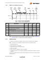
PRODUCT FEATURES
General Description
Features
The SMSC USB2640/USB2641 is a USB 2.0 compliant, HiSpeed hub for USB port expansion with an attached mass
storage class peripheral controller. The controller allows
read/write capability to popular flash media formats from the
following families:
xD-Picture CardTM (xD)1
Memory StickTM (MS)
Secure DigitalTM (SD)
MultiMediaCardTM (MMC)
The USB2640/USB2641 is a fully integrated, single chip
solution providing USB expansion and integrated flash card
media reader/writer capability of ultra high performance
operation. Average sustained transfer rates exceeding 35 MB/s
are possible if the media and host can support those rates.
Highlights
48-pin QFN package
Hub controller with internally connected ultra fast flash
media reader/writer and 2 exposed downstream ports for
external peripheral expansion
Flash media reader/writer employs multiplexed card
interfaces which are optimized for use with single card
insertion combo sockets
Hardware-controlled data flow architecture for all selfmapped media
Optional support for external firmware access via SPI
interface
Single chip flash media controller
Transaction translator (TT) in the hub supports operation of
FS and LS peripherals
Over 30 port configuration options
Customizable vendor ID, product ID, language ID
On board 24 MHz crystal driver circuit
Optional external 24 MHz clock input
GPIO configuration and polarity: Up to 8 GPIOs for special
function use
Internal card power FET
8051 8-bit microprocessor
Internal regulator for 1.8V core operation
Optimized pinout improves signal flow, easing
implementation and allowing for improved signal integrity
treatment
Optimized for low latency interrupt handling
Hub and flash media reader/writer configuration from a
single source: External I2C ROM or external SPI ROM
EEPROM update via USB
Please see the USB2640/USB2641 Software Release Notes
for additional software features
Applications
Printers
Desktop and Mobile PCs
Consumer A/V
Media Players/Viewers
Vista ReadyBoost™
1.xD-Picture Card not applicable to USB2641.
SMSC USB2640/USB2641
DATASHEET
Revision 2.0 (10-03-08)
Ultra Fast USB 2.0 Multi-Format Flash Media Controller/USB Hub Combo
ORDER NUMBER(S):
USB2640/USB2641-HZH for 48-PIN, QFN LEAD-FREE RoHS COMPLIANT PACKAGE
“XX” in the order number indicates the internal ROM firmware revision level.
Please contact your SMSC representative for more information.
80 ARKAY DRIVE, HAUPPAUGE, NY 11788 (631) 435-6000, FAX (631) 273-3123
Copyright © 2008 SMSC or its subsidiaries. All rights reserved.
Circuit diagrams and other information relating to SMSC products are included as a means of illustrating typical applications. Consequently, complete information sufficient for
construction purposes is not necessarily given. Although the information has been checked and is believed to be accurate, no responsibility is assumed for inaccuracies. SMSC
reserves the right to make changes to specifications and product descriptions at any time without notice. Contact your local SMSC sales office to obtain the latest specifications
before placing your product order. The provision of this information does not convey to the purchaser of the described semiconductor devices any licenses under any patent
rights or other intellectual property rights of SMSC or others. All sales are expressly conditional on your agreement to the terms and conditions of the most recently dated
version of SMSC's standard Terms of Sale Agreement dated before the date of your order (the "Terms of Sale Agreement"). The product may contain design defects or errors
known as anomalies which may cause the product's functions to deviate from published specifications. Anomaly sheets are available upon request. SMSC products are not
designed, intended, authorized or warranted for use in any life support or other application where product failure could cause or contribute to personal injury or severe property
damage. Any and all such uses without prior written approval of an Officer of SMSC and further testing and/or modification will be fully at the risk of the customer. Copies of
this document or other SMSC literature, as well as the Terms of Sale Agreement, may be obtained by visiting SMSC’s website at http://www.smsc.com. SMSC is a registered
trademark of Standard Microsystems Corporation (“SMSC”). Product names and company names are the trademarks of their respective holders.
SMSC DISCLAIMS AND EXCLUDES ANY AND ALL WARRANTIES, INCLUDING WITHOUT LIMITATION ANY AND ALL IMPLIED WARRANTIES OF MERCHANTABILITY,
FITNESS FOR A PARTICULAR PURPOSE, TITLE, AND AGAINST INFRINGEMENT AND THE LIKE, AND ANY AND ALL WARRANTIES ARISING FROM ANY COURSE
OF DEALING OR USAGE OF TRADE. IN NO EVENT SHALL SMSC BE LIABLE FOR ANY DIRECT, INCIDENTAL, INDIRECT, SPECIAL, PUNITIVE, OR CONSEQUENTIAL
DAMAGES; OR FOR LOST DATA, PROFITS, SAVINGS OR REVENUES OF ANY KIND; REGARDLESS OF THE FORM OF ACTION, WHETHER BASED ON CONTRACT;
TORT; NEGLIGENCE OF SMSC OR OTHERS; STRICT LIABILITY; BREACH OF WARRANTY; OR OTHERWISE; WHETHER OR NOT ANY REMEDY OF BUYER IS HELD
TO HAVE FAILED OF ITS ESSENTIAL PURPOSE, AND WHETHER OR NOT SMSC HAS BEEN ADVISED OF THE POSSIBILITY OF SUCH DAMAGES.
Revision 2.0 (10-03-08)
2
DATASHEET
SMSC USB2640/USB2641
Ultra Fast USB 2.0 Multi-Format Flash Media Controller/USB Hub Combo
Table of Contents
Chapter 1 Overview . . . . . . . . . . . . . . . . . . . . . . . . . . . . . . . . . . . . . . . . . . . . . . . . . . . . . . . . . . 7
1.1
1.2
Device Features . . . . . . . . . . . . . . . . . . . . . . . . . . . . . . . . . . . . . . . . . . . . . . . . . . . . . . . . . . . . . . . . 8
OEM Selectable Features. . . . . . . . . . . . . . . . . . . . . . . . . . . . . . . . . . . . . . . . . . . . . . . . . . . . . . . . . 9
Chapter 2 Acronyms . . . . . . . . . . . . . . . . . . . . . . . . . . . . . . . . . . . . . . . . . . . . . . . . . . . . . . . . 10
Chapter 3 Pin Configurations . . . . . . . . . . . . . . . . . . . . . . . . . . . . . . . . . . . . . . . . . . . . . . . . . 11
Chapter 4 Pin Tables . . . . . . . . . . . . . . . . . . . . . . . . . . . . . . . . . . . . . . . . . . . . . . . . . . . . . . . . 13
4.1
48-Pin Tables . . . . . . . . . . . . . . . . . . . . . . . . . . . . . . . . . . . . . . . . . . . . . . . . . . . . . . . . . . . . . . . . . 13
Chapter 5 Block Diagrams . . . . . . . . . . . . . . . . . . . . . . . . . . . . . . . . . . . . . . . . . . . . . . . . . . . 15
Chapter 6 Pin Descriptions . . . . . . . . . . . . . . . . . . . . . . . . . . . . . . . . . . . . . . . . . . . . . . . . . . . 17
6.1
6.2
6.3
6.4
USB2640/USB2641 Pin Descriptions . . . . . . . . . . . . . . . . . . . . . . . . . . . . . . . . . . . . . . . . . . . . . . .
Buffer Type Descriptions . . . . . . . . . . . . . . . . . . . . . . . . . . . . . . . . . . . . . . . . . . . . . . . . . . . . . . . .
Port Power Control . . . . . . . . . . . . . . . . . . . . . . . . . . . . . . . . . . . . . . . . . . . . . . . . . . . . . . . . . . . . .
ROM BOOT Sequence . . . . . . . . . . . . . . . . . . . . . . . . . . . . . . . . . . . . . . . . . . . . . . . . . . . . . . . . . .
17
23
24
26
Chapter 7 Configuration Options. . . . . . . . . . . . . . . . . . . . . . . . . . . . . . . . . . . . . . . . . . . . . . 27
7.1
7.2
7.3
7.4
7.5
Hub . . . . . . . . . . . . . . . . . . . . . . . . . . . . . . . . . . . . . . . . . . . . . . . . . . . . . . . . . . . . . . . . . . . . . . . . .
7.1.1
Hub Configuration Options . . . . . . . . . . . . . . . . . . . . . . . . . . . . . . . . . . . . . . . . . . . . . . .
7.1.2
VBus Detect. . . . . . . . . . . . . . . . . . . . . . . . . . . . . . . . . . . . . . . . . . . . . . . . . . . . . . . . . . .
Card Reader . . . . . . . . . . . . . . . . . . . . . . . . . . . . . . . . . . . . . . . . . . . . . . . . . . . . . . . . . . . . . . . . . .
System Configurations . . . . . . . . . . . . . . . . . . . . . . . . . . . . . . . . . . . . . . . . . . . . . . . . . . . . . . . . . .
7.3.1
EEPROM/SPI Interface . . . . . . . . . . . . . . . . . . . . . . . . . . . . . . . . . . . . . . . . . . . . . . . . . .
7.3.2
EEPROM Data Descriptor . . . . . . . . . . . . . . . . . . . . . . . . . . . . . . . . . . . . . . . . . . . . . . . .
7.3.3
LUN ID Strings. . . . . . . . . . . . . . . . . . . . . . . . . . . . . . . . . . . . . . . . . . . . . . . . . . . . . . . . .
7.3.4
I2C EEPROM . . . . . . . . . . . . . . . . . . . . . . . . . . . . . . . . . . . . . . . . . . . . . . . . . . . . . . . . . .
7.3.5
In-Circuit EEPROM Programming . . . . . . . . . . . . . . . . . . . . . . . . . . . . . . . . . . . . . . . . . .
Default Configuration Option: . . . . . . . . . . . . . . . . . . . . . . . . . . . . . . . . . . . . . . . . . . . . . . . . . . . . .
Reset . . . . . . . . . . . . . . . . . . . . . . . . . . . . . . . . . . . . . . . . . . . . . . . . . . . . . . . . . . . . . . . . . . . . . . .
7.5.1
Internal POR Hardware Reset . . . . . . . . . . . . . . . . . . . . . . . . . . . . . . . . . . . . . . . . . . . . .
7.5.2
External Hardware RESET_N . . . . . . . . . . . . . . . . . . . . . . . . . . . . . . . . . . . . . . . . . . . . .
7.5.3
USB Bus Reset . . . . . . . . . . . . . . . . . . . . . . . . . . . . . . . . . . . . . . . . . . . . . . . . . . . . . . . .
27
27
27
27
27
27
28
33
47
48
48
48
48
48
49
Chapter 8 Pin Reset States . . . . . . . . . . . . . . . . . . . . . . . . . . . . . . . . . . . . . . . . . . . . . . . . . . . 50
8.1
Pin Reset States . . . . . . . . . . . . . . . . . . . . . . . . . . . . . . . . . . . . . . . . . . . . . . . . . . . . . . . . . . . . . . . 50
Chapter 9 DC Parameters . . . . . . . . . . . . . . . . . . . . . . . . . . . . . . . . . . . . . . . . . . . . . . . . . . . . 54
9.1
9.2
9.3
9.4
Maximum Guaranteed Ratings . . . . . . . . . . . . . . . . . . . . . . . . . . . . . . . . . . . . . . . . . . . . . . . . . . . .
Operating Conditions . . . . . . . . . . . . . . . . . . . . . . . . . . . . . . . . . . . . . . . . . . . . . . . . . . . . . . . . . . .
DC Electrical Characteristics . . . . . . . . . . . . . . . . . . . . . . . . . . . . . . . . . . . . . . . . . . . . . . . . . . . . .
Capacitance . . . . . . . . . . . . . . . . . . . . . . . . . . . . . . . . . . . . . . . . . . . . . . . . . . . . . . . . . . . . . . . . . .
54
55
55
57
Chapter 10 AC Specifications . . . . . . . . . . . . . . . . . . . . . . . . . . . . . . . . . . . . . . . . . . . . . . . . . . 58
10.1
Oscillator/Clock. . . . . . . . . . . . . . . . . . . . . . . . . . . . . . . . . . . . . . . . . . . . . . . . . . . . . . . . . . . . . . . . 58
Chapter 11 Package Outline . . . . . . . . . . . . . . . . . . . . . . . . . . . . . . . . . . . . . . . . . . . . . . . . . . . 59
SMSC USB2640/USB2641
3
DATASHEET
Revision 2.0 (10-03-08)
Ultra Fast USB 2.0 Multi-Format Flash Media Controller/USB Hub Combo
Chapter 12 GPIO Usage . . . . . . . . . . . . . . . . . . . . . . . . . . . . . . . . . . . . . . . . . . . . . . . . . . . . . . 60
Revision 2.0 (10-03-08)
4
DATASHEET
SMSC USB2640/USB2641
Ultra Fast USB 2.0 Multi-Format Flash Media Controller/USB Hub Combo
List of Tables
Table 4.1 USB2640 48-Pin Table . . . . . . . . . . . . . . . . . . . . . . . . . . . . . . . . . . . . . . . . . . . . . . . . . . . . . .
Table 4.2 USB2641 48-Pin Table . . . . . . . . . . . . . . . . . . . . . . . . . . . . . . . . . . . . . . . . . . . . . . . . . . . . . .
Table 6.1 USB2640/USB2641 Pin Descriptions . . . . . . . . . . . . . . . . . . . . . . . . . . . . . . . . . . . . . . . . . . .
Table 6.2 USB2640/USB2641 Buffer Type Descriptions. . . . . . . . . . . . . . . . . . . . . . . . . . . . . . . . . . . . .
Table 7.1 Internal Flash Media Controller Configurations . . . . . . . . . . . . . . . . . . . . . . . . . . . . . . . . . . . .
Table 7.2 Hub Controller Configurations . . . . . . . . . . . . . . . . . . . . . . . . . . . . . . . . . . . . . . . . . . . . . . . . .
Table 7.3 Other Internal Configurations. . . . . . . . . . . . . . . . . . . . . . . . . . . . . . . . . . . . . . . . . . . . . . . . . .
Table 7.4 FET Configuration . . . . . . . . . . . . . . . . . . . . . . . . . . . . . . . . . . . . . . . . . . . . . . . . . . . . . . . . . .
Table 7.5 Port Remap Register for Ports 1 & 2 . . . . . . . . . . . . . . . . . . . . . . . . . . . . . . . . . . . . . . . . . . . .
Table 7.6 Port Remap Register for Port 3 . . . . . . . . . . . . . . . . . . . . . . . . . . . . . . . . . . . . . . . . . . . . . . . .
Table 7.7 Reset_N Timing for EEPROM Mode . . . . . . . . . . . . . . . . . . . . . . . . . . . . . . . . . . . . . . . . . . . .
Table 8.1 Legend for Pin Reset States Table . . . . . . . . . . . . . . . . . . . . . . . . . . . . . . . . . . . . . . . . . . . . .
Table 8.2 USB2640 Pin Reset States . . . . . . . . . . . . . . . . . . . . . . . . . . . . . . . . . . . . . . . . . . . . . . . . . . .
Table 8.3 USB2641 Pin Reset States . . . . . . . . . . . . . . . . . . . . . . . . . . . . . . . . . . . . . . . . . . . . . . . . . . .
Table 9.1 Pin Capacitance. . . . . . . . . . . . . . . . . . . . . . . . . . . . . . . . . . . . . . . . . . . . . . . . . . . . . . . . . . . .
Table 12.1 USB2640/USB2641 GPIO Usage . . . . . . . . . . . . . . . . . . . . . . . . . . . . . . . . . . . . . . . . . . . . . .
SMSC USB2640/USB2641
5
DATASHEET
13
14
17
23
28
29
30
33
45
46
49
50
50
52
57
60
Revision 2.0 (10-03-08)
Ultra Fast USB 2.0 Multi-Format Flash Media Controller/USB Hub Combo
List of Figures
Figure 3.1
Figure 3.2
Figure 5.1
Figure 5.2
Figure 6.1
Figure 6.2
Figure 6.3
Figure 6.4
Figure 6.5
Figure 7.1
Figure 8.1
Figure 9.1
Figure 10.1
Figure 10.2
Figure 11.1
USB2640 48-Pin QFN . . . . . . . . . . . . . . . . . . . . . . . . . . . . . . . . . . . . . . . . . . . . . . . . . . . . . .
USB2641 48-Pin QFN . . . . . . . . . . . . . . . . . . . . . . . . . . . . . . . . . . . . . . . . . . . . . . . . . . . . . .
USB2640 Block Diagram . . . . . . . . . . . . . . . . . . . . . . . . . . . . . . . . . . . . . . . . . . . . . . . . . . . .
USB2641 Block Diagram . . . . . . . . . . . . . . . . . . . . . . . . . . . . . . . . . . . . . . . . . . . . . . . . . . . .
Port Power Control with USB Power Switch . . . . . . . . . . . . . . . . . . . . . . . . . . . . . . . . . . . . .
Port Power Control with Single Poly Fuse and Multiple Loads . . . . . . . . . . . . . . . . . . . . . . .
Port Power with Ganged Control with Poly Fuse . . . . . . . . . . . . . . . . . . . . . . . . . . . . . . . . . .
USB2640/USB2641 SPI ROM Connection . . . . . . . . . . . . . . . . . . . . . . . . . . . . . . . . . . . . . .
USB2640/USB2641 I2C Connection . . . . . . . . . . . . . . . . . . . . . . . . . . . . . . . . . . . . . . . . . . .
Reset_N Timing for EEPROM Mode . . . . . . . . . . . . . . . . . . . . . . . . . . . . . . . . . . . . . . . . . . .
Pin Reset States . . . . . . . . . . . . . . . . . . . . . . . . . . . . . . . . . . . . . . . . . . . . . . . . . . . . . . . . . .
Supply Rise Time Models . . . . . . . . . . . . . . . . . . . . . . . . . . . . . . . . . . . . . . . . . . . . . . . . . . .
Typical Crystal Circuit . . . . . . . . . . . . . . . . . . . . . . . . . . . . . . . . . . . . . . . . . . . . . . . . . . . . . .
Formula to find value of C1 and C21 . . . . . . . . . . . . . . . . . . . . . . . . . . . . . . . . . . . . . . . . . . .
USB2640/USB2641 48-Pin QFN . . . . . . . . . . . . . . . . . . . . . . . . . . . . . . . . . . . . . . . . . . . . . .
Revision 2.0 (10-03-08)
6
DATASHEET
11
12
15
16
24
25
25
26
26
49
50
54
58
58
59
SMSC USB2640/USB2641
Ultra Fast USB 2.0 Multi-Format Flash Media Controller/USB Hub Combo
Chapter 1 Overview
The SMSC USB2640/USB2641 is an integrated USB 2.0 compliant, Hi-Speed hub for USB port
expansion with an attached bulk only mass storage class peripheral controller. This multi-format flash
media controller and USB Hub Combo features 3 downstream ports: one port is dedicated to an
internally connected ultra fast flash media reader/writer and 2 exposed downstream ports are
available for external peripheral expansion.
The SMSC USB2640/USB2641 is an ultra fast, OEM configurable, hub controller IC with 3
downstream ports for embedded USB solutions. The USB2640/USB2641 will attach to an upstream
port as a Full-Speed Hub or as a Full-/Hi-Speed Hub. The hub supports Low-Speed, Full-Speed, and
Hi-Speed (if operating as a Hi-Speed Hub) downstream devices on all of the enabled downstream
ports.
All required resistors on the USB ports are integrated into the hub. This includes all series
termination resistors on D+ and D– pins and all required pull-down and pull-up resistors on D+ and
D– pins. The over-current sense inputs for the downstream facing ports have internal pull-up
resistors.
The USB2640/USB2641 includes over 30 programmable features including:
PortMap (also referred to as port remap) which provides flexible port mapping and disable
sequences. The downstream ports of a USB2640/USB2641 hub can be reordered or disabled in any
sequence to support multiple platform designs with minimum effort. For any port that is disabled, the
USB2640/USB2641 automatically reorders the remaining ports to match the USB host controller’s
port numbering scheme.
PortSwap which adds per-port programmability to USB differential-pair pin locations. PortSwap
allows direct alignment of USB signals (D+/D-) to connectors avoiding uneven trace length or
crossing of the USB differential signals on the PCB.
PHYBoost which enables four programmable levels of USB signal drive strength in downstream port
transceivers. PHYBoost attempts to restore USB signal integrity that has been compromised by
system level variables such as poor PCB layout, long cables, etc.
SMSC USB2640/USB2641
7
DATASHEET
Revision 2.0 (10-03-08)
Ultra Fast USB 2.0 Multi-Format Flash Media Controller/USB Hub Combo
1.1
Device Features
Hardware Features
Single chip flash media controller
Transaction translator (TT) in the hub supports operation of FS and LS peripherals
Full power management with individual or ganged power control of each downstream port
Optional support for external firmware access via SPI interface
- 30 MHz or 60 MHz operation support
- Single bit or dual bit mode support
- Mode 0 or mode 3 SPI support
Memory Stick Specification 1.43
Memory Stick Pro Format Specification 1.02
Memory Stick Pro-HG Duo Format Specification 1.01 compliant
- Memory Stick, MS Duo, HS-MS, MS Pro-HG, MS Pro
xD-Picture Card 1.2 compliant
Secure Digital 2.0 / MultiMediaCard Specification 4.3 compliant
- SD 2.0, HS-SD, HC-SD
- TransFlash™ and reduced form factor media
- 1/4/8 bit MMC 4.2
SDIO and MMC streaming mode support
On board 24 MHz crystal driver circuit
Optional external 24 MHz clock input. Must be used with an external resistor divider to provide a
1.8V signal.
GPIO configuration and polarity
- Up to 8 GPIOs for special function use: LED indicators, button inputs, power control to memory
devices, etc. The number of actual GPIO’s depends on the implementation configuration used.
- One GPIO with up to 200 mA drive.
Internal card power FET
-Up to 200 mA operation available
-"Fold-back" short circuit current protected
8051 8-bit microprocessor
- 60 MHz - single cycle execution
- 64 KB ROM; 9 KB RAM
Internal Regulator for 1.8V core operation
Optimized pinout improves signal flow, easing implementation and allowing for improved signal
integrity treatment
Software Features
Optimized for low latency interrupt handling
Hub and flash media reader/writer configuration from a single source: External I2C ROM or external
SPI ROM
EEPROM update via USB
Please see the USB2640/USB2641 Software Release Notes for additional software features
Revision 2.0 (10-03-08)
8
DATASHEET
SMSC USB2640/USB2641
Ultra Fast USB 2.0 Multi-Format Flash Media Controller/USB Hub Combo
1.2
OEM Selectable Features
Hub
A default configuration is available in the USB2640/USB2641 following a reset. The
USB2640/USB2641 may also be configured by an external I2C EEPROM or via external SPI flash.
The USB2640/USB2641 supports several OEM selectable features:
Compound device support (port is permanently hardwired to a downstream USB peripheral device),
on a port-by-port basis.
Select over-current sensing and port power control on an individual (port-by-port) or ganged (all
ports together) basis to match the OEM’s choice of circuit board component selection.
Port power control and over-current detection/delay features
Configure the delay time for filtering the over-current sense inputs.
Configure the delay time for turning on downstream port power.
Bus- or self-powered selection
Hub port disable or non-removable configurations
Port signal swapping for easier board layout
Flexible port mapping and disable sequence. Ports can be disabled/reordered in any sequence to
support multiple platforms with a single design. The hub will automatically reorder the remaining
ports to match the host controller's numbering scheme.
Programmable USB differential-pair pin location.
- Eases PCB layout by aligning USB signal lines directly to connectors
Programmable USB signal drive strength. Recover USB signal integrity due to compromised
system environments using 4 levels of signal drive strength.
Indicate the maximum current that the 2-port hub consumes from the USB upstream port.
Indicate the maximum current required for the hub controller.
Flash Media Controller
Customize vendor ID, product ID, and device ID.
12-hex digit (max) serial number string
Customizable vendor specific data by optional use of external serial EEPROM
28-character manufacturer ID and product string for flash media reader/writer
LED blink interval or duration
SMSC USB2640/USB2641
9
DATASHEET
Revision 2.0 (10-03-08)
Ultra Fast USB 2.0 Multi-Format Flash Media Controller/USB Hub Combo
Chapter 2 Acronyms
FM: Flash Media
FMC: Flash Media Controller
FS: Full-speed Device
LS: Low-speed Device
HS: Hi-speed Device
I2C®: Inter-Integrated Circuit1
MMC: MultiMediaCard
MS: Memory Stick
MSC: Memory Stick Controller
OCS: Over-current Sense
SD: Secure Digital
SDC: Secure Digital Controller
UCHAR: Unsigned Character
UINT: Unsigned Integer
xD: xD-Picture Card
Standard Microsystems is a registered trademark and SMSC is a trademark of Standard Microsystems Corporation. Other product
and company names are trademarks or registered trademarks of their respective holders.
*Note: In order to develop, make, use, or sell readers and/or other products using or incorporating any of the SMSC devices made
the subject of this document or to use related SMSC software programs, technical information and licenses under patent and other
intellectual property rights from or through various persons or entities, including without limitation media standard companies,
forums, and associations, and other patent holders may be required. These media standard companies, forums, and associations
include without limitation the following: Sony Corporation (Memory Stick, Memory Stick Pro); SD3 LLC (Secure Digital); MultiMedia
Card Association (MultiMediaCard); the SSFDC Forum (SmartMedia); the Compact Flash Association (Compact Flash); and Fuji
Photo Film Co., Ltd., Olympus Optical Co., Ltd., and Toshiba Corporation (xD-Picture Card). SMSC does not make such licenses
or technical information available; does not promise or represent that any such licenses or technical information will actually be
obtainable from or through the various persons or entities (including the media standard companies, forums, and associations), or
with respect to the terms under which they may be made available; and is not responsible for the accuracy or sufficiency of, or
otherwise with respect to, any such technical information.
SMSC's obligations (if any) under the Terms of Sale Agreement, or any other agreement with any customer, or otherwise, with
respect to infringement, including without limitation any obligations to defend or settle claims, to reimburse for costs, or to pay
damages, shall not apply to any of the devices made the subject of this document or any software programs related to any of such
devices, or to any combinations involving any of them, with respect to infringement or claimed infringement of any existing or future
patents related to solid state disk or other flash memory technology or applications ("Solid State Disk Patents"). By making any
purchase of any of the devices made the subject of this document, the customer represents, warrants, and agrees that it has
obtained all necessary licenses under then-existing Solid State Disk Patents for the manufacture, use and sale of solid state disk
and other flash memory products and that the customer will timely obtain at no cost or expense to SMSC all necessary licenses
under Solid State Disk Patents; that the manufacture and testing by or for SMSC of the units of any of the devices made the subject
of this document which may be sold to the customer, and any sale by SMSC of such units to the customer, are valid exercises of
the customer's rights and licenses under such Solid State Disk Patents; that SMSC shall have no obligation for royalties or otherwise
under any Solid State Disk Patents by reason of any such manufacture, use, or sale of such units; and that SMSC shall have no
obligation for any costs or expenses related to the customer's obtaining or having obtained rights or licenses under any Solid State
Disk Patents.
SMSC MAKES NO WARRANTIES, EXPRESS, IMPLIED, OR STATUTORY, IN REGARD TO INFRINGEMENT OR OTHER
VIOLATION OF INTELLECTUAL PROPERTY RIGHTS. SMSC DISCLAIMS AND EXCLUDES ANY AND ALL WARRANTIES
AGAINST INFRINGEMENT AND THE LIKE.
No license is granted by SMSC expressly, by implication, by estoppel or otherwise, under any patent, trademark, copyright, mask
work right, trade secret, or other intellectual property right.
**To obtain this software program the appropriate SMSC Software License Agreement must be executed and in effect. Forms of
these Software License Agreements may be obtained by contacting SMSC.
1.I2C is a registered trademark of Philips Corporation.
Revision 2.0 (10-03-08)
10
DATASHEET
SMSC USB2640/USB2641
Ultra Fast USB 2.0 Multi-Format Flash Media Controller/USB Hub Combo
GPIO2 / RXD
GPIO10 (CRD_PWR)
VDD33
xD_D5 / SD_D2
xD_D6 / SD_D3 / MS_D3
GPIO12 / MS_INS
xD_D7 / SD_D4 / MS_D2
GPIO14 / xD_nCD
xD_nB/R
xD_nRE
xD_nCE
VDD33
36
35
34
33
32
31
30
29
28
27
26
25
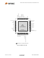
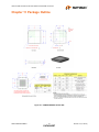
Chapter 3 Pin Configurations
GPIO1 / LED1 / TXD
37
24
xD_CLE / SD_CMD / MS_D0
nRESET
38
23
xD_ALE / SD_D5 / MS_D1
VBUS_DET
39
22
xD_nWE
TEST
40
21
xD_nWP / SD_CLK / MS_BS
VDDA33
41
20
xD_D0 / SD_D6 / MS_D7
USB+
42
19
xD_D1 / SD_D7 / MS_D6
USB-
43
18
xD_D2 / SD_D0 / MS_D4
XTAL2
44
17
xD_D3 / SD_D1 / MS_D5
XTAL1 (CLKIN)
45
16
VDD33
VDD18PLL
46
15
VDD18
RBIAS
47
14
GPIO15 / SD_nCD
VDDA33
48
13
xD_D4 / GPIO6 / SD_WP / MS_SCLK
SMSC
USB2640
(Top View QFN-48)
10
11
12
SPI_DI
VDD33
9
SPI_CLK / GPIO4 / SCL
SPI_DO / GPIO5 / SDA / SPI_SPD_SEL
8
SPI_CE_N
5
VDDA33
7
4
USBDN_DP3
6
3
USBDN_DM3
PRTCTL3
2
USBDN_DP2
PRTCTL2
1
USBDN_DM2
Thermal Slug
(must be connected to VSS)
Indicates pins on the bottom of the device .
Figure 3.1 USB2640 48-Pin QFN
SMSC USB2640/USB2641
11
DATASHEET
Revision 2.0 (10-03-08)
GPIO2 / RXD
GPIO10 (CRD_PWR)
VDD33
SD_D2
SD_D3 / MS_D3
GPIO12 / MS_INS
SD_D4 / MS_D2
GPIO14
NC
NC
NC
VDD33
36
35
34
33
32
31
30
29
28
27
26
25
Ultra Fast USB 2.0 Multi-Format Flash Media Controller/USB Hub Combo
GPIO1 / LED1 / TXD
37
24
SD_CMD / MS_D0
nRESET
38
23
SD_D5 / MS_D1
VBUS_DET
39
22
NC
TEST
40
21
SD_CLK / MS_BS
VDDA33
41
20
SD_D6 / MS_D7
USB+
42
19
SD_D7 / MS_D6
USB-
43
18
SD_D0 / MS_D4
XTAL2
44
17
SD_D1 / MS_D5
XTAL1 (CLKIN)
45
16
VDD33
VDD18PLL
46
15
VDD18
RBIAS
47
14
GPIO15 / SD_nCD
VDDA33
48
13
GPIO6 / SD_WP / MS_SCLK
SMSC
USB2641
(Top View QFN-48)
10
11
12
SPI_DI
VDD33
9
SPI_CLK / GPIO4 / SCL
SPI_DO / GPIO5 / SDA / SPI_SPD_SEL
8
SPI_CE_N
5
VDDA33
7
4
USBDN_DP3
PRTCTL3
3
6
2
USBDN_DP2
USBDN_DM3
PRTCTL2
1
USBDN_DM2
Thermal Slug
(must be connected to VSS)
Indicates pins on the bottom of the device .
Figure 3.2 USB2641 48-Pin QFN
Revision 2.0 (10-03-08)
12
DATASHEET
SMSC USB2640/USB2641
Ultra Fast USB 2.0 Multi-Format Flash Media Controller/USB Hub Combo
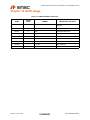
Chapter 4 Pin Tables
4.1
48-Pin Tables
Table 4.1 USB2640 48-Pin Table
xD (Only in USB2640) / SECURE DIGITAL / MEMORY STICK INTERFACE (18 PINS)
xD_D3 /
SD_D1 /
MS_D5
xD_D2 /
SD_D0 /
MS_D4
xD_D1 /
SD_D7 /
MS_D6
xD_D0 /
SD_D6 /
MS_D7
xD_nWP /
SD_CLK /
MS_BS
xD_ALE /
SD_D5 /
MS_D1
xD_CLE /
SD_CMD /
MS_D0
xD_D7 /
SD_D4 /
MS_D2
xD_D6 /
SD_D3 /
MS_D3
xD_D5 / SD_D2
xD_nRE
xD_nWE
xD_D4 /
GPIO6 / SD_WP /
MS_SCLK
xD_nB/R
xD_nCE
GPIO12 / MS_INS
GPIO14 / xD_nCD
GPIO15 / SD_nCD
USB INTERFACE (9 PINS)
USB+
USB-
XTAL1 (CLKIN)
RBIAS
(3) VDDA33
VDD18PLL
XTAL2
2-PORT USB INTERFACE (7 PINS)
USBDN_DP2
USBDN_DM2
PRTCTL2
USBDN_DP3
USBDN_DM3
VBUS_DET
PRTCTL3
SPI INTERFACE (4 PINS)
SPI_CE_N
SPI_DO / GPIO5 /
SDA / SPI_SPD_SEL
SPI_CLK / GPIO4 / SCL
SPI_DI
MISC (5 PINS)
nRESET
TEST
GPIO1 / LED1 / TXD
GPIO2 / RXD
GPIO10 (CRD_PWR)
DIGITAL POWER (5 PINS)
(4) VDD33
VDD18
TOTAL 48
SMSC USB2640/USB2641
13
DATASHEET
Revision 2.0 (10-03-08)
Ultra Fast USB 2.0 Multi-Format Flash Media Controller/USB Hub Combo
Table 4.2 USB2641 48-Pin Table
SECURE DIGITAL / MEMORY STICKINTERFACE (14 PINS)
SD_D1 /
MS_D5
SD_D0 /
MS_D4
SD_D7 /
MS_D6
SD_D6 /
MS_D7
SD_CLK /
MS_BS
SD_D5 /
MS_D1
SD_CMD /
MS_D0
SD_D4 /
MS_D2
SD_D3 /
MS_D3
SD_D2
GPIO12 / MS_INS
GPIO14
GPIO6 / SD_WP /
MS_SCLK
GPIO15 / SD_nCD
USB INTERFACE (9 PINS)
USB+
USB-
XTAL1 (CLKIN)
RBIAS
(3) VDDA33
VDD18PLL
XTAL2
2-PORT USB INTERFACE (7 PINS)
USBDN_DP2
USBDN_DM2
PRTCTL2
USBDN_DP3
USBDN_DM3
VBUS_DET
PRTCTL3
SPI INTERFACE (4 PINS)
SPI_CE_N
SPI_DO / GPIO5 /
SDA / SPI_SPD_SEL
SPI_CLK / GPIO4 / SCL
SPI_DI
MISC (5 PINS)
nRESET
TEST
GPIO1 / LED1 / TXD
GPIO2 / RXD
GPIO10
(CRD_PWR)
DIGITAL POWER, NO CONNECTS (9 PINS)
(4) VDD33
VDD18
(4) NC
TOTAL 48
Revision 2.0 (10-03-08)
14
DATASHEET
SMSC USB2640/USB2641
SMSC USB2640/USB2641
DATASHEET
15
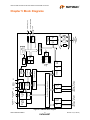
USB Data
Downstream
PHY
3.3V
Transaction
Translator
Serial
Interface
Engine
1.8V Reg
PLL
24 MHz
Crystal
USB Data OC Sense/
Downstream Pwr Switch
PHY
Port #2
OC
Sense
Switch
Driver
Routing & Port Re-Ordering Logic
OC Sense/
Pwr Switch
Port #3
OC
Sense
Switch
Driver
Upstream
PHY
Bus-Power
Detect/VBUS
Pulse
Repeater
Upstream USB
Data
To Upstream
VBUS
1.8V
BRIDGE
Port Controller
Controller
Serial
Interface
SIE
CTL
3K
total
BUS
INTFC
ADDR
MAP
EP2 RX
EP2 TX
RAM
EP0 TX
EP0 RX
ROM
64K
RAM
6K
SFR
RAM
BUS
INTFC
GPIOs
PWR_FET0
SPI
xD
XDATA BRIDGE
+ BUS ARBITER
SD/
MMC
FMI
FMDU
CTL
Flash Media
Cards
(require Combo
socket)
MS
BUS
INTFC
AUTO_CBW
PROC
Program Memory I/O Bus
8051
PROCESSOR
6 pins
GPIO10 (CRD_PWR)
SPI / GPIO (2 pins)
Ultra Fast USB 2.0 Multi-Format Flash Media Controller/USB Hub Combo
Chapter 5 Block Diagrams
Figure 5.1 USB2640 Block Diagram
Revision 2.0 (10-03-08)
Revision 2.0 (10-03-08)
DATASHEET
16
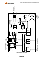
USB Data
Downstream
PHY
3.3V
Transaction
Translator
Serial
Interface
Engine
1.8V Reg
PLL
24 MHz
Crystal
USB Data OC Sense/
Downstream Pwr Switch
PHY
Port #2
OC
Sense
Switch
Driver
Routing & Port Re-Ordering Logic
OC Sense/
Pwr Switch
Port #3
OC
Sense
Switch
Driver
Upstream
PHY
Bus-Power
Detect/VBUS
Pulse
Repeater
Upstream USB
Data
To Upstream
VBUS
1.8V
BRIDGE
Port Controller
Controller
Serial
Interface
SIE
CTL
3K
total
BUS
INTFC
ADDR
MAP
EP2 RX
EP2 TX
RAM
EP0 TX
EP0 RX
ROM
64K
RAM
6K
SFR
RAM
BUS
INTFC
GPIOs
PWR_FET0
SPI
Flash Media
Cards
(require Combo
socket)
SD/
MMC
FMI
FMDU
CTL
AUTO_CBW
PROC
BUS
INTFC
MS
XDATA BRIDGE
+ BUS ARBITER
Program Memory I/O Bus
8051
PROCESSOR
6 pins
GPIO10 (CRD_PWR)
SPI / GPIO (2 pins)
Ultra Fast USB 2.0 Multi-Format Flash Media Controller/USB Hub Combo
Figure 5.2 USB2641 Block Diagram
SMSC USB2640/USB2641
Ultra Fast USB 2.0 Multi-Format Flash Media Controller/USB Hub Combo
Chapter 6 Pin Descriptions
This section provides a detailed description of each signal. The signals are arranged in functional
groups according to their associated interface.
The “n” symbol in the signal name indicates that the active, or asserted, state occurs when the signal
is at a low voltage level. When “n” is not present before the signal name, the signal is asserted when
at the high voltage level.
The terms assertion and negation are used exclusively. This is done to avoid confusion when working
with a mixture of “active low” and “active high” signal. The term assert, or assertion, indicates that a
signal is active, independent of whether that level is represented by a high or low voltage. The term
negate, or negation, indicates that a signal is inactive.
6.1
USB2640/USB2641 Pin Descriptions
Table 6.1 USB2640/USB2641 Pin Descriptions
NAME
SYMBOL
48-PIN
QFN
BUFFER
TYPE
DESCRIPTION
xD INTERFACE (APPLIES ONLY TO USB2640)
xD Write Protect
xD_nWP
21
O12PD
This pin is an active low write protect signal for the
xD device.
This pin has a weak pull-down resistor that is
permanently enabled.
xD Address
Strobe
xD_ALE
23
O12PD
This pin is an active high Address Latch Enable
signal for the xD device.
This pin has a weak pull-down resistor that is
permanently enabled.
xD Command
Strobe
xD_CLE
24
O12PD
This pin is an active high Command Latch Enable
signal for the xD device.
This pin has a weak pull-down resistor that is
permanently enabled.
xD Data 7-0
xD Read Enable
xD_D[7:0]
xD_nRE
30
32
33
13
17
18
19
20
I/O12PD
27
O12PU
These pins are the bi-directional data signal
xD_D7 - xD_D0.
The bi-directional data signal has an internal weak
pull-down resistor.
This pin is an active low read strobe signal for the
xD device.
When using the internal FET, this pin has an
internal weak pull-up resistor that is tied to the
output of the internal Power FET and is controlled
by the xD_PU bit of the xDC_CTL register.
If an external FET is used (Internal FET is
disabled), then the internal pull-up is not available
(external pull-ups must be used).
SMSC USB2640/USB2641
17
DATASHEET
Revision 2.0 (10-03-08)
Ultra Fast USB 2.0 Multi-Format Flash Media Controller/USB Hub Combo
Table 6.1 USB2640/USB2641 Pin Descriptions (continued)
NAME
SYMBOL
48-PIN
QFN
BUFFER
TYPE
xD Write Enable
xD_nWE
22
O12PU
DESCRIPTION
This pin is an active low write strobe signal for the
xD device.
When using the internal FET, this pin has an
internal weak pull-up resistor that is tied to the
output of the internal Power FET, and is controlled
by the xD_PU bit of the xDC_CTL register.
If an external FET is used (Internal FET is
disabled), then the internal pull-up is not available
(external pull-ups must be used).
xD Busy or Data
Ready
xD_nB/R
28
IPU
This pin is connected to the BSY/RDY pin of the
xD device.
When using the internal FET, this pin has an
internal weak pull-up resistor that is tied to the
output of the internal Power FET, and is controlled
by the xD_PU bit of the xDC_CTL register.
If an external FET is used (Internal FET is
disabled), then the internal pull-up is not available
(external pull-ups must be used).
xD Chip Enable
xD_nCE
26
O12PU
This pin is an active low chip enable signal for the
xD device.
When using the internal FET, this pin has an
internal weak pull-up resistor that is tied to the
output of the internal Power FET, and is controlled
by the xD_PU bit of the xDC_CTL register.
If an external FET is used (Internal FET is
disabled), then the internal pull-up is not available
(external pull-ups must be used).
xD Card
Detection GPIO
GPIO14 /
xD_nCD
29
I/O12
GPIO: This general purpose pin may be used
either as input, edge sensitive interrupt input, or
output.
xD_nCD: This is a GPIO designated as the xDPicture Card detection pin.
MEMORY STICK INTERFACE
MS Bus State
MS_BS
21
O12
This pin is connected to the BS pin of the MS
device.
It is used to control the Bus States 0, 1, 2, and 3
(BS0, BS1, and BS3) of the MS device.
MS Card
Insertion GPIO
GPIO12 /
MS_INS
31
IPU
GPIO: This general purpose pin may be used
either as input, edge sensitive interrupt input, or
output.
MS_INS: This is a GPIO designated as the
Memory Stick card detection Pin.
MS System CLK
MS_SCLK
13
O12
This pin is an output clock signal to the MS device.
The clock frequency is software configurable.
Revision 2.0 (10-03-08)
18
DATASHEET
SMSC USB2640/USB2641
Ultra Fast USB 2.0 Multi-Format Flash Media Controller/USB Hub Combo
Table 6.1 USB2640/USB2641 Pin Descriptions (continued)
NAME
SYMBOL
MS System Data
In/Out
MS_D[7:0]
48-PIN
QFN
BUFFER
TYPE
20
19
17
18
32
30
23
24
I/O12PD
DESCRIPTION
These pins are the bi-directional data signals for
the MS device. In serial mode, the most significant
bit (MSB) of each byte is transmitted first by either
MSC or MS device on MS_D0.
MS_D0, MS_D2, and MS_D3 have weak pulldown resistors. MS_D1 has a pull down resistor if
in parallel mode, otherwise it is disabled. In 4 or 8
bit parallel modes, there is a weak pull-down
resistor on all MS_D7 - MS_D0 signals.
The resistors are controlled by MSC_SYSTE_0,
MSC_MODE_CTL and MSC_PRO_HG registers.
SECURE DIGITAL / MULTIMEDIACARD INTERFACE
SD Data 7-0
SD_D[7:0]
SD Clock
SD_CLK
19
20
23
30
32
33
17
18
I/O12PU
21
O12
These are the bi-directional data signals SD_D0SD_D7.
SD_D0 - SD_D7 have weak pull-up resistors.
This is an output clock signal to SD/MMC device.
The clock frequency is software configurable.
SD Command
SD_CMD
24
I/O12PU
This is a bi-directional signal that connects to the
CMD signal of the SD/MMC device.
The bi-directional signal should have an internal
weak pull-up resistor.
The pull-up register can be controlled by:
SD_MMC_INTF_EN bit of SDC_MODE CTL.
SD Write
Protected GPIO
GPIO6 /
SD_WP
13
I/O12
GPIO: This general purpose pin may be used
either as input, edge sensitive interrupt input, or
output.
SD_WP: This is a GPIO designated as the Secure
Digital card mechanical write detect pin.
SD Card Detect
GPIO
GPIO15 /
SD_nCD
14
I/O12
GPIO:This general purpose pin may be used
either as input, edge sensitive interrupt input, or
output.
SD_nCD: This is a GPIO designated as the
Secure Digital card detection pin.
USB INTERFACE
USB Bus Data
USBUSB+
43
42
I/O-U
These pins connect to the upstream USB bus data
signals.
USB Bus Data
USBDN_DM
[3:2]
USBDN_DP
[3:2]
3
1
4
2
I/O-U
These pins connect to the downstream USB bus
data signals.
SMSC USB2640/USB2641
19
DATASHEET
Revision 2.0 (10-03-08)
Ultra Fast USB 2.0 Multi-Format Flash Media Controller/USB Hub Combo
Table 6.1 USB2640/USB2641 Pin Descriptions (continued)
NAME
USB Power
Enable
SYMBOL
PRTCTL[3:2]
48-PIN
QFN
BUFFER
TYPE
7
6
I/OD12PU
DESCRIPTION
As an output, these pins enables power
downstream USB peripheral devices. See Section
6.3, "Port Power Control" for diagram and usage
instructions.
As an input, when the power is enabled, these
pins monitor the over-current condition. When an
over-current condition is detected, the pins turn the
power off.
Detect Upstream
VBUS Power
VBUS_DET
39
I
Detects the state of upstream VBUS power. The
Hub monitors VBUS_DET to determine when to
assert the internal D+ pull-up resistor (signaling a
connect event).
When designing a detachable hub, connect this
pin to the VBUS power pin of the USB port that is
upstream of the Hub.
For self-powered applications with a permanently
attached host, this pin should be pulled up,
typically to VDD33.
VBUS is a 3.3V input. A resistor divider must be
used when connecting to 5V USB power.
USB Transceiver
Bias
RBIAS
47
I-R
A 12.0 kΩ , ±1.0% resistor is attached from VSSA
to this pin in order to set the transceiver's internal
bias currents.
Crystal
Input/External
Clock Input
XTAL1
(CLKIN)
45
ICLKx
24 MHz Crystal or external clock input.
This pin can be connected to one terminal of the
crystal or it can be connected to an external
24MHz clock when a crystal is not used.
XTAL2
44
OCLKx
24 MHz Crystal.
This is the other terminal of the crystal, or it is left
open when an external clock source is used to
drive XTAL1(CLKIN).
Crystal
Output
Note:
1.8V PLL Power
Bypass
3.3V Analog
Power
Do not use it to drive any external
circuitry other than the crystal circuit.
VDD18PLL
46
This pin is the 1.8V Power bypass for the PLL.
This requires an external bypass capacitor of 1.0
μF minimum.
VDDA33
5
41
48
3.3V Analog Power
SPI INTERFACE
SPI Chip Enable
SPI_CE_N
8
O12
This is the active low chip enable output.
If the SPI interface is enabled, this pin must be
driven high in power down states.
Revision 2.0 (10-03-08)
20
DATASHEET
SMSC USB2640/USB2641
Ultra Fast USB 2.0 Multi-Format Flash Media Controller/USB Hub Combo
Table 6.1 USB2640/USB2641 Pin Descriptions (continued)
NAME
SYMBOL
SPI Clock
SPI_CLK /
GPIO4 /
SCL
48-PIN
QFN
BUFFER
TYPE
9
I/O12
DESCRIPTION
SPI_CLK: This is the SPI clock out to the serial
ROM. See Section 6.4, "ROM BOOT Sequence"
for diagram and usage instructions.
When the SPI interface is disabled, by setting the
SPI_DISABLE bit in the UTIL_CONFIG1 register,
this pin becomes GPIO4.
During reset, this pin must be driven low.
GPIO: This pin may be used either as input, edge
sensitive interrupt input, or output.
SCL: When configured, this is the I2C EEPROM
clock pin.
SPI Data Out
SPI_DO /
GPIO5 / SDA /
SPI_SPD_SEL
10
I/O12
SPI_DO: This is the data out for the SPI port. See
Section 6.4, "ROM BOOT Sequence" for diagram
and usage instructions.
When the SPI interface is disabled, by setting the
SPI_DISABLE bit in the UTIL_CONFIG1 register,
this pin becomes GPIO5.
GPIO: This pin may be used either as input, edge
sensitive interrupt input, or output.
SDA: This pin is the data pin when the device is
connected to the optional I2C EEPROM.
SPI_SPD_SEL: This pin is used to pick the speed
of the SPI interface. During nRESET assertion,
this pin will be tri-stated with the weak pull-down
resistor enabled. When nRESET is negated, the
value on the pin will be internally latched, and the
pin will revert to SPI_DO functionality, the internal
pull-down will be disabled.
0 = 30 MHz
1 = 60 MHz
The firmware can see the state of this bit in the
SPI_CTL register.
Note:
If the latched value is '1', then the pin is tri-stated
when the chip is in the suspend state.
If the latched value is '0', then the pin is driven low
during a suspend state.
SPI Data In
SMSC USB2640/USB2641
SPI_DI
11
I/O12PD
21
This is the data in to the controller from the ROM.
This pin must have a weak internal pull-down
applied at all times to prevent floating.
DATASHEET
Revision 2.0 (10-03-08)
Ultra Fast USB 2.0 Multi-Format Flash Media Controller/USB Hub Combo
Table 6.1 USB2640/USB2641 Pin Descriptions (continued)
NAME
SYMBOL
48-PIN
QFN
BUFFER
TYPE
DESCRIPTION
MISC
General Purpose
I/O
GPIO1 /
LED1 /
TXD
37
I/O12
GPIO: This pin may be used either as input, edge
sensitive interrupt input, or output.
LED: In addition, as an output, the GPIO1 can be
used as output controlled by the LED1_GPIO1
register.
TXD: The signal can be used as input to the TxD
of UART in the device when the TXD_SEL bit in
UTIL_CONFIG1 register is cleared to "0".
General Purpose
I/O
GPIO2 / RXD
36
I/O12
GPIO: This pin may be used either as input, edge
sensitive interrupt input, or output.
RXD: In addition to the above, the signal can be
used as input to the RXD of UART in the device
when the RXD_SEL bit in UTIL_CONFIG1 register
is cleared to "0".
General Purpose
I/O
GPIO10
(CRD_PWR)
35
I/O200
These pins may be used either as input, edge
sensitive interrupt input, or output. It is a
requirement that this is the only FET used to
power xD devices. Failure to do this will violate xD
voltage specification on xD device pins.
Card power drive: 3.3V (100 mA or 200 mA)
RESET input
TEST Input
nRESET
38
IS
This active low signal is used by the system to
reset the chip. The active low pulse should be at
least 1 μs wide.
TEST
40
I
This signal is used for testing the chip. If the test
function is not used, tie this pin low externally.
DIGITAL / POWER / GROUND
1.8V Digital Core
Power Bypass
VDD18
15
+1.8V Core power bypass. This requires an
external bypass capacitor of 1.0 μF minimum.
3.3V Power &
Voltage
Regulator Input
VDD33
12
16
25
34
3.3V Power & Regulator Input.
Ground
VSS
SLUG
No Connects
NC
22
26
27
28
Revision 2.0 (10-03-08)
Ground Reference
No connect pins only apply to the USB2641. No
trace or signal should be routed/attached to these
pins.
22
DATASHEET
SMSC USB2640/USB2641
Ultra Fast USB 2.0 Multi-Format Flash Media Controller/USB Hub Combo
6.2
Buffer Type Descriptions
Table 6.2 USB2640/USB2641 Buffer Type Descriptions
BUFFER
DESCRIPTION
I
Input.
IPU
Input, weak internal pull-up.
IS
Input with Schmitt trigger.
I/O12
Input/output buffer with 12 mA sink and 12 mA source.
I/O200
Input/output buffer 12 mA with FET disabled, 100/200 mA source only when the FET
is enabled.
I/O12PD
Input/output buffer with 12 mA sink and 12 mA source, with an internal weak pull-down
resistor.
I/O12PU
Open drain, 12 mA sink with pull-up. Input with Schmitt trigger.
I/OD12PU
Input/open drain output buffer with a 12 mA sink.
O12
Output buffer with a 12 mA sink and a 12 mA source.
O12PD
Output buffer with 12 mA sink and 12 mA source, with a pull-down resistor.
O12PU
Output buffer with 12 mA sink and 12 mA source, with a pull-up resistor.
ICLKx
XTAL clock input.
OCLKx
XTAL clock output.
I/O-U
Analog input/output defined in USB specification.
I-R
RBIAS.
SMSC USB2640/USB2641
23
DATASHEET
Revision 2.0 (10-03-08)
Ultra Fast USB 2.0 Multi-Format Flash Media Controller/USB Hub Combo
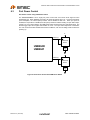
6.3
Port Power Control
Port Power Control Using USB Power Switch
The USB2640/USB2641 has a single port power control and over-current sense signal for each
downstream port. When disabling port power, the driver will actively drive a '0'. To avoid unnecessary
power dissipation, the internal pull-up resistor will be disabled at that time. When port power is
enabled, the output driver is disabled, and the pull-up resistor is enabled creating an open drain output.
If there is an over-current situation, the USB Power Switch will assert the open drain OCS signal. The
Schmitt trigger input will recognize this situation as a low. The open drain output does not interfere.
The over-current sense filter handles the transient conditions, such as low voltage, while the device is
powering up.
5V
PRTCTL3
OCS
USB Power
Switch
EN
USB2640/
USB2641
USB
Device
5V
PRTCTL2
OCS
USB Power
Switch
EN
USB
Device
Figure 6.1 Port Power Control with USB Power Switch
Revision 2.0 (10-03-08)
24
DATASHEET
SMSC USB2640/USB2641
Ultra Fast USB 2.0 Multi-Format Flash Media Controller/USB Hub Combo
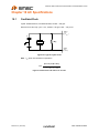
Port Power Control Using a Poly Fuse
When using the USB2640/USB2641 with a poly fuse, an external diode must be used (See Figure
6.2). When disabling port power, the driver will drive a '0'. This procedure will have no effect since the
external diode will isolate the pin from the load. When port power is enabled, the output driver is
disabled, and the pull-up resistor is enabled which creates an open drain output. This means that the
pull-up resistor is providing 3.3V to the anode of the diode. If there is an over-current situation, the
poly fuse will open. This will cause the cathode of the diode to go to 0V. The anode of the diode will
be at 0.7V, and the Schmitt trigger input will register this as a low resulting in an over-current detection.
The open drain output does not interfere.
5V
PRTCTL3
USB
Device
USB2640/
USB2641
5V
PRTCTL2
USB
Device
Figure 6.2 Port Power Control with Single Poly Fuse and Multiple Loads
When using a single poly fuse to power all devices, note that for the ganged situation, all power control
pins must be tied together.
5V
PRTCTL3
USB2640/
USB2641
PRTCTL2
Poly Fuse
USB
Device
USB
Device
Figure 6.3 Port Power with Ganged Control with Poly Fuse
SMSC USB2640/USB2641
25
DATASHEET
Revision 2.0 (10-03-08)
Ultra Fast USB 2.0 Multi-Format Flash Media Controller/USB Hub Combo
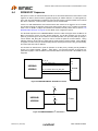
6.4
ROM BOOT Sequence
After power-on reset, the internal firmware checks for an external SPI flash device that contains a valid
signature of "2DFU" (device firmware upgrade) beginning at address 0xFFFA. If a valid signature is
found, then the external ROM is enabled and code execution begins at address 0x0000 in the external
SPI device. Otherwise, code execution continues from the internal ROM.
If there is no SPI ROM detected, the internal firmware then checks for the presence of an I2C ROM.
The firmware looks for the signature ‘ATA2’ at the offset of 0xFC-0xFF in the I2C ROM. The firmware
reads in the I2C ROM to configure the hardware and software internally. Please refer to section 7.3.2
EEPROM Data Descriptor on page 28 for the details of the configuration options.
The SPI ROM required for the USB2640/USB2641 must be 1 Mbit and support either 30 MHz or 60
MHz. The frequency used is set using the SPI_SPD_SEL. For 30 MHz operation, this pin must be
pulled to ground through a 100 kΩ resistor. For 60 MHz operation, this pin must pulled up through a
100 kΩ resistor. SPI_SPD_SEL: This pin is used to choose the speed of the SPI interface. During
nRESET assertion, this pin will be tri-stated with the weak pull-down resistor enabled. When nRESET
is negated, the value on the pin will be internally latched, and the pin will revert to SPI_DO functionality,
the internal pull-down will be disabled.
The firmware can determine the speed of operation on the SPI port by checking the SPI_SPEED in
the SPI_CTL register (0x2400 - RESET = 0x02). Both 1- and 2-bit SPI operation is supported. For
optimum throughput, a 2-bit SPI ROM is recommended. Both mode 0 and mode 3 SPI ROMS are also
supported.
USB2640/
USB2641
SPI_CE_N
CE#
SPI_CLK / GPIO4 / SCL
CLK
SPI ROM
SPI_DO / GPIO5 / SDA / SPI_SPD_SEL
DO
DI
SPI_DI
Figure 6.4 USB2640/USB2641 SPI ROM Connection
3.3V
10K
SCL
3.3V
USB2640/
USB2641
10K
I2C ROM
SDA
Figure 6.5 USB2640/USB2641 I2C Connection
Revision 2.0 (10-03-08)
26
DATASHEET
SMSC USB2640/USB2641
Ultra Fast USB 2.0 Multi-Format Flash Media Controller/USB Hub Combo
Chapter 7 Configuration Options
7.1
Hub
SMSC’s USB 2.0 hub is fully compliant to the Universal Serial Bus Specification available from the
USB Implementer’s Forum found at http://www.usb.org (Revision 2.0 April 27, 2000 and the 12/7/2000
and 5/28/2002 Errata) . Please reference Chapter 11 (Hub Specification) for general details regarding
hub operation and functionality.
The hub provides 1 transaction translator (TT) that is shared by both downstream ports (defined as
single-TT configuration). The TT contains 4 non-periodic buffers.
7.1.1
Hub Configuration Options
The SMSC hub supports a large number of features (some are mutually exclusive), and must be
configured in order to correctly function when attached to a USB host controller. There are two principal
ways to configure the hub; The internal default settings or by settings stored in an external EEPROM
or SPI Flash device.
7.1.1.1
Power Switching Polarity
The hub only supports “active high” port power controllers.
7.1.2
VBus Detect
According to Section 7.2.1 of the USB 2.0 Specification, a downstream port can never provide power
to its D+ or D- pull-up resistors unless the upstream port’s VBUS is in the asserted (powered) state.
The VBUS_DET pin on the hub monitors the state of the upstream VBUS signal and will not pull-up
the D+ resistor if VBUS is not active. If VBUS goes from an active to an inactive state (Not Powered),
the hub will remove power from the D+ pull-up resistor within 10 seconds.
7.2
Card Reader
The SMSC USB2640/USB2641 is fully compliant with the following flash media card reader
specifications:
Memory Stick Specification 1.43
Memory Stick Pro Format Specification 1.02
Memory Stick Pro-HG Duo Format Specification 1.01
-Memory Stick, MS Duo, HS-MS, MS Pro-HG, MS Pro
xD-Picture Card 1.2 compliant
Secure Digital 2.0 / MultiMediaCard Specification 4.3
-SD 2.0, HS-SD, HC-SD
-TransFlash™ and reduced form factor media
-1/4/8 bit MMC 4.2
7.3
System Configurations
7.3.1
EEPROM/SPI Interface
The USB2640/USB2641 can be configured via a 2-wire (I2C) EEPROM (256x8) or an external SPI
flash device containing the firmware for the USB2640/USB2641. If an external configuration device
does not exist the internal default values will be used. If one of the external devices is used for
SMSC USB2640/USB2641
27
DATASHEET
Revision 2.0 (10-03-08)
Ultra Fast USB 2.0 Multi-Format Flash Media Controller/USB Hub Combo
configuration, the OEM can update the values through the USB interface. The hub will then “attach”
to the upstream USB host.
When using an external SPI Flash, the register addresses in the following three tables (Table 7.1,
Table 7.2, ) refer to offsets from the starting location ‘FE80h’.
7.3.2
EEPROM Data Descriptor
Table 7.1 Internal Flash Media Controller Configurations
REG ADDR
REGISTER NAME
REGISTER DESCRIPTION
DEFAULT VALUE
00h-19h
USB_SER_NUM
USB Serial Number
"0000002640001" (Unicode)
1Ah-1Bh
USB_VID
USB Vendor ID
0424
1Ch-1Dh
USB_PID
USB Product ID
4050
1Eh-21h
USB_LANG_ID
USB Language Identifier
0409
22h-5Dh
USB_MFR_STR
USB Manufacturer String
“Generic” (Unicode)
5Eh-99h
USB_PRD_STR
USB Product String
"Ultra Fast Media Reader"
(Unicode)
9Ah
USB_BM_ATT
USB BmAttribute
80h
9Bh
USB_MAX_PWR
USB Max Power
30h (96 mA)
9Ch
ATT_LB
Attribute Lo byte
40h (Reverse SD_WP only)
9Dh
ATT_HLB
Attribute Hi Lo byte
00h
9Eh
ATT_LHB
Attribute Lo Hi byte
00h
9Fh
ATT_HB
Attribute Hi byte
00h
A0h
Reserved
-
A1h
Reserved
-
00h
A2h
Reserved
-
80h
A3h
Reserved
-
00h
A4h
LUN_PWR_LB
LUN Power Lo byte
00h
A5h
LUN_PWR_HB
LUN Power Hi byte
08h
A6h
Reserved
-
00h
A7h
Reserved
-
00h
A8h
LED_BLK_INT
Led Blink Interval
02h
A9h
LED_BLK_DUR
Led Blink After Access
28h
AAh - B0h
LUN0_ID_STR
Lun 0 Identifer String
“COMBO”
B1h - B7h
LUN1_ID_STR
Lun 1 Identifer String
“MS”
B8h - BEh
LUN2_ID_STR
Lun 2 Identifer String
“SM”
(See Note 7.1)
BFh - C5h
LUN3_ID_STR
Lun 3 Identifer String
“SD/MMC”
C6h - CDh
INQ_VEN_STR
Inquiry Vendor String
“Generic”
Revision 2.0 (10-03-08)
28
DATASHEET
SMSC USB2640/USB2641
Ultra Fast USB 2.0 Multi-Format Flash Media Controller/USB Hub Combo
Table 7.1 Internal Flash Media Controller Configurations (continued)
REG ADDR
REGISTER NAME
REGISTER DESCRIPTION
DEFAULT VALUE
CEh - D2h
INQ_PRD_STR
Inquiry Product String
2640
D3h
DYN_NUM_LUN
Dynamic Number of Luns
FFh
D4h - D7h
LUN_DEV_MAP
Lun to Device Mapping
FFh, FFh, FFh, FFh
D8h - DAh
Reserved
-
00h, 04h, 09h
DBh - DDh
Reserved
-
5Ch, 59h, 9Ah
Note 7.1
This value will be overridden with xD once an xD-Picture Card has been identified.
Table 7.2 Hub Controller Configurations
REG ADDR
REGISTER NAME
REGISTER DESCRIPTION
DEFAULT VALUE
DEh
VID_LSB
Vendor ID Least Significant Byte
24h
DFh
VID_MSB
Vendor ID Most Significant Byte
04h
E0h
PID_LSB
Product ID Least Significant Byte
40h
E1h
PID_MSB
Product ID Most Significant Byte
26h
E2h
DID_LSB
Device ID Least Significant Byte
00h
E3h
DID_MSB
Device ID Most Significant Byte
00h
E4h
CFG_DAT_BYT1
Configuration Data Byte 1
8Bh
E5h
CFG_DAT_BYT2
Configuration Data Byte 2
28h
E6h
CFG_DAT_BYT3
Configuration Data Byte 3
00h
E7h
NR_DEVICE
Non-Removable Devices
02h
E8h
PORT_DIS_SP
Port Disable (Self)
00h
E9h
PORT_DIS_BP
Port Disable (Bus)
00h
EAh
MAX_PWR_SP
Max Power (Self)
01h
EBh
MAX_PWR_BP
Max Power (Bus)
32h
ECh
HC_MAX_C_SP
Hub Controller Max Current (Self)
01h
EDh
HC_MAX_C_BP
Hub Controller Max Current (Bus)
32h
EEh
PWR_ON_TIME
Power-on Time
32h
EFh
BOOST_UP
Boost_Up
00h
F0h
BOOST_3:0
Boost_3:0
00h
F1h
PRT_SWP
Port Swap
00h
F2h
PRTR12
Port Remap 12
00h
F3h
PRTR3
Port Remap 3
00h
SMSC USB2640/USB2641
29
DATASHEET
Revision 2.0 (10-03-08)
Ultra Fast USB 2.0 Multi-Format Flash Media Controller/USB Hub Combo
Table 7.3 Other Internal Configurations
REG ADDR
REGISTER NAME
REGISTER DESCRIPTION
DEFAULT VALUE
F4h
MS_SD_CLK_LIM
MS/SD Clock Limit for
Flash Media Controller
00h
F5h
N/A
Reserved
66h
F6h
N/A
Reserved
00h
F7-FBh
N/A
Reserved
00h
FCh-FFh
NVSTORE_SIG
Non-volatile storage signature
(“ATA2”)
“ATA2”
7.3.2.1
0h-19h: USB Serial Number Option
BYTE
NUMBER
BYTE NAME
25:0
USB_SER_NUM
DESCRIPTION
Default Value is: UNICODE "0000002640001".
Maximum string length is 12 hex digits. Must be unique to each device.
7.3.2.2
1Ah-1Bh: USB Vendor ID Option
BYTE
NUMBER
BYTE NAME
1:0
USB_VID
7.3.2.3
DESCRIPTION
This ID is unique for every vendor. The vendor ID is assigned by the USB
Implementers Forum.
1Ch-1Dh: USB Product ID Option
BYTE
NUMBER
BYTE NAME
DESCRIPTION
1:0
USB_PID
This ID is unique for every product. The product ID is assigned by the vendor.
7.3.2.4
1Eh-21h: USB Language Identifier Option
BYTE
NUMBER
BYTE NAME
3:0
USB_LANG_ID
DESCRIPTION
USB LANGUAGE ID
English Language Code = ‘0409’. Please refer to the USB 2.0 specification
for Other Language Codes.
Revision 2.0 (10-03-08)
30
DATASHEET
SMSC USB2640/USB2641
Ultra Fast USB 2.0 Multi-Format Flash Media Controller/USB Hub Combo
7.3.2.5
22h-5Dh: USB Manufacturer String Length
BYTE
NUMBER
BYTE NAME
59:0
USB_MFR_STR
DESCRIPTION
Manufacturer String Length
Maximum string length is 28 characters.
(See Note 7.2 below)
7.3.2.6
5Eh-99h: USB Product String Length
BYTE
NUMBER
BYTE NAME
59:0
USB_PRD_STR
DESCRIPTION
Product String Length
This string will be used during the USB enumeration process in Windows.
Maximum string length is 28 characters.
(See Note 7.2 below)
Note 7.2
7.3.2.7
While the full strings are reported during USB enumeration, Windows XP/Vista reads
concatenated version of the strings from the standard SCSI inquiry response when storing
the values for display in the Windows registry and device manager.
9Ah: USB BmAttribute (1 byte)
BYTE
NUMBER
BYTE NAME
7:0
USB_BM_ATT
DESCRIPTION
Self- or Bus-Power: Selects between Self- and Bus-Powered operation.
The hub is either Self-Powered (draws less than 2 mA of upstream bus
power) or Bus-Powered (limited to a 100 mA maximum of upstream power
prior to being configured by the host controller).
When configured as a Bus-Powered device, the SMSC hub consumes less
than 100 mA of current prior to being configured. After configuration, the
Bus-Powered SMSC hub (along with all associated hub circuitry, any
embedded devices if part of a compound device, and 100 mA per externally
available downstream port) must consume no more than 500 mA of
upstream VBUS current. The current consumption is system dependent, and
the OEM must ensure that the USB 2.0 specifications are not violated.
When configured as a Self-Powered device, <1 mA of upstream VBUS
current is consumed and all ports are available, with each port being capable
of sourcing 500 mA of current.
80 = Bus-Powered operation
c0 = Self-Powered operation
A0 = Bus-Powered operation with remote wake-up
E0 = Self-Powered operation with remote wake-up
SMSC USB2640/USB2641
31
DATASHEET
Revision 2.0 (10-03-08)
Ultra Fast USB 2.0 Multi-Format Flash Media Controller/USB Hub Combo
7.3.2.8
9Bh: USB MaxPower (1 byte)
BYTE
NUMBER
BYTE NAME
DESCRIPTION
7:0
USB_MAX_PWR
USB Max Power Per USB specification. Do NOT set this value greater than
100 mA.
7.3.2.9
9Ch-9Fh: Attribute Byte Descriptions
BYTE
BYTE
NAME
BIT
NUMBER
1
ATT_LB
3:0
4
DESCRIPTION
Always reads ‘0’.
Inquire Manufacturer and Product ID Strings
1 - Use the Inquiry Manufacturer and Product ID Strings.
0 (default) - Use the USB Descriptor Manufacturer and Product ID Strings.
2
ATT_HLB
5
Activity GPIO High when Suspended
1 - The activity LED GPIO is set to High when suspended.
0 (default) - The activity LED GPIO is set to Low when suspended.
6
Reverse SD Card Write Protect Sense
1 (default) - SD cards will be write protected when SW_nWP is high, and
writable when SW_nWP is low.
0 - SD cards will be write protected when SW_nWP is low, and writable
when SW_nWP is high.
7
Always reads ‘0’.
3:0
Always reads ‘0’.
4
Activity LED True polarity
1 - Activity LED to Low True.
0 (default) - Activity LED polarity to High True.
5
Common Media Insert / Media Activity LED
1 - The activity LED will function as a common media inserted/media
access LED.
0 (default) - The activity LED will remain in its idle state until media is
accessed.
7:6
3
4
ATT_LHB
ATT_HB
Revision 2.0 (10-03-08)
Always reads ‘0’.
0
Attach on Card Insert / Detach on Card Removal
1 - Attach on Insert is enabled
0 (default) - Attach on Insert is disabled
1
Always reads ‘0’.
2
Use Lun Power Configuration.
1 - Custom LUN Power Configuration stored in the NVSTORE is used.
0 (default) - Default LUN Power Configuration is used.
7:3
Always reads ‘0’.
6:0
Always reads ‘0’.
7
xD Player Mode
32
DATASHEET
SMSC USB2640/USB2641
Ultra Fast USB 2.0 Multi-Format Flash Media Controller/USB Hub Combo
7.3.2.10
A4h-A5h: LUN Power Configuration
The USB2640/USB2641 has one internal FET which can be utilized for card power. The settings are
stored in NVSTORE and provide the following features:
1.A card can be powered by an external FET or internal FET.
2.The power limit can be set to 100 mA (Default) or 200 mA for the internal FET.
Each media uses two bytes to store its LUN power configuration. Bit 3 selects between internal or
external. For internal FETs Bits 0 through 2 are used for the power limit. Only 2 of the possible 8 values
are currently specified.
Table 7.4 FET Configuration
FET
TYPE
BITS
0
FET Low
Byte
3:0
Low Nibble
Unused.
7:4
High Nibble
Unused.
FET High
Byte
3:0
Low Nibble
0000b
0001b
1000b
1010b
7:4
High Nibble
Unused.
1
2
3
7.3.2.11
BIT TYPE
DESCRIPTION
Disabled.
External FET Enabled.
Internal FET with 100 mA power limit.
Internal FET with 200 mA power limit.
A8h: LED Blink Interval (1 byte)
BIT
NUMBER
BIT NAME
DESCRIPTION
7:0
LED_BLK_INT
The blink rate is programmable in 10 ms intervals. Hi bit indicates idle state:
0-Off, 1-On. The remaining bits are used to determine the blink interval up
to a max of 128 x 10 ms.
7.3.2.12
A9h: Blink Duration (1 byte)
BIT
NUMBER
BIT NAME
7:0
LED_BLK_DUR
7.3.3
DESCRIPTION
LED blink After Access. This byte is used to designate the number of
seconds that the GPIO 0 LED will continue to blink after a drive access.
Setting this byte to "05" will cause the GPIO 0 LED to blink for 5 seconds
after a drive access.
LUN ID Strings
There are four LUN ID strings corresponding to LUN# 0, 1, 2, and 3: Number of Icons to Display, SM
LUN #, MS LUN #, SD/MMC LUN #. The SM value will be overridden with xD once an xD-Picture Card
has been identified.
SMSC USB2640/USB2641
33
DATASHEET
Revision 2.0 (10-03-08)
Ultra Fast USB 2.0 Multi-Format Flash Media Controller/USB Hub Combo
7.3.3.1
AAh-B0h: Lun 0 Identifier String
BYTE
NUMBER
BYTE NAME
STRING
DESCRIPTION
6:0
LUN0_ID_STR
“COMBO”
These bytes are used to specify the LUN descriptor
returned by the device. These bytes are used in
combination with the LUN to device mapping bytes
in applications where the OEM wishes to reorder
and rename the LUNs or utilizes a combo socket
and wishes to rename the LUN.
7.3.3.2
B1h-B7h: Lun 1 Identifier String
BYTE
NUMBER
BYTE NAME
STRING
DESCRIPTION
6:0
LUN1_ID_STR
“MS”
These bytes are used to specify the LUN descriptor
returned by the device. These bytes are used in
combination with the LUN to device mapping bytes
in applications where the OEM wishes to reorder
and rename the LUNs or utilizes a combo socket
and wishes to rename the LUN.
7.3.3.3
B8h-BEh: Lun 2 Identifier String
BYTE
NUMBER
BYTE NAME
STRING
DESCRIPTION
6:0
LUN2_ID_STR
“SM”
These bytes are used to specify the LUN descriptor
returned by the device. These bytes are used in
combination with the LUN to device mapping bytes
in applications where the OEM wishes to reorder
and rename the LUNs or utilizes a combo socket
and wishes to rename the LUN.
7.3.3.4
BFh-C5h: Lun 3 Identifier String
BYTE
NUMBER
BYTE NAME
STRING
DESCRIPTION
6:0
LUN3_ID_STR
“SD/MMC”
These bytes are used to specify the LUN descriptor
returned by the device. These bytes are used in
combination with the LUN to device mapping bytes
in applications where the OEM wishes to reorder
and rename the LUNs or utilizes a combo socket
and wishes to rename the LUN.
7.3.3.5
C6h-CDh: Inquiry Vendor String
BYTE
NUMBER
BYTE NAME
STRING
DESCRIPTION
7:0
INQ_VEN_STR
“Generic”
If bit 4 of the 1st attribute byte is set, the device will
use these strings in response to a USB inquiry
command, instead of the USB Descriptor
Manufacturer and Product ID Strings.
Revision 2.0 (10-03-08)
34
DATASHEET
SMSC USB2640/USB2641
Ultra Fast USB 2.0 Multi-Format Flash Media Controller/USB Hub Combo
7.3.3.6
CEh-D2h: Inquiry Product String
BYTE
NUMBER
BYTE NAME
UINT
DESCRIPTION
4:0
INQ_PRD_STR
2640
If bit 4 of the 1st attribute byte is set, the device will
use these strings in response to a USB inquiry
command, instead of the USB Descriptor
Manufacturer and Product ID Strings.
7.3.3.7
D3h: Dynamic Number of Luns
BIT
NUMBER
BYTE NAME
UCHAR
DESCRIPTION
7:0
DYN_NUM_LUN
FFh
These bytes are used to specify the number of LUNs
the device exposes to the host. These bytes are also
used for icon sharing by assigning more than one
LUN to a single icon. This is used in applications
where the device utilizes a combo socket and the
OEM wishes to have only a single icon displayed for
one or more interfaces.
If this field is set to "FF", the program assumes that
you are using the default value of "04" and will
display icons for xD, MS, and SD/MMC. If this field
is any other value besides "FF", you must specify the
LUN# assignments in the boxes starting with LUN 00
and going to (# of Icons to Display -1).
Regardless of this setting, the USB2640/USB2641
sets this value to ‘1’.
7.3.3.8
D4h-D7h: Lun to Device Mapping
BYTE
NUMBER
BYTE NAME
UCHARS
DESCRIPTION
3:0
LUN_DEV_MAP
FFh, FFh, FFh, FFh
These bytes are used to specify the number of LUNs
the device exposes to the host. These bytes are also
used for icon sharing by assigning more than one
LUN to a single icon. This is used in applications
where the device utilizes a combo socket and the
OEM wishes to have only a single icon displayed for
one or more interfaces.
If this field is set to "FF", the program assumes that
you are using the default value of "04" and will
display icons for xD, MS, and SD/MMC. If this field
is any other value besides "FF", you must specify
the LUN# assignments in the boxes starting with
LUN 00 and going to (# of Icons to Display -1).
Regardless of this setting, the USB2640/USB2641
sets these values to ‘FFh, 00h, 00h, 00h’.
SMSC USB2640/USB2641
35
DATASHEET
Revision 2.0 (10-03-08)
Ultra Fast USB 2.0 Multi-Format Flash Media Controller/USB Hub Combo
7.3.3.9
D8h-DAh: Reserved
BIT
NUMBER
BYTE NAME
BITS
2:0
Reserved
00h, 04h, 09h
7.3.3.10
For internal use only.
DBh-DDh: Reserved
BIT
NUMBER
BYTE NAME
BITS
2:0
Reserved
5Ch, 59h, 9Ah
7.3.3.11
DESCRIPTION
DESCRIPTION
For internal use only.
DEh: Vendor ID (LSB)
BIT
NUMBER
BYTE NAME
DESCRIPTION
7:0
VID_LSB
Least Significant Byte of the Vendor ID. This is a 16-bit value that uniquely
identifies the Vendor of the user device (assigned by USB Implementers
Forum).
7.3.3.12
DFh: Vendor ID (MSB)
BIT
NUMBER
BYTE NAME
7:0
VID_MSB
7.3.3.13
DESCRIPTION
Most Significant Byte of the Vendor ID. This is a 16-bit value that uniquely
identifies the Vendor of the user device (assigned by USB Implementers
Forum).
E0h: Product ID (LSB)
BIT
NUMBER
BIT NAME
DESCRIPTION
7:0
PID_LSB
Least Significant Byte of the Product ID. This is a 16-bit value that the Vendor
can assign that uniquely identifies this particular product.
Revision 2.0 (10-03-08)
36
DATASHEET
SMSC USB2640/USB2641
Ultra Fast USB 2.0 Multi-Format Flash Media Controller/USB Hub Combo
7.3.3.14
E1h: Product ID (MSB)
BIT
NUMBER
BIT NAME
DESCRIPTION
7:0
PID_MSB
Most Significant Byte of the Product ID. This is a 16-bit value that the Vendor
can assign that uniquely identifies this particular product.
7.3.3.15
E2h: Device ID (LSB)
BIT
NUMBER
BIT NAME
7:0
DID_LSB
7.3.3.16
Least Significant Byte of the Device ID. This is a 16-bit device release
number in BCD (binary coded decimal) format.
E3h: Device ID (MSB)
BIT
NUMBER
BIT NAME
7:0
DID_MSB
7.3.3.17
DESCRIPTION
DESCRIPTION
Most Significant Byte of the Device ID. This is a 16-bit device release
number in BCD format.
E4h: Config Data Byte 1 (CFG_DAT_BYT1)
BIT
NUMBER
BIT NAME
7
SELF_BUS_PWR
DESCRIPTION
Self- or Bus-Power: Selects between Self- and Bus-Powered operation.
The hub is either Self-Powered (draws less than 2 mA of upstream bus
power) or Bus-Powered (limited to a 100 mA maximum of upstream power
prior to being configured by the host controller).
When configured as a Bus-Powered device, the SMSC hub consumes less
than 100 mA of current prior to being configured. After configuration, the
Bus-Powered SMSC hub (along with all associated hub circuitry, any
embedded devices if part of a compound device, and 100 mA per externally
available downstream port) must consume no more than 500 mA of
upstream VBUS current. The current consumption is system dependent, and
the OEM must ensure that the USB 2.0 specifications are not violated.
When configured as a Self-Powered device, <1 mA of upstream VBUS
current is consumed and all ports are available, with each port being capable
of sourcing 500 mA of current.
0 = Bus-Powered operation
1 = Self-Powered operation
6
Reserved
SMSC USB2640/USB2641
Always reads ‘0’.
37
DATASHEET
Revision 2.0 (10-03-08)
Ultra Fast USB 2.0 Multi-Format Flash Media Controller/USB Hub Combo
BIT
NUMBER
BIT NAME
DESCRIPTION
5
HS_DISABLE
Hi-Speed Disable: Disables the capability to attach as either a Hi-/Full-Speed
device, and forces attachment as Full-Speed only (i.e. no Hi-Speed support).
0 = Hi-/Full-Speed
1 = Full-Speed-Only (Hi-Speed disabled!)
4
Reserved
3
EOP_DISABLE
Always reads ‘0’.
EOP Disable: Disables EOP generation of EOF1 when in Full-Speed mode.
During FS operation only, this permits the hub to send EOP if no
downstream traffic is detected at EOF1. See Section 11.3.1 of the USB 2.0
Specification for additional details. Note: generation of an EOP at the EOF1
point may prevent a Host Controller (operating in FS mode) from placing the
USB bus in suspend.
0 = An EOP is generated at the EOF1 point if no traffic is detected.
1 = EOP generation at EOF1 is disabled (Note: This is normal USB
operation).
Note:
2:1
CURRENT_SNS
This is a rarely used feature in the PC environment, existing drivers
may not have been thoroughly debugged with this feature enabled.
It is included because it is a permitted feature in Chapter 11 of the
USB specification.
Over-Current Sense: Selects current sensing on a port-by-port basis, all
ports ganged, or none (only for bus-powered hubs). The ability to support
current sensing on a port or ganged basis is dependent upon the hardware
implementation.
00 = Ganged sensing (all ports together)
01 = Individual port-by-port
1x = Over-current sensing not supported (must only be used with BusPowered configurations!)
0
PORT_PWR
Port Power Switching: Enables power switching on all ports simultaneously
(ganged), or port power is individually switched on and off on a port- by-port
basis (individual). The ability to support power enabling on a port or ganged
basis is dependent upon the hardware implementation.
0 = Ganged switching (all ports together)
1 = Individual port-by-port switching
7.3.3.18
E5h: Config Data Byte 2 (CFG_DAT_BYT2)
BIT
NUMBER
BIT NAME
7:6
Reserved
5:4
OC_TIMER
DESCRIPTION
Always reads ‘0’.
OverCurrent Timer: Over-current Timer delay.
00 = 50 ns
01 = 100 ns
10 = 200 ns
11 = 400 ns
Revision 2.0 (10-03-08)
38
DATASHEET
SMSC USB2640/USB2641
Ultra Fast USB 2.0 Multi-Format Flash Media Controller/USB Hub Combo
BIT
NUMBER
BIT NAME
DESCRIPTION
3
COMPOUND
Compound Device: Allows OEM to indicate that the hub is part of a
compound (see the USB Specification for definition) device. The
applicable port(s) must also be defined as having a "Non-Removable
Device".
Note:
When configured via strapping options, declaring a port as nonremovable automatically causes the hub controller to report that it
is part of a compound device.
0 = No
1 = Yes, the hub is part of a compound device
2:0
7.3.3.19
Always reads ‘0’.
Always reads ‘0’.
E6h: Config Data Byte 3 (CFG_DAT_BYT3)
BIT
NUMBER
BIT NAME
7:4
Reserved
3
PRTMAP_EN
DESCRIPTION
Always reads ‘0’.
Port Re-mapping enable: Selects the method used by the hub to assign port
numbers and disable ports.
‘0’ = Standard Mode. Strap options or the following registers are used to
define which ports are enabled, and the ports are mapped as Port ‘n’ on the
jub is reported as Port ‘n’ to the host, unless one of the ports is disabled,
then the higher numbered ports are remapped in order to report contiguous
port numbers to the host.
Register 300Ah: Port Disable For Self-Powered Operation (Reset = 0x00).
Register 300Bh: Port Disable For Bus-Powered Operation (Reset = 0x00).
‘1’ = Port Re-map mode. The mode enables remapping via the registers
defined below.
Register 30FBh: Port Remap 12 (Reset = 0x00)
Register 30FCh: Port Remap 3 (Reset = 0x00)
2:0
Reserved
SMSC USB2640/USB2641
Always reads ‘0’.
39
DATASHEET
Revision 2.0 (10-03-08)
Ultra Fast USB 2.0 Multi-Format Flash Media Controller/USB Hub Combo
7.3.3.20
E7h: Non-Removable Device
BIT
NUMBER
BYTE NAME
7:0
NR_DEVICE
DESCRIPTION
Non-removable Device: Indicates which port(s) include non-removable
devices. ‘0’ = port is removable, ‘1’ = port is non-removable.
Informs the host if one of the active ports has a permanent device that is
undetachable from the hub. (Note: The device must provide its own
descriptor data.)
When using the internal default option, the NON_REM[1:0] pins will
designate the appropriate ports as being non-removable.
Bit
Bit
Bit
Bit
Bit
Bit
Bit
Bit
7=
6=
5=
4=
3=
2=
1=
0=
Note:
7.3.3.21
Reserved
Reserved
Reserved
Reserved
1; port 3 non-removable
1; Port 2 non-removable
1; Port 1 non removable
Reserved, always = ‘0’
Bit 1 must be set to a ‘1’ by the firmware for proper identification of
the card reader as a non-removable device.
E8h: Port Disable For Self-Powered Operation
BIT
NUMBER
BYTE NAME
DESCRIPTION
7:0
PORT_DIS_SP
Port Disable Self-Powered: Disables 1 or more ports. ‘0’ = port is available,
‘1’ = port is disabled.
During Self-Powered operation this register selects the ports which will be
permanently disabled. The ports are unavailable to be enabled or
enumerated by a Host Controller. The ports can be disabled in any order
since the internal logic will automatically report the correct number of
enabled ports to the USB host and will reorder the active ports in order to
ensure proper function.
Bit
Bit
Bit
Bit
Bit
Bit
Bit
Bit
Revision 2.0 (10-03-08)
7=
6=
5=
4=
3=
2=
1=
0=
Reserved
Reserved
Reserved
Reserved
1; Port 3 is disabled
1; Port 2 is disabled
1; Port 1 is disabled
Reserved, always = ‘0’
40
DATASHEET
SMSC USB2640/USB2641
Ultra Fast USB 2.0 Multi-Format Flash Media Controller/USB Hub Combo
7.3.3.22
E9h: Port Disable For Bus-Powered Operation
BIT
NUMBER
BYTE NAME
DESCRIPTION
7:0
PORT_DIS_BP
Port Disable Bus-Powered: Disables 1 or more ports. ‘0’ = port is available,
‘1’ = port is disabled.
During Self-Powered operation, this register selects the ports which will be
permanently disabled. The ports are unavailable to be enabled or
enumerated by a Host Controller. The ports can be disabled in any order,
the internal logic will automatically report the correct number of enabled ports
to the USB host and will reorder the active ports in order to ensure proper
function.
When using the internal default option, the PRT_DIS[1:0] pins will disable the
appropriate ports.
Bit
Bit
Bit
Bit
Bit
Bit
Bit
Bit
7.3.3.23
7= Reserved
6= Reserved
5= Reserved
4= Reserved
3= 1; Port 3 is
2= 1; Port 2 is
1= 1; Port 1 is
0 is Reserved,
disabled
disabled
disabled
always = ‘0’
EAh: Max Power For Self-Powered Operation
BIT
NUMBER
BYTE NAME
DESCRIPTION
7:0
MAX_PWR_SP
Max Power Self_Powered: Value in 2 mA increments that the hub consumes
from an upstream port (VBUS) when operating as a self-powered hub. This
value includes the hub silicon along with the combined power consumption
(from VBUS) of all associated circuitry on the board. This value also includes
the power consumption of a permanently attached peripheral if the hub is
configured as a compound device, and the embedded peripheral reports 0
mA in its descriptors.
Note:
7.3.3.24
The USB 2.0 Specification does not permit this value to exceed 100
mA.
EBh: Max Power For Bus-Powered Operation
BIT
NUMBER
BYTE NAME
DESCRIPTION
7:0
MAX_PWR_BP
Max Power Bus_Powered: Value in 2 mA increments that the hub consumes
from an upstream port (VBUS) when operating as a bus-powered hub. This
value includes the hub silicon along with the combined power consumption
(from VBUS) of all associated circuitry on the board. This value also includes
the power consumption of a permanently attached peripheral if the hub is
configured as a compound device, and the embedded peripheral reports 0
mA in its descriptors.
SMSC USB2640/USB2641
41
DATASHEET
Revision 2.0 (10-03-08)
Ultra Fast USB 2.0 Multi-Format Flash Media Controller/USB Hub Combo
7.3.3.25
ECh: Hub Controller Max Current For Self-Powered Operation
BIT
NUMBER
BYTE NAME
DESCRIPTION
7:0
HC_MAX_C_SP
Hub Controller Max Current Self-Powered: Value in 2 mA increments that the
hub consumes from an upstream port (VBUS) when operating as a selfpowered hub. This value includes the hub silicon along with the combined
power consumption (from VBUS) of all associated circuitry on the board.
This value does NOT include the power consumption of a permanently
attached peripheral if the hub is configured as a compound device.
Note:
The USB 2.0 Specification does not permit this value to exceed 100
mA.
A value of 50 (decimal) indicates 100 mA, which is the default value.
7.3.3.26
EDh: Hub Controller Max Current For Bus-Powered Operation
BIT
NUMBER
BYTE NAME
DESCRIPTION
7:0
HC_MAX_C_BP
Hub Controller Max Current Bus-Powered: Value in 2 mA increments that the
hub consumes from an upstream port (VBUS) when operating as a buspowered hub. This value will include the hub silicon along with the combined
power consumption (from VBUS) of all associated circuitry on the board.
This value will NOT include the power consumption of a permanently
attached peripheral if the hub is configured as a compound device.
A value of 50 (decimal) would indicate 100 mA, which is the default value.
7.3.3.27
EEh: Power-On Time
BIT
NUMBER
BYTE NAME
DESCRIPTION
7:0
POWER_ON_TIME
Power-On Time: The length of time that it takes (in 2 ms intervals) from the
time the host initiated power-on sequence begins on a port until power is
adequate on that port. System software uses this value to determine how
long to wait before accessing a powered-on port.
Revision 2.0 (10-03-08)
42
DATASHEET
SMSC USB2640/USB2641
Ultra Fast USB 2.0 Multi-Format Flash Media Controller/USB Hub Combo
7.3.3.28
EFh: Boost_Up
BIT
NUMBER
BIT NAME
7:2
Reserved
1:0
BOOST_IOUT
DESCRIPTION
Reserved
USB electrical signaling drive strength Boost Bit for the Upstream Port ‘A’.
‘00’ = Normal electrical drive strength = No boost
‘01’ = Elevated electrical drive strength = Low (approximately 4% boost)
‘10’ = Elevated electrical drive strength = Medium (approximately 8% boost)
‘11’ = Elevated electrical drive strength = High (approximately 12% boost)
Note:
7.3.3.29
“Boost” could result in non-USB Compliant parameters (one
example would be Test J/K levels), OEM should use a ‘00’ value
unless specific implementation issues require additional signal
boosting to correct for degraded USB signalling levels.
F0h: Boost_3:0
BIT
NUMBER
BIT NAME
7:6
Reserved
5:4
BOOST_IOUT_3
DESCRIPTION
Always reads ‘0’.
Upstream USB electrical signaling drive strength Boost Bit for Downstream
Port ‘3’.
‘00’ = Normal electrical drive strength = No boost
‘01’ = Elevated electrical drive strength = Low (approximately 4% boost)
‘10’ = Elevated electrical drive strength = Medium (approximately 8% boost)
‘11’ = Elevated electrical drive strength = High (approximately 12% boost)
3:2
BOOST_IOUT_2
Upstream USB electrical signaling drive strength Boost Bit for Downstream
Port ‘2’.
‘00’ = Normal electrical drive strength = No boost
‘01’ = Elevated electrical drive strength = Low (approximately 4% boost)
‘10’ = Elevated electrical drive strength = Medium (approximately 8% boost)
‘11’ = Elevated electrical drive strength = High (approximately 12% boost)
Note:
1:0
Reserved
SMSC USB2640/USB2641
“Boost” could result in non-USB Compliant parameters (one
example would be Test J/K levels), OEM should use a ‘00’ value
unless specific implementation issues require additional signal
boosting to correct for degraded USB signalling levels.
Always reads ‘0’.
43
DATASHEET
Revision 2.0 (10-03-08)
Ultra Fast USB 2.0 Multi-Format Flash Media Controller/USB Hub Combo
7.3.3.30
F1h: Port Swap
BIT
NUMBER
BYTE NAME
DESCRIPTION
7:0
PRT_SWP
Port Swap: Swaps the Upstream and Downstream USB DP and DM Pins for
ease of board routing to devices and connectors.
‘0’ = USB D+ functionality is associated with the DP pin and D- functionality
is associated with the DM pin.
‘1’ = USB D+ functionality is associated with the DM pin and D- functionality
is associated with the DP pin.
Bit
Bit
Bit
Bit
Bit
Bit
Bit
Bit
Revision 2.0 (10-03-08)
7=
6=
5=
4=
3=
2=
1=
0=
Reserved
Reserved
Reserved
Reserved
‘1’; Port 3 DP/DM is swapped
‘1’; Port 2 DP/DM is swapped
Reserved
‘1’:Upstream Port DP/DM is swapped
44
DATASHEET
SMSC USB2640/USB2641
Ultra Fast USB 2.0 Multi-Format Flash Media Controller/USB Hub Combo
7.3.3.31
F2h: Port Remap 12
BIT
NUMBER
BYTE NAME
7:0
PRTR12
DESCRIPTION
Port remap register for ports 1 & 2.
When a hub is enumerated by a USB Host Controller, the hub is only
permitted to report how many ports it has; the hub is not permitted to select
a numerical range or assignment. The Host Controller will number the
downstream ports of the hub starting with the number '1', up to the number
of ports that the hub reported having.
The host's port number is referred to as "Logical Port Number" and the
physical port on the hub is the “Physical Port Number". When remapping
mode is enabled (see PRTMAP_EN in Register 08h: Configuration Data
Byte 3) the hub's downstream port numbers can be remapped to different
logical port numbers (assigned by the host).
Note:
OEM must ensure that Contiguous Logical Port Numbers are used,
starting from number ‘1’ up to the maximum number of enabled
ports; this ensures that the hub's ports are numbered in accordance
with the way a host will communicate with the ports.
Table 7.5 Port Remap Register for Ports 1 & 2
Bit [7:4]
Bit [3:0]
SMSC USB2640/USB2641
45
‘0000’
Physical Port 2 is Disabled
‘0001’
Physical Port 2 is mapped to Logical Port 1
‘0010’
Physical Port 2 is mapped to Logical Port 2
‘0011’
Physical Port 2 is mapped to Logical Port 3
‘0100’
to
‘1111’
Illegal; Do Not Use
‘0000’
Physical Port 1 is Disabled
‘0001’
Physical Port 1 is mapped to Logical Port 1
‘0010’
Physical Port 1 is mapped to Logical Port 2
‘0011’
Physical Port 1 is mapped to Logical Port 3
‘0100’
to
‘1111’
Illegal; Do Not Use
DATASHEET
Revision 2.0 (10-03-08)
Ultra Fast USB 2.0 Multi-Format Flash Media Controller/USB Hub Combo
7.3.3.32
F3h: Port Remap 3
BIT
NUMBER
BYTE NAME
7:0
PRTR3
DESCRIPTION
Port remap register for port 3.
When a hub is enumerated by a USB Host Controller, the hub is only
permitted to report how many ports it has; the hub is not permitted to select
a numerical range or assignment. The Host Controller will number the
downstream ports of the hub starting with the number '1', up to the number
of ports that the hub reported having.
The host's port number is referred to as "Logical Port Number" and the
physical port on the hub is the “Physical Port Number". When remapping
mode is enabled (see PRTMAP_EN in Register 08h: Configuration Data
Byte 3) the hub's downstream port numbers can be remapped to different
logical port numbers (assigned by the host).
Note:
OEM must ensure that Contiguous Logical Port Numbers are used,
starting from number ‘1’ up to the maximum number of enabled
ports; this ensures that the hub's ports are numbered in accordance
with the way a host will communicate with the ports.
Table 7.6 Port Remap Register for Port 3
Bit [7:4]
Bit [3:0]
Revision 2.0 (10-03-08)
46
‘0000’
Reserved
‘0001’
Reserved
‘0010’
Reserved
‘0011’
Reserved
‘0100’
to
‘1111’
Illegal; Do Not Use
‘0000’
Physical Port 3 is Disabled
‘0001’
Physical Port 3 is mapped to Logical Port 1
‘0010’
Physical Port 3 is mapped to Logical Port 2
‘0011’
Physical Port 3 is mapped to Logical Port 3
‘0100’
to
‘1111’
Illegal; Do Not Use
DATASHEET
SMSC USB2640/USB2641
Ultra Fast USB 2.0 Multi-Format Flash Media Controller/USB Hub Combo
7.3.3.33
F4h: MS/SD Clock Limit
BYTE NAME
MS_SD_CLK_LIM
7.3.3.34
TYPE
BITS
DESCRIPTION
Upper
Nibble Bits
7:4
0:
1:
2:
3:
MS
MS
MS
MS
Lower
Nibble Bits
3:0
0:
1:
2:
3:
SD/MMC
SD/MMC
SD/MMC
SD/MMC
BYTE NAME
DEFAULT VALUE
7:0
Reserved
66h
MHz -- Default, no limit
MHz
MHz
MHz
-
48
24
20
15
MHz
MHz
MHz
MHz
DESCRIPTION
Reserved.
F6h: Reserved
BIT
NUMBER
BYTE NAME
DEFAULT VALUE
7:0
Reserved
00h
7.3.3.36
60
40
20
15
F5h: Reserved
BIT
NUMBER
7.3.3.35
-
DESCRIPTION
Reserved for media usage.
FCh-FFh: Non-volatile Storage Signature
BYTE
NUMBER
BYTE NAME
STRING
DESCRIPTION
7:0
NVSTORE_SIG
“ATA2”
This signature is used to verify the validity of the
data in the configuration area. The signature must be
set to ‘ATA2’ for USB2640/USB2641.
7.3.4
I2C EEPROM
The I2C EEPROM interface implements a subset of the I2C Master Specification (Please refer to the
Philips Semiconductor Standard I2C-Bus Specification for details on I2C bus protocols). The device’s
I2C EEPROM interface is designed to attach to a single “dedicated” I2C EEPROM, and it conforms to
the Standard-mode I2C Specification (100 kbit/s transfer rate and 7-bit addressing) for protocol and
electrical compatibility.
Note: Extensions to the I2C Specification are not supported.
The device acts as the master and generates the serial clock SCL, controls the bus access
(determines which device acts as the transmitter and which device acts as the receiver), and generates
the START and STOP conditions.
SMSC USB2640/USB2641
47
DATASHEET
Revision 2.0 (10-03-08)
Ultra Fast USB 2.0 Multi-Format Flash Media Controller/USB Hub Combo
7.3.4.1
Implementation Characteristics
The device will only access an EEPROM using the Sequential Read Protocol.
7.3.4.2
Pull-Up Resistor
The circuit board designer is required to place external pull-up resistors (10 kΩ recommended) on the
SDA/SMBDATA & SCL/SMBCLK/CFG_SELO lines (per SMBus 1.0 Specification, and EEPROM
manufacturer guidelines) to Vcc in order to assure proper operation.
7.3.5
In-Circuit EEPROM Programming
The EEPROM can be programmed via ATE by pulling RESET_N low (which tri-states the device’s
EEPROM interface and allows an external source to program the EEPROM).
7.4
Default Configuration Option:
The SMSC device can be configured via its internal default configuration. Please see Section 7.3.2,
"EEPROM Data Descriptor" for specific details on how to enable default configuration.
Please refer to Table 7.1 for the internal default values that are loaded when this option is selected.
7.5
Reset
There are two different resets that the device experiences. One is a hardware reset (either from the
internal POR reset circuit or via the RESET_N pin) and the second is a USB Bus Reset.
7.5.1
Internal POR Hardware Reset
All reset timing parameters are guaranteed by design.
7.5.2
External Hardware RESET_N
A valid hardware reset is defined as assertion of RESET_N for a minimum of 1 μs after all power
supplies are within operating range. While reset is asserted, the device (and its associated external
circuitry) consumes less than 500 μA of current from the upstream USB power source.
Assertion of RESET_N (external pin) causes the following:
1. All downstream ports are disabled, and PRTCTL power to downstream devices is removed.
2. The PHYs are disabled, and the differential pairs will be in a high-impedance state.
3. All transactions immediately terminate; no states are saved.
4. All internal registers return to the default state (in most cases, 00h).
5. The external crystal oscillator is halted.
6. The PLL is halted.
Revision 2.0 (10-03-08)
48
DATASHEET
SMSC USB2640/USB2641
Ultra Fast USB 2.0 Multi-Format Flash Media Controller/USB Hub Combo
7.5.2.1
RESET_N for EEPROM Configuration
Hardware
reset
asserted
Device
Recovery/
Stabilization
8051 Sets
Configuration
Registers
Attach
USB
Upstream
USB Reset
recovery
Start
completion
request
response
Idle
t4
t1
t6
t5
t3
t2
t7
RESET_N
VSS
Figure 7.1 Reset_N Timing for EEPROM Mode
Table 7.7 Reset_N Timing for EEPROM Mode
NAME
DESCRIPTION
MIN
t1
RESET_N asserted.
t2
Device recovery/stabilization.
t3
8051 programs device configuration
t4
USB attach (See Note).
t5
Host acknowledges attach and signals USB reset.
t6
USB idle.
t7
Completion time for requests (with or without data
stage).
TYP
MAX
UNITS
μsec
1
20
500
μsec
50
msec
100
msec
100
msec
Undefined
msec
5
msec
Note: All power supplies must have reached the operating levels mandated in Chapter 9, DC
Parameters, prior to (or coincident with) the assertion of RESET_N.
7.5.3
USB Bus Reset
In response to the upstream port signaling a reset to the device, the device does the following:
Note: The device does not propagate the upstream USB reset to downstream devices.
1. Sets default address to 0.
2. Sets configuration to: Unconfigured.
3. Negates PRTCTL[3:2] to all downstream ports.
4. Clears all TT buffers.
5. Moves device from suspended to active (if suspended).
6. Complies with Section 11.10 of the USB 2.0 Specification for behavior after completion of the reset
sequence.
The host then configures the device and the device’s downstream port devices in accordance with the
USB Specification.
SMSC USB2640/USB2641
49
DATASHEET
Revision 2.0 (10-03-08)
Ultra Fast USB 2.0 Multi-Format Flash Media Controller/USB Hub Combo
Chapter 8 Pin Reset States
Hardware
Initialization
Firmware
Operational
RESET
Voltage
Signal (v)
VDD33
RESET
VSS
Time
(t)
Figure 8.1 Pin Reset States
Table 8.1 Legend for Pin Reset States Table
SYMBOL
8.1
DESCRIPTION
Y
Hardware enables function
0
Ouput low
1
Output high
--
Hardware disables function
Z
Hardware disables output driver (high impedance)
PU
Hardware enables pullup
PD
Hardware enables pulldown
HW
Hardware controls function, but state is protocol dependent
(FW)
Firmware controls function through registers
VDD
Hardware supplies power through pin, applicable only to
CARD_PWR pins
none
Hardware disables pad
Pin Reset States
Table 8.2 USB2640 Pin Reset States
RESET STATE
PIN
PIN NAME
FUNCTION
OUTPUT
PU/
PD
INPUT
1
USBDN_DM2
USBDN_DM2
0
PD
--
2
USBDN_DP2
USBDN_DP2
0
PD
--
Revision 2.0 (10-03-08)
50
DATASHEET
SMSC USB2640/USB2641
Ultra Fast USB 2.0 Multi-Format Flash Media Controller/USB Hub Combo
Table 8.2 USB2640 Pin Reset States (continued)
RESET STATE
PIN
PIN NAME
FUNCTION
OUTPUT
PU/
PD
INPUT
3
USBDN_DM3
USBDN_DM3
0
PD
--
4
USBDN_DP3
USBDN_DP3
0
PD
--
6
PRTCTL2
PRTCTL
0
--
--
7
PRTCTL3
PRTCTL
0
--
--
8
SPI_CE_N
SPI_CE_N
1
--
--
9
SPI_CLK / GPIO4 / SCL
GPIO
0
--
--
10
SPI_DO / GPIO5 / SDA / SPI_SPD_SEL
GPIO
Z
PD
Y
11
SPI_DI
SPI_DI
Z
PD
Y
13
xD_D4 / GPIO6 / SD_WP / MS_SCLK
GPIO
0
--
--
14
GPIO15 / SD_nCD
GPIO
Z
PU
Y
17
xD_D3 / SD_D1 / MS_D5
none
Z
--
--
18
xD_D2 / SD_D0 / MS_D4
none
Z
--
--
19
xD_D1 / SD_D7 / MS_D6
none
Z
--
--
20
xD_D0 / SD_D6 / MS_D7
none
Z
--
--
21
xD_nWP / SD_CLK / MS_BS
none
Z
--
--
22
xD_nWE
none
Z
--
--
23
xD_ALE / SD_D5 / MS_D1
none
Z
--
--
24
xD_CLE / SD_CMD / MS_D0
none
Z
--
--
26
xD_nCE
none
Z
--
--
27
xD_nRE
none
Z
--
--
28
xD_nB/R
none
Z
--
--
29
GPIO14 / xD_nCD
GPIO
Z
pU
Y
30
xD_D7 / SD_D4 / MS_D2
none
Z
--
--
31
GPIO12 / MS_INS
GPIO
Z
pU
Y
32
xD_D6 / SD_D3 / MS_D3
none
Z
--
--
33
xD_D5 / SD_D2
none
Z
--
--
35
GPIO10(CARD_PWR)
GPIO
Z
--
--
SMSC USB2640/USB2641
51
DATASHEET
Revision 2.0 (10-03-08)
Ultra Fast USB 2.0 Multi-Format Flash Media Controller/USB Hub Combo
Table 8.2 USB2640 Pin Reset States (continued)
RESET STATE
PIN
PIN NAME
FUNCTION
PU/
PD
OUTPUT
INPUT
36
GPIO2 / RXD
GPIO
0
--
--
37
GPIO1 / LED1 / TXD
GPIO1
0
--
--
38
nRESET
nRESET
Z
--
Y
39
VBUS_DET
VBUS_DET
Z
--
Y
40
TEST
TEST
Z
--
Y
42
USB+
USB+
Z
--
--
43
USB-
USB-
Z
--
--
44
XTAL2
45
XTAL1 (CLKIN)
47
RBIAS
Table 8.3 USB2641 Pin Reset States
RESET STATE
PIN
PIN NAME
FUNCTION
PU/
PD
OUTPUT
INPUT
1
USBDN_DM2
USBDN_DM2
0
PD
--
2
USBDN_DP2
USBDN_DP2
0
PD
--
3
USBDN_DM3
USBDN_DM3
0
PD
--
4
USBDN_DP3
USBDN_DP3
0
PD
--
6
PRTCTL2
PRTCTL
0
--
--
7
PRTCTL3
PRTCTL
0
--
--
8
SPI_CE_N
SPI_CE_N
1
--
--
9
SPI_CLK / GPIO4 / SCL
GPIO
0
--
--
10
SPI_DO / GPIO5 / SDA / SPI_SPD_SEL
GPIO
Z
PD
Y
11
SPI_DI
SPI_DI
Z
PD
Y
13
GPIO6 / SD_WP / MS_SCLK
GPIO
0
--
--
14
GPIO15 / SD_nCD
GPIO
Z
PU
Y
17
SD_D1 / MS_D5
none
Z
--
--
Revision 2.0 (10-03-08)
52
DATASHEET
SMSC USB2640/USB2641
Ultra Fast USB 2.0 Multi-Format Flash Media Controller/USB Hub Combo
Table 8.3 USB2641 Pin Reset States (continued)
RESET STATE
PIN
PIN NAME
FUNCTION
PU/
PD
OUTPUT
INPUT
18
SD_D0 / MS_D4
none
Z
--
--
19
SD_D7 / MS_D6
none
Z
--
--
20
SD_D6 / MS_D7
none
Z
--
--
21
SD_CLK / MS_BS
none
Z
--
--
23
SD_D5 / MS_D1
none
Z
--
--
24
SD_CMD / MS_D0
none
Z
--
--
29
GPIO14
GPIO
Z
pU
Y
30
SD_D4 / MS_D2
none
Z
--
--
31
GPIO12 / MS_INS
GPIO
Z
pU
Y
32
SD_D3 / MS_D3
none
Z
--
--
33
SD_D2
none
Z
--
--
35
GPIO10(CARD_PWR)
GPIO
Z
--
--
36
GPIO2 / RXD
GPIO
0
--
--
37
GPIO1 / LED1 / TXD
GPIO1
0
--
--
38
nRESET
nRESET
Z
--
Y
39
VBUS_DET
VBUS_DET
Z
--
Y
40
TEST
TEST
Z
--
Y
42
USB+
USB+
Z
--
--
43
USB-
USB-
Z
--
--
44
XTAL2
45
XTAL1 (CLKIN)
47
RBIAS
SMSC USB2640/USB2641
53
DATASHEET
Revision 2.0 (10-03-08)
Ultra Fast USB 2.0 Multi-Format Flash Media Controller/USB Hub Combo
Chapter 9 DC Parameters
9.1
Maximum Guaranteed Ratings
PARAMETER
SYMBOL
Storage
Temperature
TSTOR
MIN
-55
MAX
UNITS
150
°C
325
°C
-0.5
4.0
V
Voltage on
USB+ and
USB- pins
-0.5
(3.3V supply voltage + 2) ≤ 6
V
Voltage on
GPIO10
-0.5
VDD33 + 0.3
V
Voltage on
any signal pin
-0.5
VDD33 + 0.3
V
Voltage on
XTAL1
-0.5
3.6
V
Voltage on
XTAL2
-0.5
2.0
V
Lead
Temperature
3.3V supply
voltage
VDD33,
VDDA33
Soldering < 10 seconds
When internal power FET
operation of these pins are
enabled, these pins may be
simultaneously shorted to
ground or any voltage up to
3.63V indefinitely, without
damage to the device as
long as VDD33 and VDDA33
are less than 3.63V and TA
is less than 70oC.
Note 9.1
Stresses above the specified parameters may cause permanent damage to the device.
This is a stress rating only. Functional operation of the device at any condition above those
indicated in the operation sections of this specification is not implied.
Note 9.2
When powering this device from laboratory or system power supplies the Absolute
Maximum Ratings must not be exceeded or device failure can result. Some power supplies
exhibit voltage spikes on their outputs when the AC power is switched on or off. In addition,
voltage transients on the AC power line may appear on the DC output. When this
possibility exists, a clamp circuit should be used.
Voltage
Voltage
tRT
VDD33
3.3V
100%
tRT
VDD18
1.8V
10%
VSS
t10%
t90%
100%
90%
90%
VSS
COMMENTS
10%
t10%
Time
t90%
Time
Figure 9.1 Supply Rise Time Models
Revision 2.0 (10-03-08)
54
DATASHEET
SMSC USB2640/USB2641
Ultra Fast USB 2.0 Multi-Format Flash Media Controller/USB Hub Combo
9.2
Operating Conditions
PARAMETER
SYMBOL
MIN
MAX
UNITS
COMMENTS
Operating
Temperature
TA
0
70
°C
Ambient temperature in still air.
3.3V supply voltage
VDD33,
VDDA33
3.0
3.6
V
A 3.3V regulator with an output
tolerance of 1% must be used if
the output of the internal power
FET’s must support a 5%
tolerance.
3.3V supply rise time
tRT
0
400
μs
(Figure 9.1)
1.8V supply rise time
tRT
0
400
μs
(Figure 9.1)
-0.3
5.5
V
If any 3.3V supply voltage drops
below 3.0V, then the MAX
becomes:
Voltage on
USB+ and USB- pins
(3.3V supply voltage) + 0.5 ≤ 5.5
Voltage on any signal
pin
-0.3
VDD33
V
Voltage on XTAL1
-0.3
2.0
V
Voltage on XTAL2
-0.3
2.0
V
9.3
DC Electrical Characteristics
PARAMETER
SYMBOL
MIN
TYP
MAX
UNITS
0.8
V
COMMENTS
I, IPU, IPD Type Input Buffer
Low Input Level
VILI
High Input Level
VIHI
Pull Down
PD
72
μA
Pull Up
PU
58
μA
2.0
TTL Levels
V
IS Type Input Buffer
Low Input Level
VILI
High Input Level
VIHI
Hysteresis
0.8
2.0
VHYSI
V
TTL Levels
V
420
mV
ICLK Input Buffer
Low Input Level
VILCK
High Input Level
VIHCK
1.4
IIL
-10
Input Leakage
SMSC USB2640/USB2641
0.5
55
DATASHEET
V
V
+10
μA
VIN = 0 to VDD33
Revision 2.0 (10-03-08)
Ultra Fast USB 2.0 Multi-Format Flash Media Controller/USB Hub Combo
PARAMETER
SYMBOL
MIN
Low Input Leakage
IIL
High Input Leakage
IIH
TYP
MAX
UNITS
COMMENTS
-10
+10
μA
VIN = 0
-10
+10
μA
VIN = VDD33
0.4
V
IOL = 12 mA @
VDD33= 3.3V
V
IOH = -12 mA @
VDD33= 3.3V
+10
μA
VIN = 0 to VDD33
(Note 9.3)
0.4
V
IOL = 12 mA @
VDD33= 3.3V
V
IOH = -12 mA @
VDD33= 3.3V
µA
VIN = 0 to VDD33
(Note 9.3)
Input Leakage
(All I and IS buffers)
O12 Type Buffer
Low Output Level
VOL
High Output Level
VOH
VDD33
- 0.4
Output Leakage
IOL
-10
I/O12, I/O12PU & I/O12PD Type
Buffer
Low Output Level
VOL
High Output Level
VOH
VDD33
- 0.4
Output Leakage
IOL
-10
Pull Down
PD
72
μA
Pull Up
PU
58
μA
+10
IO-U
(Note 9.4)
I-R
(Note 9.5)
Integrated Power FET Set to 100
mA
mA
VdropFET = 0.22V
140
mA
VoutFET = 0V
RDSON
2.1
Ω
IFET = 70 mA
tDSON
800
μs
CLOAD = 10 μF
Output Current (Note 9.6)
IOUT
Short Circuit Current Limit
ISC
On Resistance (Note 9.6)
Output Voltage Rise Time
Revision 2.0 (10-03-08)
100
56
DATASHEET
SMSC USB2640/USB2641
Ultra Fast USB 2.0 Multi-Format Flash Media Controller/USB Hub Combo
PARAMETER
SYMBOL
MIN
Output Current (Note 9.6)
IOUT
200
Short Circuit Current Limit
ISC
On Resistance (Note 9.6)
Output Voltage Rise Time
TYP
MAX
UNITS
COMMENTS
Integrated Power FET Set to 200
mA
mA
VdropFET = 0.46V
181
mA
VoutFET = 0V
RDSON
2.1
Ω
IFET = 70 mA
tDSON
800
μs
CLOAD = 10 μF
Supply Current Unconfigured
Hi-Speed Host
Full Speed Host
ICCINTHS
ICCINITFS
65
60
70
65
mA
mA
ICC
280
300
mA
Supply Current Suspend
ICSBY
420
550
µA
Supply Current Reset
IRST
205
325
µA
Supply Current Active
9.4
Note 9.3
Output leakage is measured with the current pins in high impedance.
Note 9.4
See the USB 2.0 Specification, Chapter 7, for USB DC electrical characteristics
Note 9.5
RBIAS is a 3.3V tolerant analog pin.
Note 9.6
Output current range is controlled by program software. The software disables the FET
during short circuit condition.
Note 9.7
The 3.3V supply should be at least at 75% of its operating condition before the 1.8V supply
is allowed to ramp up.
Capacitance
TA = 25°C; fc = 1 MHz; VDD33 = 3.3V , VDD18 = 1.8V
Table 9.1 Pin Capacitance
LIMITS
PARAMETER
Clock Input Capacitance
Input Capacitance
Output Capacitance
SMSC USB2640/USB2641
SYMBOL
MIN
TYP
MAX
UNIT
TEST CONDITION
CXTAL
2
pF
All pins (except USB pins
and pins under test) are tied
to AC ground.
CIN
10
pF
COUT
20
pF
57
DATASHEET
Revision 2.0 (10-03-08)
Ultra Fast USB 2.0 Multi-Format Flash Media Controller/USB Hub Combo
Chapter 10 AC Specifications
10.1
Oscillator/Clock
Crystal: Parallel Resonant, Fundamental Mode, 24 MHz ± 100 ppm.
External Clock: 50% Duty cycle ± 10%, 24 MHz ± 100 ppm, Jitter < 100 ps rms.
XTAL1
(C S1 =
C B + C XTAL )
C1
Crystal
1Meg
CL
C2
XTAL2
(C S2 =
C B + C XTAL )
Figure 10.1 Typical Crystal Circuit
Note: CB equals total board/trace capacitance.
(C1 + CS1) x (C2 + CS2)
CL =
(C1 + CS1 + C2 + CS2)
Figure 10.2 Formula to find value of C1 and C21
Revision 2.0 (10-03-08)
58
DATASHEET
SMSC USB2640/USB2641
Ultra Fast USB 2.0 Multi-Format Flash Media Controller/USB Hub Combo
Chapter 11 Package Outline
Figure 11.1 USB2640/USB2641 48-Pin QFN
SMSC USB2640/USB2641
59
DATASHEET
Revision 2.0 (10-03-08)
Ultra Fast USB 2.0 Multi-Format Flash Media Controller/USB Hub Combo
Chapter 12 GPIO Usage
Table 12.1 USB2640/USB2641 GPIO Usage
NAME
ACTIVE
LEVEL
GPIO1
H
TxD / LED
Serial port transmit line / LED
indicator
GPIO2
H
RxD
Serial port receive line
GPIO4
H
SCK
Serial EEPROM clock
GPIO5
H
SDA
Serial EEPROM data
GPIO6
L
SD_WP
SD card write protect detect
GPIO10
L
CRD_PWR_CTRL
Card power control
GPIO12
L
MS_nCD
Memory Stick card detect
GPIO14
L
xD_nCD
xD card detect
GPIO15
L
SD_nCD
Secure Digital card detect
Revision 2.0 (10-03-08)
SYMBOL
60
DATASHEET
DESCRIPTION AND NOTE
SMSC USB2640/USB2641