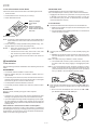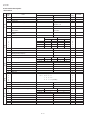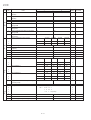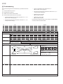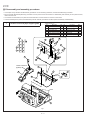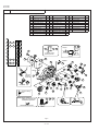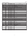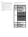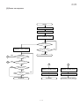
1
UX-258TH FO-475TH SERVICE MANUAL No. 00ZUX258THSME FACSIMILE UX-258 MODEL FO-475 CONTENTS CHAPTER 1. GENERAL DESCRIPTION [1] Specifications ............................................ [2] Operation panel......................................... [3] Transmittable documents .......................... [4] Installation ................................................. [5] Quick reference guide ............................... CHAPTER 5. CIRCUIT DESCRIPTION [1] Circuit description ..................................... 5-1 [2] Circuit description of control PWB ............ 5-2 [3] Circuit description of TEL/LIU PWB .......... 5-8 [4] Circuit description of power supply PWB ............................5-11 [5] Circuit description of CIS unit ...................5-11 1-1 1-2 1-3 1-4 1-7 CHAPTER 2. ADJUSTMENTS [1] Adjustments ............................................... 2-1 [2] Diagnostics and service soft switch .......... 2-2 [3] Troubleshooting ...................................... 2-17 [4] Error code table....................................... 2-18 CHAPTER 6. CIRCUIT SCHEMATICS AND PARTS LAYOUT [1] Control PWB circuit ................................... 6-1 [2] TEL/LIU PWB circuit .................................. 6-9 [3] Power supply PWB circuit ...................... 6-11 [4] Operation panel PWB circuit ................... 6-13 CHAPTER 3. MECHANISM BLOCKS [1] General description .................................. 3-1 [2] Disassembly and assembly procedures ....................................... 3-3 CHAPTER 7. OPERATION FLOWCHART [1] Protocol ..................................................... 7-1 [2] Power on sequence ................................... 7-2 CHAPTER 4. DIAGRAMS [1] Block diagram ............................................4-1 [2] Wiring diagram .......................................... 4-2 [3] Point-to-point diagram ............................... 4-3 CHAPTER 8. OTHERS [1] Service tools ............................................. 8-1 [2] IC signal name .......................................... 8-4 PARTS GUIDE Parts marked with " " is important for maintaining the safety of the set. Be sure to replace these parts with specified ones for maintaining the safety and performance of the set. SHARP CORPORATION 1-1 This document has been published to be used for after sales service only. The contents are subject to change without notice. UX-258TH FO-475TH CAUTION FOR BATTERY REPLACEMENT (Danish) ADVARSEL ! Lithiumbatteri-Eksplosionsfare ved fejlagtig håndtering. Udskiftning må kun ske med batteri af samme fabrikat og type. Levér det brugte batteri tilbage til leverandoren. (English) Caution ! Danger of explosion if battery is incorrectly replaced. Replace only with the same or equivalent type recommended by the equipment manufacturer. Discard used batteries according to manufacturer’s instructions. (Finnish) VAROITUS Paristo voi räjähtää, jos se on virheellisesti asennettu. Vaihda paristo ainoastaan laitevalmistajan suosittelemaan tyyppiin. Hävitä käytetty paristo valmistajan ohjeiden mukaisesti. (French) ATTENTION Il y a danger d’explosion s’ il y a remplacement incorrect de la batterie. Remplacer uniquement avec une batterie du même type ou d’un type recommandé par le constructeur. Mettre au rébut les batteries usagées conformément aux instructions du fabricant. (Swedish) VARNING Explosionsfare vid felaktigt batteribyte. Använd samma batterityp eller en ekvivalent typ som rekommenderas av apparattillverkaren. Kassera använt batteri enligt fabrikantens instruktion. (German) Achtung Explosionsgefahr bei Verwendung inkorrekter Batterien. Als Ersatzbatterien dürfen nur Batterien vom gleichen Typ oder vom Hersteller empfohlene Batterien verwendet werden. Entsorgung der gebrauchten Batterien nur nach den vom Hersteller angegebenen Anweisungen. 1–2 UX-258TH FO-475TH CHAPTER 1. GENERAL DESCRIPTION [1] Specifications Automatic dialing: Rapid Key Dialing: 10 numbers Speed Dialing: 20 numbers Fax paper: Initial starter roll (included with fax machine): 10 m roll Recommended replacement roll: FO-40PR 50 m roll Automatic document feeder: 10 sheets max. Effective scanning width: 210 mm max. Contrast control: Automatic/Dark selectable Copy function: Standard Telephone function: Standard (cannot be used for incoming/outgoing if power fails) Power requirements: 220-240 V, 50 Hz Paper cutting method: Automatic cutter Operating temperature: 5 to 35°C Modem speed: 9600 bps with automatic fallback to 7200, 4800, or 2400 bps Humidity: Maximum: 85 % Transmission time* : Approx. 15 seconds (Sharp special mode) Power consumption: Stand-by: 6.0 W Display: 7 x 5 dots, 1 line by 16-digit display Reception modes: TEL, FAX, TEL/FAX, ANS. Resolution: Horizontal: 8 dots/mm Vertical: Standard: 3.85 lines/mm Fine/Halftone: 7.7 lines/mm Super fine: 15.4 lines/mm Maximum: 120 W Dimensions: Width: 308 mm Depth: 256 mm Height: 138 mm Weight: * Recording system: Thermal recording Halftone (grayscale): 64 levels Applicable telephone line: Public switched telephone network/PBX Compatibility: ITU-T (CCITT) G3 mode Configuration: Half-duplex, desktop transceiver Compression scheme: MH, MR, Sharp special mode Scanning method: Sheet-feeder CIS (Contact Image Sensor) Effective recording width: 210 mm max. Input document size: Automatic feeding: Width 148 to 216 mm Length 140 to 297 mm Manual feeding: Width 148 to 216 mm Length 140 to 600 mm Approx. 2.6 kg (without attachements) Based on ITU-T (CCITT) Test Chart #1 at standard resolution in Sharp special mode, excluding time for protocol signals (i.e., ITU-T phase C time only). As a part of our policy of continuous improvement, SHARP reserves the right to make design and specification changes for procduct improvement without prior notice. The performance specifications figures indicated are nominal values of production units. There may be some deviation from these values in individual units. 1–1 UX-258TH FO-475TH [2] Operation panel 1 3 2 4 6 7 8 9 10 11 5 RECEPTION MODE FUNCTION RESOLUTION TEL FAX REC REPEAT 12 PLAY/SKIP DELETE REMINDER VOLUME DOWN TEL/FAX ANS. ABC UP DIGITAL ANSWERING SYSTEM STOP DEF SPEED DIAL JKL GHI TUV 02 03 04 05 06 07 08 09 10/POLL COPY/HELP REDIAL PQRS 01 MNO WXYZ HOL/SEARCH START/MEMORY SPEAKER 13 14 15 16 17 1. Display Press this key to select the reception mode. An arrow in the display will point to the currently selected reception mode. 14. SPEED DIAL key Press this key to dial a 2-digit Speed Dial number. 15. REDIAL key Press this key to automatically redial the last number dialed. 16. SPEAKER key 4. FUNCTION key Press this key to hear the line and fax tones through the speaker when sending a document, or dialing a voice number. Note: This is not a speakerphone. You must pick up the handset to talk with the other party. Press this key to select various special function. 5. RESOLUTION key Press this key to adjust the resolution and contrast before sending or copying a document. 17. HOLD/SEARCH key Press this key to search for an automatic dialing number, or, during a phone conversation, press this key to put the other party on hold. 6. VOLUME keys Press these keys to adjust the volume of the speaker when the SPEAKER key has been pressed, or the volume of the ringer at all other times. 18. Rapid Dial keys Press one of these keys to dial a fax or voice number automatically. (Note that you must attach the Rapid Key labels.) 7. REC key Press this key to record a phone conversation or a message. 8. REPEAT key Press this key to repeat playback of a message. 19. START/MEMORY key Press this key to send or receive a document manually when off hook. 9. PLAY/SKIP key Press this key to play recorded messages. During playback, press it to skip forward to the next message. 20 Use these keys to dial numbers, and enter number and letters during number/name storing procedures. Pull this release toward you to open the operation panel. 3. RECEPTION MODE key 19 13. Number keys This displays messages and prompts during operation and programming. 2. PANEL RELEASE 18 20. COPY/HELP key When a document is in the feeder, press this key to make a copy. At any other time, press this key to print out the Help List, a quick refernce guide to the opeation of your fax. 10. DELETE key Press this key to erase recorded messages. 11. REMINDER key Press this key to send a fax and/or voice message to another party or to yourself at a preset time. 12. STOP key Press this key to stop operations before they are completed. 1–2 UX-258TH FO-475TH [3] Transmittable documents 5. Automatic Document Feeder Capacity 1. Document Sizes Number of pages that can be placed into the feeder at anytime is as follows: Normal size width 148 – 216 mm Normal size: max. ADF 10 sheets length 140 – 297 mm Special size: single sheet only (manual feed) NOTES: (Max.) (Min.) 140mm 148mm • 600mm (Max.) A4 size 297mm When you need to send or copy more pages than the feeder limit, place additional pages in feeder when last page in feeder is being scanned. Place additional pages carefully and gently in feeder. If force is used, double-feeding or a document jam may result. 6. Readable Width & Length 216mm [Normal size] The readable width and length of a document are slightly smaller than the actual document size. 216mm [Special size] Note that characters or graphics outside the effective document scanning range will not be read. Use document carrier sheet for smaller documents. * • • With special sizes, only one sheet can be fed into the machine at a time. Insert next page into feeder as current page is being scanned. Readable width 210 mm, max. 2. Paper Thickness & Weight Thickness 2.4 x 10⁻³ –4.7 x 10⁻³ inch Normal size ADF 10 sheets Weight 0.15 x 10⁻³ lbs/inch2 Thickness 4.7 x 10⁻³ –7.9 x 10⁻³ inch Special size Weight Readable width 0.15 x 10⁻³ –0.20 x 10⁻³ lbs/inch2 3. Document Types • • Normal paper Documents handwritten in pencil (No. 2 lead or softer), fountain pen, ball-point pen, or felt-tipped pen can be transmitted. Documents of normal contrast duplicated by a copying machine can also be transmitted. • Diazo copy (blue print) • Carbon copy Readable length This is the length of the document sent minus 4 mm from the top and bottom edges. 4mm Diazo copy documents of a normal contrast may be transmitted. Readable length A carbon copy may be transmitted if its contrast is normal. 4mm 4. Cautions on Transmitting Documents • Documents written in yellow, greenish yellow, or light blue ink cannot be transmitted. • Ink, glue, and correcting fluid on documents must be dry before the documents can be transmitted. • All clips, staples and pins must be removed from documents be-fore transmission. • Patched (taped) documents should be copied first on a copier and then the copies used for transmission. • All documents should be fanned before insertion into the feeder to prevent possible double feeds. 1–3 UX-258TH FO-475TH 7. Use of Document Carrier Sheet TELEPHONE JACK A document carrier sheet must be used for the following documents. • Those with tears. A standard telephone jack must be located near the machine. This is the telephone jack commonly used in most homes and offices. • • • Those smaller than size 140 mm (W) x 140 mm (L). Carbon-backed documents Make print straight across paper E.G. Place the document carrier in the document feeder with the clear film side down Plugging the fax machine into a jack which is not an jack may result in damage to the machine or your telephone system. If you do not know what kind of jack you have, or needed to have one installed, contact the telephone company. 2. Connections 1 Connect the handset as shown and place it on the handset rest. ♦ Make sure the handset cord goes into the unmarked jack on the side of the machine! ♦ Use the handset to make ordinary phone calls, or to transmit and receive documents manually. Direction of insertion NOTE: To transmit a carbon-backed document, insert a white sheet of paper between the carbon back of the document and the document carrier. • Those containing an easily separable writing substance (e.g., tracing paper written on with a soft, heavy lead pencil). NOTES: • When using the document carrier, carefully read the instructions written on the back. • If the document carrier is dirty, clean it with a soft, moist cloth, and then dry it before using for transmission. • 2 Plug the power cord into a 220-240 V, 50 Hz, earthed (2-prong) AC outlet. ♦ Caution: Do not plug the power cord into any other kind of outlet. This will damage the machine and is not covered under the warranty. Do not place more than one document in the carrier at a time. Note: The shape of the plug is different in certain countries. [4] Installation ♦ The machine does not have a power on/off switch, so the power is turned on and off by simply plugging or unplugging the power cord. 1. Site selection Take the following points into consideration when selecting a site for this model. Note: If your area experiences a high incidence of lightning or power surges, we recommend that you install surge protectors for the power and telephone lines. Surge protectors can be purchased from your dealer or at most telephone specialty stores. ENVIRONMENT • • The machine must be installed on a level surface. • Provide easy access to the front, back, and sides of the machine. In particular, keep the area in front of the machine clear, or the original document may jam as it comes out after scanning. • • The temperature should be between 5° and 35°C. Keep the machine away from air conditioners, heaters, direct sunlight, and dust. 3 Insert one end of the telephone line cord into the "TEL. LINE" jack. The humidity should be between 30% and 85% (without condensation). Insert the other end into a standard (RJ11C) single-line telephone wall jack. ELECTRICITY ♦ Be sure to insert the telephone line cord into the "TEL. LINE" jack. Do not insert into the "TEL. SET" jack. 220-240 V, 50 Hz, earthed (2-prong) AC outlet is required. Caution! • Connection to a power source other than that specified will cause damage to the equipment and is not covered under the warranty. • If your area experiences a high incidence of lightning or power surges, we recommend that you install a surge protector for the power and telephone lines. Surge protectors can be purchased at most telephone specialty stores. If the machine is moved from a cold to a warm place... If the machine is moved from a cold to a warm place, it is possible that the reading glass may fog up, preventing proper scanning of documents for transmission. To remove the fog, turn on the power and wait approximately 2 hours before using the machine. TE SEL. T T EL LI . NE 1–4 UX-258TH FO-475TH 3 Unwrap the roll of fax paper and place it in the compartment. 3. Original document support 1 Rotate the original document support so that it points straight out. • Important: The roll must be placed so that the leading edge of the paper unrolls as shown. (The paper is only coated on one side for printing. If the roll is placed backwards, the paper will come out blank after printing.) NO! YES 4. Loading the fax paper • Your fax machine prints incoming faxes on a special kind of paper called thermal paper. • The fax’s print head creates text and images by applying heat to the thermal paper. Note: The power must be on (plug in the power cord) when loading fax paper in the fax machine. 1 Pull the release marked PANEL RELEASE toward you and open the operation panel. 4 Insert the leading edge of the paper into the paper inlet. Continue to push the paper through the inlet until it comes out of the opening in the front of the fax. Paper inlet 2 Remove the packing paper from the paper compartment. Remove cardboard and tape The paper will reappear here. Make sure it is aligned between the arrows on each side of the guide, and then passes under the plate and out the front of the fax. 5 Close the operation panel, making sure it clicks into place. Press here to close 2 Click! 1 6 A short length of the fax paper will feed out and be cut off. (If this doesn’t happen, repeat the loading procedure.) Note: The fax has a built-in anti-curl mechanism that will help to reduce paper curling problems. The anti-curl mechanism is more effective at the beginning of the paper roll and less effective towards the end. 1–5 UX-258TH FO-475TH 3 Cut off the wrinkled part of the paper. 4. Clearing a jammed document If the original document doesn’t feed properly during transmission or copying, or DOCUMENT JAMMED appears in the display, first try pressing the START/MEMORY key. If the document doesn’t feed out, open the operation panel and remove it. Important: Do not try to remove a document without opening the operation panel. This may damage the feeder mechanism. 1 Pull the release marked PANEL RELEASE toward you and open the operation panel. 4 Reload the paper. • Jammed fax paper is often caused by improper loading. Be sure to carefully follow the instructions for paper loading given in "Loading the Fax Paper" in page 1-5. 2 Remove the document. 5 If the display still shows PAPER JAMMED If the display still shows PAPER JAMMED after you press the START/ MEMORY key in Step 2 above, the cutter is still engaged in the cutting position. To open the cutter, turn the fax up on its rear end and insert any long, rod-like object with a flat or blunt end into the hole marked CUTTER RESET. Continue to push the rod in until you feel it move a lever inside the machine. 5. Clearing jammed fax paper 1 Pull the release marked PANEL RELEASE toward you and open the operation panel. TER CUT T E RES 2 Remove the paper roll. • • ABC If any pieces of paper are stuck in the cutter, remove them with caution. DEF SPEED DIAL Press the START/MEMORY key to reset the cutter. GHI JKL MNO Press this key to delete the letter highlighted by the cursor. REDIAL Press this key to move the cursor to the left. PQRS TUV WXYZ HOLD/SEARCH Press this key to change case. SPEAKER Press this key to move the cursor to the right. Press either key repeatedly to select one of the following symbols. 1–6 UX-258TH FO-475TH [5] Quick reference guide FUNCTION key menu The following chart shows the layout of the functions and settings accessed by pressing the FUNCTION key. First press the FUNCTION key, the appropriate numeric key as shown, and then "#" or " " until the desired item appears. Instructions for making each setting appear in the display. If you have any difficulty, refer to the detailed instructions on the page shown below the setting. FUNCTION 0 1 A.M. Settings Timer Mode Listing Mode Entry Mode Optional Settings Send Mode Timer List Fax/Tel Numbers for Auto Dialing Fine Resolution Priority Transaction Report Print Select Polling Mode Telephone Number List Own Number and Name Set Number of Rings To Answer Dial Mode Polling Security Select 5 Rings TEL Answer Passcode List Recall Interval Date and Time Set Recall Times Anti Junk Number Set Telephone/Fax Remote Number OGM Recording Transfer Function Toll Saver Fax Box ICM Record Time 3 2 4 Passcode List ICM Confirmation Option Setting List Remote Code On A.M. Failure Page Save Override Code Anti Junk Fax Number List Box Passcode Transfer Telephone Number Pseudo Ringing Duration Time Save Fax Signal Receive Answering Machine Program List Remote Reception Select Message List Note: Steps which are optional are enclosed in a dotted frame: Transmitting documents Normal Dialing Load document Lift handset or press SPEAKER RESOLUTION Dial (press numeric keys) START/MEMORY Wait for reception tone Direct Keypad Dialing Hang up START/MEMORY Load document RESOLUTION Dial (press numeric keys) Load document RESOLUTION Press Rapid key Load document RESOLUTION SPEED DIAL Load document RESOLUTION REDIAL Rapid Key Dialing Speed Dialing Redialing Enter Speed Dial number (press 2 numeric keys) START/MEMORY START/MEMORY Wait for reception tone Using the answering machine Recording an outgoing message FUNCTION 0 START/MEMORY Listening to received messages Erasing received messages PLAY/SKIP Press a number key to select a box: "0": General Box "1": Box 1 "2": Box 2 "3": Box 3 "4": Transfer outgoing message For a personal box, enter the box number General messages (no passcode): Hold down DELETE key for 2 seconds. Pick up the handset, press the START/MEMORY key, and then speak into the handset. Enter passcode if necessary General messages (passcode needed): Press DELETE and enter passcode. 1–7 When finished, replace the handset or press the STOP key. General messages: Press DELETE , enter box number, and enter passcode if necessary. Junk Number Check Polling UX-258TH FO-475TH 2. IC protectors replacement CHAPTER 2. ADJUSTMENTS ICPs (IC Protectors) are installed to protect the motor driver circuit. ICPs protect various ICs and electronic circuits from an overcurrent condition. [1] Adjustments The location of ICPs are shown below: General Since the following adjustments and settings are provided for this model, make adjustments and/or setup as necessary. CNPW CNLIUA 1. Adjustments FU100 Adjustments of output voltage (FACTORY ONLY) CONTROL PWB (TOP SIDE) 1. Install the power supply unit in the machine. 2. Set the recording paper and document. 3. When the document is loaded, power is supplied to the output lines. Confirm that outputs are within the limits below. (1) FU100 (ICP-S07) is installed in order to protect IC’s from an overcurrent generated in the motor drive circuit. If FU100 is open, replace it with a new one. Output voltage settings 3. Settings POWER SUPPLY PWB TEL/LIU PWB (1) Dial mode selector CNLIU CN2 DIAL mode (Soft Switch No. SWB4 DATA No. 3) (step 1) Select "OPTION SETTING". CNLIUA CNPW CONTROL PWB KEY : FUNCTION 4 DISPLAY: OPTION SETTING PRESS (step 2) Select "DIAL MODE". Output +5V +24V Voltage limits 4.75V ∼ 5.25V 23.3V ∼ 24.7V Connector No. Pin No. 1 2 3 4 5 6 7 8 9 10 CNPW KEY: # DISPLAY: DIAL MODE # # # # # # # # OR # Cursor When initially registering, the mode shows 1=TONE. When registering again, the mode which was registered formerly is shown. 1=TONE, 2=PULSE (step 3) Select, using "1" or "2". DG +5V VTH-ON MG MG MG +24V VTH VTH VTH KEY: 1 DISPLAY: TONE SELECTED KEY: 2 DISPLAY: PULSE SELECTED (step 4) End, using the "STOP" key. KEY: STOP 4. Method of release of starting lock up by Battery Reset (1) Summary There is a possibility of release of the lock up by reset the signal BATRST of CPU (FC100), if it lock up when you turn on the power of the set in UX-258 series. We inform you of the method of release. (2) Contents When you turn on the power of the set without EPROM by your mistake, if you turn off the power after, turn on the power with EPROM again, the set don’t start. In this case, before you judge the cpu (FC100) is wrong, you need to confirm the release of the lock up by reset the signal BATRST. and unknown origin in the same way. Method of the reset of signal BATRST Short the between leads of the capacitor C5 on the control PWB, X2961-81 in the state of POWER OFF. 2–1 UX-258TH FO-475TH [2] Diagnostics and service soft switch 1. Operating procedure (1) Entering the diagnostic mode Press FUNC → 9 → ROM Ver. FKD0 → 8 → # → 7 , and the following display will appear. After 2 sec: DIAG MODE FKD0 Then press the START key. Select the desired item with the key or the # key or select with the rapid key. Enter the mode with the START key. (Diag•specifications) FUNC 9 8 FKD0 7 DIAG MODE START Soft switch mode START 1 START Flash memory clear ROM & RAM check START 2 START Flash memory check Aging mode START 3 START Entry data receive Panel key test START 4 START Entry data send Check pattern mode START 5 10 START Auto feeder mode Signal send mode START 6 9 START All black mode Memory clear mode START 7 8 START Shading mode If the diag mode cannot be set, repeat the diag mode operation, performing the following operation. After the power is turned on and "ESPERE POR FAVOR" is indicated, press the STOP key. START KEY STOP KEY "Power ON" + + In relation with the process response (request from Production Engineering) "ESPERE POR FAVOR" clock indication may appear depending on STOP key timing. If the STOP key is held down, "MEMORY CLEAR?" appears. Memory clear (Work + Backup) 2. Diagnostic items ITEM DIRECT No. key 1 1 SOFT SWITCH MODE Soft switches are displayed and changed. List can be output. 2 2 ROM & RAM CHECK ROM is sum-checked, and RAM is matched. Result list is output. 3 3 AGING MODE 10 sheets of check patterns are output every 5 minutes per sheet. 4 4 PANEL KEY TEST Panel keys are tested. Result list is output. 5 5 CHECK PATTERN MODE Check pattern is output. 6 6 SIGNAL SEND MODE 7 7 MEMORY CLEAR MODE Back-up memory is cleared, and is set at delivery. 8 8 SHADING MODE Shading compensation is performed in this mode. Contents Function Various signals of FAX communication are output. 9 9 ALL BLACK MODE To check the print head, whole dots are printed over the interval of 2 m. 10 10 AUTO FEEDER MODE Insertion and discharge of document are tested. 11 − ENTRY DATA SEND Registered content is sent. 12 − ENTRY DATA RECEIVE Registered content is received, and its list is output. 13 − FLASH MEMORY CHECK Flash memory is checked. 14 − FLASH MEMORY CLEAR Data of flash memory is cleared. 2–2 UX-258TH FO-475TH 3. Diagnostic items description 3. 1. Soft switch mode 3. 6. Signal send mode The mode is used to send various signals to the circuit during FAX communication. Every push of START key sends a signal in the following sequence. Moreover, the signal sound is also output to the speaker when the line monitor of the soft switch is on. Used to change the soft switch settings. The soft switch which is stored internally is set by using the keys. The available soft switches are SW-A1 to SW-L2. [1] No signal (CML signal turned on) The content of soft switches is shown in page 2-5 to 2-16. [2] 9600bps The contents are set to factory default settings. [3] 7200bps [4] 4800bps 3. 2. ROM & RAM check [5] 2400bps ROM executes the sum check, and RAM executes the matching test. The result will be notified with the number of short sounds of the buzzer as well as by printing the ROM & RAM check list. Number of short sounds of buzzer 0 → No error 1 → ROM error 2 → RAM error (32Kbyte) [6] 300bps (FLAG) [7] 2100Hz (CED) [8] 1100Hz (CNG) [9] END 3. 3. Aging mode 3. 7. Memory clear mode If any document is first present, copying will be executed sheet by sheet. If no document is present, the check pattern will be printed sheet by sheet. This operation will be executed at a rate of one sheet per 5minutes, and will be ended at a total of 10 sheets. This mode is used to clear the backup memory and reset to the default settings. 3. 4. Panel key test The mode is used for the shooting compensation. For reading, set up the special original paper. 3. 8. Shading mode The mode is used to check whether each key operates properly or not. Press the key on the operation panel, and the key will be displayed on the display. Therefore, press all keys. At this time, finally press the STOP key. The shooting compensation memorizes the reference data of white and black for reading. Moreover, the memorized data is not erased even if memory clear mode is executed. When the STOP key is pressed, the keys which are not judged as "pressed" will be printed on the result list. • 3. 9. All black mode LED port of the contact image sensor (CIS) is kept on during the term from when start of the panel test mode to end with the STOP key. The mode is used to check the state of the printing head and intentionally overheat it. Whole dots are printed over the interval of 2 m. If it is overheated or the printing sheet is jammed, press STOP key for the end. 3. 5. Check pattern mode 3. 10. Auto feeder mode This mode is used to check the status of print head. Two sheets of check pattern are printed. The following information of check pattern is printed. 1 Vertical stripes (alternate white and black lines) 2 Full black 3 Full white In this mode, a document is inserted and discharged to check the auto feed function. Approx. 35 mm After this mode is started, set a document, and the document feed will be automatically tested. Approx. 70 mm Approx. 35 mm 3. 11. Entry data send The mode is used to send the registered data to the other machine and make the other machine copy the registered content. 1 Before sending in this mode, it is necessary to set the other machine at the entry data receive mode. The sent content is as follows. After printing is completed, the following lists are printed. 1. Telephone list data 2 2. Sender register data 3. Optional setting content 4. Soft switch content 5. Junk fax number list 3 6. Timer reservation data (only on the model which timer reservation is possible) RANK 0 or 1 Note: There is a selection RANK 0 or 1 depending on resistance value of the thermal head. RANK 0 or RANK 1 is printed at the tail of check pattern to identify. 7. Recording setting list data 2–3 UX-258TH FO-475TH 3. 12. Entry data receive 3. 13. Flash memory check In this mode, the registered data sent from the other machine are received and the received data are registered in the own machine. When this mode is used for receiving, the other machine must be in the entry data send mode. Data writing/read of flash memory is checked, and the result (OK/NG) is printed. 3. 14. Flash memory clear After receiving is completed, the following lists are printed. All data of flash memory is cleared. The result of clear (OK/NG) is printed. 1. Telephone list data 2. Sender register data (The passcode No. is also printed if the poling function is provided.) 3. Optional setting list 4. Soft switch content 5. Junk fax number list 6. Timer reservation list (only model which timer communication is possible) 7. Recording setting list data 4. How to make soft switch setting To enter the soft switch mode, make the following key entries in sequence. Press FUNCTION DATA No. 9 8 7 START START 1 2 3 4 5 6 7 8 S F T SW-A1 = 0 0 0 0 0 0 0 0 Press FUNCTION key. S F T SW-A1 = 1 0 0 0 0 0 0 0 Press key. Press key. S F T SW-A1 = 1 0 0 0 0 0 0 0 S F T SW-A1 = 1 0 0 0 0 0 0 0 Bit1 - 8 are set. S F T SW-A1 = 1 0 0 0 0 0 0 0 Press START key during setting. S F T SW-A2 = 0 0 0 0 0 0 0 0 Soft SW-A2 - SW-L2 are set. S F T SW-L2 = 0 0 0 0 0 0 0 0 To finish the settings halfway between SW-A1 and SW-L2, press the STOP key. In this case, the setting being done to the SW No. on display will be nullified while settings done to the preceding SW Nos. remain in effect. When the COPY key is pressed, the contents of soft switches are printed. The soft switch mode is terminated. 2–4 UX-258TH FO-475TH 5. Soft switch description • Soft switch SW NO. SW l A1 DATA NO. Switch setting and function ITEM 1 1 Protect from echo No Yes 0 2 Forced 4800 BPS reception Yes No 0 3 Footer print Yes No 0 4 Length limitation of copy/send/receive No limit Copy/send: 60cm 0 5 CSI transmission No transmitted Transmitted 0 6 DIS receive acknowledgement during G3 transmission Twice NSF: Once DIS: Twice 0 7 Non-modulated carrier for V29 transmission modem Yes No 0 EOL detect timer 25 s 13 s Modem speed SW l A3 V.27 ter 9600bps 7200bps 4800bps 2400bps 1 No. 1 0 0 0 0 0 2 No. 2 0 0 0 0 0 3 No. 3 0 1 1 0 0 4 No. 4 1 1 0 0 1 5 6 Sender’s information transmit H2 mode No No Yes Yes 0 0 7 Communication error treatment in RTN sending mode (reception) No communication error Communication error 0 8 CNG transmission CED tone signal interval No 1000ms Yes 750ms 500ms 75ms 0 1 No. 1 1 1 0 0 0 2 No. 2 1 0 1 0 0 3 MR coding 4 Reserved No Yes 0 5 Reserved 0 6 Reserved 0 7 Reserved 0 8 Reserved 0 1 Signal transmission level No. = 0 Binary input 0 16 8 4 2 1 0 1 0 1 0 3 4 2 3 4 5 0 1 0 0 (-8 dBm) 5 0 6 Protocol monitor (error print) Printed at com. err Not printed 0 7 Protocol monitor Yes No 0 8 Line monitor Yes No Digital line equalization setting (Reception) SW l A5 0 V.29 2 SW l A4 Remarks Receive: 1.5m 8 SW l A2 Initial setting 0 0 7.2km 0km 1 No. 1 1 0 1 2 No. 2 1 0 1 3 4 Reserved Reserved 0 0 5 Reserved 0 6 Reserved 0 7 8 Error criterion Anti junk fax check 10 ~ 20 % Yes 2–5 5 ~ 10 % No 0 0 OPTION UX-258TH FO-475TH SW NO. SW l A6 DATA NO. Switch setting and function ITEM 1 0 Initial setting 1 Auto gain control (MODEM) Enable Disable 2 End Buzzer Yes No 1 3 Disconnect the line when DIS is received in RX mode No Yes 1 4 5 Equalizer freeze control (MODEM) Equalizer freeze control 7200 BPS only On No Off Yes 0 0 6 7 CNG transmission in manual TX mode Initial compression scheme for sharp fax in Yes MR mode No H2 mode 1 0 Remarks 1 TX mode 8 Reserved 1 Recall interval 0 2 SW l B1 No. = 3 4 5 Recall times 6 No. = 7 8 SW l B2 SW l B3 SW l B4 0 2 1 1 1 2 0 1 3 0 4 1 (5 x 60 sec = 5 min) 0 1 Binary input 0 8 4 2 1 0 5 0 6 0 7 1 8 0 (Twice) 1 0 1 Dial pausing (sec/pause) 2 Reserved 3 Reserved 4 5 Busy tone detection (after auto dial) Waiting time after dialing 6 7 Reserved Reserved 0 0 8 1 Reserved Reserved 0 0 2 3 Reserved Reserved 0 0 4 Reserved 0 5 Reserved 0 6 Reserved 0 7 Reserved 0 8 Hold function Enable Disable 1 1 Auto Dial Mode Delay timer of before line connect 3 sec 0 sec 1 2 Auto Dial Mode Delay timer of after line connect 3.6 sec 3 sec 0 3 4 Dial mode Pulse → Tone change function by Tone Enable Pulse Disable 1 1 5 Dial pulse make/break ratio (%) 40/60 33/67 6 7 Reserved Reserved 0 0 8 Reserved 0 1 DTMF signal transmission level (Low) 2 3 SW l B5 Binary input 8 4 4 sec 2 sec OPTION OPTION 0 0 0 No 90 sec key Yes 45 sec No. = 1 0 1 Binary input 0 16 8 4 2 1 1 2 3 4 5 1 0 4 0 5 1 0 1 0 (0.5 x 12 = -6 dBm) 1 0 6 7 Reserved Reserved 0 0 8 Reserved 0 2–6 OPTION UX-258TH FO-475TH SW NO. DATA NO. 1 Switch setting and function ITEM 1 DTMF signal transmission level (High) 2 SW l B6 No. = Binary input 0 16 8 4 2 1 0 3 4 1 2 3 4 5 0 0 1 1 0 (0.5 x 7 = -3.5 dBm) 0 6 Reserved 0 7 8 Reserved Reserved 0 0 Factory Light Dark setting No. 1 0 1 0 1 0 2 No. 2 0 Factory 0 Light 1 Dark 1 Darker in 0 setting 3 4 0 1 0 1 0 No. 4 0 0 1 1 0 5 6 Line density selection Reserved Fine Standard 0 0 7 8 MTF correction in half tone mode Reserved No Yes 0 0 1 Number of rings for auto receive Binary input 0 8 4 2 1 0 3 1 2 3 4 0 4 0 0 0 1 (4 times) 1 No. = 5 Automatic switching manual to auto receive mode 6 Reserved 0 7 8 Reserved Reserved 0 0 1 2 Reserved Reserved 0 0 3 Reserved 0 4 5 Reserved Reserved 0 0 Reception after 5 rings CI off detection timer (Distinctive ring 6 setting off only) 7 8 1 Reserved Tel/Fax Automatic switching mode 2 switching mode 3 4 Number of CNG signal detection at the No reception 0 1200ms 1000ms 700ms 350ms No. 6 0 1 0 1 No. 7 0 0 1 1 Enable 15sec 60sec 30sec 120sec OPTION 0 0 1 1 0 0 1 0 1 0 3 sec 5 sec 1 phone/fax automatic switching mode 5 CNG detect time at TEL/FAX mode 6 7 Reserved Reserved 0 0 8 Reserved 0 2–7 OPTION 1 No. 3 Once OPTION 0 No. 2 Twice OPTION 0 0 Disable Pseudo ringing time at phone/fax automatic SW l E1 dark mode No. 3 2 SW l D2 Darker in dark mode 1 Reading slice (Half tone) SW l D1 Remarks 1 1 5 Reading slice (Binary) SW l C1 Initial setting 0 0 UX-258TH FO-475TH SW NO. Switch setting and function DATA NO. ITEM 1 Pseudo ringer sound output level to the line 1 Binary input 0 8 4 2 1 1 3 1 2 3 4 0 4 0 1 0 1 (-5 dBm -5 = -10 dBm) 1 2 SW l E2 No. = 5 Reserved 0 6 Reserved 0 7 Reserved 0 8 Reserved 0 SW l G2 SW l G3 80ms 100ms 120ms No. 1 0 0 1 1 0 2 3 No. 2 0 0 1 Protection of remote reception (5 1 No 0 0 4 Remote reception with GE telephone 5 Remote operation code figures by external 6 TEL (0~9) ) detect Yes Compatible Not compatible Binary input 0 4 2 1 1 7 5 6 7 8 8 0 1 0 1 (5 CNG detection in STAND-BY mode Yes 1 1 1pulse 2pulses 3pulses 4pulses 2 No. 2 0 0 1 1 0 3 No. 3 0 1 0 1 1 1pulse 2pulses 3pulses 4pulses 4 No. 4 0 0 1 1 0 5 6 No. 5 0 0 1 Fax signal detection after telephone mode dial 1 No 1 0 7 Reserved 0 8 Reserved 0 1 Reserved 0 2 3 Reserved Reserved 0 0 4 Reserved 0 5 6 Reserved Reserved 0 0 7 Reserved 0 8 1 Reserved Reserved 0 0 2 Reserved 0 3 Reserved 0 4 Reserved 0 5 6 Reserved Reserved 0 0 7 Reserved 0 8 Reserved 0 1 Reserved 0 2 Reserved 0 3 Reserved 0 4 Reserved 0 5 Reserved 0 6 7 Reserved Reserved 0 0 8 Reserved 0 Yes 2–8 OPTION 0 ) No Number of CNG (STAND-BY mode) OPTION 1 8 No. = Number of CNG detect (AM mode) SW l G1 50ms 1 1 SW l F2 Remarks (-5 ~ -20 dBm setting) DTMF detection time SW l F1 Initial setting 0 OPTION UX-258TH FO-475TH SW NO. SW l H1 DATA NO. Switch setting and function ITEM 1 Initial setting 0 1 Busy tone detection ON/OFF time (Lower duration) 350ms 150ms 0 2 Busy tone detection ON/OFF time (Upper duration) 650ms 900ms 0 3 Reserved 4 Busy tone continuous sound detect time 5s 10s 1 5 Busy tone detect continuation sound detect No Yes 0 6 during OGM Busy tone detect continuation sound detect No Yes 0 No Yes 0 No Yes 0 Remarks 0 during ICM 7 Busy tone detect intermittent sound detect during OGM 8 Busy tone detect intermittent sound detect during ICM Busy tone detection pulse number SW l H2 4pulses 6pulses 10pulses 1 No. 1 0 0 1 1 2 No. 2 0 1 0 1 0 1 3 Fax switching when A.M. full Yes No 0 4 Busy tone detect continuation sound detect 320 - 570 Hz 320 - 460 Hz 0 5 Reserved 0 6 Reserved 0 7 Reserved 0 8 Reserved 0 1 No. 1 2 No. 2 A.M. quiet time 1 4min 15s 30s 60s 0 0 1 1 0 0 0 1 0 1 2S 3s 4s 5s OPTION 3 No. 3 0 0 1 1 0 4 No. 4 0 0s 1 1s 0 2s 1 3s 0 5 No. 5 0 0 1 1 1 6 7 No. 6 0 1 Off 0 1 0 0 A.M. quiet time 2 Key input buzzer on/off switch (Two way On recording mode) 8 Reserved 1 A.M. quiet detect time 0 2 SW l I2 OPTION frequency ICM recording time SW l I1 2pulses No. = Binary input 0 16 8 4 2 1 0 3 1 2 3 4 5 1 4 5 0 0 1 1 0 (6 sec) 1 0 6 Reserved 7 Reserved 8 Alarm during two way recording 0 0 Yes No 2–9 0 UX-258TH FO-475TH SW NO. SW l I3 SW l I4 DATA NO. Switch setting and function ITEM 1 1 Max OGM record time 2 Reserved 15s 60s 3 Two way record function Disable Enable 0 4 Toll saver Disable Enable 0 5 Reserved 0 6 Reserved 0 7 BOX selection to record ICM 2 digits DTMF 1digit DTMF 0 8 Transfer did recall Disable Enable 0 1 2 AGC maximum gain (line) (10 ~ 25 dBm ) No. = Binary input 8 4 2 1 1 2 3 4 0 AGC maximum gain (Mic) 1 1 0 1 (23 dB) Binary input 1 0 6 (10 ~ 25 dBm ) No. = AGC eref access code (line) (-0 ~ -30 dBm with 2 dBm step) No. = 4 5 6 8 4 2 1 0 5 6 7 8 0 0 1 0 1 0 No. = 0 8 4 2 1 1 2 3 4 1 1 1 1 0 5 6 7 8 0 8 1 AGC again adaptation threshold (line) 1 0 0 1 (-18 dB) Binary input 1 1 2 (-40 ~ -70 dBm with 2 dBm step) 8 4 2 1 1 No. = 3 4 1 2 3 4 1 1 1 1 5 AGC again adaptation threshold (Mic) 6 7 (-40 ~ -70 dBm with 2 dBm step) No. = 1 1 (-70 dB) Binary input 0 8 4 2 1 5 6 7 8 1 0 0 1 0 1 (-50 dB) Slow 0 Normal 0 Little fast 1 Fast 1 AGC slew rate (line) 1 1 No. 1 2 No. 2 0 Slow 1 Normal 0 Little fast 1 Fast 1 No. 3 0 0 1 1 1 0 1 Enable 0 1 1 0 AGC slew rate (Mic) 3 4 5 FAX BOX function No. 4 Disable 6 Frequency of voice detection after 800 Hz ~ 1400 Hz REMINDER dialing Voice detection time after REMINDER dialing SW l J1 (-14 dB) Binary input 8 4 2 1 7 8 SW l I7 (12 dB) Binary input 0 1 1 1 AGC eref access code (Mic) (-0 ~ -30 dBm with 2 dBm step) OPTION 1 1 4 5 2 3 SW l I6 0 3 1 Remarks 0 7 8 SW l I5 Initial setting 0 800 Hz ~ 1200 Hz 0 OPTION 0 100ms 200ms 300ms 400ms 7 No. 7 0 0 1 1 8 No. 8 0 1 0 1 0 0 1 Reserved 0 2 Reserved 3 Sender’s phone number setting 4 5 Reserved Reserved 0 0 6 Reserved 0 0 Cannot change Ringer volume Change allowed 0 7 No. 7 Off 0 Low 0 Middle 1 High 1 1 8 No. 8 0 1 0 1 0 2 – 10 OPTION UX-258TH FO-475TH SW NO. SW l J2 DATA NO. Switch setting and function ITEM 1 Reserved 2 Reserved 3 Polling key 4 Reserved 5 Reserved 1 0 Yes 2 Reserved 3 Communication results printout (Transaction report) 0 Very Low Low Middle High Very High No. 6 No. 7 0 0 0 0 0 1 0 1 1 0 No. 8 0 1 0 1 0 OPTION 0 1 0 0 0 No. 3 4 Error/Timer Send only 0 0 No. 4 0 1 Always 1 No print 1 0 1 OPTION 0 0 5 6 Reserved Reserved 0 0 7 Reserved 0 8 1 Reserved Entering DIAG mode by pressing SPEED 2 Reserved 0 3 Reserved 0 4 Reserved 0 5 Reserved 0 6 Reserved 0 7 Reserved 0 8 Reserved Yes No 0 0 key SW l K1 0 OGM / ICM output level 1 SW l L1 SW l L2 OPTION 0 8 SW l J3 NO 0 6 7 Reserved Remarks 0 Speaker volume (5 stages) 1 Initial setting 0 Binary input No. = 16 8 4 2 1 2 3 1 2 3 4 5 1 0 0 0 1 (-17 dBm) 1 0 0 4 0 5 1 6 Reserved 0 7 8 Reserved Reserved 0 0 1 Reserved 0 2 Reserved 0 3 Reserved 0 4 Reserved 0 5 6 Reserved Reserved 0 0 7 Reserved 0 8 Reserved 0 2 – 11 UX-258TH FO-475TH • Soft switch function description SW-A2 No. 7 Communication error treatment in RTN sending mode (Reception) SW-A1 No. 1 Protect from echo Used to determine communication error treatment when RTN is sent by occurrence of a received image error in G3 reception. When it is set to "1", communication error is judged as no error. Used to protect from echo in reception. SW-A1 No. 2 Forced 4800BPS reception SW-A2 No. 8 CNG transmission When line conditions warrant that receptions take place at 4800 BPS repeatedly. When set to "0" , this model allows CNG transmission by pressing the Start key in the key pad dialing mode. When set to "1", CNG transmission in the key pad dialing mode cannot be performed. In either case, CNG transmission can be performed in the auto dial mode. It may improve the success of receptions by setting at 4800BPS. This improve the receiving document quality and reduces handshake time due to fallback during training. SW-A3 No. 1, No. 2 CED tone signal interval SW-A1 No. 3 Footer print For international communication, the 2100Hz CED tone may act as an echo suppression switch, causing a communication problem. When set to "1", the date of reception, the sender machine No., and the page No. are automatically recorded at the end of reception. Though SW-A3 No. 1 and No. 2 are normally set to 0, it should be changed this time between the CED tone signal to eliminate the communication problem caused by echo. SW-A1 No. 4 Length limitation of copy/send/receive Used to set the maximum page length. TX To avoid possible paper jam, the page length is normally limited to 0.6 meter for copy or transmit, and 1.5 meters for receive. RX CED It is possible to set it to "No limit" to transmit a long document, such as a computer print form, etc. (In this case, the receiver must also be set to no limit.) T DIS SW-A1 No. 5 CSI transmission (CSI TRANSMISSION) is a switch to set whether the machine sends or does not send the signal (CSI signal) informing its own telephone No. to the remote fax. machine when information is received. When "nonsending" is set, the telephone No. is not output on the remote transmitting machine if the remote transmitting machine has the function to display or print the telephone No. of receiving machine, using this CSI signal. SW-A3 No. 3 MR Coding Used to select the MR coding enable or disable. SW-A3 No. 4 ~ No. 8 Reserved Set to "0". SW-A4 No. 1 ~ No. 5 Signal transmission level SW-A1 No. 6 DIS receive acknowledgment during G3 transmission Used to control the signal transmission level in the range of-0dB to31dB. Used to make a choice of whether reception of DIS (NSF) is acknowledged after receiving two DISs (NSFs) or receiving one DIS (two NSFs). It may be useful for overseas communication to avoid an echo suppression problem, if set to 1. The factory setting is at -8dB (MODEM output). SW-A4 No. 6 Protocol monitor (Error print) If set to "1", protocol is printed at communication error. SW-A1 No. 7 Non-modulated carrier for V29 transmission modem SW-A4 No. 7 Protocol monitor Though transmission of a non-modulated carrier is not required for transmission by the V29 modem according to the CCITT recommendation, it may be permitted to a send non-modulated carrier before the image signal to avoid and echo suppression problem. It may be useful for overseas communication to avoid an echo suppression problem, if set to 1. Normally set to "0". If set to "1", communication can be checked, in case of troubles, without using a G3 tester or other tools. When communication FSK data transmission or reception is made, the data is taken into the buffer. When communication is finished, the data is analyzed and printed out. When data is received with the line monitor (SW-A4 No. 8) set to "1" the reception level is also printed out. SW-A1 No. 8 EOL (End Of Line) detect timer Used to make a choice of whether to use the 25-second or 13-second timer for detection of EOL. This is effective to override communication failures with some facsimile models that have longer EOL detection. SW-A4 No. 8 Line monitor Normally set to "0". If set to "1", the transmission speed and the reception level are displayed on the LCD. Used for line tests. SW-A2 No. 1 ~ No. 4 Modem speed SW-A5 No. 1, No. 2 Digital line equalization setting (Reception) Used to set determine the initial modem speed. The default is 9600BPS. It may be necessary to program it to a slower speed when frequent line fallback is encountered, in order to save the time required for fallback procedure. Line equalization when reception is to be set according to the line characteristics. Setting should be made according to distance between the telephone and the telephone company central switching station. SW-A2 No. 5 Sender’s information transmit SW-A5 No. 3 ~ No. 6 Reserved (SENDER’S INFORMATION TRANSMISSION) is a switch to set the function to print the content of HEADER PRINT described in the passcode list at the front end of receiver’s original when original is sent to the remote machine. Set to "0". SW-A5 No. 7 Error criterion Used to select error criterion for sending back RTN when receiving image data. If this switch is set to "NO", the HEADER PRINT is not output at the receiving machine. SW-A5 No. 8 Anti junk fax check SW-A2 No. 6 H2 mode When use the Anti junk fax function, set to "1". Used to determine reception of H2 mode (15 sec transmission mode). When set to OFF, H2 mode reception is inhibited even though the transmitting machine has H2 mode function. SW-A6 No. 1 Auto gain control (MODEM) When this mode is enabled, if the reception signal level is under 31dBm. The modem itself controls the signal gain automatically. 2 – 12 UX-258TH FO-475TH SW-A6 No. 2 End buzzer SW-B4 No. 2 Auto dial mode Delay timer of after line connect Setting this bit to 0 will disable the end buzzer (including the error buzzer/ on-hook buzzer). Delay time between the line connection and dial data output under the auto dial mode. DIAL DATA SW-A6 No. 3 Disconnect the line when DIS is received in RX mode RAPID01 CML RELAY ON Bit1= 0: When DIS signal is received during RX mode, disconnected the line is immediately. Bit1= 1: When DIS signal is received during RX mode, wait the next signal. 0 : 3 sec 1 : 3.6 sec SW-B4 No. 3 Dial mode SW-A6 No. 4 Equalizer freeze control (MODEM) When using the pulse dial, set to 0. When using the tone dial, set to 1. SW-B4 No. 4 Pulse → Tone change function by key When setting to 1, the mode is changed by pressing the key from the pulse dial mode to the tone dial mode. This switch is used to perform reception operation by fixing the equalizer control of modem for the line which is always in unfavorable state and picture cannot be received. * Usually, the control is executed according to the state of line where the equalizer setting is changed always. SW-B4 No. 5 Dial pulse make/break ratio (%) When using the 33 % make ratio pulse dial, set to "0". When using the 40 % make ratio pulse dial, set to "1". SW-A6 No. 5 Equalizer freeze control 7200BPS only Setting which specifies SW-A3 No. 6 control only in the condition of 7200BPS modem speed. SW-B4 No. 6 ~ No. 8 Reserved SW-A6 No. 6 CNG transmission in manual TX mode Set to "0". When set to "1", fax transmit the CNG signal in case of manual transmission mode (User press the START key after waiting the fax answering signal from handset or speaker). SW-B5 No. 1 ~ No. 5 DTMF signal transmission level (Low) The transmission level of DTMF signal is adjusted. (lower frequency) 00000: 0dBm SW-A6 No. 7 Initial compression scheme for sharp fax in TX mode ↓ When set to "0", if the other fax is Sharp model, fax transmit the document by H2 mode. When set to "1", even if the other fax is Sharp model, fax transmit the document by MR mode. 11111: -15.5dBm (-0.5dBm x 31) SW-B5 No. 6 ~ No. 8 Reserved SW-A6 No. 8 Reserved Set to "0". Set to "0". SW-B6 No. 1 ~ No. 5 DTMF signal transmission level (High) SW-B1 No. 1 ~ No. 4 Recall interval The transmission level of DTMF signal is adjusted. (higher frequency) Choice is made for a redial interval for speed and rapid dial calls. Used a binary number to program this. If set to 0 accidentally, 1 will be assumed. 00000: 0dBm SW-B1 No. 5 ~ No. 8 Recall times 11111: -15.5 dBm (-0.5dBm x 31) ↓ Choice is made as to how many redials should be. SW-B6 No. 6 ~ No. 8 Reserved SW-B2 No. 1 Dialing pause (sec/pause) Set to "0". Pauses can be inserted between telephone numbers of direct dial connection. Selection of 4 sec or 2 sec pause is available. SW-C1 No. 1, No. 2 Reading slice (Binary) SW-B2 No. 2, No. 3 Reserved Used to determine the set value of reading density in standard/fine mode. The standard setting is "00" (Factory setting is "00") Set to "0". SW-C1 No. 3, No. 4 Reading slice (Half tone) SW-B2 No. 4 Busy tone detection (after auto dial) Used to determine the set value of reading density in half tone mode. The standard setting is "00" (Factory setting is "00") Used to set YES/NO of busy tone detection after auto dialing. SW-C1 No. 5 Line density selection SW-B2 No. 5 Waiting time after dialing Used to set the transmission mode which is automatically selected when the Resolution key is not pressed. In the copy mode, however, the fine mode is automatically selected unless the Resolution key is manually set to another mode. This is waiting time for the opponent’s signals after dialing. When set to "0", waiting time is 45 sec. When set to "1", waiting time is 90 sec. SW-C1 No. 6 Reserved SW-B2 No. 6 ~ No. 8 Reserved Set to "0". Set to "0". SW-C1 No. 7 MTF correction in half tone mode SW-B3 No. 1 ~ No. 7 Reserved This allows selection of MTF correction (dimness correction) in the half tone mode. When "NO" (=1) is selected, the whole image becomes soft and mild. On the contrary, however, clearness of characters will be reduced. Normally set to "YES" (=0). Set to "0". SW-B3 No. 8 Hold function Used to set YES/NO of holding function by the HOLD key. SW-B4 No. 1 Auto dial mode Delay timer of before line connect SW-C1 No. 8 Reserved Delay time between the dial key input and line connection under the auto dial mode. RAPID01 Set to "0". CML RELAY ON DIALLING 0 : 0sec 1 : 3sec 2 – 13 UX-258TH FO-475TH SW-D1 No. 1 ~ No. 4 Number of rings for auto receive SW-F1 No. 3 Protection of remote reception (5 When the machine is set in the auto receive mode, the number of rings before answering can be selected. It may be set from one to nine rings using a binary number. Since the facsimile telephone could be used as an ordinary telephone if the handset is taken off the hook, it should be programmed to the user’s choice. If the soft switch was set to 1, direct connection is made to the facsimile. If a facsimile calling beep was heard when the handset is taken off the hook, press the START key and put the handset on the hook to have the facsimile start receiving. If it was set to 0 accidentally, receive ring is set to 1. NOTE: If the machine is set to answer after a large number of rings, it may not be able to receive faxes successfully. If you have difficulty receiving faxes, reduce the number of rings to a maximum of 5. Used to set the function of remote reception (5 the remote reception function is disabled. ) detect ). When set to "1", SW-F1 No. 4 Remote reception with GE telephone (Corresponding to TEL made by GE) P. B. X. "1": Compatible with TEL mode by GE "0": Not compatible SW-D1 No. 5 Automatic switching manual to auto receive mode This soft switch is used to select whether the machine should switch to the auto receive mode after 5 rings in the manual receive mode or remain in the same way as SW-D1 No. 1, No. 2, No. 3 and No. 4 "0"1"0"1"(5 rings). • When sending (5 ) for remote reception with a GE manufactured telephone remote reception may not take place because of special specifications in their DTMF. To overcome this, a soft SW is provided to change the modem setting to allow for remote reception. • If this soft SW is set to "1", other telephone sets may be adversely affected. SW-F1 No. 5 ~ No. 8 Remote operation code figures by external TEL (0 ~ 9) Remote operation codes can be changes from 0 through 9. If set to greater than 9, it defaults to 9. The "5 " is not changed. Ex-7 (Default: 5 ) SW-D1 No. 6 ~ No. 8 Reserved Set to "0". SW-D2 No. 1 ~ No. 5 Reserved SW-F2 No. 1 CNG detection in STAND-BY mode Set to "0". When setting to "1", the CNG signal detection function during standby stops. SW-D2 No. 6, No. 7 CI off detection timer (Distinctive ring setting off only) SW-F2 No. 2, No. 3 Number of CNG detect (AM mode) Set the minimum time period of CI signal interruption which affords to be judged as a CI OFF section. A Used for detection of CNG in 1 to 4 pulses. SW-F2 No. 4, No. 5 Number of CNG (STAND-BY mode) B Used for detection of CNG in 1 to 4 pulses. 1 400msec SW-F2 No. 6 Fax signal detection after telephone mode dial 2 2000msec When set to "1", if machine detect the fax answering signal after telephone calling (handset off-hook or speaker mode dial), machine start to receive the documents automatically. SW-D2 No. 8 Reserved Set to "0". SW-F2 No. 7, No. 8 Reserved SW-E1 No. 1 Tel/Fax Automatic switching mode Set to "0". Used to set auto TEL/FAX switching mode or to set the normal fax mode. SW-G1 No. 1 ~ No. 8 Reserved SW-E1 No. 2, No. 3 Pseudo ringing time at the phone/fax automatic switching mode Set to "0". Choice is made as to how long to rumble the dummy ringer on TEL/FAX automatic switching mode. Set to "0". SW-G2 No. 1 ~ No. 8 Reserved SW-E1 No. 4 Number of CNG signal detection at the phone/fax automatic switching mode SW-G3 No. 1 ~ No. 8 Reserved Used for detection of CNG in one tone or two tones in the TEL/FAX automatic switching mode. SW-H1 No. 1 Busy tone detection ON/OFF time (Lower duration) Set to "0". The initial value of detection is set according to electric condition. SW-E1 No. 5 CNG detect time at TEL/FAX mode The set value is changed according to the local switch board. (Erroneous detection of sound is reduced.) The switch which sets the time from the start of CNG detection to the end of detection. Normally the upper limit is set to 900msec, and the lower limit to 150msec. SW-E1 No. 6 ~ No. 8 Reserved Set to "0". If erroneous detection is caused by sound, etc., adjust the detection range. SW-E2 No. 1 ~ No. 4 Pseudo ringer sound output level to the line The lower limit can be set in the range of 350msec to 150msec. Used to adjust sound volume of pseudo ringer to the line (ring back tone) generated on selecting TEL/FAX. Setting is the reduce level from -5 dBm output level. SW-H1 No. 2 Busy tone detection ON/OFF time (Upper duration) Similarly to SW-H1 No. 1, the set value can be varied. The upper limit can be set in the range of 650msec to 900msec. SW-E2 No. 5 ~ No. 8 Reserved Set to "0". SW-H1 No. 1 SW-H1 No. 2 Detection range SW-F1 No. 1, No. 2 DTMF detect time 0 0 150msec ~ 900msec Used to set detect time of DTMF (Dual Tone Multi Frequency) used in remote reception (5 ). 0 1 150msec ~ 650msec 1 0 350msec ~ 900msec The longer the detect time is, the less the error detection is caused by noises. 1 1 350msec ~ 650msec 2 – 14 UX-258TH FO-475TH SW-H1 No. 3 Reserved SW-I2 No. 8 Alarm during two way recording Set to "0". When set to “1”, alarm sound is given to remote side during two way recording. SW-H1 No. 4 Busy tone continuous sound detect time SW-I3 No. 1 Max OGM record time Set detecting time busy tone continuous sound for 5 seconds or 10 seconds. Used to select the maximum OGM recording time (1 = 15 sec, 0 = 60 sec). SW-H1 No. 5 Busy tone detect continuation sound detect during OGM SW-I3 No. 2 Reserved Used to detect the continuous tone of specific frequency during OGM output. Set to “0”. SW-H1 No. 6 Busy tone detect continuation sound detect during ICM If this switch is set to “1”, machine doesn’t work two way recording function. Used to detect the continuous tone of specific frequency during ICM recording. SW-I3 No. 4 Toll saver SW-I3 No. 3 Two way record function Used to turn on the toll saver function. If it is off, the reception frequency in the AM mode is identical with that in the FAX mode. SW-H1 No. 7 Busy tone detect intermittent sound detect during OGM Used to detect the intermitten tone of specific frequency during OGM output. SW-I3 No. 5, No. 6 Reserved SW-H1 No. 8 Busy tone detect intermittent sound detect during ICM SW-I3 No. 7 BOX selection to record ICM Set to “0”. This switch is selection to digit of BOX selection code (DTMF code). Used to detect the intermittent tone of specific frequency during ICM recording. 1-digit: Input of box number (1-3) 2-digit: Input of box number (01-03) SW-H2 No. 1, No. 2 Busy tone detection pulse number Note: In case of 1-digit, the DTMF code can be accepted for 4 seconds from the beginning of ICM. Used to set detection of Busy tone intermittent sounds. OGM OUT PUT MAX 60S SW-H2 No. 3 Fax switching when A.M. full If the answering machine’s memory (tape) is full and there is no response, the machine automatically switches to Fax reception. 1 digit SW-H2 No. 4 Busy tone detect continuation sound detect frequency 2 digit BEEP 1S ICM RECORDING 4S For 4 seconds from the beginning of ICM OGM/ICM Set detecting frequency of busy tone continuation sound for 320 ~ 570 Hz or 320 ~ 460 Hz. SW-I3 No. 8 Transfer dial recall SW-H2 No. 5 ~ No. 8 Reserved If this switch is set to “1”, machine disable redial in Transfer function. Set to "0". SW-I4 No. 1 ~ No. 4 AGC maximum gain (Line) (10~25dBm) SW-I1 No. 1, No. 2 ICM recording time The AGC Maximum Gain limits the gain applied by the AGC. Message with average energy below the AGC Energy Reference Level will have their average energy level increased by no more than the AGC Maximum Gain. The AGC Maximum Gain should average energy of the message with the lowest average energy to the AGC Energy Reference Level. Used to select the incoming message recording time among 15sec/ 30sec/60sec/4min. SW-I1 No. 3, No. 4 A.M. quiet time 1 Used to select four kinds of no sound time (2 sec ~ 5 sec) after reception in the T. A. D mode until OGM is output. Reception OGM output SW-I4 No. 5 ~ No. 8 AGC maximum gain (Mic) (10~25dBm) ICM recording The AGC Maximum Gain limits the gain applied by the AGC. Message with average energy below the AGC Energy Reference Level will have their average energy level increased by no more than the AGC Maximum Gain. The AGC Maximum Gain should average energy of the message with the lowest average energy to the AGC Energy Reference Level. 2 sec~ 5 sec ( SW-I1No. 3, No. 4) SW-I1 No. 5, No. 6 A.M. quiet time 2 Used to select four kinds of no sound time (0 sec ~ 3 sec) after OGM output the T. A. D mode until ICM recording is started. Reception OGM output SW-I5 No. 1 ~ No. 4 AGC eref access code (Line) (-0~-30dBm with 2dBm step) ICM recording The AGC Energy Reference Level controls the playback level. Any message having average speech energy above the energy reference level has its playback level attenuated, and any level has its playback level increased. If the playback level is too high (low), then decreasing (increasing) the AGC energy Reference level will achieve the desired level. 0 sec~3 sec (SW-I1 No. 5, No. 6) SW-I1 No. 7 key input buzzer on/off switch (Two way recording mode) Used to turn ON/OFF key input buzzer in the TWO-WAY recording mode. SW-I5 No. 5 ~ No. 8 AGC eref access code (Mic) (-0~-30dBm with 2dBm step) SW-I1 No. 8 Reserved The AGC Energy Reference Level controls the playback level. Any message having average speech energy above the energy reference level has its playback level attenuated, and any level has its playback level increased. If the playback level is too high (low), then decreasing (increasing) the AGC energy Reference level will achieve the desired level. Set to “0”. SW-I2 No. 1 ~ No. 5 A.M. quiet detect time Used to set no sound time (0 sec - 32 sec) during the T. A. D. mode operation. SW-I2 No. 6, No. 7 Reserved Set to “0”. 2 – 15 UX-258TH FO-475TH SW-I6 No. 1 ~ No. 4 AGC gain adaptation threshold (Line) (-40~-70dBm with 2dBm step) SW-J1 No. 1, No. 2 Reserved Set to "0". The AGC adjusts the amount of gain applied to the incoming message only when the average energy exceeds the AGC Gain Adaptation Threshold. The AGC Gain Adaptation Threshold prevents message background noise from corrupting the gain provided that the AGC Gain Adaptation Threshold is greater than the background noise energy. In the event that a message has background noise energy greater than the AGC Gain Adaptation Threshold, the AGC Gain can be no greater than the AGC Maximum Gain. Note that the AGC Gain Adaptation Threshold must always be greater than the RPACS VOX Turn-On Threshold). SW-J1 No. 3 Sender’s phone number setting Used to make a choice of whether the registered sender’s phone number can be changed or not. If the switch is set to "1", new registration of the sender’s phone number is disabled to prevent accidental wrong input. SW-J1 No. 4 ~ No. 6 Reserved Set to "0". SW-J1 No. 7, No. 8 Ringer volume Used to adjust ringing volume. SW-I6 No. 5 ~ No. 8 AGC gain adaptation threshold (Mic) (-40~-70dBm with 2dBm step) SW-J2 No. 1, No. 2 Reserved Set to "0". The AGC adjusts the amount of gain applied to the incoming message only when the average energy exceeds the AGC Gain Adaptation Threshold. The AGC Gain Adaptation Threshold prevents message background noise from corrupting the gain provided that the AGC Gain Adaptation Threshold is greater than the background noise energy. In the event that a message has background noise energy greater than the AGC Gain Adaptation Threshold, the AGC Gain can be no greater than the AGC Maximum Gain. Note that the AGC Gain Adaptation Threshold must always be greater than the RPACS VOX Turn-On Threshold. SW-J2 No. 3 Polling key If this switch is set to 1, the last of Rapid key works as polling key. SW-J2 No. 4, No. 5 Reserved Set to "0". SW-J2 No. 6 ~ No. 8 Speaker volume (5 stages) Used to adjust sound volume from a speaker. SW-J3 No. 1, No. 2 Reserved SW-I7 No. 1, No. 2 AGC slew rate (Line) Set to "0". The AGC Slew Rate controls the convergence of the message playback level to the desired playback level. A large slew rate will allow faster convergence and a small slew rate will allow slower convergence. SW-J3 No. 3, No. 4 Communication result printout (Transaction report) It is possible to obtain transaction results after each communication. Normally, the switch is set (No. 1: 0, No. 2: 0) so that the transaction report is produced only when a communication error is encountered. If No. 1 was set to 1 and No. 2 to 0, the transaction report will be produced every time a communication is done, even if the communication was successful. Setting No. 1 to 1 and No. 2 to 1 will disable this function. No transaction report printed. SW-I7 No. 3, No. 4 AGC slew rate (Mic) The AGC Slew Rate controls the convergence of the message playback level to the desired playback level. A large slew rate will allow faster convergence and a small slew rate will allow slower convergence. SW-I7 No. 5 FAX BOX function FAX BOX function YES/NO is set. SW-J3 No. 5 ~ No. 8 Reserved Energy reference threshold Output Gain (dB) adaptive threshold Set to "0". SW-K1 No. 1 Entering DIAG mode by pressing SPEED key Maximum gain A bit which is used in the production process only. When the SPEED key is pressed, the switch is changed from the stand-by state to the DIAG mode. SW-K1 No. 2 ~ No. 8 Reserved Set to "0". Energy Energy Gain adaptive reference reference threshold threshold threshold (...Maximum gain) Input(dB) SW-L1 No. 1 ~ No. 5 OGM/ICM output level Energy reference threshold (...+25dB) Used to control OGM and ICM output level. SW-L1 No. 6 ~ No. 8 Reserved Set to "0". SW-L2 No. 1 ~ No. 8 Reserved RPACS AGC Parameter operation envelope Set to "0". SW-I7 No. 6 Frequency of voice detection after REMINDER dialing When reminder calling, machine will detect the voice signal and start to send the reminder voice message. This switch is used to select the voice detecting frequency range. When set to "0", machine detect the 800 ~ 1200 Hz as voice. When set to "1", machine detect the 800 ~ 1400 Hz as voice. SW-I7 No. 7, No. 8 Voice detection time after REMINDER dialing This switch is used how long time coming voice frequency is judged as voice. 2 – 16 UX-258TH FO-475TH [3] Troubleshooting Refer to the following actions to troubleshoot any of problems mentioned in 1-4. [1] A communication error occurs. [2] Image distortion produced. [3] Unable to do overseas communication. [4] Communication speed slow due to FALLBACK. • Increase the transmission level SOFT SWITCH A4-1, 2, 3, 4, 5. May be used in case [1] [2] [3]. • Decrease the transmission level SOFT SWITCH A4-1, 2, 3, 4, 5. May be used in case [3]. • Apply line equalization SOFT SWITCH A5-1, 2. May be used in case [1] [2] [3] [4]. • Slow down the transmission speed SOFT SWITCH A2-1, 2, 3, 4. May be used in case [2] [3]. • Replace the TEL/LIU PWB. May be used in all cases. • Replace the control PWB. May be used in all cases. * If transmission problems still exist on the machine, use the following format and check the related matters. TO: ATT: Ref.No. : CC: ATT: Date : Dept : Sign : FM: From: Mr. Our customer Other party Problem mode Name Address Contact person Name Address Contact person Line: Domestic / international Reception / Transmission Frequency: Confirmation item Ref.No.: ***** Facsimile communication problem ***** Fax Tel No.: Our customer Date: Model: G3 Automatic reception / Manual reception Automatic dialing / Manual dialing / Others % ROM version: Other party B1 B2 Tel No. Fax No. Model name Tel No. Fax No. Model name Phase: A, B, C, D. Please mark problem with an X. No problem is: 0. A1 A2 B1 B2 C1 C2 A1 A2 C1 D2 C2 E1 E2 Our service D1 Other party's service Comment Countermeasure **** Please attach the G3 data and activity report on problem. **** * Please complete this report before calling the “TAC” hotline if problem still occurs. 2 – 17 D1 D2 E1 E2 Transmission level setting is ( customer Transmission level ( ) dBm Reception level ( ) dBm By level meter at B1 and B2 ) dB at our UX-258TH FO-475TH [4] Error code table 1. Communication error code table G3 Transmission Code Final received signal Error Condition (Receiver side) 0 Incomplete signal frame Cannot recognize bit stream after flag 1 NSF, DIS Cannot recognize DCS signal by echo etc. 2 CFR Disconnects line during reception (carrier missing etc) 3 FTT Disconnects line by fall back 4 MCF Cannot recognize NSS signal (FIF code etc) Disconnects line during reception of multi page Cannot recognize NSS, DCS signal in the case of mode change 5 PIP or PIN The line is hung up without replying to telephone request from the receiving party. 6 RTN or RTP Cannot recognize NSS, DCS signal after transmit RTN or RTP signal. 7 8 No signal or DCN − No response in receiver side or DCN signal received* (transmitter side) Owing to error in some page the error could not be corrected although the specified number of error retransmission was at tempted. 11 − 12 − Error occurred just after fallback. 13 − Error occurred after a response to retransmission end command was received. Error occurred after or while reception by the remote (receiving) machine was revealed to be impossible. G3 Reception Code 0 1 Final received signal Incomplete signal frame NSS, DCS Error Condition (Receiver side) Cannot recognize bit stream after flag Cannot recognize CFR or FTT signal Disconnects line during transmission (line error) 2 NSC, DTC Cannot recognize NSS signal (FIF code etc) 3 EOP Cannot recognize MCF, PIP, PIN, RTN, RTP signal 4 5 EOM MPS Cannot recognize MCF, PIP, PIN, RTN, RTP signal in the case of mode change The line is hung up without replying to communication request. 6 7 PR1-Q No signal or DCN Cannot recognize PIP, PIN signal in the case of TALK request No response in transmitter (cannot recognize DIS signal) or DCN signal received* (receiver side) 8 − Error occurred upon completion of reception of all pages. 9 − Error occurred when mode was changed or Transmission/Reception switching was performed. 10 − Error occurred during partial page or physical page reception. 11 − Error occurred after or during inquiry from the remote (transmitting) machine as to whether 12 − Error occurred during or just after fallback. 13 − Error occurred after the retransmission end command was received. reception is possible or not. 2 – 18 UX-258TH FO-475TH 3-2. Automatic document feed CHAPTER 3. MECHANISM BLOCKS 1) Use of the paper feed roller and separation rubber plate ensures error-free transport and separation of documents. The plate spring presses the document to the paper feed roller to assure smooth feeding of the document. [1] General description 2) Document separation method: Separation rubber plate 1. Document feed block and diagram Separator rubber Paper feed spring Separator rubber Paper feed spring Rear roller A/B Transfer roller Document Document Paper feed roller Paper feed roller CIS Pinch roller Fig. 3 3-3. Documents applicable for automatic feed Fig. 1 Square meter series 4x6 series (788mm x 1091mm x 1000mm sheets) 2. Document feed operation Minimum 1) The document placed in the hopper actuates the document sensor. After one second, the pulse motor starts to drive the paper feed roller. The document is automatically taken up into the machine, and stopped at the document sensor. Feeder capacity Paper weight Maximum Minimum Maximum 52g/m2 74.3g/m2 10 sheets, max. 45kg 64.3kg Paper thickness (ref.) 0.06mm 0.09mm 0.06mm 0.09mm Paper size 1/2 Letter (148mm x 140mm) ~ A4 (210mm x 297mm), Letter (216mm x 279mm) 2) When a specified number of pulses are received from the document sensor after the document lead edge is sensed, scanning is started. 3) When a specified number of pulses are received from the document sensor after the document rear edge is sensed, scanning is terminated and the document is fed through. NOTE: Double-side coated documents and documents on facsimile recording paper should be inserted manually. The document feed quantity may be changed according to the document thickness. 4) If the document sensor is active (i.e., another document is in the hopper), when the preceding document scanning is completed and it is fed out, the next document is taken up into the machine. If the document sensor is not active (i.e., there is no document in the hopper), when the document is fed out, the operation is terminated. Documents corresponding to a paper weight heavier than 64.3kg (74.3g/ m2 ) and lighter than 135kg (157g/m2 ) are acceptable for manual feed. Documents heavier than 135kg in terms of the paper weight must be duplicated on a copier to make it operative in the facsimile. 3. Hopper mechanism 3-4. Loading the documents 3-1. General view 1) Make sure that the documents are of suitable size and thickness, and free from creases, folds, curls, wet glue, wet ink, clips, staples and pins. 2) Place documents face down in the hopper. i) Adjust the document guides to the document size. ii) Align the top edge of documents and gently place them into the hopper. The first page under the stack will be taken up by the feed roller to get ready for transmission. NOTES: 1) Curled edge of documents, if any, must be straighten out. 2) Do not load the documents of different sizes and/or thicknesses together. Separator rubber Paper feed spring Fig. 2 Last page of document Back of document The hopper is used to align documents with the document guides adjusted to the paper width. NOTE: Adjust the document guide after setting up the document. First page of document Paper feed roller Fig. 4 3–1 UX-258TH FO-475TH 3-5. Documents requiring use of document carrier 5. Recording block 1) Documents smaller than B6 (128mm x 182mm). 5-1. General view 2) Documents thinner than the thickness of 0.06mm. RECORDING BLOCK (NON CUTTER MODEL) 3) Documents containing creases, folds, or curls, especially those whose surface is curled (maximum allowable curl is 5mm). Scanner frame Thermal head 4) Documents containing tears. Paper guide upper 5) Carbon-backed documents. (Insert a white sheet of paper between the carbon back and the document carrier to avoid transfer of carbon to the carrier.) 6) Documents containing an easily separable writing material (e.g., those written with a lead pencil). Recording paper 7) Transparent documents. Paper support 8) Folded or glued documents. Platen roller Document in document carrier should be inserted manually into the feeder. RECORDING BLOCK (CUTTER MODEL) Scanner frame 4. Document release Thermal head 4-1. General When the release lever is pulled by hand in the direction of arrow, the latch is released and the upper document guide moves on its axis in the derection of the arrow. The feed rollers, the separation rubber plate, and the pinch rollers become free to make it possible to remove the document. Recording paper Paper support 4-2. Cross section view Platen roller Cutter cover Cutter guide Cutter unit Fig. 6 5-2. Driving Operation panel unit Via the pulse motor gear shaft, the reduction gear, and the recording paper feed gear, rotation of the pulse motor is conveyed to the recording paper feed roller to feed the recording paper. 5-3. Recording Scanner frame unit Use of a thermal head permits easier maintenance and low operating costs. PWB case unit 1) Thermal head The thermal head consists of 1728-dot heat elements arranged in a single row and has the resolution of 8 dots/mm. The maximum recording speed is 10ms/line. The thermal head also incorporates a 1728-dot shift register latch and output control driver circuit. Low power consumption is achieved by dividing the head into nine segments. 2) Structure of the recording mechanism Recording is accomplished by pressing the thermal head on the recording paper against the platen roller. Lower cabinet The main scan (horizontal) is electronically achieved, while the subscan (vertical) is achieved by moving the recording paper by the recording platen roller. Fig. 5 Usually, the cause for uneven print tone is caused by misalignment of the thermal head or uneven contact with the roller. It can be checked in the following manner. 1) Check if the thermal head power and signal cables are properly routed. 2) Check that the thermal head pivot moves smoothly up and down. 3) Check that the thermal head support bracket is secured without any play. 4) Check to see that the recording platen roller has proper concentricity, in the case of a print tone variation evenly repeated down the page. 5) Replace the thermal head with a new one and check to see if the same trouble occurs. 3–2 UX-258TH FO-475TH [2] Disassembly and assembly procedures • • This chapter mainly describes the disassembly procedures. For the assembly procedures, reverse the disassembly procedures. • • The numbers in the illustration, the parts list and the flowchart in a same section are common to each other. Easy and simple disassembly/assembly procedures of some parts and units are omitted. For disassembly and assembly of such parts and units, refer to the Parts List. To assure reliability of the product, the disassembly and the assembly procedures should be performed carefully and deliberately. 1 Parts list (Fig. 1) Handset cover and paper support guide No. Q’ty No. 1 Mechanism unit Part name 1 7 Anti curl spring 2 2 Handset cover 1 8 PO pinch roller 2 3 Hook switch lever 1 9 Paper sensor lever 1 4 Screw (ø3×12) 2 10 Paper sensor lever spring 1 5 Paper support guide unit 1 11 Guide sheet 2 6 Anti curl shaft 1 12 Paper support guide 1 1 9 6 2 8 3 9 6 4 10 7 5 11 Part name 11 10 12 8 11 7 8 7 3 12 Lock the all hook (4place) 4 4 2 1 5 5 Hook 1 Fig. 1 3–3 Hook Q’ty UX-258TH FO-475TH 2 Parts list (Fig. 2) PWB case top, bottom and PWB No. Q’ty No. 1 Mechanism unit Part name 1 9 Screw (4×6) 1 2 Screw (3×6) 1 10 AC cord ass’y 1 3 Head earth cable 1 11 Screw (3×6) 1 4 Connector 2 12 TEL ARG cable 1 5 Screw (3×10) 1 13 Power supply PWB unit 1 6 PWB case unit 1 14 TEL/LIU PWB unit 1 7 Screw (3×10) 2 15 Rubber leg 2 8 PWB case, top 1 16 PWB case, bottom 1 1 Part name 8 2 7 12 3 8 13 4 9 14 5 10 15 6 11 16 AC cord earth cable 45˚ 14 12 11 9 10 3 2 Rib 13 3 4 4 15 16 7 7 Control PWB 5 6 1 Fig. 2 3–4 Q’ty UX-258TH FO-475TH 3 Parts list (Fig. 3) Operation panel unit and scanner frame No. 1 16 Q’ty No. 1 Mechanism unit Part name 1 9 Feed roller 1 2 Screw (3×10) 2 10 CIS cable 1 3 Scanner frame unit 1 11 CIS support, right 1 4 Document guide lower 1 12 CIS unit 1 5 Reduction gear, 17/36Z 1 13 CIS support, left 1 6 Reduction gear, 17/21Z 1 14 CIS spring 2 7 Idler gear, 25Z 1 15 Scanner frame 1 8 Feed roller shaft 1 16 Panel and head cable 2 17 Operation panel unit 1 6 10 14 3 7 11 15 4 8 12 5 5 9 13 6 Q’ty Hook 8 2 Part name 8 Mount the CIS unit by inserting a screwdriver between the scanner frame and CIS support and turning it (the same method on the left and right sides). 9 4 7 17 Screwdriver 14 10 Hook 13 14 12 17 11 Hook 15 CIS support 11 ,13 2 3 2 2 3 1 16 16 Stopper plate 2 3 1 1 Fig. 3 3–5 UX-258TH FO-475TH 4 Parts list (Fig. 4) Document guide upper unit and head frame No. Q’ty No. 1 Operation panel unit Part name 1 11 Head support, right 1 2 Screw (3×10) 2 12 Screw (3×6) 1 3 Support plate 1 13 Head earth cable 1 4 Document guide upper 1 14 Head support, left 1 15 Thermal head 1 unit Part name 5 Screw (3×10) 2 16 Pinch roller shaft 1 6 Head sheet 1 17 Pinch roller 2 7 Head cable 1 18 Pinch roller pressing 2 8 Head spring A 2 9 Head spring B 3 10 Screw (3×6) 1 spring 19 Head frame 1 1 2 7 12 3 8 13 4 9 14 5 10 15 6 11 16 4 17 2 18 2 16 18 19 17 18 19 12 13 5 14 8 7 13 5 9 8 10 14 11 A 15 B View:A View:B 6 Fig. 4 3–6 Q’ty 3 1 UX-258TH FO-475TH 5 Parts list (Fig. 5) Document guide upper No. Q’ty No. 1 Rear sheet Part name 1 10 Panel lock lever 1 2 CIS gear, 29Z 1 11 Document sensor lever 1 3 CIS roller A ass’y 1 4 Transfer bearing 1 12 Document sensor lever 1 5 CIS roller B ass’y 1 13 Separate spring 1 6 Transfer roller 1 14 Separator plate 1 7 Transfer bearing 1 15 Paper feed spring 1 8 Idler gear, 20Z 1 16 Separator rubber 1 9 Panel lock lever spring 1 17 Document guide upper 1 1 Part name Q’ty spring 12 2 9 3 10 4 11 5 12 6 13 7 14 8 15 13 11 14 16 16 10 15 13 11 12 17 9 17 8 7 1 2 6 4 1 Applying standard 3 5 Applying standard Fig. 5 3–7 UX-258TH FO-475TH 6 Parts list (Fig. 6) Operation panel No. 1 6 2 12 7 3 13 8 4 14 9 5 15 10 11 16 Q’ty No. 1 Operation panel unit Part name 1 9 Hopper guide, right Part name Q’ty 1 2 Screw (2×6) 3 10 Hopper guide, left 1 3 Operation panel cable 1 11 TAD key 1 4 Operation panel PWB 1 12 Stop key 1 5 Document tray 1 13 Start key 1 6 Screw 1 14 Direct key 1 7 Pinion gear 1 15 12 key 1 8 Hopper spring 1 16 Operation panel 1 10 Confim of HOPPER GUIDE position Rib Rib GAP 0 HOPPER GUIDE (R) HOPPER GUIDE (L) GAP 0 9 16 1 8 7 5 6 11 12 15 13 14 LCD PWB Operation panel PWB 1 LCD cable 4 2 2 2 3 Fig. 6 3–8 UX-258TH FO-475TH 7 Parts list (Fig. 7) Drive unit, PWB and cutter No. 1 2 8 14 3 9 15 4 10 16 5 11 6 12 7 13 2 Q’ty No. 1 Mechanism unit Part name 1 9 Cutter unit Part name 2 Screw (3×10) 2 10 Screw (3×10) 1 3 Cutter arm 1 11 Cutter cover 1 4 Drive unit 1 12 Cutter guide 1 5 Platen gear 1 13 Cutter 1 6 Platen roller 1 14 Screw (3×10) 2 7 Platen bearing 2 15 Speaker cable 1 8 Screw (3×10) 1 16 Control PWB unit 1 1 2 OK NG 1 4 4 1 4 14 2 2 5 4 15 14 16 6 16 1 7 3 6 5 7 8 7 9 1 10 11 12 13 Fig. 7 3–9 Q’ty UX-258TH FO-475TH 8 Parts list (Fig. 8) Speaker and paper sensor lever No. Part name Mechanism unit 1 2 Paper sensor lever spring 1 3 Paper sensor lever 1 4 Screw 2 5 Speaker 1 5 1 Rib 2 4 3 5 3 4 4 2 5 2 1 3 Fig. 8 3 – 10 Q’ty 1 UX-258TH FO-475TH 9 Drive frame Parts list (Fig. 9) No. Q’ty No. Q’ty No. Part name Q’ty 1 Cutter cam switch Part name 1 11 Planet gear, 17Z Part name 1 21 Reduction gear, 17/36Z 1 2 Planet gear, 17Z 1 12 Planet gear spring 1 22 Idler gear, 25Z 1 3 Planet gear spring 1 13 Planet gear lever A 1 23 Idler gear, 25Z 1 4 Planet gear lever C 1 14 Planet gear, 17Z 1 24 Idler gear, 20Z 1 5 Change lever spring 1 15 Planet gear spring 1 25 Screw (3×10) 1 6 Planet gear, 17Z 1 16 Planet gear lever B 1 26 Motor 1 7 Change lever A 1 17 Idler gear, 25Z 1 27 Motor heat sink 1 8 Cam 1 18 Cam switch 1 28 Drive frame 1 9 Reduction gear, 17/36Z 1 19 Reduction gear, 17/30Z 1 10 Cutter gear, 44Z 1 20 Reduction gear, 17/30Z 1 1 2 3 4 17 24 5 6 7 18 25 8 19 26 9 20 27 10 21 28 11 12 13 22 28 11 , 14 Grease 1 , 18 25 14 15 16 To be the switch linked by hooks Grease 27 26 GREEN 28 23 21 18 11 12 16 14 WHITE A A Lock the MOTOR by this rib 15 23 1 13 24 20 8 17 SECTION : A-A 19 Hook be doing lock NOTE) Apply certanly to a part of a nail at the time of GREASE application 2 3 4 7 6 9 10 5 22 3 , 12 , 15 5 7 GEAR attachment boss Fig. 9 3 – 11 UX-258TH FO-475TH 10 Parts list (Fig. 10) Wire treatment No. Part name Band (100m) 6 2 Screw (3×6) 2 3 Screw (4×6) 1 4 UL tape 3 5 Core (F2064) 1 6 Core (F2103) 1 Control PWB Speaker Fixed this switch after adjusting the cutter gear in this drawing, Rib Speaker cable Cutter cable OK NG ARG cable 3 AC cord 2 Cam switch cable Postion of core TEL/LIU PWB 2 1 5 6 Power supply PWB 1 Rib Brinding the cable(Head cable/ 1 Head earth cable/CIS cable/ panel cable/motor cable/cam cable) Head earth cable 1 Binding the core with lower cabinet Cutter cable CIS cable 6 Head cable Head cable and head earth cable pass to the core 2times 1 Cam switch cable Motor cable Panel cable Head earth cable CIS cable Speaker cable Head cable Panel cable pass to the core 2times 5 Head cable and head earth cable 1 1 All the cables must wiring to the motor heat sink The panel cable mustwiring to under core , , , , , ,, Operation panel PWB CIS cable 1 CIS unit 20 5mm Panel cable 4 100 10mm 1 0~2mm 19mm Head, head earth and panel cable Panel cable Fig. 10 3 – 12 Q’ty 1 4 4–1 EXT.TEL LINE HANDSET SPEAKER SPEAKER AMPLIFIER BLOCK SURGE PROTECT/ FILTER AMPLIFIER AMPLIFIER AMP/SIGNAL SELECT MODEM CLOCK 49.920MHz CONTROL PWB UNIT [1] Block diagram CML VBT SRAM 256Kbit CI TRANSFORMER AMPLIFIER RESET IC FLASH MEMORY 4Mbit BZ TEL/LIU PWB UNIT CLOCK 16MHz CLOCK 32.768kHz ROM 2Mbit PIO SURGE TRANS ABSORBER RECTIFIER DIODE TRANSFORMER RECTIFIER REGULATOR +5V PANEL I/F SIO THERMAL PRINTER I/F PIO RTC CPU MOTOR I/F CIS I/F TIMER WATCHDOG TIMER INTERRUPT CONTROLLER CPU I/F BUS I/F 1CHIP FAX ENGINE (FC200) FILTER POWER SUPPLY PWB UNIT STABILIZER +24V OPERATION PANEL PANEL THERMAL HEAD DRIVER LCD CUTTER PAPER SENSOR PM CONTACT IMAGE SENSOR DOCUMENT SENSOR UX-258TH FO-475TH CHAPTER 4. DIAGRAMS FG 4–2 14 OPERATION PANEL PWB CNLCD LCD UNIT CNPN CONTACT IMAGE SENSOR THERMAL HEAD [2] Wiring diagram 15 7 16 CNCIS CNTH TX/RX MOTOR CNPN CNMT 6 CNCUT1 2 CUTTER SENSOR SPEAKER 2 CNSP CONTROL PWB UNIT CNCSW 2 CAM SW CNPW CNLIUA 10 12 FG POWER SUPPLY PWB UNIT CN2 CNLIU TEL/LIU PWB UNIT MJ1/2 MJTEL TEL LINE EXTERNAL LINE HANDSET AC CORD UX-258TH FO-475TH [3] Point- to-point diagram 4–3 CIS OPERATION PANEL PWB CNCIS 1 VO 2 DG 3 +5V 4 øT 5 CISCLK 6 GLED 7 +24V VO DG +5V øT CISCLK GLED +24V 1 2 3 4 5 6 7 CNPN 1 KEN4A 2 KEN3A 3 KEN2A 4 KEN1A 5 DG 6 DG 7 +5V 8 ORGSNS 9 FRSNS 10 E 11 SEN4 12 SEN3 13 SEN2 14 SEN1 15 SEN0 THERMAL HEAD CNPN 1 KEN4A 2 KEN3A 3 KEN2A 4 KEN1A 5 DG 6 DG 7 +5V ORGSNS 8 9 FRSNS 10 E 11 SEN4 12 SEN3 13 SEN2 14 SEN1 15 SEN0 CNTH 1 VTH 2 VTH 3 STRB1 4 STRB2 5 THI 6 RANK 7 MG 8 MG 9 MG 10 +5V 11 STRB3 12 STRB4 13 LATCH 14 PCLK 15 DATA 16 VTH 1 2 3 4 5 6 7 8 9 10 11 12 13 14 15 16 VTH VTH STRB1 STRB2 THI RANK MG MG MG +5V STRB3 STRB4 LATCH PCLK DATA VTH TX/RX MOTOR TPAD TPBD TPAD TPBD VMT VMT 1 2 3 4 5 6 CNMT 1 2 3 4 5 6 TPAD TPBD TPAD TPBD VMT VMT 1 2 CNSP 1 2 CONTROL PWB SP+ SP- 1 2 1 2 SP+ SP- CUT1 DG CSW DG CN2 1 DG 2 +5V 3 VTHON 4 MG 5 MG 6 MG 7 +24V 8 VTH 9 VTH 10 VTH CNLIU 1 TELOUT 2 TELIN 3 TELMUTE 4 CI 5 HS 6 RHS 7 RXIN 8 TXOUT 9 CML 10 +24VA 11 +5V 12 DG CNCUT1 1 CUT1 2 DG CNCSW 1 CSW 2 DG CNPW 1 DG 2 +5V 3 VTHON 4 MG 5 MG 6 MG 7 +24V 8 VTH 9 VTH 10 VTH CNLIUA 1 TELOUT 2 TELIN TELMUTE 3 4 CI 5 HS 6 RHS 7 RXIN 8 TXOUT 9 CML 10 +24VA 11 +5V 12 DG SPEAKER CUTTER SWITCH CAM SWITCH POWER SUPPLY PWB TEL/LIU PWB UX-258TH FO-475TH UX-258TH FO-475TH 3. Operational description CHAPTER 5. CIRCUIT DESCRIPTION Operational descriptions are given below: • [1] Circuit description When a document is loaded in standby mode, the state of the document sensor is sensed via the 1 chip fax engine (FC200). If the sensor signal was on, the motor is started to bring the document into the standby position. With depression of the START key in the off-hook state, transmission takes place. Then, the procedure is sent out from the modem and the motor is rotated to move the document down to the scan line. In the scan processor, the signal scanned by the CIS is sent to the internal image processor and the AD converter to convert the analog signal into binary data. This binary data is transferred from the scan processor to the image buffer within the RAM and encoded and stored in the transmit buffer of the RAM. The data is then con-verted from parallel to serial form by the modem where the serial data is modulated and sent onto the line. 1. General description The compact design of the control PWB is obtained by using ROCKWELL fax engine in the main control section and high density printing of surface mounting parts. Each PWB is independent according to its function as shown in Fig. 1. 2. PWB configuration TEL/LIU PWB • LCD PWB CONTROL PWB Receive operation There are two ways of starting reception, manual and automatic. Depression of the START key in the off-hook mode in the case of manual receive mode, or CI signal detection by the LIU in the automatic receive mode. POWER SUPPLY PWB PANEL PWB Transmission operation First, the FC200 controls the procedure signals from the modem to be ready to receive data. When the program goes into phase C, the serial data from the modem is converted to parallel form in the modem interface of the 1 chip fax engine (FC200) which is stored in the receive buffer of the RAM. The data in the receive buffer is decoded software-wise to reproduce it as binary image data in the image buffer. The data is DMA transferred to the recording processor within the FC200 which is then converted from parallel to serial form to be sent to the thermal head. The data is printed line by line by the FC200 which is assigned to control the motor rotation and strobe signal. AC CORD TX/RX MOTOR Fig. 1 1) Control PWB • The control PWB controls peripheral PWBs, mechanical parts, transmission, and performs overall control of the unit. This machine employs a 1-chip modem (R96V24) which is installed on the control PWB. Copy operation To make a copy on this facsimile, the COPY key is pressed when the machine is in stand-by with a document on the document table and the telephone set is in the on-hook state. First, depression of the COPY key advances the document to the scan line. Similar to the transmitting operation, the image signal from the CIS is converted to a binary signal in the DMA mode via the 1 chip fax engine (FC200) which is then sent to the image buffer of the RAM. Next, the data is transferred to the recording processor in the DMA mode to send the image data to the thermal head which is printed line by line. The copying takes place as the operation is repeated. 2) TEL/LIU PWB This PWB controls connection of the telephone line to the unit. 3) Power supply PWB This PWB provides voltages of +5V and +24V to the other PWBs. 4) Panel PWB The panel PWB allows input of the operation keys. 5) LCD PWB This PWB controls the LCD display. 5–1 UX-258TH FO-475TH 2) 27C020 (IC8): pin-32 DIP (ROM) [2] Circuit description of control PWB EPROM of 2Mbit equipped with software for the main CPU. 1. General description 3) W24257S-70LL (IC7): pin-28 SOP (SRAM) Fig. 2 shows the functional blocks of the control PWB, which is composed of 4 blocks. Line memory for the main CPU system RAM area and coding/decoding process. Used as the transmission buffer. MAIN CONTROL BLOCK Memory of recorded data such as daily report and auto dials. When the power is turned off, this memory is backed up by the lithium battery. MECHANISM/ RECORDING CONTROL BLOCK PANEL CONTROL BLOCK 4) KM29N040T (IC9): pin-44 TSOP (FLASH MEMORY) A 512×8bit NAND FLASH MEMORY to store the voice and image data when using memory functions. MODEM BLOCK Fig. 2 Control PWB functional block diagram 2. Description of each block (1) Main control block The main control block is composed of ROCKWELL 1 chip fax engine (FC200), ROM (256KByte), RAM (32KByte) and FLASH MEMORY (512KByte). Devices are connected to the bus to control the whole unit. 1) FC200 (IC2) : pin-144 QFP (FC200) The FAXENGINE Integrated Facsimile Controllers. FC200, contains an internal 8 bit microprocessor with an external 16 Mbyte address space and dedicated circuitry optimized for facsimile image processing and facsimile machine control and monitoring. MIRQN A[23:0] D[7:0] RDN WRN ROMCSN CSN[1:0] MCSN SYNC REGDMA WAITN RASN CASN[1:0] DWRN MC24 CPU CONTROL IF MC24 MEGACELL(8BIT DATA,24BIT ADDRESS) WATCHDOG TIMER REAL TIME CLOCK CRYSTAL OSCILLATOR BATTERY BACK-UP CIRCUIT INTERRUPT CONTROLLER BUS INTERFACE EXTERNAL CPU BUS CPU BUS DRAM CONTROL INTERNAL & EXTERNAL BUS CONTROL INTERNAL & EXTERNAL DECODE DMA CONTROLLER OPERATOR PANEL IF 32 KEYS 8 LEDS LCD MODULE SYNC SERIF 1 TONE GPIO[0] GPIO[1]/SASTXD GPIO[2]/SASRXD GPIO[3]/SASCLK GPIO[4] GPIO[5]/SSCLK2 GPIO[6]/SSTXD2 GPIO[7]/SSRXD2 GPIO[8]/FWRN GPIO[9]/FRDN GPIO[10]/SSSTAT2 GPIO[11]/BE/SERINP GPIO[12]/CS2N GPIO[13]/CS3N GPIO[14]/CS4N GPIO[15]/CS5N GPIO[16]/IRQ8 GPIO[17]/IRQ5N GPIO[18]/IRQ9N GPIO[19]/RDY/SEROUT GPIO[20]/ALTTONE SM[3:0]/GPO[7:4] PM[3:0]/GPO[3:0] GENERAL I/O TONE/MODTONE GPIO AUTOBAUD SYNC-ASYNC SASIF SYNC SERIF 2 FLASH MEMORY IF AUTOBAUD SEE "OPIF INPUTS" BELOW SCANNER CONTROL & VIDEO PROCESSING 8-BIT PADC CCD/CIS SCANNER 5 ms,A4/B4 LINES SHADING CORRECTION(1:1,1:8) DITHERING MULTILEVEL B4-A4 REDUCTION ERROR DIFFUSION MTF BI-LEVEL RESOLUTION CONVERSION PROGRAMMABLE REDUCTION & EXPANSION THERMAL PRINTER IF T.4/T.6 CODEC MH,MR,MMR HARDWARE,ALTERNATE COMPRESSION & DECOMPRESSION 5 ms LINE TIME A4/B4 LINES TPH ADC 4 STROBE TPH LATCHLESS TPH EXTEMAL DMA I/F DMA BUS +VREF –VREF VIN SEE "OPIF OUTPUTS" BELOW INTERNAL CPU BUS 2.6kBYTE VIDEO RAM START CLK1 CLK1N CLK2 VIDCTL0/FCS1N VIDCTL1/FCS2N WRPROTN SYSCLK TSTCLK DEBUGN RESETN XIN XOUT PWRDWNN BATRSTN OPIF INPUTS PWR/GND TEST OPI[0]/GPIO[21]/SSRXD1 OPI[1]/GPIO[22]/SSSTAT1 OPI[2]/GPIO[23]/SSCLK1 OPI[3]/GPIO[24] Fig. 3 5–2 OPIF OUTPUTS LEDCTL/GPO[16] LCDCS/GPO[17] OPO[0]/GPO[8] OPO[1]/GPO[9] OPO[2]/GPO[10] OPO[3]/GPO[11] OPO[4]/GPO[12]/SSTXD1 OPO[5]/GPO[13] OPO[6]/GPO[14] OPO[7]/GPO[15] THADIN PCLK PDAT PLAT STRB[3:0] STRBPOL UX-258TH FO-475TH FC200 (IC2) Terminal descriptions Pin Name Input Output Pin Description Type Type (Note: Active low signals have an "n" pin name ending.) Pin No. I/O 135 133 130 I I O HU H − O TU I/O TU 123XT RDn WRn ROMCSn CS1n CS0n MCSn SYNC REGDMA WAITn RASn CAS[1:0]n DWRn [1:6][8:13] [15:20][22:27] [136:139] [141:144] 128 127 120 122 57 121 126 124 125 113 [111:112] 109 CPU Control Interface − Modem interrupt, active low. (Hysteresis In, Internal Pullup.) − System clock. (Hysteresis In.) 123XT Test clock. Bus Control Interface 123XT Address bus (24-bit). O O O O O O O O O O O O − − − − − − − − − − − − DEBUGn RESETn TEST 129 131 58 I I/O I XIN XOUT PWRDWNn BATRSTn WRPROTn 59 60 62 61 110 I O I I O START CLK1 CLK1n CLK2 FCS1n/VIDCTL0 FCS2n/VIDCTL1 101 100 99 98 96 97 O O O O O O 29 30 31 [33:36] 37 O O O O I 47 O 46 O − 2XL 44 O − 2XCT 43 42 O O − − 2XL 2XL Keyboard/LED strobe [3] or GPO[11] Keyboard/LED strobe [4] or GPO[12] or SSTXD1 (for SSIF1) 40 39 38 52 O O O I/O − − − HU 2XL 2XL 2XL 2XC 51 I/O HU 2XC 50 I/O HU 2XC Keyboard/LED strobe [5] or GPO[13] Keyboard/LED strobe [6] or GPO[14] Keyboard/LED strobe [7] or GPO[15] (Pullup, Hysteresis In) Keyboard return [0] or GPIO[21] or SSRXD1 (for SSIF1) (Pullup, Hysteresis In) Keyboard return [1] or GPIO[22] or SSSTAT1 (for SSIF1) (Pullup, Hysteresis In) Keyboard return [2] or GPIO[23] or SSCLK1 (for SSIF1) MIRQn SYSCLK TSTCLK A[23:0] D[7:0] PCLK PDAT PLAT STRB[3:0] STRBPOL OPO[0]/GPO[8]/ SMPWRCTRL OPO[1]/GPO[9]/ PMPWRCTRL OPO[2]/GPO[10]/ RINGER OPO[3]/GPO[11] OPO[4]/GPO[12]/ SSTXD1 OPO[5]/GPO[13] OPO[6]/GPO[14] OPO[7]/GPO[15] OPI[0]/GPIO[21]/ SSRXD1 OPI[1]/GPIO[22]/ SSSTAT1 OPI[2]/GPIO[23]/ SSCLK1 Data bus (8-bit). 123XT Read strobe. 123XT Write strobe. 123XT ROM chip select. 123XT I/O chip select. 123XT SRAM chip select. (Battery powered.) 123XT Modem chip select. 123XT Indicates CPU op code fetch cycle (active high). 123XT Indicates REGSEL cycle and DMA cycle. 123XT Indicates current TSTCLK cycle is a wait state or a halt state. 123XT DRAM row address select. (Battery powered.) 123XT DRAM column address select. (Battery powered.) 123XT DRAM write. (Battery powered.) Prime Power Reset Logic and Test HU − External non-maskable input (NMI). HU 2XO XFC3 Reset. C − Sets Test mode (Battery powered). Battery Power Control and Reset Logic OSC − Crystal oscillator input pin. − OSC Crystal oscillator output pin. H − Used by external system to indicate loss of power to XFC3. (Results in NMI) H − Battery power reset input. − 1XC (Battery powered.) Write protect during loss of VDD power. Scanner Interface − 2XS Scanner shift gate control. − 2XS Scanner clock. − 2XS Scanner clock-inverted. − 2XS Scanner reset gate control (or clock for CIS scanner). − 2XT Flash memory chip select or Video Control signal. − 2XT Flash memory chip select or Video Control signal. Printer Interface − 3XC Thermal Print Head (TPH) clock, or external DMAACK. − 2XP Serial printing data (to TPH). − 3XP TPH data latch. − 1XP Strobe signals for the TPH. C − Sets strobe polarity, active high/low. Operator Panel Interface − 2XL Keyboard/LED strobe [0] or GPO[8] or Scan Motor Power Control Keyboard/LED strobe [1] or GPO[9] or Print Motor Power Control Keyboard/LED strobe [2] or GPO[10] or RINGER 5–3 UX-258TH FO-475TH FC200 (IC2) Terminal descriptions Pin Name Pin No. I/O OPI[3]/GPIO[24] LEDCTL LCDCS 49 55 54 I/O O O GPIO[0] GPIO[1]/SASTXD GPIO[2]/SASRXD GPIO[3]/SASCLK GPIO[4]/CPCIN GPIO[5]/SSCLK2 GPIO[6]/SSTXD2 GPIO[7]/SSRXD2 GPIO[8]/FWRn 94 93 92 91 90 89 87 86 85 I/O I/O I/O I/O I/O I/O I/O I/O I/O GPIO[9]/FRDn 84 I/O GPIO[10]/SSSTAT2 GPIO[11]/BE/ SERINP GPIO[12]/CS[2]n GPIO[13]/CS[3]n GPIO[14]/CS[4]n GPIO[15]/CS[5]n GPIO[16]/IRQ[8] GPIO[17]/IRQ[5]n GPIO[18]/IRQ[9]n GPIO[19]/RDY/ SEROUT GPIO[20]/ALTTONE 83 82 I/O I/O 80 79 78 77 76 75 74 73 I/O I/O I/O I/O I/O I/O I/O I/O 107 I/O SM[3:0]/GPO[7:4] PM[3:0]/GPO[3:0] TONE [103:106] [115:118] 119 O O O -Vref/CLREF 66 I ADXG 68 I ADGA ADVA ADGD +Vref VIN THADI 69 70 72 71 67 65 I I I VSS(12) VDD(8) VBAT VDRAM 7,21,28,45, 53,56,64,88, 95,108,132, 134 14,32,41,48, 81,102,123, 140 63 114 Input Output Type Type Pin Description Operator Panel Interface 2XC (Pullup, Hysteresis In) Keyboard return [3] or GPIO[24] 4XC Indicates outputs OPO[7:0] are for LEDs. 1XC LCD chip select. General Purpose I/O H 2XC (Hysteresis In) GPIO[0]. H 2XC (Hysteresis In) GPIO[1] or SASTXD (for SERIF). H 2XC (Hysteresis In) GPIO[2] or SASRXD (for SERIF). H 2XC (Hysteresis In) GPIO[3] or SASCLK (for SERIF). H 2XC (Hysteresis In) GPIO[4] or Calling Party Control Input. H 2XC (Hysteresis In) GPIO[5] or SSCLK2 (for SSIF2). H 2XC (Hysteresis In) GPIO[6] or SSTXD2 (for SSIF2). H 2XC (Hysteresis In) GPIO[7] or SSRXD2 (for SSIF2). H 2XC (Hysteresis In) GPIO[8] or flash write enable signal for NAND-type flash memory. H 2XC (Hysteresis In) GPIO[9] or flash read enable signal for NAND-type flash memory. H 2XC (Hysteresis In) GPIO[10] or SSSTAT2 (for SSIF2). H 1XC (Hysteresis In) GPIO[11] or bus enable or serial port data input for autobaud detection. H 2XC (Hysteresis In) GPIO[12] or I/O chip select [2]. H 2XC (Hysteresis In) GPIO[13] or I/O chip select [3]. H 2XC (Hysteresis In) GPIO[14] or I/O chip select [4]. H 2XC (Hysteresis In) GPIO[15] or I/O chip select [5]. H 1XC (Hysteresis In) GPIO[16] or external interrupt 8. H 1XC (Hysteresis In) GPIO[17] or external interrupt 5. H 1XC (Hysteresis In) GPIO[18] or external interrupt 9. H 1XC (Hysteresis In) GPIO[19] or ready signal or Serial port data output for autobaud detection. H 1XC (Hysteresis In) GPIO[20] or ALTTONE. Miscellaneous − 1XC Programmable: scan motor control pins or GPO pins. − 1XC Programmable: print motor control pins or GPO pins. − 1XC Tone output signal. Power, Reference Voltages, Ground -VR − Negative Reference Voltage for Video A/D or Reference Voltage for the Clamp Circuit. VXG − A/D Internal GND. (NOTE: This pin requires an external 0.22µF decoupling capacitor to ADGA.) VADG A/D Analog Ground VADV A/D Analog Power VADG A/D Digital Ground +VR Positive Reference Voltage for Video A/D. VA − Analog Video A/D input. TA − Analog Thermal A/D input. Power and Ground Digital Ground HU − − Digital Power Battery Power DRAM Battery Power 5–4 UX-258TH FO-475TH (2) Panel control block The following controls are performed by the FC200. • Operation panel key scanning • Operation panel LCD display (3) Mechanism/recording control block • Recording control block diagram (1) PANEL/LCD PWB TELEPHONE LINE TONE/ALTTONE TSTCLK REGDMA WAITN SYNC PWRDWNN STRB[3:0] STRBPOL THADI PDAT PCLK PLAT RXIN TXOUT SPEAKER MICROPHONE CIRCUIT LINE INTERFACE MIC SPKR PRINTER DATA CONTROI & SENSORS TEST BATRSTN RESETN OPO[7:0]* OPI[3:0]* LEDCTL* LCDCS* TXA RXA THERMAL HEAD OPERATOR PANEL, KEYPAD, LEDS & LCD ANALOG SWITCH MOTOR START CLK2 CLK1 CLK1N VIDCTL[1:0] CIS SCANNER VIDEO PREPROCESSING SYNC PORTS (2) (SSIF) GENERAL PURPOSE I/O SYNC/ASYNC SERIAL PORT SYSCLK MIRON MCSN EXTENDED FACSIMILE CONTROLLER FC200 VIN +VREF –VREF SSCLK[2:1]* SSTXD[2:1]* SSRXD[2:1]* SSSTAT[2:1]* GPIO SASCLK SASTXD SASRXD RIN SPKR EXTERNAL BUS SCANNER CONTROLS & SENSORS RTC CRYSTAL SM[3:0]* A[23:0] D[7:0] RDN WRN ROMSCN A[4:0] D[7:0] RDN WRN MONOFAX FACSIMILE MODEM RXDAT TXDAT RMODE TMODE CLKIN SLEEPN GPIO WRPROTN FRDN* FRWN* FCLE* FCS[0:2] DEBUGN VDD VDRAM VBAT VSS XIA GPIO CAS[0,1]N,RASN,DWRN CS[5:0]N* RIN SPKRLO SPKRHI PRINTER & SCANNER MOTOR DRIVERS TXA2 TXA1 XIN XOUT PM[3:0]* DRAM (OPTION) FLASH MEMORY NOTES:*ALTERNATIVE GPO,GPI OR GPIO LINES SPEAKERPHONE ONLY VOICE OR SPEAKERPHONE Fig. 4 5–5 UX-258TH FO-475TH (4) Modem (R96V24) block FEATURES INTRODUCTION • The Rockwell R96V24 MONOFAX ® facsimile modem family provides 9600 bps half-duplex capability with options supporting DigiTalk™ voice and ADPCM audio codecs, DigiTalk™ full-duplex speakerphone, and V.23 full-duplex. The modem models are identified in Table. These functions are supplied in a single VLSI device or two-device set (for speakerphone). The MDP (modem data pump) is packaged in a 100-pin PQFP. The MDP contains an internal integrated analog codec (IIA) and is pin-compatible with the R96V24 MONOFAX modems. This device family enables cost-effective development of a common facsimile machine design with digital answering machine and/or full-duplex speakerphone. The modem can operate at 9600, 7200, 4800, 2400, or 300 bps, and can perform HDLC framing per T.30 at all rates. A programmable DTMF detector, three programmable tone detectors, and Caller ID demodulator are provided. The DigiTalk™ V24 voice coder/decoder (codec) compresses voice at an average rate of 2.9 kbps or at a fixed rate of 4.7 kbps with near toll quality playback. An average rate of 2.9 kbps provides 24 minutes of stored voice messages in 4 Mbits of memory. This voice codec allows the host controller to efficiently store and playback digital incoming messages (ICMs) and outgoing messages (OGMs). The ADPCM audio codec compresses audio signals (e.g., music/voice) at 32 kbps or 24 kbps for highest fidelity coding and reproduction. Selectable error correction coding allows storage in audio grade RAMs (ARAMs). Echo cancellation techniques employed during playback allow DTMF and tone detection during voice/audio codec operation to support user selectable features. The coder can record messages from either the IIA or XIA. Dual/single tone transmission is available when the decoder is disabled. Group 3 facsimile transmission/reception – ITU-T V.29, V.27 ter, T.30, V.21 Channel 2, T.4 – HDLC framing at all speeds – Receive dynamic range: 0 dBm to –43 dBm – Automatic adaptive equalization – Fixed and programmable digital compromise equalization • V.27 ter short train • V.21 channel 2 – DTMF detect and tone detect • Caller ID reception – Compromise equalizer • DigiTalk™ voice codec – 24 minutes of voice storage per 4 Mbit memory – Near toll quality voice recording and playback – Programmable AGCs – Error correction coding allows ARAM usage – DTMF detect, tone detect, and tone transmit – Pitch synchronized fast and slow playback – Near-end echo cancellation • ADPCM audio codec – High fidelity recording and playback of audio signals – 32 kbps and 24 kbps – Programmable AGC – DTMF detect, tone detect, and tone transmit – Near-end echo cancellation • 5–6 8-bit or 16-bit high quality audio mode transmission/reception UX-258TH FO-475TH R96V24 (IC1) Hardware Interface Signals Pin Signals – 100-Pin PQFP Pin No. Signal Name 1 RS4 2 RS3 3 RS2 4 RS1 5 RS0 6 VDD1 7 D7 8 D6 9 D5 10 D4 11 D3 12 D2 13 D1 14 D0 15 WRITE 16 DGND1 17 RXOUT 18 RMODE 19 TSTROBE 20 TRESET 21 DGNDA1 22 NC 23 TMODE 24 TXDAT 25 AVDD 26 TALK 27 AGND1 28 TXA1 29 TXA2 30 DGNDA2 31 NC 32 NC 33 NC 34 NC 35 VAA1 36 SLEEP 37 AGND2 38 RIN 39 VC 40 VREF 41 NC 42 NC 43 DGNDA3 44 SPKR 45 VAA2 46 OH 47 POR 48 CLKIN 49 NC 50 IACLK 51 NC 52 CS 53 READ 54 GPI2 55 GPI3 56 GPI4 57 GPI5 58 VDD2 59 GPI6 Pin No. Signal Name 60 GP17/RINGD 61 GPO7 62 GPO6 63 GPO5 64 GPO4 65 GPO3 66 DGND2 67 CTS 68 IRQ1 69 GPO2 70 GPO1 71 GPO0 72 RESET 73 XTLI 74 XTLO 75 XCLK 76 YCLK 77 VDD3 78 IRQ2 79 SR3IN 80 DGND3 81 DGND4 82 SR4IN 83 SR3OUT 84 EYESYNC 85 EYECLK 86 IA1CLK 87 SA1CLK 88 SR1IO 89 EYEXY 90 SR4OUT 91 NC 92 RLSD 93 DCLK 94 EN85 95 GPI0 96 RTS 97 DGND5 98 GPI1 99 TXD 100 RXD Notes: I/O type: MI = Modem interconnect. IA, IB, IC, ID = digital input. OA, OB, OC, OD = digital output. I(DA) = analog input. O(DD), O(DF) = analog output. NC = No external connection allowed. I/O Type IA IA IA IA IA PWR IA/OB IA/OB IA/OB IA/OB IA/OB IA/OB IA/OB IA/OB IA GND MI MI MI MI GND MI MI PWR OD GND O(DD) O(DD) GND PWR MI GND I(DA) MI MI GND O(DF) PWR OD MI MI MI IA IA IA IA IA IA PWR IA 5–7 I/O Type IA OB OB OB OB OB GND OA OC OB OB OB OA I O OD OD PWR OC MI GND GND MI MI OA OA MI MI MI OA MI OA OA IA IA IA GND IA IA OA UX-258TH FO-475TH [3] Circuit description of TEL/LIU PWB (1) TEL/LIU block operational description 1) Block diagram TEL/LIU PWB CONTROL PWB HS CML GAIN-C TXCONT TEL LINE HS DETECTOR TXOUT H L EXT SIGTX 1 0 RXIN MODEM (R96V24) 4053 1 0 1 CI DETECTOR SIGRX 0 1 0 1 0 HANDSET TELIN TELOUT VOL A VOL B VOL C BZCONT HOOK SW SP AMP 0 1 TXCONT 4051 RXCONT SPEAKER MONITOR GAIN-C BZCONT RCVOL FC200 CML SP MUTE TEL MUTE TEL MUTE HS CI CI RHS +5V +24 DG Fig. 5 2) Circuit description 3) Block description The TEL/LIU PWB is composed of the following 7 blocks. 1. Speech circuit section 1. Speech circuit section • 2. Dial transmission section 3. Speaker amplifier section The receiver volume is an electronic volume type, this model is switch in 2 steps. 2. Dial transmission section 4. Ringer circuit section • D.P. transmission: The CML relay is turned on and off for control in the DP calling system. (Refer to the attached sheet.) • DTM transmission: It is formed in the modem, and is output. 5. Externally connected TEL OFF HOOK detection circuit 6. CI detection circuit 7. Signal/DTMF transmission level & receiving level 3. Speaker amplifier section • The volume of the ringer sound/speaker sound is controlled with 3-bit signal of VOLA, VOLB and VOLC, and the sound switch is controlled with BZ CONT. 4. Ringer circuit section • 5–8 The ringer sound is formed in the tone of 1-chip engine when CI signal is detected. The amplifier circuit drives the speaker of the main body. UX-258TH FO-475TH 5. Externally connected TEL OFF HOOK detection circuit section • The following signals are used to control the transmission line of TEL/ FAX signal. For details, refer to the signal selector matrix table. The circuit current detection is turned on together with OFF HOOK of main body or OFF HOOK of externally connected TEL. ON of CML OFF is judged as OFF HOOK of externally connected TEL. [Control signals from output port] 6. CI detection circuit • Signal Name CI is detected by the photocoupler which is integrated in series in the primary side TEL circuit well proven in the existing unit. Line connecting relay and DP generating relay (The circuit is located H: Line make in the TEL/LIU PWB.) L: Line break 7. Signal/DTMF transmission level & receiving level SP MUTE • Signal transmission level setting: ATT 7 dB Circuit output: 7 dBm. • DTMF transmission level setting: HF -6.0 dBm Thus, set the level. • Description CML (The circuit is located in the TEL/LIU PWB.) LF -7.0 dBm TEL MUTE Attenuation in the LIU section of the receiving level is degigned at -6 dBm. (The modem and circuit error are not included.) Speaker tone mute control signal H: Muting (Power down mode) L: Muting cancel (Normal operation) Handset reception mute control signal H: Muting L: Muting cancel Speaker volume control signal, 7. Signal selection VOL A VOL B VOL C matrix OUTPUT VOL A VOL B VOL C OH-HOOK Receiving X0 X1 X2 X3 X4 X5 X6 X7 L H L H L H L H L L H H L L H H L L L L H H H H — — HIGH MIDDLE1 MIDDLE2 MIDDLE3 LOW — DTMF ICM/OGM VOL A VOL B VOL C (The circuit is located in the control PWB.) OUTPUT RINGER BUZZER X0 X1 X2 X3 X4 X5 X6 X7 • TXCONT (The circuit is located in the control PWB.) GAIN-C (The circuit is located in the control PWB.) BZCONT (The circuit is located in the control PWB.) 5–9 — — — HIGH HIGH — — MIDDLE1 — — — MIDDLE2 MIDDLE — HIGH MIDDLE3 — FIXED MIDDLE1 — — — MIDDLE2 LOW — — MIDDLE3 — LOW — LOW — The volume settings of ON-HOOK receiving, DTMF and ICM/OGM must be performed together. (The setting of RINGER must be performed separately.) TXOUT mute signal L: Signal sending, when transmitting H: During reception, transmission mute, (during standby) Reception gain switching signal H: When connected to line, 1: 1 gain L: When not connected to line, HIGH gain Speaker output signal switching H: Buzzer signal output L: When monitoring line signal UX-258TH FO-475TH [Signals for status recognition according to input signals] NO Signal Name (CNLIU) NO Signal Name (CNLIU) 1 TELOUT 7 RXIN L: The handset is in the off-hook state. 2 3 TELIN TELMUTE 8 9 TXOUT CML Incoming call (CI) detection signal 4 CI 10 +24VA H: The handset or external telephone is in the 5 HS 11 +5V 6 RHS 12 DG Signal Name Function H: The handset is in the on-hook state. RHS CI on-hook state. HS L: The handset or external telephone is in the off-hook state. [Other signals] Signal Name Function TEL IN Receiving signal from line or modem TEL OUT Transfer signal to line SPOUT Speaker output signal Transmission (DTMF) analog signal output TXOUT from modem Reception (DTMF, others) analog signal input RXIN into modem (Example: TEL speaking) TEL/LIU PWB CONTROL PWB HS CML GAIN-C TXCONT H L TXOUT SIGTX ,, ,,,,,,,,,,,,, ,, ,, ,, ,,,,,,, 4053 0 ,, ,, ,, ,,,, ,, EXT 1 ,,,,,, ,, ,, ,,,, ,, CI DETECTOR 0 ,, ,, ,,,,,, RXIN 0 ,, ,, SIGRX 1 ,, ,, ,, ,, ,, ,, 1 0 ,, ,, ,, ,, 1 ,, ,, HANDSET ,, ,, 0 ,, ,, ,,,, ,,,,,,, ,, TELIN ,, ,, ,,,,,,, ,, ,, ,, ,, ,,,, ,, ,, ,, ,, ,, TELOUT ,, ,,,,,,,,,,,,,,,,,,,,,,,,,,,, ,,,,,,,,,,,,,,,,,,,,,,,,,,,,,,,,,,,,,,,,, ,, ,,,,,,,,,,,,,,,,,,,,,,,,,,,, ,,,,,,,,,,,,,,,,,,,,,,,,,,,,,,,,,,,,,,,,, ,,,, VOL A ,, ,, VOL B ,, VOL C ,, BZCONT ,, ,, HOOK SW ,, SP AMP ,,,,,,,,, ,,,,,, ,,,,,,,,,,,,,,,,,,,, ,, ,,,,,,,,, ,,,,,, ,,,,,,,,,,,,,,,,,, 0,,,,,,, TEL LINE HS DETECTOR 1 MODEM (R96V24) 1 TXCONT 4051 RXCONT SPEAKER MONITOR GAIN-C BZCONT RCVOL FC200 CML SP MUTE TEL MUTE TEL MUTE CI CI RHS ,,,,, ,,,,, ,,,,, ,,,,, +5V TX/RX SIGNAL +24 OGM/ICM/MEMO/PLAYBACK SIGNAL OGM/MEMO/RECORD SIGNAL DG , , ,,, ,,, , Fig. 6 5 – 10 HS UX-258TH FO-475TH [4] Circuit description of power supply PWB 1. Block diagram F1 T1.25A/250V Noise Filter Circuit AC IN Rectifying Smoothing Circuit Switching Circuit (RCC system) F2 T1.25A/250V Regulater Circuit +5V +24V F3 4A/72V Photo Coupler Fig. 7 The overcurrent protection is performed by bringing Q1 to OFF state through detection of voltage increase in the auxiliary winding of T1 by ZD2 and R9. 2-1. Noise filter circuit The input noise filter section is composed of L and C, which reduces normal mode noise from the AC line and common mode noise to the AC line. The overvoltage protection is performed by operating the overcurrent protection circuit through destruction of zener diode ZD4 and shortcircuiting of load. 2-2. Rectifying/smoothing circuit The AC input voltage is rectified by diode D1, 2, 3, 4 and smoothed by capacitor C5 to supply DC voltage to the switching circuit section. 2-4. +5V circuit Each DC voltage supplied by rectifying the output of transformer T1 with diode D8 is stabilized by 3-terminal regulator IC1. Power thermistor TH1 suppresses inrush current at power switch-on. 2-3. Switching circuit 2-5. VTH circuit This circuit employs the self excited ringing choke convertor (RCC) system. In this system, the DC voltage supplied from the rectifying/smoothing section is converted into high frequency pulses by ON/OFF repetition of MOS FET Q1. VTH output is supplied through the relay RY1. Relay RY1 is operated by VTH-ON signal. Energy is charged in the primary winding of T1 during ON period of Q1, and discharged to the secondary winding during OFF period. The output voltage is controlled by adjusting ON period of Q1 which changes charge time of C9 through operation of photo-coupler PC1 from +24V output. [5] Circuit description of CIS unit 1. CIS 2. Waveforms Cis is an image sensor which puts the original paper in close contact with the full-size sensor for scanning, being a monochromatic type with the pixel number of 1,728 dots and the main scanning density of 8 dots/mm. It is composed of sensor, rod lens, LED light source, light-conductive plate, control circuit and so on, and the reading line and focus are previously adjusted as the unit. Due to the full-size sensor, the focus distance is so short that the set is changed from the light weight type to the compact type. The following clock is supplied from FC200 of the control board, and VO is output. 5ms Approx.5V øT 0V 2µs CISCLK VO 2V(TYP) (White original paper) Fig. 8 5 – 11 6–1 VDD VDD VDD VDD VDD VDD VDD VDD 69 ADGA 72 ADGD ADXG OPI0 OPI1 OPI2 OPI3 LEDCTL LCDCS OPO0 OPO1 OPO2 OPO3 OPO4 GPO13/OPO5 GPO14/OPO6 GPO15/OPO7 C192 C193 C174 C175 C212 C190 C191 118 117 116 RA1 115 470x4 114 +5V N.M. DG DG DG DG DG DG DG C202 E DG DG DG DG 52 KEN1A CNPN-4 51 KEN2A CNPN-3 50 KEN3A RA6 CNPN-2 470x4 49 KEN4A CNPN-1 55 L107 68 54 R221 0 E CNPN-10 47 SEN0 R194 470 CNPN-15 46 SEN1 CNPN-14 44 SEN2 CNPN-13 43 SEN3 RA7 CNPN-12 470 x 4 SEN4 42 CNPN-11 40 C150 39 C170 38 C173 C172 C171 DG C152 D VREFCONT BZCONT GAINC TXCONT C145 C146 C149 C147 1000Px4 C105 C106 C103 C102 DG VSS C C107 0.1 106 SM0 105 SM1 104 SM2 103 SM3 L DG F DG C154 22P +VREF –VREF VIN THADI BZOUT C130 100P TPA TPB TPA RA2 TPB 270 x 4 B VSS GPO0 GPO1 GPO2 GPO3 VDRAM R168 10M 59 71 66 67 65 119 DG VSS A STRB3 STRB2 STRB1 STRB0 PCLK PDAT PLAT STRBPOL N M XIN +VREF –VREF/CLREF VIN THADI TONE N.M. 33 34 35 36 29 30 31 37 R170 10K DG DG DG DG A23 A22 A21 A20 A19 A18 A17 A16 A15 A14 A13 A12 A11 A10 A9 A8 A7 A6 A5 A4 A3 A2 A1 A0 G C5 10/50 G DG 128 127 H 120 122 57 121 126 124 125 113 112 111 109 110 1 2 3 4 5 6 8 9 10 11 12 13 15 16 17 18 19 20 22 23 24 25 26 27 C7 4.7/50 RD WR ROMCS CS1 CS0 MCS SYNC REGDMA WAIT RAS CAS0 CAS1 DWR WRPROT R148 100K BATRST 61 1 R222 270 R223 270 R195 270 R196 270 R250 270 R251 270 R249 270 VSS 30Px7 C128 18P VSS 2 C118 18P R120 470 R106 470 VIDCTL0/FCS1 VIDCTL1/FCS2 CLK1 CLK1 CLK2 START DG TSTCLK SYSCLK MIRQ RESET DEBUG TEST STRB4 STRB3 STRB2 STRB1 PCLK DATA LATCH DG DG C217 DG 100P DG ΦT CISCLK ΦT 96 97 100 99 98 101 DG D0 D1 D2 D3 D4 D5 D6 D7 CNTH-12 CNTH-11 CNTH-4 CNTH-3 CNTH-14 CNTH-15 CNTH-13 CNCIS-5 CNCIS-4 R119 270 C132 N.M. IC2 FC200 VSS R121 3.3K 10K R123 30K 10K VSS R238 470 R254 470 R153 470 R125 470 R169 470 RA3 VSS 3 4 10K ADVA RA3 70 R226 470 R150 270 R151 270 68 R149 470 14 32 41 48 81 102 123 140 10K 21 10K 28 R114 470 45 RA3 53,56 GPIO20 GPIO19 GPIO18 GPIO17 GPIO16 GPIO15 GPIO14 GPIO13 GPIO12 GPIO11 GPIO10 GPIO9/FRD GPIO8/FWR GPIO7 GPIO6 GPIO5 GPIO4 GPIO3 GPIO2 GPIO1 GPIO0 64,88 R105 470 107 73 74 75 76 77 78 79 80 82 83 84 85 86 87 89 90 91 92 93 94 DG 95,108 SPMUTE (6-2H) CSWI (4-4C) MDMRST (3-3B) CUT1I (4-4C) VTHON N.M. (5-5F) R239 MPXB N.M. CNLIUB-4 FREADY (2-4G) FRD (2-4G) FWR (2-5G) FRSNSI (4-4C) ORGSNSI N.M. (4-5C) PSNSI C157 (4-3C) RXCONT (6-3A) DG DRSNSI (4-5C) CML CNLIUA-9 TELMUTE CNLIUA-3 MONITOR (6-3A) C219 FCS1 100P (2-4G) R235 470 R146 470 R171 270 R152 270 DG 132 HS CI FCLE FALE DG C104 0.1 7,134 CNLIUA-5 CNLIUA-4 (2-5G) (2-5G) DG C129 0.1 130 SYSCLK 133 MIRQ R107 R117 135 10K 10K 131 129 58 R108 10K C123 DG 0.1 144 143 142 141 139 138 137 136 5 RA3 10K 10K DG C158 0.1 C119 0.1 R154 C120 10K 1000P F RA4 270x4 DG DG C121 0.1 C133 0.1 C156 0.1 E RA5 270x4 R197 100P C155 1 +5V D D0 D1 D2 D3 D4 D5 D6 D7 R199 100P +5V C151 0.1 C (3-2G) (3-3B) 6 B [1] Control PWB circuit Main control block A I K J R127 270 R155 200 R128 270 C122 15P R126 100 A17 R157 270 A16 R156 270 RA11 270x4 A15 A14 A13 A12 RA10 270x4 A11 A10 A9 A8 RA9 270x4 A7 A6 A5 A4 RA8 270x4 A3 A2 A1 A0 R124 100 A B C D E F A[17~0] D[7~0] H RD WR ROMCS C194 15P CE1 DG MCS H I (2-4D) (3-4B) (2-3A)(3-4B) (2-4D)(3-4B) (2-4A) (2-6A)(3-6B) 1/6 (2-6A)(3-6B) I 1 2 3 4 5 6 UX-258TH FO-475TH CHAPTER 6. CIRCUIT SCHEMATICS AND PARTS LAYOUT VBAT 63 VBT C131 2200P 62 RESET (4-1D) PWRDWN C153 22P 60 XOUT X3 32.768kHz (5-4D) (5-4D) (5-5D) (5-2H) (6-1H) (5-5F) (5-5F) (5-5F) (5-5F) (5-2A) (6-3H) (6-4A) (6-6A) 6–2 1 2 3 4 5 6 A (1-3I) (1-3I) (1-6I) (1-5I) RD ROMCS D[7~0] A[17~0] Memory block A A17 A16 A15 A14 A13 A12 A11 A10 A9 A8 A7 A6 A5 A4 A3 A2 A1 A0 B B 30 2 3 29 28 4 25 23 26 27 5 6 7 8 9 10 11 12 22 24 A17 A16 A15 A14 A13 A12 A11 A10 A9 A8 A7 A6 A5 A4 A3 A2 A1 A0 E G 21 20 19 18 17 15 14 13 GND 16 31 PGM 32 VCC 1 VPP DQ8 DQ7 DQ6 DQ5 DQ4 DQ3 DQ2 DQ1 IC8 27C020 +5V C189 0.1 C DG C (1-3I) (1-3I) (4-1D) D7 D6 D5 D4 D3 D2 D1 D0 D CE1 WR CE2 VBT D R176 22K R177 N.M. A14 A13 A12 A11 A10 A9 A8 A7 A6 A5 A4 A3 A2 A1 A0 R158 0 20 27 22 1 26 2 23 21 24 25 3 4 5 6 7 8 9 10 E CS1 WE CS2/OE A14 A13 A12 A11 A10 A9 A8 A7 A6 A5 A4 A3 A2 A1 A0 VSS VDD IO8 IO7 IO6 IO5 IO4 IO3 IO2 IO1 14 28 19 18 17 16 15 13 12 11 IC7 W24257S-70LL E DG C161 0.1 VBT D7 D6 D5 D4 D3 D2 D1 D0 F F (1-3A) (1-4A) (1-4A) (4-1D) (1-4A) (1-5A) (1-5A) 4 FWR FCS1 FRD FREADY CE RE R/B WP WE ALE CLE 27 26 25 24 21 20 19 18 40 GND 1 VSS 22 VSS 44 VCC 23 VCC 1/O 7 1/O 6 1/O 5 1/O 4 1/O 3 1/O 2 1/O 1 1/O 0 IC9 KM29N040T (44PIN TSOP) G 43 42 41 5 3 FALE CE2 2 FCLE G DG C195 0.1 +5V H R198 150 R200 150 R197 150 R199 150 R225 150 R228 150 R224 150 R227 150 H D7 D6 D5 D4 D3 D2 D1 D0 2/6 I I 1 2 3 4 5 6 UX-258TH FO-475TH 6–3 A B C R104 N.M. R256 R112 R109 270 R144 270 R145 270 R111 270 C221 C220 C203 MPXC MPXA LEDON E-RELAY RCVOL VOLA VOLB VOLC 1 R103 270 MAG N.C. R102 N.C. MAG DG DG DG D C115 5P XTLI 73 C101 1000P E L100 3.3µH R113 0 DG R263 470 C114 5P XTLO 74 DG YCLK X1 49.92MHz N.C. N.C. N.C. N.M. EYESYNC 84 85 EYECLK 89 EYEXY DG 71 70 69 65 64 63 62 61 R142 10K 66 DGND2 R265 N.M. GP00 GP01 GP02 GP03 GP04 GP05 GP06 GP07 DG 76 75 XCLK 94 EN85 36 SLEEP N.M. DG C108 15P DG X2 16MHz IC3 HCU04 3 4 F DG C109 15P R131 150 R132 150 R130 1M IC3 HCU04 6 DG L104 100 40 39 83 82 44 TXA1 28 TXA2 29 VREF VC SR3OUT SR4IN SPKR 5 38 25 35 45 21 30 43 27 37 46 OH 26 TALK RIN AGND2 AVDD VAA1 VAA2 DGNDA1 DGNDA2 DGNDA3 AGND 20 87 19 86 48 50 24 90 17 79 18 23 88 N.M. R264 MAG C127 0.01 C116 1 L101 0 C117 0.1 F TRESET SAICLK TSTROBE IAICLK CLKIN IACLK TXDAT SR4OUT RXOUT SR3IN RMODE TMODE SR1IO 2 GPI0 GPI1 GPI2 GPI3 GPI4 GPI5 GPI6 GPI7 R100 DCLK RLSD CTS RXD RTS TXD 72 RESET 47 POR DG +5V VDD3 (1-5A) R115 33K N.C. C112 1 L102 0 C110 0.1 81 DGND4 80 DGND3 R147 10 R110 10 CS READ WRITE IRQ1 IRQ2 95 98 54 55 56 57 58 60 VDD1 IC1 R96V24 C144 1 DG +5V 58 VDD2 97 DGND5 16 DGND1 52 53 15 68 78 N.C. N.C. 93 92 67 100 96 99 N.C. N.C. N.C. N.C. N.C. MDMRST MCS RD WR MIRQ C126 0.1 L105 0 +5V 6 D7 D6 D5 D4 D3 D2 D1 D0 10K R143 10K +5V N.C. 77 7 8 9 10 11 12 13 14 RS4 RS3 RS2 RS1 RS0 R266 10K RA3 DG R255 470 E 51,91 42,49 34,41 32,33 22,31 3 (1-3I) (1-3I) (1-3I) (1-6F) D7 D6 D5 D4 D3 D2 D1 D0 1 2 3 4 5 R116 10K DG R122 470 C196 100P C218 1000P D N.C. N.C. N.C. N.C. N.C. 4 A4 A3 A2 A1 A0 +5V C RHS RANK 5 D[7~0] A[4~0] B CNLIUA-6 CNTH-6 6 Modem block A C135 100P R129 0 N.C. N.C. N.C. N.C. N.C. DG IC3 7 HCU04 14 (1-6F) 1,9,11,13 SYSCLK G C1 10/16 C2 10/16 D100 1SS355 D101 1SS355 MAG MAG C100 0.1 R101 15 C3 47/25 C111 0.1 MAG +5V MAG DG C113 1 G C134 1 +5V H L103 68Ω L106 0Ω M.N. +5V (6-4A) (6-4A) (6-3A) C136 DG TXA1 TXA2 RIN H I 3/6 I 1 2 3 4 5 6 UX-258TH FO-475TH N.M. CNLIUB-5 CNLIUB-3 (5-5F) CNLIUB-6 (6-2A) (6-2H) (6-2H) (6-1H) 6–4 A +5V CNCUT1-1 CNCSW-1 CNPN-9 DG CNPN-8 +5V CUT1 CSW FRSNS C226 100P C205 100P C137 1 +5V RP1 ITR9606 R133 220 DG C138 100P DG DG C209 100P C160 2200P DG 2 1 GND 3 SUB MRST VCC 5 IC12 2902 4 B R135 10K R134 1K PSNS R141 270 R219 270 R220 270 DG C204 0.1 R173 270 8 IC100 PST596CNR 4 3 DG DG 2 1 DG C125 2200P DG C206 2200P DG C210 2200P DG 4 9 – 10 + B 11 R193 5.6K R192 3.3K DG DG R191 270 DOOR DG SW DOOR SW ORGSNS R189 30K +5V B OUT 1 2 3 4 5 6 Other block A (1-4A) (1-4A) (1-5A) (1-4A) (1-4A) (1-4A) C Q100 2SC2412K C DG E R136 4.7K B PSNSI CUT1I CSWI FRSNSI DRSNSI ORGSNSI C RESET CE2 (1-1F) D (2-4D)(2-5G) D CNPW-4 CNPW-5 CNPW-6 CNPW7 CNPW-1 CNPW-2 HOLBAT-3 HOLBAT-2 HOLBAT-1 E E MG MG MG +24V C255 0.1 DG +5V DG BT+ BT+ N.M. R257 F F DG R2 10(1/4W) C231 0.1 C215 0.1 BAT1 CR2032 DG MG R260 FG G <VBT> MG +24VA DG N.M. R259 C12 100/50 DG +5V R258 DG C10 22/50 +24V C9 47/25 +5V R247 5.6K D102 RB705D G C223 0.1 DG +5V H DG C224 1000P +24VA DG DG DG DG DG +5V C148 1000P DG C222 1000P DG VBT H CNLIUA-10 CNCSW-2 CNCUT1-2 CNPN-6 CNPN-5 CNLIUA-12 CNPN-7 CNLIUA-11 I 4/6 I 1 2 3 4 5 6 UX-258TH FO-475TH 1 2 3 4 5 C A (1-1E) CNCIS-1 (5-5H) B B LEDON DG E R215 10K R244 30K DG B +24V DG R218 30K 12 13 +5V C R242 200 B 14 C159 1000P IC12 2902 IC11 2902 8 Q101 2SC2412 R172 1.5K DG E C 9 – 10 A + R245 33K +5V Q102 2SA1037 +5V DG C E R211 30K Q103 RNC1402 B C DG R174 10K VREFCONT DG ZD1 MTZJ5.6B VO <VO> R175 5.1K +5V B C167 1 R243 0 DG DG DG C169 1000P DG GLED C229 100P DG R1 27(1W) D N.M CNCIS-6 CNCIS-7 CNCIS-2 CNCIS-3 (1-1F) (1-1F) (1-1F) R190 C168 1000P +24V <DG> D +5V VREF– VREF+ VIN Q1 E 2SD1858 C <VIN> Video processing/Motor drive / Thermal block B – 6–5 + 6 A E E (1-4A) (3-1D) (1-1E) (1-1E) (1-1E) (1-1E) F DG 1 2 3 4 5 6 7 8 +24V VTH VTH VTH +5V 1B 2B 3B 4B 5B 6B 7B E COM 1C 2C 3C 4C 5C 6C 7C IC13 ULN2003A CNPW-8 CNPW-9 CNPW-10 MG C208 C188 DG N.M VTHON LEDON TPA TPB TPA TPB F G MG R252 470K FU100 ICPS07 C13 10/50 MG C214 0.1 LEDON R248 22K ZD2 1N4748A MG MG R253 20K 9 16 15 14 13 12 11 10 G TPAD TPBD TPAD TPBD DG C216 100P H CNTH-10 CNTH-7 CNTH-8 CNTH-9 CNTH-1 CNTH-2 CNTH-16 CNPW-3 CNMT-1 CNMT-2 CNMT-3 CNMT-4 CNMT-5 CNMT-6 (1-1F) CNTH-5 C228 0.1 +5V THAD1 TH1 N.M C8 MG DG C211 1000P MG MG MG DG C213 1000P DG VTH VTH VTH (5-1B) VTHON DG C207 1000P VMT VMT H I 5/6 I 1 2 3 4 5 6 UX-258TH FO-475TH 6–6 1 2 3 4 5 6 B (6-5A) (3-1D) (1-3A) (1-4A) (3-4H) (1-1D) (3-3H) (3-3H) (6-2A) (1-1D) A C140 0.1 ALARM RCVOL MONITOR RXCONT RIN GAINC TXA1 TXA2 ALARM TXCONT 4 C 5 3 R213 33K B DG +5V R246 33K 9 0 1 IC6 4053 C182 0.22 C179 0.22 R118 10K Analog signal block A C184 1 N.M. +5V VREF N.M. C N.M. C162 R179 10K C198 0.1 C176 0.1 – 2 B + 3 IC12 2902 R205 1 DG C178 0.01 R180 3.3K C177 0.1 VREF 15 4 14 IC10 4053 R233 20K R203 10K R234 20K 14 IC6 4053 R217 10K IC11 2902 VREF DG 7 R209 39.2K C163 1000P 6 – A 5 + C185 1000P R202 33K R206 R204 4.7K C165 0.1 – 6 B + 5 IC12 2902 R214 68.1K R208 8.2K R207 8.2K DG R188 3.3K 7 R212 5.6K C186 2200P C C 0 1 1 0 0 1 D DG R165 3.9K 12 13 3 5 R210 10K DG C183 1 R231 N.M. R201 VREF IC10 4053 12 R166 0 C200 DG 13 – A 12 + 11 R240 47K 4 14 1 N.M. DG TELIN C232 0.1 R241 1.5K E C181 0.1 +24VA IC11 2902 CNLIUB-1 CNLIUA-7 CNLIUA-8 CNMIC-1 CNMIC-2 IC11 2902 C201 1000P R232 N.M. +5V R236 CNLIUA-1 EXSIG 2 – A 3 + R237 68K R163 N.M. E CNMIC-3 RXIN TXOUT DG DG VREF TELOUT N.M. R229 MICIN C143 0.1 C166 N.M. R167 13 68.1K DG 1 R187 47K R216 1K C187 473C C227 2 R230 20K 11 9 11 IC6 4053 1 0 10 N.M. D R183 470K R159 330K IC10 4053 F 15 R160 100K R182 47K R181 220K 10 R184 33K VEE 6 GND 7 8 ENABLE VCC 16 IC10 4053 1 0 N.M. CNLIUA-2 1 2 C11 F R137 10K R185 1M R186 20K DG 4 2 5 1 12 15 14 13 X7 X6 X5 X4 X3 X2 X1 X0 R178 10K C180 0.1 +5V C124 0.01 G X DG R139 1.5K A 11 B 10 C 9 DG 6,7,8 +5V DG C142 4700P DG C4 1/50 4 – 2 3 + R140 10K DGDG C6 4.7/50 C139 0.1 7 8 6 16 IC4 MC34119 GND VCC IC6 4053 R164 100K C230 R161 0.1 3K VDD 16 IC5 4051 G 8 5 SP– BZOUT VOL A VOL B VOL C I I (1-1F) (3-1C) (3-1C) (3-1C) (1-5A) CNSP-2 CNSP-1 (1-1E) 6/6 SP+ R162 150K C141 330P BZCONT SPMUTE R138 10K 7 DG H 1 6 +5V C164 0.1 +5V H 1 2 3 4 5 6 UX-258TH FO-475TH UX-258TH FO-475TH Control PWB parts layout (Top side) 6–7 UX-258TH FO-475TH Control PWB parts layout (Bottom side) 6–8 6–9 1 2 3 4 5 6 B A MJ2-4 MJ2-3 MJ1-4 MJ1-3 3 4 3 4 ARG VA2 C9 1000P C10 1000P B L2 L5 L4 HS CI N.M. N.M. L3 ERZV5D471x2 VA1 HOOK SW PC1 PC814 PC2 TLP521-1 EXT-R EXT-T RING AR1 RA391PV62 TIP [2] TEL/LIU PWB circuit A RHS CNLIU-6 CNLIU-5 CNLIU-4 N.M. N.M. C R3 30 R4 91 ZD2 HZ2C1 C PC1 PC814X ZD1 HZ2C1 E CNLIU-11 CNLIU-12 CNLIU-10 CNLIU-9 D CML C CML B R23 1K E R6 43K D3 1SS270 CML C6 22/50 DG D4 1SS270 E N.M. C21 PC2 TLP521-1 R5 22K (1/2W) ZD3 HZ27 R18 1K C2 1.5 Q3 DTC114 B M 1 2 VREF +5V +24V +24V C5 0.01 R8 JP NOTE: These marks are all safety-critical parts. D T1 2128 3 4 C8 0.033 F C19 0.022 R15 3.3K 7 IC1 2904 6 4 8 +5V + – E IC1 2904 C16 1000P G R1 +5V G R2 150 N.M. B E C12 4.7/50 D1 1SS270 VREF 1 R22 3.3K L1 L7 N2024 H TELIN RX RX TX C1 2200P TX TELOUT RX IN TXOUT TEL MUTE N.M. N.M. +5V H D2 1SS270 L6 R13 1.5K R11 1.5K R17 10K IC1 2904 2– 3+ C4 2200P C11 4.7/50 C14 4.7/50 C13 0.47/50 C3 2200P R9 10K Q2 2SC1815 Q R7 JP R12 1K C20 N.M. R16 10K R10 10K R20 R19 15K VREF VREF N.M. R21 620 C17 220P Q1 DTC114 C B C15 1000P + 5 – C18 1500P C7 4.7/50 R14 36K ZD4 HZ2C1 ZD5 HZ2C1 F CNLIU-3 CNLIU-2 MJTEL-2 MJTEL-3 MJTEL-4 MJTEL-1 CNLIU-1 CNLIU-7 CNLIU-8 I I 1 2 3 4 5 6 UX-258TH FO-475TH UX-258TH FO-475TH TEL/LIU PWB parts layout 6 – 10 6 – 11 1 A F1 T1.25A/250V C20 2200P 3 AC N AC L B F2 T1.25A/250V D2 1 CN1 D1 R1 560K C1 0.1 V1 470V L1 C2 0.1 D4 C5 68/400 R4 100 C9 0.068 C Q1 FS5KM-18A C7 220P Q2 2SC2655-Y Q4 2SC1741ASQR R3 15K R2 0.33(2W) C 3 4 D6 IS2076A C14 1000P D R8 820 R16 820 D5 05NU42 (1) C13 2200P (4) (3) (2) C6 1500P R11 R9 560 560 PC1 PC123FY8 R10 33 C8 4700P R6 560K R5 560K R7 220K(2W) D ZD2 RD3.3ESAB2 2 C3 1000P C4 1000P D3 RL1N4005 x 4 TH1 M16007C [3] Power supply PWB circuit B T1 (8) (7) (6) (5) E C15 680/35 D8 SR140 C16 2200P D7 S3L20U-4004P15 E N.M. F C18 470/16 R19 F ZD3 RD6.2ESAB2 3 4 5 6 A 2 1 IN 2 OUT GND 3 IC1 NJM78M05FA C17 1000P Q3 2SC1740S R12 2.2K PC1 PC123FY8 1 FB1 G R13 270 G C19 1/50 R15 2.4K VR1 470 R14 6.8K F3 CCP2E100 H D9 IS2076A RY1 AJS3312 H CN2 1 2 4 5 6 3 8 9 10 7 DG +5V MG MG MG VTH-ON VTH VTH VTH VM I I 1 2 3 4 5 6 UX-258TH FO-475TH ZD4 RD30FB3 C10 1000P C11 1000P UX-258TH FO-475TH Power supply PWB parts layout 6 – 12 6 – 13 C2 0.022 R8 1K R1 6.2K VO A SG266 ORGSNS K R7 220 C E FRSNS DELETE PLAY REPEAT R9 100K R2 100K R11 100K R12 100K R6 100K A B C D ORGSNS E FRSNS CNPN-9 CNPN-8 REC # F SPEAKER CNPN 1 2 3 4 5 6 7 8 9 10 11 12 13 14 15 09 KEN 4A KEN 3A KEN 2A KEN 1A GND GND +5V ORGSNS FRSNS E SEN4 SEN3 SEN2 SEN1 SEN0 G 10 0 START 08 07 HOLD 9 8 04 COPY 03 06 SPEED 05 3 G REDIAL 2 F 6 02 CNLCD-6 CNLCD-5 CNLCD-3 CNLCD-2 CNLCD-1 E 5 STOP REMINDER 01 +5V UP DOWN RECEPTION RESOLUTION D FUNC R10 100K Note: Since the parts of this PWB can not be supplied, change it as a unit. C1 22/50 8 GND 11 12 13 1 2 3 4 5 10 R4 100K +5V GND GND E 16 +5V D2 1SS270 D5 1SS270 D4 1SS270 D3 1SS270 D1 1SS270 VCC 9 A0 D1 7 A1 D2 6 A2 D3 14 A3 D4 15 D5 N.C. D6 D7 D8 D9 IC101 74HC147 KEN 1A KEN 2A KEN 3A KEN 4A SEN4 RS SEN3 LD7 SEN2 LD6 SEN1 LD5 SEN0 LD4 C R3 100K CNPN-7 CNPN-6 CNPN-5 CNPN-10 CNPN-4 CNPN-3 CNPN-2 CNPN-1 CNPN-11 CNLCD-4 CNPN-12 CNLCD-14 CNPN-13 CNLCD-13 CNPN-14 CNLCD-12 CNPN-15 CNLCD-11 [4] Operation panel PWB circuit B R5 100K 1 2 3 4 5 6 A 7 4 1 H CNLCD 1 GND 2 +5V 3 VO 4 RS 5 GND 6 E 7 N.C. 8 N.C. 9 N.C. 10 N.C. LD4 11 LD5 12 LD6 13 LD7 14 H I I 1 2 3 4 5 6 UX-258TH FO-475TH UX-258TH FO-475TH CHAPTER 7. OPERATION FLOWCHART [1] Protocol Receive side G3 communication Transmitter side (Document inserted into document sensor during standby) CED To recording position CED NSF NSF CSI CSI DIS DIS TSI Document inserted to the reading position TSI (DCS) NSS NSS (DCS) TCF TCF CFR IMAGE SIGNAL IMAGE SIGNAL CFR 1st page RTC RTC Next page insert command Cut line printed MPS MPS MCF IMAGE SIGNAL IMAGE SIGNAL MCF RTC RTC EOP EOP Cut line printed MCF MCF DCN DCN Recording papor ejected 7–1 Document ejected UX-258TH FO-475TH [2] Power on sequence START CPU initialized MODEM initialized “WAIT A MOMENT” display STOP key ? NO “MEMORY CLEAR ?” display NO 3 sec ? YES 1 YES STAND-BY START key ? NO 2 YES COPY key ? 1 2 “MEMORY CLEARED” display “MEMORY CLEARED” display Memory clear Memory clear STAND-BY PROCESS CHECK MODE NO YES STOP key ? NO 3 sec ? NO YES STAND-BY 7–2 UX-258TH FO-475TH CHAPTER 8. OTHERS [1] Service tools 1. List NO. PARTS CODE 1 2 CPWBS2915SCS1 PSHEZ3354SCZZ DESCRIPTION PRICE RANK BN AD Q’TY Relay board unit Shading wave memory standard paper 1 1 Relay board unit +5V (TP2) DG (TP1) R100 PSNS (TP3) NO. PARTS CODE 1 2 3 4 5 6 7 8 9 10 11 CCNW–4756SC01 CCNW–4757SC01 CCNW–4758SC01 CCNW–4759SC01 CCNW–4760SC01 CCNW–4761SC01 CCNW–4763SC01 QCNW–4764SCZZ VHPRPi–574/// V R S – TS 2AD 2 2 1 J QPWBS2915SCZ4 DESCRIPTION SPEAKER RELAY CABLE PANEL RELAY CABLE CIS RELAY CABLE HEAD RELAY CABLE CAM SWITCH RELAY CABLE CUTTER SWITCH RELAY CABLE MOTOR RELAY CABLE PAPER SENSOR RELAY CABLE PHOTO TRANSISTOR [PSNS] RESISTOR (1/10W 220Ω ±5%)[R100] EXTENSION PWB PI1 Q’TY 1 1 1 1 1 1 1 1 1 1 1 8–1 PRICE RANK AK AW AQ AX AK AK AP BB AF AA AR UX-258TH FO-475TH 2. Description 2-1. Relay board unit 1. Remove the TEL/LIU PWB, control PWB and Power Supply PWB from this unit, and mount the relay board unit instead. • Before connecting the wiring to the relay board unit, set the test PWB switches to the fixed position. 2. The setting is as follows. • The relay cables are used as one pair. • The sensor is wired as shown in the following figure. • The door swich and hook switch are manually operated. Relay cable 12 CNLIUA 1 CNLIU The recording paper sensor (PSNS) is operated by OR of the mechanical unit switch and the test PWB switch. When performing installation in the machine unit, set the test PWB switches to the fixed position. TEL/LIU PWB Mechanical unit PWB to be tested Actual operation with mechanical unit CNPW POWER SUPPLY PWB Recording paper sensor ON/OFF operation Recording paper sensor OFF PWB sensor check ON/OFF operation CHECK CONTROL PWB CHECK CONTROL PWB DON'T SEPARATE NOTE TEL/LIU PWB UNIT RELAY CABLE DOOR SENSOR EXTENSION PWB POWER SUPPLY PWB TP2(+5V) TP1(DG) TP3 (PSNS) C K E A TP3 (PSNS) OFF (Photo interrupter is interrupted.) These cables are connected from the extension board and the checked control PWB at TP1 thru TP3 (signals of DG, +5V and PSNS). 8–2 UX-258TH FO-475TH 3. Shading paper The white and black basis is applied to remember the shading waveform. Be sure to perform this operation when replacing the battery or replacing the control PWB. Execute in the shading mode of DIAG mode. UX-108/178 SERIES SHADING WAVE MEMORY STANDARD PAPER (PSHEZ3354SCZZ) 8–3 UX-258TH FO-475TH [2] IC signal name CONTROL PWB UNIT IC13: VHiULN2003AN/ (ULN2003A) IC7: VHiW24257S7LL (W24257S-70LLT) (TOP VIEW) 1C 2C 3C 4C 5C 6C 7C COM 16 15 14 13 12 11 10 9 1 2 3 4 5 6 7 1B 2B 3B 4B 5B 6B 7B 6A 13 6Y 12 5A 11 5Y 10 1 28 VCC A12 2 27 W A7 3 26 A13 A6 4 25 A8 A5 5 24 A9 A4 6 23 A11 A3 7 22 S2 A2 8 21 A10 Pin name Signal 20 S1 A0~A12 CE1/CE2 Address input A1 8 E IC3: VHiMC74HCU04F(MC74HCU04F) VCC 14 A14 9 A0 10 19 DQ8 DQ1 11 18 DQ7 DQ2 12 17 DQ6 DQ3 13 16 DQ5 GND 14 15 DQ4 2 1Y 3 2A 4 2Y 5 3A Write enable OE Write enable I/O1~I/O8 Data I/O VCC Power source GND Ground N.C. No connection IC6, 10: VHiHCF4053M1T (HCF4053B) 4A 9 4Y 8 6 Controls 1 1A Chip enable WE 6 3Y 7 GND Switches In/Out Inhibit 11 A 10 B 9 C 12 X0 13 X1 2 Y0 1 Y1 5 Z0 3 Z1 X 14 Y 15 Z 4 VDD: Pin 16 VSS: Pin 8 VEE: Pin7 8–4 Common Out/In UX-258TH FO-475TH IC11, 12: VHiLM2902D/-1 (LM2902D) A OUTPUT 1 A-INPUT 2 A+INPUT 3 V+ B+INPUT IC8: VHi27C02015Ti (27C020) EP-ROM 14 D OUTPUT A – + D 13 D-INPUT + – 11 GND 10 C+INPUT 5 6 B OUTPUT 7 32 VCC A16 2 31 PGM A15 30 NC 3 12 D+INPUT 4 B-INPUT (TOP VIEW) 1 VPP – + B + – C 9 C-INPUT 8 C OUTPUT A12 4 29 A14 A7 5 28 A13 A6 6 27 A8 A5 7 26 A9 A4 8 25 A11 A3 9 24 G A2 10 23 A10 A1 11 22 E A0 12 21 DQ8 DQ1 13 20 DQ7 DQ2 14 19 DQ6 DQ3 15 18 DQ5 GND 16 17 DQ4 Pin name A0~A16 Signal Address input E Chip enable G Output enable GND Ground PGM Program DQ1~DQ8 Data output (Program input) VCC +5V power VPP +12.5V power(*) (*) Only in the program mode IC5: VHiHEF4051BT1 (HEF4051BT) 6 Controls Inhibit 11 A 10 B 9 C 13 X0 14 X1 15 X2 12 X3 1 X4 5 X5 2 X6 4 X7 IC4: VHiMC34119DR2 (MC34119DR2) 15 Common Out/In X Switches In/Out VDD: Pin 16 VSS: Pin 8 VEE: Pin7 1 SUB 2 GND 3 1 8 VO2 FC2 2 7 GND FC1 3 6 VCC VIN 4 5 VO1 (TOP VIEW) IC100: VHiPST596CMT1 (PST596CNR) M/R CD 5 VCC 4 VOUT (TOP VIEW) 8–5 UX-258TH FO-475TH 81 DGND4 82 SR4IN 83 SR3OUT 84 EYESYNG 85 EYECLK 86 IA1CLK 87 SA1CLK 88 SR1IO 89 EYEXY 90 SR4OUT 91 NC 92 RLSD 93 DCLK 94 EN85 95 GPI0 96 RTS 97 DGND5 98 GPI1 99 TXD 100 RXD IC1: VHiR96FC20V24 (R96V24) RS4 1 80 DGND3 RS3 2 79 SR3IN RS2 3 78 IRQ2 RS1 4 77 VDD3 RS0 5 76 YCLK VDD1 6 75 XCLK D7 7 74 XTLO D6 8 73 XTKI D5 9 72 RESET D4 10 71 GPO0 D3 11 70 GPO1 D2 12 69 GPO2 D1 13 68 IRQ1 D0 14 67 CTS 66 DGND2 WRITE 15 DGND1 16 65 GPO3 RXCONT 17 64 GPO4 RMODE 18 63 GPO5 TSTROBE 19 62 GPO6 TRESET 20 61 GPO7 DGNDA1 21 60 GPI7/RINGD NC 22 59 GPI6 52 CS DGNDA2 30 51 NC 8–6 IACLK 50 29 NC 49 TXA2 CLKIN 48 53 READ POR 47 28 OH 46 TXA1 VAA2 45 54 GPI2 SPKR 44 27 DGNDA3 43 AGND1 NC 42 55 GPI3 NC 41 26 VREF 40 TALK VC 39 56 GPI4 RIN 38 25 AGND2 37 AVDD SLEEP 36 57 GPI5 VAA1 35 24 NC 34 TXDAT NC 33 58 VDD2 NC 32 23 NC 31 TMODE UX-258TH FO-475TH IC2: VHiR96FC20V24 (FC200) PM1/GPO1 PM2/GPO2 PM3/GPO3 VDRAM RASN CAS0N CAS1N WRPROTN DWRN 117 116 115 114 113 112 111 110 109 118 120 119 121 TONE ROMCSN 122 PM0/GPO0 MCSN 123 124 VDDI 125 CSIN WAITN 128 REGDMA RDN 129 126 DEBUGN 130 127 TSTCLK 131 WRN RESETN 132 SYNC VSSO 134 133 138 VSSI 139 SYSCLK D5 140 135 D4 141 MIRON VDDO 142 136 D3 143 137 D2 144 D6 D1 D7 D0 A23 1 108 VSSO A22 2 107 GPIO20/ALTTONE A21 3 106 SM0/GPO4 A20 4 105 SM1/GPO5 A19 5 104 SM2/GPO6 A18 6 103 SM3/GPO7 VSSO 7 102 VDDI A17 8 101 START A16 9 100 CLK1 A15 10 99 A14 11 98 CLK2 A13 12 97 FCS2N/VIDCTL1 FCS1N/VIDCTL0 CLK1N A12 13 96 VDDO 14 95 VSSI A11 15 94 GPIO0 A10 16 93 GPIO1/SASTXD A9 17 92 GPIO2/SASRXD A8 18 91 GPIO3/SASCLK A7 19 90 GPIO4 A6 20 89 GPIO5/SSCLK2 VSSO 21 88 VSSO A5 22 87 GPIO6/SSTXD2 A4 23 86 GPIO7/SSRXD2 A3 24 85 GPIO8/FWRN A2 25 84 GPIO9/FRDN A1 26 83 GPIO10/SSSTAT2 A0 27 82 GPIO11/BE /SERINP VSSI 28 81 VDDO PCLK 29 80 GPIO12/CS2N POAT 30 79 GPIO13/CS3N PLAT 31 78 GPIO14/CS4N VDDI 32 77 GPIO15/CS5N STRB3 33 76 GPIO16/IRQ8 STRB2 34 75 GPIO17/IRQ5N STRB1 35 74 GPIO18/IRQ9N STRB0 36 73 GPIO19/RDY /SEROUT ADGD ADGA 72 ADXG ADVA 69 VIN +VREF 68 71 67 THADI –VREF/CLREF 70 66 VSSI 65 64 VBAT PWRDWNN 63 62 XIN XOUT TEST BATRSTN 59 61 58 VSSO CS0N 60 57 LCDCS/GPIO17 LEDGTL/GPIO16 56 55 OP10/GPIO21 /SSRXDI VSSI OP11/GPIO22 /SSTATI 54 53 52 OP12/GPIO23 /SSCLKI VDDI 51 OPO0/GPO8 OP13/GPIO24 48 50 47 VSSO OPO1/GPO9 49 46 OPO2/GPO10 VDDO 45 OPO5/GPO13 44 41 OPO6/GPO14 OPO4/GPO12 /SSTXD1 40 OPO7/GPO15 OPO3/GPO11 39 STRBPOL 43 38 42 37 TEL/LIU PWB UNIT IC1: VHiNJM2904D-1 (NJM2904D) OUTPUT 1 1 INVERTING INPUT 1 2 NON-INVERTING INPUT 1 3 VCC - – + – + 4 8–7 8 + VCC 7 OUTPUT 2 6 INVERTING INPUT 2 5 NON-INVERTING INPUT 2