1
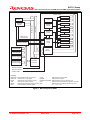
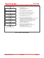
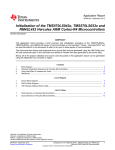
APPLICATION NOTE
SH7211 Group
Data Transfer between On-chip RAM Areas with DMAC (Cycle-Stealing Mode)
Introduction
This application note describes the operation of the DMAC, and is intended for reference to help in the design of user
software.
Target Device
SH7211
Contents
1.
Introduction ....................................................................................................................................... 2
2.
Description of Sample Application .................................................................................................... 3
3.
Documents of Reference ................................................................................................................ 11
REJ06B0732-0100/Rev.1.00
March 2008
Page 1 of 13
SH7211 Group
Data Transfer between On-chip RAM Areas with DMAC (Cycle-Stealing Mode)
1.
1.1
Introduction
Specification
• DMAC channel 0 is used.
• Auto-request mode is used as the interrupt source for activating DMA transfer.
• Cycle-stealing mode is used as the bus mode.
1.2
Used Module
• Direct memory access controller (DMAC channel 0)
1.3
Applicable Conditions
• Microcontroller:
• Operating Frequency:
• C Compiler:
SH7211
Internal clock
160 MHz
Bus clock
40 MHz
Peripheral clock 40 MHz
SuperH RISC engine family C/C++ compiler package Ver.9.01,
from Renesas Technology
REJ06B0732-0100/Rev.1.00
March 2008
Page 2 of 13
SH7211 Group
Data Transfer between On-chip RAM Areas with DMAC (Cycle-Stealing Mode)
2.
Description of Sample Application
In this sample application, the direct memory access controller (DMAC) is set to auto request mode to transfer 512Kbtyte data stored in the on-chip RAM to another address.
2.1
Operation of Modules Used
When a DMA transfer request is made, the DMAC starts to transfer data in accordance with the priority order of
channels and continues the transfer operation until the transfer end condition is met. Transfer requests for the DMAC
are of three kinds: auto requests, external requests, and on-chip peripheral module requests. The bus mode is selectable
as burst mode or cycle-stealing mode.
For details on the DMAC, refer to the section on the direct memory access controller in the SH7211 Group Hardware
Manual.
An overview of the DMAC is given in table 1. Examples of DMA transfer in cycle-stealing mode and burst mode are
shown in figures 1 and 2, respectively. In addition, a block diagram of the DMAC is shown in figure 3.
Table 1
Overview of DMAC
Item
Number of channels
Address space
Length of transfer data
Maximum transfer count
Address mode
Transfer request
Bus mode
Priority level
Interrupt request
External request detection
Transfer request acknowledge
signal/transfer end signal
REJ06B0732-0100/Rev.1.00
Description
8 (CH0 to CH7)
Only 4 (CH0 to CH3) can receive external requests.
4 Gbytes
Byte, word (2 bytes), longword (4 bytes), and 16 bytes (longword × 4)
16,777,216 (24 bits) transfers
Single address mode and dual address mode
External request, on-chip peripheral module request, and auto request
(SCIF: 8 sources, IIC3: two sources, A/D converter: one source, MTU2:
five sources, CMT: two sources)
Cycle-stealing mode (normal mode and intermittent mode) and burst
mode
Channel priority fixed mode and round-robin mode
An interrupt request to the CPU is made when half or all of a transfer
process is completed.
DREQ input low/high level detection, rising/falling edge detection
Active levels for DACK and TEND can be set independently
March 2008
Page 3 of 13
SH7211 Group
Data Transfer between On-chip RAM Areas with DMAC (Cycle-Stealing Mode)
In the normal mode of cycle stealing, bus mastership is given to another bus master after each DMA
transfer of one transfer unit (byte, word, longword, or 16-byte unit). When a subsequent transfer
request occurs, bus mastership is obtained from the other bus master and transfer proceeds for one
transfer unit. When that transfer ends, the bus mastership is passed to another bus master. This is
repeated until the transfer end condition is satisfied.
The cycle-stealing normal mode can be used in transfer across any interval, regardless of the
requesting source, source, and destination of the transfer.
DREQ
Bus mastership returned to CPU once
Bus cycle
CPU
CPU
CPU
DMAC
DMAC
Read
Write
CPU
DMAC DMAC
Read
CPU
Write
Figure 1 DMA Transfer Example in Cycle-Stealing Normal Mode
(Dual Address, DREQ Low Level Detection)
In burst mode, once the DMAC has obtained bus mastership, it continues to perform transfer without
releasing the bus until the transfer end condition is satisfied. In external mode, however, when the DREQ
signal is being level-detected and changes to the non-active level, even if the tranfer end condition has not
been satisfied, bus mastership is passed to another bus master on completion of the DMA transfer request
for which the request has already been accepted.
DREQ
Bus cycle
CPU
CPU
CPU
DMAC
DMAC
DMAC
DMAC
Read
Write
Read
Write
CPU
CPU
Figure 2 DMA Transfer Example in Burst Mode (Dual Address, DREQ Low Level Detection)
REJ06B0732-0100/Rev.1.00
March 2008
Page 4 of 13
SH7211 Group
Data Transfer between On-chip RAM Areas with DMAC (Cycle-Stealing Mode)
DMAC module
RDMATCR_n
On-chip
memory
Iteration
control
RSAR_n
Register
control
Internal bus
Peripheral bus
On-chip
peripheral
module
DMATCR_n
SAR_n
RDAR_n
Start-up
control
DAR_n
DMA transfer
request signal
CHCR_n
DMA transfer acknowledge signal
HEIn
Interrupt controller
DEIn
Request
priority
control
DMAOR
DMARS0 to DMARS3
External ROM
Bus
interface
External RAM
External device
(memory mapped)
External device
(with acknowledge)
Bus state
controller
DREQ0 to DREQ3
DACK0 to DACK3,
TEND0, TEND1
[Legend]
RDMATCR:
DMATCR:
RSAR:
SAR:
RDAR:
DAR:
DMA reload transfer count register
DMA transfer count register
DMA reload source address register
DMA source address register
DMA reload destination address register
DMA destination address register
CHCR:
DMAOR:
DMARS0 to DMARS3:
HEIn:
DEIn:
n:
DMA channel control register
DMA operation register
DMA extension resource selectors 0 to 3
DMA transfer half-end interrupt request to the CPU
DMA transfer end interrupt request to the CPU
0, 1, 2, 3, 4, 5, 6, 7
Figure 3 Block Diagram of DMAC
REJ06B0732-0100/Rev.1.00
March 2008
Page 5 of 13
SH7211 Group
Data Transfer between On-chip RAM Areas with DMAC (Cycle-Stealing Mode)
2.2
Operational Description of Sample Program
The settings of the DMAC for the sample program are listed in table 4. Also, the operation of the sample program is
illustrated in figure 4.
Table 4
Settings of DMAC
DMA transfer condition
Channel
Length of transfer data
Maximum transfer count
Address mode
Bus mode
Priority level
Interrupt request
Auto request mode
CH0
4 bytes
128 transfers (128 × data length of 4 bytes = 512-byte data)
Dual address mode
Cycle-stealing mode
Channel priority level fixed mode
Disable an interrupt request to the CPU at the end of a transfer
DMAC
Transfer source
address
On-chip RAM
H'0xFFF81000
SAR
512-byte data
DAR
DMA transfer
Transfer
destination
address
H'0xFFF82000
512-byte data
[Legend]
SAR:Source address register
DAR:Destination address register
Figure 4 Operation of Sample Program
REJ06B0732-0100/Rev.1.00
March 2008
Page 6 of 13
SH7211 Group
Data Transfer between On-chip RAM Areas with DMAC (Cycle-Stealing Mode)
2.3
Procedure for Setting Modules
This section describes the procedure for making initial settings when the DMAC is to be used to transfer data between
locations within the on-chip RAM. Auto request mode is used for the transfer requests.
By default, the on-chip peripheral modules of this MCU are in module standby mode. Whenever any of these modules
is to be used, be sure to take it out of module standby mode before making the initial settings. Although processing to
delete the end of DMA transfer is typically handled by interrupts, polling is used in this sample application. A
flowchart of the sample program is shown in figure 5. In addition, a flowchart of DMAC initialization is shown in
figure 6.
For details on registers, refer to the SH7211 Group Hardware Manual.
main
STB.CR2.BIT._DMAC = 0
[1]
[1] Cancel module standby mode
Activate the DMAC
DMAC_init
[2]
[2] Initialize the DMAC (channel 0)
512-byte Initialization
completed?
No
[3]
[3] Initialize the transfer destination
Clear a 512-byte area to 0
[4]
[4] Enable DMA transfer
Set DMA enable flag
Yes
DMAC0.CHCR.BIT.DE = 1
No
Transfer completed?
[5]
Yes
[5] Perform DMA transfer end processing
Disable DMA transfer after confirmation
of the tranfer end.
DMAC0.CHCR.BIT.DE = 0
END
* In this sample application, sleep processing is performed after the main routine is complete.
Figure 5 Flowchart of Sample Program
REJ06B0732-0100/Rev.1.00
March 2008
Page 7 of 13
SH7211 Group
Data Transfer between On-chip RAM Areas with DMAC (Cycle-Stealing Mode)
DMAC_init
Set DMA channel control register
(CHCR_0)
[1]
[2] Set the DMA transfer source address (SAR_0)
Specify the DMA transfer source address
Set DMA source address register
(SAR_0)
[2]
Set DMA destination address
register (DAR_0)
[3]
Set DMA transfer count register
(DMATCR_0)
[4]
Set DMA channel control register
(CHCR_0)
[5]
Set DMA operation register
(DMAOR)
[6]
END
[1] Disable DMA transfer
Set the DE (DMA enable) bit to 0
Disable DMA transfer
[3] Set the DMA transfer destination address (DAR_0)
Specify the DMA transfer destination address
[4] Specify the DMA transfer count (DMATCR_0)
Set the DMA transfer count to 128
[5] Set the channel control register (CHCR_0)
Set TC to B’1: transfer data for the count specified in DMATCR
Set RLD to B’0: disable the reload function
Set RS[3:0] (resource selector) to B’0100: auto request
Set DM[1:0] to B’01: increment the destination address
Set SM[1:0] to B’00: fix the source address
Set TB to B’0: cycle steal mode
Set IE to B’0: disable interrupts
[6] Set the DMA operation register (DMAOR)
Read from the AE and MNIF bits and clear them to 0
Clear the address error flag
Set the DME bit to 1 after clearing the flags
Enable DMA transfer on all the channels
Figure 6 Flowchart of Initializing DMAC
REJ06B0732-0100/Rev.1.00
March 2008
Page 8 of 13
SH7211 Group
Data Transfer between On-chip RAM Areas with DMAC (Cycle-Stealing Mode)
2.4
2.4.1
Register Settings for Sample Program
Clock Pulse Generator (CPG)
The settings of the clock pulse generator for the sample program are described in table 5.
Table 5
Settings of Clock Pulse Generator
Register Name
Frequency control
register (FRQCR)
2.4.2
Address
H’FFFE0010
Setting Value
H’1303
Description
CKOEN = “B’1”: output clocks
STC[1:0] = “B’00”: frequency multiplication
ratio of PLL circuit × 1
IFC[2:0] = “B’000”: internal clock × 1
PFC[2:0] = “B’011”: peripheral clock × 1/4
Standby Control Register
The settings of the standby control register for the sample program are described in table 6.
Table 6
Settings of Standby Control Register
Register Name
Standby control
register 2 (STBCR2)
Address
H’FFFE0018
REJ06B0732-0100/Rev.1.00
Setting Value
H’00
March 2008
Description
MSTP8 = “B’0”: the DMAC operates
Page 9 of 13
SH7211 Group
Data Transfer between On-chip RAM Areas with DMAC (Cycle-Stealing Mode)
2.4.3
Direct Memory Access Controller (DMAC)
The settings of DMAC registers for the sample program are described in table 7.
Table 7
Settings of DMAC Registers
Register Name
DMA source address
register 0 (SAR)
DMA destination address
register 0 (DAR)
DMA transfer count
register 0 (DMATCR)
Address
H’FFFE1000
Setting Value
H’FFF81000
Description
Transfer source start address
H’FFFE1004
H’FFF82000
Transfer destination start address
H’FFFE1008
D’128
DMA transfer count:
128 transfers
DMA channel control
register 0 (CHCR)
H’FFFE100C
H’0000 0000
Before DMA initialization
DE = “B’0”: disables DMA transfer
DMA initialization
TC = “B’1”: transfers data for the count
specified in DMATCR for each transfer
request
DM[1:0] = “B’01”: increments the destination
address
SM[1:0] = “B’00”: fixes the source address
RS[3:0] = “B’0100”: auto request
TB = “B’0”: cycle-stealing mode
TS[1:0] = “B’10”: longword (4 bytes) unit
IE = “B’0”: disables interrupt requests
DE = “B’0”: disables DMA transfer
When enabling DMA transfer
DE = “B’1”: enables DMA transfer
When disabling DMA transfer
DE = “B’0”: disables DMA transfer
DME = “B’1”: enables DMA transfer on all the
channels
H’8000 4410
H’8000 4411
H’8000 4410
DMA operation register
(DMAOR)
H’FFFE1200
REJ06B0732-0100/Rev.1.00
H’0000 0001
March 2008
Page 10 of 13
SH7211 Group
Data Transfer between On-chip RAM Areas with DMAC (Cycle-Stealing Mode)
3.
Documents for Reference
• Software Manual
SH-2A, SH2A-FPU Software Manual
The most up-to-date version of this document is available on the Renesas Technology Website.
• Hardware Manual
SH7211 Group Hardware Manual
The most up-to-date version of this document is available on the Renesas Technology Website.
REJ06B0732-0100/Rev.1.00
March 2008
Page 11 of 13
SH7211 Group
Data Transfer between On-chip RAM Areas with DMAC (Cycle-Stealing Mode)
Website and Support
Renesas Technology Website
http://www.renesas.com/
Inquiries
http://www.renesas.com/inquiry
[email protected]
Revision Record
Rev.
1.00
Date
Mar.21.08
Description
Page
Summary
—
First edition issued
All trademarks and registered trademarks are the property of their respective owners.
REJ06B0732-0100/Rev.1.00
March 2008
Page 12 of 13
SH7211 Group
Data Transfer between On-chip RAM Areas with DMAC (Cycle-Stealing Mode)
Notes regarding these materials
1.
2.
3.
4.
5.
6.
7.
8.
9.
10.
11.
12.
13.
This document is provided for reference purposes only so that Renesas customers may select the appropriate
Renesas products for their use. Renesas neither makes warranties or representations with respect to the
accuracy or completeness of the information contained in this document nor grants any license to any intellectual
property rights or any other rights of Renesas or any third party with respect to the information in this document.
Renesas shall have no liability for damages or infringement of any intellectual property or other rights arising out
of the use of any information in this document, including, but not limited to, product data, diagrams, charts,
programs, algorithms, and application circuit examples.
You should not use the products or the technology described in this document for the purpose of military
applications such as the development of weapons of mass destruction or for the purpose of any other military
use. When exporting the products or technology described herein, you should follow the applicable export
control laws and regulations, and procedures required by such laws and regulations.
All information included in this document such as product data, diagrams, charts, programs, algorithms, and
application circuit examples, is current as of the date this document is issued. Such information, however, is
subject to change without any prior notice. Before purchasing or using any Renesas products listed in this
document, please confirm the latest product information with a Renesas sales office. Also, please pay regular
and careful attention to additional and different information to be disclosed by Renesas such as that disclosed
through our website. (http://www.renesas.com)
Renesas has used reasonable care in compiling the information included in this document, but Renesas
assumes no liability whatsoever for any damages incurred as a result of errors or omissions in the information
included in this document.
When using or otherwise relying on the information in this document, you should evaluate the information in light
of the total system before deciding about the applicability of such information to the intended application.
Renesas makes no representations, warranties or guaranties regarding the suitability of its products for any
particular application and specifically disclaims any liability arising out of the application and use of the
information in this document or Renesas products.
With the exception of products specified by Renesas as suitable for automobile applications, Renesas products
are not designed, manufactured or tested for applications or otherwise in systems the failure or malfunction of
which may cause a direct threat to human life or create a risk of human injury or which require especially high
quality and reliability such as safety systems, or equipment or systems for transportation and traffic, healthcare,
combustion control, aerospace and aeronautics, nuclear power, or undersea communication transmission. If you
are considering the use of our products for such purposes, please contact a Renesas sales office beforehand.
Renesas shall have no liability for damages arising out of the uses set forth above.
Notwithstanding the preceding paragraph, you should not use Renesas products for the purposes listed below:
(1) artificial life support devices or systems
(2) surgical implantations
(3) healthcare intervention (e.g., excision, administration of medication, etc.)
(4) any other purposes that pose a direct threat to human life
Renesas shall have no liability for damages arising out of the uses set forth in the above and purchasers who
elect to use Renesas products in any of the foregoing applications shall indemnify and hold harmless Renesas
Technology Corp., its affiliated companies and their officers, directors, and employees against any and all
damages arising out of such applications.
You should use the products described herein within the range specified by Renesas, especially with respect to
the maximum rating, operating supply voltage range, movement power voltage range, heat radiation
characteristics, installation and other product characteristics. Renesas shall have no liability for malfunctions or
damages arising out of the use of Renesas products beyond such specified ranges.
Although Renesas endeavors to improve the quality and reliability of its products, IC products have specific
characteristics such as the occurrence of failure at a certain rate and malfunctions under certain use conditions.
Please be sure to implement safety measures to guard against the possibility of physical injury, and injury or
damage caused by fire in the event of the failure of a Renesas product, such as safety design for hardware and
software including but not limited to redundancy, fire control and malfunction prevention, appropriate treatment
for aging degradation or any other applicable measures. Among others, since the evaluation of microcomputer
software alone is very difficult, please evaluate the safety of the final products or system manufactured by you.
In case Renesas products listed in this document are detached from the products to which the Renesas products
are attached or affixed, the risk of accident such as swallowing by infants and small children is very high. You
should implement safety measures so that Renesas products may not be easily detached from your products.
Renesas shall have no liability for damages arising out of such detachment.
This document may not be reproduced or duplicated, in any form, in whole or in part, without prior written
approval from Renesas.
Please contact a Renesas sales office if you have any questions regarding the information contained in this
document, Renesas semiconductor products, or if you have any other inquiries.
© 2008. Renesas Technology Corp., All rights reserved.
REJ06B0732-0100/Rev.1.00
March 2008
Page 13 of 13