1
Application Report
SPNA163 – September 2012
Initialization of the TMS570LS043x, TMS570LS033x and
RM42L432 Hercules ARM Cortex-R4 Microcontrollers
Charles Davenport ............................................................................................................................
ABSTRACT
This application report provides a brief overview and initialization procedure of the TMS570LS043x,
TMS570LS033x, and RM42L432 series of microcontrollers in the Hercules™ family. "Hercules MCU" will
be used henceforth in this document to refer to any part in these series of microcontrollers.
The document also shows code fragments from source files that are generated using the HALCoGen tool.
All code constructs used in this document are defined in header files also generated by the same utility.
Nearly all of the project collateral and source code discussed in this application report can be generated
using the HalCoGen tool v3.02.02 or higher.
1
2
3
4
Contents
Block Diagram ............................................................................................................... 2
Standard Initialization Sequence for Hercules Microcontrollers ...................................................... 3
Using HalCoGen to Generate the Code ................................................................................ 15
References ................................................................................................................. 15
List of Figures
1
Device Block Diagram ...................................................................................................... 2
2
FMPLL Block Diagram
3
.....................................................................................................
VIM Interrupt Address Memory Map ....................................................................................
6
13
List of Tables
1
Clock Sources on Hercules Microcontrollers ............................................................................ 6
2
Clock Domains on Hercules Microcontrollers .......................................................................... 10
Hercules is a trademark of Texas Instruments.
Cortex is a trademark of ARM Limited.
ARM is a registered trademark of ARM Limited.
All other trademarks are the property of their respective owners.
SPNA163 – September 2012
Submit Documentation Feedback
Initialization of the TMS570LS043x, TMS570LS033x and RM42L432
Hercules ARM Cortex-R4 Microcontrollers
Copyright © 2012, Texas Instruments Incorporated
1
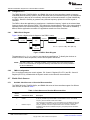
Block Diagram
1
www.ti.com
Block Diagram
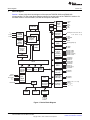
Section 1 shows a high-level block diagram of the superset TMS570LS043x and RM42L432
microcontrollers. For the actual block diagram relevant for any derivative of the TMS570LS series or for
the RM4x series of microcontrollers, see the device-specific data sheet.
DAP
AJSM
CCM-R4
FLTP1
FLTP2
Debug
Gasket
N2HET
Flash
384kB
VCCP1
with
ICEPick
128 Words
with Parity
Cortex-R4
with MPU
Cortex-R4
8 regions
with ECC
with MPU
8 regions
RAM
32kB
with ECC
SYS
GIO
GIOA[7:0]/INT[7:0]
LIN
LINRX
LINTX
LBIST
2 Regions
8 DCP
with MPU
MiBSPI1
8 Transfer
Groups
128 Buffers
with Parity
BRIDGE
OSCIN
OSCOUT
Kelvin_GND
VCCPLL
VSSPLL
16kB
CRC
R4
Flash for
EEPROM
w/ECC
2 Channel
Slave I/F
SPI2SIMO
SPI2SOMI
SPI2CLK
SPI2nCS[0]
SPI3
SPI3SIMO
SPI3SOMI
SPI3CLK
SPI3nCS[3:0]
SPI3nENA
OSC
PLL
Clock
Monitor
DCC
RTI
16 Messages
with Parity
VIM
MiBADC
96 Channel
with Parity
64 Words
with Parity
CAN1RX
CAN1TX
CAN2RX
CAN2TX
ADIN[21, 20, 17, 16, 11:0]
ADEVT
VCCAD / ADREFH
VSSAD / ADREFLO
eQEP
eQEPA
eQEPB
eQEPS
eQEPI
IOMM
32 Messages
with Parity
DCAN2
ESM
nERROR
DCAN1
PCR
MIBSPI1SIMO
MIBSPI1SOMI
MIBSPI1CLK
MIBSPI1nCS[3:0]
MIBSPI1nENA
SPI2
SCR
Peripheral
Bridge
N2HET[31:28, 26, 24:22, 20:16,
14, 12, 10, 8, 6, 4, 2, 0]
nRST
nPORRST
TEST
ECLK
STC
HTU
nTRST
TMS
TCK
RTCK
TDI
TDO
Figure 1. Device Block Diagram
2
Initialization of the TMS570LS043x, TMS570LS033x and RM42L432
Hercules ARM Cortex-R4 Microcontrollers
Copyright © 2012, Texas Instruments Incorporated
SPNA163 – September 2012
Submit Documentation Feedback
www.ti.com
2
Standard Initialization Sequence for Hercules Microcontrollers
Standard Initialization Sequence for Hercules Microcontrollers
A basic sequence for initialization and configuration of the key features on the TMS570LS043x,
TMS570LS033x, and RM42L432 microcontrollers is summarized below and many steps are detailed in the
following sections. The source code example accompanying this application report demonstrates many of
the suggested steps. Some parts of the initialization sequence are not mandatory. For example,
applications that are non-safety-critical can choose to not use the error correction coding (ECC) feature for
Flash and RAM accesses. Each application must also have its specific exception handling scheme: reset
handler, abort handler, and so forth. The code generated using the hardware abstraction layer code
generator (HALCoGen) includes template handling routines for each exception. These routines need to be
modified as required by the application.
1. Initialize the CPU registers, including stack pointers (Section 2.1).
2. Enable the Flash interface module's response to an ECC error indicated by the CPU on accesses to
Flash (Section 2.2).
3. Enable the CPU's Event Bus export mechanism (Section 2.3).
4. Enable the CPU's Single-Error-Correction Double-Error-Detection (SECDED) logic for accesses to
Flash memory (CPU's ATCM interface) (Section 2.4).
5. Handle the cause of reset to determine whether or not to continue with the start-up sequence
(Section 2.5)
6. Check if any ESM group3 error was indicated during power-up. If any ESM group3 error occurred
during the power-up, it is not safe to continue code execution and the microcontroller initialization
process can be stopped at this point. The subsequent steps in this sequence assume that there was
no ESM group3 error during power-up.
7. Configure phase-locked loop (PLL) control registers with the largest value for the last-stage of the
dividers (R-dividers) (Section 2.6).
8. Enable the PLLs (Section 2.7).
9. Run the eFuse controller start-up checks and start the self-test on the eFuse controller SECDED logic
(Section 2.8).
10. Release the peripherals from reset and enable clocks to all peripherals (Section 2.9).
11. Set up the device-level multiplexing options as well as the input/output (I/O) multiplexing.
12. Wait for the eFuse controller ECC logic self-test to complete and check the results.
13. Set up the Flash module for the required wait states and pipelined mode (Section 2.10).
14. Set up the Flash bank and pump power modes (Section 2.11).
15. Trim the LPO (Section 2.12).
16. Run the self-test on the SECDED logic embedded inside the Flash module (Section 2.13).
17. Wait for main PLL output to become valid.
18. Map the device clock domains to the desired clock sources (Section 2.14).
19. Reduce the values of the R-dividers in steps to attain the target PLL output frequency for both PLL1
and PLL2.
20. Run a diagnostic check on the CPU self-test controller (Section 2.15). A CPU reset is asserted upon
completion of the CPU self-test. Therefore, the initialization steps leading up to the reset handler will
be repeated.
21. Run the built-in self-test for the CPU (LBIST) (Section 2.16). A CPU reset is asserted upon completion
of the CPU self-test. Therefore, the initialization steps leading up to the reset handler will be repeated.
22. Run a diagnostic check on the CPU compare module (CCM-R4) (Section 2.17).
23. Run a diagnostic check on the memory self-test controller (Section 2.18).
24. Start a self-test on the CPU RAM using the programmable built-in self-test (PBIST) controller and wait
for this self-test to complete and pass (Section 2.19).
25. Initialize the CPU RAM using the system module hardware initialization mechanism so that the ECC
region for the CPU RAM is also initialized (Section 2.20).
26. Enable the CPU's SECDED logic for accesses to CPU RAM memory (CPU's B0TCM and B1TCM
interfaces) (Section 2.21).
SPNA163 – September 2012
Submit Documentation Feedback
Initialization of the TMS570LS043x, TMS570LS033x and RM42L432
Hercules ARM Cortex-R4 Microcontrollers
Copyright © 2012, Texas Instruments Incorporated
3
Standard Initialization Sequence for Hercules Microcontrollers
www.ti.com
27. Start a self-test on all on-chip dual-port SRAMs using the PBIST controller (Section 2.22).
28. Run the self-test on the CPU's SECDED logic for accesses to main data RAM (B0TCM and B1TCM)
(Section 2.23).
29. Run the self-test on the CPU's SECDED logic for accesses to the main Flash memory (ATCM)
(Section 2.24).
30. Wait for self-test to complete and pass on all on-chip dual-port SRAMs.
31. Start a self-test on all on-chip single-port SRAMs excluding the CPU RAM using the PBIST controller
(Section 2.25).
32. Wait for self-test to complete and pass on all on-chip single-port SRAMs.
33. Start auto-initialization for all other on-chip SRAMs (Section 2.26).
34. Check if the auto-initialization process for all RAMs is completed; wait here if it has not completed.
35. Check the parity error detection mechanism for all peripheral memories (Section 2.27).
36. Enable the CPU’s dedicated vectored interrupt controller (VIC) port (Section 2.28).
37. Program all interrupt service routine addresses in the vectored interrupt manager (VIM) memory
(Section 2.29).
38. Configure IRQ and FIQ interrupt priorities for all interrupt channels (Section 2.29.1).
39. Enable the desired interrupts (IRQ or FIQ) inside the CPU (Section 2.30).
40. Enable the desired interrupts in the VIM control registers (Section 2.29.2).
41. Set up the application responses to inputs to the error signaling module (ESM) (Section 2.31).
42. Initialize copy table, global variables, and constructors (Section 2.32).
43. Verify that the dual-clock-comparator (DCC) module can actually detect and flag a frequency error
(Section 2.33).
44. Configure the DCC module to continuously monitor the PLL output(Section 2.33).
45. Verify that a memory protection unit (MPU) violation for all bus masters is flagged as an error to the
ESM(Section 2.33).
46. Run a background check on entire Flash using CRC(Section 2.33).
47. Run the offset error calibration routine for the analog-to-digital converter (ADC)(Section 2.33).
48. Run a self-test on the ADC analog input channels(Section 2.33).
49. Check I/O loop-back for all peripherals(Section 2.33).
50. Set up the MPU for the bus masters(Section 2.33).
51. Set up the digital windowed watchdog (DWWD) module service window size and the module response
on a violation (reset or NMI)(Section 2.33).
52. Configure desired access permissions for peripherals using the peripheral central resource (PCR)
controller registers(Section 2.33).
53. Configure the external safety companion (for example, TI TPS6538x, for online diagnostic
operation)(Section 2.33).
54. Set up the real-time interrupt (RTI) module for generating periodic interrupts as required by the
application(Section 2.33).
55. Call the main application (Section 2.34).
2.1
Initialize Cortex™-R4 Registers
The TMS570LS043x, TMS570LS033x, and RM42L432 series of microcontrollers include dual Cortex-R4
CPUs running in a lock-step operation mode. A core compare module (CCM-R4) compares the output
signals from each R4 CPU. Any difference in the two CPUs’ outputs is flagged as a fault of a high-severity
level. The CPU internal registers are not guaranteed to power up in the same state for both the CPUs.
The CPU pushes the internal registers on to the stack on a function call, which could lead to the detection
of a core compare error. Therefore, the CPU internal core registers need to be initialized to a predefined
state before any function call is made.
4
Initialization of the TMS570LS043x, TMS570LS033x and RM42L432
Hercules ARM Cortex-R4 Microcontrollers
Copyright © 2012, Texas Instruments Incorporated
SPNA163 – September 2012
Submit Documentation Feedback
Standard Initialization Sequence for Hercules Microcontrollers
www.ti.com
The CPU’s call-return stack consists of a 4-entry circular buffer. When the CPU pre-fetch unit (PFU)
detects a taken procedure call instruction, the PFU pushes the return address onto the call-return stack.
The instructions that the PFU recognizes as procedure calls are, in both the ARM® and Thumb instruction
sets:
→ BL immediate
→ BLX immediate
→ BLX Rm
When the return stack detects a taken return instruction, the PFU issues an instruction fetch from the
location at the top of the return stack, and pops the return stack. The instructions that the PFU recognizes
as procedure returns are, in both the ARM and Thumb instruction sets:
→
→
→
→
→
→
→
2.2
LDMIA Rn{!}, {..,pc}
POP {..,pc}
LDMIB Rn{!}, {..,pc}
LDMDA Rn{!}, {..,pc}
LDMDB Rn{!}, {..,pc}
LDR pc, [sp], #4
BX Rm
Enable Response to ECC Errors in Flash Interface Module
The Flash module has a Flash Error Detection and Correction Control Register 1 (FEDACCTRL1) at
address 0xFFF87008. This register controls the ECC functionality implemented inside the Flash module,
including support for the SECDED logic inside the Cortex-R4 CPU. The bits 3–0 of this register make up
the EDACEN field. EDACEN is configured to 0x5 by default. The application must configure EDACEN to
0xA in order to enable the Flash module's support for the CPU's SECDED logic.
2.3
Enable the Cortex-R4 CPU’s Event Signaling Mechanism
The Cortex-R4 CPU has a dedicated event bus that is used to indicate that an event has occurred. This
event signaling is disabled upon reset and must be enabled. The Flash module and the RAM module
interfaces capture the ECC error events signaled by the CPU. This allows the application to further debug
the exact address, which caused the ECC error.
The CPU event signaling can be enabled by clearing the “X” bit of the performance monitoring unit’s
“Performance monitor control register, c9”.
2.4
Enable the Cortex-R4 CPU’s ECC Checking for ATCM Interface
The CPU has internal ECC logic that protects all CPU accesses to the ATCM (Flash) interface. This logic
is not used by default and must be enabled by setting the ATCMPCEN bit of the System control
coprocessor’s Auxiliary control register, c1.
2.5
Handle the Cause of Reset
Each application has different levels of tolerance for different reset conditions. A typical reset handler is
presented in the accompanying example code project, which identifies all the causes of a reset condition
on the Hercules MCUs.
SPNA163 – September 2012
Submit Documentation Feedback
Initialization of the TMS570LS043x, TMS570LS033x and RM42L432
Hercules ARM Cortex-R4 Microcontrollers
Copyright © 2012, Texas Instruments Incorporated
5
Standard Initialization Sequence for Hercules Microcontrollers
2.6
www.ti.com
Configure PLLs
The TMS570LS043x, TMS570LS033x, and RM42L432 series of microcontrollers contain a frequencymodulated phase-locked loop (FMPLL) macro that allows the input oscillator frequency to be multiplied to
a higher frequency than can be conveniently achieved with an external resonator or crystal. Additionally,
the FMPLL allows the flexibility to generate many different frequency options from a fixed crystal or
resonator.
The FMPLL allows the application to superimpose a “modulation frequency” signal on the selected base
frequency signal output from the FMPLL. This reduces the electromagnetic energy of the output signal by
spreading it across a controlled frequency range around the base frequency. This mode is disabled by
default, and the application can enable it in applications sensitive to noise emissions.
2.6.1
FMPLL Block Diagram
Figure 2 shows a high-level block diagram of the FMPLL macro.
OSCIN
/NR
INTCLK
VCOCLK
PLL
/1 to /64
/OD
post_ODCLK
/1 to /8
/NF
/R
PLLCLK
/1 to /32
fPLLCLK = (fOSCIN / NR) * NF / (OD * R)
/1 to /256
Figure 2. FMPLL Block Diagram
The parameters fOSCIN, fpost_ODCLK and fHCLK are data sheet specifications. To identify the minimum or
maximum limits on these frequencies, see the device-specific data sheet.
NOTE: The FMPLL takes (127 + 1024*NR) oscillator cycles to acquire lock to the target frequency,
hence it is recommended to configure the FMPLL(s) and enable them as soon as possible in
the device initialization.
2.6.2
FMPLL Configuration
PLL1 is configured using two control registers, PLL Control 1 Register (PLLCTL1) and PLL Control 2
Register (PLLCTL2), located within the System module on the Hercules microcontrollers.
2.7
Enable Clock Sources
2.7.1
Available Clock Sources on Hercules Microcontrollers
The TMS570LS043x, TMS570LS033x, and RM42L432 series of microcontrollers support five different
clock sources, as listed in Table 1.
Table 1. Clock Sources on Hercules Microcontrollers
Clock
Source
Number
0
1
6
Clock Source Name
Description
OSCIN
This is the primary oscillator, typically driven by an external resonator or crystal. This
is the only available input to the FMPLL and the FMPLL2 macros. The OSCIN
frequency must be between 5 MHz and 20 MHz.
FMPLL#1 output
This is the output of the FMPLL, which is generated using the OSCIN as the input
clock. The FMPLL output clock frequency must not exceed the maximum device
frequency specified in the device-specific data sheet. The FMPLL features a
modulation mode where a modulation frequency is superimposed on the FMPLL
output signal.
Initialization of the TMS570LS043x, TMS570LS033x and RM42L432 Hercules
ARM Cortex-R4 Microcontrollers
Copyright © 2012, Texas Instruments Incorporated
SPNA163 – September 2012
Submit Documentation Feedback
Standard Initialization Sequence for Hercules Microcontrollers
www.ti.com
Table 1. Clock Sources on Hercules Microcontrollers (continued)
Clock
Source
Number
2.7.2
Clock Source Name
Description
2
Not implemented
No clock signal is connected to source 2. This clock source must not be enabled or
chosen for any clock domain.
3
EXTCLKIN
External clock input. This clock source must only be enabled if there is an actual
external clock source connected to the identified device terminal for EXTCLKIN. For
more information, see the device-specific data sheet.
4
LF LPO
This is the low-frequency output of the internal reference oscillator. The LF LPO is
typically an 80 KHz signal, and is generally used for low-power mode use cases.
5
HF LPO
This is the high-frequency output of the internal reference oscillator. The HF LPO is
typically a 10 MHz signal, and is used as a reference clock for monitoring the main
oscillator.
6
Not Implemented
No clock signal is connected to source 6. This clock source must not be enabled or
chosen for any clock domain.
7
Not Implemented
No clock signal is connected to source 7. This clock source must not be enabled or
chosen for any clock domain.
Control Registers for Enabling and Disabling Clock Sources
There are five available clock sources on the TMS570LS043x, TMS570LS033x, and RM42L432 series of
microcontrollers:
• Clock sources 0, 4 and 5 are enabled, while clock sources 1 and 3 are disabled upon any system
reset.
• Clock sources 2, 6, and 7 are not implemented and must not be enabled in the application.
• Each bit of the system module Clock Source Disable Register (CSDIS) controls the clock source of the
same number: bit 0 controls clock source 0, bit 1 controls clock source 1, and so on.
• There are also dedicated Clock Source Disable Set (CSDISSET) and Clock Source Disable Clear
(CSDISCLR) registers to allow the application to avoid using read-modify-write operations.
• Setting any bit commands, the corresponding clock source to be disabled.
– The clock source can only be disabled once there is no clock domain or secondary clock source
(FMPLL) using the clock source to be disabled.
2.7.3
Example Clock Source Configuration
systemREG1->CSDISCLR =
|
|
|
|
0x00000000U
0x00000001U
0x00000002U
0x00000010U
0x00000020U;
//
//
//
//
Enable
Enable
Enable
Enable
clock
clock
clock
clock
source
source
source
source
0
1
4
5
The above configuration enables clock sources 0, 1, 4, and 5.
Of the clock sources that are enabled, numbers 0, 4 and 5 are enabled by default and will have become
valid by the time the processor is released from reset upon a power-up. These are the main oscillator and
the two outputs from the internal reference oscillator.
Clock source 1 is the PLL output. The FMPLL has a defined start-up time, and its output is not available
for use until this time. The application must wait for the valid status flag for this clock source to be set
before using the FMPLL output for any clock domain. The example initialization sequence makes use of
this FMPLL lock time to perform all initialization actions that don't have to be done at the maximum
operating frequency chosen for the application.
SPNA163 – September 2012
Submit Documentation Feedback
Initialization of the TMS570LS043x, TMS570LS033x and RM42L432
Hercules ARM Cortex-R4 Microcontrollers
Copyright © 2012, Texas Instruments Incorporated
7
Standard Initialization Sequence for Hercules Microcontrollers
2.8
www.ti.com
Run Self-Test on the eFuse Controller SECDED Logic
Electrically programmable fuses (eFuses) are used to configure the part after de-assertion of power-on
reset (nPORRST). The eFuse values are read and loaded into internal registers as part of the power-onreset sequence. This is called the eFuse autoload. The eFuse values are protected with single-bit errorcorrection, double-bit error-detection (SECDED) codes. These fuses are programmed during the initial
factory test of the device. The eFuse controller is designed so that the state of the eFuses cannot be
changed once the device is packaged.
For safety critical systems, it is important for the application to check the status of the eFuse controller
after a device reset. For more details on eFuse controller errors and the application sequence to check for
these errors, see the eFuse Controller chapter of the device-specific technical reference manual.
2.9
Release Reset and Clocks to Peripherals
The peripherals are kept under reset, and need to be explicitly brought out of reset by the application. This
can be done by setting the peripheral enable (PENA) bit of the Clock Control Register (CLKCNTL).
The clocks to the peripheral modules are also disabled upon any system reset and need to be explicitly
enabled by the application. This can be done by setting the bits corresponding to the peripheral select
quadrant occupied by the peripheral module in the Peripheral Central Resource (PCR) Control Registers
for clearing the power down states of peripheral modules (Peripheral Power-Down Clear Register [0:3]
(PSPWRDWNCLRx)). For information on the peripheral select quadrants for each peripheral, see the
device-specific data sheet.
2.10 Configure Flash Access
The Flash memory on the TMS570LS043x, TMS570LS033x, and RM42L432 series of microcontrollers is
a non-volatile electrically erasable and programmable memory.
The TMS570LS043x, TMS570LS033x, and RM42L432 series of microcontrollers contain a digital module
that manages all accesses to the Flash memory. A Flash access can be completed without any wait states
required for bus master clock speeds up to 45 MHz. If the bus clock is faster than 45 MHz, then any Flash
access requires the appropriate number of wait states depending on the bus clock speed. The
TMS570LS043x, TMS570LS033x, and RM42L432 series of microcontrollers support clock speeds up to
80 MHz for the TMS570LSxx3x devices and up to 100MHz for the RM42L432 device. For the actual
maximum allowed speed and the number of corresponding address and data wait states, see the devicespecific data sheet.
Suppose that the application requires a CPU clock speed of 80 MHz. This requires 1 data wait state and
no address wait states for any access to the Flash memory. These wait states need to be configured in
the Flash module registers.
The Flash module also features a pipelined mode of operation. When this mode is enabled, the module
reads 128 bits from the Flash memory and holds them in buffers that the CPU can read from without any
wait state. The CPU can read 32 or 64 bits of instructions or data from the pipeline buffers.
The Flash Read Control Register (FRDCNTL) inside the Flash module controls the wait states and the
pipeline mode.
The TMS570LS043x, TMS570LS033x, and RM42L432 series of MCUs also have a separate Flash bank
(bank number 7) that is dedicated for data storage. This bank has a different architecture that is intended
specifically to be used to emulate an EEPROM with software. Accesses to this Flash bank is configured
via a separate EEPROM Emulation Configuration Register (EEPROM_CONFIG) in the Flash module. A
write operation to the EEPROM_CONFIG register must first be enabled by configuring the Flash State
Machine Write Enable Control Register (FSM_WR_ENA).
Once the access to the FSM control registers is enabled, the read access to the Flash bank 7 can be
configured to accommodate the bank number 7 specific wait states for the selected device operating
frequencies. Reference the device specific datasheet for the appropriate number of wait states needed for
bank 7 accesses.
8
Initialization of the TMS570LS043x, TMS570LS033x and RM42L432
Hercules ARM Cortex-R4 Microcontrollers
Copyright © 2012, Texas Instruments Incorporated
SPNA163 – September 2012
Submit Documentation Feedback
Standard Initialization Sequence for Hercules Microcontrollers
www.ti.com
2.11 Configure Flash Bank and Pump Power Modes
The Flash banks and pump used on the TMS570LS043x, TMS570LS033x, and RM42L432 series of
microcontrollers support three different operating modes to optimize power consumption.
• Active mode
– Flash bank sense amplifiers and sense reference are enabled
– All circuits of Flash charge pump are enabled
• Standby mode (only for Flash banks)
– Flash bank sense reference is enabled but sense amplifiers are disabled
• Sleep Mode
– Flash bank sense amplifiers and sense reference are disabled
– All circuits of Flash charge pump are disabled
The Flash banks and charge pump are in the active state by default and after any system reset. The Flash
module allows the application to configure “fall back” power states for the Flash banks and charge pump.
The Flash banks and pump automatically switch the power mode to the selected fall back state when
there is no access to the Flash banks detected within a user-configurable time.
The Flash module also contains special timers to automatically sequence the Flash banks and pump
between the active and the selected fall-back states. A read access to any Flash bank that is in a nonactive power state “wakes up” both the selected bank and the charge pump to active power state.
Programming and erase operations are only allowed on banks in active state.
The Flash Bank Access Control Register (FBAC) controls the Flash banks’ power states.
The Flash Pump Access Control Registers (FPAC1, FPAC2) control the Flash pump's power states.
2.12 Configure Oscillator Monitor
The HF LPO clock source is used as a reference clock for monitoring the main oscillator. A failure is
detected if the oscillator frequency falls outside the range: {fHFLPO / 4, fHFLPO*4}.
The HF LPO frequency varies significantly over process corners as well as with changes in the core
supply (VCC) and temperature. The Hercules microcontrollers allow the application to trim the HF LPO
such that the application can choose the operating frequency point of the HF LPO. This in turn determines
the valid range of oscillator frequency.
During device test, a trim value is written into the one-time programmable (OTP) section of the Flash
memory, address 0xF008_01B4. Bits 31:16 of this OTP word contain a 16-bit value that may be
programmed into Low Power Oscillator Monitor Control Register (LPOMONCTL) in order to initialize the
trim for HF LPO.
Alternatively, the application can use the dual-clock compare (DCC) module to determine the trim setting
for the HF LPO. The DCC module allows for comparison of two clock frequencies. Once the HF LPO is
determined to be in-range with the initial HFTRIM setting from the OTP, the crystal oscillator may be used
as a reference against which the HF LPO and LF LPO may be further adjusted. For more details, see the
device-specific technical reference manual.
2.13 Run Self-Test on the Flash Module SECDED Logic
The Flash module reads the “reset configuration vector” from address 0xF0080140 in the TI OTP region of
Flash bank 0. This is a 64-bit value that is used to configure the device characteristics at start up. The
Flash module has built-in SECDED logic to correct any single-bit error in this vector or detect and flag any
double-bit error in this vector. If a double-bit error is detected during this read from the OTP, an ESM
group3 error condition is flagged and the nERROR signal is asserted low. If a single-bit error is detected
during the read from the OTP, this error is corrected by the SECDED logic – no flag is set and no error
signal is sent to the ESM.
SPNA163 – September 2012
Submit Documentation Feedback
Initialization of the TMS570LS043x, TMS570LS033x and RM42L432
Hercules ARM Cortex-R4 Microcontrollers
Copyright © 2012, Texas Instruments Incorporated
9
Standard Initialization Sequence for Hercules Microcontrollers
www.ti.com
There are dedicated locations within the TI OTP sector of Flash bank 0 that are programmed to have
single-bit and double-bit errors. Specifically, a 32-bit or 64-bit read from the address 0xF00803F0 results
in a single-bit error indication, and a 32-bit or 64-bit read from the address 0xF00803F8 results in a
double-bit error indication. These locations can be read by the application to ensure that the Flash
interface module is capable of detecting single-bit and double-bit errors upon reads from the OTP.
2.14 Clock Domains
All further initialization steps are now required to be performed at the max operating frequency for the
application. The application must now wait for the PLL to lock to its target frequency, and then map the
device clock domains to the desired clock sources. There are multiple clock domains on the
TMS570LS043x, TMS570LS033x, and RM42L432 series of microcontrollers to ease the configuration and
controllability of the different modules using these clock domains (see Table 2).
Table 2. Clock Domains on Hercules Microcontrollers
Domain Name
Clock Name
Comments
CPU clock domain
GCLK
GCLK controls all the CPU sub-systems, including the floating point
unit (FPU), and the memory protection unit (MPU)
System bus clock domain
HCLK
HCLK shares the same clock source as GCLK, and is always the
same frequency as HCLK.
System peripheral clock domain
VCLK_sys
VCLK_sys is used for the system modules such as VIM, ESM, SYS,
and so forth. VCLK_sys is divided down from HCLK by a
programmable divider from 1 to 16.
VCLK, VCLK2
VCLK is the primary peripheral clock, and is synchronous with
VCLK_sys. VCLK2 is a secondary peripheral clock and is reserved
for use by the enhanced timer module (N2HET) and the associated
transfer unit (HTU). VCLK2 is also divided down from HCLK by a
programmable divider from 1 to 16. fHCLK must be an integer multiple
of fVCLK2, fVCLK2 must be an integer multiple of fVCLK. NOTE: The clock
domain used for eQEP is VCLK; however, in order to provide an
extra level of control to the clocking of eQEP, VCLK clocking to
eQEP may be disabled separately from the VCLK domain
through CDDIS bit 9.
Asynchronous clock domain
VCLKA1
This clock domain is reserved for use by special communication
modules that have strict jitter constraints. For the TMS570LS043x,
TMS570LS033x, and RM42L432 series of microcontrollers this is
limited to the DCAN modules. The protocol for DCAN
communication does not allow modulated clocks to be used for the
baud rate generation. The asynchronous clocks allow the clock
sources for the baud clocks to be decoupled from the GCLK, HCLK
and VCLKx clock domains.
Real-time Interrupt clock domains
RTI1CLK
This clock is used for generating the periodic interrupts by the RTI
module.
Peripheral clock domains
2.14.1
Mapping Clock Domains to Clock Sources
The system module on the TMS570LS043x, TMS570LS033x, and RM42L432 series of microcontrollers
contains registers that allow the clock domains to be mapped to any of the available clock sources.
The clock source for the GCLK, HCLK , and VCLKx domains is selected by the GCLK, HCLK, VCLK, and
VCLK2 Source Register (GHVSRC).
The clock sources for the VCLKA1 domain is selected via the Peripheral Asynchronous Clock Source
Register (VCLKASRC).
The clock source for the RTI1CLK domain is selected via the RTI Clock Source Register (RCLKSRC).
10
Initialization of the TMS570LS043x, TMS570LS033x and RM42L432
Hercules ARM Cortex-R4 Microcontrollers
Copyright © 2012, Texas Instruments Incorporated
SPNA163 – September 2012
Submit Documentation Feedback
Standard Initialization Sequence for Hercules Microcontrollers
www.ti.com
2.14.2
Example Clock Domain Mapping
systemREG1->GHVSRC
=
|
|
systemREG1->VCLKASRC =
systemREG1->RCLKSRC =
|
2.14.3
(0U << 24U)
(0U << 16U);
(1U);
(0U);
(1U << 8U)
(0U);
//
//
//
//
//
//
Use
Use
Use
Use
Set
Use
main oscillator as wake up source for GHV CLK
main oscillator for HV CLK when GCLK is off
FMPLL as current source for GHV CLK
main oscillator for DCANx bit timings
the RTI1CLK divider to divide-by-2
FMPLL as source for RTI1CLK
Configuring VCLK , VCLK2 Frequencies
The VCLK and VCLK2 clock signals are divided down from the HCLK clock signal. These are independent
dividers that can be configured via the system module clock control register (CLKCNTL).
NOTE:
•
•
VCLK2 frequency must also be an integer multiple of VCLK frequency.
There must be some delay between configuring the divide ratios for VCLK2 and VCLK.
2.15 Run a Diagnostic Check on CPU Self-Test Controller (STC)
This involves running one CPU self-test interval in STC check mode. The STC self-check mode causes a
stuck-at-0 fault to be introduced inside one of the two CPUs for there to be an STC failure. If no STC
failure is indicated, this would mean that the STC is not capable of detecting a fault inside the CPU, and
device operation is not reliable. For information on the configuration and execution of the STC self-test,
see the device-specific technical reference manual. The CPU will be reset once the STC self-test is
completed. The reset handler routine can resume the device initialization from the next step in the
sequence.
2.16 Run CPU Self-Test (LBIST)
For information on the configuration and execution of the CPU self-test, see the device-specific technical
reference manual. The CPU will be reset once the self-test is completed. The reset handler routine can
resume the device initialization from the next step in the sequence.
2.17 Run a Diagnostic Check on the CPU Compare Module (CCM-R4)
The CCM-R4 compares the dual Cortex-R4 CPU outputs on each CPU clock cycle. Any mismatch is
indicated as an ESM group2 error. This ensures that the two CPUs are indeed operating in a lock-step
mode. The CCM-R4 module also allows the application to test the different error conditions using built-in
self-test routines. For information on how to configure the CCM-R4 in a self-test mode, see the devicespecific technical reference manual.
2.18 Run a Diagnostic Check on the Programmable Built-In Self-Test (PBIST) Controller
The PBIST engine is used to run memory test routines on all on-chip memories. It is critical for the
application to rely on this engine being able to detect and report a memory fault condition. Therefore, it is
necessary for the application to test this error detection and reporting mechanism before actually using it
to test the on-chip memories. This is done by choosing to run a RAM test routine on a ROM memory. This
test must generate a memory test failure. The application can look for the error flag to ensure that the
PBIST controller can indeed detect and report a memory test failure. For information on how to configure
the PBIST controller for executing specific memory test algorithms on selected on-chip memories, see the
device-specific technical reference manual .
2.19 Start a Self-Test on the CPU RAM Using the PBIST Controller
The CPU RAM is tested first, so that the application can continue to execute while other memories are
being tested later. For information on configuring the PBIST controller, see the device-specific technical
reference manual.
SPNA163 – September 2012
Submit Documentation Feedback
Initialization of the TMS570LS043x, TMS570LS033x and RM42L432
Hercules ARM Cortex-R4 Microcontrollers
Copyright © 2012, Texas Instruments Incorporated
11
Standard Initialization Sequence for Hercules Microcontrollers
www.ti.com
2.20 Initialize the CPU RAM
The system module hardware for auto-initialization of on-chip memories also initializes the associated
ECC or parity locations. This mechanism is now used to initialize the CPU RAM. This process clears the
CPU RAM to all zeros and also programs the corresponding ECC locations.
2.21 Enable the Cortex-R4 CPU’s ECC Checking for BxTCM Interface
The CPU has internal ECC logic that protects all CPU accesses to the BTCM (RAM) interfaces. This logic
is not used by default and must be enabled by setting the B1TCMPCEN and B0TCMPCEN bits of the
System control coprocessor’s Auxiliary control register, c1.
2.22 Start a Self-Test on All Dual-Port Memories’ Using the PBIST Controller
Separate algorithms are used for testing single-port versus dual-port on-chip SRAMs. For information on
executing the self-test on the on-chip memories using the programmable BIST (PBIST) engine, see the
device-specific technical reference manual.
2.23 Run a Self-Test on CPU's ECC Logic for Accesses to TCRAM
The CPU TCRAM was initialized earlier, so that all TCRAM is cleared to zeros and the corresponding
correct ECC locations are programmed. The test of the CPU's ECC logic for accesses to TCRAM involves
corrupting the ECC locations to create single-bit and two-bit ECC errors. For the sequence to test the
CPU's ECC logic for accesses to TCRAM, see the device-specific technical reference manual or the
initialization example project. Note that reading from a TCRAM location with a double-bit ECC error
causes the CPU to take a data abort exception. The initialization example project also includes an
example data abort handler.
2.24 Run a Self-Test on CPU's ECC Logic for Accesses to Program Flash
The Flash interface module supports a diagnostic mode (mode 7) that allows the application to test the
CPU's ECC logic for accesses to program Flash. For the sequence to test the CPU's ECC logic for
accesses to program Flash, see the device-specific technical reference manual or the initialization
example project. Note that reading from a program Flash location with a double-bit ECC error causes the
CPU to take a data abort exception. The initialization example project also includes an example data abort
handler.
2.25 Start a Self-Test on All Single-Port Memories’ Using the PBIST Controller
The CPU RAM can be excluded from this testing as it has already been verified before. For information on
executing the self-test on the on-chip memories using the programmable BIST (PBIST) engine, see the
device-specific technical reference manual.
2.26 On-Chip SRAM Auto-Initialization
The system module on the Hercules microcontroller allows all on-chip SRAMs to be initialized in hardware.
This is especially essential since all the on-chip memories support some form of error detection. The CPU
data RAM supports ECC while the peripheral memories support parity error detection. The autoinitialization mechanism also initializes the ECC or parity memories, as required.
2.27 Run a Self-Test on All Peripheral RAMs' Parity Protection Mechanism
Accesses to peripheral RAMs on this series of microcontroller are protected by parity error detection. Each
of the peripherals with the parity error detection for its associated memory also includes a self-test mode
to ensure that it is indeed capable of detecting and reporting a parity error on an access to the peripheral
RAM. These self-test mechanisms can be used by the application before enabling use of the concerned
peripheral.
12
Initialization of the TMS570LS043x, TMS570LS033x and RM42L432
Hercules ARM Cortex-R4 Microcontrollers
Copyright © 2012, Texas Instruments Incorporated
SPNA163 – September 2012
Submit Documentation Feedback
Standard Initialization Sequence for Hercules Microcontrollers
www.ti.com
2.28 Enable the Cortex-R4 CPU’s Vectored Interrupt Controller (VIC) Port
The CPU has a dedicated port that enables the VIM module to supply the address of an interrupt service
routine along with the interrupt (IRQ) signal. This provides faster entry into the interrupt service routine
versus the CPU having to decode the pending interrupts and identify the highest priority interrupt to be
serviced first.
The VIC port is disabled upon any CPU reset and must be enabled by the application. The VIC is enabled
by setting the VE bit in the CPU’s System Control Register (SYS).
2.29 Vectored Interrupt Manager (VIM) Configuration
The VIM module on the TMS570LS043x, TMS570LS033x, and RM42L432 series of microcontrollers
supports flexible mapping of interrupt request channels and the interrupt generating sources. The default
mapping between the channel number and the interrupting module is defined in the device-specific data
sheet. The interrupt channel number also defines the inherent priority between the channels, with the
lower numbered channel having the higher priority. That is, the priority decreases in the following order:
channel 0 → channel 1 → channel 2 → … channel 95.
For this application report, assume that the application prefers to keep the default priority order between
the channels. For details on the control registers for changing the mapping between interrupt channels
and sources, see the device-specific technical reference manual.
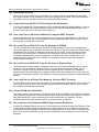
The VIM module contains a memory that holds the starting addresses of the interrupt service routines for
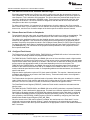
each interrupt enabled in the application. This memory starts at base address 0xFFF82000 on the
TMS570LS043x, TMS570LS033x, and RM42L432 series of microcontrollers. It is organized in 96 words of
32 bits. The VIM address memory map is shown in Figure 3.
Interrupt vector table address space
0xFFF82000
Phantom Vector
0xFFF82004
Channel 0 Vector
0xFFF82008
Channel 1 Vector
0xFFF82178
Channel 93 Vector
0xFFF8217C
Channel 94 Vector
Figure 3. VIM Interrupt Address Memory Map
2.29.1
Configure Interrupts to be Fast Interrupts or Normal Interrupts
Each interrupt request to the VIM can be configured to be forwarded to the CPU as a fast interrupt request
(FIQ) or a normal interrupt request (IRQ). The FIQ and IRQ Program Control Registers (FIRQPRx) allow
this selection.
Interrupt requests 0 and 1 are always FIQ. All others are IRQ interrupts by default.
NOTE: An interrupt request mapped to FIQ cannot use the CPU’s VIC port.
SPNA163 – September 2012
Submit Documentation Feedback
Initialization of the TMS570LS043x, TMS570LS033x and RM42L432
Hercules ARM Cortex-R4 Microcontrollers
Copyright © 2012, Texas Instruments Incorporated
13
Standard Initialization Sequence for Hercules Microcontrollers
2.29.2
www.ti.com
Enabling and Disabling Interrupts
Each interrupt request can be enabled or disabled using the Interrupt Enable Set (REQENASETx) and
Interrupt Enable Clear (REQENACLRx) registers. The interrupt requests 0 and 1 are always enabled and
cannot be disabled. When an interrupt is disabled, it does not prevent the interrupt flag from getting set
when the interrupt condition is generated but no IRQ or FIQ exception is generated for the Cortex-R4
CPU.
2.30 Enable Interrupts in the Cortex-R4 CPU
Interrupts (IRQ and FIQ) are disabled inside the Cortex-R4 CPU by default and after a CPU reset. The
normal interrupt can be enabled by clearing the "I" bit of the Current Program Status Register (CPSR)
inside the Cortex-R4 CPU, while the fast interrupt (FIQ) can be enabled by clearing the "F" bit of the
CPSR.
2.31 Setup the Error Signaling Module (ESM) Responses to Group1 Errors
The ESM allows the application to choose the module response to errors in the Group1 classification.
These are errors of the lowest severity and can be handled by the application by generating an interrupt to
the CPU. The ESM also offers the capability to indicate any group1 errors on the external nERROR pin.
2.32 Additional Initializations Required by Compiler
If the source program is written using C or C++, the TI compiler requires the creation of the C and C++
run-time environment. This includes:
• Initialization of copy table, if required
• Initialization of global and static variables defined in C and C++
• Initialization of global constructors
• Make a function call to branch to the main application
These requirements could be different for each compiler. The compiler reference manual must be referred
to identify the specific requirements for the compiler being used.
2.33 Other Initialization Steps Not Described in this Document
The following is an additional list of operations that an application can perform during the device
initialization.
• Verify that the DCC module can detect and report a frequency mismatch error.
• Configure the DCC module to continuously monitor the PLL output frequency.
• Several bus masters on the TMS570LS043x, TMS570LS033x, and RM42L432 series of microcontroller
include their own memory protection units to protect against accesses to certain parts of the memory
map. It is recommended to ensure that violations of these MPU restrictions are detected and flagged
as ESM errors.
• Configure the MPU for each bus masters
• Run a check on the program Flash memory using CRC.
• Calibrate the embedded ADC module for any offset error.
• Run a self-test on all ADC inputs to ensure that they are not open or shorted to power or ground.
• Run an I/O loop-back check on all peripheral signals.
• Configure the windowed watchdog module service window size as well as the module response to a
window violation.
• Setup the RTI module to generate periodic interrupts as necessary.
• Configure desired access permissions for peripherals using the PCR registers.
• Configure any external safety companion chip, (for example, TI TPS6538x, for online diagnostic
operation).
14
Initialization of the TMS570LS043x, TMS570LS033x and RM42L432
Hercules ARM Cortex-R4 Microcontrollers
Copyright © 2012, Texas Instruments Incorporated
SPNA163 – September 2012
Submit Documentation Feedback
Using HalCoGen to Generate the Code
www.ti.com
2.34 Call the Main Application
This is a normal function call when using C and C++. It could be a branch or branch-link to the name of
the routine that executes the application.
For example:
main();
exit();
3
Using HalCoGen to Generate the Code
Although it is not the intent of this document to serve as a guide to using HalCoGen, below are the
minimum steps necessary to generate the initialization code described in this document.
• After opening HalCoGen, select File --> New --> Project
• Select the device family (TMS570LS04x or RM42x) from the list on the left and the specific device from
the list on the right.
• Enter the desired project name and storage location and select OK. The project is now created.
• After creating the project, select the Driver Enable tab and uncheck the Mark/Un-mark all drivers check
box if it you do not want to generate all of the basic peripheral drivers. Specific drivers can be selected
at this time or none at all if you only want the initialization code.
• Once the driver selections are made, select the SAFETY INIT tab to select which of the safety
initialization routines to be included. To follow all of the suggested initializations described in this
document, select all of the available self test code to be generated.
• If drivers are to be included in the code generation, be sure to setup each of the available driver tabs
to insure the drivers are set up as needed by the specific application. Note that this should include the
necessary configuration of the IOMM module since, by default, all IOMM options are selected which
creates conflicts in the IOMM initialization. Conflicting information in the IOMM pin configuration, will
result in the default pin being active.
• Once HalCoGen is configured for you application, save the project by selecting File--> Save Project
and, finally, generate the code by selecting File-->Generate Code or pressing F5. The code generated
will be seen in a panel to the right. Files may be opened, viewed and edited within HalCoGen but there
is no build capability within HalCoGen.
• After the code is generated, a project can be created within your IDE to edit and build the code as
needed for your project.
4
References
•
•
•
•
•
TMS570LS0432/0332 16/32-Bit RISC Flash Microcontroller Data Sheet (SPNS186)
RM42L432 16/32-Bit RISC Flash Microcontroller Data Sheet (SPNS180)
TMS570LS04x/03x 16/32-Bit RISC Flash Microcontroller Technical Reference Manual (SPNU517)
RM42L432 16/32-Bit RISC Flash Microcontroller Technical Reference Manual (SPNU516)
HALCOGEN: HAL Code Generator Tool (http://www.ti.com/tool/halcogen)
SPNA163 – September 2012
Submit Documentation Feedback
Initialization of the TMS570LS043x, TMS570LS033x and RM42L432
Hercules ARM Cortex-R4 Microcontrollers
Copyright © 2012, Texas Instruments Incorporated
15
IMPORTANT NOTICE
Texas Instruments Incorporated and its subsidiaries (TI) reserve the right to make corrections, enhancements, improvements and other
changes to its semiconductor products and services per JESD46, latest issue, and to discontinue any product or service per JESD48, latest
issue. Buyers should obtain the latest relevant information before placing orders and should verify that such information is current and
complete. All semiconductor products (also referred to herein as “components”) are sold subject to TI’s terms and conditions of sale
supplied at the time of order acknowledgment.
TI warrants performance of its components to the specifications applicable at the time of sale, in accordance with the warranty in TI’s terms
and conditions of sale of semiconductor products. Testing and other quality control techniques are used to the extent TI deems necessary
to support this warranty. Except where mandated by applicable law, testing of all parameters of each component is not necessarily
performed.
TI assumes no liability for applications assistance or the design of Buyers’ products. Buyers are responsible for their products and
applications using TI components. To minimize the risks associated with Buyers’ products and applications, Buyers should provide
adequate design and operating safeguards.
TI does not warrant or represent that any license, either express or implied, is granted under any patent right, copyright, mask work right, or
other intellectual property right relating to any combination, machine, or process in which TI components or services are used. Information
published by TI regarding third-party products or services does not constitute a license to use such products or services or a warranty or
endorsement thereof. Use of such information may require a license from a third party under the patents or other intellectual property of the
third party, or a license from TI under the patents or other intellectual property of TI.
Reproduction of significant portions of TI information in TI data books or data sheets is permissible only if reproduction is without alteration
and is accompanied by all associated warranties, conditions, limitations, and notices. TI is not responsible or liable for such altered
documentation. Information of third parties may be subject to additional restrictions.
Resale of TI components or services with statements different from or beyond the parameters stated by TI for that component or service
voids all express and any implied warranties for the associated TI component or service and is an unfair and deceptive business practice.
TI is not responsible or liable for any such statements.
Buyer acknowledges and agrees that it is solely responsible for compliance with all legal, regulatory and safety-related requirements
concerning its products, and any use of TI components in its applications, notwithstanding any applications-related information or support
that may be provided by TI. Buyer represents and agrees that it has all the necessary expertise to create and implement safeguards which
anticipate dangerous consequences of failures, monitor failures and their consequences, lessen the likelihood of failures that might cause
harm and take appropriate remedial actions. Buyer will fully indemnify TI and its representatives against any damages arising out of the use
of any TI components in safety-critical applications.
In some cases, TI components may be promoted specifically to facilitate safety-related applications. With such components, TI’s goal is to
help enable customers to design and create their own end-product solutions that meet applicable functional safety standards and
requirements. Nonetheless, such components are subject to these terms.
No TI components are authorized for use in FDA Class III (or similar life-critical medical equipment) unless authorized officers of the parties
have executed a special agreement specifically governing such use.
Only those TI components which TI has specifically designated as military grade or “enhanced plastic” are designed and intended for use in
military/aerospace applications or environments. Buyer acknowledges and agrees that any military or aerospace use of TI components
which have not been so designated is solely at the Buyer's risk, and that Buyer is solely responsible for compliance with all legal and
regulatory requirements in connection with such use.
TI has specifically designated certain components which meet ISO/TS16949 requirements, mainly for automotive use. Components which
have not been so designated are neither designed nor intended for automotive use; and TI will not be responsible for any failure of such
components to meet such requirements.
Products
Applications
Audio
www.ti.com/audio
Automotive and Transportation
www.ti.com/automotive
Amplifiers
amplifier.ti.com
Communications and Telecom
www.ti.com/communications
Data Converters
dataconverter.ti.com
Computers and Peripherals
www.ti.com/computers
DLP® Products
www.dlp.com
Consumer Electronics
www.ti.com/consumer-apps
DSP
dsp.ti.com
Energy and Lighting
www.ti.com/energy
Clocks and Timers
www.ti.com/clocks
Industrial
www.ti.com/industrial
Interface
interface.ti.com
Medical
www.ti.com/medical
Logic
logic.ti.com
Security
www.ti.com/security
Power Mgmt
power.ti.com
Space, Avionics and Defense
www.ti.com/space-avionics-defense
Microcontrollers
microcontroller.ti.com
Video and Imaging
www.ti.com/video
RFID
www.ti-rfid.com
OMAP Applications Processors
www.ti.com/omap
TI E2E Community
e2e.ti.com
Wireless Connectivity
www.ti.com/wirelessconnectivity
Mailing Address: Texas Instruments, Post Office Box 655303, Dallas, Texas 75265
Copyright © 2012, Texas Instruments Incorporated