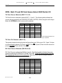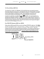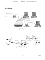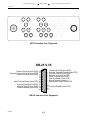
1
B
Doc #: 139001UA
Part #: 07M3040-A
DIGITAL BRIDGE
3040/V35
(CTS MD-V.35/TCB)
INSTALLATION
AND
OPERATIONS MANUAL
June 10, 1997
An ISO-9001
Certified Company
Copyright© 2000 Patton Electronics Co., All Rights Reserved
PATTON ELECTRONICS CO.
3040/V35
INSTALLATION AND OPERATIONS MANUAL
139001UA
COPYRIGHT NOTICE
Copyright© 2000 Patton Electronics Co., All Rights Reserved.
PROPRIETARY NOTICE
The information contained herein is proprietary and confidential to Patton Electronics Co. Any
reproduction or redistribution of this publication, in whole or in part, is expressly prohibited
unless written authorization is given by Patton Electronics Co.
SERVICE
All warranty and non-warranty repairs must be returned freight prepaid and insured to Patton
Electronics. All returns must have a Return Materials Authorization number on the outside of
the shipping container. This number may be obtained from Patton Electronics Technical
Services at:
tel: (301) 975-1007;
email: [email protected];
or, www: http://www.patton.com.
NOTE: Packages received without an RMA number will not be accepted.
Patton Electronics’ technical staff is also available to answer any questions that might arise
concerning the installation or use of your Patton MSDs. Technical Service hours: 8AM to 5PM
EST, Monday through Friday.
PUBLICATION NOTICE
This manual has been compiled and checked for accuracy. The information in this manual
does not constitute a warranty of performance. Patton reserves the right to revise this
publication and make changes from time to time in the content thereof. Patton assumes no
liability for losses incurred as a result of out-of-date or incorrect information contained in this
manual.
i
PATTON ELECTRONICS CO.
3040/V35
INSTALLATION AND OPERATIONS MANUAL
139001UA
EMISSION REQUIREMENTS
RADIO AND TV INTERFERENCE
The Patton devices generate and use radio frequency energy, and if not installed and used
properly—that is, in strict accordance with the manufacturer’s instructions—may cause
interference to radio and television reception. The Patton devices have been tested and found
to comply with the limits for Class A computing devices in accordance with the specifications
in Subpart J of Part 15 of FCC rules, which are designed to provide reasonable protection
from such interference in a commercial installation. However, there is no guarantee that
interference will not occur in a particular installation. If the Patton devices do cause
interference to radio or television reception, which can be determined by disconnecting the
cables, the user is encouraged to try to correct the interference by one or more of the following
measures: moving the computing equipment away from the receiver, re-orienting the receiving
antenna, and/or plugging the receiving equipment into a different AC outlet (such that the
computing equipment and receiver are on different branches).
CANADIAN EMISSIONS
This digital apparatus does not exceed the Class A limits for noise emmissions from a digital
apparatus set out in the Radio Interference Regulations of the Canadian Department of
Communications.
Le present appareil numerique n’emet pas de bruits redioelectriques depassant les limites
applicables aux appareils numeriques de la Class A prescites dans le Reglement sur le
brouillage redioelectrique edicte par le ministere des Communications du Canada.
ii
PATTON ELECTRONICS CO.
3040/V35
INSTALLATION AND OPERATIONS MANUAL
139001UA
Contents
CHAPTER 1 - OPERATION
Channel Clocking ............................................................................................................................... 1-1
Fallback Clocking ............................................................................................................................... 1-1
Channel Interface ............................................................................................................................... 1-1
Anti-streaming .................................................................................................................................... 1-2
Channel Selection Modes .................................................................................................................. 1-2
Channel Tail Circuits ......................................................................................................................... 1-3
Interface Connections ........................................................................................................................ 1-4
Front Panel LEDs .............................................................................................................................. 1-4
Channel Enable / Disable Switches .................................................................................................. 1-4
Power Supply ..................................................................................................................................... 1-4
CHAPTER 2 - SETUP AND INSTALLATION
Power Connection ............................................................................................................................. 2-1
Factory Configuration Switch Settings .............................................................................................. 2-1
Disassembly ...................................................................................................................................... 2-2
Installation .......................................................................................................................................... 2-2
Equipment Grounding (SW15-1) ....................................................................................................... 2-3
RTS To CTS Delay (SW16-1,2,3) ..................................................................................................... 2-3
Anti-Streaming (SW18-1,2,3) ............................................................................................................ 2-3
Receive Data Mode (SW18-7) .......................................................................................................... 2-3
Control Turn-Off Delay in “DATA” Switching Mode (SW15-3,4) ....................................................... 2-4
Switch on Data / Control (SW17-5,6,7,8) .......................................................................................... 2-4
Internal Baud Rates (SW15-5,6,7,8) ................................................................................................. 2-4
Fallback Clock Enable (SW16-7) ...................................................................................................... 2-5
Fallback Clocking From Sub-Channel 4 (SW16-8) ........................................................................... 2-5
Fallback Mode Selection (SW16-6) ................................................................................................... 2-5
TX Clock Source Selection (SW17-1,2,3) ......................................................................................... 2-6
TX Clock Pin Selection (SW17-4) ..................................................................................................... 2-6
RX Clock Source Selection (SW18-4,5,6) ........................................................................................ 2-6
Tail Circuit Buffers (SW16-4) ............................................................................................................ 2-7
Port DCE/DTE Selection (SW5 thru SW14) ..................................................................................... 2-7
DTR / DSR Forced Active (JP8 thru JP12) ....................................................................................... 2-8
FACTORY Test Jumpers (JP1, JP2 and JP3) .................................................................................. 2-8
APPENDIX
Typical Application .............................................................................................................. A-1
Typical Tail Circuit Configuration ......................................................................................... A-1
Interface Pins Supported ..................................................................................................... A-2
Master DTE / Sub-Channel DTE Interface Flow Diagram .................................................... A-3
Master DTE / Sub-Channel DCE Interface Flow Diagram .................................................... A-3
Master DCE / Sub-Channel DCE Interface Flow Diagram ................................................... A-4
Master DCE / Sub-Channel DTE Interface Flow Diagram .................................................... A-4
TECHNICAL SPECIFICATIONS.......................................................................................... A-5
Strapping Guide .................................................................................................................. A-6
iii
PATTON ELECTRONICS CO.
INSTALLATION AND OPERATIONS MANUAL
3040/V35
139001UA
CHAPTER 1 - OPERATION
The Patton 3040/V35 (CTS MD-V.35/TCB) is a network enhancement accessory intended for
high speed synchronous or asynchronous V.35 modem, DSU/CSU, or port sharing
applications. The 3040/V35 (CTS MD-V.35/TCB) allows for immediate expansion of a
system without the requirement of additional communication lines. The 3040/V35 (CTS MDV.35/TCB) allows any combination of up to four V.35 DCE or DTE devices to share a single
V.35 DCE or DTE high speed link in a point-to-point or multi-point polled network.
Channel Clocking
The 3040/V35 (CTS MD-V.35/TCB) is protocol transparent and operates in synchronous and
asynchronous environments at data rates up to 2.048Mbps, depending on cable length and
attached equipment. Clocking can be derived from the Master Port clock, (pins Y,AA for TT or
U,W for ETT and V,X for RT), the internal clock generator or any Sub-Channel clock, (pins
Y,AA for TT or U,W for ETT and V,X for RT).
Fallback Clocking
In the event of loss of an externally provided clock or optionally Sub-Channel 1 DCD becoming
inactive, the 3040/V35 (CTS MD-V.35/TCB) has the ability to automatically fall back to the
predetermined internal baud rate clock or the Sub-Channel 4 RX Clock (pins V,X).
Channel Interface
The 3040/V35 (CTS MD-V.35/TCB) has five V.35 (MR-34) female connectors located on the
rear of the unit. Also a DB-25 connector is provided in parallel with the Master Port V.35
connector. Each port is DCE/DTE selectable, which eliminates the need for crossover cables.
DSR or DTR can additionally be forced to the active state individually on each Sub-Channel by
Jumper control.
3040/V35
S UB-CH ANN EL STATUS
ENABLE/DISABLE
STREAM
ACTIVE
PW
SD
RD
FB
1
2
3
4
1
1-1
2
3
4
1
2
3
4
OPERATION
PATTON ELECTRONICS CO.
3040/V35
INSTALLATION AND OPERATIONS MANUAL
139001UA
Anti-streaming
A typical problem often encountered is a “STREAMING” remote terminal. The streaming
problem can tie up an entire circuit until the offending device has recovered or is powered
down. A streaming condition occurs when a Sub-Channel remains active, disrupting the
polling sequence. The 3040/V35 (CTS MD-V.35/TCB) provides two user selectable modes of
controlling a streaming condition, an automatic anti-streaming Abort Timer with eight
selectable block lengths and a setting to disable anti-streaming for large data block transfers,
and a manual Operator Control mode (front panel push button switch).
Automatic Anti-streaming - Automatic Anti-Streaming will block the asserted control signal
from the Sub-Channel Port, releasing the 3040/V35 (CTS MD-V.35/TCB) to accept requests
from any other Sub-Channel that has not been locked out due to a streaming condition. When
a Sub-Channel is locked out for streaming, a visual indication, by Sub-Channel, is provided on
the front panel. The Sub-Channel will no longer receive data or CTS from the Master Port.
Any data sent to the Master Port by the streaming device will be lost. Once a Sub-Channel is
locked out due to streaming, the Sub-Channel will remain locked out until the attached device
removes the streaming condition. If RTS is held active, RTS must become inactive, if
continuous data transitions have triggered the Anti-Stream logic, the transitions must stop
before the 3040/V35 (CTS MD-V.35/TCB) will clear the Anti-Stream logic to that Sub-Channel.
Removing the Sub-Channel via the front panel disable switch will not clear the Anti-stream
logic for a Sub-Channel once it has been activated.
Manual Anti-Streaming - If manual Anti-Stream protection is chosen, a streaming condition
caused by one of the attached terminals can be quickly corrected by the 3040/V35 (CTS MDV.35/TCB) via the associated front panel locking switches. A switch is provided for each SubChannel and permits the rapid removal of a streaming terminal without having to disconnect
any cables or power down the offending terminal. Terminals may be selectively removed for
self-test and maintenance without affecting the remaining Sub-Channels. Once the streaming
condition has been corrected, the front panel switch is simply depressed to the locked
(Enable) position (Green indicator ON) to re-establish normal operation. Removing a SubChannel with the front panel switch will block data from the Sub-Channel going to the Master
Port but will not block data going from the Master Port to the Sub-Channel as the Automatic
Anti-Stream option did.
Channel Selection Modes
The 3040/V35 (CTS MD-V.35/TCB) provides two selectable Sub-Channel service modes of
operation, the Scanning Mode and Priority Mode. Depending on system requirements, either
mode may be selected by internal DIP switch settings. Both modes switch on activity from the
Sub-Channel.
OPERATION
1-2
PATTON ELECTRONICS CO.
3040/V35
INSTALLATION AND OPERATIONS MANUAL
139001UA
In the Scanning Mode the CTS 3040/V35 (CTS MD-V.35/TCB) scans each Sub-Channel, in
sequence, beginning with Sub-Channel 1. This rotational sequence is repeated continually
with each attached Sub-Channel having equal access to the communications link. When data
or control lines from a Sub-Channel become active that Sub-Channel is switched through to
the master port by the 3040/V35 (CTS MD-V.35/TCB). All remaining Sub-Channels are
locked out until the first device becomes inactive. When the Sub-Channel device becomes
inactive, the 3040/V35 (CTS MD-V.35/TCB) will resume scanning the Sub-Channels for
another active signal.
When configured for Priority Mode operation, the 3040/V35 (CTS MD-V.35/TCB) monitors all
Sub-Channels simultaneously with Sub-Channel 1 having the highest priority. When a SubChannel becomes inactive, the 3040/V35 (CTS MD-V.35/TCB) will automatically default to the
highest priority (lowest number) Sub-Channel with activity.
Contention for the Master port is accomplished by asserting RTS (Request to Send) if the
Sub-Port is configured as a DCE, DCD (Data Carrier Detect) if the Sub-Port is configured as
a DTE or Data Transitions from the attached Sub-Channel devices in either configuration. The
active interface lead, RTS or DCD, as well as selection of contention mode, “Data Transitions”
or “Interface Lead” activation, can be selected on an individual basis for each Sub-Channel.
Once a Sub-Channel asserts an active control signal the control signal will be passed through
to the Master Port, depending on DTE / DCE configuration of the Sub-Channel and Master
Port. This control will be passed without delays. If the Master Port is configured as a DTE the
signal will be passed as RTS. The CTS returned to the Master will have an optional delay
added before the signal is returned to the Sub-Channel port.
Port Enable / Disable, front panel switches must be pushed in (GREEN indication) for a SubChannel to access the Master Port regardless of the mode of operation selected.
Channel Tail Circuits
A buffer is built into the unit for tail circuit (DCE to DCE) applications. An 8 bit centered ring
buffer is used to correct the clock phasing errors generated between the Modem on the
Master Port and the Sub-Channel port for the data transferred from the Sub-Channel to the
Master Port. If the unit is operated in an asynchronous environment the buffer must be
bypassed. This is accomplished by moving the SYNC/ASYNC switch to ASYNC.
1-3
OPERATION
PATTON ELECTRONICS CO.
3040/V35
INSTALLATION AND OPERATIONS MANUAL
139001UA
Interface Connections
All connections are made via industry standard CCITT V.35 (MR-34) female connectors
located on the rear of the unit. The Following interface leads are implemented, Chassis (A),
TD (P,S), RD (R,T), RTS (C), CTS (D), DSR (E), Sig Gnd(B), DCD (F), TT (Y,AA), RT (V,X),
DTR (H), ETT (U,W).
In addition the master port can be accessed via an DB-25 with the following pinout, Chassis
(1), TD (24,11), RD (23,22), RTS (4), CTS (5), DSR (6), Sig Gnd(7), DCD (8), TT (14,1), RT
(16,3), DTR (20), ETT (15,2).
Front Panel LEDs
Front panel LEDs are provided to indicate power is applied, RD and TD activity from the
Master Port, Sub-Channel activity of each individual Port, Anti-Stream condition of each SubChannel and an indication of clock Fallback condition.
Channel Enable / Disable Switches
Front panel switches allow operator intervention to remove an individual Sub-Channel from
accessing the Master Port. Positive latching type switches are provided for each SubChannel port for isolating or removing a streaming terminal. The Sub-Channel is activated by
IN
pushing the switch until it is in the “IN
IN” position. The switch will indicate GREEN in color. To
OUT
disable a Sub-Channel push the switch until it locks in the “OUT
OUT” position, the switch will
indicate BLACK in color. Disabling a Sub-Channel with the front panel does not prevent the
Sub-Channel from receiving data from the Master Port only from sending data to the Master
Port.
Power Supply
A linear power supply is located internally, an external 110/220VAC switch is located on the
rear of the unit. If chassis ground and signal ground need to be tied together this can also be
accomplished by switch selection. The unit is Rackmountable for 19" cabinets or optional 23"
cabinets, by using the provided Rackmount Kit. Safety approvals granted are UL and CSA as
well as emission approval for FCC Class A.
OPERATION
1-4
PATTON ELECTRONICS CO.
3040/V35
INSTALLATION AND OPERATIONS MANUAL
139001UA
Caution, Disconnect the POWER Before Removing The Cover
Vorsicht, Befor Deckung Abnehmen Mach Strom Zu.
CHAPTER 2 - SETUP AND INSTALLATION
Power Connection
220
Before connecting the 3040/V35 (CTS MD-V.35/TCB) to a AC power source the top cover
must be installed and secured with the supplied #8-32 screws. The unit is supplied with a 110/
220VAC voltage switch, turn the switch with
110 / 220VA Switch
Fuse Drawer
a coin or screw driver to the appropriate
voltage for your country. EXAMPLE: In
WARNING: FOR CONTINUED PROTECTION
110
AGAINST RISK OF FIRE, REPLACE ONLY
the United States of America; set to
WITH SAME TYPE AND RATING FUSE.
PORT 4
MASTER DTE/ DCE
110VAC. The unit is supplied with a
IEC power connector next to the
voltage select switch, plug the power
cord into the connector until it is firmly
IEC Power Connector
seated. You may now connect the
power cord into your AC outlet.
Factory Configuration Switch Settings
The 3040/V35 (CTS MD-V.35/TCB) is configured prior to shipment with the switches set to the
following default positions:
Switch 15 - 1,2,3, 4 and 8 to OFF
OFF, 5, 6 and 7 to ON
ON.
No Data Time Out = 2048 bits
Internal Baud Rate = 56000
Chassis Ground not connected to Signal Ground
Switch 16 - All to ON
ON.
CTS Delay = No Delay
Sync Mode
Contention Mode = Priority
Fallback Clock = Disabled
Fallback Clock Mode = Data Transitions
Fallback Clock Source = Internal Baud Rate Generator
Switch 17 - All to ON
ON.
TX Clock Source = Master pin 15
Sub-Channel Activity Indicated by Interface Control (RTS/DCD)
2-1
SETUP & INSTALLATION
PATTON ELECTRONICS CO.
3040/V35
INSTALLATION AND OPERATIONS MANUAL
139001UA
Switch 18 - 1, 2, 3, 7 and 8 to OFF
OFF, 4, 5 and 6 to ON
Anti-Stream timer = 2 M bits
Anti-Stream = Disabled
Broadcast Data to Sub-Channels
RX Clock Source = Master
JP4 Thru JP7 Open
HS Option Not Enabled
JP8 thru JP12 to Open
DTR / DSR Not Forced
JP1 Thru JP3 to Installed
Factory Test Jumpers
If the system application requires one or more of the default settings to be changed, it will be
necessary to remove the top cover of the enclosure to access and change the DIP switches
located on the printed circuit board.
Disassembly
Remove the top cover by removing the phillips head screws located on the left and right sides
of the 3040/V35 (CTS MD-V.35/TCB). DTE/DCE switches SW5 through SW14, baud rate
Jumpers JP4 through JP7, interface Jumpers JP8 through JP12 and configuration switches
SW15 through SW18 are located on the PCB as indicated on the strapping guide in the
Appendix of this manual. After the switch selection activity is completed, re-install the top
cover BEFORE connecting to a AC power source.
Installation
Select an appropriate location accessible to and within six feet of an AC power outlet, the
outlet must have a ground pin receptacle for product warranty. The DCE-to-DTE cabling
between each attached device and the 3040/V35 (CTS MD-V.35/TCB) should be “Straight
Through”, shielded and terminated with male connectors. Sub-Channels are marked PORT 1
through PORT 4, the Master Port is marked, MASTER DCE/DTE. If any terminal has a priority
service mode, ensure it is connected to the port connector designated “PORT 1” on the rear
panel of the 3040/V35 (CTS MD-V.35/TCB). Secure other terminals or Modems to be
serviced to the remaining “PORT” connectors. Connect the MODEM or TERMINAL to the
connector designated “MASTER DTE/DCE”.
SETUP & INSTALLATION
2-2
PATTON ELECTRONICS CO.
3040/V35
INSTALLATION AND OPERATIONS MANUAL
139001UA
Equipment Grounding (SW15-1)
Switch SW15-1 provides for grounding interconnection in those systems requiring a
connection between (Frame Ground) and (Signal Ground). Connect ONLY if required.
RTS To CTS Delay (SW16-1,2,3)
If a CTS delay is desired, set SW16-1, 2 and 3 to the required value as indicated below.
SW16-1
SW16-2
SW16-3
Time
ON
ON
ON
No Delay
OFF
ON
ON
1mS
ON
OFF
ON
2mS
OFF
OFF
ON
4mS
ON
ON
OFF
8mS
OFF
ON
OFF
16mS
ON
OFF
OFF
32mS
OFF
OFF
OFF
64mS
Anti-Streaming (SW18-1,2,3)
The maximum data block size is user selectable via switch SW18- 1, 2 and 3. As shown
below eight block sizes are provided to the user. To disable anti-streaming set SW18-8 to the
OFF position. The maximum block size is normally defined at the time of installation.
SW18-1
SW18-2
SW18-3 CLOCKS
ON
ON
ON
1024
OFF
ON
ON
2048
ON
OFF
ON
4096
OFF
OFF
ON
16 K
ON
ON
OFF
64 K
OFF
ON
OFF
256 K
ON
OFF
OFF
1 MEG
OFF
OFF
OFF
2 MEG
2-3
SETUP & INSTALLATION
PATTON ELECTRONICS CO.
3040/V35
INSTALLATION AND OPERATIONS MANUAL
139001UA
Receive Data Mode (SW18-7)
Setting switch SW18-7 to ON sets the 3040/V35 (CTS MD-V.35/TCB) into the Gated Mode.
Only the Sub-Channel that is currently active will receive the data from the master port. Setting
position 7 to OFF enables the Broadcast mode. Receive Data from the Master Port is sent to
all Sub-Channels.
Control Turn-Off Delay in “DATA” Switching Mode (SW15-3,4)
When configured to switch on DATA, switch SW15-3 and 4 set the Sub-Channel release time
in clocks. The value selected is the number of clocks at the current baud rate that must occur
without any data transitions on the Sub-Channel to indicate that Sub-Channel has completed
its transmission and the 3040/V35 (CTS MD-V.35/TCB) can resume servicing the other SubChannels. The following table should be used to set this time period.
SW15-3
SW15-4 CLOCKS
ON
ON
16
ON
OFF
64
OFF
ON
256
OFF
OFF
2048
Switch on Data / Control (SW17-5,6,7,8)
Each sub-channel is independently selectable for switch on data or switch on an active
interface control lead. Set SW17 pos 5 to OFF if sub-channel 1 switch on Data is required.
Set pos 5 to ON if switch on interface control lead is desired. Position 6 thru 8 are associated
with sub-channels 2 thru 4.
Internal Baud Rates (SW15-5,6,7,8)
Switch SW15-5, 6, 7 and 8 select the master clock rate when Internal Clock Source is selected
on TX Clock Source or RX Clock Source. In addition the Fallback clock rate is also selected
with this option. When Fallback clocking is required, the RX Clock Source and TX Clock
Source should not be set to INTERNAL. SW15-5, 6, 7 and 8 selects the clock rate of the
Fallback Clock when Internal Clock Fallback is selected. The following table shows the
available rates.
SETUP & INSTALLATION
2-4
PATTON ELECTRONICS CO.
INSTALLATION AND OPERATIONS MANUAL
3040/V35
139001UA
SW15-5
SW15-6
SW15-7
SW15-8
Rate
ON
ON
ON
ON
HS Opt.
OFF
ON
ON
ON
768K
ON
OFF
ON
ON
384K
OFF
OFF
ON
ON
192K
ON
ON
OFF
ON
128K
OFF
ON
OFF
ON
72K
ON
OFF
OFF
ON
64K
OFF
OFF
OFF
ON
57.6K
ON
ON
ON
OFF
56K
OFF
ON
ON
OFF
48K
ON
OFF
ON
OFF
38.4K
OFF
OFF
ON
OFF
28.8K
ON
ON
OFF
OFF
19.2K
OFF
ON
OFF
OFF
14.4K
ON
OFF
OFF
OFF
9.6K
OFF
OFF
OFF
OFF
4.8K
For the High Speed Option set SW15-5, 6, 7 and 8 to ON and select the desired rate by
installing JP4 for 2048K, JP5 for 1024K, JP6 for 512K or JP7 for 256K. Only one of the four
jumpers should be installed of proper operation.
Fallback Clock Enable (SW16-7)
If Clock Fallback is required when the primary clock fails, set switch SW16-7 to OFF
OFF. If
Fallback is not required set SW16-7 to ON
ON. The Fallback clock rate is selected with the
internal baud rate option. When the Fallback is activated the FBC LED will illuminate.
Fallback Clocking From Sub-Channel 4 (SW16-8)
To use the Sub-Channel 4 RX Clock as the Fallback clock set SW16-8 to OFF
OFF. To use the
Internal Baud Rate Clock as the Fallback clock set SW16-8 to ON
ON.
Fallback Mode Selection (SW16-6)
If Fallback is required, two modes are available via switch SW16-6. To Fallback when the
transitions from the primary clock source stop, set SW16-6 to ON
ON. To Fallback when DCD on
Sub-Channel 1 becomes inactive, set SW16-6 to OFF
OFF.
2-5
SETUP & INSTALLATION
PATTON ELECTRONICS CO.
3040/V35
INSTALLATION AND OPERATIONS MANUAL
139001UA
NOTE: Both TX and RX Clock Source Select MUST Be Set !!!!
TX Clock Source Selection (SW17-1,2,3)
TX Clock Source is selected by switch SW17-1, 2 and 3. The following table indicates the
source options provided by the 3040/V35 (CTS MD-V.35/TCB). When using the unit in Async
Mode, the INTERNAL clock source must be selected.
SW17-1
SW17-2
SW17-3
Source
ON
ON
ON
Master
OFF
ON
ON
Port 1
ON
OFF
ON
Port 2
OFF
OFF
ON
Port 3
ON
ON
OFF
Port 4
OFF
ON
OFF
unused
ON
OFF
OFF
unused
OFF
OFF
OFF
Internal
Internal Must Be Selected For
Async Operation
TX Clock Pin Selection (SW17-4)
The primary transmit clock can be derived from either pins Y,AA or pins U,W. If pins Y,AA are
to be the source for primary TX Clock, set SW17-4 to ON
ON. If pins U,W are to be the source for
OFF.
primary TX & RX Clock, set SW17-4 to OFF
RX Clock Source Selection (SW18-4,5,6)
RX Clock Source is selected by SW18-4, 5 and 6. The following table indicates the source
options provided by the 3040/V35 (CTS MD-V.35/TCB). If the TXC source is pins U,W, both
RXC and TXC will be sourced from pins U,W. When the unit is used in an Async network
select INTERNAL as the source of the RX Clock.
SETUP & INSTALLATION
SW18-4
SW18-5
SW18-6
Source
ON
ON
ON
Master
OFF
ON
ON
Port 1
ON
OFF
ON
Port 2
OFF
OFF
ON
Port 3
ON
ON
OFF
Port 4
OFF
ON
OFF
unused
ON
OFF
OFF
unused
OFF
OFF
OFF
Internal
2-6
PATTON ELECTRONICS CO.
3040/V35
INSTALLATION AND OPERATIONS MANUAL
139001UA
Tail Circuit Buffers (SW16-4)
The 3040/V35 (CTS MD-V.35/TCB) has a Tail Circuit Buffer that is automatically selected
when a Sub-Channel is set as a DTE. The buffer will provide clock synchronization of the data
from the Sub-Channel to the Master Port for Tail Circuit operations. The buffer is de-activated
when the Sub-Channel is configured as a DCE. When operating in an asynchronous
environment the Buffer must be bypassed. To bypass the buffer in a synchronous or
asynchronous application, set switch SW16-4 to OFF (ASYNC). For normal operation in a
synchronous environment set SW16-4 to ON (SYNC). When using a tail circuit modem with
the 3040/V35 (CTS MD-V.35/TCB), the modem connected to the Sub-Channel, should be set
to External Transmit Clocking. The modem at the remote end of the connection should be set
to RX-TX Clocking or Slaved TX Clock. This will insure the same clock is present throughout
the network and clock slippage will not occur.
Port DCE/DTE Selection (SW5 thru SW14)
Slide switches SW5 through SW14 are used to configure DTE/DCE for each port. Slide Both
switches associated with a port to the same position. Example: If connecting a modem (DCE
Device) to the PORT, then the port should be configured as a DTE interface. Slide both
switches to the DTE position toward the interface connector. If connecting a terminal (DTE) to
the Sub-Channel, the port should be configured as a DCE. Slide both switched to the DCE
position away from the interface connector. The port is always configured opposite to the
interface that is to be connected to it.
DCE
J8 thru JP12
DCE
Forced DSR/DTR
2-7
SETUP & INSTALLATION
PATTON ELECTRONICS CO.
3040/V35
INSTALLATION AND OPERATIONS MANUAL
139001UA
DTR / DSR Forced Active (JP8 thru JP12)
DTR is tied to DSR on each of the Sub-Channel ports. If the device connected does not
supply a DTR but requires DSR (DTE) or does not supply DSR but requires DTR (DCE),
installing the forced DTR/DSR jumper (JP8-JP12) for the appropriate Sub-Channel will solve
this problem. The line is forced to +8V via an 820W resistor, providing isolation to any driver
that might be on the interface.
Channel
Jumper
Channel
Jumper
Master
JP8
3
JP11
1
JP9
4
JP12
2
JP10
FACTORY Test Jumpers (JP1, JP2 and JP3)
The three test jumpers JP1, 2 and 3, must be installed for the unit to properly function. These
jumpers are used in the manufacture and test of the product prior to shipment.
SETUP & INSTALLATION
2-8
PATTON ELECTRONICS CO.
INSTALLATION AND OPERATIONS MANUAL
3040/V35
139001UA
APPENDIX
V.35
V.35
Leased
or
Dial Line
V.35 DSU/CSU
V.35
3040/V35
3040/V35
V.35 DSU/CSU
Leased
or
Dial Line
Typical Application
External
TX Clocking
TT-Y,AA
Internal
TX Clocking
Data
Data
Data
RT-V,X
Slave
TX Clocking
RT-V,X
ETT-U,W
TT-Y,AA
Data
Slave
TX Clocking
ETT-U,W
Data
ETT-U,V
TT-Y,AA
RT-V,X
Data
RT-V,X
Buffer
Terminal
Data
Typical Tail Circuit Configuration
A-1
APPENDIX
PATTON ELECTRONICS CO.
INSTALLATION AND OPERATIONS MANUAL
3040/V35
139001UA
SG
CD
B
F
L
RD(A)
RT(A)
R
V
CTS
D
J
FG
DSR
A
E
RTS
DTR
C
H
RD(B)
RT(B)
T
X
N
K
M
Z
DD
BB
TD(A)
ETT(A)
TT(A)
P
U
Y
JJ
FF
CC
TD(B)
ETT(B)
TT(B)
S
W
AA
NN
LL
HH
EE
MM
KK
M-34 Interface Pins Supported
DB-25 V.35
1
2
3
4
5
6
7
8
9
10
11
12
13
Transmit Clock(A) (from DCE) 14
External Transmit Clock(A) (from DTE) 15
Receive Clock(A) (from DCE) 16
17
18
19
Data Terminal Ready (from DTE) 20
21
Receive Data(B) (from DCE) 22
Receive Data(A) (from DCE) 23
Transmit Data(A) (from DTE) 24
25
Transmit Clock(B) (from DCE)
External Transmit Clock(B) (from DTE)
Receive Clock(B) (from DCE)
Request to Send (from DTE)
Clear To Send (from DCE)
Data Set Ready (from DCE)
Signal Ground (common)
Data Carrier Detect (from DCE)
Transmit Data(B) (from DTE)
DB-25 Interface Pins Supported
APPENDIX
A-2
PATTON ELECTRONICS CO.
3040/V35
INSTALLATION AND OPERATIONS MANUAL
139001UA
Master Port is a DTE
Channel Port is a DTE
Pins R,T RD
Pins P,S TD
Buffer
Pins P,S TD
Clk Out
Pin C RTS
Clk In
+8v
Pin D CTS
Pins R,T RD
Pin C RTS
Pin D CTS
Pin E DSR
Pin F DCD
Pin H DTR
Pins Y,AA TT
Master TX Clock
Selection Logic
Pin E DSR
Pin F DCD
Pin H DTR
Pins Y,AA TT
Pins V,X RT
Pins U,W ETT
Master RX Clock
Selection Logic
Pins V,X RT
Pins U,W ETT
Switch Control
Master DTE / Sub-Channel DTE Interface Flow Diagram
Channel Port is a DCE
Master Port is a DTE
Pins R,T RD
Pins R,T RD
Pins P,S TD
Switch Control
Pin C RTS
Pin D CTS
Pins P,S TD
Pin C RTS
Pin D CTS
Pin E DSR
Pin F DCD
Pin H DTR
Pins Y,AA TT
Master TX Clock
Selection Logic
Pin E DSR
Pin F DCD
Pin H DTR
Pins Y,AA TT
Pins V,X RT
Pins U,W ETT
Master RX Clock
Selection Logic
Pins V,X RT
Pins U,W ETT
Master DTE / Sub-Channel DCE Interface Flow Diagram
A-3
APPENDIX
PATTON ELECTRONICS CO.
3040/V35
INSTALLATION AND OPERATIONS MANUAL
139001UA
Channel Port is a DCE
Master Port is a DCE
Pins P,S TD
Pins R,T RD
Pins R,T RD
Switch Control
Pin C RTS
Pin C RTS
Pin D CTS
Pin D CTS
Pin E DSR
Pin F DCD
Pin H DTR
Pins Y,AA TT
Pins P,S TD
+8v
+8v
Master TX Clock
Selection Logic
Pins V,X RT
Pins U,W ETT
Pin E DSR
Pin F DCD
Pin H DTR
Pins Y,AA TT
Pins V,X RT
Pins U,W ETT
Master RX Clock
Selection Logic
Master DCE / Sub-Channel DCE Interface Flow Diagram
Channel Port is a DTE
Master Port is a DCE
Pins P,S TD
Pins P,S TD
Pins R,T RD
Buffer
Clk Out
Pin C RTS
Clk In
+8v
Pin D CTS
Pin E DSR
Pin F DCD
Pin H DTR
Switch Control
+8v
Pins Y,AA TT
Master TX Clock
Selection Logic
Pins V,X RT
Pins U,W ETT
Master RX Clock
Selection Logic
Pins R,T RD
Pin C RTS
Pin D CTS
Pin E DSR
Pin F DCD
Pin H DTR
Pins Y,AA TT
Pins V,X RT
Pins U,W ETT
Master DCE / Sub-Channel DTE Interface Flow Diagram
APPENDIX
A-4
PATTON ELECTRONICS CO.
3040/V35
INSTALLATION AND OPERATIONS MANUAL
139001UA
TECHNICAL SPECIFICATIONS
Applications
Sub-Channel Interface
Multiple V.35 Sync or Async DCE or DTE devices
sharing one V.35 DCE or DTE link
CCITT V.35 female connectors (MR-34)
Master Interface
Capacity
CCITT V.35 female connector (MR-34 & DB-25)
One to Four V.35 Sync or Async DTE or DCE
devices One V.35 DCE or DTE Master Channel
Data Format
Data transparent at all data rates
Front Panel
Indicators: ..... Power, Send Data, Receive Data,
Clock Fallback, Sub-Channel Active,
Sub-Channel Stream
Switches: ...... Enable/Disable each Sub-Channel
Data Rates
Power Source
Up to 2.048Mbps
Timing
Internal: ...... DIP switch selectable
Normal: ...... From Modem
External: ...... Clock provided on any Sub-Channel
100-120/200-240 Vac, 50 to 60 Hz, 0.16/0.08
A, Switch Selectable
Environmental
Anti-streaming
Operating Temp: ....... 32° to 122°F (0° to 50°C)
Relative Humidity: ..... 5 to 90% non-condensing
Altitude: .................. 0 to 10,000 feet
Automatic:Selectable timeout intervals or disable
Dimensions
Terminal Service Modes
Height: ....... 1.75 inches (4.44 cm)
Width: ....... 17.00 inches (43.18 cm)
Length: ....... 11.00 inches (18.93 cm)
Scanning Mode: ...... Channels are continuously
scanned for activity on a
sequential basis.
Priority Mode: ........ Channels are simultaniously
monitored channel one has
highest access
Weight
4.5 lbs (2.1 Kg)
A-5
APPENDIX
SW7
SW8
SW9
SW10
SW11 SW12
SW13 SW14
256Kbps
512Kbps
1024Kbps
2048Kbps
Fall
Back
Clocking
ON
Baud Rate Select - SW15
6
7
8
Rate
5
ON ON ON ON HS Option
OFF ON ON ON 768K
ON OFF ON ON 384K
OFF OFF ON ON 192K
ON ON OFF ON 128K
OFF ON. OFF ON. 72K
ON OFF OFF ON. 64K
OFF OFF OFF ON 57.6K
ON ON ON OFF 56K
OFF ON. ON OFF 48K
ON. OFF ON OFF 38.4K
OFF OFF ON OFF 28.8K
ON. ON OFF OFF 19.2K
OFF ON. OFF OFF 14.4K
ON. OFF OFF OFF 9.6K
OFF OFF OFF OFF 4.8K
OF F
ON
TX Clock Source - SW17
2
3
1
Source
ON ON ON Master
OFF ON ON Chan1
ON OFF ON Chan2
OFF OFF ON Chan3
ON ON OFF Chan4
OFF ON OFF Unused
ON OFF OFF Unused
OFF OFF OFF Internal
8 7 6 5 4 3 2 1
OF F
Anti-Stream Timer
Rx Clock Source
Rcvr Gated=ON /Broadcast=OFF
Anti-Stream Enabled=ON
ON
RX Clock Source - SW18
5
6
4
Source
ON ON ON Master
OFF ON ON Chan1
ON OFF ON Chan2
OFF OFF ON Chan3
ON ON OFF Chan4
OFF ON OFF Unused
ON OFF OFF Unused
OFF OFF OFF Internal
Anti-Stream Timer - SW18
2
3
1
Count
ON ON ON 1024
OFF ON ON 2048
ON OFF ON 4096
OFF OFF ON 16K
ON ON OFF 64K
OFF ON OFF 256K
ON OFF OFF 1M
OFF OFF OFF 2M
Port Enable(Green) / Disable(Black)
Active Anti-Stream
12 3 4
1 23 4
INSTALLATION AND OPERATIONS MANUAL
HS Option
OF F
Tx Clock Source
TXC pinsY,AA=ON / pinsU,W=OFF
Ch1 RTS=ON /Data=OFF
Ch2 RTS=ON /Data=OFF
Ch3 RTS=ON /Data=OFF
Ch4 RTS=ON /Data=OFF
JP12
Port 4
ON
CTS Delay
Sync=ON /Async=OFF
Priority=ON /Scan=OFF
FB on CLK=ON /FB on DCD=OFF
FB Disable=ON /FB Enable=OFF
Int Clk FB=ON /Ch4 FB=OFF
Port 3
Baud Rate Selection
JP11
SW18
Port 2
No Data Timeout
JP10
Port 1
Signal to Chassis Ground
Unused
JP3
JP7
JP6
JP5
JP4
JP9
SW17
8 7 6 5 4 3 2 1
8 7 6 5 4 3 2 1
OF F
JP8
SW16
3040/V35
A-6
Factory Test Jumpers
SW6
DCE
CTS Delay Timer - SW16
1
Delay
2
3
ON ON ON No Delay
OFF ON ON 1 mS
ON OFF ON 2 mS
OFF OFF ON 4 mS
ON ON OFF 8 mS
OFF ON OFF 16 mS
ON OFF OFF 32 mS
OFF OFF OFF 64 mS
RD
J6
DTE
SW15
Power SD
J5
PATTON ELECTRONICS CO.
SW5
JP1
J4
JP8 thru JP12 Installed forces DTR/DSR for the channel
V.35 on DB-25
No Data Timer - SW15
4
Count
3
ON ON 16
ON OFF 64
OFF ON 256
OFF OFF 2048
JP2
J3
8 7 6 5 4 3 2 1
PN 139010B
139001UA
APPENDIX
J2
J1
B
7622 Rickenbacker Drive
Gaithersburg, MD 20879
Sales: 301 975-1000
Support: 301 975-1007
Web Address: www.patton.com