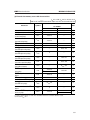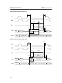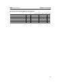
1
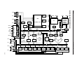
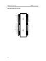
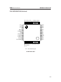
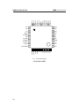
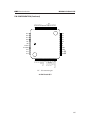
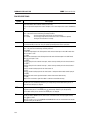
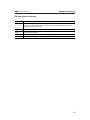
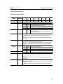
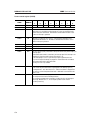
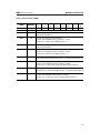
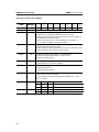
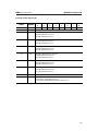
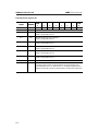
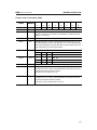
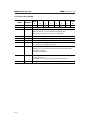
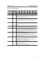
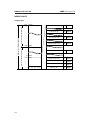
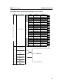
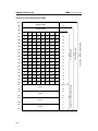
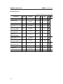
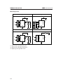
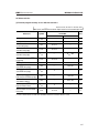
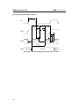
¡ Semiconductor
MSM80C154S/83C154S
¡ Semiconductor
MSM80C154S/83C154S
CMOS 8-bit Microcontroller
GENERAL DESCRIPTION
The MSM80C154S/MSM83C154S, designed for the high speed version of the existing
MSM80C154/MSM83C154, is a higher performance 8-bit microcontroller providing low-power
consumption.
The MSM80C154S/MSM83C154S covers the functions and operating range of the existing
MSM80C154/83C154/80C51F/80C31F.
The MSM80C154S is identical to the MSM83C154S except it does not contain the internal
program memory (ROM).
FEATURES
• Operating range
Operating frequency
Operating voltage
Operating temperature
: 0 to 3 MHz (Vcc=2.2 to 6.0 V)
0 to 12 MHz (Vcc=3.0 to 6.0 V)
0 to 24 MHz (Vcc=4.5 to 6.0 V)
: 2.2 to 6.0 V
: –40 to +85°C (Operation at +125°C conforms to
the other specification.)
• Fully static circuit
• Upward compatible with the MSM80C51F/80C31F
• On-chip program memory
: 16K words x 8 bits ROM (MSM83C154S only)
• On-chip data memory
: 256 words x 8 bits RAM
• External program memory address space : 64K bytes ROM (Max)
• External data memory address space
: 64K bytes RAM
• I/O ports
: 4 ports x 8 bits
(Port 1, 2, 3, impedance programmable) : 32
• 16-bit timer/counters
: 3
• Multifunctional serial port
: I/O Expansion mode
: UART mode (featuring error detection)
• 6-source 2-priority level
Interrupt and multi-level
Interrupt available by programming IP and IE registers
• Memory-mapped special function registers
• Bit addressable data memory and SFRs
• Minimum instruction cycle
: 500 ns @ 24 MHz operation
• Standby functions
: Power-down mode (oscillator stop)
Activated by software or hardware; providing
ports with floating or active status
The software power-down stet mode is terminated by interrupt signal enabling execution from
the interrupted address.
259
MSM80C154S/83C154S
• Package options
40-pin plastic DIP (DIP40-P-600-2.54)
¡ Semiconductor
:
44-pin plastic QFP (QFP44-P-910-0.80-2K) :
44-pin QFJ (QFJ44-P-S650-1.27)
:
44-pin TQFP (TQFP44-P-1010-0.80-K)
:
(Product name: MSM80C154SRS/
MSM83C154S-xxxRS)
(Product name: MSM80C154SGS-2K/
MSM83C154S-xxxGS-2K)
(Product name: MSM80C154SJS/
MSM83C154S-xxxJS)
(Product name: MSM80C154STS-K/
MSM83C154S-xxxTS-K)
xxx: indicates the code number
260
PORT 2
P0.7
PORT 0
P0.0
PCHL
XTAL1
PCH
ALE
PSEN
EA
PORT 1
PORT 3
P3.7
R/W
DPL
PLA
SP
IR
SPECIAL
FUNCTION
REGISTER
ADDRESS
DECODER
16K WORDS x 8BITS
PCL
SENSE AMP
SIGNAL
AIR
TH1
TL2
TIMER/
COUNTER 2
RCAP2L
TL1
TH0
TH2
R/W AMP
RCAP2H
RAM
256 WORDS
x 8BITS
TL0
TIMER/COUNTER 0 & 1
TMOD
ACC
TR1
TR2
RAMDP
BR
PSW
TCON
IE
INTERRUPT
ALU
IP
SBUF(T)
SBUF(R)
SERIAL IO
SCON
261
MSM80C154S/83C154S
P3.0
SIGNAL
ROM
PCON
T2CON
RESET
P1.7
CONTROL
C-ROM
IOCON
OSC and TIMING
XTAL2
P1.0
PCLL
ADDRESS DECODER
DPH
¡ Semiconductor
P2.7
BLOCK DIAGRAM (MSM83C154S)
P2.0
MSM80C154S/83C154S
¡ Semiconductor
PIN CONFIGURATION (TOP VIEW)
P1.0/T2
1
40
VCC
P1.1/T2EX
2
39
P0.0
P1.2
3
38
P0.1
P1.3
4
37
P0.2
P1.4
5
36
P0.3
P1.5
6
35
P0.4
P1.6
7
34
P0.5
P1.7
8
33
P0.6
RESET
9
32
P0.7
P3.0/RXD 10
P3.1/TXD 11
31
30
EA
ALE
P3.2/INT0 12
29
PSEN
P3.3/INT1 13
28
P2.7
P3.4/T0 14
27
P2.6
P3.5/T1/HPDI 15
26
P2.5
P3.6/WR 16
25
P2.4
P3.7/RD 17
XTAL2 18
24
23
P2.3
P2.2
XTAL1 19
22
P2.1
VSS 20
21
P2.0
40-Pin Plastic DIP
262
¡ Semiconductor
MSM80C154S/83C154S
34 P0.3
35 P0.2
36 P0.1
37 P0.0
39 NC
40 P1.0
41 P1.1
42 P1.2
43 P1.3
44 P1.4
38 VCC
PIN CONFIGURATION (Continued)
P1.5
1
33 P0.4
P1.6
2
32 P0.5
P1.7
3
31 P0.6
RESET
4
30 P0.7
P3.0/RXD
5
29 EA
NC
6
28 NC
P3.1/TXD
7
27 ALE
P3.2/INT0
8
26 PSEN
P3.3/INT1
P2.4 22
P2.3 21
P2.2 20
P2.1 19
VSS 17
P2.0 18
VSS 16
23 P2.5
XTAL1 15
P3.5/T1/HPDI 11
XTAL2 14
24 P2.6
P3.7/RD 13
25 P2.7
P3.6/WR 12
9
P3.4/T0 10
NC : No-connection pin
44-Pin Plastic QFP
263
34 P0.3
P1.5
1
33 P0.4
P1.6
2
32 P0.5
P1.7
3
31 P0.6
RESET
4
30 P0.7
P3.0/RXD
5
29 EA
NC
6
28 NC
P3.1/TXD
7
27 ALE
P3.2/INT0
8
26 PSEN
P3.3/INT1
44-Pin Plastic TQFP
P2.4 22
P2.3 21
P2.2 20
P2.1 19
VSS 17
P2.0 18
VSS 16
23 P2.5
XTAL1 15
P3.5/T1/HPDI 11
XTAL2 14
24 P2.6
P3.7/RD 13
25 P2.7
P3.6/WR 12
9
P3.4/T0 10
NC : No-connection pin
264
35 P0.2
36 P0.1
39 NC
40 P1.0
41 P1.1
42 P1.2
43 P1.3
44 P1.4
37 P0.0
¡ Semiconductor
38 VCC
MSM80C154S/83C154S
¡ Semiconductor
MSM80C154S/83C154S
29 P2.5
30 P2.6
25 P2.1
24 P2.0
23 NC
22 VSS
21 XTAL1
20 XTAL2
19 P3.7/RD
18 P3.6/WR
P3.4/T0 16
33 ALE
34 NC
35 EA
36 P0.7
37 P0.6
31 P2.7
26 P2.2
P3.5/T1/HPDI 17
P1.4 6
27 P2.3
P3.3/INT1 15
P1.3 5
28 P2.4
P3.2/INT0 14
P1.2 4
P3.1/TXD 13
P1.1/T2EX 3
NC 12
P1.0/T2 2
P3.0/RXD 11
NC 1
P1.7 9
VCC 44
RESET 10
P0.0 43
38 P0.5
,
39 P0.4
P0.1 42
P1.6 8
P0.2 41
P1.5 7
P0.3 40
32 PSEN
PIN CONFIGURATION (Continued)
NC : No-connection pin
44-Pin Plastic QFJ
265
MSM80C154S/83C154S
¡ Semiconductor
PIN DESCRIPTIONS
Symbol
Descriptipn
P0.0 to P0.7
Bidirectional I/O ports. They are also the data/address bus (input/output of data and output of
lower 8-bit address when external memory is accessed).
They are open-drain outputs when used as I/O ports, but 3-state outputs when used as data/address
bus.
P1.0 to P1.7
P1.0 to P1.7 are quasi-bidirectional I/O ports. They are pulled up internally when used as input
ports. Two of them have the following secondary functions:
•P1.0 (T2)
: used as external clock input pins for the timer/counter 2.
•P1.1 (T2EX)
: used as trigger input for the timer/counter 2 to be reloaded or captured;
causing the timer/counter 2 interrupt.
P2.0 to P2.7
P2.0 to P2.7 are quasi-bidirectional I/O ports. They also output the higher 8-bit address when
an external memory is accessed. They are pulled up internally when used as input ports.
P3.0 to P3.7
P3.0 to P3.7 are quasi-bidirectional I/O ports. They are pulled up internally when used as input
ports. They also have the following secondary functions:
•P3.0 (RXD)
Serial data input/output in the I/O expansion mode and serial data input in the UART mode when
the serial port is used.
•3.1 (TXD)
Synchronous clock output in the I/O expansion mode and serial data output in the UART mode
when the serial port is used.
•3.2 (INT0)
Used as input pin for the external interrupt 0, and as count-up control pin for the timer/counter 0.
•3.3 (INT1)
Used as input pin for the external interrupt 1, and as count-up control pin for the timer/counter 1.
•3.4 (T0)
Used as external clock input pin for the timer/counter 0.
•3.5 (T1)
Used as external clock input pin for the timer/counter 1 and power-down-mode control input pin.
•3.6 (WR)
Output of the write-strobe signal when data is written into external data memory.
•3.7 (RD)
Output of the read-strobe signal when data is read from external data memory.
ALE
Address latch enable output for latching the lower 8-bit address during external memory access.
Two ALE pulses are activated per machine cycle except during external data memory access at
which time one ALE pulse is skipped.
PSEN
Program store enable output which enables the external memory output to the bus during external
program memory access. Two PSEN pulses are activated per machine cycle except during
external data memory access at which two PSEN pulses are skipped.
EA
When EA is held at "H" level, the MSM 83C154S executes instructions from internal program
memory at address 0000H to 3FFFH, and executes instructions from external program memory
above address 3FFFH.
When EA is held at "L" level, the MSM80C154S/MSM83C154S executes instructions from external
program memory for all addresses.
266
¡ Semiconductor
MSM80C154S/83C154S
PIN Descriptions (Continued)
Symbol
Descriptipn
RESET
If this pin remains "H" for at least one machine cycle, the MSM80C154S/MSM83C154S is reset.
Since this pin is pulled down internally, a power-on reset is achieved by simply connecting a
capacitor between VCC and this pin.
XTAL1
Oscillator inverter input pin. External clock is input through XTAL1 pin.
XTAL2
Oscillator inverter output pin.
VCC
Power supply pin during both normal operation and standby operations.
VSS
GND pin.
267
MSM80C154S/83C154S
¡ Semiconductor
REGISTERS
Diagram of Special Function Registers
REGISTER
NAME
b7
b6
b5
IOCON
FF
FE
FD
BIT ADDRESS
b4
b3
FC
FB
b2
b1
b0
DIRECT
ADDRESS
FA
F9
F8
0F8H (248)
B
F7
F6
F5
F4
F3
F2
F1
F0
0F0H (240)
ACC
E7
E6
E5
E4
E3
E2
E1
E0
0E0H (224)
PSW
D7
D6
D5
D4
D3
D2
D1
D0
0CDH (205)
TL2
0CCH (204)
RCAP2H
0CBH (203)
RCAP2L
T2CON
0CAH (202)
CF
CE
CD
CC
CB
CA
C9
C8
0C8H (200)
IP
BF
BE
BD
BC
BB
BA
B9
B8
0B8H (184)
P3
B7
B6
B5
B4
B3
B2
B1
B0
0B0H (176)
IE
AF
AE
AD
AC
AB
AA
A9
A8
0A8H (168)
P2
A7
A6
A5
A4
A3
A2
A1
A0
0A0H (160)
SCON
9F
9E
9D
9C
9B
9A
99
98
P1
97
96
95
94
93
92
91
90
SBUF
99H (153)
98H (152)
90H (144)
TH1
8DH (141)
TH0
8CH (140)
TL1
8BH (139)
TL0
8AH (138)
TMOD
89H (137)
TCON
8F
8E
8D
8C
8B
8A
89
88
88H (136)
PCON
87H (135)
DPH
83H (131)
DPL
82H (130)
SP
P0
268
0D0H (208)
TH2
81H (129)
87
86
85
84
83
82
81
80
80H (128)
¡ Semiconductor
MSM80C154S/83C154S
Special Function Registers
Timer mode register (TMOD)
NAME
ADDRESS
TMOD
89H
BIT LOCATION
FLAG
TMOD.0
M0
TMOD.1
M1
TMOD.2
C/T
TMOD.3
GATE
TMOD.4
M0
TMOD.5
M1
TMOD.6
C/T
TMOD.7
GATE
MSB
LSB
7
6
5
4
3
2
1
0
GATE
C/T
M1
M0
GATE
C/T
M1
M0
M1
M0
0
0
8-bit timer/counter with 5-bit prescalar.
0
1
16-bit timer/counter.
1
0
8-bit timer/counter with 8-bit auto reloading.
1
1
Timer/counter 0 separated into TLO (8-bit) timer/counter
and TH0 (8-bit) timer/counter. TF0 is set by TL0 carry, and
TF1 is set by TH0 carry.
FUNCTION
Timer/counter 0 mode setting
Timer/counter 0 count clock designation control bit.
XTAL1•2 divided by 12 clocks is the input applied to timer/counter 0 when
C/T = "0".
The external clock applied to the T0 pin is the input applied to timer/counter 0
when C/T = "1".
When this bit is "0", the TR0 bit of TCON (timer control register) is used to
control the start and stop of timer/counter 0 counting.
If this bit is "1", timer/counter 0 starts counting when both the TR0 bit of TCON
and INT0 pin input signal are "1", and stops counting when either is changed
to "0".
Timer/counter 1 mode setting
M1
M0
0
0
8-bit timer/counter with 5-bit prescalar.
0
1
16-bit timer/counter
1
0
8-bit timer/counter with 8-bit auto reloading.
1
1
Timer/counter 1 operation stopped.
Timer/counter 1 count clock designation control bit.
XTAL1•2 divided by 12 clocks is the input applied to timer/counter 1 when
C/T = "0".
The external clock applied to the T1 pin is the input applied to timer/counter 1
when C/T = "1".
When this bit is "0", the TR1 bit of TCON is used to control the start and stop of
timer/counter 1 counting.
If this bit is "1", timer/counter 1 starts counting when both the TR1 bit of TCON
and INT1 pin input signal are "1", and stops counting when either is changed
to "0".
269
MSM80C154S/83C154S
¡ Semiconductor
Power control register (PCON)
NAME
ADDRESS
MSB
LSB
7
6
5
SMOD
HPD
RPD
4
3
2
1
0
—
GF1
GF0
PD
IDL
PCON
87H
BIT LOCATION
FLAG
FUNCTION
PCON.0
IDL
IDLE mode is set when this bit is set to "1". CPU operations are stopped when
IDLE mode is set, but XTAL1•2, timer/counters 0, 1 and 2, the interrupt circuits,
and the serial port remain active. IDLE mode is cancelled when the CPU is reset
or when an interrupt is generated.
PCON.1
PD
PD mode is set when this bit is set to "1". CPU operations and XTAL1•2 are
stopped when PD mode is set. PD mode is cancelled when the CPU is reset or
when an interrupt is generated.
PCON.2
GF0
General purpose bit.
PCON.3
GF1
General purpose bit.
PCON.4
—
Reserved bit. The output data is "1", if the bit is read.
PCON.5
RPD
This bit is used to specify cancellation of CPU power down mode (IDLE or PD) by an
interrupt signal.
Power-down mode cannot be cancelled by an interrupt signal if the interrupt is not
enabled by IE (interrupt enable register) when this bit is "0".
If the interrupt flag is set to "1" by an interrupt request signal when this bit is
"1" (even if interrupt is disabled), the program is executed from the next address
of the power-down-mode setting instruction.
The flag is reset to "0" by software.
PCON.6
HPD
PCON.7
SMOD
The hard power-down setting mode in enabled when this bit is set to "1".
If the level of the power failure detect signal applied to the HPDI pin (pin 3.5)
is changed from "1" to "0" when this bit is "1", XTAL1•2 oscillation is stopped and
the system is put into hard power down mode. HPD mode is cancelled when the
CPU is reset.
When the timer/counter 1 carry signal is used as a clock in mode 1, 2 or 3 of
the serial port, this bit has the following functions.
The serial port operation clock is reduced by 1/2 when the bit is "0" for delayed
processing. When the bit is "1", the serial port operation clock is normal
for faster processing.
270
¡ Semiconductor
MSM80C154S/83C154S
Timer control register (TCON)
MSB
LSB
NAME
ADDRESS
TCON
88H
BIT LOCATION
FLAG
FUNCTION
TCON.0
IT0
External interrupt 0 signal is used in level-detect mode when this bit is "0" and in
trigger detect mode when "1".
TCON.1
IE0
Interrupt request flag for external interrupt 0.
The bit is reset automatically when an interrupt is serviced.
The bit can be set and reset by software when IT0 = "1".
TCON.2
IT1
External interrupt 1 signal is used in level detect mode when this bit is "0", and in
trigger detect mode when "1".
TCON.3
IE1
Interrupt request flag for external interrupt 1.
The bit is reset automatically when an interrupt is serviced.
The bit can be set and reset by software when IT1 = "1".
TCON.4
TR0
Counting start and stop control bit for timer/counter 0.
Timer/counter 0 starts counting when this bit is "1", and stops counitng when "0".
TCON.5
TF0
Interrupt request flag for timer interrupt 0.
The bit is reset automatically when an interrupt is serviced.
The bit is set to "1" when a carry signal is generated from timer/counter 0.
TCON.6
TR1
Counting start and stop control bit for timer/counter 1.
The timer/counter 1 starts counting when this bit is "1", and stops counting when "0".
TCON.7
TF1
Interrupt request flag for timer interrupt 1.
The bit is reset automatically when interrupt is serviced.
The bit is set to "1" when carry signal is generated from timer/counter 1.
7
6
5
4
3
2
1
0
TF1
TR1
TF0
TR0
IE1
IT1
IE0
IT0
271
MSM80C154S/83C154S
¡ Semiconductor
Serial port control register (SCON)
MSB
LSB
NAME
ADDRESS
SCON
98H
BIT LOCATION
FLAG
SCON.0
RI
"End of serial port reception" interrupt request flag.
This flag must be reset by software during interrupt service routine.
This flag is set after the eighth bit of data has been received when in mode 0, or
by the STOP bit when in any other mode.
In mode 2 or 3, however, RI is not set if the RB8 data is "0" with SM2 = "1".
RI is set in mode 1 if STOP bit is received when SM2 = "1".
SCON.1
TI
"End of serial port tramsmission" interrupt request flag. This flag must be reset
by software during interrupt service routine.
This flag is set after the eighth bit of data has been sent when in mode 0, or after
the last bit of data has been sent when in any other mode.
SCON.2
RB8
The ninth bit of data received in mode 2 or 3 is passed to RB8.
The STOP bit is applied to RB8 if SM2 = "0" when in mode 1.
RB8 can not be used in mode 0.
SCON.3
TB8
The TB8 data is sent as the ninth data bit when in mode 2 or 3.
Any desired data can be set in TB8 by software.
SCON.4
REN
Reception enable control bit.
No reception when REN = "0".
Reception enabled when REN = "1".
SCON.5
SM2
If the ninth bit of received data is "0" with SM2 = "1" in mode 2 or 3, the "end of
reception" signal is not set in the RI flag.
The "end of reception" signal set in the RI flag if the STOP bit is not "1" when
SM2 = "1" in mode 1.
SCON.6
SM1
SCON.7
272
SM0
7
6
5
4
3
2
1
0
SM0
SM1
SM2
REN
TB8
RB8
TI
RI
FUNCTION
SM0
SM1
MODE
0
0
0
8-bit shift register I/O
0
1
1
8-bit UART variable baud rate
1
0
2
9-bit UART 1/32 XTAL1, 1/64 XTAL1 baud rate
1
1
3
9-bit UART variable baud rate
¡ Semiconductor
MSM80C154S/83C154S
Interrupt enable register (IE)
MSB
LSB
NAME
ADDRESS
IE
0A8H
BIT LOCATION
FLAG
IE.0
EX0
Interrupt control bit for external interrupt 0.
Interrupt disabled when bit is "0".
Interrupt enabled when bit is "1".
IE.1
ET0
Interrupt control bit for timer interrupt 0.
Interrupt disabled when bit is "0".
Interrupt enabled when bit is "1".
IE.2
EX1
Interrupt control bit for external interrupt 1.
Interrupt disabled when bit is "0".
Interrupt enabled when bit is "1".
IE.3
ET1
Interrupt control bit for timer interrupt 1.
Interrupt disabled when bit is "0".
Interrupt enabled when bit is "1".
IE.4
ES
Interrupt control bit for serial port.
Interrupt disabled when bit is "0".
Interrupt enabled when bit is "1".
IE.5
ET2
Interrupt control bit for timer interrupt 2.
Interrupt disabled when bit is "0".
Interrupt enabled when bit is "1".
IE.6
—
Reserved bit. The output data is "1" if the bit is read.
IE.7
EA
Overall interrupt control bit.
All interrupts are disabled when bit is "0".
All interrupts are controlled by IE.0 thru IE.5 when bit is "1".
7
6
5
4
3
2
1
0
EA
—
ET2
ES
ET1
EX1
ET0
EX0
FUNCTION
273
MSM80C154S/83C154S
¡ Semiconductor
Interrupt priority register (IP)
MSB
LSB
NAME
ADDRESS
IP
0B8H
BIT LOCATION
FLAG
IP.0
PX0
Interrupt priority bit for external interrupt 0.
Priority is assigned when bit is "1".
IP.1
PT0
Interrupt priority bit for timer interrupt 0.
Priority is assigned when bit is "1".
IP.2
PX1
Interrupt priority bit for external interrupt 1.
Priority is assigned when bit is "1".
IP.3
PT1
Interrupt priority bit for timer interrupt 1.
Priority is assigned when bit is "1".
IP.4
PS
Interrupt priority bit for serial port.
Priority is assigned when bit is "1".
IP.5
PT2
Interrupt priority bit for timer interrupt 2.
Priority is assigned when bit is "1".
IP.6
—
Reserved bit. The output data is "1" if the bit is read.
IP.7
PCT
274
7
6
5
4
3
2
1
0
PCT
—
PT2
PS
PT1
PX1
PT0
PX0
FUNCTION
Priority interrupt circuit control bit.
The priority register contents are valid and priority assigned interrupts can be
processed when this bit is "0". When the bit is "1", the priority interrupt circuit is
stopped, and interrupts can only be controlled by the interrupt enable register (IE).
¡ Semiconductor
MSM80C154S/83C154S
Program status word register (PSW)
NAME
ADDRESS
MSB
LSB
7
6
5
4
3
2
1
0
CY
AC
F0
RS1
RS0
OV
F1
P
PSW
0D0H
BIT LOCATION
FLAG
PSW.0
P
Accumulator (ACC) parity indicator.
This bit is "1" when the "1" bit number in the accumulator is an odd number, and
"0" when an even number.
PSW.1
F1
User flag which may be set to "0" or "1" as desired by the user.
PSW.2
OV
Overflow flag which is set if the carry C6 from bit 6 of the ALU or CY is "1" as a
result of an arithmetic operation. The flag is also set to "1" if the resultant product
of executing multiplication instruction (MUL AB) is greater than 0FFH, but is reset
to "0" if the product is less than or equal to 0FFH.
PSW.3
RS0
RAM register bank switch
PSW.4
RS1
FUNCTION
RAM ADDRESS
RS1
RS0
BANK
0
0
0
00H - 07H
0
1
1
08H - 0FH
1
0
2
10H - 17H
1
1
3
18H - 1FH
PSW.5
F0
User flag which may be set to "0" or "1" as desired by the user.
PSW.6
AC
Auxiliary carry flag.
This flag is set to "1" if a carry C3 is generated from bit 3 of the ALU as a result of
executing an arithmetic operation instruction.
In all other cases, the flag is reset to "0".
PSW.7
CY
Main carry flag.
This flag is set to "1" if a carry C7 is generated from bit 7 of the ALU as result of
executing an arithmetic operation instruction.
If a carry C7 is not generated, the flag is reset to "0".
275
MSM80C154S/83C154S
¡ Semiconductor
I/O control register (IOCON)
MSB
LSB
NAME
ADDRESS
IOCON
0F8H
BIT LOCATION
FLAG
IOCON.0
ALF
IOCON.1
P1HZ
Port 1 becomes a high impedance input port when this bit is "1".
IOCON.2
P2HZ
Port 2 becomes a high impedance input port when this bit is "1".
IOCON.3
P3HZ
Port 3 becomes a high impedance input port when this bit is "1".
IOCON.4
IZC
The 10 kW pull-up resistor for ports 1, 2, and 3 is switched off when this bit
is "1", leaving only the 100 kW pull-up resistor.
IOCON.5
SERR
Serial port reception error flag.
This flag is set to "1" if an overrun or framing error is generated when data is
received at a serial port.
The flag is reset by software.
IOCON.6
T32
Timer/counters 0 and 1 are connected serially to from a 32-bit timer/counter
when this bit is set to "1".
TF1 of TCON is set if a carry is generated in the 32-bit timer/counter.
IOCON.7
—
Leave this bit at "0".
276
7
6
5
4
3
2
1
0
—
T32
SERR
IZC
P3HZ
P2HZ
P1HZ
ALF
FUNCTION
If CPU power down mode (PD, HPD) is activated with this bit set to "1", the
outputs from ports 0, 1, 2, and 3 are switched to floating status.
When this bit is "0", ports 0, 1, 2, and 3 are in output mode.
¡ Semiconductor
MSM80C154S/83C154S
Timer 2 control register (T2CON)
NAME
ADDRESS
T2CON
0C8H
MSB
LSB
7
6
5
4
3
2
1
0
TF2
EXF2
RCLK
TCLK
EXEN2
TR2
C/T2
CP/RL2
BIT LOCATION
FLAG
T2CON.0
CP/RL2
FUNCTION
T2CON.1
C/T2
Timer/counter 2 count clock designation control bit.
The internal clocks (XTAL1•2 ÷ 12, XTAL1•2 ÷ 2) are used when this bit is "0",
and the external clock applied to the T2 pin is passed to timer/counter 2 when
the bit is "1".
T2CON.2
TR2
Timer/counter 2 counting start and stop control bit.
Timer/counter 2 commences counting when this bit is "1" and stops counting
when "0".
T2CON.3
EXEN2
T2EX timer/counter 2 external control signal control bit.
Input of the T2EX signal is disabled when this bit is "0", and enabled when "1".
T2CON.4
TCLK
T2CON.5
RCLK
T2CON.6
EXF2
T2CON.7
TF2
Serial port transmit circuit drive clock control bit.
Timer/counter 2 is switched to baud rate generator mode when this bit is "1",
and the timer/counter 2 carry signal becomes the serial port transmit clock.
Note, however, that the serial ports can only use the timer/counter 2 carry signal
in serial port modes 1 and 3.
Serial port receive circuit drive clock control bit.
Timer/counter 2 is switched to baud rate generator mode when this bit is "1",
and the timer/counter 2 carry signal becomes the serial port transmit clock.
Note, however, that the serial ports can only use the timer/counter 2 carry signal
in serial port modes 1 and 3.
Timer/counter 2 external flag.
This bit is set to "1" when the T2EX timer/counter 2 external control signal level
is changed from "1" to "0" while EXEN2 = "1".
This flag serves as the timer interrupt 2 request signal. If an interrupt is
generated, EXF2 must be reset to "0" by software.
Timer/counter 2 carry flag.
This bit is set to "1" by a carry signal when timer/counter 2 is in 16-bit auto
reload mode or in capture mode.
This flag serves as the timer interrupt 2 request signal. If an interrupt is
generated, TF2 must be reset to "0" by software.
Capture mode is set when TCLK + RCLK = "0" and CP/RL2 = "1".
16-bit auto reload mode is set when TCLK + RCLK = "0" and CP/RL2 = "0".
CP/RL2 is ignored when TCLK + RCLK = "1".
277
MSM80C154S/83C154S
¡ Semiconductor
MEMORY MAPS
Program Area
44
43
0
278
0FFFFH
MSM83C154S EXTERNAL ROM AREA
16384
16383
MSM83C154S INTERNAL ROM AREA
MSM80C154S EXTERNAL ROM AREA
65535
Timer interrupt 2 start
43
002BH
S I/O interrupt start
35
0023H
Timer interrupt 1 start
27
001BH
External interrupt 1 start
19
0013H
Timer interrupt 0 start
11
000BH
External interrupt 0 start
3
0003H
2
0002H
1
0001H
0
0000H
4000H
3FFFH
002CH
002BH
7 6 5 4 3 2 1 0
CPU reset start
¡ Semiconductor
MSM80C154S/83C154S
Internal Data Memory and Special Function Register Layout Diagram
SPECIAL FUNCTION REGISTERS
REGISTER INDIRECT ADDRESSING
HEX
0FF
USER DATA RAM
80
7F
IOCON
B
ACC
PSW
TH2
TL2
RCAP2H
RCAP2L
T2CON
IP
P3
IE
P2
SBUF
SCON
P1
TH1
TH0
TL1
TL0
TMOD
TCON
PCON
DPH
DPL
SP
P0
FFH~F8H
F7H~F0H
E7H~E0H
D7H~D0H
CFH~C8H
BFH~B8H
B7H~B0H
AFH~A8H
A7H~A0H
9FH~98H
97H~90H
8FH~88H
87H~80H
248(0F8H)
240(0F0H)
224(0E0H)
208(0D0H)
205(0CDH)
204(0CCH)
203(OCBH)
202(0CAH)
200(0C8H)
184(0B8H)
176(0B0H)
168(0A8H)
160(0A0H)
153( 99H)
152( 98H)
144( 90H)
141( 8DH)
140( 8CH)
139( 8BH)
138( 8AH)
137( 89H)
136( 88H)
135( 87H)
131( 83H)
130( 82H)
129( 81H)
128( 80H)
USER DATA RAM
30
2F
7F
78
BIT RAM
20
1F
7
R7
0
BIT ADDRESSING
BANK3
18
17
R0
R7
10
0F
R0
R7
08
07
R0
R7
00
R0
BANK2
BANK1
DATA ADDRESSING
BANK0
279
MSM80C154S/83C154S
¡ Semiconductor
Diagram of Internal Data Memory (RAM)
0FFH
255
USER DATA RAM
127
USER DATA RAM
2FH
7F
7E
7D
7C
7B
7A
79
78
47
2EH
77
76
75
74
73
72
71
70
46
2DH
6F
6E
6D
6C
6B
6A
69
68
45
2CH
67
66
65
64
63
62
61
60
44
2BH
5F
5E
5D
5C
5B
5A
59
58
43
2AH
57
56
55
54
53
52
51
50
42
29H
4F
4E
4D
4C
4B
4A
49
48
41
28H
47
46
45
44
43
42
41
40
40
27H
3F
3E
3D
3C
3B
3A
39
38
39
26H
37
36
35
34
33
32
31
30
38
25H
2F
2E
2D
2C
2B
2A
29
28
37
24H
27
26
25
24
23
22
21
20
36
23H
1F
1E
1D
1C
1B
1A
19
18
35
22H
17
16
15
14
13
12
11
10
34
21H
0F
0E
0D
0C
0B
0A
09
08
33
20H
07
06
05
04
03
02
01
00
32
1FH
31
Bank 3
18H
24
17H
23
Bank 2
10H
16
0FH
15
Bank 1
8
08H
07H
7
Bank 0
00H
280
0
REGISTER 0, 1, INDIRECT ADDRESSING
48
DATA ADDRESSING
30H
BIT ADDRESSING
7FH
128
REGISTERS 0-7 DIRIECT ADDRESSING
80H
¡ Semiconductor
MSM80C154S/83C154S
ABSOLUTE MAXIMUM RATINGS
Parameter
Supply voltage
Symbol
Condition
Rating
Unit
VCC
Ta=25°C
–0.5 to 7
V
VI
Ta=25°C
–0.5 to VCC+0.5
V
TSTG
—
–55 to +150
°C
Condition
Range
Unit
Input voltage
Storage temperature
RECOMMENDED OPERATING CONDITIONS
Parameter
Symbol
Power supply voltage
VCC
See below
2.0 to 6.0
V
Memory retension voltage
VCC
fOSC=0 Hz (Oscillation stop)
2.0 to 6.0
V
Oxcillation frequency
External clock operating
frequency
Ambient temperature
fOSC
See below
1 to 24
MHz
fEXTCLK
See below
0 to 24
MHz
Ta
—
–40 to +85
°C
*1 Depends on the specifications for the oscillator or ceramic resonater.
1
12
tCY (ms)
4
3
3
2
6
1
12
0.6
0.5
20
24
2
2.2
3
4
5
fOSC fEXTCLK (MHz)
5
6
Power Supply Voltage (VCC)
281
MSM80C154S/83C154S
¡ Semiconductor
ELECTRICAL CHARACTERISTICS
DC Characteristics 1
Parameter
Input Low Voltage
Symbol
VIL
Condition
—
Except XTAL1, EA,
(VCC=4.0 to 6.0 V, VSS=0 V, Ta=-40 to +85°C)
MeasMin.
Typ.
Max.
Unit uring
circuit
–0.5
—
0.2 VCC–0.1
V
0.2 VCC+0.9
—
VCC+0.5
V
Input High Voltage
VIH
Input High Voltage
VIH1
XTAL1, RESET and EA
0.7 VCC
—
VCC+0.5
V
VOL
IOL=1.6 mA
—
—
0.45
V
VOL1
IOL=3.2 mA
—
—
0.45
V
Output Low Voltage
(PORT 1, 2, 3)
Output Low Voltage
(PORT 0, ALE, PSEN)
and RESET
IOH=–60 mA
Output High Voltage
(PORT 1, 2, 3)
VOH
2.4
—
—
V
IOH=–30 mA
0.75 VCC
—
—
V
IOH=–10 mA
0.9 VCC
—
—
V
2.4
—
—
V
IOH=–150 mA
0.75 VCC
—
—
V
IOH=–40 mA
0.9 VCC
—
—
V
–5
–20
–80
mA
VCC=5 V±10%
IOH=–400 mA
Output High Voltage
(PORT 0, ALE, PSEN)
Logical 0 Input Current/
Logical 1 Output Current/
(PORT 1, 2, 3)
Logical 1 to 0 Transition
Output Current (PORT 1, 2, 3)
Input Leakage Current
(PORT 0 floating, EA)
RESET Pull-down Resistance
VOH1
IIL / IOH
VCC=5 V±10%
VI=0.45 V
VO=0.45 V
2
ITL
VI=2.0 V
—
–190
–500
mA
ILI
VSS < VI < VCC
—
—
±10
mA
3
—
20
40
125
kW
2
—
—
10
pF
—
—
1
50
mA
4
RRST
Pin Capacitance
CIO
Power Down Current
IPD
282
1
Ta=25°C, f=1 MHz
(except XTAL1)
—
¡ Semiconductor
MSM80C154S/83C154S
Maximum power supply current normal operation ICC (mA)
VCC
4V
5V
6V
1 MHz
2.2
3.1
4.1
3 MHz
3.9
5.2
7.0
12 MHz
12.0
16.0
20.0
16 MHz
16.0
20.0
25.0
20 MHz
19.0
25.0
30.0
VCC
4.5 V
5V
6V
25.0
29.0
35.0
Freq
Freq
24 MHz
Maximum power supply current idle mode ICC (mA)
VCC
4V
5V
6V
1 MHz
0.8
1.2
1.6
3 MHz
1.2
1.7
2.3
12 MHz
3.1
4.4
5.9
16 MHz
3.8
5.5
7.3
20 MHz
4.5
6.4
8.6
VCC
4.5 V
5V
6V
6.4
7.4
9.8
Freq
Freq
24 MHz
283
MSM80C154S/83C154S
¡ Semiconductor
DC Characteristics 2
Parameter
Symbol
Condition
Input Low Voltage
VIL
—
Input High Voltage
VIH
Input High Voltage
VIH1
Output Low Voltage
(PORT 1, 2, 3)
Output Low Voltage
(PORT 0, ALE, PSEN)
Output High Voltage
Output High Voltage
(PORT 1, 2, 3)
(PORT 0, ALE, PSEN)
Logical 0 Input Current/
Logical 1 Output Current/
(PORT 1, 2, 3)
Logical 1 to 0 Transition
Output Current (PORT 1, 2, 3)
Input Leakage Current
(PORT 0 floating, EA)
RESET Pull-down Resistance
–0.5
—
0.25 VCC–0.1
V
0.25 VCC+0.9
—
VCC+0.5
V
XTAL1, RESET, and EA 0.6 VCC+0.6
—
VCC+0.5
V
Except XTAL1, EA,
and RESET
VOL
IOL=10 mA
—
—
0.1
V
VOL1
IOL=20 mA
—
—
0.1
V
VOH
IOH=–5 mA
0.75 VCC
—
—
V
VOH1
IOH=–20 mA
0.75 VCC
—
—
V
–5
–10
–40
mA
1
IIL / IOH
VI=0.1 V
VO=0.1 V
2
ITL
VI=1.9 V
—
–80
–300
mA
ILI
VSS < VI < VCC
—
—
±10
mA
3
—
20
40
125
kW
2
—
—
10
pF
—
—
1
10
mA
4
RRST
Pin Capacitance
CIO
Power Down Current
IPD
284
(VCC=2.2 to 4.0 V, VSS=0 V, Ta=-40 to +85°C)
MeasMin.
Typ.
Max.
Unit uring
circuit
Ta=25°C, f=1 MHz
(except XTAL1)
—
¡ Semiconductor
MSM80C154S/83C154S
Maximum power supply current normal operation ICC (mA)
VCC
2.2 V
3.0 V
4.0 V
1 MHz
0.9
1.4
2.2
3 MHz
1.8
2.4
4.3
12 MHz
—
8.0
12.0
16 MHz
—
—
16.0
Freq
Maximum power supply current idle mode ICC (mA)
VCC
2.2 V
3.0 V
4.0 V
1 MHz
0.3
0.5
0.8
Freq
3 MHz
0.5
0.8
1.2
12 MHz
—
2.0
3.1
16 MHz
—
—
3.8
285
MSM80C154S/83C154S
¡ Semiconductor
Measuring circuits
1
2
A IO
VCC
INPUT
V
(*1)
OUTPUT
VIL
(*2)
OUTPUT
INPUT
VIH
(*3)
VCC
V A
VSS
VSS
3
4
A
*1: Repeated for specified input pins.
*2: Repeated for specified output pins.
*3: Input logic for specified status.
286
A
VIL
OUTPUT
V
INPUT
INPUT
VSS
VCC
VIH
(*3)
(*2)
OUTPUT
VIL
(*3)
VCC
VIH
VSS
¡ Semiconductor
MSM80C154S/83C154S
AC Characteristics
(1) External program memory access AC characteristics
VCC=2.2 to 6.0V, VSS=0V, Ta=–40°C to +85°C
PORT 0, ALE, and PSEN connected with 100pF load, other connected with 80pF load
Variable clock from*1
Parameter
Symble
Unit
1 to 24 MHz
Min.
Max.
XTAL1, XTAL 2 Oscillation Cycle
tCLCL
41.7
1000
ns
ALE Signal Width
tLHLL
2tCLCL-40
—
ns
tAVLL
1tCLCL-15
—
ns
tLLAX
1tCLCL-35
—
ns
tLLPL
—
4tCLCL-100
ns
tLLPL
1tCLCL-30
—
ns
tPLPH
3tCLCL-35
—
ns
tPLIV
—
3tCLCL-45
ns
tPXIX
0
—
ns
tPXIZ
—
1tCLCL-20
ns
tAVIV
—
5tCLCL-105
ns
tAZPL
0
—
ns
tPXAV
1tCLCL-20
—
ns
Address Setup Time
(to ALE Falling Edge)
Address Hold Time
(from ALE Falling Edge)
Instruction Data Read Time
(from ALE Falling Edge)
From ALE Falling Edge to PSEN
Falling Edge
PSEN Signal Width
Instruction Data Read Time
(from PSEN Falling Edge)
Instruction Data Hold Time
(from PSEN Rising Edge)
Bus Floating Time after Instruction
Data Read (from PSEN Rising Edge)
Instruction Data Read Time
(from Address Output)
Bus Floating Time(PSEN Rising
Edge from Address float)
Address Output Time from PSEN
Rising Edge
*1 The variable check is from 0 to 24 MHz when the external check is used.
287
MSM80C154S/83C154S
¡ Semiconductor
(2) External program memory read cycle
tLHLL
ALE
tAVLL
tLLPL
tPLPH
tLLIV
tPLIV
PSEN
tPXAV
tPXIZ
tLLAX tAZPL
PORT0
tPXIX
INSTR
IN
A0 to A7
A0 to A7
tAVIV
PORT2
288
A8 to A15
A8 to A15
A8 to A15
¡ Semiconductor
MSM80C154S/83C154S
(3) External data memory access AC characteristics
VCC=2.2 to 6.0V, VSS=0V, Ta=–40°C to +85°C
PORT 0, ALE, and PSEN connected with 100pF load, other connected with 80pF load
Variable clock from*1
Parameter
Symbol
Unit
1 to 24 MHz
Min.
Max.
XTAL1, XTAL2 Oscillator Cycle
tCLCL
41.7
1000
ns
ALE Signal Width
tLHLL
2tCLCL-40
—
ns
tAVLL
1tCLCL-15
—
ns
tLLAX
1tCLCL-35
—
ns
RD Signal Width
tRLRL
6tCLCL-100
—
ns
WR Signal Width
tWLWH
6tCLCL-100
—
ns
tRLDV
—
5tCLCL-105
ns
tRHDX
0
—
ns
tRHDZ
—
2tCLCL-70
ns
tLLDV
—
8tCLCL-100
ns
tAVDV
—
9tCLCL-105
ns
3tCLCL+40
ns
Address Setup Time
(to ALE Falling Edge)
Address Hold Time
(from ALE Falling Edge)
RAM Data Read Time
(from RD Signal Falling Edge)
RAM Data Read Hold Time
(from RD Signal Rising Edge)
Data Bus Floating Time
(from RD Signal Rising Edge)
RAM Data Read Time
(from ALE Signal Falling Edge)
RAM Data Read Time
(from Address Output)
RD/WR Output Time from ALE
Falling Edge
RD/WR Output Time from Address
tLLWL
3tCLCL-40
*2
3tCLCL-100
tAVWL
4tCLCL-70
—
ns
WR Output Time from Data Output
tQVWX
1tCLCL-40
—
ns
Time from Data to WR Rising Edge
tQVWH
7tCLCL-105
—
ns
tWHQX
2tCLCL-50
—
ns
tRLAZ
0
—
ns
tWHLH
1tCLCL-30
Output
Data Hold Time
(from WR Rising Edge)
Time from to Address Float RD
Output
Time from RD/WR Rising Edge to
ALE Rising Edge
1tCLCL+40
*2
1tCLCL+100
ns
*1 The variable check is from 0 to 24 MHz when the external check is used.
*2 For 2.2£VCC<4 V
289
MSM80C154S/83C154S
¡ Semiconductor
(4) External data memory read cycle
tWHLH
tLHLL
ALE
PSEN
tLLDV
tLLWL
tRLRH
RD
tRHDZ
tAVLL tLLAX
tRLDV
tRHDX
tAZRL
PORT 0
PORT 2
INSTR
IN
PCH
A0 to A7
PCL
A0 to A7
Rr or DPL
tAVWL
A8 to A15 PCH
A0 to A7
PCL
DATA IN
tAVDV
P2.0 to P2.7 DATA or A8 to A15 DPH
A8 to A15 PCH
(5) External data memory write cycle
tWHLH
tLHLL
ALE
PSEN
tLLWL
tWLWH
WR
tAVLL
tLLAX
tQVWH
tQVWX
PORT 0
INSTR
IN
A0 to A7
PCL
A0 to A7
Rr or DPL
tWHQX
DATA (ACC)
A0 to A7
PCL
tAVWL
PORT 2
290
A8 to A15
PCH
A8 to A15 PCH
P2.0 to P2.7 DATA or A8 to A15 DPH
A8 to A15 PCH
¡ Semiconductor
MSM80C154S/83C154S
(6) Serial port (I/O Extension Mode) AC characteristics
Parameter
Symbol
(VCC=2.2 to 6.0V, VSS=0V, Ta=–40°C to +85°C)
Min.
Max.
Unit
Serial Port Clock Cycle Time
tXLXL
12tCLCL
—
ns
Output Data Setup to Clock Rising Edge
tQVXH
10tCLCL-133
—
ns
Output Data Hold After Clock Rising Edge
tXHQX
2tCLCL-75
—
ns
Input Data Hold After Clock Rising Edge
tXHDX
0
—
ns
Clock Rising Edge to Input Data Valid
tXHDV
—
10tCLCL-133
ns
291
MSM80C154S/83C154S
292
MACHINE
CYCLE
ALE
tXLXL
SHIFT
CLOCK
tQVXH
tXHQX
OUTPUT
DATA
INPUT
DATA
VALID
VALID
VALID
VALID
VALID
VALID
VALID
VALID
¡ Semiconductor
tXHDX
tXHDV
¡ Semiconductor
MSM80C154S/83C154S
(7) AC Characteristics Measuring Conditions
1.Input/output signal
VOH
VIH
VOH
VIH
TEST POINT
VIL
VOL
*
VIL
VOL
The input signals in AC test mode are either VOH (logic "1") or VOL (logic "0") input signals
where logic "1" corresponds to a CPU output signal waveform measuring point in excess of
VIH, and logic "0" to a point below VIL.
2.Floating
VOH
VOL
*
Floating
VIH
VIH
VIL
VIL
VOH
VOL
The port 0 floating interval is measured from the time the port 0 pin voltage drops below VIH
after sinking to GND at 2.4 mA when switching to floating status from a "1" output, and from
the time the port 0 pin voltage exceeds VIL after connecting to a 400 mA source when switching
to floating status from a "0" output.
(8) XTAL1 external clock input waveform conditions
Parameter
Symbol
Min.
Max.
Unit
1/tCLCL
0
24
MHz
Clock Pulse width 1
tCHCx
15
—
ns
Clock Pulse width 2
tCLCX
15
—
ns
Rise Time
tCLCH
—
5
ns
Fall Time
tCHCL
—
5
ns
External Clock Freq.
External Clock Drive Waveform
0.7 VCC
EXTERNAL
OSCILLATOR
SIGNAL
0.2 VCC - 0.1
tCHCX
tCHCL
tCLCX
tCLCH
tCLCL
293
294
,,
,,
,,
,,
,,
,,
,,
,,
,,
,,
,,
,,
,
,,
,,
,,
,,
,,
,,
,,
,,
,,
,,
,,
,,
,,
,,
,,
,,
,,
,,
,,
,
,,
,,
,,
,,
,,
instruction execution
,,
,,
PCL
S6
PCH
,,
External data memory instruction
execution
,,
S1
S2
PCL
S3
PC+1
PCH
S4
PCH
PCL
S6
DATA STABLE
S5
instruction execution
Port output/input
TM+1
PC+1
Instruction execution
Instruction decoding
,,
,,
Port output/input
,,
,,
,,
TM+1
,,
,,
TM+1
,,
,,
PORT NEW DATA
S5
,,
,,
Instruction execution
S4
,,
,,
PC+1
S3
ACC & RAM
S2
DPH & PORT DATA
S1
,,
,,
,
PC+1
S6
DPL&Rr
S5
,,
Instruction decoding
PCH
S4
,,
,,
TM+1
PCL
S3
,,
,,
Instruction execution
S2
,,
PORT OLD DATA
PCH
S1
,,
PC+1
PCL
S6
M1
,,
,,
Instruction decoding
S5
DATA STABLE
,,
,,
0
,,
,,
1
PCH
S4
,,
,,
,,
,
PORT¨CPU
PCL
S3
M2
,,
0
PCH
S2
M1
,,
1
0
1
0
1
0
1
0
1
0
1
0
1
S1
M1
,,
CPU¨PORT
PORT-2
PORT-0
RD/WR
PSEN
ALE
XTAL 1
STEP
CYCLE
MSM80C154S/83C154S
¡ Semiconductor
Timing Diagram
Basic timing
,,
,,