1
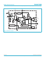
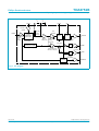
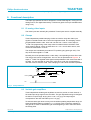
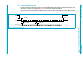
TDA8752B Triple high-speed Analog-to-Digital Converter 110 Msps Rev. 03 — 21 July 2000 Product specification 1. General description The TDA8752B is a triple 8-bit ADC with controllable amplifiers and clamps for the digitizing of large bandwidth RGB signals. The clamp level, the gain and all other settings are controlled via a serial interface (either I2C-bus or 3-wire serial bus, selected via a logic input). The IC also includes a PLL that can be locked to the horizontal line frequency and generates the ADC clock. The PLL jitter is minimized for high resolution PC graphics applications. An external clock can also be input to the ADC. It is possible to set the TDA8752B serial bus address to four different values, when several TDA8752B ICs are used in a system, by means of the I2C-bus interface (for example, two ICs used in an odd/even configuration). 2. Features c c ■ Triple 8-bit ADC ■ Sampling rate up to 110 Msps ■ IC controllable via a serial interface, which can be either I2C-bus or 3-wire serial bus, selected via a TTL input pin ■ IC analog voltage input from 0.4 to 1.2 V (p-p) to produce a full-scale ADC input of 1 V (p-p) ■ Three clamps for programming a clamping code between −63.5 and +64 in steps of 1⁄2 LSB for RGB signals, and from +120 to +136 in steps of 1⁄2 LSB for YUV signals ■ Three controllable amplifiers: gain controlled via the serial interface to produce a full-scale resolution of 1⁄2 LSB peak-to-peak ■ Amplifier bandwidth of 250 MHz ■ Low gain variation with temperature ■ PLL controllable via the serial interface to generate the ADC clock which can be locked to a line frequency of 15 to 280 kHz ■ Integrated PLL divider ■ Programmable phase clock adjustment cells ■ Internal voltage regulators ■ TTL compatible digital inputs and outputs ■ Chip enable high-impedance ADC output TDA8752B Philips Semiconductors Triple high-speed Analog-to-Digital Converter 110 Msps ■ Power-down mode ■ Possibility to use up to four ICs in the same system when using the I2C-bus interface, or more when using the 3-wire serial bus interface ■ 1.1 W power dissipation. 3. Applications ■ ■ ■ ■ ■ RGB high-speed digitizing LCD panels drive LCD projection systems VGA and higher resolutions Using two ICs in parallel, a higher display resolution can be obtained: 200 MHz pixel frequency. 4. Quick reference data Table 1: Quick reference data Symbol Parameter Conditions Min Typ Max Unit VCCA analog supply voltage for R, G and B channels 4.75 5.0 5.25 V 4.75 5.0 5.25 V 4.75 5.0 5.25 V 4.75 5.0 5.25 V 4.75 5.0 5.25 V I2C-bus VDDD logic supply voltage for and 3-wire serial bus VCCD digital supply voltage VCCO output stages supply voltage VCCA(PLL) analog PLL supply voltage VCCO(PLL) output PLL supply voltage 4.75 5.0 5.25 V ICCA analog supply current − 120 − mA IDDD logic supply current − 1.0 − mA ICCD digital supply current − 40 − mA ICCO output stages supply current − 26 − mA ICCA(PLL) analog PLL supply current − 28 − mA ICCO(PLL) output PLL supply current − 5 − mA fclk clock frequency − − 110 MHz fref(PLL) PLL reference clock frequency 15 − 280 kHz fVCO VCO output clock frequency 12 − 110 MHz INL DC integral non-linearity from analog input to digital output; full-scale; ramp input; fclk = 110 MHz − ±0.5 ±1.5 LSB DNL DC differential non-linearity from analog input to digital output; full-scale; ramp input; fclk = 110 MHz − ±0.5 ±1.0 LSB ∆Gamp/∆T amplifier gain stability as a function of temperature Vref = 2.5 V with 100 ppm/°C maximum − − 200 ppm/°C B amplifier bandwidth −3 dB; Tamb = 25 °C 250 − − MHz tset settling time of the ADC block input signal settling plus AGC time <1 ns; Tamb = 25 °C − − 6 ns for R, G and B channels for I2C-bus and 3-wire fclk = 110 MHz; ramp input © Philips Electronics N.V. 2000. All rights reserved. 9397 750 07338 Product specification Rev. 03 — 21 July 2000 2 of 38 TDA8752B Philips Semiconductors Triple high-speed Analog-to-Digital Converter 110 Msps Table 1: Quick reference data…continued Symbol Parameter Conditions DRPLL PLL divider ratio Ptot total power dissipation jPLL(rms) maximum PLL phase jitter (RMS value) Min Typ Max Unit 100 − 4095 fclk = 110 MHz; ramp input − 1.1 − W fref = 66.67 kHz; fclk = 110 MHz − 112 − ps 5. Ordering information Table 2: Ordering information Type number TDA8752BH/8 Package Description Version QFP100 plastic quad flat package; 100 leads (lead length 1.95 mm); body 14 × 20 × 2.8 mm SOT317-2 110 © Philips Electronics N.V. 2000. All rights reserved. 9397 750 07338 Product specification Sampling frequency (MHz) Name Rev. 03 — 21 July 2000 3 of 38 TDA8752B Philips Semiconductors Triple high-speed Analog-to-Digital Converter 110 Msps 6. Block diagram VCCA(R) VCCA(B) VCCO(R) VCCO(B) VCCA(PLL) VCCA(G) 11 RAGC RGAINC RIN RDEC Vref GAGC GGAINC GIN GDEC BAGC BGAINC BIN BDEC TDO TCK ADD2 ADD1 SEN SCL SDA DIS I2C/3W 19 VDDD 27 VCCO(G) 40 79 69 VCCD 59 VCCO(PLL) 95 99 AGNDG CLP 85 AGNDR 89 13 VSSD AGNDB 21 29 OGNDG AGNDPLL OGNDR 41 DGND OGNDB OGNDPLL 70 60 48 96 82 86 6 9 8 7 12 71 to 78 CLAMP 10 RCLP RBOT R0 to R7 MUX OUTPUTS 45 ADC 3 ROR RED CHANNEL 14 17 16 15 20 61 to 68 46 22 87 25 24 23 28 49, 52 to 58 BLUE CHANNEL 26 GBOT G0 to G7 GREEN CHANNEL 18 GCLP 47 GOR OE BCLP BBOT B0 to B7 BOR 36 84 35 HSYNCI 34 33 TDA8752B 81 SERIAL INTERFACE I2C-BUS OR 3-WIRE 38 42 39 83 80 REGULATOR 92 PLL 91 I2C-bus; 1-bit (Hlevel) 37 32 93 94 1, 5, 30, 31, 43 , 44 50, 51, 100 90 4 2 88 97 CKADCO CKBO CKAO CKREFO CKEXT INV COAST CKREF 98 FCE467 n.c. HSYNC DEC1 DEC2 PWDWN CP CZ Fig 1. Block diagram. © Philips Electronics N.V. 2000. All rights reserved. 9397 750 07338 Product specification Rev. 03 — 21 July 2000 4 of 38 TDA8752B Philips Semiconductors Triple high-speed Analog-to-Digital Converter 110 Msps CLP RCLP RAGC CLAMP CONTROL VP DAC 150 kΩ RIN CLKADC 8 MUX Vref ADC AGC REGISTER I2C-bus: 8 bits (Or) VCCAR 3 kΩ ROR OUTPUTS 8 R0 to R7 8 45 kΩ D DAC OE D≥R R 5 1 8 RBOT 7 REGISTER FINE GAIN ADJUST 1 I2C-bus: 5 bits (Fr) REGISTER COARSE GAIN ADJUST I2C-bus: 7 bits (Cr) I2C-BUS FCE468 RGAINC HSYNCI Fig 2. Red channel diagram. © Philips Electronics N.V. 2000. All rights reserved. 9397 750 07338 Product specification Rev. 03 — 21 July 2000 5 of 38 TDA8752B Philips Semiconductors Triple high-speed Analog-to-Digital Converter 110 Msps CP CZ COAST CZ CKEXT INV MUX 0°/180° CP I2C-bus; 1 bit (Vlevel) CKREF PHASE FREQUENCY edge selector DETECTOR I2C-bus; 1 bit I2C-bus; 5 bits (Edge) (Ip, Up, Do) 12 to 100 MHz loop filter I2C-bus; 3 bits (Z) VCO I2C-bus; phase selector A 2 bits (Vco) I2C-bus; I2C-bus; 5 bits (Pa) 1 bit (Cka) CLKADC MUX DIV N (100 to 4095) I2C-bus; 12 bits (Di) CKADCO CKBO I2C-bus; 1 bit (Ckb) phase selector B I2C-bus; 5 bits (Pb) NCKBO MUX CKAO I2C-bus; 1 bit (Ckab) CKREFO SYNCHRO FCE465 Fig 3. PLL diagram. © Philips Electronics N.V. 2000. All rights reserved. 9397 750 07338 Product specification Rev. 03 — 21 July 2000 6 of 38 TDA8752B Philips Semiconductors Triple high-speed Analog-to-Digital Converter 110 Msps 7. Pinning information 82 OGNDPLL 81 CKAO 83 CKBO 85 VCCO(PLL) 84 CKADCO 86 DGND 87 OE 88 PWDWN 89 CLP 90 HSYNC 91 INV 92 CKEXT 93 COAST 94 CKREF 96 AGNDPLL 95 VCCD 97 CP 99 VCCA(PLL) 98 CZ 100 n.c. 7.1 Pinning n.c. 1 80 CKREFO DEC2 2 Vref DEC1 3 79 VCCO(R) 78 R7 4 77 R6 n.c. 5 76 R5 RAGC 6 75 R4 RBOT 7 74 R3 RGAINC 8 73 R2 RCLP 9 72 R1 RDEC 10 71 R0 VCCA(R) 11 RIN 12 70 OGNDR 69 VCCO(G) AGNDR 13 GAGC 14 68 G7 67 G6 GBOT 15 66 G5 TDA8752BH GGAINC 16 65 G4 GCLP 17 64 G3 GDEC 18 63 G2 VCCA(G) 19 GIN 20 62 G1 61 G0 AGNDG 21 BAGC 22 60 OGNDG 59 VCCO(B) BBOT 23 58 B7 BGAINC 24 57 B6 BCLP 25 56 B5 BDEC 26 55 B4 VCCA(B) 27 BIN 28 54 B3 AGNDB 29 n.c. 30 52 B1 53 B2 n.c. 50 OGNDB 48 B0 49 BOR 47 GOR 46 ROR 45 n.c. 44 n.c. 43 SCL 42 VDDD 40 VSSD 41 SDA 39 DIS 37 SEN 38 TDO 36 TCK 35 ADD2 34 ADD1 33 n.c. 31 I2C/3W 32 51 n.c. FCE469 Fig 4. Pin configuration. © Philips Electronics N.V. 2000. All rights reserved. 9397 750 07338 Product specification Rev. 03 — 21 July 2000 7 of 38 TDA8752B Philips Semiconductors Triple high-speed Analog-to-Digital Converter 110 Msps 7.2 Pin description Table 3: Pin description Symbol Pin Description n.c. 1 not connected DEC2 2 main regulator decoupling input 2 Vref 3 gain stabilizer voltage reference input DEC1 4 main regulator decoupling input 1 n.c. 5 not connected RAGC 6 red channel AGC output RBOT 7 red channel ladder decoupling input (BOT) RGAINC 8 red channel gain capacitor input RCLP 9 red channel gain clamp capacitor input RDEC 10 red channel gain regulator decoupling input VCCA(R) 11 red channel gain analog power supply RIN 12 red channel gain analog input AGNDR 13 red channel gain analog ground GAGC 14 green channel AGC output GBOT 15 green channel ladder decoupling input (BOT) GGAINC 16 green channel gain capacitor input GCLP 17 green channel gain clamp capacitor input GDEC 18 green channel gain regulator decoupling input VCCA(G) 19 green channel gain analog power supply GIN 20 green channel gain analog input AGNDG 21 green channel gain analog ground BAGC 22 blue channel AGC output BBOT 23 blue channel ladder decoupling input (BOT) BGAINC 24 blue channel gain capacitor input BCLP 25 blue channel gain clamp capacitor input BDEC 26 blue channel gain regulator decoupling input VCCA(B) 27 blue channel gain analog power supply BIN 28 blue channel gain analog input AGNDB 29 blue channel gain analog ground n.c. 30 not connected n.c. 31 not connected I2C/3W 32 selection input between I2C-bus (active HIGH) and 3-wire serial bus (active LOW) ADD1 33 I2C-bus address control input 1 ADD2 34 I2C-bus address control input 2 TCK 35 scan test mode input (active HIGH) TDO 36 scan test output DIS 37 I2C-bus and 3-wire serial bus disable control input (disable at HIGH level) SEN 38 select enable for 3-wire serial bus input (see Figure 10) © Philips Electronics N.V. 2000. All rights reserved. 9397 750 07338 Product specification Rev. 03 — 21 July 2000 8 of 38 TDA8752B Philips Semiconductors Triple high-speed Analog-to-Digital Converter 110 Msps Table 3: Pin description…continued Symbol Pin Description SDA 39 I2C-bus/3-wire serial bus data input VDDD 40 logic I2C-bus/3-wire serial bus digital power supply VSSD 41 logic I2C-bus/3-wire serial bus digital ground SCL 42 I2C-bus/3-wire serial bus clock input n.c. 43 not connected n.c. 44 not connected ROR 45 red channel ADC output bit out of range GOR 46 green channel ADC output bit out of range BOR 47 blue channel ADC output bit out of range OGNDB 48 blue channel ADC output ground B0 49 blue channel ADC output bit 0 (LSB) n.c. 50 not connected n.c. 51 not connected B1 52 blue channel ADC output bit 1 B2 53 blue channel ADC output bit 2 B3 54 blue channel ADC output bit 3 B4 55 blue channel ADC output bit 4 B5 56 blue channel ADC output bit 5 B6 57 blue channel ADC output bit 6 B7 58 blue channel ADC output bit 7 (MSB) VCCO(B) 59 blue channel ADC output power supply OGNDG 60 green channel ADC output ground G0 61 green channel ADC output bit 0 (LSB) G1 62 green channel ADC output bit 1 G2 63 green channel ADC output bit 2 G3 64 green channel ADC output bit 3 G4 65 green channel ADC output bit 4 G5 66 green channel ADC output bit 5 G6 67 green channel ADC output bit 6 G7 68 green channel ADC output bit 7 (MSB) VCCO(G) 69 green channel ADC output power supply OGNDR 70 red channel ADC output ground R0 71 red channel ADC output bit 0 (LSB) R1 72 red channel ADC output bit 1 R2 73 red channel ADC output bit 2 R3 74 red channel ADC output bit 3 R4 75 red channel ADC output bit 4 R5 76 red channel ADC output bit 5 R6 77 red channel ADC output bit 6 R7 78 red channel ADC output bit 7 (MSB) VCCO(R) 79 red channel ADC output power supply © Philips Electronics N.V. 2000. All rights reserved. 9397 750 07338 Product specification Rev. 03 — 21 July 2000 9 of 38 TDA8752B Philips Semiconductors Triple high-speed Analog-to-Digital Converter 110 Msps Table 3: Pin description…continued Symbol Pin Description CKREFO 80 reference output clock re-synchronized horizontal pulse CKAO 81 PLL clock output 3 (in phase with reference output clock CKAO or CKBO) OGNDPLL 82 PLL digital ground CKBO 83 PLL clock output 2 CKADCO 84 PLL clock output 1 (in phase with internal ADC clock) VCCO(PLL) 85 PLL output power supply DGND 86 digital ground OE 87 output enable; active LOW (when OE is HIGH, the outputs are in high-impedance) PWDWN 88 power-down control input (device is in Power-down mode when this pin is HIGH) CLP 89 clamp pulse input (clamp active HIGH) HSYNC 90 horizontal synchronization input pulse INV 91 PLL clock output inverter command input (invert when HIGH) CKEXT 92 external clock input COAST 93 PLL coast command input CKREF 94 PLL reference clock input VCCD 95 digital power supply AGNDPLL 96 PLL analog ground CP 97 PLL filter input CZ 98 PLL filter input VCCA(PLL) 99 PLL analog power supply n.c. 100 not connected © Philips Electronics N.V. 2000. All rights reserved. 9397 750 07338 Product specification Rev. 03 — 21 July 2000 10 of 38 TDA8752B Philips Semiconductors Triple high-speed Analog-to-Digital Converter 110 Msps 8. Functional description This triple high-speed 8-bit ADC is designed to convert RGB signals, coming from an analog source, into digital data used by a LCD driver (pixel clock up to 200 MHz when using 2 ICs). 8.1 IC analog video inputs The video inputs are internally DC polarized. These inputs are AC coupled externally. 8.2 Clamps Three independent parallel clamping circuits are used to clamp the video input signals on the black level and to control the brightness level. The clamping code is programmable between code −63.5 and +64 and from +120 to +136 in steps of 1⁄ LSB. The programming of the clamp value is achieved via an 8-bit DAC. Each 2 clamp must be able to correct an offset from ±0.1 V to ±10 mV within 300 ns, and correct the total offset in 10 lines. The clamps are controlled by an external TTL positive going pulse (pin CLP). The drop of the video signal is <1 LSB. Normally, the circuit operates with a 0 code clamp, corresponding to the 0 ADC code. This clamp code can be changed from −63.5 to +64 as represented in Figure 5, in steps of 1⁄2 LSB. The digitized video signal is always between code 0 and code 255 of the ADC. It is also possible to clamp from code 120 to code 136 corresponding to 120 ADC code to 136 ADC code. Then clamping on code 128 of the ADC is possible. 255 digitized video signal = 120 to 136 code 64 code 0 code −63.5 clamp programming video signal CLP FCE471 Fig 5. Clamp definition. 8.3 Variable gain amplifiers Three independent variable gain amplifiers are used to provide, to each channel, a full-scale input range signal to the 8-bit ADC. The gain adjustment range is designed so that for an input range varying from 0.4 to 1.2 V (p-p), the output signal corresponds to the ADC full-scale input of 1 V (p-p). To ensure that the gain does not vary over the whole operating temperature range, an external supplied reference voltage Vref = 2.5 V (DC), with a maximum variation of 100 ppm/°C, is used to calibrate the gain at the beginning of each video line before the clamp pulse. © Philips Electronics N.V. 2000. All rights reserved. 9397 750 07338 Product specification Rev. 03 — 21 July 2000 11 of 38 TDA8752B Philips Semiconductors Triple high-speed Analog-to-Digital Converter 110 Msps The calibration of the gains is done using the following principle. From the reference voltage Vref a reference signal of 0.156 V (p-p) (1⁄16Vref) is generated internally. During the synchronization part of the video line, the multiplexer, controlled by the TTL synchronization signal (HSYNCI, coming from HSYNC; see Figure 1) with a width equal to one of the video synchronization signals (e.g. the signal coming from a synchronization separator), is switched between the two amplifiers. The output of the multiplexer is either the normal video signal or the 0.156 V reference signal (during HSYNC). The corresponding ADC outputs are then compared to a preset value loaded in a register. Depending on the result of the comparison, the gain of the variable gain amplifiers is adjusted (coarse gain control; see Figure 2 and 6). The three 7-bit registers receive data via a serial interface to enable the gain to be programmed. The preset value loaded in the 7-bit register is chosen between approximately 67 codes to ensure the full-scale input range (see Figure 6). A contrast control can be achieved using these registers. In this case care should be taken to stay within the allowed code range (32 to 99). A fine correction using three 5-bit DACs, also controlled via the serial interface, is used to fine tune the gain of the three channels (fine gain control; see Figure 2 and 7) and to compensate the channel-to-channel gain mismatch. With a full-scale ADC input, the resolution of the fine register corresponds to 1⁄2 LSB peak-to-peak variation. To use these gain controls correctly, it is recommended to fix the coarse gain (to have a full-scale ADC input signal) to within 4 LSB and then adjust it with the fine gain. The gain is adjusted during HSYNC. During this time the output signal is not related to the amplified input signal. The outputs, when the coarse gain system is stable, are related to the programmed coarse code (see Figure 6). NCOARSE code 127 coarse register value (67 codes) ADC output code G(max) 255 G(min) 99 227 32 160 128 0 0.156 = Vref 0.2 16 0.6 Vi (p-p) 2 FCE472 Fig 6. Coarse gain control. © Philips Electronics N.V. 2000. All rights reserved. 9397 750 07338 Product specification Rev. 03 — 21 July 2000 12 of 38 TDA8752B Philips Semiconductors Triple high-speed Analog-to-Digital Converter 110 Msps ADC output code GNCOARSE 255 G(max) G(min) 227 coarse register value (67 codes) NCOARSE 160 128 NFINE = 0 NFINE = 31 Vref FCE473 Fig 7. Fine gain correction for a coarse gain GNCOARSE. 8.4 ADCs The ADCs are 8-bit with a maximum clock frequency of 110 Msps. The ADCs input range is 1 V (p-p) full-scale. One out of range bit exists per channel (ROR, GOR and BOR). It will be at logic 1 when the signal is out of range of the full-scale of the ADCs. Pipeline delay in the ADCs is 1 clock cycle from sampling to data output. The ADCs reference ladders regulators are integrated. 8.5 ADC outputs ADC outputs are straight binary. An output enable pin (OE; active LOW) enables the output status between active and high-impedance (OE = HIGH) to be switched; it is recommended to load the outputs with a 10 pF capacitive load. The timing must be checked very carefully if the capacitive load is more than 10 pF. 8.6 Phase-locked loop The ADCs are clocked either by an internal PLL locked to the CKREF clock (all of the PLL is on-chip except the loop filter capacitance) or by an external clock applied to pin CKEXT. Selection is performed via the serial interface bus. The reference clock (CKREF) range is between 15 and 280 kHz. Consequently, the VCO minimum frequency is 12 MHz and the maximum frequency is 110 MHz. The gain of the VCO part can be controlled via the serial interface, depending on the frequency range to which the PLL is locked. To increase the bandwidth of the PLL, the charge pump current, controlled by the serial interface, must also be increased. The relationship between the frequency and the current is given by the following equation: KO ⋅ IP 1 f n = ------ ⋅ -------------------------------------2π ( C Z + C P ) ⋅ DR © Philips Electronics N.V. 2000. All rights reserved. 9397 750 07338 Product specification (1) Rev. 03 — 21 July 2000 13 of 38 TDA8752B Philips Semiconductors Triple high-speed Analog-to-Digital Converter 110 Msps Where: fn = the natural PLL frequency KO = the VCO gain DR = PLL divider ratio CZ and CP = capacitors of the PLL filter. The other PLL equation is as follows: 1 1 fn f z = ------------------------------ and ξ = --- × ----- 2π × R × C Z 2 f z (2) Where: fz = loop filter zero frequency R = the chosen resistance for the filter ξ = the damping factor FO = 0 dB loop gain frequency. Different resistances for the filter can be programmed via the serial interface. To improve the performances, the PLL parameters should be chosen so that: 2π × DR × F O F O = 2ξ ⋅ f n ⇒ R ⋅ I P = ---------------------------------KO (3) FO 0.3π × DR × f ref ---------- ≤ 0.15 ⇒ R ⋅ I P ≤ ------------------------------------------ = Lim f ref KO (4) The values of R and IP must be chosen so that the product is the closest to Lim. In the event that there are several choices, the couple for which the ξ value is the closest to 1 must be chosen. A software program called “PLL calculator’” is available on Philips Semiconductor Internet site to calculate the best PLL parameters. It is possible to control (independently) the phase of the ADC clock and the phase of an additional clock output (which could be used to drive a second TDA8752B). For this, two serial interface-controlled digital phase-shift controllers are included (controlled by 5-bit registers, phase-shift controller steps are 11.25 deg each on the whole PLL frequency range). CKREF is re-synchronized, by the synchro block, on the CKAO clock. The output is CKREFO (LOW during 8 clock periods). CKAO is the clock at the output of the phase selector A. This clock can be used as the clocks for CKBO and CKADCO. The timing is given in Figure 8. Pin COAST is used to disconnect the PLL phase frequency detector during the frame flyback or the unavailability of the CKREF signal. This signal can normally be derived from the VSYNC signal. The clock output is able to drive an external 10 pF load (for the on-chip ADCs). © Philips Electronics N.V. 2000. All rights reserved. 9397 750 07338 Product specification Rev. 03 — 21 July 2000 14 of 38 TDA8752B Philips Semiconductors Triple high-speed Analog-to-Digital Converter 110 Msps The PLL can be used in three different methods: • The IC can be used as stand-alone with a sampling frequency of up to 110 MHz. • When an RGB signal is at a pixel frequency exceeding 100 to 200 MHz, it is possible to follow one of the two possibilities given below: – Using one TDA8752B: the sampling rate can be reduced by a factor of two, by sampling the even pixels in the even frame and the odd pixels in the odd frame. Pin INV is used to toggle between the frames. – Using two TDA8752Bs: the PLL of the master TDA8752B is used to drive both ADC clocks. The PLL of the slave TDA8752B is disconnected and the CKBO of the master TDA8752B is connected to pin CKEXT of the TDA8752B master and CKAO to the slave TDA8752B. In this case, on pin CKAO CKBO will be the output (with bit CKAB of the master at logic 1). The master TDA8752B is used to sample the even pixels and the slave TDA8752B for odd pixels, using a 180 deg phase shift between the clocks (both pins CKADCO). The master chip and the slave chip have their pin INV LOW, which guarantees the 180 deg shift ADC clock drive. It is then necessary to adjust phase B of the master chip. Special care should be taken with the quality of the input signal (input settling time). If CKREFO output signal at the master chip is needed, it is possible to use one of the two phase A values in order to avoid set-up and hold problems in the SYNCHRO function; e.g. PHASEA = 100000 and PHASEA = 111111. • When INV is LOW, CKADCO is equal to CKEXT inverted. CKREF CKAO tCKAO CKREFO tCKREFO FCE470 t phase selector tCKAO = tCLK(buffer) + tphase selector [tCLK(buffer) = 10 ns and tphase selector = --------------------------- × T CLK(pixel) ]. 2π T CLK(pixel) T CLK(pixel) tCKREFO = either tCKAO − ------------------------ if PHASEA ≥ 01000 or tCKAO + ------------------------ if PHASEA < 01000. 2 2 Fig 8. Timing diagram. © Philips Electronics N.V. 2000. All rights reserved. 9397 750 07338 Product specification Rev. 03 — 21 July 2000 15 of 38 TDA8752B Philips Semiconductors Triple high-speed Analog-to-Digital Converter 110 Msps COAST CKEXT INV 12 to 100 MHz MUX CKADCO 0 /180 phase selector A I2C-bus; I2C-bus; 5 bits (Pa) 1 bit (Cka) (Cka = 1) CLKADC CKBO MUX CKREF PLL I2C-bus; 1 bit (Ckb) (Ckb = 1) phase selector B I2C-bus; 5 bits (Pb) NCKBO CKAO MUX Master TDA8752B (even pixels) I2C-bus; 1 bit (Ckab) (Ckab = 1) SYNCHRO CKEXT COAST CKREFO INV 12 to 100 MHz MUX CKADCO 0 /180 phase selector A I2C-bus; I2C-bus; 5 bits (Pa) 1 bit (Cka) (Cka = 1) CLKADC MUX CKREF PLL CKBO I2C-bus; 1 bit (Ckb) (Ckb = 0) phase selector B I2C-bus; 5 bits (Pb) NCKBO CKAO MUX Slave TDA8752B (odd pixels) I2C-bus; 1 bit (Ckab) (Ckab = 0) SYNCHRO CKREFO FCE466 Slave at 180 deg phase shift with respect to pin CKADCO of the master TDA8752B. Fig 9. Dual TDA8752B solution for pixel clock rate with a single phase adjustment (100 to 200 MHz). 8.7 I2C-bus and 3-wire serial bus interface The I2C-bus and 3-wire serial buses control the status of the different control DACs and registers. Control pin DIS enables or disables the full serial interface function (disable at HIGH level). Four ICs can be used in the same system and programmed by the same bus. Therefore, two pins (ADD1 and ADD2) are available to set each address respectively, for use with the I2C-bus interface. All programming is described in Section 9 “I2C-bus and 3-wire serial bus interfaces”. © Philips Electronics N.V. 2000. All rights reserved. 9397 750 07338 Product specification Rev. 03 — 21 July 2000 16 of 38 TDA8752B Philips Semiconductors Triple high-speed Analog-to-Digital Converter 110 Msps 9. I2C-bus and 3-wire serial bus interfaces 9.1 Register definitions The configuration of the different registers is shown in Table 4. Table 4: Function name I2C-bus and 3-wire serial bus registers Subaddress Bit definition A7 A6 A5 A4 A3 A2 A1 A0 MSB LSB Default value SUBADDR − − − − − − − − X X X Mode Sa3 Sa2 Sa1 Sa0 XXX1 0000 OFFSETR X X X X 0 0 0 0 Or7 Or6 Or5 Or4 Or3 Or2 Or1 Or0 0111 1111 COARSER X X X X 0 0 0 1 Or8 Cr6 Cr5 Cr4 Cr3 Cr2 Cr1 Cr0 0010 0000 FINER X X X X 0 0 1 0 X X X Fr4 Fr3 Fr2 Fr1 Fr0 XXX0 0000 OFFSETG X X X X 0 0 1 1 Og7 Og6 Og5 Og4 Og3 Og2 Og1 Og0 0111 1111 COARSEG X X X X 0 1 0 0 Og8 Cg6 Cg5 Cg4 Cg3 Cg2 Cg1 Cg0 0010 0000 FINEG X X X X 0 1 0 1 X X X Fg4 Fg3 Fg2 Fg1 Fg0 XXX0 0000 OFFSETB X X X X 0 1 1 0 Ob7 Ob6 Ob5 Ob4 Ob3 Ob2 Ob1 Ob0 0111 1111 COARSEB X X X X 0 1 1 1 Ob8 Cb6 Cb5 Cb4 Cb3 Cb2 Cb1 Cb0 0010 0000 FINEB X X X X X 1 0 0 0 X X Fb4 Fb3 Fb2 Fb1 Fb0 XXX0 0000 CONTROL X X X X 1 0 0 1 Vlevel Hlevel Edge Up Do Ip2 Ip1 Ip0 0000 0100 VCO X X X X 1 0 1 0 Z2 Z1 Z0 Vco1 Vco0 Di11 Di10 Di9 0110 0001 DIVIDER (LSB) X X X X 1 0 1 1 Di8 Di7 Di6 Di5 Di4 Di3 Di2 Di1 1001 0000 PHASEA X X X X 1 1 0 0 X Di0 Cka Pa4 Pa3 Pa2 Pa1 Pa0 X000 0000 PHASEB X X X X 1 1 0 1 X Ckab Ckb Pb4 Pb3 Pb2 Pb1 Pb0 X000 0000 All the registers are defined by a subaddress of 8 bits; bit A4 refers to the mode which is used with the I2C-bus interface; bits Sa3 to Sa0 are the subaddresses of each register. Bit Mode, used only with the I2C-bus, enables two modes to be programmed: 9.1.1 Mode 0 if bit Mode = 0, each register is programmed independently by giving its subaddress and its content Mode 1 if bit Mode = 1, all the registers are programmed one after the other by giving this initial condition (XXX1 1111) as the subaddress state; thus, the registers are charged following the predefined sequence of 16 bytes (from subaddress 0000 to 1101). Offset register This register controls the clamp level for the RGB channels. The relationship between the programming code and the level of the clamp code is given in Table 5. © Philips Electronics N.V. 2000. All rights reserved. 9397 750 07338 Product specification Rev. 03 — 21 July 2000 17 of 38 TDA8752B Philips Semiconductors Triple high-speed Analog-to-Digital Converter 110 Msps Table 5: Coding Programmed code Clamp code ADC output 0 −63.5 underflow 1 −63 2 −62.5 ... ... 127 0 0 ... ... ... 254 63.5 63 or 64 255 64 64 256 120 120 ... ... ... 287 136 136 The default programmed value is: • Programmed code = 127 • Clamp code = 0 • ADC output = 0. 9.1.2 Coarse and fine registers These two registers enable the gain control, the AGC gain with the coarse register and the reference voltage with the fine register. The coarse register programming equation is as follows: N COARSE + 1 N COARSE + 1 1 GAIN = ------------------------------------------------ × ------ = -------------------------------------------------- × 32 V ref ⋅ ( 512 – N FINE ) N FINE 16 V ref ⋅ 1 – ----------------- 32 × 16 (5) Where: Vref = 2.5 V. The gain correspondence is given in Table 6. The gain is linear with reference to the programming code (NFINE = 0). Table 6: Gain correspondence (COARSE) NCOARSE Gain Vi to be full-scale (V) 32 0.825 1.212 99 2.5 0.4 The default programmed value is as follows: • NCOARSE = 32 • Gain = 0.825 • Vi to be full-scale = 1.212 V. To modulate this gain, the fine register is programmed using the above equation. With a full-scale ADC input, the fine register resolution is a 1⁄2 LSB peak-to-peak (see Table 7 for NCOARSE = 32). © Philips Electronics N.V. 2000. All rights reserved. 9397 750 07338 Product specification Rev. 03 — 21 July 2000 18 of 38 TDA8752B Philips Semiconductors Triple high-speed Analog-to-Digital Converter 110 Msps Table 7: Gain correspondence (FINE) NFINE Gain Vi to be full-scale (V) 0 0.825 1.212 31 0.878 1.139 The default programmed value is: NFINE = 0. 9.1.3 Control register COAST and HSYNC signals can be inverted by setting the I2C-bus control bits ‘Vlevel’ and ‘Hlevel’ respectively. When ‘Vlevel’ and ‘Hlevel’ are set to zero respectively, COAST and HSYNC are active HIGH. The bit ‘Edge’ defines the rising or falling edge of CKREF to synchronize the PLL. It will be on the rising edge if the bit is at logic 0 and on the falling edge if the bit is at logic 1. The bits ‘Up’ and ‘Do’ are used for the test, to force the charge pump current. These bits have to be logic 0 during normal use. The bits ‘Ip0’, ‘Ip1’ and ‘Ip2’ control the charge pump current, to increase the bandwidth of the PLL, as shown in Table 8. Table 8: Charge pump current control Ip2 Ip1 Ip0 Current (µA) 0 0 0 6.25 0 0 1 12.5 0 1 0 25 0 1 1 50 1 0 0 100 1 0 1 200 1 1 0 400 1 1 1 700 The default programmed value is as follows: • • • • 9.1.4 Charge pump current = 100 µA Test bits: no test mode; bits ‘Up’ and ‘Do’ at logic 0 Rising edge of CKREF: bit ‘Edge’ at logic 0 COAST and HSYNC inputs are active HIGH: bits ‘Vlevel’ and ‘Hlevel’ at logic 0. VCO register The bits ‘Z2’, ‘Z1’ and ‘Z0’ enable the internal resistance for the VCO filter to be selected. © Philips Electronics N.V. 2000. All rights reserved. 9397 750 07338 Product specification Rev. 03 — 21 July 2000 19 of 38 TDA8752B Philips Semiconductors Triple high-speed Analog-to-Digital Converter 110 Msps Table 9: VCO register bits Z2 Z1 Z0 Resistance (kΩ) 0 0 0 high impedance 0 0 1 128 0 1 0 32 0 1 1 16 1 0 0 8 1 0 1 4 1 1 0 2 1 1 1 1 Table 10: VCO gain control Vco1 Vco0 VCO gain (MHz/V) Pixel clock frequency range (MHz) 0 0 15 10 to 20 0 1 20 20 to 40 1 0 35 40 to 70 1 1 50 70 to 110 The bits Vco1 and Vco0 control the VCO gain. The default programmed value is as follows: • Internal resistance = 16 kΩ • VCO gain = 15 MHz/V. © Philips Electronics N.V. 2000. All rights reserved. 9397 750 07338 Product specification Rev. 03 — 21 July 2000 20 of 38 TDA8752B Philips Semiconductors Triple high-speed Analog-to-Digital Converter 110 Msps 9.1.5 Divider register This register controls the PLL frequency. The bits are the LSB bits. The default programmed value is 0011 0010 0000 = 800. The MSB bits (Di11, Di10 and Di9) and the LSB bit (Di0) have to be programmed before bits ‘Di8’ to ‘Di1’ are programmed, to obtain the required divider ratio. Bit ‘Di0’ is used for the parity divider number (bit ‘Di0’ = 0 means even number, while bit ‘Di0’ = 1 means odd number). It should be noted that if the I2C-bus programming is done in mode 1 (bit Mode = 1) and bit ‘Di0’ has to be toggled, then the registers have to be loaded twice to have the update divider ratio. 9.1.6 Power-down mode • When the supply is completely switched off, the registers are set to their default values; in that event they have to be reprogrammed if the required settings are different (e.g. through an EEPROM) • When the device is in Power-down mode, the previously programmed register values remain unaffected. 9.1.7 PHASEA and PHASEB registers Bit ‘Cka’ is logic 0 when the used clock is the PLL clock, and logic 1 when the used clock is the external clock. Bit ‘Ckb’ is logic 0 when the second clock is not used. Bits ‘Pa4’ to ‘Pa0’ and bits ‘Pb4’ to ‘Pb0’ are used to program the phase shift for the clock, CKADCO, CKAO and CKBO (see Table 11). Concerning the PHASEB register, bit ‘Ckab’ is used to have either CKAO or CKBO at pin CKAO (pin 81). Table 11: Phase registers bits Pa4 and Pb4 Pa3 and Pb3 Pa2 and Pb2 Pa1 and Pb1 Pa0 and Pb0 Phase shift (deg) 0 0 0 0 0 0 0 0 0 0 1 11.25 ... ... ... ... ... ... 1 1 1 1 0 337.5 1 1 1 1 1 348.75 The default programmed value is as follows: • • • • • No external clock: bit ‘Cka’ is logic 0 No use of the second clock: bit ‘Ckb’ is logic 0 Phase shift for CKAO and CKADCO is 0 deg Phase shift for CKBO is 0 deg Clock CKAO at pin CKAO: bit ‘Ckab’ is logic 0. © Philips Electronics N.V. 2000. All rights reserved. 9397 750 07338 Product specification Rev. 03 — 21 July 2000 21 of 38 TDA8752B Philips Semiconductors Triple high-speed Analog-to-Digital Converter 110 Msps 9.2 I2C-bus protocol Table 12: I2C-bus address A7 A6 A5 A4 A3 A2 A1 A0 1 0 0 1 1 ADD2 ADD1 0 The I2C-bus address of the circuit is 1001 1xx0. Bits ‘A2’ and ‘A1’ are fixed by the potential on pins ADD1 and ADD2. Thus, four TDA8752Bs can be used on the same system, using the addresses for ADD1 and ADD2 with the I2C-bus. Bit ‘A0’ must always be equal to logic 0 because it is not possible to read the data in the register. The timing and protocol for the I2C-bus are standard. Two sequences are available, see Table 13 and 14. Table 13: Address sequence for mode 0 Where: S = START condition, ACK = acknowledge and P = STOP condition. S IC ADDRESS ACK SUBADDRESS REGISTER1 ACK DATA REGISTER1 (see Table 4) ACK SUBADDRESS REGISTER2 ACK ... P ACK DATA REGISTER2 ACK ... P Table 14: Address sequence for mode 1 Where: S = START condition, ACK = acknowledge and P = STOP condition. S IC ADDRESS ACK SUBADDRESS XXX1 1111 ACK DATA REGISTER1 (see Table 4) © Philips Electronics N.V. 2000. All rights reserved. 9397 750 07338 Product specification Rev. 03 — 21 July 2000 22 of 38 Philips Semiconductors 9397 750 07338 Product specification 9.3 3-wire serial bus protocol For the 3-wire serial bus the first byte refers to the register address which is programmed. The second byte refers to the data to be sent to the chosen register (see Table 4). The acquisition is achieved via SEN. Using the 3-wire serial bus interface, an indefinite number of ICs can operate on the same system. Pin SEN is used to validate the circuits. SEN tr3W = 600 ns 100 ns 1 9 1 9 SCL ts3W = 100 ns X Fig 10. 3-wire serial bus protocol. X X X A3 A2 A1 A0 X D7 D6 D5 D4 D3 D2 D1 D0 X FCE474 TDA8752B 23 of 38 © Philips Electronics N.V. 2000. All rights reserved. Triple high-speed Analog-to-Digital Converter 110 Msps Rev. 03 — 21 July 2000 SDA th3W = 100 ns TDA8752B Philips Semiconductors Triple high-speed Analog-to-Digital Converter 110 Msps 10. Limiting values Table 15: Limiting values In accordance with the Absolute Maximum Rating System (IEC 60134). Symbol Parameter VCCA Conditions Min Max Unit analog supply voltage −0.3 +7.0 V VCCD digital supply voltage −0.3 +7.0 V VDDD logic supply voltage −0.3 +7.0 V VCCO output stages supply voltage −0.3 +7.0 V ∆VCC supply voltage differences VCCA − VCCD −1.0 +1.0 V VCCO − VCCD; VCCO − VDDD −1.0 +1.0 V VCCA − VDDD; VCCD − VDDD −1.0 +1.0 V VCCA − VCCO −1.0 +1.0 V −0.3 +7.0 V Vi(RGB) RGB input voltage range referenced to AGND Io output current − 10 mA II(OE) input current pin OE − 1.0 mA II(PWDWN) input current pin PWDWN − 1.0 mA Tstg storage temperature −55 +150 °C Tamb ambient temperature 0 70 °C Tj junction temperature − 150 °C 11. Thermal characteristics Table 16: Thermal characteristics Symbol Parameter Conditions Value Unit Rth(j-a) thermal resistance from junction to ambient in free air 52 K/W 12. Characteristics Table 17: Characteristics VCCA = V11 (or V19, V27 or V99) referenced to AGND (V13, V21, V29 or V96) = 4.75 to 5.25 V; VCCD = V95 referenced to DGND (V86) = 4.75 to 5.25 V; VDDD = V40 referenced to VSSD (V41) = 4.75 to 5.25 V; VCCO = V59 (or V69, V79 or V85) referenced to OGND (V48, V60, V70 or V82) = 4.75 to 5.25 V; AGND, DGND, OGND and VSSD connected together; Tamb = 0 to 70 °C; typical values measured at VCCA = VDDD = VCCD = VCCO = 5 V and Tamb = 25 °C; unless otherwise specified. Symbol Parameter Conditions Min Typ Max Unit Supplies VCCA analog supply voltage 4.75 5.0 5.25 V VCCD digital supply voltage 4.75 5.0 5.25 V VDDD logic supply voltage 4.75 5.0 5.25 V VCCO output stages supply voltage 4.75 5.0 5.25 V ICCA analog supply current − 120 − mA © Philips Electronics N.V. 2000. All rights reserved. 9397 750 07338 Product specification Rev. 03 — 21 July 2000 24 of 38 TDA8752B Philips Semiconductors Triple high-speed Analog-to-Digital Converter 110 Msps Table 17: Characteristics…continued VCCA = V11 (or V19, V27 or V99) referenced to AGND (V13, V21, V29 or V96) = 4.75 to 5.25 V; VCCD = V95 referenced to DGND (V86) = 4.75 to 5.25 V; VDDD = V40 referenced to VSSD (V41) = 4.75 to 5.25 V; VCCO = V59 (or V69, V79 or V85) referenced to OGND (V48, V60, V70 or V82) = 4.75 to 5.25 V; AGND, DGND, OGND and VSSD connected together; Tamb = 0 to 70 °C; typical values measured at VCCA = VDDD = VCCD = VCCO = 5 V and Tamb = 25 °C; unless otherwise specified. Symbol Parameter IDDD Min Typ Max Unit logic supply current for I2C-bus and 3-wire serial bus − 1.0 − mA ICCD digital supply current − 40 − mA ICCO output stages supply current ramp input; fclk = 110 MHz − 26 − mA ICCO(PLL) output PLL supply current − 5 − mA ICCA(PLL) analog PLL supply current − 28 − mA ∆VCC supply voltage differences VCCA − VCCD −0.25 − +0.25 V VCCO − VCCD; VCCO − VDDD −0.25 − +0.25 V VCCA − VDDD; VCCD − VDDD −0.25 − +0.25 V VCCA − VCCO −0.25 − +0.25 V − 1.1 − W − 87 − mW Ptot total power dissipation Ppd power dissipation in Power-down mode Conditions ramp input; fclk = 110 MHz R, G and B amplifiers B bandwidth −3 dB; Tamb = 25 °C 250 − − MHz tset settling time of the block ADC plus AGC full-scale (black-to-white) transition; input signal settling time <1 ns (1 to 99%); Tamb = 25 °C − 4.5 6 ns GNCOARSE coarse gain range Vref = 2.5 V; minimum coarse gain register; code = 32 (see Figure 6) − −1.67 − dB maximum coarse gain register; code = 99 (see Figure 6) − 8 − dB fine register input code = 0 (see Figure 7) − 0 − dB fine register input code = 31 (see Figure 7) − −0.5 − dB Vref = 2.5 V with 100 ppm/°C maximum variation − − 200 ppm/°C − ±20 − µA GFINE fine gain correction range ∆Gamp/∆T amplifier gain stability as a function of temperature IGC gain current tstab amplifier gain adjustment speed HSYNC active; capacitors on pins 8, 16 and 24 = 22 nF − 25 − mdB/µs Vi(p-p) input voltage range (peak-to-peak value) corresponding to full-scale output 0.4 − 1.2 V tr(Vi) input voltage rise time fi = 110 MHz; square wave − − 2.5 ns tf(Vi) input voltage fall time fi = 110 MHz; square wave − − 2.5 ns © Philips Electronics N.V. 2000. All rights reserved. 9397 750 07338 Product specification Rev. 03 — 21 July 2000 25 of 38 TDA8752B Philips Semiconductors Triple high-speed Analog-to-Digital Converter 110 Msps Table 17: Characteristics…continued VCCA = V11 (or V19, V27 or V99) referenced to AGND (V13, V21, V29 or V96) = 4.75 to 5.25 V; VCCD = V95 referenced to DGND (V86) = 4.75 to 5.25 V; VDDD = V40 referenced to VSSD (V41) = 4.75 to 5.25 V; VCCO = V59 (or V69, V79 or V85) referenced to OGND (V48, V60, V70 or V82) = 4.75 to 5.25 V; AGND, DGND, OGND and VSSD connected together; Tamb = 0 to 70 °C; typical values measured at VCCA = VDDD = VCCD = VCCO = 5 V and Tamb = 25 °C; unless otherwise specified. Symbol Parameter Conditions Min Typ Max Unit GE(rms) channel-to-channel gain matching (RMS value) maximum coarse gain; Tamb = 25 °C − 1 − % minimum coarse gain; Tamb = 25 °C − 2 − % Clamps PCLP precision black level noise on RGB channels = 10 mV (max.) (RMS value); Tamb = 25 °C −1 − +1 LSB tCOR1 clamp correction time to within ±10 mV ±100 mV black level input variation; clamp capacitor = 4.7 nF − − 300 ns tCOR2 clamp correction time to less than 1 LSB ±100 mV black level input variation; clamp capacitor = 4.7 nF − − 10 lines tW(CLP) clamp pulse width 500 − 2000 ns CLPE channel-to-channel clamp matching −1 − +1 LSB Aoff code clamp reference clamp register input code = 0 − −63.5 − LSB clamp register input code = 255 − +64 − LSB clamp register input code = 367 − +120 − LSB clamp register input code = 398 − +136 − LSB fclk = 110 MHz; see Table 18 − 112 − ps Phase-locked loop jPLL(rms) maximum PLL phase jitter (RMS value) DR divider ratio 100 − 4095 fref reference clock frequency range 15 − 280 kHz fPLL output clock frequency range 12 − 110 MHz tCOAST(max) maximum coast mode time − − 40 lines trecap PLL recapture time when coast mode is aborted − 3 − lines tcap PLL capture time in start-up conditions − − 5 ms Φstep phase shift step Tamb = 25 °C − 11.25 − deg 110 − − MHz − ±0.5 ±1.5 LSB ADCs fs maximum sampling frequency INL DC integral non-linearity from IC analog input to digital output; ramp input; fclk = 110 MHz © Philips Electronics N.V. 2000. All rights reserved. 9397 750 07338 Product specification Rev. 03 — 21 July 2000 26 of 38 TDA8752B Philips Semiconductors Triple high-speed Analog-to-Digital Converter 110 Msps Table 17: Characteristics…continued VCCA = V11 (or V19, V27 or V99) referenced to AGND (V13, V21, V29 or V96) = 4.75 to 5.25 V; VCCD = V95 referenced to DGND (V86) = 4.75 to 5.25 V; VDDD = V40 referenced to VSSD (V41) = 4.75 to 5.25 V; VCCO = V59 (or V69, V79 or V85) referenced to OGND (V48, V60, V70 or V82) = 4.75 to 5.25 V; AGND, DGND, OGND and VSSD connected together; Tamb = 0 to 70 °C; typical values measured at VCCA = VDDD = VCCD = VCCO = 5 V and Tamb = 25 °C; unless otherwise specified. Symbol Parameter Conditions Min Typ Max Unit DNL DC differential non linearity from IC analog input to digital output; ramp input; fclk = 110 MHz − ±0.5 ±1.0 LSB ENOB effective number of bits from IC analog input to digital output; 10 kHz sine wave input; ramp input; fclk = 110 MHz − 7.4 − bits maximum gain; fclk = 110 MHz − 45 − dB minimum gain; fclk = 110 MHz − 44 − dB [1] Signal-to-noise ratio S/N signal-to-noise ratio Spurious free dynamic range SFDR spurious free dynamic range maximum gain; fclk = 110 MHz − 60 − dB minimum gain; fclk = 110 MHz − 60 − dB 45 50 55 % − − 110 MHz Clock timing output (CKADCO, CKBO and CKAO) ηext ADC clock duty cycle fclk clock frequency 100 MHz output Clock timing input (CKEXT) fclk clock frequency − − 110 MHz tCPH clock pulse width HIGH 3.6 − − ns tCPL clock pulse width LOW 4.5 − − ns td(CLKO) delay from CKEXT to CKADCO INV set to LOW 9.5 10.1 10.7 ns INV set to HIGH − 10.1 + − ns time difference between samples when operated in the same supply and temperature conditions − 0.1 0.3 ns − − − ns ∆t-td(CLKO) Data timing (see Figure 11); fclk = 110 MHz; CL = 10 pF; 1⁄ t 2 clk [2] td(s) sampling delay time referenced to CKADCO td(o) output delay time − −2 −1.5 ns th(o) output hold time 1.5 2.3 − ns 3-state output delay time (see Figure 12) tdZH output enable HIGH − 12 − ns tdZL output enable LOW − 10 − ns tdHZ output disable HIGH − 50 − ns tdLZ output disable LOW − 65 − ns Io = 1 mA − 0.3 0.4 V PLL clock output VOL LOW-level output voltage VOH HIGH-level output voltage Io = −1 mA 2.4 3.5 − V IOL LOW-level output current VOL = 0.4 V − 2 − mA IOH HIGH-level output current VOH = 2.7 V − −0.4 − mA © Philips Electronics N.V. 2000. All rights reserved. 9397 750 07338 Product specification Rev. 03 — 21 July 2000 27 of 38 TDA8752B Philips Semiconductors Triple high-speed Analog-to-Digital Converter 110 Msps Table 17: Characteristics…continued VCCA = V11 (or V19, V27 or V99) referenced to AGND (V13, V21, V29 or V96) = 4.75 to 5.25 V; VCCD = V95 referenced to DGND (V86) = 4.75 to 5.25 V; VDDD = V40 referenced to VSSD (V41) = 4.75 to 5.25 V; VCCO = V59 (or V69, V79 or V85) referenced to OGND (V48, V60, V70 or V82) = 4.75 to 5.25 V; AGND, DGND, OGND and VSSD connected together; Tamb = 0 to 70 °C; typical values measured at VCCA = VDDD = VCCD = VCCO = 5 V and Tamb = 25 °C; unless otherwise specified. Symbol Parameter Conditions Min Typ Max Unit ADC data outputs VOL LOW-level output voltage Io = 1 mA − 0 0.4 V VOH HIGH-level output voltage Io = −1 mA 2.4 VCCD − V IOL LOW-level output current VOL = 0.4 V − 2 − mA IOH HIGH-level output current VOH = 2.7 V − −0.4 − mA TTL digital inputs (CKREF, COAST, CKEXT, INV, HSYNC and CLP) VIL LOW-level input voltage − − 0.8 V VIH HIGH-level input voltage 2.0 − − V IIL LOW-level input current VIL = 0.4 V 400 − − µA IIH HIGH-level input current VIH = 2.7 V − − 100 µA Zi input impedance − 4 − kΩ Ci input capacitance − 4.5 − pF − − 0.8 V TTL digital inputs (PWDWN, OE) VIL LOW-level input voltage VIH HIGH-level input voltage II(OE) II(PWDWN) input current pin OE input current pin PWDWN 2.0 − − V with 10 kΩ resistor [3] − − 1.0 mA with 10 kΩ resistor [3] − − 1.0 mA 3-wire serial bus trst reset time of the chip before 3-wire serial bus communication − 600 − ns tsu data set-up time − 100 − ns th data hold time − 100 − ns fSCL clock frequency 0 − 100 kHz tBUF time the bus must be free before new transmission can start 4.7 − − µs tHD;STA start condition hold time 4.0 − − µs tSU;STA start condition set-up time 4.7 − − µs tCKL LOW-level clock period 4.7 − − µs tCKH HIGH-level clock period 4.0 − − µs tSU;DAT data set-up time 250 − − ns tHD;DAT data hold time 0 − − ns I2C-bus [4] repeated start tr SDA and SCL rise time fSCL = 100 kHz − − 1.0 µs tf SDA and SCL fall time fSCL = 100 kHz − − 300 ns tSU;STOP stop condition set-up time 4.0 − − µs CL(bus) bus line capacitive loading − − 400 pF © Philips Electronics N.V. 2000. All rights reserved. 9397 750 07338 Product specification Rev. 03 — 21 July 2000 28 of 38 TDA8752B Philips Semiconductors Triple high-speed Analog-to-Digital Converter 110 Msps [1] [2] [3] [4] Effective bits are obtained via a Fast Fourier Transform (FFT) treatment taking 8000 acquisition points per equivalent fundamental period. The calculation takes into account all harmonics and noise up to half clock frequency (NYQUIST frequency). Conversion-to-noise ratio: S/N = EB × 6.02 + 1.76 dB. Output data acquisition is available after the maximum delay time td(o), which is the time during which the data is available. All the timings are given for a 10 pF capacitive load. A higher load can be used but the timing must then be rechecked. The input current must be limited in accordance with the limiting values. The I2C-bus timings are given for a frequency of 100 kbit/s (100 kHz). This bus can be used at a frequency of 400 kbit/s (400 kHz). tCPH tCPL n 50 % = 1.4 V CKADCO td(o) DATA R0 to R7, ROR G0 to G7, GOR B0 to B7, BOR 2.4 V In − 1 In In + 1 1.4 V In + 2 0.4 V th(o) td(s) Vin sample N + 1 sample N + 2 FCE475 sample N Fig 11. Data timing diagram. handbook, full pagewidth V CCD 50% OE tdHZ tdZH HIGH 90% output data 50% tdLZ tdZL LOW HIGH VCCD output data 50% LOW 3.3 kΩ 10% S1 TDA8752B 10 pF OE FCE476 fOE = 100 kHz; switch S1 connected to VCCD for tdLZ and tdZL; switch S1 connected to GND for tdHZ and tdZH. Fig 12. Timing diagram and test conditions of 3-state output delay time. © Philips Electronics N.V. 2000. All rights reserved. 9397 750 07338 Product specification Rev. 03 — 21 July 2000 29 of 38 TDA8752B Philips Semiconductors Triple high-speed Analog-to-Digital Converter 110 Msps Table 18: Examples of PLL settings and performance VCCA = VDDD = VCCD = VCCO = 5 V; Tamb = 25 °C. Video standards fref (kHz) fclk (MHz) N KO CZ CP (MHz/V) (nF) (nF) IP Z Long-term time jitter [1] (µA) (kΩ) RMS-value peak-to-peak (ps) value (ns) CGA: 640 × 200 15.75 14.3 912 15 39 0.15 100 8 593 3.56 VGA: 640 × 480 31.5 25.18 800 20 39 0.15 200 4 255 1.53 VGA: 640 × 482 48.07 38.4 800 20 39 0.15 400 4 173 1.04 VESA: 800 × 600 (SVGA 72 Hz) 48.08 50 1040 35 39 0.15 200 4 200 1.2 VESA: 1024 × 768 (XGA 75 Hz) 60.02 78.75 1312 50 39 0.15 700 2 122 0.73 SUN: 1152 × 900 66.67 100 1500 50 39 0.15 400 4 115 0.69 VESA: 1280 × 1024 (SXGA 60 Hz) 63.98 108 1688 50 39 0.15 400 4 112 0.67 [1] PLL long-term time jitter is measured at the end of the video line, where it is at its maximum. © Philips Electronics N.V. 2000. All rights reserved. 9397 750 07338 Product specification Rev. 03 — 21 July 2000 30 of 38 TDA8752B Philips Semiconductors Triple high-speed Analog-to-Digital Converter 110 Msps 13. Application information PWDWN 150 pF CLP OE 39 nF CP CZ VCCA(PLL) n.c. n.c. 10 nF 2.5 V RIN GIN BIN 1 CKBO CKADCO COAST VCCO(PLL) R1 R2 CKEXT AGNDPLL HSYNC CKREF DGND VCCD INV OGNDPLL CKAO 100 99 98 97 96 95 94 93 92 91 90 89 88 87 86 85 84 83 82 81 80 DEC2 79 2 Vref 3 78 DEC1 4 77 n.c. 1.5 nF 5 76 RAGC 75 6 10 nF RBOT 7 74 22 nF RGAINC 8 73 4.7 nF RCLP 9 72 10 nF RDEC 71 10 VCCA(R) 11 70 100 nF RIN 12 69 AGNDR 13 68 75 Ω or 50 Ω GAGC 67 14 10 nF GBOT 15 66 22 nF GGAINC TDA8752B 16 65 4.7 nF GCLP 17 64 10 nF GDEC 63 18 VCCA(G) 19 62 100 nF GIN 20 61 AGNDG 21 60 75 Ω or 50 Ω BAGC 59 22 10 nF BBOT 23 58 22 nF BGAINC 24 57 4.7 nF BCLP 25 56 10 nF BDEC 55 26 VCCA(B) 27 54 100 nF BIN 28 53 AGNDB 52 29 75 Ω or 50 Ω n.c. 51 30 31 32 33 34 35 36 37 38 39 40 41 42 43 44 45 46 47 48 49 50 n.c. ADD1 TCK I2C/3W ADD2 DIS TDO SEN VDDD VSSD n.c. ROR BOR n.c. GOR 4.7 4.7 kΩ kΩ SDA SCL VDDD VDDD CKREFO VCCO(R) R7 R6 R5 R4 R3 R2 R1 R0 OGNDR VCCO(G) G7 G6 G5 G4 G3 G2 G1 G0 OGNDG VCCO(B) B7 B6 B5 B4 B3 B2 B1 n.c. B0 n.c. OGNDB FCE477 All supply pins have to be decoupled, with two capacitors: one for the high frequencies (approximately 1 nF) and one for the low frequencies (approximately 100 nF or higher). If a capacitor of 39 nF between pins CZ and CP is not available, use a higher one as close as possible to this value. Resistors R1 and R2 must be connected: the recommended value is 10 kΩ. Fig 13. Application diagram. © Philips Electronics N.V. 2000. All rights reserved. 9397 750 07338 Product specification Rev. 03 — 21 July 2000 31 of 38 TDA8752B Philips Semiconductors Triple high-speed Analog-to-Digital Converter 110 Msps 14. Package outline QFP100: plastic quad flat package; 100 leads (lead length 1.95 mm); body 14 x 20 x 2.8 mm SOT317-2 c y X 80 A 51 81 50 ZE e E HE A A2 (A 3) A1 θ wM pin 1 index Lp bp L 31 100 detail X 30 1 wM bp e ZD v M A D B HD v M B 0 5 10 mm scale DIMENSIONS (mm are the original dimensions) UNIT A max. A1 A2 A3 bp c D (1) E (1) e HD HE L Lp v w y mm 3.20 0.25 0.05 2.90 2.65 0.25 0.40 0.25 0.25 0.14 20.1 19.9 14.1 13.9 0.65 24.2 23.6 18.2 17.6 1.95 1.0 0.6 0.2 0.15 0.1 Z D (1) Z E(1) 0.8 0.4 1.0 0.6 θ 7o 0o Note 1. Plastic or metal protrusions of 0.25 mm maximum per side are not included. OUTLINE VERSION REFERENCES IEC SOT317-2 JEDEC EIAJ EUROPEAN PROJECTION ISSUE DATE 97-08-01 99-12-27 MO-112 Fig 14. SOT317-2 package outline. © Philips Electronics N.V. 2000. All rights reserved. 9397 750 07338 Product specification Rev. 03 — 21 July 2000 32 of 38 TDA8752B Philips Semiconductors Triple high-speed Analog-to-Digital Converter 110 Msps 15. Handling information Inputs and outputs are protected against electrostatic discharge in normal handling. However, to be completely safe, it is desirable to take normal precautions appropriate to handling integrated circuits. 16. Soldering 16.1 Introduction to soldering surface mount packages This text gives a very brief insight to a complex technology. A more in-depth account of soldering ICs can be found in our Data Handbook IC26; Integrated Circuit Packages (document order number 9398 652 90011). There is no soldering method that is ideal for all surface mount IC packages. Wave soldering can still be used for certain surface mount ICs, but it is not suitable for fine pitch SMDs. In these situations reflow soldering is recommended. 16.2 Reflow soldering Reflow soldering requires solder paste (a suspension of fine solder particles, flux and binding agent) to be applied to the printed-circuit board by screen printing, stencilling or pressure-syringe dispensing before package placement. Several methods exist for reflowing; for example, convection or convection/infrared heating in a conveyor type oven. Throughput times (preheating, soldering and cooling) vary between 100 and 200 seconds depending on heating method. Typical reflow peak temperatures range from 215 to 250 °C. The top-surface temperature of the packages should preferable be kept below 220 °C for thick/large packages, and below 235 °C small/thin packages. 16.3 Wave soldering Conventional single wave soldering is not recommended for surface mount devices (SMDs) or printed-circuit boards with a high component density, as solder bridging and non-wetting can present major problems. To overcome these problems the double-wave soldering method was specifically developed. If wave soldering is used the following conditions must be observed for optimal results: • Use a double-wave soldering method comprising a turbulent wave with high upward pressure followed by a smooth laminar wave. • For packages with leads on two sides and a pitch (e): – larger than or equal to 1.27 mm, the footprint longitudinal axis is preferred to be parallel to the transport direction of the printed-circuit board; – smaller than 1.27 mm, the footprint longitudinal axis must be parallel to the transport direction of the printed-circuit board. © Philips Electronics N.V. 2000. All rights reserved. 9397 750 07338 Product specification Rev. 03 — 21 July 2000 33 of 38 TDA8752B Philips Semiconductors Triple high-speed Analog-to-Digital Converter 110 Msps The footprint must incorporate solder thieves at the downstream end. • For packages with leads on four sides, the footprint must be placed at a 45° angle to the transport direction of the printed-circuit board. The footprint must incorporate solder thieves downstream and at the side corners. During placement and before soldering, the package must be fixed with a droplet of adhesive. The adhesive can be applied by screen printing, pin transfer or syringe dispensing. The package can be soldered after the adhesive is cured. Typical dwell time is 4 seconds at 250 °C. A mildly-activated flux will eliminate the need for removal of corrosive residues in most applications. 16.4 Manual soldering Fix the component by first soldering two diagonally-opposite end leads. Use a low voltage (24 V or less) soldering iron applied to the flat part of the lead. Contact time must be limited to 10 seconds at up to 300 °C. When using a dedicated tool, all other leads can be soldered in one operation within 2 to 5 seconds between 270 and 320 °C. 16.5 Package related soldering information Table 19: Suitability of surface mount IC packages for wave and reflow soldering methods Package Soldering method BGA, LFBGA, SQFP, TFBGA HBCC, HLQFP, HSQFP, HSOP, HTQFP, HTSSOP, SMS Reflow [1] not suitable suitable not suitable [2] suitable PLCC [3], SO, SOJ suitable suitable LQFP, QFP, TQFP not recommended [3] [4] suitable SSOP, TSSOP, VSO not recommended [5] suitable [1] [2] [3] [4] [5] All surface mount (SMD) packages are moisture sensitive. Depending upon the moisture content, the maximum temperature (with respect to time) and body size of the package, there is a risk that internal or external package cracks may occur due to vaporization of the moisture in them (the so called popcorn effect). For details, refer to the Drypack information in the Data Handbook IC26; Integrated Circuit Packages; Section: Packing Methods. These packages are not suitable for wave soldering as a solder joint between the printed-circuit board and heatsink (at bottom version) can not be achieved, and as solder may stick to the heatsink (on top version). If wave soldering is considered, then the package must be placed at a 45° angle to the solder wave direction. The package footprint must incorporate solder thieves downstream and at the side corners. Wave soldering is only suitable for LQFP, QFP and TQFP packages with a pitch (e) equal to or larger than 0.8 mm; it is definitely not suitable for packages with a pitch (e) equal to or smaller than 0.65 mm. Wave soldering is only suitable for SSOP and TSSOP packages with a pitch (e) equal to or larger than 0.65 mm; it is definitely not suitable for packages with a pitch (e) equal to or smaller than 0.5 mm. © Philips Electronics N.V. 2000. All rights reserved. 9397 750 07338 Product specification Wave Rev. 03 — 21 July 2000 34 of 38 TDA8752B Philips Semiconductors Triple high-speed Analog-to-Digital Converter 110 Msps 17. Revision history Table 20: Revision history Rev Date CPCN Description 3 20000721 Product specification 2 20000110 Preliminary specification 1 19991111 Objective specification © Philips Electronics N.V. 2000. All rights reserved. 9397 750 07338 Product specification Rev. 03 — 21 July 2000 35 of 38 TDA8752B Philips Semiconductors Triple high-speed Analog-to-Digital Converter 110 Msps 18. Data sheet status Datasheet status Product status Definition [1] Objective specification Development This data sheet contains the design target or goal specifications for product development. Specification may change in any manner without notice. Preliminary specification Qualification This data sheet contains preliminary data, and supplementary data will be published at a later date. Philips Semiconductors reserves the right to make changes at any time without notice in order to improve design and supply the best possible product. Product specification Production This data sheet contains final specifications. Philips Semiconductors reserves the right to make changes at any time without notice in order to improve design and supply the best possible product. [1] Please consult the most recently issued data sheet before initiating or completing a design. 19. Definitions customers using or selling these products for use in such applications do so at their own risk and agree to fully indemnify Philips Semiconductors for any damages resulting from such application. Short-form specification — The data in a short-form specification is extracted from a full data sheet with the same type number and title. For detailed information see the relevant data sheet or data handbook. Right to make changes — Philips Semiconductors reserves the right to make changes, without notice, in the products, including circuits, standard cells, and/or software, described or contained herein in order to improve design and/or performance. Philips Semiconductors assumes no responsibility or liability for the use of any of these products, conveys no licence or title under any patent, copyright, or mask work right to these products, and makes no representations or warranties that these products are free from patent, copyright, or mask work right infringement, unless otherwise specified. Limiting values definition — Limiting values given are in accordance with the Absolute Maximum Rating System (IEC 60134). Stress above one or more of the limiting values may cause permanent damage to the device. These are stress ratings only and operation of the device at these or at any other conditions above those given in the Characteristics sections of the specification is not implied. Exposure to limiting values for extended periods may affect device reliability. Application information — Applications that are described herein for any of these products are for illustrative purposes only. Philips Semiconductors make no representation or warranty that such applications will be suitable for the specified use without further testing or modification. 21. Licenses Purchase of Philips I2C components 20. Disclaimers Life support — These products are not designed for use in life support appliances, devices, or systems where malfunction of these products can reasonably be expected to result in personal injury. Philips Semiconductors © Philips Electronics N.V. 2000 All rights reserved. 9397 750 07338 Product specification Purchase of Philips I2C components conveys a license under the Philips’ I2C patent to use the components in the I2C system provided the system conforms to the I2C specification defined by Philips. This specification can be ordered using the code 9398 393 40011. Rev. 03 — 21 July 2000 36 of 38 TDA8752B Philips Semiconductors Triple high-speed Analog-to-Digital Converter 110 Msps Philips Semiconductors - a worldwide company Argentina: see South America Australia: Tel. +61 2 9704 8141, Fax. +61 2 9704 8139 Austria: Tel. +43 160 101, Fax. +43 160 101 1210 Belarus: Tel. +375 17 220 0733, Fax. +375 17 220 0773 Belgium: see The Netherlands Brazil: see South America Bulgaria: Tel. +359 268 9211, Fax. +359 268 9102 Canada: Tel. +1 800 234 7381 China/Hong Kong: Tel. +852 2 319 7888, Fax. +852 2 319 7700 Colombia: see South America Czech Republic: see Austria Denmark: Tel. +45 3 288 2636, Fax. +45 3 157 0044 Finland: Tel. +358 961 5800, Fax. +358 96 158 0920 France: Tel. +33 14 099 6161, Fax. +33 14 099 6427 Germany: Tel. +49 40 23 5360, Fax. +49 402 353 6300 Hungary: see Austria India: Tel. +91 22 493 8541, Fax. +91 22 493 8722 Indonesia: see Singapore Ireland: Tel. +353 17 64 0000, Fax. +353 17 64 0200 Israel: Tel. +972 36 45 0444, Fax. +972 36 49 1007 Italy: Tel. +39 039 203 6838, Fax +39 039 203 6800 Japan: Tel. +81 33 740 5130, Fax. +81 3 3740 5057 Korea: Tel. +82 27 09 1412, Fax. +82 27 09 1415 Malaysia: Tel. +60 37 50 5214, Fax. +60 37 57 4880 Mexico: Tel. +9-5 800 234 7381 Middle East: see Italy Netherlands: Tel. +31 40 278 2785, Fax. +31 40 278 8399 New Zealand: Tel. +64 98 49 4160, Fax. +64 98 49 7811 Norway: Tel. +47 22 74 8000, Fax. +47 22 74 8341 Philippines: Tel. +63 28 16 6380, Fax. +63 28 17 3474 Poland: Tel. +48 22 5710 000, Fax. +48 22 5710 001 Portugal: see Spain Romania: see Italy Russia: Tel. +7 095 755 6918, Fax. +7 095 755 6919 Singapore: Tel. +65 350 2538, Fax. +65 251 6500 Slovakia: see Austria Slovenia: see Italy South Africa: Tel. +27 11 471 5401, Fax. +27 11 471 5398 South America: Tel. +55 11 821 2333, Fax. +55 11 829 1849 Spain: Tel. +34 33 01 6312, Fax. +34 33 01 4107 Sweden: Tel. +46 86 32 2000, Fax. +46 86 32 2745 Switzerland: Tel. +41 14 88 2686, Fax. +41 14 81 7730 Taiwan: Tel. +886 22 134 2451, Fax. +886 22 134 2874 Thailand: Tel. +66 23 61 7910, Fax. +66 23 98 3447 Turkey: Tel. +90 216 522 1500, Fax. +90 216 522 1813 Ukraine: Tel. +380 44 264 2776, Fax. +380 44 268 0461 United Kingdom: Tel. +44 208 730 5000, Fax. +44 208 754 8421 United States: Tel. +1 800 234 7381 Uruguay: see South America Vietnam: see Singapore Yugoslavia: Tel. +381 11 3341 299, Fax. +381 11 3342 553 For all other countries apply to: Philips Semiconductors, Marketing Communications, Building BE, P.O. Box 218, 5600 MD EINDHOVEN, The Netherlands, Fax. +31 40 272 4825 Internet: http://www.semiconductors.philips.com (SCA70) © Philips Electronics N.V. 2000. All rights reserved. 9397 750 07338 Product specification Rev. 03 — 21 July 2000 37 of 38 TDA8752B Philips Semiconductors Triple high-speed Analog-to-Digital Converter 110 Msps Contents 1 2 3 4 5 6 7 7.1 7.2 8 8.1 8.2 8.3 8.4 8.5 8.6 8.7 9 9.1 9.1.1 9.1.2 9.1.3 9.1.4 9.1.5 9.1.6 9.1.7 9.2 9.3 10 11 12 13 14 15 16 16.1 16.2 16.3 16.4 16.5 17 18 19 20 21 General description . . . . . . . . . . . . . . . . . . . . . . 1 Features . . . . . . . . . . . . . . . . . . . . . . . . . . . . . . . 1 Applications . . . . . . . . . . . . . . . . . . . . . . . . . . . . 2 Quick reference data . . . . . . . . . . . . . . . . . . . . . 2 Ordering information . . . . . . . . . . . . . . . . . . . . . 3 Block diagram . . . . . . . . . . . . . . . . . . . . . . . . . . 4 Pinning information . . . . . . . . . . . . . . . . . . . . . . 7 Pinning . . . . . . . . . . . . . . . . . . . . . . . . . . . . . . . 7 Pin description . . . . . . . . . . . . . . . . . . . . . . . . . 8 Functional description . . . . . . . . . . . . . . . . . . 11 IC analog video inputs . . . . . . . . . . . . . . . . . . 11 Clamps . . . . . . . . . . . . . . . . . . . . . . . . . . . . . . 11 Variable gain amplifiers . . . . . . . . . . . . . . . . . 11 ADCs . . . . . . . . . . . . . . . . . . . . . . . . . . . . . . . 13 ADC outputs . . . . . . . . . . . . . . . . . . . . . . . . . . 13 Phase-locked loop . . . . . . . . . . . . . . . . . . . . . 13 I2C-bus and 3-wire serial bus interface. . . . . . 16 I2C-bus and 3-wire serial bus interfaces . . . . 17 Register definitions . . . . . . . . . . . . . . . . . . . . . 17 Offset register . . . . . . . . . . . . . . . . . . . . . . . . . 17 Coarse and fine registers . . . . . . . . . . . . . . . . 18 Control register . . . . . . . . . . . . . . . . . . . . . . . . 19 VCO register . . . . . . . . . . . . . . . . . . . . . . . . . . 19 Divider register . . . . . . . . . . . . . . . . . . . . . . . . 21 Power-down mode . . . . . . . . . . . . . . . . . . . . . 21 PHASEA and PHASEB registers . . . . . . . . . . 21 I2C-bus protocol . . . . . . . . . . . . . . . . . . . . . . . 22 3-wire serial bus protocol . . . . . . . . . . . . . . . . 23 Limiting values. . . . . . . . . . . . . . . . . . . . . . . . . 24 Thermal characteristics. . . . . . . . . . . . . . . . . . 24 Characteristics . . . . . . . . . . . . . . . . . . . . . . . . . 24 Application information. . . . . . . . . . . . . . . . . . 31 Package outline . . . . . . . . . . . . . . . . . . . . . . . . 32 Handling information. . . . . . . . . . . . . . . . . . . . 33 Soldering . . . . . . . . . . . . . . . . . . . . . . . . . . . . . 33 Introduction to soldering surface mount packages . . . . . . . . . . . . . . . . . . . . . . . . . . . . 33 Reflow soldering . . . . . . . . . . . . . . . . . . . . . . . 33 Wave soldering . . . . . . . . . . . . . . . . . . . . . . . . 33 Manual soldering . . . . . . . . . . . . . . . . . . . . . . 34 Package related soldering information . . . . . . 34 Revision history . . . . . . . . . . . . . . . . . . . . . . . . 35 Data sheet status . . . . . . . . . . . . . . . . . . . . . . . 36 Definitions . . . . . . . . . . . . . . . . . . . . . . . . . . . . 36 Disclaimers. . . . . . . . . . . . . . . . . . . . . . . . . . . . 36 Licenses . . . . . . . . . . . . . . . . . . . . . . . . . . . . . . 36 © Philips Electronics N.V. 2000. Printed in The Netherlands All rights are reserved. Reproduction in whole or in part is prohibited without the prior written consent of the copyright owner. The information presented in this document does not form part of any quotation or contract, is believed to be accurate and reliable and may be changed without notice. No liability will be accepted by the publisher for any consequence of its use. Publication thereof does not convey nor imply any license under patent- or other industrial or intellectual property rights. Date of release: 21 July 2000 Document order number: 9397 750 07338