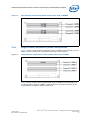
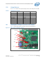
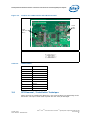
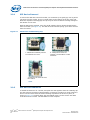
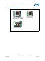
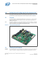
1
Intel® CoreTM 2 Duo Processor and
Intel ® Q35 Express Chipset
Development Kit
User’s Manual
October 2007
Order Number: 318476-001US
INFORMATION IN THIS DOCUMENT IS PROVIDED IN CONNECTION WITH INTEL® PRODUCTS. NO LICENSE, EXPRESS OR IMPLIED, BY ESTOPPEL OR
OTHERWISE, TO ANY INTELLECTUAL PROPERTY RIGHTS IS GRANTED BY THIS DOCUMENT. EXCEPT AS PROVIDED IN INTEL'S TERMS AND CONDITIONS
OF SALE FOR SUCH PRODUCTS, INTEL ASSUMES NO LIABILITY WHATSOEVER, AND INTEL DISCLAIMS ANY EXPRESS OR IMPLIED WARRANTY, RELATING
TO SALE AND/OR USE OF INTEL PRODUCTS INCLUDING LIABILITY OR WARRANTIES RELATING TO FITNESS FOR A PARTICULAR PURPOSE,
MERCHANTABILITY, OR INFRINGEMENT OF ANY PATENT, COPYRIGHT OR OTHER INTELLECTUAL PROPERTY RIGHT. Intel products are not intended for
use in medical, life saving, life sustaining, critical control or safety systems, or in nuclear facility applications.
Leg al Li nes and Dis clai mers
Intel may make changes to specifications and product descriptions at any time, without notice.
Intel Corporation may have patents or pending patent applications, trademarks, copyrights, or other intellectual property rights that relate to the
presented subject matter. The furnishing of documents and other materials and information does not provide any license, express or implied, by estoppel
or otherwise, to any such patents, trademarks, copyrights, or other intellectual property rights.
Designers must not rely on the absence or characteristics of any features or instructions marked “reserved” or “undefined.” Intel reserves these for
future definition and shall have no responsibility whatsoever for conflicts or incompatibilities arising from future changes to them.
Intel processor numbers are not a measure of performance. Processor numbers differentiate features within each processor family, not across different
processor families. See http://www.intel.com/products/processor_number for details.
The Intel® CoreTM 2 Duo Processor and Intel ® Q35 Express Chipset Development Kit may contain design defects or errors known as errata which may
cause the product to deviate from published specifications. Current characterized errata are available on request.
Hyper-Threading Technology requires a computer system with an Intel® Pentium® 4 processor supporting HT Technology and a HT Technology enabled
chipset, BIOS and operating system. Performance will vary depending on the specific hardware and software you use. See http://www.intel.com/
products/ht/Hyperthreading_more.htm for additional information.
Contact your local Intel sales office or your distributor to obtain the latest specifications and before placing your product order.
Copies of documents which have an order number and are referenced in this document, or other Intel literature may be obtained by calling
1-800-548-4725 or by visiting Intel's website at http://www.intel.com.
BunnyPeople, Celeron, Celeron Inside, Centrino, Centrino logo, Core Inside, FlashFile, i960, InstantIP, Intel, Intel logo, Intel386, Intel486, Intel740,
IntelDX2, IntelDX4, IntelSX2, Intel Core, Intel Inside, Intel Inside logo, Intel. Leap ahead., Intel. Leap ahead. logo, Intel NetBurst, Intel NetMerge, Intel
NetStructure, Intel SingleDriver, Intel SpeedStep, Intel StrataFlash, Intel Viiv, Intel vPro, Intel XScale, IPLink, Itanium, Itanium Inside, MCS, MMX,
Oplus, OverDrive, PDCharm, Pentium, Pentium Inside, skoool, Sound Mark, The Journey Inside, VTune, Xeon, and Xeon Inside are trademarks or
registered trademarks of Intel Corporation or its subsidiaries in the United States and other countries.
*Other names and brands may be claimed as the property of others.
Copyright © 2007, Intel Corporation. All Rights Reserved.
Intel® CoreTM 2 Duo Processor and Intel
User’s Manual
2
®
Q35 Express Chipset Development Kit
October 2007
Order Number: 318476-001US
Contents—Intel Core 2 Duo Processor and Intel Q35 Express Chipset
Contents
1.0
About This Manual ..................................................................................................... 6
1.1
Content Overview................................................................................................ 6
1.2
Text Conventions ................................................................................................ 6
1.3
Glossary of Terms and Acronyms...........................................................................7
1.4
Support Options .................................................................................................. 8
1.4.1 Electronic Support Systems ....................................................................... 8
1.4.2 Additional Technical Support ......................................................................8
1.5
Product Literature ............................................................................................... 8
2.0
Development Kit Hardware Features ....................................................................... 10
2.1
Intel® Q35 Express Chipset Development Kit Overview .......................................... 10
2.2
System Block Diagram ....................................................................................... 11
2.3
Development Kit Inventory Checklists .................................................................. 12
2.4
Processor Support ............................................................................................. 14
2.5
System Memory ................................................................................................ 14
2.5.1 Dual Channel (Interleaved) Mode Configurations ........................................ 15
2.5.2 Single Channel (Asymmetric) Mode Configurations...................................... 17
2.6
Back-Panel Connectors....................................................................................... 18
2.6.1 Audio-Connectors ................................................................................... 18
2.6.2 RJ-45 LAN Connector with Integrated LEDs ................................................ 19
2.6.3 USB Port ............................................................................................... 19
2.6.4 Coaxial S/PDIF In/Out Connector.............................................................. 19
2.6.5 eSATA Port ............................................................................................ 19
2.7
Debug Features................................................................................................. 20
2.7.1 Extended Debug Probe (XDP)................................................................... 20
2.7.2 Power LEDs ........................................................................................... 20
2.7.3 Port 80 POST Code LEDs ......................................................................... 20
2.7.4 Voltage Reference .................................................................................. 21
2.8
Development Kit Major Connectors and Jumpers.................................................... 21
2.8.1 Jumper Functions ................................................................................... 22
2.8.2 USB 2.0 Front Panel ............................................................................... 22
2.8.3 1394a Header ........................................................................................ 22
2.9
SPI Removal / Installation Technique ................................................................... 23
2.9.1 SPI Device Removal................................................................................ 24
2.9.2 SPI Device Installation ............................................................................ 24
3.0
Setting Up and Configuring the Development Kit ..................................................... 26
3.1
Overview ......................................................................................................... 26
3.2
Installing Board Standoffs .................................................................................. 26
3.3
BTX Heatsink Setup with SRM ............................................................................. 28
3.3.1 SRM Alignment on any BTX Board ............................................................ 28
3.4
Board Setup and Configuration before Boot........................................................... 30
3.5
Post Codes Definitions........................................................................................ 32
3.5.1 Normal Post Codes ................................................................................. 32
Figures
1
2
3
4
5
Board Features ........................................................................................................ 11
Intel® Q35 Express Chipset Development Kit block diagram .......................................... 12
Memory Channel and DIMM Configuration ................................................................... 15
Dual Channel (Interleaved) Mode Configuration with 2x DIMMs ...................................... 16
Dual Channel (Interleaved) Mode Configuration with 3x DIMMs ...................................... 16
October 2007
Order Number: 318476-001US
Intel® CoreTM 2 Duo Processor and Intel
®
Q35 Express Chipset Development Kit
User’s Manual
3
Intel Core 2 Duo Processor and Intel Q35 Express Chipset—Contents
6
7
8
9
10
11
12
13
14
15
16
17
18
19
20
21
22
23
24
Dual Channel (Interleaved) Mode Configuration with 4x DIMMs.......................................17
Single Channel (Asymmetric) Mode Configuration with 1x DIMM .....................................17
Single Channel (Asymmetric) Mode Configuration with 3x DIMMs ....................................18
Back-panel Connectors..............................................................................................18
LAN Connector LED locations......................................................................................19
ITP-XDP Connector location (J2BC) .............................................................................20
Major Jumper and Header Locations ............................................................................21
Location for 1394a Header and USB Front Panel ...........................................................23
SPI Socket with Retaining Clip....................................................................................24
SPI Device Installation ..............................................................................................25
Intel® Q35 Development Kits ....................................................................................26
Mounting Hole Locations ............................................................................................27
Mounting the Standoff for BTX Heatsink.......................................................................28
Casing with “Support and Retention Module” ................................................................28
BTX board alignment on SRM .....................................................................................29
Heatsink Alignment...................................................................................................29
Tightening Heatsink on the SRM and Board ..................................................................30
CPU Fan location ......................................................................................................31
2x12 Standard power supply and 2x2 power supply ......................................................32
Tables
1
2
3
4
5
6
7
8
9
10
11
12
Definition ................................................................................................................. 7
Intel Literature Centers .............................................................................................. 9
Development Kit Hardware Items ...............................................................................12
Development Kit Board Specification ...........................................................................13
Internal I/O headers .................................................................................................13
Supported Intel Technologies .....................................................................................13
Additional Features ...................................................................................................14
LAN Connector LED status .........................................................................................19
Voltage Reference detail ............................................................................................21
Intel® CoreTM 2 Duo Processor and Intel ® Q35 Express Chipset Development Kit Board
Jumpers Description .................................................................................................22
USB Front Panel .......................................................................................................22
1394a Header ..........................................................................................................23
Intel® CoreTM 2 Duo Processor and Intel
User’s Manual
4
®
Q35 Express Chipset Development Kit
October 2007
Order Number: 318476-001US
Revision History—Intel Core 2 Duo Processor and Intel Q35 Express Chipset
Revision History
Date
Revision
Description
October 2007
001
Initial release
October 2007
Order Number: 318476-001US
Intel® CoreTM 2 Duo Processor and Intel
®
Q35 Express Chipset Development Kit
User’s Manual
5
Intel Core 2 Duo Processor and Intel Q35 Express Chipset—About This Manual
1.0
About This Manual
This user’s manual describes the use of the Intel® Q35 Express Chipset Development
Kit. This manual has been written for OEMs, system evaluators, and embedded system
developers. All jumpers, headers, LED functions, and their locations on the board,
along with subsystem features and POST codes, are defined in this document.
For the latest information about the Intel® Q35 Express Chipset Development Kit
reference platform, visit:
http://developer.intel.com/design/intarch/devkits/
index.htm?iid=embed_body+devkits
For design documents related to this platform, such as schematics and layout, please
contact your Intel Representative.
1.1
Content Overview
Chapter 1.0, “About This Manual”
This chapter contains a description of conventions used in this manual. The last few
sections explain how to obtain literature and contact customer support.
Chapter 2.0, “Development Kit Hardware Features”
This chapter provides information on the development kit features and the board
capability. This includes the information on board component features, jumper settings,
pin-out information for connectors and overall development kit board capability.
Chapter 3.0, “Setting Up and Configuring the Development Kit”
This chapter provides instructions on how to configure the evaluation board and
processor assembly by setting BTX heatsink, jumpers, connecting peripherals,
providing power, and configuring the BIOS.
1.2
Text Conventions
The following notations may be used throughout this manual.
#
The pound symbol (#) appended to a signal name indicates that
the signal is active low.
Variables
Variables are shown in italics. Variables must be replaced with
correct values.
Instructions
Instruction mnemonics are shown in uppercase. When you are
programming, instructions are not case-sensitive. You may use
either upper-case or lower-case.
Numbers
Hexadecimal numbers are represented by a string of
hexadecimal digits followed by the character H. A zero prefix is
added to numbers that begin with A through F. (For example, FF
Intel® CoreTM 2 Duo Processor and Intel
User’s Manual
6
®
Q35 Express Chipset Development Kit
October 2007
Order Number: 318476001US
About This Manual—Intel Core 2 Duo Processor and Intel Q35 Express Chipset
is shown as 0FFH.) Decimal and binary numbers are
represented by their customary notations (That is, 255 is a
decimal number and 1111 1111 is a binary number). In some
cases, the letter B is added for clarity.
Units of Measure
Signal Names
1.3
The following abbreviations are used to represent units of
measure:
GByte
gigabytes
KByte
kilobytes
MByte
megabytes
MHz
megahertz
W
watts
V
volts
Signal names are shown in uppercase. When several signals
share a common name, an individual signal is represented by
the signal name followed by a number, while the group is
represented by the signal name followed by a variable (n). For
example, the lower chip-select signals are named CS0#, CS1#,
CS2#, and so on; they are collectively called CSn#. A pound
symbol (#) appended to a signal name identifies an active-low
signal. Port pins are represented by the port abbreviation, a
period, and the pin number (e.g., P1.0).
Glossary of Terms and Acronyms
This section defines conventions and terminology used throughout this document.
Table 1.
Definition (Sheet 1 of 2)
Term
Description
2nd
ADD2 Card
Generation. This card provides digital display options
Advanced Digital Display Card –
for an Intel Graphics Controller that supports ADD2+ cards. It plugs into a x16 PCI
Express* connector but uses the multiplexed SDVO interface. The card adds Video In
capabilities to platform. This Advanced Digital Display Card will not work with an Intel
Graphics Controller that supports DVO and ADD cards. It will function as an ADD2 card in
an ADD2 supported system, but video in capabilities will not work.
ACPI
Advanced Configuration and Power Interface
Core
The internal base logic in the (G)MCH
DDR2
A second generation Double Data Rate SDRAM memory technology
DMI
(G)MCH-IntelÆ ICH9 Direct Media Interface
DVI
Digital Video Interface. Specification that defines the connector and interface for digital
displays.
FSB
Front Side Bus. FSB is synonymous with Host or processor bus
GMA 3100
Intel® Graphic Media Accelerator 3100
IntelÆ ICH9
Eighth generation I/O Controller Hub component that contains additional functionality
compared to previous ICHs. The I/O Controller Hub component contains the primary PCI
interface, LPC interface, USB2, ATA-100, and other I/O functions. It communicates with
the (G)MCH over a proprietary interconnect called DMI.
IGD
Internal Graphics Device.
LVDS
Low Voltage Differential Signaling. A high speed, low power data transmission standard
used for display connections to LCD panels.
October 2007
Order Number: 318476001US
Intel® CoreTM 2 Duo Processor and Intel
®
Q35 Express Chipset Development Kit
User’s Manual
7
Intel Core 2 Duo Processor and Intel Q35 Express Chipset—About This Manual
Table 1.
Definition (Sheet 2 of 2)
Term
Description
nd
ADD2 Card
Advanced Digital Display Card – 2 Generation. This card provides digital display options
for an Intel Graphics Controller that supports ADD2+ cards. It plugs into a x16 PCI
Express* connector but uses the multiplexed SDVO interface. The card adds Video In
capabilities to platform. This Advanced Digital Display Card will not work with an Intel
Graphics Controller that supports DVO and ADD cards. It will function as an ADD2 card in
an ADD2 supported system, but video in capabilities will not work.
MCH
Memory Controller Hub component that contains the processor interface, DRAM
controller, and x16 PCI Express* port (typically, the external graphics interface). It
communicates with the I/O controller hub (Intel ICH9) and other I/O controller hubs over
the DMI interconnect. In this document MCH refers to the Intel® Q35 MCH component.
MEC
Media Expansion Card, also known as ADD2+ card. Refer to ADD2+ term for description.
PCI Express*
Third Generation input/output graphics attach called PCI Express* Graphics. PCI Express*
is a high-speed serial interface whose configuration is software compatible with the
existing PCI specifications. The specific PCI Express* implementation intended for
connecting the (G)MCH to an external Graphics Controller is a x16 link and replaces AGP.
Primary PCI
The Primary PCI is the physical PCI bus that is driven directly by the ICH9 component.
Communication between Primary PCI and the (G)MCH occurs over DMI. Note that the
Primary PCI bus is not PCI Bus 0 from a configuration standpoint.
SDVO
Serial Digital Video Out (SDVO). SDVO is a digital display channel that serially transmits
digital display data to an external SDVO device. The SDVO device accepts this serialized
format and then translates the data into the appropriate display format (i.e., TMDS,
LVDS, TV-Out). This interface is not electrically compatible with the previous digital
display channel - DVO. For the 82Q965 GMCH, it will be multiplexed on a portion of the
x16 graphics PCI Express* interface.
SDVO Device
Third party codec that uses SDVO as an input. May have a variety of output formats,
including DVI, LVDS, HDMI, TV-out, etc.
SMI
System Management Interrupt. SMI is used to indicate any of several system conditions
(such as, thermal sensor events, throttling activated, access to System Management
RAM, chassis open, or other system state related activity).
Rank
A unit of DRAM corresponding to eight x8 SDRAM devices in parallel or four x16 SDRAM
devices in parallel, ignoring ECC. These devices are usually, but not always, mounted on a
single side of a DIMM.
1.4
Support Options
1.4.1
Electronic Support Systems
Intel’s site on the World Wide Web (http://www.intel.com/) provides up-to-date
technical information and product support. This information is available 24 hours per
day, 7 days per week, providing technical information whenever you need it.
Product documentation is provided online in a variety of web-friendly formats at:
(http://developer.intel.com/)
1.4.2
Additional Technical Support
If you require additional technical support, please contact your field sales
representative or local distributor.
1.5
Product Literature
Product literature can be ordered from the following Intel literature centers:
Intel® CoreTM 2 Duo Processor and Intel
User’s Manual
8
®
Q35 Express Chipset Development Kit
October 2007
Order Number: 318476001US
About This Manual—Intel Core 2 Duo Processor and Intel Q35 Express Chipset
Table 2.
Intel Literature Centers
Location
Telephone Number
U.S. and Canada
1-800-548-4725
U.S. (from overseas)
708-296-9333
Europe (U.K.)
44(0)1793-431155
Germany
44(0)1793-421333
France
44(0)1793-421777
Japan (fax only)
81(0)120-47-88-32
October 2007
Order Number: 318476001US
Intel® CoreTM 2 Duo Processor and Intel
®
Q35 Express Chipset Development Kit
User’s Manual
9
Intel Core 2 Duo Processor and Intel Q35 Express Chipset—Development Kit Hardware Features
2.0
Development Kit Hardware Features
This chapter describes the features of the Intel® Q35 Development Kit. These
recommendations would largely apply to other designs incorporating Intel® Q35
chipset. This documentation should be used in conjunction with the datasheets,
specification updates and platform design guides for the Intel® I/O Controller Hub 9
(ICH9) Family and the Intel® Q35 Express Chipset. Contact your Intel representative
for the availability of these documents.
2.1
Intel® Q35 Express Chipset Development Kit Overview
Figure 1 shows overview of the major features present on the development kit board.
Refer to next page for system block diagram of the development kit’s motherboard.
Intel® CoreTM 2 Duo Processor and Intel
User’s Manual
10
®
Q35 Express Chipset Development Kit
October 2007
Order Number: 318476001US
Development Kit Hardware Features—Intel Core 2 Duo Processor and Intel Q35 Express Chipset
Figure 1.
Board Features
Reset button
PCI Slot
PCI Express
x1 Slot
Power Button
SPI EEPROM
(Secondary)
Port 80 LED Display
SPI EEPROM
(Primary)
PCI Express
x16 Graphics
Slot
LGA775 Processor
Socket
Intel® I/O
Controller Hub
(ICH)
SATA Port
Intel® Q35 Memory
Controller Hub (MCH)
2x2 Standard
Power Supply
2x12
Standard
Power Supply
2-DIMM per channel DDR2
667/800 (Channel-B)
2.2
2-DIMM per channel DDR2
667/800 (Channel-A)
System Block Diagram
This section will document the common features that are applicable to the Intel®
CoreTM 2 Duo Processor and Intel ® Q35 Express Chipset Development Kit. Figure 2
shows a simple block diagram of the development kit.
October 2007
Order Number: 318476001US
Intel® CoreTM 2 Duo Processor and Intel
®
Q35 Express Chipset Development Kit
User’s Manual
11
Intel Core 2 Duo Processor and Intel Q35 Express Chipset—Development Kit Hardware Features
Figure 2.
Intel® Q35 Express Chipset Development Kit block diagram
2.3
Development Kit Inventory Checklists
This section describes major hardware items which should be available on this
development kit.
Table 3.
Development Kit Hardware Items
1x 4-Layer Micro-BTX form factor (targeted dimensions: 10.5” x 10.4”) motherboard
1x Intel® CoreTM 2 Duo E6400 Processors in the LGA775 Socket
2x 1 GBytes DDR2 800 DIMM
1x BTX Heatsink with fan
1x CD-ROM contain chipset drivers (this include Intel® GMA3100 driver)
8x hex standoffs and 4x screws for bench top usage
Intel® CoreTM 2 Duo Processor and Intel
User’s Manual
12
®
Q35 Express Chipset Development Kit
October 2007
Order Number: 318476001US
Development Kit Hardware Features—Intel Core 2 Duo Processor and Intel Q35 Express Chipset
Table 4.
Development Kit Board Specification
1 PCI Express x16, 2 PCIe x1, 1 PCI expansion slots
1394a
•
1 front panel headers for support of 1 port
•
1 back panel port
Universal Serial Bus 2.0
•
2 front panel headers for support of 4 ports
•
1 internal header for support of 2 ports
•
6 back panel ports
6 SATA 3 Gb/sec ports (1 port used for eSATA)
Table 5.
Internal I/O headers
2x5 Front Panel I/O header
2x7 Front Panel audio header
1x2 Chassis intrusion header
3 four-wire fan headers
2x8 High Definition audio header
Table 6.
Supported Intel Technologies (Sheet 1 of 2)
Technology
Features/support
•
Intel® Active Management
Technology with System
Defense feature (Intel®
ICH8 DO only)
•
•
Intel® Graphics Media
Accelerator 3000
•
•
October 2007
Order Number: 318476001US
Reference Documentation
Enables remote, down-the-wire management
of out-of-band networked systems regardless
of system state, helping improve efficiency,
asset management and system security and
availability.
System Defense Feature can help block
incoming software attacks, isolate a device
from the network if infected, and proactively
alert embedded system vendors if critical
software agents are missing.
http://www.intel.com/technology/
platform-technology/intel-amt/
Dual independent display expands viewable
workspace for devices such as point-of-sale
terminals with two monitors.
Provides next-generation graphics
performance for advanced embedded
operating systems.
Delivers richer visual color and picture clarity
without the need for additional discrete
graphics cards.
http://www.intel.com/products/chipsets/
gma3000/demo/demo.html
Intel® CoreTM 2 Duo Processor and Intel
®
Q35 Express Chipset Development Kit
User’s Manual
13
Intel Core 2 Duo Processor and Intel Q35 Express Chipset—Development Kit Hardware Features
Table 6.
Supported Intel Technologies (Sheet 2 of 2)
Technology
Features/support
•
Intel® Fast Memory Access
Intel® Matrix Storage
Technology (Intel® ICH8
DO only)
•
•
Intel® High Definition Audio
Table 7.
•
Reference Documentation
Helps improve system performance by
optimizing use of available memory
bandwidth and reducing latency of memory
access by monitoring all pending read/write
requests; allows safe and efficient
overlapping of commands on all system bus
interfaces.
http://www.intel.com/products/chipsets/
q965_q963/demo/demo.html
With a second hard drive added, provides
quicker access to digital photo, video and
data files with RAID 0, 5 and 10, and greater
data protection against a hard disk drive
failure with RAID 1, 5 and 10.
http://www.intel.com/design/chipsets/
matrixstorage_sb.htm
Enables premium digital sound and delivers
advanced features such as multiple audio
streams and jack re-tasking.
Support for microphone array enables
enhanced voice capture for high-quality input
to voice-driven activities.
http://www.intel.com/design/chipsets/
hdaudio.htm
Additional Features
6 Analog audio connectors and 2 digital audio connectors
Piezo speaker for BIOS POST codes
BIOS configuration jumper
Clear CMOS jumper
Power Button
Reset Button
XDP connector
2.4
Processor Support
The Intel® Q35 Development Kit supports the following processors in the LGA775
Socket with FSB of 800/1067/1333 MHz.
These processors, with long-life support are also supported by this development kit:
• Intel® CoreTM 2 Duo E6400 (Included in the development kit)
• Intel® CoreTM 2 Duo E4300
• Intel® Pentium® Dual-Core Processor E2160
• Intel® Celeron® 440
Refer to this link for other processors which is also supported by Intel® Q35 Express
Chipset.
http://developer.intel.com/products/chipsets/Q35_Q33/index.htm
2.5
System Memory
The Intel® Q35 Express Chipset supports two types of memory organization. These are
interleaved mode and asymmetric mode. The Q35 supports:
Listed here are the summary of the system memory supported.
Intel® CoreTM 2 Duo Processor and Intel
User’s Manual
14
®
Q35 Express Chipset Development Kit
October 2007
Order Number: 318476001US
Development Kit Hardware Features—Intel Core 2 Duo Processor and Intel Q35 Express Chipset
• Non-ECC DDR2 (667/800)
• 512Mb, 1Gb and 2Gb technology
• 4 DIMMs, 4GB maximum per channel, 8GB total memory
• Dual channel (Interleaved) mode. This mode offers the highest throughput for real
world applications. Dual channel mode is enabled when the installed memory
capacities of both DIMM channels are equal. Technology and device width can vary
from one channel to the other but the installed memory capacity for each channel
must be equal. If different speed DIMMs is used between channels, the slowest
memory timing will be used.
• Single channel (Asymmetric) mode. This mode is equivalent to single channel
bandwidth operation for real world applications. This mode is used when only a
single DIMM is installed or the memory capacities are unequal. Technology and
device width can vary from one channel to the other. If different speed DIMMs is
used between channels, the slowest memory timing will be used.
Figure 3 illustrates the memory channel and DIMM configuration.
Figure 3.
Memory Channel and DIMM Configuration
Channel A DIMM 0
Channel A DIMM 1
Channel B DIMM 0
Channel B DIMM 1
2.5.1
Dual Channel (Interleaved) Mode Configurations
Figure 4 shows a dual channel configuration using two DIMMs. In this example, the
DIMM 0 sockets of both channels are populated with identical DIMMs.
October 2007
Order Number: 318476001US
Intel® CoreTM 2 Duo Processor and Intel
®
Q35 Express Chipset Development Kit
User’s Manual
15
Intel Core 2 Duo Processor and Intel Q35 Express Chipset—Development Kit Hardware Features
Figure 4.
Dual Channel (Interleaved) Mode Configuration with 2x DIMMs
Figure 5 shows a dual channel configuration using 3 DIMMs. In this example, the
combined capacity of the two DIMMs in Channel A equal the capacity of the single
DIMM in the DIMM 0 socket of Channel B.
Figure 5.
Dual Channel (Interleaved) Mode Configuration with 3x DIMMs
Figure 6 shows a dual channel configuration using 4 DIMMs. In this example, the
combined capacity of the 2x DIMMs in Channel A equals the combined capacity of the
2x DIMMs in Channel B. Also, the DIMMs are matched between DIMM 0 and DIMM 1 of
both channels.
Intel® CoreTM 2 Duo Processor and Intel
User’s Manual
16
®
Q35 Express Chipset Development Kit
October 2007
Order Number: 318476001US
Development Kit Hardware Features—Intel Core 2 Duo Processor and Intel Q35 Express Chipset
Figure 6.
Dual Channel (Interleaved) Mode Configuration with 4x DIMMs
2.5.2
Single Channel (Asymmetric) Mode Configurations
Figure 7 shows a single channel configuration using 1x DIMM. In this example, only the
DIMM 0 socket of Channel A is populated. Channel B is not populated.
Figure 7.
Single Channel (Asymmetric) Mode Configuration with 1x DIMM
Figure 8 shows a single channel configuration using 3x DIMMs. In this example, the
combined capacity of the 2x DIMMs in Channel A does not equal the capacity of the
single DIMM in the DIMM 0 socket of Channel B.
October 2007
Order Number: 318476001US
Intel® CoreTM 2 Duo Processor and Intel
®
Q35 Express Chipset Development Kit
User’s Manual
17
Intel Core 2 Duo Processor and Intel Q35 Express Chipset—Development Kit Hardware Features
Figure 8.
Single Channel (Asymmetric) Mode Configuration with 3x DIMMs
2.6
Back-Panel Connectors
Figure 9 shows back-panel connectors for the development kit.
Figure 9.
Back-panel Connectors
Side
Speaker
Out
RJ-45 LAN Port
1394a Port
Line-in Jack
Rear
Speaker
Out
USB Port
(Total 6
Ports)
2.6.1
eSATA Port
VGA Analog
Display
S/PDIF IN
S/PDIF OUT
Line-out
Jack
Center/ Mic In Jack
Sub
Woofer
Speaker
Out Jack
Audio-Connectors
This development kit board supports up to 7.1-channel audio configuration. It is
backward compatible with 5.1, 2.1 and stereo (2-channel) audio configuration as well.
Line In Jack (Light Blue)
This audio jack is used to for line in devices, including some optical devices.
Line Out Jack (Light Green)
This audio jack is used for line out devices. It’s used in 2.1, 5.1 and 7.1 channel- audio
configuration. It can be used for headphone and stereo speaker as well.
Mic In Jack (Pink)
This audio jack is use for microphone input.
Intel® CoreTM 2 Duo Processor and Intel
User’s Manual
18
®
Q35 Express Chipset Development Kit
October 2007
Order Number: 318476001US
Development Kit Hardware Features—Intel Core 2 Duo Processor and Intel Q35 Express Chipset
Center/Subwoofer Speaker Out Jack (Orange)
This audio jack is used to connect to center/subwoofer speakers in a 5.1 and 7.1channel audio configuration.
Rear Speaker Out (Black)
This audio jack is used to connect to rear speakers in a 5.1 and 7.1-channel audio
configuration.
Side Speaker Out (Gray)
This audio jack is used to connect to side speakers for 7.1-channel audio configuration
only.
2.6.2
RJ-45 LAN Connector with Integrated LEDs
Two LEDs are built into the RJ-45 LAN connector (as shown in Figure 10). Table 8
describes the LED states when the board is powered up and the Gigabit LAN subsystem
is operating.
Figure 10.
LAN Connector LED locations
Table 8.
LAN Connector LED status
LED
Left
Right
2.6.3
Color
Green
LED State
Condition
Off
LAN link is not established
On
LAN link is established
Blinking
LAN activity is occurring
N/A
Off
10 Mbits/sec data rate is selected
Green
On
100 Mbits/sec data rate is selected
Yellow
On
1000 Mbits/sec data rate is selected
USB Port
The USB port supports the USB 1.1/2.0 specification.
2.6.4
Coaxial S/PDIF In/Out Connector
This connector provides digital audio input and output from external audio system that
supports digital coaxial audio. Ensure that the audio system provides a coaxial digitalin/out connector.
2.6.5
eSATA Port
This development kits support the first generation eSATA port.
October 2007
Order Number: 318476001US
Intel® CoreTM 2 Duo Processor and Intel
®
Q35 Express Chipset Development Kit
User’s Manual
19
Intel Core 2 Duo Processor and Intel Q35 Express Chipset—Development Kit Hardware Features
2.7
Debug Features
2.7.1
Extended Debug Probe (XDP)
The reference board provides a JTAG-compliant test access port (TAP) for attachment
of an XDP connector. The XDP connector and associated circuitry enable the use of the
ITP for the particular processor to interrupt the boot sequence and view processor
status.
The XDP connector is located on the backside of the board at location J2BC. Refer to
Figure 11 to the XDP connector location. Take notes that ITP-XDP SSA connector is
needed. Refer to diagram below for the ITP-XDP SSA connector.
Figure 11.
ITP-XDP Connector location (J2BC)
ITP-XDP
Connector
ITP-XDP SSA Connector is
needed in order to
connect to ITP-XDP2/3
tools
2.7.2
Power LEDs
Power LEDs on the board indicate when standby power is being applied to the standby
planes. When lit they indicate that no DIMM modules should be inserted or removed. To
install or replace DIMM modules insure that AC power to the power supply is removed
by unplugging the AC power cord from the power supply or placing the switch on the
power supply to the open position.
Caution:
Removing DIMM modules when the standby power LEDs is lit could result in damage to
the memory devices on those modules.
2.7.3
Port 80 POST Code LEDs
Two LEDs display the POST codes output from Port 80 to indicate the progress of the
boot sequence or display the POST code of the last operation successfully completed
during the boot sequence. Please refer to Section 3.4 for more information on Port 80
code reference.
Intel® CoreTM 2 Duo Processor and Intel
User’s Manual
20
®
Q35 Express Chipset Development Kit
October 2007
Order Number: 318476001US
Development Kit Hardware Features—Intel Core 2 Duo Processor and Intel Q35 Express Chipset
2.7.4
Voltage Reference
See Table 9 for details of the expected voltage levels for each voltage rail on the CRB.
Table 9.
Voltage Reference detail
Voltage Rail
2.8
Expected Voltage
Voltage Rail
Expected Voltage
VCC
5.0
V_1P25_CORE
1.25
VCC3
3.3
V_1P25_CL_MCH
1.25
+12V
12
V_1P25_PCIEXPRESS
1.25
-12V
-12
V_SM
1.8
V_5P0_STBY\G
5.0
V_SM_VTT
0.9
V_3P3_STBY\G
3.3
V_3P3_CL
3.3
V_1P5_ICH
1.5
V_3P3_PCIVAUX
3.3
V_1P05_ICH_CORE
1.05
VDD_CLK
3.3
V_FSB_VTT
1.2
VCC_CLK_IO
0.8
VCCP
Varies
Development Kit Major Connectors and Jumpers
Figure 12 shows major jumpers and headers used on the development kit.
Figure 12.
Major Jumper and Header Locations
J4LB/J10LB
J6LB
J115LB
J14LB
J15LB
J16LB
J7LB
October 2007
Order Number: 318476001US
Intel® CoreTM 2 Duo Processor and Intel
®
Q35 Express Chipset Development Kit
User’s Manual
21
Intel Core 2 Duo Processor and Intel Q35 Express Chipset—Development Kit Hardware Features
2.8.1
Jumper Functions
Table 10 provides a list of the setting definitions for the Intel® CoreTM 2 Duo Processor
and Intel ® Q35 Express Chipset Development Kit.
Table 10.
Intel® CoreTM 2 Duo Processor and Intel ® Q35 Express Chipset Development
Kit Board Jumpers Description
Jumper
Description
J6LB
Clear CMOS
(1-2: Normal, 2-3: Clear CMOS)
1-2
J115LB
RTC Reset
(1-2: Normal, 2-3: Clear)
1-2
J7LB
Config /Recovery
(1-2: Normal, 2-3: Configure, jumper removed –
recovery)
J4LB/J10LB
2.8.2
Default Position
Manufacturing mode
(enable if jumper plug-in)
1-2
Empty
USB 2.0 Front Panel
There are 4 USB 2.0 Front Panel can be found in the development kits board. Front
panel USB header thermistor protection is required. USB front panel is label as U14LB,
U15LB, U16LB and U1FW on the boards. Refer to Figure 12 for header location of
U14LB, U15LB and U16LB. Refer to Figure 13 for U1FW.
Table 11.
USB Front Panel
Pin Number
2.8.3
Definition
1
5V
2
5V
3
USB Dx-
4
USB Dy-
5
USB Dx+
6
USB Dy+
7
GND
8
GND
9
No pin
10
No connect
1394a Header
The development kit board supports a 1394a solution on the PCIe bus with a single
1394a port on the back panel (see Figure 9) and another header supporting a 1394a
port (see Figure 13). Front panel 1394a header thermistor protection is required.
Intel® CoreTM 2 Duo Processor and Intel
User’s Manual
22
®
Q35 Express Chipset Development Kit
October 2007
Order Number: 318476001US
Development Kit Hardware Features—Intel Core 2 Duo Processor and Intel Q35 Express Chipset
Figure 13.
Location for 1394a Header and USB Front Panel
J24LB
1394a
Header
U1FW
(USB Front
Panel)
Table 12.
1394a Header
Pin Number
2.9
Definition
1
NDCD A-
2
NSIN A
3
NSOUT A
4
NDTR A-
5
GND
6
NDSR A-
7
NRTS A-
8
NCTS A-
9
NRI A-
10
No Pin
SPI Removal / Installation Technique
When removing or installing the SPI device, care must be taken to avoid damage to the
SPI socket. The cap is constructed of plastic and can easily be damaged.
October 2007
Order Number: 318476001US
Intel® CoreTM 2 Duo Processor and Intel
®
Q35 Express Chipset Development Kit
User’s Manual
23
Intel Core 2 Duo Processor and Intel Q35 Express Chipset—Development Kit Hardware Features
2.9.1
SPI Device Removal
To remove the SPI device from the socket, use a tweezer tip to gently pry one leg of the
cap away from the socket. There is a small latch on the bottom of the leg of the cap.
Once the cap latch is disengaged, the cap may be removed without causing damage to
the latches on the ends.
With the SPI device exposed, move the small retaining clip to release the SPI device
from the socket (see Figure 14). The SPI device should now spring up to allow removal
from the socket.
Figure 14.
SPI Socket with Retaining Clip
1. Follow the unclench process
to unclench the cover.
2. Clamp the fresh IC at
location 1 and location 2 with
tweezers.
3. Remove the fresh IC from
the socket.
2.9.2
SPI Device Installation
To Install an SPI device in a socket, first place the side opposite from the retaining clip
into the socket at an angle of approximately 15 degrees. Continue to gently insert the
device into the socket until the metal retaining clip latches the device in place, as
shown in Figure 15. Carefully place the cap straight down over the device until both
ends latch into the socket. The installation is now complete.
Intel® CoreTM 2 Duo Processor and Intel
User’s Manual
24
®
Q35 Express Chipset Development Kit
October 2007
Order Number: 318476001US
Development Kit Hardware Features—Intel Core 2 Duo Processor and Intel Q35 Express Chipset
Figure 15.
SPI Device Installation
1. Place the fresh IC into the
socket. Match pin 1. on the IC
to pin 1 on the socket.
2. Close the cover.
3. Lock the cover with
the hook.
October 2007
Order Number: 318476001US
Intel® CoreTM 2 Duo Processor and Intel
®
Q35 Express Chipset Development Kit
User’s Manual
25
Intel Core 2 Duo Processor and Intel Q35 Express Chipset—Setting Up and Configuring the
Development Kit
3.0
Setting Up and Configuring the Development Kit
This chapter discusses basic board set up and operation. Please refer to Chapter 2.0 for
the board layout, jumper setting location and the component reference designator.
3.1
Overview
The board consists of a baseboard populated with one Intel® Core™ 2 Duo processor
E6400, the Intel® Q35 Express chipset, and other system board components and
peripheral connectors.
Note:
This board is shipped as an open system allowing for maximum flexibility in changing
hardware configuration and peripherals. Since the board is not in a protective chassis,
take extra precaution when handling and operating the system.
Figure 16.
Intel® Q35 Development Kits
3.2
Installing Board Standoffs
Caution:
The evaluation board in this development kit is shipped as an open system allowing for
maximum flexibility in changing hardware configuration and peripherals in the lab
Intel® CoreTM 2 Duo Processor and Intel
User’s Manual
26
®
Q35 Express Chipset Development Kit
October 2007
Order Number: 318476001US
Setting Up and Configuring the Development Kit—Intel Core 2 Duo Processor and Intel Q35
Express Chipset
environment. Since the board is not in a protective chassis, the user is required to
observe extra precautions when handling and operating the system.
The board is a standard uBTX form factor and provides non-plated mounting holes with
top and bottom ground rings. If the board is not going to be used in a chassis,
standoffs are included for bench top use in the lab environment.
The development kit includes eight hex standoffs and for screws to attach to the board
for bench top use. Four of the standoffs are used to mount the heatsink (refer to
Section 3.3 for heatsink installation). Attach standoffs to the screws to the board at the
following mounting hole locations.
1. Insert screw through top mounting hole for the BTX Heatsink. Refer to Figure 17 for
the mounting hole location.
2. Place standoff on backside of board and hand tighten to screw. Refer to Figure 18
for guide.
3. Repeat for additional standoffs on the board until all standoffs are installed. Refer
to Figure 17 for recommended mounting hole locations.
Figure 17.
Mounting Hole Locations
J24LB
Recommended
Mounting Hole
Locations
Mounting Hole for
BTX heatsink
Locations
October 2007
Order Number: 318476001US
Intel® CoreTM 2 Duo Processor and Intel
®
Q35 Express Chipset Development Kit
User’s Manual
27
Intel Core 2 Duo Processor and Intel Q35 Express Chipset—Setting Up and Configuring the
Development Kit
Figure 18.
Mounting the Standoff for BTX Heatsink
3.3
BTX Heatsink Setup with SRM
This section describes BTX casing which uses “Support and Retention Module (SRM)” as
shown in Figure 19.
Note:
SRM is not included in this development kits.
Figure 19.
Casing with “Support and Retention Module”
3.3.1
SRM Alignment on any BTX Board
Attach the BTX Thermal Module Assembly (TMA) over the processor to the Support and
Retention Module (SRM) by following procedures described below.
Intel® CoreTM 2 Duo Processor and Intel
User’s Manual
28
®
Q35 Express Chipset Development Kit
October 2007
Order Number: 318476001US
Setting Up and Configuring the Development Kit—Intel Core 2 Duo Processor and Intel Q35
Express Chipset
1. Place the uBTX board on the Support and Retention Module (SRM) so that the holes
A, B, C and D on the PCB line up with the corresponding locations on the SRM (see
Figure 19). The board and SRM assembly should look like Figure 20.
Figure 20.
BTX board alignment on SRM
2. Place the heatsink on top of the processor. The heatsink should align with the holes
on the SRM and board as shown below Figure 21. Clean the surface of the
processor with isopropyl alcohol before attaching the heatsink.
Figure 21.
Heatsink Alignment
3. Use two 6-32 screws to partially tighten the rear end of the heatsink to the board
and the SRM as shown in Figure 22. The screw uses the threaded holes of the SRM
for retention.
October 2007
Order Number: 318476001US
Intel® CoreTM 2 Duo Processor and Intel
®
Q35 Express Chipset Development Kit
User’s Manual
29
Intel Core 2 Duo Processor and Intel Q35 Express Chipset—Setting Up and Configuring the
Development Kit
Figure 22.
Tightening Heatsink on the SRM and Board
3.4
Board Setup and Configuration before Boot
Follow the steps below to operate the board.
Warning:
Before starting, ensure the power supply is not connected to the board.
Ensure a safe and static-free work environment before removing any components from
their anti-static packaging. The Development Platform is susceptible to electrostatic
discharge, which may cause failure or unpredictable operation.
The Development Platform must be operated on a flame retardant surface because a
chassis is not included with the platform.
Caution:
Connecting the wrong cable or reversing a cable may damage the board and may
damage the device being connected. Since the board is not in a protective chassis, use
caution when connecting cables to the board.
Caution:
The power supply cord is the main disconnect device to main power (AC power). The
socket outlet should be installed near the equipment and should be readily accessible.
To avoid shock, ensure that the power cord is connected to a properly wired and
grounded receptacle. Do not connect/disconnect any cables or perform installation/
maintenance of the boards in this product during an electrical storm. Ensure that any
equipment to which this product will be attached is also connected to properly wired
and grounded receptacles.
Note:
Ensure that setting up the ATX power supply is the final step performed in the process
of assembly.
1. Physically inspect the motherboard for obvious defects. Note that each reference
board has been tested prior to distribution, but a visual check should be performed
to ensure no damage has occurred during shipping.
Intel® CoreTM 2 Duo Processor and Intel
User’s Manual
30
®
Q35 Express Chipset Development Kit
October 2007
Order Number: 318476001US
Setting Up and Configuring the Development Kit—Intel Core 2 Duo Processor and Intel Q35
Express Chipset
2. Set jumpers to default positions. Refer to Section 2.8.1 for default positions.
3. Install the processor and ensure the 4-pin CPU fan power connector is installed on
header shown in Figure 23.
Figure 23.
CPU Fan location
4-pin CPU Fan Power
4. Install the DDR2 DIMM in the Channel A Slot 0 connector. DIMMs should never be
inserted or removed unless the power supply is disconnected from the AC power
source. Refer to Section 2.5 for system memory configuration.
5. Connect a SATA hard drive, USB keyboard, USB mouse, and VGA monitor (video
card is optional).
6. Connect a 2x12 standard power supply and 2x2 standard power supply as well.
Refer to Figure 24 for the location.
7. Plug the power cable into the back of the power supply, leaving the switch in the
OFF position.
8. Once the board is set up, plug the cord into the power source. Switch on the power
supply.
9. Press the power button. Refer to Figure 24 or Figure 1 for power-on button
location.
October 2007
Order Number: 318476001US
Intel® CoreTM 2 Duo Processor and Intel
®
Q35 Express Chipset Development Kit
User’s Manual
31
Intel Core 2 Duo Processor and Intel Q35 Express Chipset—Setting Up and Configuring the
Development Kit
Figure 24.
2x12 Standard power supply and 2x2 power supply
Power-on button
2x12 Standard
power supply
2x2 Standard
power supply
3.5
Post Codes Definitions
The CRB BIOS writes progress and error codes to Port 80 during POST. These codes are
defined below.
3.5.1
Normal Post Codes
Uncompressed INIT code checkpoints
Before D1 – Early chipset and SIO initialization. NMI disabled.
D1
Perform keyboard controller BAT test. Save power-on CPUID to
scratch CMOS.
D0
Go to flat mode with 4GB limit. Start checksum verification.
D2
Disable cache and begin sizing full memory array.
D3
Additional chipset initialization, re-enable cache.
D4
Test base 512 MB of memory, adjust policies and cache first 8
MB.
D5
Bootblock code copied from ROM to lower system memory. BIOS
now executes out of RAM.
D6
Check for recovery mode and verify main BIOS checksum.
If either in recovery mode or main BIOS checksum is bad, go to check point E0
else goto checkpoint D7.
Intel® CoreTM 2 Duo Processor and Intel
User’s Manual
32
®
Q35 Express Chipset Development Kit
October 2007
Order Number: 318476001US
Setting Up and Configuring the Development Kit—Intel Core 2 Duo Processor and Intel Q35
Express Chipset
D7
Restore CPUID value to register. Bootblock runtime module
transferred to system memory.
D8
Main BIOS runtime code is to be decompressed.
D9
Copy main BIOS into system memory.
E1-E8
OEM memory detection/configuration error. Range reserved for
chipset vendors/OEMs.
EC-EE
Boot Block Recovery Code Checkpoints
E0
Initialize Floppy Controller, DMA controller and interrupt
controller.
E9
Set up floppy controller and data. Attempt to read from floppy.
EA
Enable ATAPI hardware. Attempt to read from ARMD and ATAPI
CDROM.
EB
Disable ATAPI hardware. Jump back to checkpoint E9.
EF
Read error occurred on media. Jump back to checkpoint EB.
EF
Floppy read error.
F0
Search for pre-defined recovery file in root directory.
F1
Recovery file not found.
F2
Start reading FAT table and analyze FAT to find the clusters
occupied by the recovery file.
F3
Start reading recovery file cluster by cluster.
F5
Disable L1 cache.
FA
Check validity of recovery file configuration against
configuration of FLASH part.
FB
Enable FLASH write through POEM and chipset specific method.
Detect FLASH type.
F4
Recovery file size does not match FLASH part size.
FC
Erase FLASH.
FD
Program FLASH.
FF
Flash program successful. Disable FLASH write. Restore CPUID
into register.
Runtime POST Code Checkpoints
03
Disable NMI, Parity, EGA video and DMA controllers. Initialize
BIOS, POST and runtime data area.
04
Verify CMOS checksum. Initialize status register A.
05
Initialize interrupt hardware and interrupt vector table.
06
Do R/W to CH-2 count reg. Initialize CH-0 as system timer.
Install POSTINTCH handler.
Enable IRQ0 in PIC for system timer interrupt.
October 2007
Order Number: 318476001US
Intel® CoreTM 2 Duo Processor and Intel
®
Q35 Express Chipset Development Kit
User’s Manual
33
Intel Core 2 Duo Processor and Intel Q35 Express Chipset—Setting Up and Configuring the
Development Kit
08
Initialize CPU. The BAT test performed on KBC. Auto detection
of KB and MS.
C0
Early CPU Init Start. Disable cache and init local APIC.
C1
Set up boot strap processor information.
C2
Set up boot strap processor for POST.
C5
Enumerate and set up application processors.
C6
Re-enable cache for boot strap processor.
C7
Early CPU Init Exit.
0A
Initialize 8042 compatible keyboard controller.
0B
Detect PS/2 mouse.
0C
Detect keyboard in KBC port.
0E
Test and initialization of different input devices. Uncompress all
language, BIOS logo and Silent logo.
13
Early POST initialization of chipset registers.
11
Going to check pressing of <INS>, <END> key during poweron.
12
To init CMOS if “Init CMOS in every boot” is set or <END> key
is pressed. Going to disable DMA and Interrupt controllers.
13
Video display is disabled and port-B is initialized. Chipset init
about to begin.
24
Uncompress and initialize platform specific BIOS modules.
30
Initialize System Management Interrupt.
2A
Initialize different devices through Device Initialization Manager
(DIM).
2C
Detect and initialize video adapter with optional ROM.
2E
Initialize all output devices.
31
Allocate memory for ADM module. Uncompress and initialize
ADM module.
33
Initialize silent boot mode. Set window to display text
information.
37
Display sign-on message, CPU information, setup message and
OEM specific information.
38
Initialize different devices through DIM.
39
Initialize DMAC-1 and DMAC-2.
3A
Initialize RTC date/time.
3B
Test and display total memory in system.
3C
Mid POST initialization of chipset registers.
40
Detect peripheral devices.
50
Program memory hole or implementation specific adjustments
to system memory.
52
Update CMOS memory size. Allocate memory for extended BIOS
data area.
Intel® CoreTM 2 Duo Processor and Intel
User’s Manual
34
®
Q35 Express Chipset Development Kit
October 2007
Order Number: 318476001US
Setting Up and Configuring the Development Kit—Intel Core 2 Duo Processor and Intel Q35
Express Chipset
60
Initialize NUM-LOCK status and program typematic rate.
75
Initialize INT-13 and prepare for IPL detection.
78
Initialize IPL devices controlled by BIOS and option ROMs.
7A
Initialize option RMs.
7C
Generate and write contents of ESCD in NVRAM.
84
Log errors encountered during POST.
85
Display errors and prompt for user response.
87
Execute BIOS setup if requested.
8C
Late POST chipset register initialization.
8D
Build ACPI tables if supported.
8E
Program peripheral parameters. Enable/Disable NMI as
selected.
90
Late POST initialization of system management interrupt.
A0
Check for boot password.
A1
Clean-up work needed before boot to OS.
A2
Prepare runtime image for different BIOS modules. Initialize MS
IRQ Routing Table.
A4
Initialize runtime language module.
A7
Display system configuration screen. Initialize CPU for boot,
program MTRRs.
A8
Prepare CPU for boot including final MTRR values.
A9
Wait for user input at configuration display if needed.
AA
Uninstall POST INT1CH vector and INT09 vector. De-initialize
ADM module.
AB
Prepare BBS for INT19 boot.
AC
End of POST initialization of chipset registers.
B1
Save system context for ACPI.
00
Pass control to OS loader via INT19.
61-70
OEM POST error. Reserved for chipset vendors and system
manufacturers.
October 2007
Order Number: 318476001US
Intel® CoreTM 2 Duo Processor and Intel
®
Q35 Express Chipset Development Kit
User’s Manual
35
Intel Core 2 Duo Processor and Intel Q35 Express Chipset—Setting Up and Configuring the
Development Kit
Intel® CoreTM 2 Duo Processor and Intel
User’s Manual
36
®
Q35 Express Chipset Development Kit
October 2007
Order Number: 318476001US