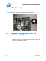
1
Intel® Core™ 2 Duo Processor
and Intel® Q45 Express Chipset
Development Kit
User’s Manual
September 2008
Revision 001
Document Number: 320632-001US
INFORMATION IN THIS DOCUMENT IS PROVIDED IN CONNECTION WITH INTEL® PRODUCTS. NO LICENSE, EXPRESS OR
IMPLIED, BY ESTOPPEL OR OTHERWISE, TO ANY INTELLECTUAL PROPERTY RIGHTS IS GRANTED BY THIS DOCUMENT. EXCEPT
AS PROVIDED IN INTEL'S TERMS AND CONDITIONS OF SALE FOR SUCH PRODUCTS, INTEL ASSUMES NO LIABILITY
WHATSOEVER, AND INTEL DISCLAIMS ANY EXPRESS OR IMPLIED WARRANTY, RELATING TO SALE AND/OR USE OF INTEL
PRODUCTS INCLUDING LIABILITY OR WARRANTIES RELATING TO FITNESS FOR A PARTICULAR PURPOSE, MERCHANTABILITY,
OR INFRINGEMENT OF ANY PATENT, COPYRIGHT OR OTHER INTELLECTUAL PROPERTY RIGHT.
UNLESS OTHERWISE AGREED IN WRITING BY INTEL, THE INTEL PRODUCTS ARE NOT DESIGNED NOR INTENDED FOR ANY
APPLICATION IN WHICH THE FAILURE OF THE INTEL PRODUCT COULD CREATE A SITUATION WHERE PERSONAL INJURY OR
DEATH MAY OCCUR.
Intel may make changes to specifications and product descriptions at any time, without notice. Designers must not rely on the
absence or characteristics of any features or instructions marked "reserved" or "undefined." Intel reserves these for future
definition and shall have no responsibility whatsoever for conflicts or incompatibilities arising from future changes to them. The
information here is subject to change without notice. Do not finalize a design with this information.
The products described in this document may contain design defects or errors known as errata which may cause the product to
deviate from published specifications. Current characterized errata are available on request.
Contact your local Intel sales office or your distributor to obtain the latest specifications and before placing your product order.
45-nm products are manufactured on a lead-free process. Lead-free per EU RoHS directive July, 2006. Some E.U. RoHS
exemptions may apply to other components used in the product package. Residual amounts of halogens are below November,
2007 proposed IPC/JEDEC J-STD-709 standards.
This device is protected by U.S. patent numbers 5,315,448 and 6,516,132, and other intellectual property rights. The use of
Macrovision's copy protection technology in the device must be authorized by Macrovision and is intended for home and other
limited pay-per-view uses only, unless otherwise authorized in writing by Macrovision. Devices incorporating Macrovision’s copy
protection technology can only be sold or distributed to companies appearing on Macrovision’s list of “Authorized Buyers” at:
www.macrovision.com. Reverse engineering or disassembly is prohibited.
Intel, Celeron, Intel Core, Intel Speedstep, and the Intel logo are trademarks of Intel Corporation in the U.S. and other
countries.
*Other names and brands may be claimed as the property of others.
Copyright © 2008, Intel Corporation. All rights reserved.
2
User’s Manual
Contents
1
Introduction .....................................................................................................7
1.1
1.2
1.3
1.4
1.5
2
Development Kits Hardware Features................................................................. 12
2.1
2.2
2.3
2.4
2.5
2.6
2.7
2.8
2.9
3
Overview ............................................................................................31
ATX Heatsink Setup ..............................................................................32
ATX Heatsink Alignment on the Intel® Q45 Development Kit Platform ......... 32
Board Setup and Configuration before Boot .............................................. 34
3.4 Post Codes Definitions ..................................................................... 35
3.5.1
Normal Post Codes .................................................................. 36
BIOS Setup Utility...........................................................................................42
4.1
User’s Manual
Intel® Q45 Development Kits Overview................................................... 12
System Block Diagram .......................................................................... 13
Development Kit Inventory Checklist....................................................... 14
Processor Support ................................................................................ 15
System Memory ...................................................................................15
2.5.1
Dual Channel (Interleaved) Mode Configurations.......................... 16
2.5.2
Single Channel (Asymmetric) Mode Configurations ....................... 18
Back-Panel Connectors.......................................................................... 19
2.6.1
Audio-Connectors .................................................................... 20
2.6.2
RJ-45 LAN Connector with Integrated LEDs ................................. 21
2.6.3
USB Port ................................................................................21
2.6.4
HDMI Port .............................................................................. 21
Debug Features....................................................................................22
2.7.1
Extended Debug Probe (XDP).................................................... 22
2.7.2
Power LEDs ............................................................................ 23
2.7.3
Port 80 POST Code LEDs .......................................................... 23
2.7.4
Voltage Reference ................................................................... 23
Development Kit’s Major Connector and Jumper........................................ 24
2.8.1
Jumper Functions ....................................................................24
2.8.2
USB 2.0 Front Panel ................................................................ 25
2.8.3
1394a Header .........................................................................26
SPI Removal / Installation Technique................................................... 28
2.9.1
SPI Device Installation ............................................................. 28
2.9.2
SPI Device Removal................................................................. 30
Setting Up and Configuring Development Kits ..................................................... 31
3.1
3.2
3.3
3.4
3.5
4
Content Overview...................................................................................7
Text Conventions ...................................................................................8
Terminology ..........................................................................................9
Support Options ...................................................................................10
1.4.1
Electronic Support Systems ...................................................... 10
1.4.2
Additional Technical Support ..................................................... 10
Product Literature ................................................................................ 11
Main...................................................................................................42
3
4.2
4.3
4.4
4.5
4.6
4.7
4.8
4.9
System Overview .................................................................... 42
4.1.1
Advance..............................................................................................43
PCIPnP ...............................................................................................48
Boot ...................................................................................................48
4.4.1
Boot Setting Configuration........................................................ 48
Security ..............................................................................................49
Chipset ............................................................................................... 50
Virtual Appliance ..................................................................................55
System Validation (SV) .........................................................................56
Exit ....................................................................................................57
Figures
Figure
Figure
Figure
Figure
Figure
Figure
Figure
Figure
Figure
Figure
Figure
Figure
Figure
Figure
Figure
Figure
Figure
Figure
Figure
Figure
Figure
Figure
Figure
Figure
Figure
Figure
Figure
Figure
4
2-1. Board Features ...............................................................................12
2-2. Intel® Q45 Development Kits Block Diagram ...................................... 13
2-3. Memory Channel and DIMM Configuration ..........................................16
2-4. Dual Channel (Interleaved) Mode Configuration with 2X DIMMs ............. 16
2-5. Dual Channel (Interleaved) Mode Configuration with 3X DIMMs ............. 17
2-6. Dual Channel (Interleaved) Mode Configuration with 4x DIMMs ............. 17
2-7. Single Channel (Asymmetric) Mode Configuration with 1X DIMM............ 18
2-8. Single Channel (Asymmetric) Mode Configuration with 3x DIMMs .......... 18
2-9. Back Panel Connectors for Development Kits ...................................... 19
2-10. LAN Connector LED Locations ......................................................... 21
2-11. ITP-XDP Connector Location (J2BC) ................................................. 22
2-12. Major Jumpers and Headers Location on the Development Kits ............ 24
2-13. USB 2.0 Front Panel ...................................................................... 25
2-14. USB 2.0 Front Panel ...................................................................... 26
2-15. Location for 1394a Header and USB Front Panel ................................ 27
2-16. Pick and Tweezer .......................................................................... 28
2-17. Doors 1 and 2 ..............................................................................28
2-18. Opening Door 1 ............................................................................29
2-19. Opening Door 2 ............................................................................29
2-20. Installing the SPI Device ................................................................29
2-21. Closing Doors 1 and 2.................................................................... 30
2-22. Removing the SPI Device ............................................................... 30
3-1. Intel® Q45 Development Kit ............................................................ 31
3-2. Intel® Q45 Development Kit Platform and the ATX Heatsink ................. 32
3-3. ATX Heatsink Alignment on the Intel® Q45 Development Kit Board ....... 33
3-4. Pressing the ATX Heatsink While Holding the Board .............................33
3-5. CPU Fan Location............................................................................ 34
3-6. 2x12 Standard Power Supply and 2x2 Power Supply ............................ 35
User’s Manual
Tables
Table
Table
Table
Table
Table
Table
Table
Table
Table
Table
Table
Table
Table
Table
Table
Table
Table
Table
Table
Table
Table
Table
Table
Table
Table
Table
Table
Table
Table
Table
Table
Table
User’s Manual
1-1. Intel Literature Centers.....................................................................11
2-1. LAN Connector LED Status ................................................................ 21
2-2. Voltage Reference Detail ...................................................................23
2-3. Intel® Q45 Development Kits CRB Board Jumpers Description ............... 24
2-4. USB Front Panel...............................................................................25
2-5. 1394a Header .................................................................................26
3-1. Boot Block Initialization Code Checkpoints ........................................... 36
3-2. Boot Block Recovery Code Check Points .............................................. 38
3-3. Runtime POST Code Checkpoints........................................................ 39
4-1. CPU Configuration ............................................................................43
4-2. IDE Configuration ............................................................................44
4-3. Floppy Configuration ........................................................................45
4-4. ACPI Configuration...........................................................................45
4-5. AHCI Configuration ..........................................................................46
4-6. Intel AMT Configuration ....................................................................46
4-7. MPS Configuration............................................................................47
4-8. SMBIOS Configuration ......................................................................47
4-9. Remote Access Configuration............................................................. 47
4-10. Trusted Computing ......................................................................... 47
4-11. USB Configuration ..........................................................................47
4-12. PCIPnP Configuration ......................................................................48
4-13. Boot Setting Configuration............................................................... 48
4-14. Boot Setting Configuration............................................................... 49
4-15. Northbridge Configuration ...............................................................50
4-16. Southbridge Configuration ...............................................................52
4-17. Intel ME Subsystem Configuration ....................................................53
4-18. PCI Express Configuration ...............................................................54
4-19. VE Subsystem Configuration ............................................................ 55
4-20. Virtual Appliance ............................................................................55
4-21. SV SMI Management ...................................................................... 56
4-22. SV SATA Management ....................................................................56
4-23. Exit ..............................................................................................57
5
Revision History
Revision
Number
001
Description
Revision Date
• Initial release.
September 2008
§
6
User’s Manual
Introduction
1
Introduction
This user’s manual describes the use of the Intel® Q45 Express Chipset Development
Kit. This manual has been written for OEMs, system evaluators, and embedded
system developers. All jumpers, headers, LED functions, and their locations on the
board, along with subsystem features and POST codes, are defined in this document.
For the latest information about the Intel® Q45 Express Chipset Development Kit
reference platform, visit:
http://developer.intel.com/design/intarch/devkits/index.htm?iid=embed_body+devkits
For design documents related to this platform, such as schematics and layout, please
contact your Intel Representative.
1.1
Content Overview
Chapter 1, “About This Manual” – This chapter contains a description of conventions
used in this manual. The last few sections explain how to obtain literature and contact
customer support.
Chapter 2, “Development Kits Hardware Features” – This chapter provides information
on the development kit features and the board capability. This includes the
information on board component features, jumper settings, pin-out information for
connectors and overall development kit board capability.
Chapter 3, “Development Kits Board ” – This chapter provides instructions on how to
configure the evaluation board and processor assembly by setting ATX heatsink,
jumpers, connecting peripherals, providing power, and configuring the BIOS.
Chapter 4, “BIOS Setup Utility” – This chapter provides the BIOS function and how to
configure the BIOS features. This includes the BIOS option tab functions like the Main
System Overview, Advance, PCIPnP, Boot, Security, Chipset, SV, and Exit.
User’s Manual
7
Introduction
1.2
Text Conventions
The following notations may be used throughout this manual.
#
The pound symbol (#) appended to a signal name indicates that
the signal is active low.
Variables
Variables are shown in italics. Variables must be replaced with
correct values.
Instructions
Instruction mnemonics are shown in uppercase. When you are
programming, instructions are not case-sensitive. You may use
either uppercase or lowercase.
Numbers
Hexadecimal numbers are represented by a string of hexadecimal
digits followed by the character H. A zero prefix is added to
numbers that begin with A through F. (For example, FF is shown
as 0FFH.) Decimal and binary numbers are represented by their
customary notations. (That is, 255 is a decimal number and 1111
1111 is a binary number.) In some cases, the letter B is added for
clarity.
Units of Measure
The following abbreviations are used to represent units of
measure:
Signal Names
8
GByte
gigabytes
KByte
kilobytes
MByte
megabytes
MHz
megahertz
W
watts
V
volts
Signal names are shown in uppercase. When several signals share
a common name, an individual signal is represented by the signal
name followed by a number, while the group is represented by
the signal name followed by a variable (n). For example, the lower
chip-select signals are named CS0#, CS1#, CS2#, and so on;
they are collectively called CSn#. A pound symbol (#) appended
to a signal name identifies an active-low signal. Port pins are
represented by the port abbreviation, a period, and the pin
number (e.g., P1.0).
User’s Manual
Introduction
1.3
Terminology
Term
ADD2 Card
Advanced Digital Display Card – second generation. This card provides
digital display options for an Intel Graphics Controller that supports
ADD2+ cards. It plugs into a x16 PCI Express* connector but uses the
multiplexed SDVO interface. The card adds video in capabilities to the
platform. This Advanced Digital Display Card will not work with an Intel
Graphics Controller that supports DVO and ADD cards. It will function
as an ADD2 card in an ADD2 supported system, but video in
capabilities will not work.
ACPI
Advanced Configuration and Power Interface.
Core
The internal base logic in the (G) MCH.
DDR3
A third generation Double Data Rate SDRAM memory technology.
DMI
(G)MCH-Intel® ICH10 Direct Media Interface.
DVI
Digital Video Interface. Specification that defines the connector and
interface for digital displays.
FSB
Front Side Bus. FSB is synonymous with the host or processor bus.
GMA 4500
®
User’s Manual
Description
Intel® Graphic Media Accelerator 4500.
Intel ICH10
Ninth generation I/O Controller Hub component that contains additional
functionality compared to previous ICHs. The I/O Controller Hub
component contains the primary PCI interface, LPC interface, USB2,
ATA-100, and other I/O functions. It communicates with the (G)MCH
over a proprietary interconnect called DMI.
IGD
Internal Graphics Device.
LVDS
Low Voltage Differential Signaling. A high speed, low power data
transmission standard used for display connections to LCD panels.
MCH
Memory Controller Hub component that contains the processor
interface, DRAM controller, and x16 PCI Express* port (typically, the
external graphics interface). It communicates with the I/O controller
hub (Intel® ICH10) and other I/O controller hubs over the DMI
interconnect. In this document MCH refers to the Intel® Q45 MCH
component.
MEC
Media Expansion Card, also known as ADD2+ card. Refer to ADD2+
term for description.
PCI Express*
Third Generation input/output graphics attach called PCI Express*
Graphics. PCI Express* is a high-speed serial interface whose
configuration is software compatible with the existing PCI
specifications. The specific PCI Express* implementation intended for
connecting the (G)MCH to an external Graphics Controller is a x16 link
and replaces AGP.
Primary PCI
The Primary PCI is the physical PCI bus that is driven directly by the
ICH10 component. Communication between Primary PCI and the
(G)MCH occurs over DMI. Note that the Primary PCI bus is not PCI Bus
0 from a configuration standpoint.
9
Introduction
Term
Description
Rank
A unit of DRAM corresponding to eight x8 SDRAM devices in parallel or
four x16 SDRAM devices in parallel, ignoring ECC. These devices are
usually, but not always, mounted on a single side of a DIMM.
SDVO
Serial Digital Video Out (SDVO). SDVO is a digital display channel that
serially transmits digital display data to an external SDVO device. The
SDVO device accepts this serialized format and then translates the data
into the appropriate display format (i.e., TMDS, LVDS, TV-Out). This
interface is not electrically compatible with the previous digital display
channel - DVO. For the 82Q965 GMCH, it will be multiplexed on a
portion of the x16 graphics PCI Express* interface.
SDVO Device
Third party codec that uses SDVO as an input. It may have a variety of
output formats, including DVI, LVDS, HDMI, TV-out, etc.
SMI
System Management Interrupt. SMI is used to indicate any of several
system conditions (such as, thermal sensor events, throttling activated,
access to System Management RAM, chassis open, or other system
state related activity).
Virtual Appliance
(VA)
A software stack that brings to the personal computer unprecedented
levels of security and manageability for the IT professional.
1.4
Support Options
1.4.1
Electronic Support Systems
Intel’s site on the World Wide Web (http://www.intel.com/) provides up-to-date
technical information and product support. This information is available 24 hours per
day, 7 days per week, providing technical information whenever you need it.
Product documentation is provided online in a variety of web-friendly formats at:
http://developer.intel.com/literature/index.asp
1.4.2
Additional Technical Support
If you require additional technical support, please contact your field sales
representative or local distributor.
10
User’s Manual
Introduction
1.5
Product Literature
Product literature can be ordered from the following Intel literature centers.
Table 1-1. Intel Literature Centers
Location
User’s Manual
Telephone Number
U.S. and Canada
1-800-548-4725
U.S. (from overseas)
708-296-9333
Europe (U.K.)
44(0)1793-431155
Germany
44(0)1793-421333
France
44(0)1793-421777
Japan (fax only)
81(0)120-47-88-32
11
Development Kits Hardware Features
2
Development Kits Hardware
Features
This chapter describes the development kit features of the Intel® Q45 Development
Kits. These recommendations would largely apply to other designs incorporating
Intel® Q45 chipset. This documentation should be used in conjunction with the Intel®
Q45/ICH10 datasheet, specification updates and platform design guides. Contact your
local Intel representative for the availability of these documents.
2.1
Intel® Q45 Development Kits Overview
Figure 2-1 shows overview of the major features present on the development kit
board. Refer to next page for system block diagram of the development kit’s
motherboard.
Figure 2-1. Board Features
Port 80 LED Display
2x2 Standard
Power Supply
PCI Slot
PCI Express X1 Slot
LGA775
Processor
Socket
PCI Express X16
Graphic Slot
Intel® Q45
Memory
Controller Hub
(MCH)
Power On Button
Intel® I/O Controller
Hub (ICH)
2-DIMM per
Channel DDR2
667/800
(Channel-A)
2-DIMM per Channel
DDR2 667/800
(Channel-B)
2x12 Standard
Power Supply
SATA Port
§
12
User’s Manual
Development Kits Hardware Features
2.2
System Block Diagram
This section will document the common features that are applicable to Intel® Q45
Express Chipset Development Kits. Figure 2-2 shows a simple block diagram of the
Intel® Q45 Express Chipset Development Kits.
Figure 2-2. Intel® Q45 Development Kits Block Diagram
LGA775
Processor
SMBus Resume
PCI Express
Graphic
X16 slot
(Primary)
Clock
X16 PCI Express
SMBus Main
1033 MT/s
Graphics
Memory
Controller Hub
(GMCH)
Integrated
Graphic VGA
Output
SP
Flash
Devic
SATA port 5
SATA port 4
SATA port 3
SATA port 2
SATA port 1
SATA port 0
DDR3
Dual
Channel
DDR3
1066
DDR3
X1 PCI Express
PCIE Slot
SPI
I/O Controller
Hub
(ICH)
PCI Bus
PCI Slot
PCI
SMBus Resume
1394
SMBus
USB 2.0
HD Audio
USB
Front Panel
Back Panel
USB or LAN
USB or 1394
USB
User’s Manual
13
Development Kits Hardware Features
2.3
Development Kit Inventory Checklist
This section describes major hardware items that should be available in the
development kit.
Development Kit Hardware Items
1x 4-layer Micro-ATX form factor (targeted dimensions: 10.5” x 10.4”) motherboard
1x Intel® CoreTM 2 Duo E8400 Processors in the LGA775 socket
2x 1 GBytes DDR3 800 DIMM
1x ATX heatsink with fan
1x CD-ROM containing chipset drivers (this include Intel® GMA4500 driver)
Development Kit Board Specification
1 PCI Express x16, 3 PCIe x1, 3 PCI expansion slots
1394a
1 front panel headers for support of 1 port
1 back panel port
Universal Serial Bus 2.0
3 front panel headers for support of 6 ports
6 back panel ports
6 SATA 3 Gb/sec ports
Internal I/O Headers
2x5 front panel I/O header
2x5 front panel audio header
1x2 chassis intrusion header
3 four-wire fan headers
2x8 high definition audio header
Additional Features
5 analog audio connectors and 1 high definition media interface (HDMI)
Piezo speaker for BIOS POST codes
BIOS configuration jumper
Clear CMOS jumper
Power button
Reset button
XDP connector
14
User’s Manual
Development Kits Hardware Features
2.4
Processor Support
Intel® Q45 Development Kits support the following processors in the LGA775 socket
with FSB of 800/1067/1333 MHz. Processors listed here have long-life support and are
also supported by this development kits.
• Intel® CoreTM 2 Duo E8400 Series
• Intel® CoreTM 2 Duo E6400 Series
• Intel® CoreTM 2 Duo E4300 Series
• Intel® Celeron® 440
Refer to this link for other processors which is also supported by Intel® Q45 Express
Chipset: http://developer.intel.com/products/chipsets/Q35_Q33/index.htm.
2.5
System Memory
The Intel® Q45 MCH supports two types of memory organization: interleaved mode
and asymmetric mode.
Supported system memory types are as follows:
• Non-ECC DDR3 (800/1066)
• 512Mb, 1Gb, and 2Gb technology
• 4 DIMMs, 8GB maximum per channel, 16GB total memory
The modes of organization are as follows:
• Dual channel (Interleaved) mode. This mode offers the highest throughput for real
world applications. Dual channel mode is enabled when the installed memory
capacities of both DIMM channels are equal. Technology and device width can vary
from one channel to the other but the installed memory capacity for each channel
must be equal. If DIMMs of different speeds are used between channels, the slowest
memory timing will be used.
• Single channel (Asymmetric) mode. This mode is equivalent to single channel
bandwidth operation for real world applications. This mode is used when only a
single DIMM is installed or the memory capacities are unequal. Technology and
device width can vary from one channel to the other. If DIMMs of different speeds
are used between channels, the slowest memory timing will be used.
Figure 2-3 illustrates the memory channel and DIMM configuration.
User’s Manual
15
Development Kits Hardware Features
Figure 2-3. Memory Channel and DIMM Configuration
Channel A
DIMM 0
Channel A
DIMM 1
Channel B
DIMM 0
Channel B
DIMM 1
2.5.1
Dual Channel (Interleaved) Mode Configurations
Figure 2-4 shows a dual channel configuration using two DIMMs. In this example, the
DIMM 0 sockets of both channels are populated with identical DIMMs.
Figure 2-4. Dual Channel (Interleaved) Mode Configuration with 2X DIMMs
Figure 2-5s shows a dual channel configuration using three DIMMs. In this example,
the combined capacity of the two DIMMs in Channel A equal the capacity of the single
DIMM in the DIMM 0 socket of Channel B.
16
User’s Manual
Development Kits Hardware Features
Figure 2-5. Dual Channel (Interleaved) Mode Configuration with 3X DIMMs
Figure 2-6. Dual Channel (Interleaved) Mode Configuration with 4x DIMMs
User’s Manual
17
Development Kits Hardware Features
2.5.2
Single Channel (Asymmetric) Mode Configurations
Figure 2-7 shows a single channel configuration using 1x DIMM. In this example, only
the DIMM 0 socket of Channel A is populated. Channel B is not populated.
Figure 2-7. Single Channel (Asymmetric) Mode Configuration with 1X DIMM
Figure 2-8 shows a single channel configuration using 3x DIMMs. In this example, the
combined capacity of the 2x DIMMs in Channel A does not equal the capacity of the
single DIMM in the DIMM 0 socket of Channel B.
Figure 2-8. Single Channel (Asymmetric) Mode Configuration with 3x DIMMs
18
User’s Manual
Development Kits Hardware Features
2.6
Back-Panel Connectors
Figure 2-9 show back panel connectors for the development kits.
Figure 2-9. Back Panel Connectors for Development Kits
1394a port
RJ-45 LAN Port
Rear Speaker Out
Line In Jack
USB Port
VGA Analog Display
HDMI Port
User’s Manual
Line Out Jack
Center/Subwoofer
Speaker Out Jack
SPIF Port
Mic In Jack
19
Development Kits Hardware Features
2.6.1
Audio-Connectors
This development kits board support up to 5.1-channel audio configuration. It’s
backward compatible with 5.1, 2.1 and high definition media interface audio/video
configuration as well.
• Line In Jack (Light Blue)
This audio jack is used to for line in devices. It’s used in some optical devices and
much more.
• Line Out Jack (Light Green)
This audio jack is used for line out devices. It’s used in 2.1, 5.1 and 7.1 channelaudio configuration. It can be used for headphone and stereo speaker as well.
• Mic In Jack (Pink)
This audio jack is use for microphone input.
• Center/Subwoofer Speaker Out Jack (Orange)
This audio jack is used to connect to center/subwoofer speakers in a 5.1 and
7.1 channel audio configuration. If the audio is other than 5.1 and 7.1, the
connector can be left unconnected.
• Rear Speaker Out (Black)
This audio jack is used to connect to rear speakers in a 5.1 and 7.1 channel audio
configuration.
20
User’s Manual
Development Kits Hardware Features
2.6.2
RJ-45 LAN Connector with Integrated LEDs
Two LEDs are built into the RJ-45 LAN connector (as shown in Figure 2-10). Table 2-1
describes the LED states when the board is powered up and the gigabit LAN
subsystem is operating.
Figure 2-10. LAN Connector LED Locations
Table 2-1. LAN Connector LED Status
LED
Left
Color
Green
LED State
Off
LAN link is not established.
On
LAN link is established.
Blinking
Right
2.6.3
Condition
LAN activity is occurring.
N/A
Off
10 Mbits/sec data rate is selected.
Green
On
100 Mbits/sec data rate is selected.
Yellow
On
1000 Mbits/sec data rate is selected.
USB Port
The USB port supports the USB 1.1/2.0 specification.
2.6.4
HDMI Port
This connector provides digital audio input and output from external audio system that
supports digital audio data. Please ensure that the audio system provides a HDMI
connector.
User’s Manual
21
Development Kits Hardware Features
2.7
Debug Features
2.7.1
Extended Debug Probe (XDP)
The reference board provides a JTAG-compliant test access port (TAP) for attachment
of an XDP connector. The XDP connector and associated circuitry enable the use of the
ITP for the particular processor to interrupt the boot sequence and view processor
status.
The XDP connector is located on the backside of the board at location J2BC. Refer to
Figure 2-11 for the XDP connector location. Note that ITP-XDP SSA connector is
needed. Refer to diagram below for the ITP-XDP SSA connector.
Figure 2-11. ITP-XDP Connector Location (J2BC)
ITP-XDP Connector
ITP-XDP SSA Connector is
needed to connect to
ITP-XDP2/3 tools
22
User’s Manual
Development Kits Hardware Features
2.7.2
Power LEDs
Power LEDs on the board indicate when standby power is being applied to the standby
planes. When lit they indicate that no DIMM modules should be inserted or removed.
To install or replace DIMM modules ensure that AC power to the power supply is
removed by unplugging the AC power cord from the power supply or placing the switch
on the power supply to the open position.
Caution: Removing DIMM modules when the standby power LEDs is lit could result in damage
to the memory devices on those modules.
2.7.3
Port 80 POST Code LEDs
Two LEDs display the POST codes output from Port 80 to indicate the progress of the
boot sequence or display the POST code of the last operation successfully completed
during the boot sequence. Please refer to Section 3.4 for more information on Port 80
code reference.
2.7.4
Voltage Reference
See Table 2-2 for details of the expected voltage levels for each voltage rail on the CRB.
Table 2-2. Voltage Reference Detail
Voltage Rail
Voltage Rail
Expected Voltage
VCC
5.0
V_1P1_CORE
1.1
VCC3
3.3
V_1P1_CL_MCH
1.1
+12V
12
V_1P1_PCIEXPRESS
1.1
-12V
-12
V_SM
1.5
V_5P0_STBY\G
5.0
V_SM_VTT
0.75
V_3P3_STBY\G
3.3
V_1P1_CL
1.1
V_1P5_ICH
1.5
V_3P3_PCIVAUX
3.3
VCC_DMI
1.1
VDD_CLK
3.3
V_FSB_VTT
1.1
VCC_CPU_IO
1.1
VCCP
User’s Manual
Expected Voltage
1.15-1.50
23
Development Kits Hardware Features
2.8
Development Kit’s Major Connector and Jumper
Figure 2-12 shows major jumpers and headers use on the development kits.
Figure 2-12. Major Jumpers and Headers Location on the Development Kits
J4LB/J10LB
J6LB
J14LB
J7LB
J15LB
J115LB
J16LB
2.8.1
Jumper Functions
Table 2-3 provides a list of the setting definitions Intel® Q45 Development Kits CRB.
Table 2-3. Intel® Q45 Development Kits CRB Board Jumpers Description
Jumper
J6LB
Description
Clear CMOS
Positions
1-2: normal
Default Position
1-2
2-3: clear CMOS
J115LB
RTC reset
1-2: normal
1-2
2-3: clear
J7LB
Configuration/recovery
1-2: normal
1-2
2-3: configure, jumper removed – recovery
J4LB/J10LB
Manufacturing mode
Empty
Enable if jumper plug-in
24
User’s Manual
Development Kits Hardware Features
2.8.2
USB 2.0 Front Panel
Four USB 2.0 ports can be found on the front panel of the development kit board.
Front panel USB header thermistor protection is required.
The USB front panel is labeled as J14LB, J15LB, J16LB and J1FW on the boards.
Refer to Figure 2-13 for the USB front panel.
Figure 2-13. USB 2.0 Front Panel
Table 2-4. USB Front Panel
Pin Number
1
5V
2
5V
3
USB Dx-
4
USB Dy-
5
USB Dx+
6
USB Dy+
7
GND
8
GND
9
No pin
10
User’s Manual
Definition
No connect
25
Development Kits Hardware Features
2.8.3
1394a Header
There is one 1394a port on the back panel. Refer to Figure 2-9 for the back panel
1394a locations. There is another header supporting the 1394a port, which is shown
in Figure 2-15. Front panel 1394a header thermistor protection is required. The IEEE
1394a connectors are colored blue. The +12 V DC power on the IEEE 1394a
connectors is fused. Each IEEE 1394a connector provides one IEEE 1394a port.
Figure 2-14. USB 2.0 Front Panel
Table 2-5. 1394a Header
Pin Number
26
Definition
1
TP A+
2
TP A-
3
Ground
4
Ground
5
TP B+
6
TP B-
7
+12V DC
8
+12V DC
9
No Pin
10
Ground
User’s Manual
Development Kits Hardware Features
Figure 2-15. Location for 1394a Header and USB Front Panel
J24LB
1394a Header
USB front
panel
User’s Manual
27
Development Kits Hardware Features
2.9
SPI Removal / Installation Technique
When removing or installing the SPI device care must be taken to avoid damage to
the SPI socket. The cap is constructed of plastic and can easily be damaged.
2.9.1
SPI Device Installation
Suggested tooling to use for install and removal other basic FA equipment may be
needed but not necessary.
Figure 2-16. Pick and Tweezer
1.
The door is identified prior to install or removal of SPI device
Figure 2-17. Doors 1 and 2
2.
28
As shown, the door must be opened to avoid damage to the socket. Door 1 is
identified by the lip, as pointed out. Using the pick, gently push up from under the
lip to open door 1.
User’s Manual
Development Kits Hardware Features
Figure 2-18. Opening Door 1
Figure 2-19. Opening Door 2
3.
With socket doors open, the SPI device can be installed.
Align the SPI device with the guide slots. No pressure need be applied.
Note: Early versions of the Lotes* socket does not account for pin 1 orientation on the
socket.
Figure 2-20. Installing the SPI Device
4.
Gently close each socket door in reverse order until socket doors are closed.
Note: Pressure will be applied with the socket doors closed to ensure contact between socket
and the SOIC 8 component.
User’s Manual
29
Development Kits Hardware Features
Figure 2-21. Closing Doors 1 and 2
2.9.2
SPI Device Removal
Follow the same steps to get doors open. Using tweezers, gently remove the SPI
device from the socket. Gently close the socket doors, if not in use, to avoid any
damage to the socket doors.
Figure 2-22. Removing the SPI Device
30
User’s Manual
Setting Up and Configuring Development Kits
3
Setting Up and Configuring
Development Kits
This chapter identifies the evaluation kit basic board’s set up and operation. Please
refer to Chapter 2 for the board layout, jumper setting location and the component
reference designator.
3.1
Overview
Figure 3-1. Intel® Q45 Development Kit
User’s Manual
31
Setting Up and Configuring Development Kits
3.2
ATX Heatsink Setup
Depending on the ATX casing that user use, this guide only provides instructions for
installing the ATX heatsink. Refer to Figure 3-2 for the heatsink figure.
Figure 3-2. Intel® Q45 Development Kit Platform and the ATX Heatsink
3.3
ATX Heatsink Alignment on the Intel® Q45
Development Kit Platform
Attach the ATX heatsink over the processor to the Intel® Q45 Development Kit
platform by following procedures described below.
1.
32
Place the ATX heatsink on the Intel® Q45 Development Kit board so that the hole
on the board line up with the corresponding ATX Heatsink location. The board and
the ATX heatsink should look like Figure 3-3.
User’s Manual
Setting Up and Configuring Development Kits
Figure 3-3. ATX Heatsink Alignment on the Intel® Q45 Development Kit Board
2.
Press the ATX heatsink pin toward the hole on the board until “tick” sound can be
heard. Remember to hold the board while pressing the pin. Refer to Figure 3-4.
Figure 3-4. Pressing the ATX Heatsink While Holding the Board
User’s Manual
33
Setting Up and Configuring Development Kits
3.4
Board Setup and Configuration before Boot
Follow the steps below to operate the reference board. Start at step 1 with the power
supply not connected to the board.
1.
Physically inspect the motherboard for obvious defects. Note that each reference
board has been tested prior to distribution; however, a visual check should be
performed to ensure no damage has occurred in shipping.
2.
Set jumpers to default positions. Refer to Table 2-3 for default positions.
3.
Install the processor and ensure that the 4-pin CPU fan power connector is
installed on header shown below.
Figure 3-5. CPU Fan Location
4-pin CPU fan power
34
4.
Install a DDR3 DIMM in the Channel A Slot 0 connector. DIMMs should never be
inserted or removed unless the power supply is disconnected from the AC power
source. Refer to Section 2.5 for system memory configuration.
5.
Connect the SATA hard drive, USB keyboard, USB mouse, and VGA monitor (video
card is optional).
6.
Connect an 2x12 standard power supply and 2x2 also. Refer to Figure 3-6 for the
location.
User’s Manual
Setting Up and Configuring Development Kits
Figure 3-6. 2x12 Standard Power Supply and 2x2 Power Supply
2x2 standard
power supply
Power-on
button
2x12 standard
power supply
7.
3.5
Press the power button. Refer to Figure 3-6 or Figure 2-1 for the power-on button
location.
3.4 Post Codes Definitions
The CRB BIOS writes progress and error codes to Port 80 during POST. These codes
are defined below.
User’s Manual
35
Setting Up and Configuring Development Kits
3.5.1
Normal Post Codes
Table 3-1. Boot Block Initialization Code Checkpoints
Post
36
Code Description
Before D0h
Verifies that CMOS is valid. Interrupts are disabled.
D0h
Goes to flat mode with a 4GB limit and GA20 enabled. Performs early chipset
initialization.
D1h
Initializes SIO devices. Programs the KBC command byte. Loads microcode.
Checks if waking from power management suspend state. Saves power-on
CPUID value in scratch CMOS.
D2h
Verifies Boot Block checksum.
D3h
Prepares memory for detection and sizing and jump to memory initialization
code.
A0h
Sets default values used in memory initialization.
A1h
Calculates system bus frequency.
A2h
Enables MMIO space behind BAR and set base address for memory BAR. Read
and store SPD data for later for all DIMMs present.
A3h
Sets bus ratio.
A4h
Gets column latency.
A5h
Checks rTAS, tRP, tRCD, and refresh timings.
A6h
Verifies that DIMMS are populated from farthest to closest slot away from
MCH.
A7h
Jumps to SDRAM program.
A8h
Saves DIMM layout in CMOS.
7Ah
Handles DDR2 dual rank special case. Enables clocks used by DIMMs.
A9h
Programs DRAMISCTRL, SDRC, DDRCSR
B9h
Programs DRM.
AAh
Translates logical DIMM number to physical DIMM number.
B1h
Calculates size variable (contains row, column and bank).
B2h
Gets MCH row memory size and attribute.
ABh
Programs the DRAs and DRBs.
ACh
Performs Jedec sequence on each row.
ADh
Makes call to program DRT register.
B3h
Programs MCH timings in DRT register.
B4h
Programs ODT mode for DDR2 DIMMs.
90h
Checks for S3 resume.
91h
Enables cache for data storage to be used with receive enable and DQS
calibration.
User’s Manual
Setting Up and Configuring Development Kits
Post
User’s Manual
Code Description
92h
Copies data to Cache As Ram (CAR).
93h
Calls receive enable calibration function.
B6h
Performs receive enable calibration.
94h
Just before call to perform DQS calibration.
B7h
Performs the DQS calibration variable initialization.
70h
Determines which rows are populated according to the DRBs.
71h
Step 1 of DQS calibration.
72h
Step 5 of DQS calibration.
73h
Step 6 of DQS calibration.
74h
End of DQS calibration.
9Fh
Sets Top Of Memory register.
B9h
Programs MCH for particular refresh mode.
BAh
Performs memory test.
B2h
Programs ECC mode.
AEh
Sets the DDRCSR register.
BCh
Enables memory scrubbing.
B3h
Initializes other recommended MCH settings.
BDh
Programs the IC complete bit.
AFh
Saves S3 data, starts the refresh signal, and performs SB early initialization.
D4h
Tests base 512K memory. Adjusts policies and cache first 8MB. Sets stack.
D5h
Boot block code is copied from ROM to lower system memory and control is
given to it. BIOS now executes out of RAM. Initializes DMA and interrupt
controller. Forms ROM image. Checks BIOS checksum.
D6h
Control is in segment 0. If either the Ctrl button or the Home button was
pressed, the BIOS checksum is bad, or the recovery bit is set in CMOS, next
will go to checkpoint code E0h. Otherwise, goes to checkpoint code D7h.
D7h
Restore CPUID value back into register. The Boot block-Runtime interface
module is moved to system memory and control is given to it. Determines
whether to execute serial flash.
D8h
The runtime module is uncompressed into memory. CPUID information is
stored in memory.
D9h
Stores uncompressed pointer for future use in PMM. Copies Main BIOS into
memory. Leaves all RAM below 1MB read-write including E000 and F000
shadow areas but closing SMRAM.
DAh
Passing control to the main system BIOS in shadow RAM next. Initializes the
interrupt vectors.
37
Setting Up and Configuring Development Kits
Table 3-2. Boot Block Recovery Code Check Points
Post
38
Code Description
E0h
The onboard floppy controller if available is initialized. Next, begins the base
512 KB memory test.
E9h
Looks for the floppy drive and reads the new ROM image from it.
EAh
Enables ATAPI hardware. Attempts to read from ARMD and ATAPI CDROM.
EBh
Disables ATAPI hardware. Jumps back to checkpoint E9h.
D7h
Recovery code not present.
EFh
A read error occurred on media. Jumps back to checkpoint EBh.
F0h
Searches for pre-defined recovery file name in root directory.
F1h
Recovery file not found.
F2h
Starts reading FAT table and analyzes FAT to find the clusters occupied by
the recovery file.
F3h
Starts reading the recovery file cluster by cluster.
F5h
Disables L1 cache.
FAh
Check the validity of the recovery file configuration to the current
configuration of the flash part.
FBh
Makes flash write enabled through the chipset and OEM-specific method.
Detects proper flash part. Verifies that the found flash part size equals the
recovery file size.
F4h
The recovery file size does not equal the found flash part size.
FCh
Erases the flash part.
FDh
Programs the flash part.
FFh
The flash has been updated successfully. Makes flash write disabled. Disables
ATAPI hardware. Restores CPUID value back into register. Gives control to
F000 ROM at F000:FFF0h.
User’s Manual
Setting Up and Configuring Development Kits
Table 3-3. Runtime POST Code Checkpoints
Post
User’s Manual
Code Description
03h
The NMI is disabled. Next, checks for a soft reset or a power on condition.
04h
Performs CMOS reliability checks and initialization. Initializes PICs.
05h
Enables interrupts.
06h
Initializes the 8254 timer and enables IRQ0. Installs an interrupt at the 1Ch
vector.
07h
Initializes the data area.
08h
Initializes the CPU.
C0h
Early CPU Init Start – Disable Cache – Init Local APIC.
C1h
Sets up boot strap processor information.
C2h
Sets up boot strap processor for POST.
C3h
Sets up CPU information.
C4h
Programs all application processors to lowest frequency.
C5h
Enumerates and sets up application processors.
C6h
Re-enables cache for bootstrap processor.
C7h
Runs the BAT test on the keyboard controller. Auto detects the keyboard and
mouse ports. Enables keyboard and mouse interface.
0Ah
Initializes the 8042 compatible keyboard controller.
0Bh
Detects the presence of a PS2 mouse.
0Ch
Detects the presence of a PS2 keyboard.
0Eh
Sets the IRQ1 vector in INT09h. Write CNvram to CMOS.
13h
Early POST initialization of chipset registers. Sizes and tests external cache.
20h
Validates GPNV area and initializes with defaults if GPNV is not found. Handles
un-compression and initialization of all language modules. Uncompresses
BIOS logo and silent logo modules.
24h
Adds IO to motherboard resources.
2Ah
Initializes different devices through DIM. Initializes different buses and
perform the following functions: Reset, Detect, and Disable (disables all
device nodes, PCI devices and PnP ISA cards. Assigns PCI bus numbers);
Static Device Initialization (initializes all static devices that include manual
configured onboard peripherals, memory and I/O decode windows in PCI-PCI
bridges and non-compliant PCI devices); Boot Output Device Initialization
(searches for and initializes any PnP, PCI, or AGP video devices).
FFh
Detects and updates BDA for all available serial ports in the system.
2Ch
Initializes different devices. Detects and initializes the video adapter installed
in the system.
2Eh
Initializes all output devices.
39
Setting Up and Configuring Development Kits
Post
40
Code Description
31h
Allocates memory for ADM module and uncompress it. Gives control to ADM
Module for initialization. Initializes language and font modules for ADM.
Activates ADM module.
33h
Initializes the silent boot module. Sets the window for displaying text
information.
37h
Displays sign-on message, CPU information, setup key message, and any
OEM specific information.
38h
Initializes different devices through DIM. Initializes different buses and
performs the following functions: Boot Input Device Initialization (searches
for and configures PCI input devices and detects if system has standard
keyboard controller); IPL Device Initialization (searches for and configures all
PnP and PCI boot devices); General Device Initialization (configures all
onboard peripherals that are set to an automatic configuration and configures
all remaining PnP and PCI devices).
39h
Initializes DMAC-1 and DMAC-2.
3Ah
Initializes RTC date / time. Tests for total memory installed in the system.
Checks for DEL or ESC keys to limit memory test and displays the total
memory.
3Ch
Mid POST initialization of chipset registers.
40h
Detects different devices (parallel ports, serial ports, and coprocessor in CPU,
and so forth) successfully installed in the system and update the BDA, EBDA,
and so forth.
FFh
Detects serial ports.
50h
Programs the memory hole or any kind of implementation that needs an
adjustment in system RAM size, if needed.
52h
Updates CMOS memory size from memory found in memory test. Allocates
memory for Extended BIOS Data Area from base memory.
60h
Initializes NUM LOCK status and programs the KBD typematic rate.
75h
Initializes Int 13 and prepare for IPL detection.
78h
Initializes IPL devices controlled by BIOS and option ROMs.
7Ch
Generates and writes contents of ESCD in NVRAM.
84h
Logs errors encountered during POST.
85h
Displays errors to the user and gets the user response for the error.
87h
Executes BIOS setup if needed / requested.
8Ch
Late POST initialization of chipset registers.
8Dh
Builds ACPI tables (if ACPI is supported).
8Eh
Programs the peripheral parameters. Enable / disable NMI as selected.
8Fh
Generates final ESCD data. Initialize WDT.
90h
Late POST initialization of system management interrupt.
99h
Invalid instruction ISR.
A1h
Cleans up work needed before booting the operating system.
User’s Manual
Setting Up and Configuring Development Kits
Post
User’s Manual
Code Description
A2h
Takes care of runtime image preparation for different BIOS modules. Fills the
free area in F000h segment with FFh. Initializes the Microsoft IRQ routing
table. Prepares the runtime module language. Disables the system
configuration display if needed.
A4h
Initializes runtime language module.
A7h
Displays the system configuration screen if enabled. Initializes the processor
before boot, which includes the Memory Type Range Register.
A9h
Waits for user input at configuration display if needed.
AAh
Uninstalls POST INT1Ch and INT09h vectors.
ABh
Prepares BBS for Int 19 boot.
ACh
End of POST initialization of chipset registers. De-initializes the ADM module.
00h
Passes control to the operating system loader (typically INT19h).
41
BIOS Setup Utility
4
BIOS Setup Utility
4.1
Main
4.1.1
System Overview
Feature
AMIBIOS
• Version: 08.00.15
Description
These three items only show the respective current
statuses. They cannot be changed in the BIOS setup
• Build date: 04/22/08
• ID: CGELIA38
Processor
• Type: Intel® Core™ 2 CPU
• Speed: 1800 MHz
This section shows the processor that being used.
Note: It should be different when a different processor is
installed on the board.
• CPU Cores: 2
• Total CPUs: 2
System Memory
• Size: 989 MB
This section shows the amount of RAM that is being
installed on the platform.
Note: A different memory size will be shown, depending on
the RAM size that being installed.
42
System Time
Shows the time of the day in format hh:mm:ss.
System Date
Shows the date of the day in format mm:dd:yy.
User’s Manual
BIOS Setup Utility
4.2
Advance
The following tables show settings.
Table 4-1. CPU Configuration
Setting
Description
Ratio CMOS setting
Sets the ratio between the CPU Core Clock and the FSB
frequency.
C1E Support
Enables or disables the “Enhance Half State”. This should be
enabled.
Hardware Prefetcher
Enables or disables the “Hardware Prefetcher Disable
Feature”. This should be enabled, which is the default.
Adjacent Cache Line Prefetch
Enables or disables the “ Adjacent Cache Line Prefetch Disable
Feature”. This should be enabled, which is the default.
Max CPUID Valve Unit
Disable for Window XP.
Execute Disable Bit Capability
When disabled, this forces the XD feature flag to always
return 0.
SMRR
Enables or disables the SMRR feature.
Note: This only affects the CPU SMRR feature.
PECI
Enables or disables the PECI Interface.
With the interface enabled, the user can control the fan
speed.
User’s Manual
Core Multi-Processing
Enables or disables Core Multi-Processing. When disabled,
disables one execution of each CPU die.
Intel® Speedstep™
Technology
Enables or disables GV3.
43
BIOS Setup Utility
Table 4-2. IDE Configuration
Setting
SATA#1 configuration
• Configure SATA#1
⎯ IDE
⎯ RAID
⎯ AHCI
Description
Selects the status of the SATA#1.
RAID — which stands for Redundant Array of Inexpensive
Drives (as named by the inventor) or Redundant Array of
Independent Disks (a name which later developed within the
computing industry) — is a technology that employs the
simultaneous use of two or more hard disk drives to achieve
greater levels of performance, reliability, and/or larger data
volume sizes.
AHCI- a hardware mechanism that allows software to
communicate with Serial ATA (SATA) devices (such as host bus
adapters) that are designed to offer features not offered by
Parallel ATA (PATA) controllers, such as hot-plugging and
native command queuing. The specification details a system
memory structure so that computer hardware vendors can
transfer data between system memory and the device.
Primary IDE Master
While entering setup, the BIOS auto detects the presence of
the IDE device.
Displays the status.
Primary IDE Slave
While entering setup, the BIOS auto detects the presence of
the IDE device.
Displays the status.
Secondary IDE Master
While entering setup, the BIOS auto detects the presence of
IDE device.
Displays the status.
Secondary IDE Slave
While entering setup, the BIOS auto detects the presence of
IDE device.
Displays the status.
Third IDE Master
While entering setup, the BIOS auto detects the presence of
IDE device.
Displays the status.
Fourth IDE Master
While entering setup, the BIOS auto detects the presence of
IDE device.
Displays the status.
IDE detect timeout
Select the time for detecting ATA/ATAPI devices.
Note: AT Attachment with Packet Interface (ATA/ATAPI) is a
standard interface for connecting storage devices such
as hard disks, solid state disks, and CD-ROM drives
inside personal computers.
44
User’s Manual
BIOS Setup Utility
Table 4-3. Floppy Configuration
Setting
Description
Floppy A
Selects the type of the floppy drive connected to the system.
Floppy B
Selects the type of the floppy drive connected to the system.
Table 4-4. ACPI Configuration
Setting
ACPI Aware OS
Description
Enables or disables ACPI support for operating system.
Enable if the operating system supports ACPI.
Disable if the operating system does not support ACPI.
Note: Advanced Configuration and Power Interface (ACPI)
specification, an open industry standard first released in
December 1996 (developed by HP, Intel, Microsoft,
Phoenix, and Toshiba) defines common interfaces for
hardware recognition, motherboard and device
configuration, and power management.
General ACPI configuration
Suspend mode
Selects the ACPI state used for system suspend.
S3(STR): Suspends to DRAM if the system supports this mode.
S1(POS): Powers on under ACPI mode.
Repost Video on S3
resume
Determines whether to invoke VGA BIOS post on S3/STR
resume.
Advance ACPI configuration
Section to configure additional ACPI option.
Chipset ACPI configuration
Enables or disables USB device makeup from S3/S4.
USB Device wakeup from
S3/S4
User’s Manual
45
BIOS Setup Utility
Table 4-5. AHCI Configuration
Setting
Description
AHCI Port 0-5
SATA Port 0-5
Selects the type of device connected to the system.
Port type
[internal/external]
Enables or disables the port for eSATA support.
Port Hot Plug capability
Enables or disables the hot plug capable bit in the PXC register
for this support.
S.M.A.R.T.
Enables or disables Self Monitoring, Analysis and Reporting
Technology.
Note: Monitoring system for computer hard disks to detect and
report on various indicators of reliability, in the hope of
anticipating failures.
Staggered Spin Up
Enables or disables staggered spin up. If enabled, the BIOS will
clear the staggered spin up supported bit in the AHCI Generic
Has Capabilities register. If enabled, the BIOS will clear the
staggered spin up supported bit in the AHCI generic has
capabilities register.
SATA Link Power
Management
Enables or disables aggressive management and slumber and
partial (AIPE&ASP) on all ports.
Table 4-6. Intel AMT Configuration
Setting
Description
Intel AMT support
Enables or disables Intel AMT support.
Note: Active Management Technology (AMT) is a hardwarebased technology that facilitates remote out-of-band
management of computers by use of a small secondary
processor located on the motherboard.
Force IDER
Enables or disables:
• IDER primary master
• IDER primary slave
• IDER secondary master
• IDER secondary slave
46
Activate Healing Process
Enables or disables.
Activate Healing Time Out
Specifies the activate healing time out in seconds.
Ctrl-P Delay
Sets to auto or disables this feature.
MEBX Debug
Enables or disables MEBX Debug.
User’s Manual
BIOS Setup Utility
Table 4-7. MPS Configuration
Setting
MPS Configuration
Description
Configures the multi-processor table.
Table 4-8. SMBIOS Configuration
Setting
SMBIOS Configuration
Description
System Management BIOS (SMBIOS) is a specification to lay out
data structures (and access methods) in the BIOS so that a user or
an application can store and retrieve information specifically about
the PC in question.
Table 4-9. Remote Access Configuration
Setting
Remote Access
Description
Selects Remote Access type.
Note: Remote access is the ability to get access to a computer or a
network from a remote distance.
Table 4-10. Trusted Computing
Setting
TCG/TPM support
Description
Enables or disables TCG( TPM 1.1/1.2) support in the BIOS.
Note: Configure setting related to trusted computing innovation. A
Trusted Platform Module offers facilities for the secure
generation of cryptographic keys, and limitation of their use,
in addition to a hardware pseudo-random number generator.
Table 4-11. USB Configuration
Setting
Legacy USB support
Description
Enables or disables USB legacy support. Options are as follows:
• Enabled
• Disabled
• Auto
Note: The auto option disables the legacy support if no USB devices
are connected.
User’s Manual
47
BIOS Setup Utility
4.3
PCIPnP
Table 4-12. PCIPnP Configuration
Setting
PCI Latency timer
Description
Value in units of PCI clocks for the PCI device latency timer
register.
Note: Latency is a time delay between the moment
something is initiated and the moment one of its
effects begins or becomes detectable.
4.4
Boot
4.4.1
Boot Setting Configuration
Configure the settings to be used during a system boot.
Table 4-13. Boot Setting Configuration
Setting
Quiet Boot
Description
Enables or disables a quiet boot.
If enabled, displays the OEM logo instead of POST message.
If disabled, displays a normal POST message.
Boot-up Num-Lock
Select the Power On state for the Num Lock.
Allows user to toggle between On (default) or Off to control
the state of the Num Lock key when the system boots.
Note: If On, the numeric keypad is in numeric mode. If Off,
the numeric keypad is in cursor control mode.
Wait for ‘F1’ if error
Enables or disables waiting for the F1 key to be pressed after
an error.
If enabled, waits for the F1 key to be pressed if an error has
occurred.
48
User’s Manual
BIOS Setup Utility
4.5
Security
The BIOS provides both a Supervisor password and a User password. A user must set
the Supervisor password first if the user wants to have both a Supervisor password
and a user password.
Table 4-14. Boot Setting Configuration
Setting
User’s Manual
Description
Change Supervisor Password
Installs or changes the password.
Change User Password
Installs or changes the password.
Hard disk security
If a hard disk is detected, this creates a password to
access the hard disk, making it more secure.
49
BIOS Setup Utility
4.6
Chipset
Table 4-15. Northbridge Configuration
Setting
Description
Internal Graphic Mode select
IGD as the secondary display
Sets the IGD as a secondary display device.
Note: When enabled, this sets MCH D0.F0.R:52h[1]=1,
which changes the internal graphics device classcode to 0380h(non-VGA).
Integrated Graphics Option
Selects the amount of system memory used by the
internal graphic device.
GTT memory size
Selects the amount of system memory used for Graphic
Transition Table (GTT).
Device 2, function 1
Selects the type of device 2, function 1. Options are:
• Auto
• Enabled
• Disabled
Note: Auto lets the operating system decide.
IGD BAR size
Selects the IGD BAR size.
GD display clock
Sets the IGD display clock speed.
IGD sample clock
Sets the IGD sample clock speed.
IGD render clock
Sets the IGD render clock speed.
PAVP
Sets Protected Audio Video.
Initiate Graphic Adapter
Selects which graphic controller is used as the primary
boot device.
Device 2 (IGD) Enabled
Options are auto and disabled.
If auto, IGD enabled/disable is based on the GFX card
detection and primary video device setup option.
If disabled, IGD is disabled regardless of card detection
and the primary video device option.
Memory Remap feature
Enables or disables remapping of memory.
Enabled: Allow remapping of the overlapped PCI memory
above the total physical memory.
Disabled: Do not allow remapping of memory.
Flex Memory Mode
Enables or disables Flex memory mode.
If enabled, Flex mode channels are interleaved when
possible.
If disabled, non-Flex mode channels are stacked.
50
User’s Manual
BIOS Setup Utility
Setting
DRAM frequency
Description
Selects the DRAM frequency.
Note: If the setting is auto, the DRAM frequency will be
adjusted automatically.
Configure DRAM time by SPD
Enables or disables DRAM time.
Dynamic ODT
Enables or disables dynamic ODT. Power cycling is
required after changing this option.
Write levelization
Enables or disables write levelization ( DDR3 only).
Memory hole
Reserves a place in memory. Selects the amount to be
reserved.
T2 Dispatch
Enables T2 dispatch for increased memory performance.
Auto PCI MMIO Allocation
Enables or disables the automatic PCI MMIO allocation.
Note: MMIO stands for memory-mapped input output.
TSEG Allocation
Selects the type of TSEG allocation:
• Disabled
• Enabled, 1MB
• Enabled, 2MB
• Enabled, 8MB
Video function configuration
DVMT mode select
Fixed or DVMT mode.
Boot display device
Selects the boot display device.
Flat panel type
Selects the flat panel type from type 1 to type 9.
Backlight control support
Selects the backlight control support.
BIA control
Selects the BIA control support.
TV standard
Select the TV standard type.
Spread spectrum clock
Enables or disables this feature.
Note: Spread-spectrum techniques are methods by
which energy generated in a particular bandwidth
is deliberately spread in the frequency domain,
resulting in a signal with a wider bandwidth. These
techniques are used for a variety of reasons,
including the establishment of secure
communications, increasing resistance to natural
interference and jamming, and to prevent
detection.
VT-d
Selects VT-d support.
Note: VT-d is a technology that enables guest virtual
machines to directly use peripheral devices,
primarily through DMA and interrupt remapping.
User’s Manual
51
BIOS Setup Utility
Table 4-16. Southbridge Configuration
Setting
Description
Enable/disable ICH Internal
Devices
cUSB controller #1 enable
Disable device 29, function 0. UHCI USB controller #1.
cUSB controller #2 enable
Disable device 29, function 1. UHCI USB controller #2.
cUSB controller #3 enable
Disable device 29, function 2. UHCI USB controller #3.
cUSB controller #4 enable
Disable device 26, function 0. UHCI USB controller #4.
cUSB controller #5 enable
Disable device 26, function 1. UHCI USB controller #5.
cUSB controller #6 enable
Disable device 26, function 2, or disable device 29,
function 3.
cUSB controller #6 location
Choose where cUSB6 respect to device 26 function 2 or
device 29 function 3.
Note: The Universal Host Controller Interface (UHCI) was
created by Intel for USB 1.0 (full and low speeds
only).
eUSB controller #1 enable
Disables device 26, function 7. EHCI USB controller #1.
eUSB controller #2 enable
Disables device 29, function 7. EHCI USB controller #2.
Note: The Enhanced Host Controller Interface (EHCI) is a
high speed controller standard that is publicly
specified.
GbE controller
The GbE controller should only be enabled if the SPI soft
straps in the descriptor enable the GbE.
Note: Gigabit Ethernet (GbE or 1 GigE) is a term
describing various technologies for transmitting
Ethernet frames at a rate of a gigabit per second,
as defined by the IEEE 802.3-2005 standard.
GbE LAN Boot
Enables or disables this feature.
HDA controller
Enables or disables the option for device 27, function 0.
Intel High Definition Audio (HD Audio) refers to the
specification released by Intel in 2004 for delivering highdefinition audio that is capable of playing back more
channels at higher quality than previous integrated audio
codecs like AC97.
Thermal sensor
Enables or hides the option for device 31, function 6.
Audio Codec Detection
Enables or disables down codec.
Reserved page routed
Selection options are PCI or LPC.
W0L via GPIO9
Enables or disables this feature.
If enabled, GP_LVL[9] is set.
If disabled, GP_LVL[9] is cleared.
Used for wake on LAN.
External 1394 controller
52
Enables or disables the external 1394 controller.
User’s Manual
BIOS Setup Utility
Setting
HPET
Description
Enables or disables the HPET feature.
Note: The High Precision Event Timer (HPET, formerly
known as the Multimedia Timer) is a hardware
timer used in computers.
Table 4-17. Intel ME Subsystem Configuration
Setting
Boot Block HECI message
Description
Enables or disables this feature.
Note: Host Embedded Controller Interface, abbreviated as
HECI, is a recent technology, introduced in 2006,
used for Active Management Technology (AMT) in
Intel chipsets that support Intel Core 2 Duo
microprocessors.
HECI message
Enables or disables this feature.
ME Alias check
Enables or disables an Intel ME alias in MRC.
Note: Intel ME is the Intel Management Engine.
MRC/ME Debug (NoTimeOut)
MRC will wait forever for expected HECI message.
Note: MRC is the memory reference code.
End of POST S5 HECI message
Enables or disables this feature.
Delay entering MEBx
Selects the delay time for entering MEBx.
Note: MEBx is the Manageability Engine BIOS Extension.
User’s Manual
Unconfigure ME
No or yes option for unconfiguring the Intel Management
Engine.
1MB ME memory hole
Enables or disables the reserve 1 MB memory range from
0X1000000 to 0X1100000.
ME_HECI
Enables or disables this feature.
Fan speed monitor1
Enables or disables this feature.
Fan speed monitor2
Enables or disables this feature.
Fan speed monitor3
Enables or disables this feature.
AFSC Configuration
Unlocks or locks this feature.
AFSC SST Bus
Unlocks or locks this feature.
AFSC sensor thresholds
Unlocks or locks this feature.
AFSC manual fan control
Unlocks or locks this feature.
AFSC chipset
Unlocks or locks this feature.
53
BIOS Setup Utility
Table 4-18. PCI Express Configuration
Setting
Description
Northbridge PCI Express
PEG port
Select the type of PEG port:
• Auto
• Disable
• Enable
PEG Scramble Bypass
Graphics card: The BIOS forces the scrambles to be
bypassed without a link disable.
If enabled, the BIOS forces the scrambles to be bypassed
by disabling and enabling the link.
PEG Retry Buffer Depth
If forced, the Retry buffer is forced to less than an optimal
value.
PEG Force Link Width
Select the PEG force link width:
• Auto
• X1
• Reserve
• X4
• X8
PEG1 Force Link Width
Selects the PEG1 force link width.
PEG Link disable
Enables or disables this feature.
If enabled, the BIOS will disable the PEG link and Device 1
will be visible.
PEG endpoint Active State PM
Forces the ASPM setting on the PEG endpoint device. It
does not specify ASPM setting on the PEG link.
PEG ASPM RXL0s
Enables or disables this feature.
SERR# on Non-Fatal error
SERR# is generated if a non-fatal error is detected on the
PEG port.
SERR# results in NMI or SMI depending upon state of the
NMI to SMI setup option.
SERR# on Fatal error
SERR# is generated if a fatal error is detected on the PEG
port.
SERR# result in NMI or SMI depending upon the state of
the NMI to SMI setup option.
Note: A non-maskable interrupt (NMI) is a computer
processor interrupt that cannot be ignored by
standard interrupt masking techniques in the
system. It is typically used to signal attention for
non-recoverable hardware errors.
Link Stability Algorithm
Enables or disables this feature.
Disable the PCIe link stability algorithm.
54
User’s Manual
BIOS Setup Utility
Setting
Description
Southbridge PCI Express
PCIE port0 – port5
Select the type of PCIE port0 to port5:
• Auto
• Enable
• Disable
VC1/TC map
VC1 will be mapped to the TC specified.
Remove non-PORTCs from VCO
Enables or disables.
Lock PCIE credits register
Writes once to the PCIE credit register to prevent its
contents from being modified.
Table 4-19. VE Subsystem Configuration
Setting
4.7
Description
VE-VECI
Enables or disables VECI message.
Unhide all physical HC
Enables or disables.
Max VE delay
Call for VE init for maximum number of seconds or init
reached.
Virtual Appliance
Table 4-20. Virtual Appliance
Setting
Virtual appliance
Description
Enables or disables the VA.
Note: Valid for VA 3.0 only.
VA ACPI Interface
Locks or unlocks the VA ACPI Interface for changing VA
parameters.
Note: Valid for VA 3.0 only.
Confirm Pending Operation
Enables or disables user confirmation of a pending
operation.
If disabled, user confirmation is not required to perform
the pending operation.
If enabled, user confirmation is required to perform the
pending operation.
Note: Valid for VA 3.0 only. Virtual appliances are a
subset of the broader class of software appliances.
Like software appliances, virtual appliances are
used to eliminate the installation, configuration and
maintenance costs associated with running complex
stacks of software.
NOTE:
User’s Manual
Virtual Appliance (VA) is a software stack that brings to the personal computer
unprecedented levels of security and manageability for the IT professional.
55
BIOS Setup Utility
4.8
System Validation (SV)
SV is the system validation. This section is for computer technical use only, for
validating the system.
Table 4-21. SV SMI Management
Setting
Global SMI
Description
Enables or disables this feature.
If disabled, CPU SMBASE relocation will not occur.
Periodic SMI
Enables periodic SMI PMBASE + 30h, bit 14. This setup
option must be enabled for standby and suspend timer as
well as the USB RCOMP.
Table 4-22. SV SATA Management
Setting
SATA Port Speed Setting
Description
For CPU SV use only
Note: Change this option only if you wish to boot to the
add-in card
SATA port multiplier
Enables or disables this feature.
FIS Based SATA Port Multiplier
Enables or disables a port multiplier.
Note: A Serial ATA port multiplier is a device that in
essence allows multiple devices to communicate
along a single SATA line, much like a USB hub.
56
User’s Manual
BIOS Setup Utility
4.9
Exit
Table 4-23. Exit
Setting
Save changes and exit
Description
Exits system setup after saving the change.
When a user has completed the system configuration
changes, select this option to leave. Setup and reboot the
computer so the new system configuration parameters can
take effect.
Note: The F10 key can be used.
Discard changes and exit
Exits system setup without saving any changes.
Note: ESC key can be used.
Discard changes
Discards changes made so far for any of the setup
questions.
Note: The F7 key can be used.
Load optimal default
Loads the optimal default value for all of the setup
questions.
The optimal settings are designed for maximum system
performance, but may not be best for all computer
applications.
Note: The F9 key can be used.
Load failsafe default
Loads the failsafe default value for all the setup questions.
The BIOS automatically sets all setup options to their
default settings if this option is enabled.
Note: The F8 key can be used.
§
User’s Manual
57