1
MPG3xxxAH-E
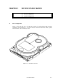
DISK DRIVES
PRODUCT MANUAL
C141-E116-01EN
REVISION RECORD
Edition
Date published
01
Oct., 2000
Revised contents
Specification No.: C141-E116-**EN
The contents of this manual is subject to change
without prior notice.
All Rights Reserved.
Copyright 2000 FUJITSU LIMITED
C141-E116-01EN
i
This page is intentionally left blank.
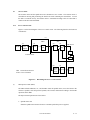
MANUAL ORGANIZATION
MPG3xxxAH-E
DISK DRIVES
PRODUCT
MANUAL
(C141-E116)
<This manual>
MPG3xxxAH-E
DISK DRIVES
MAINTENANCE
MANUAL
(C141-F050)
•
•
•
•
•
•
DEVICE OVERVIEW
DEVICE CONFIGURATION
INSTALLATION CONDITIONS
THEORY OF DEVICE OPERATION
INTERFACE
OPERATIONS
• MAINTENANCE AND DIAGNOSIS
• REMOVAL AND REPLACEMENT PROCEDURE
C141-E116-01EN
iii
This page is intentionally left blank.
PREFACE
This manual describes the MPG3xxxAH-E series, a 3.5-inch hard disk drive with a BUILT-IN controller
that is compatible with the ATA interface.
This manual explains, in detail, how to incorporate the hard disk drives into user systems.
This manual assumes that users have a basic knowledge of hard disk drives and their application in
computer systems.
This manual consists of the following six chapters:
Chapter 1
DEVICE OVERVIEW
Chapter 2
DEVICE CONFIGURATION
Chapter 3
INSTALLATION CONDITIONS
Chapter 4
THEORY OF DEVICE OPERATION
Chapter 5
INTERFACE
Chapter 6
OPERATIONS
In this manual, disk drives may be referred to as drives or devices.
C141-E116-01EN
v
Conventions for Alert Messages
This manual uses the following conventions to show the alert messages. An alert message consists of an
alert signal and alert statements. The alert signal consists of an alert symbol and a signal word or just a
signal word.
The following are the alert signals and their meanings:
This indicates a hazardous situation likely to result in serious personal
injury if the user does not perform the procedure correctly.
This indicates a hazardous situation could result in personal injury if the
user does not perform the procedure correctly.
This indicates a hazardous situation could result in minor or moderate
personal injury if the user does not perform the procedure correctly. This
alert signal also indicates that damages to the product or other property,
may occur if the user does not perform the procedure correctly.
This indicates information that could help the user use the product more
efficiently.
In the text, the alert signal is centered, followed below by the indented message. A wider line space
precedes and follows the alert message to show where the alert message begins and ends. The following is
an example:
(Example)
IMPORTANT
HA (host adapter) consists of address decoder, driver, and receiver.
ATA is an abbreviation of "AT attachment". The disk drive is
conformed to the ATA-4 interface
The main alert messages in the text are also listed in the “Important Alert Items.”
vi
C141-E116-01EN
LIABILITY EXCEPTION
"Disk drive defects" refers to defects that involve adjustment, repair, or replacement.
Fujitsu is not liable for any other disk drive defects, such as those caused by user misoperation or
mishandling, inappropriate operating environments, defects in the power supply or cable, problems of the
host system, or other causes outside the disk drive.
C141-E116-01EN
vii
This page is intentionally left blank.
CONTENTS
page
CHAPTER 1
DEVICE OVERVIEW..........................................................................................1 - 1
1.1
Features .................................................................................................................................1 - 1
1.1.1
Functions and performance ...................................................................................................1 - 1
1.1.2
Adaptability...........................................................................................................................1 - 2
1.1.3
Interface.................................................................................................................................1 - 2
1.2
Device Specifications ............................................................................................................1 - 4
1.2.1
Specifications summary.........................................................................................................1 - 4
1.2.2
Model and product number ...................................................................................................1 - 5
1.3
Power Requirements..............................................................................................................1 - 5
1.4
Environmental Specifications................................................................................................1 - 8
1.5
Acoustic Noise ......................................................................................................................1 - 8
1.6
Shock and Vibration..............................................................................................................1 - 9
1.7
Reliability..............................................................................................................................1 - 9
1.8
Error Rate..............................................................................................................................1 - 10
1.9
Media Defects .......................................................................................................................1 - 10
CHAPTER 2
DEVICE CONFIGURATION .............................................................................2 - 1
2.1
Device Configuration ............................................................................................................2 - 1
2.2
System Configuration ............................................................................................................2 - 3
2.2.1
ATA interface........................................................................................................................2 - 3
2.2.2
1 drive connection .................................................................................................................2 - 3
2.2.3
2 drives connection................................................................................................................2 - 3
CHAPTER 3
INSTALLATION CONDITIONS........................................................................3 - 1
3.1
Dimensions............................................................................................................................3 - 1
3.2
Handling Cautions.................................................................................................................3 - 3
3.2.1
General notes.........................................................................................................................3 - 3
3.2.2
Installation.............................................................................................................................3 - 3
3.2.3
Recommended equipments....................................................................................................3 - 3
3.3
Mounting ...............................................................................................................................3 - 4
3.4
Cable Connections.................................................................................................................3 - 8
3.4.1
Device connector...................................................................................................................3 - 8
C141-E116-01EN
ix
3.4.2
Cable connector specifications ..............................................................................................3 - 9
3.4.3
Device connection .................................................................................................................3 - 9
3.4.4
Power supply connector (CN1) .............................................................................................3 - 10
3.4.5
System configuration for Ultra DMA....................................................................................3 - 10
3.5
Jumper Settings .....................................................................................................................3 - 13
3.5.1
Location of setting jumpers ...................................................................................................3 - 13
3.5.2
Factory default setting ...........................................................................................................3 - 14
3.5.3
Jumper configuration.............................................................................................................3 - 14
CHAPTER 4
THEORY OF DEVICE OPERATION ...............................................................4 - 1
4.1
Outline...................................................................................................................................4 - 1
4.2
Subassemblies .......................................................................................................................4 - 1
4.2.1
Disk .......................................................................................................................................4 - 1
4.2.2
Head ......................................................................................................................................4 - 2
4.2.3
Spindle ..................................................................................................................................4 - 2
4.2.4
Actuator.................................................................................................................................4 - 3
4.2.5
Air filter.................................................................................................................................4 - 3
4.3
Circuit Configuration.............................................................................................................4 - 4
4.4
Power-on Sequence ...............................................................................................................4 - 6
4.5
Self-calibration ......................................................................................................................4 - 8
4.5.1
Self-calibration contents........................................................................................................4 - 8
4.5.2
Execution timing of self-calibration ......................................................................................4 - 9
4.5.3
Command processing during self-calibration ........................................................................4 - 9
4.6
Read/write Circuit .................................................................................................................4 - 10
4.6.1
Read/write preamplifier (PreAMP) .......................................................................................4 - 10
4.6.2
Write circuit ..........................................................................................................................4 - 10
4.6.3
Read circuit ...........................................................................................................................4 - 11
4.6.4
Synthesizer circuit .................................................................................................................4 - 12
4.7
Servo Control ........................................................................................................................4 - 13
4.7.1
Servo control circuit ..............................................................................................................4 - 13
4.7.2
Data-surface servo format .....................................................................................................4 - 16
4.7.3
Servo frame format................................................................................................................4 - 17
4.7.4
Actuator motor control ..........................................................................................................4 - 18
4.7.5
Spindle motor control............................................................................................................4 - 19
x
C141-E116-01EN
CHAPTER 5
INTERFACE .........................................................................................................5 - 1
5.1
Physical Interface ..................................................................................................................5 - 2
5.1.1
Interface signals.....................................................................................................................5 - 2
5.1.2
Signal assignment on the connector.......................................................................................5 - 3
5.2
Logical Interface ...................................................................................................................5 - 6
5.2.1
I/O registers...........................................................................................................................5 - 6
5.2.2
Command block registers ......................................................................................................5 - 8
5.2.3
Control block registers ..........................................................................................................5 - 13
5.3
Host Commands ....................................................................................................................5 - 13
5.3.1
Command code and parameters.............................................................................................5 - 14
5.3.2
Command descriptions ..........................................................................................................5 - 16
5.3.3
Error posting..........................................................................................................................5 - 76
5.4
Command Protocol................................................................................................................5 - 77
5.4.1
Data transferring commands from device to host ..................................................................5 - 77
5.4.2
Data transferring commands from host to device ..................................................................5 - 79
5.4.3
Commands without data transfer ...........................................................................................5 - 81
5.4.4
Other commands....................................................................................................................5 - 82
5.4.5
DMA data transfer commands...............................................................................................5 - 82
5.5
Ultra DMA feature set...........................................................................................................5 - 84
5.5.1
Overview ...............................................................................................................................5 - 84
5.5.2
Phases of operation................................................................................................................5 - 85
5.5.3
Ultra DMA data in commands...............................................................................................5 - 85
5.5.3.1 Initiating an Ultra DMA data in burst....................................................................................5 - 85
5.5.3.2 The data in transfer................................................................................................................5 - 86
5.5.3.3 Pausing an Ultra DMA data in burst .....................................................................................5 - 86
5.5.3.4 Terminating an Ultra DMA data in burst ..............................................................................5 - 87
5.5.4
Ultra DMA data out commands.............................................................................................5 - 89
5.5.4.1 Initiating an Ultra DMA data out burst..................................................................................5 - 89
5.5.4.2 The data out transfer..............................................................................................................5 - 90
5.5.4.3 Pausing an Ultra DMA data out burst ...................................................................................5 - 90
5.5.4.4 Terminating an Ultra DMA data out burst ............................................................................5 - 91
5.5.5
Ultra DMA CRC rules...........................................................................................................5 - 93
5.5.6
Series termination required for Ultra DMA...........................................................................5 - 94
5.6
Timing ...................................................................................................................................5 - 95
5.6.1
PIO data transfer ...................................................................................................................5 - 95
5.6.2
Multiword data transfer .........................................................................................................5 - 96
C141-E116-01EN
xi
5.6.3
Ultra DMA data transfer........................................................................................................5 - 97
5.6.3.1 Initiating an Ultra DMA data in burst....................................................................................5 - 97
5.6.3.2 Ultra DMA data burst timing requirements ...........................................................................5 - 98
5.6.3.3 Sustained Ultra DMA data in burst .......................................................................................5 - 101
5.6.3.4 Host pausing an Ultra DMA data in burst .............................................................................5 - 102
5.6.3.5 Device terminating an Ultra DMA data in burst....................................................................5 - 103
5.6.3.6 Host terminating an Ultra DMA data in burst .......................................................................5 - 104
5.6.3.7 Initiating an Ultra DMA data out burst..................................................................................5 - 105
5.6.3.8 Sustained Ultra DMA data out burst .....................................................................................5 - 106
5.6.3.9 Device pausing an Ultra DMA data out burst........................................................................5 - 107
5.6.3.10 Host terminating an Ultra DMA data out burst .....................................................................5 - 108
5.6.3.11 Device terminating an Ultra DMA data in burst....................................................................5 - 109
5.6.4
Power-on and reset ................................................................................................................5 - 110
CHAPTER 6
OPERATIONS ......................................................................................................6 - 1
6.1
Device Response to the Reset................................................................................................6 - 1
6.1.1
Response to power-on ...........................................................................................................6 - 2
6.1.2
Response to hardware reset ...................................................................................................6 - 3
6.1.3
Response to software reset ....................................................................................................6 - 4
6.1.4
Response to diagnostic command..........................................................................................6 - 5
6.2
Address Translation...............................................................................................................6 - 6
6.2.1
Default parameters ................................................................................................................6 - 6
6.2.2
Logical address......................................................................................................................6 - 7
6.3
Power Save............................................................................................................................6 - 8
6.3.1
Power save mode...................................................................................................................6 - 8
6.3.2
Power commands ..................................................................................................................6 - 10
6.4
Defect Management...............................................................................................................6 - 10
6.4.1
Spare area..............................................................................................................................6 - 11
6.4.2
Alternating defective sectors .................................................................................................6 - 11
6.5
Read-Ahead Cache ................................................................................................................6 - 13
6.5.1
Data buffer configuration ......................................................................................................6 - 13
6.5.2
Caching operation .................................................................................................................6 - 14
6.5.3
Usage of read segment...........................................................................................................6 - 15
6.6
Write Cache...........................................................................................................................6 - 20
xii
C141-E116-01EN
FIGURES
page
1.1
Current fluctuation (Typ.) when power is turned on .............................................................1 - 7
2.1
Disk drive outerview .............................................................................................................2 - 1
2.2
1 drive system configuration .................................................................................................2 - 3
2.3
2 drives configuration............................................................................................................2 - 3
3.1
Dimensions............................................................................................................................3 - 2
3.2
Handling cautions..................................................................................................................3 - 3
3.3
Direction................................................................................................................................3 - 4
3.4
Limitation of side-mounting ..................................................................................................3 - 5
3.5
Mounting frame structure ......................................................................................................3 - 5
3.6
Surface temperature measurement points ..............................................................................3 - 6
3.7
Service area ...........................................................................................................................3 - 7
3.8
Connector locations...............................................................................................................3 - 8
3.9
Cable connections .................................................................................................................3 - 9
3.10
Power supply connector pins (CN1)......................................................................................3 - 10
3.11
Cable configuration ...............................................................................................................3 - 11
3.12
Cable type detection using CBLID- signal
(Host sensing the condition of the CBLID- signal) ...............................................................3 - 12
3.13
Cable type detection using IDENTIFY DEVICE data
(Device sensing the condition of the CBLID- signal)............................................................3 - 12
3.14
Jumper location .....................................................................................................................3 - 13
3.15
Factory default setting ...........................................................................................................3 - 14
3.16
Jumper setting of master or slave device ...............................................................................3 - 14
3.17
Jumper setting of Cable Select ..............................................................................................3 - 15
3.18
Example (1) of Cable Select..................................................................................................3 - 15
3.19
Example (2) of Cable Select..................................................................................................3 - 15
4.1
Head structure .......................................................................................................................4 - 2
4.2
MPG3xxxAH-E Block diagram ............................................................................................4 - 5
4.3
Power-on operation sequence................................................................................................4 - 7
4.4
Block diagram of servo control circuit ..................................................................................4 - 13
4.5
Physical sector servo configuration on disk surface ..............................................................4 - 15
4.6
96 servo frames in each track ................................................................................................4 - 17
5.1
Execution example of READ MULTIPLE command ...........................................................5 - 19
5.2
Read Sector(s) command protocol ........................................................................................5 - 78
C141-E116-01EN
xiii
5.3
Protocol for command abort..................................................................................................5 - 79
5.4
WRITE SECTOR(S) command protocol ..............................................................................5 - 80
5.5
Protocol for the command execution without data transfer ...................................................5 - 81
5.6
Normal DMA data transfer....................................................................................................5 - 83
5.7
Ultra DMA termination with pull-up or pull-down ...............................................................5 - 94
5.8
PIO data transfer timing ........................................................................................................5 - 95
5.9
Multiword DMA data transfer timing (mode 2) ....................................................................5 - 96
5.10
Initiating an Ultra DMA data in burst....................................................................................5 - 97
5.11
Sustained Ultra DMA data in burst .......................................................................................5 - 101
5.12
Host pausing an Ultra DMA data in burst .............................................................................5 - 102
5.13
Device terminating an Ultra DMA data in burst....................................................................5 - 103
5.14
Host terminating an Ultra DMA data in burst .......................................................................5 - 104
5.15
Initiating an Ultra DMA data out burst..................................................................................5 - 105
5.16
Sustained Ultra DMA data out burst .....................................................................................5 - 106
5.17
Device pausing an Ultra DMA data out burst........................................................................5 - 107
5.18
Host terminating an Ultra DMA data out burst .....................................................................5 - 108
5.19
Device terminating an Ultra DMA data out burst..................................................................5 - 109
5.20
Power-on Reset Timing.........................................................................................................5 - 110
6.1
Response to power-on ...........................................................................................................6 - 2
6.2
Response to hardware reset ...................................................................................................6 - 3
6.3
Response to software reset ....................................................................................................6 - 4
6.4
Response to diagnostic command..........................................................................................6 - 5
6.5
Address translation (example in CHS mode) ........................................................................6 - 7
6.6
Address translation (example in LBA mode) ........................................................................6 - 8
6.7
Sector slip processing............................................................................................................6 - 11
6.8
Alternate cylinder assignment ...............................................................................................6 - 12
6.9
Data buffer configuration ......................................................................................................6 - 13
xiv
C141-E116-01EN
TABLES
page
1.1
Specifications ........................................................................................................................1 - 4
1.2
Model names and product numbers.......................................................................................1 - 5
1.3
Current and power dissipation...............................................................................................1 - 6
1.4
Environmental specifications ................................................................................................1 - 8
1.5
Acoustic noise specification ..................................................................................................1 - 8
1.6
Shock and vibration specification..........................................................................................1 - 9
3.1
Surface temperature measurement points and standard values..............................................3 - 6
3.2
Cable connector specifications ..............................................................................................3 - 9
4.1
Transfer rate of each zone .....................................................................................................4 - 12
5.1
Interface signals.....................................................................................................................5 - 2
5.2
Signal assignment on the interface connector........................................................................5 - 3
5.3
I/O registers...........................................................................................................................5 - 7
5.4
Command code and parameters.............................................................................................5 - 14
5.5
Information to be read by IDENTIFY DEVICE command...................................................5 - 29
5.6
Features register values and settable modes ..........................................................................5 - 36
5.7
Diagnostic code .....................................................................................................................5 - 40
5.8
Features Register values (subcommands) and functions........................................................5 - 50
5.9
Device attribute data structure...............................................................................................5 - 53
5.10
Warranty failure threshold data structure ..............................................................................5 - 54
5.11
Log directory data structure...................................................................................................5 - 59
5.12
Error logging data structure...................................................................................................5 - 60
5.13
Self Test log data structure....................................................................................................5 - 61
5.14
Contents of security password ...............................................................................................5 - 63
5.15
Contents of SECURITY SET PASSWORD data..................................................................5 - 68
5.16
Relationship between combination of Identifier and Security level,
and operation of the lock function.........................................................................................5 - 68
5.17
Command code and parameters.............................................................................................5 - 76
5.18
Recommended series termination for Ultra DMA.................................................................5 - 94
5.19
Ultra DMA data burst timing requirements ...........................................................................5 - 98
5.20
Ultra DMA sender and recipient timing requirements...........................................................5 - 100
6.1
Default parameters ................................................................................................................6 - 6
C141-E116-01EN
xv
This page is intentionally left blank.
CHAPTER 1
DEVICE OVERVIEW
1.1
Features
1.2
Device Specifications
1.3
Power Requirements
1.4
Environmental Specifications
1.5
Acoustic Noise
1.6
Shock and Vibration
1.7
Reliability
1.8
Error Rate
1.9
Media Defects
Overview and features are described in this chapter, and specifications and power requirement are
described.
The MPG3xxxAH-E series are a 3.5-inch hard disk drive with a built-in ATA controller. The disk drive is
compact and reliable.
1.1
Features
1.1.1
Functions and performance
(1)
Compact
The disk has 1 or 2 disks of 95 mm (3.5 inches) diameter, and its height is 26.1 mm (1 inch).
(2)
Large capacity
The disk drive can record up to 20.49 GB (formatted) on one disk using the 48/52 EEPR4ML
recording method and 15 recording zone technology. The MPG3xxxAH-E series have a formatted
capacity of 20.49 GB to 40.99 GB respectively.
(3)
High-speed Transfer rate
The disk drive has an internal data rate up to 60.7 MB/s. The disk drive supports an external data
rate up to 16.7 MB/s (PIO mode 4, DMA mode 2), 66.6 MB/s (ultra DMA mode 4) or 100MB/s
(ultra DMA mode 5).
C141-E116-01EN
1-1
(4)
Average positioning time
Use of a rotary voice coil motor in the head positioning mechanism greatly increases the
positioning speed. The average positioning time is 8.5 ms (at read).
1.1.2
Adaptability
(1)
Power save mode
The power save mode feature for idle operation, stand by and sleep modes makes the disk drive
ideal for applications where power consumption is a factor.
(2)
Wide temperature range
The disk drive can be used over a wide temperature range (5°C to 55°C).
(3)
Low noise and vibration
In Ready status, the noise of the disk drive is only about 3.3 bels (MPG3409AH-E, Typical Sound
Power per ISO7779 and ISO9296).
1.1.3
Interface
(1)
Connection to interface
With the built-in ATA interface controller, the disk drive can be connected to an ATA interface of
a personal computer.
(2)
2MB data buffer
The disk drive uses a 2MB data buffer to transfer data between the host and the disk media.
In combination with the read-ahead cache system described in item (3) and the write cache
described in item (6), the buffer contributes to efficient I/O processing.
(3)
Read-ahead cache system
After the execution of a disk read command, the disk drive automatically reads the subsequent data
block and writes it to the data buffer (read ahead operation). This cache system enables fast data
access. The next disk read command would normally cause another disk access. But, if the read
ahead data corresponds to the data requested by the next read command, the data in the buffer can
be transferred instead.
(4)
Master/slave
The disk drive can be connected to ATA interface as daisy chain configuration. Drive 0 is a
master device, drive 1 is a slave device.
1-2
C141-E116-01EN
(5)
Error correction and retry by ECC
If a recoverable error occurs, the disk drive itself attempts error recovery. The 40 bytes ECC has
improved buffer error correction for correctable data errors.
(6)
Write cache
When the disk drive receives a write command, the disk drive posts the command completion at
completion of transferring data to the data buffer completion of writing to the disk media. This
feature reduces the access time at writing.
C141-E116-01EN
1-3
1.2
Device Specifications
1.2.1
Specifications summary
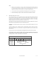
Table 1.1 shows the specifications of the disk drive.
Table 1.1
Specifications
MPG3204AH-E
MPG3307AH-E
MPG3409AH-E
20.49 GB
30.74 GB
40.99 GB
Number of Disks
1
2
2
Number of Heads
2
4
4
Formatted Capacity (*1)
Number of Cylinders
(User + Alternate & SA)
30,784 + 735 + 30
Bytes per Sector
512
Recording Method
48/52 CC2EPRML
Track Density
Bit Density
33,000 TPI
491,112 BPI
364,119 BPI
Rotational Speed
7,200 rpm
Average Latency
4.17 ms
Positioning time (Fast)
• Minimum
• Average
• Maximum
(Read) 0.8 ms typical, (Write) 1.0 ms typical
(Read) 8.5 ms typical, (Write) 9.5 ms typical
(Read) 16 ms typical, (Write) 17 ms typical
Positioning time (Slow)
• Minimum
• Average
• Maximum
(Read) 0.8 ms typical, (Write) 1.0 ms typical
(Read) 11 ms typical, (Write) 12 ms typical
(Read) 20 ms typical, (Write) 21 ms typical
Start/Stop time
• Start (0 rpm to Drive Read)
• Stop (at Power Down)
Typical: 8 sec.,
Typical: 20 sec.,
Interface
Data Transfer Rate
• To/From Media
• To/From Host
Maximum: 15 sec.
Maximum: 30 sec.
ATA–5
(Maximum Cable length: 0.46 m)
38.0 to 60.7 MB/s
27.9 to 49.7 MB/s
38.0 to 60.7 MB/s
16.7 MB/s Max. (burst PIO mode 4, burst DMA mode 2),
66.6 MB/s Max. (burst ultra DMA mode 4)
100.0 MB/s Max. (burst ultra DMA mode 5)
Data buffer
Physical Dimensions
(Height × Width × Depth)
491,112 BPI
2 MB
26.1 mm max. × 101.6 mm × 146.0 mm
(1.0” max. × 4.0” × 5.7”)
Weight
600 g or less
*1: Capacity under the LBA mode.
Under the CHS mode (normal BIOS specification), formatted capacity, number of cylinders, number of heads, and number of
sectors are as follows.
1-4
C141-E116-01EN
1.2.2
Model
Formatted Capacity
No. of Cylinder
No. of Heads
No. of Sectors
MPG3204AH-E
20,496 MB
16,383
16
63
MPG3307AH-E
30,743 MB
16,383
16
63
MPG3409AH-E
40,992 MB
16,383
16
63
Model and product number
Table 1.2 lists the model names and product numbers.
Table 1.2
Model Name
Capacity
(user area)
Mounting
Screw
MPG3204AH-E
20.49 GB
No. 6-32UNC
CA05762-B521
—
MPG3307AH-E
30.74 GB
No. 6-32UNC
CA05762-B544
—
MPG3409AH-E
40.99 GB
No. 6-32UNC
CA05762-B542
—
1.3
Power Requirements
(1)
Input Voltage
•
•
(2)
Model names and product numbers
Order No.
Remarks
+ 5 V ±5 %
+ 12 V ±8 %
Ripple
+12 V
+5 V
Maximum
200 mV (peak to peak)
100 mV (peak to peak)
Frequency
DC to 1 MHz
DC to 1 MHz
C141-E116-01EN
1-5
(3)
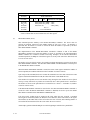
Current Requirements and Power Dissipation
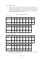
Table 1.3 lists the current and power dissipation.
Table 1.3
Current and power dissipation
Typical RMS current (*1) [mA]
Mode of Operation
Typical Power (*2) [watts]
+12 V
+5 V
Model
MPG
3204AH-E
MPG
3307AH-E
MPG
3409AH-E
All
Models
MPG
3204AH-E
MPG
3307AH-E
MPG
3409AH-E
Spin up
1950 peak
1950 peak
1950 peak
800 peak
27.4
27.4
27.4
Idle (Ready) (*3)
350
400
400
490
6.7
7.3
7.3
R/W (On Track) (*4)
370
450
450
600
7.4
8.4
8.4
Seek (Random) (*5)
480
540
540
570
8.6
9.3
9.3
Standby
18
18
18
120
0.8
0.8
0.8
Sleep
18
18
18
120
0.8
0.8
0.8
0.327 (A)
0.237 (B)
0.178 (B)
Energy efficiency (rank) (*6)
[watt / GB]
*1
Current is typical rms except for spin up.
*2
Power requirements reflect nominal values for +12V and +5V power.
*3
Idle mode is in effect when the drive is not reading, writing, seeking, or executing any commands. A portion of the R/W circuitry is powered down,
the spindle motor is up to speed and the Drive ready condition exists.
*4
R/W mode is defined as 50% read operations and 50% write operations on a single physical track.
*5
Seek/W/R mode is defined as 33% seek operations, 33% write operations, and 33% read operations.
*6
Energy efficiency based on the Law concerning the Rational Use of Energy indicates the value obtained by dividing power consumption by the storage
capacity. (Japan only)
1-6
C141-E116-01EN
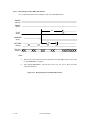
(4)
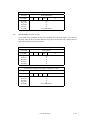
Current fluctuation (Typ.) when power is turned on
Note:
Maximum current is 1.95A.
Figure 1.1
(5)
Current fluctuation (Typ.) when power is turned on
Power on/off sequence
The voltage detector circuit monitors +5 V and +12 V. The circuit does not allow a write signal if
either voltage is abnormal. This prevents data from being destroyed and eliminates the need to be
concerned with the power on/off sequence.
C141-E116-01EN
1-7
1.4
Environmental Specifications
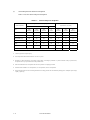
Table 1.4 lists the environmental specifications.
Table 1.4
Environmental specifications
Temperature
• Operating
5°C to 55°C (ambient)
5°C to 60°C (disk enclosure surface)
–40°C to 60°C
20°C/hour or less
• Non-operating
• Thermal Gradient
Humidity
• Operating
• Non-operating
• Maximum Wet Bulb
8% to 80%RH (Non-condensing)
5% to 85%RH (Non-condensing)
29°C
Altitude (relative to sea level)
• Operating
• Non-operating
–60 to 3,000 m (–200 to 10,000 ft)
–60 to 12,000 m (–200 to 40,000 ft)
1.5
Acoustic Noise
Table 1.5 lists the acoustic noise specification.
Table 1.5
Sound Power
per ISO 7779 and ISO9296
(Typical at 1m)
Sound Pressure
(Typical at 1m)
1-8
Acoustic noise specification
MPG3204AH-E
MPG3307AH-E
MPG3409AH-E
Idle mode (DRIVE READY)
3.6 bels
3.3 bels
Seek mode (Random)
4.0 bels
3.8 bels
Idle mode (DRIVE READY)
31 dBA
28 dBA
Seek mode (Random)
35 dBA
33 dBA
Model
C141-E116-01EN
1.6
Shock and Vibration
Table 1.6 lists the shock and vibration specification.
Table 1.6
Shock and vibration specification
Vibration (swept sine, one octave per minute)
• Operating
• Non-operating
4.9 m/s2 (0.5G0-P); 5 to 300 Hz
(without non-recovered errors)
39.2 m/s2 (4.0G0-P); 5 to 400 Hz (no damage)
Shock (half-sine pulse, Operating)
• 2 ms duration
392 m/s2 (40G0-P) (without non-recovered error)
Shock (half-sine pulse, Non-operating)
• 2 ms duration
2940 m/s2 (300G0-P) (Typical, no damage)
1.7
Reliability
(1)
Mean time between failures (MTBF)
The mean time between failures (MTBF) is 500,000 POH (power on hours) or more (operation: 24
hours/day, 7 days/week).
This does not include failures occurring during the first three months after installation.
MTBF is defined as follows:
MTBF=
Total operation time in all fields
number of device failure in all fields
(H)
"Disk drive defects" refers to defects that involve repair, readjustment, or replacement. Disk drive
defects do not include failures caused by external factors, such as damage caused by handling,
inappropriate operating environments, defects in the power supply host system, or interface cable.
(2)
Mean time to repair (MTTR)
The mean time to repair (MTTR) is 30 minutes or less, if repaired by a specialist maintenance staff
member.
(3)
CSS cycle
The number of CSS must be less than 50,000.
C141-E116-01EN
1-9
(4)
Service life
In situations where management and handling are correct, the disk drive requires no overhaul for
five years when the DE surface temperature is less than 48°C. When the DE surface temperature
exceeds 48°C, the disk drives requires no overhaul for five years or 20,000 hours of operation,
whichever occurs first. Refer to item (3) in Subsection 3.3 for the measurement point of the DE
surface temperature.
(5)
Data assurance in the event of power failure
Except for the data block being written to, the data on the disk media is assured in the event of any
power supply abnormalities. This does not include power supply abnormalities during disk media
initialization (formatting) or processing of defects (alternative block assignment).
1.8
Error Rate
Known defects, for which alternative blocks can be assigned, are not included in the error rate
count below. It is assumed that the data blocks to be accessed are evenly distributed on the disk
media.
(1)
Unrecoverable read error
Read errors that cannot be recovered by read retries without user's retry and ECC corrections shall
occur no more than 10 times when reading data of 1015 bits. Read retries are executed according to
the disk drive's error recovery procedure, and include read retries accompanying head offset
operations.
(2)
Positioning error
Positioning (seek) errors that can be recovered by one retry shall occur no more than 10 times in
107 seek operations.
1.9
Media Defects
Defective sectors are replaced with alternates when the disk is formatted prior to shipment from the
factory (low level format). Thus, the host sees a defect-free device.
Alternate sectors are automatically accessed by the disk drive. The user need not be concerned
with access to alternate sectors.
Chapter 6 describes the low level format at shipping.
1 - 10
C141-E116-01EN
CHAPTER 2
2.1
DEVICE CONFIGURATION
2.1
Device Configuration
2.2
System Configuration
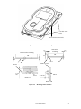
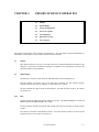
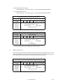
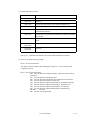
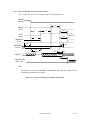
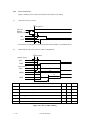
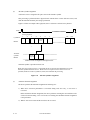
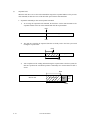
Device Configuration
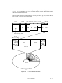
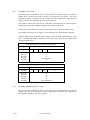
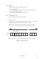
Figure 2.1 shows the disk drive. The disk drive consists of a disk enclosure (DE), read/write
preamplifier, and controller PCA. The disk enclosure contains the disk media, heads, spindle
motors actuators, and a circulating air filter.
Figure 2.1
Disk drive outerview
C141-E116-01EN
2-1
(1)
Disk
The outer diameter of the disk is 95 mm. The inner diameter is 25 mm. The number of disks used
varies with the model, as described below. The disks are rated at over 50,000 start/stop
operations.
MPG3204AH-E: 1 disks
MPG3307AH-E: 2 disks
MPG3409AH-E: 2 disks
(2)
Head
The heads are of the contact start/stop (CSS) type. The head touches the disk surface while the
disk is not rotating and automatically lifts when the disk starts.
(3)
Spindle motor
The disks are rotated by a direct drive Hall-less DC motor.
(4)
Actuator
The actuator uses a revolving voice coil motor (VCM) structure which consumes low power and
generates very little heat. The head assembly at the tip of the actuator arm is controlled and
positioned by feedback of the servo information read by the read/write head. If the power is not on
or if the spindle motor is stopped, the head assembly stays in the specific CSS zone on the disk and
is fixed by a mechanical lock.
(5)
Air circulation system
The disk enclosure (DE) is sealed to prevent dust and dirt from entering. The disk enclosure
features a closed loop air circulation system that relies on the blower effect of the rotating disk.
This system continuously circulates the air through the recirculation filter to maintain the
cleanliness of the air in the disk enclosure.
(6)
Read/write circuit
The read/write circuit uses a LSI chip for the read/write preamplifier. It improves data reliability
by preventing errors caused by external noise.
(7)
Controller circuit
The controller circuit consists of a LSI chip to improve reliability. The high-speed microprocessor
unit (MPU) achieves a high-performance AT controller.
2-2
C141-E116-01EN
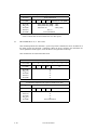
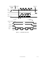
2.2
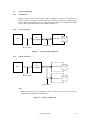
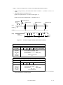
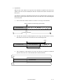
System Configuration
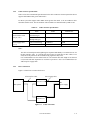
2.2.1
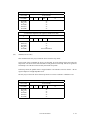
ATA interface
Figures 2.2 and 2.3 show the ATA interface system configuration. The drive has a 40-pin PC AT
interface connector and supports the PIO transfer till 16.7 MB/s (PIO mode 4), the DMA transfer
till 16.7 MB/s (Multiword DMA mode 2), the ultra DMA transfer till 66.6 MB/s (Ultra DMA
mode 4), and the ultra DMA transfer till 100 MB/s (Ultra mode 5).
2.2.2
1 drive connection
HA
(Host adaptor)
Host
ATA interface
AT bus
(Host interface)
Figure 2.2
2.2.3
Disk drive
1 drive system configuration
2 drives connection
HA
(Host adaptor)
Host
Disk drive #0
AT bus
(Host interface)
Disk drive #1
ATA interface
Note:
When the drive that is not conformed to ATA is connected to the disk drive is above
configuration, the operation is not guaranteed.
Figure 2.3
2 drives configuration
C141-E116-01EN
2-3
IMPORTANT
HA (host adapter) consists of address decoder, driver, and receiver.
ATA is an abbreviation of "AT attachment". The disk drive is
conformed to the ATA-5 interface.
At high speed data transfer (PIO mode 3, mode 4, DMA mode 2, ultra
DMA mode 4 or ultra DMA mode 5), occurrence of ringing or
crosstalk of the signal lines (AT bus) between the HA and the disk drive
may be a great cause of the obstruction of system reliability. Thus, it is
necessary that the capacitance of the signal lines including the HA and
cable does not exceed the ATA-3, ATA-4 and ATA-5 standard, and the
cable length between the HA and the disk drive should be as short as
possible.
2-4
C141-E116-01EN
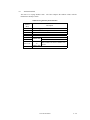
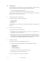
CHAPTER 3
3.1
INSTALLATION CONDITIONS
3.1
Dimensions
3.2
Handling Cautions
3.3
Mounting
3.4
Cable Connections
3.5
Jumper Settings
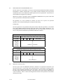
Dimensions
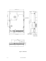
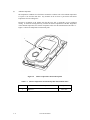
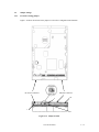
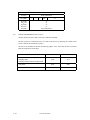
Figure 3.1 illustrates the dimensions of the disk drive and positions of the mounting screw holes.
All dimensions are in mm.
C141-E116-01EN
3-1
Figure 3.1 Dimensions
3-2
C141-E116-01EN
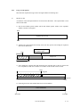
3.2
Handling Cautions
Please keep the following cautions, and handle the HDD under the safety environment.
3.2.1
General notes
ESD mat
Shock absorbing mat
Wrist strap
Use the Wrist strap.
Place the shock absorbing mat on the
operation table, and place ESD mat on it.
Do not hit HDD each other.
Do not stack when carrying.
Do not place HDD vertically
to avoid falling down.
Do not drop.
Figure 3.2
Handling cautions
3.2.2
Installation
(1)
Please use the driver of a low impact when you use an electric driver.
HDD is occasionally damaged by the impact of the driver.
(2)
Please observe the tightening torque of the screw strictly.
6-32UNC ······· Max. 0.59 N·m (6 Kg·cm)
3.2.3
Recommended equipments
ESD
Shock
Contents
Wrist strap
ESD mat
Low shock driver
Model
JX-1200-3056-8
76000DES (ASK7876)
SS-3000
C141-E116-01EN
Maker
SUMITOMO 3M
COMKYLE
HIOS
3-3
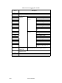
3.3
Mounting
(1)
Direction
Figure 3.3 illustrates normal direction for the disk drive. The disk drives can be mounted in any
direction.
Horizontal mounting with the PCB facing down
Figure 3.3
(2)
Direction
Frame
The disk enclosure (DE) body is connected to signal ground (SG) and the mounting frame is also
connected to signal ground. These are electrically shorted.
Note:
Use No.6-32UNC screw for the mounting screw and the screw length should satisfy the
specification in Figure 3.5.
(3)
Limitation of side-mounting
When the disk drive is mounted using the screw holes on both side of the disk drive, use two screw
holes shown in Figure 3.4.
Do not use the center hole. For screw length, see Figure 3.5.
3-4
C141-E116-01EN
Use these screw
holes
Do not use this screw holes
Figure 3.4
Limitation of side-mounting
Side surface
mounting
2.5
Bottom surface mounting
2.5
DE
DE
2.5
2
PCA
A
Frame of system
cabinet
B
Frame of system
cabinet
4.5 or
less
Screw
Screw
5.0 or less
Details of A
Details of B
Figure 3.5
Mounting frame structure
C141-E116-01EN
3-5
(4)
Ambient temperature
The temperature conditions for a disk drive mounted in a cabinet refer to the ambient temperature
at a point 3 cm from the disk drive. Pay attention to the air flow to prevent the DE surface
temperature from exceeding 60°C.
Provide air circulation in the cabinet such that the PCA side, in particular, receives sufficient
cooling. To check the cooling efficiency, measure the surface temperatures of the DE. Regardless
of the ambient temperature, this surface temperature must meet the standards listed in Table 3.1.
Figure 3.6 shows the temperature measurement point.
1
Figure 3.6
Table 3.1
Surface temperature measurement points and standard values
No.
1
3-6
Surface temperature measurement points
Measurement point
DE cover
Temperature
60°C max
C141-E116-01EN
(5)
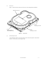
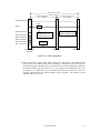
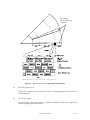
Service area
Figure 3.7 shows how the drive must be accessed (service areas) during and after installation.
- Mounting screw hole
[Q side]
- Mounting screw hole
[P side]
- Cable connection
- Mode setting switches
[R side]
- Mounting screw hole
Figure 3.7
(6)
Service area
External magnetic fields
Avoid mounting the disk drive near strong magnetic sources such as loud speakers. Ensure that the
disk drive is not affected by external magnetic fields.
C141-E116-01EN
3-7
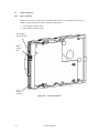
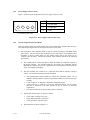
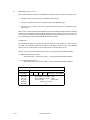
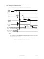
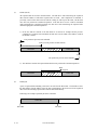
3.4
Cable Connections
3.4.1
Device connector
The disk drive has the connectors and terminals listed below for connecting external devices.
Figure 3.8 shows the locations of these connectors and terminals.
•
•
Power supply connector (CN1)
ATA interface connector (CN1)
Power supply
connector (CN1)
Mode
Setting
Pins
ATA
interface
connector
Figure 3.8
3-8
Connector locations
C141-E116-01EN
3.4.2
Cable connector specifications
Table 3.2 lists the recommended specifications for the cable connectors for Host system that do not
support Ultra DMA modes greater than mode 2.
For Host system that support Ultra DMA modes greater than mode 2, the 80-conductor cable
assemblies shall be used. The 80-conductor cable assemblies are manufactured by AMP or 3M.
Table 3.2
Cable connector specifications
Name
ATA interface cable
(40-pin, CN1)
Power supply cable
(CN1)
Model
Manufacturer
Cable socket
(closed-end type)
FCN-707B040-AU/B
Fujitsu
Cable socket
(through-end type)
FCN-707B040-AU/O
Fujitsu
Cable socket housing
1-480424-0
AMP
Contact
60617-4
AMP
Note :
The cable of twisted pairs and neighboring line separated individually is not allowed to use for
the host interface cable. It is because that the location of signal lines in these cables is not
fixed, and so the problem on the crosstalk among signal lines may occur.
It is recommended to use the ribbon cable for ATA interface that cable length is less than 46
cm (18 inch) and cable capacitance is less than 35 pico farad. Also it is recommended to use
AWG18 power supply cable.
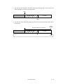
3.4.3
Device connection
Figure 3.9 shows how to connect the devices.
ATA interface cable
Power supply cable
Disk Drive #0
Host system
DC
power supply
Disk Drive #1
Figure 3.9
Cable connections
C141-E116-01EN
3-9
3.4.4
Power supply connector (CN1)
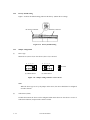
Figure 3.10 shows the pin assignment of the power supply connector (CN1).
1
2
3
4
1
+12VDC
2
+12V RETURN
3
+5V RETURN
4
+5VDC
(Viewed from cable side)
Figure 3.10 Power supply connector pins (CN1)
3.4.5
System configuration for Ultra DMA
Host system that support Ultra DMA transfer modes greater than mode 2 shall not share I/O ports.
They shall provide separate drivers and separate receivers for each cable.
a) The 80-conductor cable assemblies shall be used for systems operating at Ultra DMA modes
greater than 2. The 80-coductor cable assemblies may be used in place of 40-conductor cable
assemblies to improve signal quality for data transfer modes that do not require an 80conductor cable assembly. And the 80-conductor cable assembly shall meet the following
specifications.
1)
The assembly utilizes a fine pitch cable to double the number of conductors available to
the 40-pin connector. The grounds assigned by the interface are commoned with the
additional 40 conductors to provide a ground between each signal line and provide the
effect of a common ground plane.
2)
The cable assembly may contain up to 3 connectors which shall be uniquely colored as
follows. All connectors shall have position 20 blocked.
•
•
•
•
3)
Typical cable characteristics are shown as follows.
•
•
•
4)
3 - 10
The System Board Connector shall have a Blue base and Black retainer. Pin 34
(PDIAG-: CBLID-) shall be connected to ground and shall not be wired to the cable
assembly.
Connector Device “0” shall have a Black base and Black retainer.
Connector Device “1” shall have a Gray base and Black retainer. Pin 28 (CSEL)
shall not be connected to the cable (contact 28 may be removed to meet this
requirement).
The cable assembly may be printed with connector identifiers.
Cable: AWG 30 (pitch: 0.635 mm)
Single Ended impedance: typical 80 Ω.
Cable capacitance: typical 57 pF/m
The dimensions are shown in Figure 3.11.
C141-E116-01EN
254.0 to 457.2 mm
(10 to 18 inch)
127.0 to 304.8 mm
101.6 to 152.4 mm
(5 to 12 inch)
(4 to 6 inch)
Pin 40 (Ground)
open
Pin 34
Pin 34 contact
(PDIAG-:CBLID- signal)
Pin 30 (Ground)
Pin 26 (Ground)
Pin 24 (Ground)
Pin 22 (Ground)
Pin 19 (Ground)
Symbolizes Pin 34
Conductor being cut
Position 1
Pin 2 (Ground)
System Board
Connector
Connector 1
Connector 2
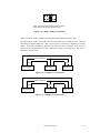
Figure 3.11 Cable configuration
b) Host system that do support Ultra DMA modes greater than mode 2 shall either connect
directly to the device without using a cable assembly, or determine the cable assembly type.
Determining the cable assembly type may be done either by the host sensing the condition of
the PDIAG-:CBLID- signal (see Figure 3.12), or by relying on information from the device
(see Figure 3.13). Hosts that rely on information from the device shall have a 0.047 µF
capacitor connected from the PDIAG-:CBLID- signal to ground. The tolerance on this
capacitor shall be 20% or less.
C141-E116-01EN
3 - 11
Host detected CBLID- below VIL
Host detected CBLID- above VIH
open
PDIAG-: CBLID- conductor
Host
Device 1
Device 0
PDIAG-: CBLID- conductor
Host
with 40-conductor cable
Device 1
Device 0
with 80-conductor cable
Figure 3.12 Cable type detection using CBLID- signal
(Host sensing the condition of the CBLID- signal)
IDENTIFY DEVICE information
word 93 bit13:1
Device detected CBLID- above VIH
open PDIAG-:CBLID- conductor
IDENTIFY DEVICE information
word 93 bit13:0
Device detected CBLID- below VIL
PDIAG-:CBLID- conductor
0.047 µF
±10% or
±20%
Host
0.047 µF
±10% or
±20%
Device 1
Device 0
Host
with 40-conductor cable
Device 1
with 80-conductor cable
Figure 3.13 Cable type detection using IDENTIFY DEVICE data
(Device sensing the condition of the CBLID- signal)
3 - 12
C141-E116-01EN
Device 0
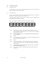
3.5
Jumper Settings
3.5.1
Location of setting jumpers
Figure 3.14 shows the location of the jumpers to select drive configuration and functions.
DC Power Connector
Interface Connector
2
40
1
1
Figure 3.14 Jumper location
C141-E116-01EN
3 - 13
3.5.2
Factory default setting
Figure 3.15 shows the default setting position at the factory. (Master device setting)
DC Power Connector
Interface Connector
Figure 3.15 Factory default setting
3.5.3
Jumper configuration
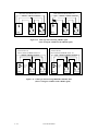
(1)
Device type
Master device (device #0) or slave device (device #1) is selected.
2
4 6 8
2
4 6 8
= shorted
1
3 5 7 9
(a) Master device
1
3 5 7 9
(b) Slave device
Figure 3.16 Jumper setting of master or slave device
Note:
When the device type is set by the jumper on the device, the device should not be configured
for cable selection.
(2)
Cable Select (CSEL)
In Cable Select mode, the device can be configured either master device or slave device. For use of
Cable Select function, Unique interface cable is needed.
3 - 14
C141-E116-01EN
2
4 6 8
1
3 5 7 9
CSEL connected to the interface cable selection
can be done by the special interface cable.
Figure 3.17 Jumper setting of Cable Select
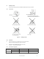
Figures 3.18 and 3.19 show examples of cable selection using unique interface cables.
By connecting the CSEL of the master device to the CSEL Line (conductor) of the cable and
connecting it to ground further, the CSEL is set to low level. The device is identified as a master
device. At this time, the CSEL of the slave device does not have a conductor. Thus, since the
slave device is not connected to the CSEL conductor, the CSEL is set to high level. The device is
identified as a slave device.
CSEL conductor
Open
GND
Host system
Master device
Slave device
Figure 3.18 Example (1) of Cable Select
CSEL conductor
GND
Host system
Open
Slave device
Master device
Figure 3.19 Example (2) of Cable Select
C141-E116-01EN
3 - 15
(3)
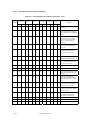
Special jumper settings
(a) 2.1 GB clip (Limit capacity to 2.1 GB) / 33.8 GB clip (Limit capacity to 33.8 GB)
If the drive cannot be recognized by system with legacy BIOS’s which do not allow single
volume sizes greater than approximately 2.1 GB, the following jumper settings should be
applied.
This jumper settings is also used as the 33.8 GB clip for MPG3409AH-E. (MPG3409AH-E
does not have the 2.1 GB clip feature.)
2
4 6 8
2
4 6 8
2
4 6 8
1
3 5 7 9
1
3 5 7 9
1
3 5 7 9
Master Device
Model
Slave Device
Cable Select
No. of cylinders
No. of heads
No. of sectors
Capacity
MPG3204AH-E
4,092
16
63
2.1 GB
MPG3307AH-E
4,092
16
63
2.1 GB
MPG3409AH-E
16,383
16
63
33.8 GB
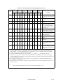
(b) Slave present
If the slave device does not use the Device Active/Slave Present (DASP–) signal to indicate its
presence, the device is configured as a Master with slave present when the following jumper
settings is applied.
2
4 6 8
1
3 5 7 9
Slave present
NOTE:
The following Jumper Plug is the recommended specification for jumper setting on this device.
Parts name
Jumper Plug
3 - 16
Parts number
Manufacturer
Remarks
IMAS-9251H-GF
IRISO ELECTRONICS CO., LTD
2.54 mm Pitch
206-A-BLK
OUPIIN ENTERPRISE CO., LTD
! 0.64 mm
C141-E116-01EN
CHAPTER 4
THEORY OF DEVICE OPERATION
4.1
Outline
4.2
Subassemblies
4.3
Circuit Configuration
4.4
Power-on sequence
4.5
Self-calibration
4.6
Read/write Circuit
4.7
Servo Control
This chapter explains basic design concepts of the disk drive. Also, this chapter explains subassemblies of
the disk drive, each sequence, servo control, and electrical circuit blocks.
4.1
Outline
This chapter consists of two parts. First part (Section 4.2) explains mechanical assemblies of the
disk drive. Second part (Sections 4.3 through 4.7) explains a servo information recorded in the
disk drive and drive control method.
4.2
Subassemblies
The disk drive consists of a disk enclosure (DE) and printed circuit assembly (PCA).
The DE contains all movable parts in the disk drive, including the disk, spindle, actuator,
read/write head, and air filter. For details, see Subsections 4.2.1 to 4.2.5.
The PCA contains the control circuits for the disk drive. The disk drive has one PCA. For details,
see Sections 4.3.
4.2.1
Disk
The DE contains the disks with an outer diameter of 95 mm. The MPG3204AH-E has 1 disk, and
MPG3307AH-E and MPG3409AH-E have 2 disk.
The head contacts the disk each time the disk rotation stops; the life of the disk is 50,000 contacts
or more.
Servo data is recorded on each cylinder (total 96). Servo data written at factory is read out by the
read/write head. For servo data, see Section 4.7.
C141-E116-01EN
4-1
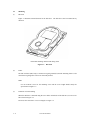
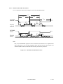
4.2.2
Head
Figure 4.1 shows the read/write head structures. The Numerals 0 to 3 indicate read/write heads.
These heads are raised from the disk surface as the spindle motor approaches the rated rotation
speed.
MPG3204AH-E
Spindle
Actuator
1
0
MPG3307AH-E / MPG3409AH-E
Spindle
Actuator
3
2
1
0
Figure 4.1
4.2.3
Head structure
Spindle
The spindle consists of a disk stack assembly and spindle motor. The disk stack assembly is
activated by the direct drive sensor-less DC spindle motor, which has a speed of 7,200 rpm. The
spindle is controlled with detecting a PHASE signal generated by counter electromotive voltage of
the spindle motor at starting. After that, the rotational speed is kept with detecting a servo
information.
4-2
C141-E116-01EN
4.2.4
Actuator
The actuator consists of a voice coil motor (VCM) and a head carriage. The VCM moves the head
carriage along the inner or outer edge of the disk. The head carriage position is controlled by
feeding back the difference of the target position that is detected and reproduced from the servo
information read by the read/write head.
4.2.5
Air filter
There are two types of air filters: a breather filter and a circulation filter.
The breather filter makes an air in and out of the DE to prevent unnecessary pressure around the
spindle when the disk starts or stops rotating. When disk drives are transported under conditions
where the air pressure changes a lot, filtered air is circulated in the DE.
The circulation filter cleans out dust and dirt from inside the DE. The disk drive cycles air
continuously through the circulation filter through an enclosed loop air cycle system operated by a
blower on the rotating disk.
C141-E116-01EN
4-3
4.3
Circuit Configuration
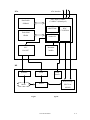
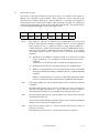
Figure 4.2 shows the disk drive circuit configuration.
(1)
Read/write circuit
The read/write circuit consists of two LSIs; read/write preamplifier (PreAMP) and read channel
(RDC).
The PreAMP consists of the write current switch circuit, that flows the write current to the head
coil, and the voltage amplifier circuit, that amplitudes the read output from the head.
The RDC is the read demodulation circuit using the Extended Partial Response Class 4 (EPR4),
and contains the Viterbi detector, programmable filter, adaptable transversal filter, times base
generator, and data separator circuits. The RDC also contains the 48/52 group coded recording
(GCR) encoder and decoder and servo demodulation circuit.
(2)
Servo circuit
The position and speed of the voice coil motor are controlled by 2 closed-loop servo using the
servo information recorded on the data surface. The servo information is an analog signal
converted to digital for processing by a MPU and then reconverted to an analog signal for control
of the voice coil motor.
(3)
Spindle motor driver circuit
The circuit measures the interval of a PHASE signal generated by counter-electromotive voltage of
a motor, or servo mark at the MPU and controls the motor speed comparing target speed.
(4)
Controller circuit
Major functions are listed below.
•
•
•
•
•
•
4-4
Data buffer management
ATA interface control and data transfer control
Sector format control
Defect management
ECC control
Error recovery and self-diagnosis
C141-E116-01EN
ATA Interface
PCA
HDC & MCU & RDC
CL-SH8671 (Himalaya-2)
Data Buffer
SDRAM
MCU
ARM7TDMI
HDC
CL-SH7660
Flash ROM
RDC
Number-B
FROM
SVC
Resonator
HA13627
20MHz
DE
SP Motor
VCM
Temp.
Sensor
R/W Pre-Amp
HEAD
Media
SR1756 or
M61850
Figure 4.2
MPG3xxxAH Block diagram
C141-E116-01EN
4-5
4.4
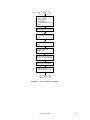
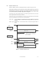
Power-on Sequence
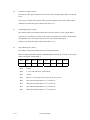
Figure 4.3 describes the operation sequence of the disk drive at power-on. The outline is described
below.
a) After the power is turned on, the disk drive executes the MPU bus test, internal register
read/write test, and work RAM read/write test. When the self-diagnosis terminates
successfully, the disk drive starts the spindle motor.
b) The disk drive executes self-diagnosis (data buffer read/write test) after enabling response to
the ATA bus.
c) After confirming that the spindle motor has reached rated speed, the disk drive releases the
heads from the actuator magnet lock mechanism by applying current to the VCM. This
unlocks the heads which are parked at the inner circumference of the disks.
d) The disk drive positions the heads onto the SA area and reads out the system information.
e) The disk drive executes self-seek-calibration. This collects data for VCM torque and
mechanical external forces applied to the actuator, and updates the calibrating value.
f) The drive becomes ready. The host can issue commands.
4-6
C141-E116-01EN
Power on
a)
Start
Self-diagnosis 1
• MPU bus test
• Inner register
write/read test
• Work RAM write/read
test
The spindle motor starts.
b)
Self-diagnosis 2
• Data buffer write/read
test
c)
Confirming spindle motor
speed
Release heads from
actuator lock
d)
Initial on-track and read
out of system information
e)
Execute self-calibration
f)
Drive ready state
(command waiting state)
End
Figure 4.3
Power-on operation sequence
C141-E116-01EN
4-7
4.5
Self-calibration
The disk drive occasionally performs self-calibration in order to sense and calibrate mechanical
external forces on the actuator, and VCM torque. This enables precise seek and read/write
operations.
4.5.1
Self-calibration contents
(1)
Sensing and compensating for external forces
The actuator suffers from torque due to the FPC forces and winds accompanying disk revolution.
The torque vary with the disk drive and the cylinder where the head is positioned. To execute
stable fast seek operations, external forces are occasionally sensed.
The firmware of the drive measures and stores the force (value of the actuator motor drive current)
that balances the torque for stopping head stably. This includes the current offset in the power
amplifier circuit and DAC system.
The forces are compensated by adding the measured value to the specified current value to the
power amplifier. This makes the stable servo control.
To compensate torque varying by the cylinder, the disk is divided into 28 areas from the innermost
to the outermost circumference and the compensating value is measured at the measuring cylinder
on each area at factory calibration. The measured values are stored in the SA cylinder. In the selfcalibration, the compensating value is updated using the value in the SA cylinder.
(2)
Compensating open loop gain
Torque constant value of the VCM has a dispersion for each drive, and varies depending on the
cylinder that the head is positioned. To realize the high speed seek operation, the value that
compensates torque constant value change and loop gain change of the whole servo system due to
temperature change is measured and stored.
For sensing, the firmware mixes the disturbance signal to the position signal at the state that the
head is positioned to any cylinder. The firmware calculates the loop gain from the position signal
and stores the compensation value against to the target gain as ratio.
For compensating, the direction current value to the power amplifier is multiplied by the
compensation value. By this compensation, loop gain becomes constant value and the stable servo
control is realized.
To compensate torque constant value change depending on cylinder, whole cylinders from most
inner to most outer cylinder are divided into 14 partitions at calibration in the factory, and the
compensation data is measured for representative cylinder of each partition. This measured value
is stored in the SA area. The compensation value at self-calibration is calculated using the value in
the SA area.
4-8
C141-E116-01EN
4.5.2
Execution timing of self-calibration
Self-calibration is executed when:
•
•
The power is turned on.
The self-calibration execution timechart of the disk drive specifies self-calibration.
The disk drive performs self-calibration according to the timechart based on the time elapsed from
power-on. After power-on, self-calibration is performed about every 30 minutes, when the host
command is not issued for 15 seconds.
4.5.3
Command processing during self-calibration
If the disk drive receives a command execution request from the host while executing selfcalibration according to the timechart, the disk drive terminates self-calibration and starts
executing the command precedingly. In other words, if a disk read or write service is necessary,
the disk drive positions the head to the track requested by the host, reads or writes data. Then
restarts calibration if the host command is not issued for 15 seconds.
This enables the host to execute the command without waiting for a long time, even when the disk
drive is performing self-calibration. Only the first command execution wait time is about
maximum 100 ms.
C141-E116-01EN
4-9
4.6
Read/write Circuit
The read/write circuit consists of the read/write preamplifier (PreAMP), the write circuit, the read
circuit, and the synthesizer in the read channel (RDC).
4.6.1
Read/write preamplifier (PreAMP)
One PreAMP is mounted on the FPC. The PreAMP consists of a 4-channel read preamplifier and
a write current switch and senses a write error. Each channel is connected to each data head. The
head IC switches the heads by the serial port (SDEN, SCLK, SDATA). The IC generates a write
error sense signal (WUS) when a write error occurs due to head short-circuit or head
disconnection.
4.6.2
Write circuit
The write data is output from the hard disk controller (HDC) with the NRZ data format, and sent to
the encoder circuit in the RDC with synchronizing with the write clock. The NRZ write data is
converted from 48-bits data to 52-bits data by the encoder circuit then sent to the PreAMP, and the
data is written onto the media.
(1)
48/52 GCR
The disk drive converts data using the 48/52 group coded recording (GCR) algorithm.
(2)
Write precompensation
Write precompensation compensates, during a write process, for write non-linearity generated at
reading.
4 - 10
C141-E116-01EN
4.6.3
Read circuit
The head read signal from the PreAMP is regulated by the variable gain amplifier (VGA) circuit.
Then the output is converted into the sampled read data pulse by the programmable filter circuit
and the adaptive equalizer circuit. This clock signal is converted into the NRZ data by the 48/52
GCR decoder circuit based on the read data maximum-likelihood-detected by the Viterbi detection
circuit, then is sent to the HDC.
(1)
VGA circuit
The VGA circuit automatically regulates the output amplitude to a constant value even when the
input amplitude level fluctuates. The VGA output is maintained at a constant level even when the
head output fluctuates due to the head characteristics or outer/inner head positions.
(2)
Programmable filter
The programmable filter circuit has a low-pass filter function that eliminates unnecessary high
frequency noise component and a high frequency boost-up function that equalizes the waveform of
the read signal.
Cut-off frequency of the low-pass filter and boost-up gain are controlled from each DAC circuit in
read channel. The MPU optimizes the cut-off frequency and boost-up gain according to the
transfer frequency of each zone.
(3)
FIR (Digital Finite Impulse Response Equalization Filter) adaptation circuit
The FIR provides support for changing equalization needs from head to head and zone to zone.
The FIR is a specialized digital filter with ten independently controlled coefficients.
(4)
Viterbi detection circuit
The Viterbi detection circuit demodulates data according to the survivor path sequence.
(5)
Data separator circuit
The data separator circuit generates clocks in synchronization with the output of the adaptive
equalizer circuit. To write data, the VFO circuit generates clocks in synchronization with the clock
signals from a synthesizer.
(6)
48/52 GCR decoder
This circuit converts the 52-bits read data into the 48-bits NRZ data.
C141-E116-01EN
4 - 11
4.6.4
Synthesizer circuit
The drive uses constant density recording to increase total capacity. This is different from the
conventional method of recording data with a fixed data transfer rate at all data area. In the
constant density recording method, data area is divided into zones by radius and the data transfer
rate is set so that the recording density of the inner cylinder of each zone is nearly constant. The
drive divides data area into 15 zones to set the data transfer rate. Table 4.1 describes the data
transfer rate and recording density (BPI) of each zone.
Table 4.1
Transfer rate of each zone
MPG3307AH-E
Zone
Cylinder
Transfer rate
[MB/s]
Zone
Cylinder
Transfer rate
[MB/s]
0
1
2
3
4
5
6
7
0
to
2207
2208
to
4223
4224
to
7231
7232
to
9823
9824
to
13119
13120
to
15615
15616
to
17087
17088
to
19359
49.73
48.87
47.22
45.79
43.61
41.88
41.01
39.28
8
9
10
11
12
13
14
19360
to
22047
22048
to
23839
23840
to
25247
25248
to
26591
26592
to
28767
28768
to
30175
30176
to
30783
37.22
35.77
34.62
33.45
31.43
30.12
27.92
MPG3204AH-E / MPG3409AH-E
Zone
Cylinder
Transfer rate
[MB/s]
Zone
Cylinder
Transfer rate
[MB/s]
0
1
2
3
4
5
6
7
0
to
2783
2784
to
5567
5568
to
8351
8352
to
11263
11264
to
13439
13440
to
16095
16096
to
17983
17984
to
19839
60.71
60.71
60.71
60.71
59.22
56.86
54.90
52.94
8
9
10
11
12
13
14
19840
to
22175
22176
to
23583
23584
to
25087
25088
to
26719
26720
to
28575
28576
to
29951
29952
to
30783
50.35
48.82
47.06
45.10
42.75
40.94
38.04
The MPU transfers the data transfer rate setup data to the RDC that includes the time base
generator circuit to change the data transfer rate.
4 - 12
C141-E116-01EN
4.7
Servo Control
The actuator motor and the spindle motor are submitted to servo control. The actuator motor is
controlled for moving and positioning the head to the track containing the desired data. To turn
the disk at a constant velocity, the actuator motor is controlled according to the servo data that is
written on the data side beforehand.
4.7.1
Servo control circuit
Figure 4.4 is the block diagram of the servo control circuit. The following describes the functions
of the blocks:
(1)
MPU
Head
(2)
Servo
burst
capture
(3)
ADC
(4)
DSP
unit
SVC
(5)
DAC
VCM current
P.
Amp.
CSR
Position Sense
VCM
(6)
Spindle
motor
control
CSR: Current Sense Resistor
VCM: Voice Coil Motor
Figure 4.4
(1)
(7)
Driver
Spindle
motor
Block diagram of servo control circuit
Microprocessor unit (MPU)
The MPU includes DSP unit, etc., and the MPU starts the spindle motor, moves the heads to the
reference cylinders, seeks the specified cylinder, and executes calibration according to the internal
operations of the MPU.
The major internal operations are listed below.
a. Spindle motor start
Starts the spindle motor and accelerates it to normal speed when power is applied.
C141-E116-01EN
4 - 13
b. Move head to reference cylinder
Drives the VCM to position the head at the any cylinder in the data area. The logical initial
cylinder is at the outermost circumference (cylinder 0).
c. Seek to specified cylinder
Drives the VCM to position the head to the specified cylinder.
d. Calibration
Senses and stores the thermal offset between heads and the mechanical forces on the actuator,
and stores the calibration value.
4 - 14
C141-E116-01EN
Servo frame
(96 servo frames per
revolution)
Figure 4.5
(2)
Physical sector servo configuration on disk surface
Servo burst capture circuit
The four servo signals can be synchronously detected by the DEMOD signal (internal), full-wave
rectified integrated.
(3)
A/D converter (ADC)
The A/D converter (ADC) receives the servo signals are integrated, converts them to digital, and
transfers the digital signal to the DSP unit.
C141-E116-01EN
4 - 15
(4)
D/A converter (DAC)
The D/A converter (DAC) converts the VCM drive current value (digital value) calculated by the
DSP unit into analog values and transfers them to the power amplifier.
(5)
Power amplifier
The power amplifier feeds currents, corresponding to the DAC output signal voltage to the VCM.
(6)
Spindle motor control circuit
The spindle motor control circuit controls the sensor-less spindle motor. This circuit detects
number of revolution of the motor by the interrupt generated periodically, compares with the target
revolution speed, then flows the current into the motor coil according to the differentiation
(aberration).
(7)
Driver circuit
The driver circuit is a power amplitude circuit that receives signals from the spindle motor control
circuit and feeds currents to the spindle motor.
(8)
VCM current sense resistor (CSR)
This resistor controls current at the power amplifier by converting the VCM current into voltage
and feeding back.
4.7.2
Data-surface servo format
Figure 4.5 describes the physical layout of the servo frame. The three areas indicated by (1) to (3)
in Figure 4.6 are described below.
(1)
Inner guard band
The head is in contact with the disk in this space when the spindle starts turning or stops, and the
rotational speed of the spindle can be controlled on this cylinder area for head moving.
(2)
Data area
This area is used as the user data area and SA area.
(3)
Outer guard band
This area is located at outer position of the user data area, and the rotational speed of the spindle
can be controlled on this cylinder area for head moving.
4 - 16
C141-E116-01EN
4.7.3
Servo frame format
As the servo information, the drive uses the two-phase servo generated from the gray code and Pos
A to D. This servo information is used for positioning operation of radius direction and position
detection of circumstance direction.
The servo frame consists of 5 blocks; write/read recovery, servo mark, gray code, Pos A to D and
PAD. Figure 4.6 shows the servo frame format.
0.72 µs
0.17 µs
0.16 µs
0.53 µs 0.74 µs 0.56 µs 0.56 µs 0.56 µs 0.80 µs
1.81 µs
SCD
PA
ASM
Pos
A
Pos
B
Pos
C
Pos
D
PAD
SSM
R/W Recovery Field
6.63 µs
Servo
Frame
DATA
DATA
Servo
Frame
86.81 µs
Figure 4.6
96 servo frames in each track
C141-E116-01EN
4 - 17
(1)
Write/read recovery
This area is used to absorb the write/read transient and to stabilize the AGC.
(2)
Servo mark (ASM, SSM)
This area generates a timing for demodulating the gray code and position-demodulating Pos A to D
by detecting the servo mark.
(3)
Preamble
This area is used to synchronize with the PLL, which is used to search the SSM by detecting the
ASM.
(4)
Gray code (including index bit) (SCD)
This area is used as cylinder address. The data in this area is converted into the binary data by the
gray code demodulation circuit.
(5)
Pos A, Pos B, Pos C, Pos D
This area is used as position signals between tracks, and the device control at on-track so that Pos
A level equals to Pos B level.
(6)
PAD
This area is used as a gap between servo and data.
4.7.4
Actuator motor control
The voice coil motor (VCM) is controlled by feeding back the servo data recorded on the data
surface. The MPU fetches the position sense data on the servo frame at a constant interval of
sampling time, executes calculation, and updates the VCM drive current.
The servo control of the actuator includes the operation to move the head to the reference cylinder,
the seek operation to move the head to the target cylinder to read or write data, and the trackfollowing operation to position the head onto the target track.
(1)
Operation to move the head to the reference cylinder
The MPU moves the head to the reference cylinder when the power is turned. The reference
cylinder is in the data area.
When power is applied the heads are moved from the inner circumference shunt zone to the normal
servo data zone in the following sequence:
a) Micro current is fed to the VCM to press the head against the inner circumference.
4 - 18
C141-E116-01EN
b) A current is fed to the VCM to move the head toward the outer circumference.
c) When the servo mark is detected the head is moved slowly toward the outer circumference at a
constant speed.
d) If the head is stopped at the reference cylinder from there. Track following control starts.
(2)
Seek operation
Upon a data read/write request from the host, the MPU confirms the necessity of access to the disk.
If a read or instruction is issued, the MPU seeks the desired track.
The MPU feeds the VCM current via the D/A converter and power amplifier to move the head.
The MPU calculates the difference (speed error) between the specified target position and the
current position for each sampling timing during head moving. The MPU then feeds the VCM
drive current by setting the calculated result into the D/A converter. The calculation is digitally
executed by the firmware. When the head arrives at the target cylinder, the track is followed.
(3)
Track following operation
Except during head movement to the reference cylinder and seek operation under the spindle
rotates in steady speed, the MPU does track following control. To position the head at the center
of a track, the DSP drives the VCM by feeding micro current. For each sampling time, the VCM
drive current is determined by filtering the position difference between the target position and the
position clarified by the detected position sense data. The filtering includes servo compensation.
These are digitally controlled by the firmware.
4.7.5
Spindle motor control
Hall-less three-phase eight-pole motor is used for the spindle motor, and the 3-phase full/half-wave
analog current control circuit is used as the spindle motor driver (called SVC hereafter). The
firmware operates on the MPU manufactured by Fujitsu. The spindle motor is controlled by
sending several signals from the MPU to the SVC. There are three modes for the spindle control;
start mode, acceleration mode, and stable rotation mode.
(1)
Start mode
When power is supplied, the spindle motor is started in the following sequence:
a) After the power is turned on, the MPU sends a signal to the SVC to charge the change pump
capacitor of the SVC. The charged amount defines the current that flows in the spindle motor.
b) When the charge pump capacitor is charged enough, the MPU sets the SVC to the motor start
mode. Then, a starting current flows into the spindle motor.
c) The SVC generates a phase switching signal by itself, and changes the phase of the current
flowed in the motor in the order of (V-phase to U-phase), (W-phase to U-phase), (W-phase to
V-phase), (U-phase to V-phase), (U-phase to W-phase), and (V-phase to W-phase) (after that,
repeating this order).
C141-E116-01EN
4 - 19
d) During phase switching, the spindle motor starts rotating in low speed, and generates a counter
electromotive force. The SVC detects this counter electromotive force and reports to the MPU
using a PHASE signal for speed detection.
e) The MPU is waiting for a PHASE signal. When no phase signal is sent for a specific period,
the MPU resets the SVC and starts from the beginning. When a PHASE signal is sent, the
SVC enters the acceleration mode.
(2)
Acceleration mode
In this mode, the MPU stops to send the phase switching signal to the SVC. The SVC starts a
phase switching by itself based on the counter electromotive force. Then, rotation of the spindle
motor accelerates. The MPU calculates a rotational speed of the spindle motor based on the
PHASE signal from the SVC, and accelerates till the rotational speed reaches 7,200 rpm. When
the rotational speed reaches 7,200 rpm, the SVC enters the stable rotation mode.
(3)
Stable rotation mode
The MPU calculates a time for one revolution of the spindle motor based on the PHASE signal
from the SVC. The MPU takes a difference between the current time and a time for one revolution
at 7,200 rpm that the MPU already recognized. Then, the MPU keeps the rotational speed to 7,200
rpm by charging or discharging the charge pump for the different time. For example, when the
actual rotational speed is 7,400 rpm, the time for one revolution is 8.108 ms. And, the time for one
revolution at 7,200 rpm is 8.333 ms. Therefore, the MPU discharges the charge pump for 0.225
ms × k (k: constant value). This makes the flowed current into the motor lower and the rotational
speed down. When the actual rotational speed is later than 7,200 rpm, the MPU charges the pump
the other way. This control (charging/discharging) is performed every 1/4 revolution.
4 - 20
C141-E116-01EN
CHAPTER 5
INTERFACE
5.1
Physical Interface
5.2
Logical Interface
5.3
Host Commands
5.4
Command Protocol
5.5
Ultra DMA feature set
5.6
Timing
C141-E116-01EN
5-1
5.1
Physical Interface
5.1.1
Interface signals
Table 5.1 shows the interface signals.
Table 5.1
Interface signals
Description
Host
Cable select
Dir
Dev
see note
CSEL
Chip select 0
→
CS0–
Chip select 1
→
CS1–
Data bus bit 0
↔
DD0
Data bus bit 1
↔
DD1
Data bus bit 2
↔
DD2
Data bus bit 3
↔
DD3
Data bus bit 4
↔
DD4
Data bus bit 5
↔
DD5
Data bus bit 6
↔
DD6
Data bus bit 7
↔
DD7
Data bus bit 8
↔
DD8
Data bus bit 9
↔
DD9
Data bus bit 10
↔
DD10
Data bus bit 11
↔
DD11
Data bus bit 12
↔
DD12
Data bus bit 13
↔
DD13
Data bus bit 14
↔
DD14
↔
DD15
Data bus bit 15
Device active or slave present
see note
DASP–
Device address bit 0
→
DA0
Device address bit 1
→
DA1
Device address bit 2
→
DA2
→
DMACK–
DMA acknowledge
DMA request
←
DMARQ
Interrupt request
←
INTRQ
I/O read
→
DIOR–
DMA ready during Ultra DMA data in bursts
→
HDMARDY–
Data strobe during Ultra DMA data out bursts
→
HSTROBE
I/O ready
←
IORDY
DMA ready during Ultra DMA data out bursts
←
DDMARDY–
Data strobe during Ultra DMA data in bursts
←
DSTROBE
I/O write
Stop during Ultra DMA data bursts
Passed diagnostics
→
DIOW–
→
STOP
see note
PDIAG–
Cable type detection
CBLID–
→
Reset
Note : See signal descriptions
5-2
Acrorym
C141-E116-01EN
RESET–
5.1.2
Signal assignment on the connector
Table 5.2 shows the signal assignment on the interface connector.
Table 5.2
Signal assignment on the interface connector
Pin No.
Signal
Pin No.
1
3
5
7
9
11
13
15
17
19
21
23
25
27
29
31
33
35
37
39
RESET–
DATA7
DATA6
DATA5
DATA4
DATA3
DATA2
DATA1
DATA0
GND
DMARQ
DIOW–, STOP
DIOR–, HDMARDY–, HSTROBE
IORDY, DDMARDY–, DSTROBE
DMACK–
INTRQ
DA1
DA0
CS0–
DASP–
2
4
6
8
10
12
14
16
18
20
22
24
26
28
30
32
34
36
38
40
[signal]
RESET–
DATA 0-15
DIOW–, STOP
[I/O]
Signal
GND
DATA8
DATA9
DATA10
DATA11
DATA12
DATA13
DATA14
DATA15
(KEY)
GND
GND
GND
CSEL
GND
reserved
PDIAG–, CBLID–
DA2
CS1–
GND
[Description]
I
Reset signal from the host. This signal is low active and is asserted
for a minimum of 25 µs during power on. The device has a 10 kΩ
pull-up resistor on this signal.
I/O
Sixteen-bit bi-directional data bus between the host and the device.
These signals are used for data transfer
I
DIOW– is the strobe signal asserted by the host to write device
registers or the data port.
DIOW– shall be negated by the host prior to initiation of an Ultra
DMA burst. STOP shall be negated by the host before data is
transferred in an Ultra DMA burst. Assertion of STOP by the host
during an Ultra DMA burst signals the termination of the Ultra DMA
burst.
C141-E116-01EN
5-3
[signal]
5-4
[I/O]
[Description]
DIOR–
I
DIOR– is the strobe signal asserted by the host to read device
registers or the data port.
HDMARDY–
I
HDMARDY– is a flow control signal for Ultra DMA data in bursts.
This signal is asserted by the host to indicate to the device that the
host is ready to receive Ultra DMA data in bursts.
The host may negate HDMARDY- to pause an Ultra DMA data in
burst.
HSTROBE
I
HSTROBE is the data out strobe signal from the host for an Ultra
DMA data out burst. Both the rising and falling edge of HSTROBE
latch the data from DATA 0-15 into the device. The host may stop
generating HSTROBE edges to pause an Ultra DMA data out burst.
INTRQ
O
Interrupt signal to the host.
This signal is negated in the following cases:
– assertion of RESET– signal
– Reset by SRST of the Device Control register
– Write to the command register by the host
– Read of the status register by the host
– Completion of sector data transfer
(without reading the Status register)
When the device is not selected or interrupt is disabled, the INTRQ
Signal shall be in a high impedance state.
CS0–
I
Chip select signal decoded from the host address bus. This signal is
used by the host to select the command block registers.
CS1–
I
Chip select signal decoded from the host address bus. This signal is
used by the host to select the control block registers.
DA 0-2
I
Binary decoded address signals asserted by the host to access task
file registers.
KEY
–
Key pin for prevention of erroneous connector insertion
PIDAG–
I/O
This signal is an input mode for the master device and an output
mode for the slave device in a daisy chain configuration. This signal
indicates that the slave device has been completed self diagnostics.
This signal is pulled up to +5 V through 10 kΩ resistor at each device.
CBLID–
I/O
This signal is used to detect the cable type (80 or 40-conductor
cable) installed in the system. This signal is pulled up to +5 V
through 10 kΩ resistor at each device.
DASP–
I/O
This is a time-multiplexed signal that indicates that the device is
active and a slave device is present.
This signal is pulled up to +5 V through 10 kΩ resistor at each device.
C141-E116-01EN
[signal]
[I/O]
[Description]
IORDY
O
This signal is negated to extend the host transfer cycle of any host register
access (Read or Write) when the device is not ready to respond to a data
transfer request.
DDMARDY–
O
DDMARDY– is a flow control signal for Ultra DMA data out bursts.
This signal is asserted by the device to indicate to the host that the device
is ready to receive Ultra DMA data out bursts. The device may negate
DDMARDY– to pause an Ultra DMA data out burst.
DSTROBE
O
DSTROBE is the data in strobe signal from the device for an Ultra
DMA data in burst. Both the rising and falling edge of DSTROBE
latch the data from DATA 0-15 into the host. The device may stop
generating DSTROBE edges to pause an Ultra DMA data in burst.
CSEL
I
This signal to configure the device as a master or a slave device.
When CSEL signal is grounded, the IDD is a master device.
When CSEL signal is open, the IDD is a slave device.
This signal is pulled up with 10 kΩ resistor.
DMACK–
I
The host system asserts this signal as a response that the host system
receive data or to indicate that data is valid.
DMARQ
O
This signal is used for DMA transfer between the host system and the
device. The device asserts this signal when the device completes the
preparation of DMA data transfer to the host system (at reading) or
from the host system (at writing).
The direction of data transfer is controlled by the IOR- and IOWsignals. In other word, the device negates the DMARQ signal after
the host system asserts the DMACK– signal. When there is another
data to be transferred, the device asserts the DMARQ signal again.
When the DMA data transfer is performed, IOCW16–, CS0– and
CS1- signals are not asserted. The DMA data transfer is a 16-bit data
transfer. The device has a 10 kΩ pull-down resistor on this signal.
GND
–
Grounded
Note:
"I" indicates input signal from the host to the device.
"O" indicates output signal from the device to the host.
"I/O" indicates common output or bi-directional signal between the host and the device.
C141-E116-01EN
5-5
5.2
Logical Interface
The device can operate for command execution in either address-specified mode; cylinder-headsector (CHS) or Logical block address (LBA) mode. The IDENTIFY DEVICE information
indicates whether the device supports the LBA mode. When the host system specifies the LBA
mode by setting bit 6 in the Device/Head register to 1, HS3 to HS0 bits of the Device/Head
register indicates the head No. under the LBA mode, and all bits of the Cylinder High, Cylinder
Low, and Sector Number registers are LBA bits.
The sector No. under the LBA mode proceeds in the ascending order with the start point of LBA0
(defined as follows).
LBA0 = [Cylinder 0, Head 0, Sector 1]
Even if the host system changes the assignment of the CHS mode by the INITIALIZE DEVICE
PARAMETER command, the sector LBA address is not changed.
LBA = [((Cylinder No.) × (Number of head) + (Head No.)) × (Number of sector/track)]
+ (Sector No.) – 1
5.2.1
I/O registers
Communication between the host system and the device is done through input-output (I/O)
registers of the device.
These I/O registers can be selected by the coded signals, CS0–, CS1–, and DA0 to DA2 from the
host system. Table 5.3 shows the coding address and the function of I/O registers.
5-6
C141-E116-01EN
Table 5.3
I/O registers
I/O registers
CS0–
CS1–
DA2
DA1
DA0
Read operation
Write operation
Host I/O
address
Command block registers
1
0
0
0
0
Data
Data
X'1F0'
1
0
0
0
1
Error Register
Features
X'1F1'
1
0
0
1
0
Sector Count
Sector Count
X'1F2'
1
0
0
1
1
Sector Number
Sector Number
X'1F3'
1
0
1
0
0
Cylinder Low
Cylinder Low
X'1F4'
1
0
1
0
1
Cylinder High
Cylinder High
X'1F5'
1
0
1
1
0
Device/Head
Device/Head
X'1F6'
1
0
1
1
1
Status
Command
X'1F7'
1
1
X
X
X
(Invalid)
(Invalid)
—
Control block registers
0
1
1
1
0
Alternate Status
Device Control
X'3F6'
0
1
1
1
1
—
—
X'3F7'
Notes:
1.
The Data register for read or write operation can be accessed by 16 bit data bus (DATA0
to DATA15).
2.
The registers for read or write operation other than the Data registers can be accessed by
8 bit data bus (DATA0 to DATA7).
3.
When reading the Drive Address register, bit 7 is high-impedance state.
4.
The LBA mode is specified, the Device/Head, Cylinder High, Cylinder Low, and Sector
Number registers indicate LBA bits 27 to 24, 23 to 16, 15 to 8, and 7 to 0.
C141-E116-01EN
5-7
5.2.2
Command block registers
(1)
Data register (X'1F0')
The Data register is a 16-bit register for data block transfer between the device and the host
system. Data transfer mode is PIO or LBA mode.
(2)
Error register (X'1F1')
The Error register indicates the status of the command executed by the device. The contents of
this register are valid when the ERR bit of the Status register is 1.
This register contains a diagnostic code after power is turned on, a reset, or the EXECUTIVE
DEVICE DIAGNOSTIC command is executed.
[Status at the completion of command execution other than diagnostic command]
Bit 7
Bit 6
Bit 5
Bit 4
Bit 3
Bit 2
Bit 1
Bit 0
ICRC
UNC
X
IDNF
X
ABRT
TK0NF
AMNF
X: Unused
5-8
- Bit 7:
Interface CRC error (ICRC). This bit indicates that an interface CRC error has
occurred during an Ultra DMA data transfer. The content of this bit is not applicable
for Multiword DMA transfers.
- Bit 6:
Uncorrectable Data Error (UNC). This bit indicates that an uncorrectable data error
has been encountered.
- Bit 5:
Unused
- Bit 4:
ID Not Found (IDNF). This bit indicates an error except for, uncorrectable error and
SB not found, and Aborted Command.
- Bit 3:
Unused
- Bit 2:
Aborted Command (ABRT). This bit indicates that the requested command was
aborted due to a device status error (e.g. Not Ready, Write Fault) or the command
code was invalid.
- Bit 1:
Track 0 Not Found (TK0NF). This bit indicates that track 0 was not found during
RECALIBRATE command execution.
- Bit 0:
Address Mark Not Found. This bit indicates that a SB not found error has been
encountered.
C141-E116-01EN
[Diagnostic code]
(3)
X'01':
No Error Detected.
X'02':
HDC Register Compare Error
X'03':
Data Buffer Compare Error.
X'05':
ROM Sum Check Error.
X'80':
Device 1 (slave device) Failed.
Error register of the master device is valid under two devices (master and slave)
configuration. If the slave device fails, the master device posts X’80’ OR (the diagnostic
code) with its own status (X'01' to X'05').
However, when the host system selects the slave device, the diagnostic code of the slave
device is posted.
Features register (X'1F1')
The Features register provides specific feature to a command. For instance, it is used with SET
FEATURES command to enable or disable caching.
(4)
Sector Count register (X'1F2')
The Sector Count register indicates the number of sectors of data to be transferred in a read or
write operation between the host system and the device. When the value in this register is X'00',
the sector count is 256.
When this register indicates X'00' at the completion of the command execution, this indicates that
the command is completed successfully. If the command is not completed successfully, this
register indicates the number of sectors to be transferred to complete the request from the host
system. That is, this register indicates the number of remaining sectors that the data has not been
transferred due to the error.
The contents of this register has other definition for the following commands; INITIALIZE
DEVICE PARAMETERS, FORMAT TRACK, SET FEATURES, IDLE, STANDBY and SET
MULTIPLE MODE.
(5)
Sector Number register (X'1F3')
The contents of this register indicates the starting sector number for the subsequent command.
The sector number should be between X'01' and [the number of sectors per track defined by
INITIALIZE DEVICE PARAMETERS command.
Under the LBA mode, this register indicates LBA bits 7 to 0.
C141-E116-01EN
5-9
(6)
Cylinder Low register (X'1F4')
The contents of this register indicates low-order 8 bits of the starting cylinder address for any diskaccess.
At the end of a command, the contents of this register are updated to the current cylinder number.
Under the LBA mode, this register indicates LBA bits 15 to 8.
(7)
Cylinder High register (X'1F5')
The contents of this register indicates high-order 8 bits of the disk-access start cylinder address.
At the end of a command, the contents of this register are updated to the current cylinder number.
The high-order 8 bits of the cylinder address are set to the Cylinder High register.
Under the LBA mode, this register indicates LBA bits 23 to 16.
(8)
Device/Head register (X'1F6')
The contents of this register indicate the device and the head number.
When executing INITIALIZE DEVICE PARAMETERS command, the contents of this register
defines "the number of heads minus 1".
5 - 10
Bit 7
Bit 6
Bit 5
Bit 4
Bit 3
Bit 2
Bit 1
Bit 0
X
L
X
DEV
HS3
HS2
HS1
HS0
- Bit 7:
Unused
- Bit 6:
L. 0 for CHS mode and 1 for LBA mode.
- Bit 5:
Unused
- Bit 4:
DEV bit. 0 for the master device and 1 for the slave device.
- Bit 3:
HS3 CHS mode head address 3 (23). LBA bit 27.
- Bit 2:
HS2 CHS mode head address 3 (22). LBA bit 26.
- Bit 1:
HS1 CHS mode head address 3 (21). LBA bit 25.
- Bit 0:
HS0 CHS mode head address 3 (20). LBA bit 24.
C141-E116-01EN
(9)
Status register (X'1F7')
The contents of this register indicate the status of the device. The contents of this register are
updated at the completion of each command. When the BSY bit is cleared, other bits in this
register should be validated within 400 ns. When the BSY bit is 1, other bits of this register are
invalid. When the host system reads this register while an interrupt is pending, it is considered to
be the Interrupt Acknowledge (the host system acknowledges the interrupt). Any pending interrupt
is cleared (negating INTRQ signal) whenever this register is read.
Bit 7
Bit 6
Bit 5
Bit 4
Bit 3
Bit 2
Bit 1
Bit 0
BSY
DRDY
DF
DSC
DRQ
0
0
ERR
- Bit 7:
Busy (BSY) bit. This bit is set whenever the Command register is accessed. Then
this bit is cleared when the command is completed. However, even if a command is
being executed, this bit is 0 while data transfer is being requested (DRQ bit =
1).When BSY bit is 1, the host system should not write the command block registers.
If the host system reads any command block register when BSY bit is 1, the contents
of the Status register are posted. This bit is set by the device under following
conditions:
(a)
Within 400 ns after RESET- is negated or SRST is set in the Device Control
register, the BSY bit is set. The BSY bit is cleared, when the reset process is
completed.
The BSY bit is set for no longer than 15 seconds after the IDD accepts reset.
(b)
Within 400 ns from the host system starts writing to the Command register.
(c)
Within 5 µs following transfer of 512 bytes data during execution of the READ
SECTOR(S), WRITE SECTOR(S), FORMAT TRACK, or WRITE BUFFER
command.
Within 5 µs following transfer of 512 bytes of data and the appropriate number
of ECC bytes during execution of READ LONG or WRITE LONG command.
- Bit 6:
Device Ready (DRDY) bit. This bit indicates that the device is capable to respond to
a command.
The IDD checks its status when it receives a command. If an error is detected (not
ready state), the IDD clears this bit to 0. This is cleared to 0 at power-on and it is
cleared until the rotational speed of the spindle motor reaches the steady speed.
- Bit 5:
The Device Write Fault (DF) bit. This bit indicates that a device fault (write fault)
condition has been detected.
If a write fault is detected during command execution, this bit is latched and retained
until the device accepts the next command or reset.
- Bit 4:
Device Seek Complete (DSC) bit. This bit indicates that the device heads are
positioned over a track.
In the IDD, this bit is always set to 1 after the spin-up control is completed.
C141-E116-01EN
5 - 11
(10)
- Bit 3:
Data Request (DRQ) bit. This bit indicates that the device is ready to transfer data of
word unit or byte unit between the host system and the device.
- Bit 2:
Always 0.
- Bit 1:
Always 0.
- Bit 0:
Error (ERR) bit. This bit indicates that an error was detected while the previous
command was being executed. The Error register indicates the additional
information of the cause for the error.
Command register (X'1F7')
The Command register contains a command code being sent to the device. After this register is
written, the command execution starts immediately.
Table 5.3 lists the executable commands and their command codes. This table also lists the
necessary parameters for each command which are written to certain registers before the Command
register is written.
5 - 12
C141-E116-01EN
5.2.3
Control block registers
(1)
Alternate Status register (X'3F6')
The Alternate Status register contains the same information as the Status register of the command
block register.
The only difference from the Status register is that a read of this register does not imply Interrupt
Acknowledge and INTRQ signal is not reset.
(2)
Bit 7
Bit 6
Bit 5
Bit 4
Bit 3
Bit 2
Bit 1
Bit 0
BSY
DRDY
DF
DSC
DRQ
0
0
ERR
Device Control register (X'3F6')
The Device Control register contains device interrupt and software reset.
Bit 7
Bit 6
Bit 5
Bit 4
Bit 3
Bit 2
Bit 1
Bit 0
X
X
X
X
X
SRST
nIEN
0
- Bit 2:
SRST is the host software reset bit. When this bit is set, the device is held reset state.
When two devices are daisy chained on the interface, setting this bit resets both
devices simultaneously.
The slave device is not required to execute the DASP- handshake.
- Bit 1:
5.3
nIEN bit enables an interrupt (INTRQ signal) from the device to the host. When this
bit is 0 and the device is selected, an interruption (INTRQ signal) can be enabled
through a tri-state buffer. When this bit is 1 or the device is not selected, the INTRQ
signal is in the high-impedance state.
Host Commands
The host system issues a command to the device by writing necessary parameters in related
registers in the command block and writing a command code in the Command register.
The device can accept the command when the BSY bit is 0 (the device is not in the busy status).
The host system can halt the uncompleted command execution only at execution of hardware or
software reset.
When the BSY bit is 1 or the DRQ bit is 1 (the device is requesting the data transfer) and the host
system writes to the command register, the correct device operation is not guaranteed.
C141-E116-01EN
5 - 13
5.3.1
Command code and parameters
Table 5.4 lists the supported commands, command code and the registers that needed parameters
are written.
Table 5.4
Command code and parameters (1 of 2)
Command code (Bit)
Parameters used
Command name
7
6
5
4
3
2
1
0
FR SC SN CY DH
READ SECTOR(S)
0
0
1
0
0
0
0
R
N
Y
Y
Y
Y
READ MULTIPLE
1
1
0
0
0
1
0
0
N
Y
Y
Y
Y
READ DMA
1
1
0
0
1
0
0
R
N
Y
Y
Y
Y
READ VERIFY SECTOR(S)
0
1
0
0
0
0
0
R
N
Y
Y
Y
Y
WRITE MULTIPLE
1
1
0
0
0
1
0
1
N
Y
Y
Y
Y
WRITE DMA
1
1
0
0
1
0
1
R
N
Y
Y
Y
Y
WRITE VERIFY
0
0
1
1
1
1
0
0
N
Y
Y
Y
Y
WRITE SECTOR(S)
0
0
1
1
0
0
0
R
N
Y
Y
Y
Y
RECALIBRATE
0
0
0
1
X
X
X
X
N
N
N
N
D
SEEK
0
1
1
1
X
X
X
X
N
N
Y
Y
Y
INITIALIZE DEVICE DIAGNOSTIC
1
0
0
1
0
0
0
1
N
Y
N
N
Y
IDENTIFY DEVICE
1
1
1
0
1
1
0
0
N
N
N
N
D
IDENTIFY DEVICE DMA
1
1
1
0
1
1
1
0
N
N
N
N
D
SET FEATURES
1
1
1
0
1
1
1
1
Y
N*
N
N
D
SET MULTIPLE MODE
1
1
0
0
0
1
1
0
N
Y
N
N
D
EXECUTE DEVICE DIAGNOSTIC
1
0
0
1
0
0
0
0
N
N
N
N
D*
FORMAT TRACK
0
1
0
1
0
0
0
0
N
N
Y*
Y
Y
READ LONG
0
0
1
0
0
0
1
R
N
Y
Y
Y
Y
WRITE LONG
0
0
1
1
0
0
1
R
N
Y
Y
Y
Y
READ BUFFER
1
1
1
0
0
1
0
0
N
N
N
N
D
WRITE BUFFER
1
1
1
0
1
0
0
0
N
N
N
N
D
IDLE
1
1
0
1
0
1
1
0
0
0
1
0
1
1
1
1
N
Y
N
N
D
IDLE IMMEDIATE
1
1
0
1
0
1
1
0
0
0
1
0
0
0
1
1
N
N
N
N
D
STANDBY
1
1
0
1
0
1
1
0
0
0
1
0
1
1
0
0
N
Y
N
N
D
5 - 14
C141-E116-01EN
Table 5.4
Command code and parameters (2 of 2)
Command code (Bit)
Parameters used
Command name
7
6
5
4
3
2
1
0
FR SC SN CY DH
STANDBY IMMEDIATE
1
1
0
1
0
1
1
0
0
0
1
0
0
0
0
0
N
N
N
N
D
SLEEP
1
1
0
1
0
1
1
0
1
0
0
1
0
1
1
0
N
N
N
N
D
CHECK POWER MODE
1
1
0
1
0
1
1
0
1
0
0
1
0
0
0
1
N
N
N
N
D
SMART
1
0
1
1
0
0
0
0
Y
Y
Y
Y
D
FLUSH CACHE
1
1
1
0
0
1
1
1
N
N
N
N
D
SECURITY DISABLE PASSWORD
1
1
1
1
0
1
1
0
N
N
N
N
D
SECURITY ERASE PREPARE
1
1
1
1
0
0
1
1
N
N
N
N
D
SECURITY ERASE UNIT
1
1
1
1
0
1
0
0
N
N
N
N
D
SECURITY FREEZE LOCK
1
1
1
1
0
1
0
1
N
N
N
N
D
SECURITY SET PASSWORD
1
1
1
1
0
0
0
1
N
N
N
N
D
SECURITY UNLOCK
1
1
1
1
0
0
1
0
N
N
N
N
D
SET MAX ADDRESS
1
1
1
1
1
0
0
1
N
Y
Y
Y
Y
READ NATIVE MAX ADDRESS
1
1
1
1
1
0
0
0
N
N
N
N
D
Notes:
FR : Features Register
SC : Sector Count Register
SN : Sector Number Register
CY: Cylinder Registers
DH : Drive/Head Register
R: R = 0 or 1
Y: Necessary to set parameters
Y*: Necessary to set parameters under the LBA mode.
N: Necessary to set parameters (The parameter is ignored if it is set.)
N*: May set parameters
D: The device parameter is valid, and the head parameter is ignored.
D*: The command is addressed to the master device, but both the master device and the slave
device execute it.
X: Do not care
C141-E116-01EN
5 - 15
5.3.2
Command descriptions
The contents of the I/O registers to be necessary for issuing a command and the example indication
of the I/O registers at command completion are shown as following in this subsection.
Example: READ SECTOR(S)
At command issuance (I/O registers setting contents)
Bit
7
6
5
4
3
2
1
0
1F7H(CM)
0
0
1
0
0
0
0
0
1F6H(DH)
×
L
×
DV
Head No. / LBA [MSB]
Start cylinder address [MSB] / LBA
Start cylinder address [LSB] / LBA
Start sector No.
/ LBA [LSB]
Transfer sector count
xx
1F5H(CH)
1F4H(CL)
1F3H(SN)
1F2H(SC)
1F1H(FR)
At command completion (I/O registers contents to be read)
Bit
7
6
5
1F7H(ST)
1F6H(DH)
1F5H(CH)
1F4H(CL)
1F3H(SN)
1F2H(SC)
1F1H(ER)
3
2
1
0
Error information
×
L
×
DV
End Head No. / LBA [MSB]
End cylinder address [MSB] / LBA
End cylinder address [LSB] / LBA
End sector No.
/ LBA [LSB]
X‘00’
Error information
CM: Command register
DH: Device/Head register
CH: Cylinder High register
CL: Cylinder Low register
SN: Sector Number register
SC: Sector Count register
5 - 16
4
FR: Features register
ST: Status register
ER: Error register
L: LBA (logical block address) setting bit
DV: Device address. bit
x, xx: Do not care (no necessary to set)
C141-E116-01EN
Note:
(1)
1.
When the L bit is specified to 1, the lower 4 bits of the DH register and all bits of the CH,
CL and SN registers indicate the LBA bits (bits of the DH register are the MSB (most
significant bit) and bits of the SN register are the LSB (least significant bit).
2.
At error occurrence, the SC register indicates the remaining sector count of data transfer.
3.
In the table indicating I/O registers contents in this subsection, bit indication is omitted.
READ SECTOR(S) (X'20' or X'21')
This command reads data of sectors specified in the Sector Count register from the address specified in
the Device/Head, Cylinder High, Cylinder Low and Sector Number registers. Number of sectors can be
specified to 256 sectors in maximum. To specify 256 sectors reading, '00' is specified. For the DRQ,
INTRQ, and BSY protocols related to data transfer, see Subsection 5.4.1.
If the head is not on the track specified by the host, the device performs an implied seek. After the
head reaches to the specified track, the device reads the target sector.
The DRQ bit of the Status register is always set prior to the data transfer regardless of an error
condition.
Upon the completion of the command execution, command block registers contain the cylinder,
head, and sector addresses (in the CHS mode) or logical block address (in the LBA mode) of the
last sector read.
If an error occurs in a sector, the read operation is terminated at the sector where the error occurred.
Command block registers contain the cylinder, the head, and the sector addresses of the sector (in
the CHS mode) or the logical block address (in the LBA mode) where the error occurred, and
remaining number of sectors of which data was not transferred.
At command issuance (I/O registers setting contents)
1F7H(CM)
0
0
1
0
1F6H(DH)
×
L
×
DV
1F5H(CH)
1F4H(CL)
1F3H(SN)
1F2H(SC)
1F1H(FR)
0
0
0
R
Start head No. /LBA [MSB]
Start cylinder No. [MSB] / LBA
Start cylinder No. [LSB] / LBA
Start sector No.
/ LBA [LSB]
Transfer sector count
xx
R = 0 or 1
C141-E116-01EN
5 - 17
At command completion (I/O registers contents to be read)
1F7H(ST)
1F6H(DH)
Status information
×
1F5H(CH)
1F4H(CL)
1F3H(SN)
1F2H(SC)
1F1H(ER)
L
×
DV
End head No. /LBA [MSB]
End cylinder No. [MSB] / LBA
End cylinder No. [LSB] / LBA
End sector No.
/ LBA [LSB]
00 (*1)
Error information
*1 If the command is terminated due to an error, the remaining number of
sectors of which data was not transferred is set in this register.
(2)
READ MULTIPLE (X'C4')
This command operates similarly to the READ SECTOR(S) command. The device does not
generate an interrupt (assertion of the INTRQ signal) on each every sector. An interrupt is
generated after the transfer of a block of sectors for which the number is specified by the SET
MULTIPLE MODE command.
The implementation of the READ MULTIPLE command is identical to that of the READ
SECTOR(S) command except that the number of sectors is specified by the SET MULTIPLE
MODE command are transferred without intervening interrupts. In the READ MULTIPLE
command operation, the DRQ bit of the Status register is set only at the start of the data block, and
is not set on each sector.
The number of sectors (block count) to be transferred without interruption is specified by the SET
MULTIPLE MODE command. The SET MULTIPLE MODE command should be executed prior
to the READ MULTIPLE command.
When the READ MULTIPLE command is issued, the Sector Count register contains the number of
sectors requested (not a number of the block count or a number of sectors in a block).
Upon receipt of this command, the device executes this command even if the value of the Sector Count
register is less than the defined block count (the value of the Sector Count should not be 0).
If the number of requested sectors is not divided evenly (having the same number of sectors [block
count]), as many full blocks as possible are transferred, then a final partial block is transferred.
The number of sectors in the partial block to be transferred is n where n = remainder of ("number
of sectors"/"block count").
If the READ MULTIPLE command is issued before the SET MULTIPLE MODE command is
executed or when the READ MULTIPLE command is disabled, the device rejects the READ
MULTIPLE command with an ABORTED COMMAND error.
If an error occurs, reading sector is stopped at the sector where the error occurred. Command
block registers contain the cylinder, the head, the sector addresses (in the CHS mode) or the logical
block address (in the LBA mode) of the sector where the error occurred, and remaining number of
sectors that had not transferred after the sector where the error occurred.
An interrupt is generated when the DRQ bit is set at the beginning of each block or a partial block.
5 - 18
C141-E116-01EN
Figure 5.1 shows an example of the execution of the READ MULTIPLE command.
•
•
Block count specified by SET MULTIPLE MODE command = 4 (number of sectors in a
block)
READ MULTIPLE command specifies;
Number of requested sectors = 9 (Sector Count register = 9)
↓
Number of sectors in incomplete block = remainder of 9/4 =1
Command Issue
Parameter
Write
Status read
~
BSY
Status read
Status read
DRDY
INTRQ
DRQ
1
Sector
transferred
2
3
5
4
6
Block
Figure 5.1
7
8
9
Partial
block
Block
Execution example of READ MULTIPLE command
At command issuance (I/O registers setting contents)
1F7H(CM)
1
1
0
0
1F6H(DH)
×
L
×
DV
0
1
0
0
Start head No. /LBA [MSB]
Start cylinder No. [MSB] / LBA
Start cylinder No. [LSB] / LBA
Start sector No.
/ LBA [LSB]
Transfer sector count
xx
1F5H(CH)
1F4H(CL)
1F3H(SN)
1F2H(SC)
1F1H(FR)
At command completion (I/O registers contents to be read)
1F7H(ST)
1F6H(DH)
1F5H(CH)
1F4H(CL)
1F3H(SN)
1F2H(SC)
1F1H(ER)
Status information
×
L
×
DV
End head No. /LBA [MSB]
End cylinder No. [MSB] / LBA
End cylinder No. [LSB] / LBA
End sector No.
/ LBA [LSB]
00H (*1)
Error information
*1 If the command is terminated due to an error, the remaining number of sectors for which data
was not transferred is set in this register.
C141-E116-01EN
5 - 19
(3)
READ DMA (X'C8' or X'C9')
This command operates similarly to the READ SECTOR(S) command except for following events.
•
The data transfer starts at the timing of DMARQ signal assertion.
•
The device controls the assertion or negation timing of the DMARQ signal.
•
The device posts a status as the result of command execution only once at completion of the
data transfer.
When an error, such as an unrecoverable medium error, that the command execution cannot be continued
is detected, the data transfer is stopped without transferring data of sectors after the erred sector. The
device generates an interrupt using the INTRQ signal and posts a status to the host system. The format of
the error information is the same as the READ SECTOR(S) command.
In LBA mode
The logical block address is specified using the start head No., start cylinder No., and first sector
No. fields. At command completion, the logical block address of the last sector and remaining
number of sectors of which data was not transferred, like in the CHS mode, are set.
The host system can select the DMA transfer mode by using the SET FEATURES command.
1) Multiword DMA transfer mode 2:
Sets the FR register = X'03' and SC register = X'22' by the SET FEATURES command
2) Ultra DMA transfer mode 2:
Sets the FR register = X'03' and SC register = X'42' by the SET FEATURES command
At command issuance (I/O registers setting contents)
1F7H(CM)
1
1
0
0
1F6H(DH)
×
L
×
DV
1F5H(CH)
1F4H(CL)
1F3H(SN)
1F2H(SC)
1F1H(FR)
1
0
R
Start head No. /LBA [MSB]
Start cylinder No. [MSB] / LBA
Start cylinder No. [LSB] / LBA
Start sector No.
/ LBA [LSB]
Transfer sector count
xx
R = 0 or 1
5 - 20
0
C141-E116-01EN
At command completion (I/O registers contents to be read)
1F7H(ST)
1F6H(DH)
Status information
×
L
×
DV
End head No. /LBA [MSB]
End cylinder No. [MSB] / LBA
End cylinder No. [LSB] / LBA
End sector No.
/ LBA [LSB]
00 (*1)
Error information
1F5H(CH)
1F4H(CL)
1F3H(SN)
1F2H(SC)
1F1H(ER)
*1 If the command is terminated due to an error, the remaining number of
sectors of which data was not transferred is set in this register.
(4)
READ VERIFY SECTOR(S) (X'40' or X'41')
This command operates similarly to the READ SECTOR(S) command except that the data is not
transferred to the host system.
After all requested sectors are verified, the device clears the BSY bit of the Status register and
generates an interrupt. Upon the completion of the command execution, the command block
registers contain the cylinder, head, and sector number of the last sector verified.
If an error occurs, the verify operation is terminated at the sector where the error occurred. The
command block registers contain the cylinder, the head, and the sector addresses (in the CHS
mode) or the logical block address (in the LBA mode) of the sector where the error occurred. The
Sector Count register indicates the number of sectors that have not been verified.
At command issuance (I/O registers setting contents)
1F7H(CM)
0
1
0
0
1F6H(DH)
×
L
×
DV
1F5H(CH)
1F4H(CL)
1F3H(SN)
1F2H(SC)
1F1H(FR)
0
0
0
R
Start head No. /LBA [MSB]
Start cylinder No. [MSB] / LBA
Start cylinder No. [LSB] / LBA
Start sector No.
/ LBA [LSB]
Transfer sector count
xx
R = 0 or 1
C141-E116-01EN
5 - 21
At command completion (I/O registers contents to be read)
1F7H(ST)
1F6H(DH)
Status information
×
L
×
DV
End head No. /LBA [MSB]
End cylinder No. [MSB] / LBA
End cylinder No. [LSB] / LBA
End sector No.
/ LBA [LSB]
00 (*1)
Error information
1F5H(CH)
1F4H(CL)
1F3H(SN)
1F2H(SC)
1F1H(ER)
*1 If the command is terminated due to an error, the remaining number of
sectors of which data was not transferred is set in this register.
(5)
WRITE SECTOR(S) (X'30' or X'31')
This command writes data of sectors from the address specified in the Device/Head, Cylinder
High, Cylinder Low, and Sector Number registers to the address specified in the Sector Count
register. Number of sectors can be specified to 256 sectors in maximum. Data transfer begins at
the sector specified in the Sector Number register. For the DRQ, INTRQ, and BSY protocols
related to data transfer, see Subsection 5.4.2.
If the head is not on the track specified by the host, the device performs an implied seek. After the
head reaches to the specified track, the device writes the target sector.
The data stored in the buffer, and CRC code and ECC bytes are written to the data field of the
corresponding sector(s). Upon the completion of the command execution, the command block
registers contain the cylinder, head, and sector addresses of the last sector written.
If an error occurs during multiple sector write operation, the write operation is terminated at the
sector where the error occurred. Command block registers contain the cylinder, the head, the
sector addresses (in the CHS mode) or the logical block address (in the LBA mode) of the sector
where the error occurred. Then the host can read the command block registers to determine what
error has occurred and on which sector the error has occurred.
At command issuance (I/O registers setting contents)
1F7H(CM)
0
0
1
1
1F6H(DH)
×
L
×
DV
1F5H(CH)
1F4H(CL)
1F3H(SN)
1F2H(SC)
1F1H(FR)
0
0
R
Start head No. /LBA [MSB]
Start cylinder No. [MSB] / LBA
Start cylinder No. [LSB] / LBA
Start sector No.
/ LBA [LSB]
Transfer sector count
xx
R = 0 or 1
5 - 22
0
C141-E116-01EN
At command completion (I/O registers contents to be read)
1F7H(ST)
1F6H(DH)
1F5H(CH)
1F4H(CL)
1F3H(SN)
1F2H(SC)
1F1H(ER)
Status information
×
L
×
DV
End head No. /LBA [MSB]
End cylinder No. [MSB] / LBA
End cylinder No. [LSB] / LBA
End sector No.
/ LBA [LSB]
00 (*1)
Error information
*1 If the command is terminated due to an error, the remaining number of
sectors of which data was not transferred is set in this register.
(6)
WRITE MULTIPLE (X'C5')
This command is similar to the WRITE SECTOR(S) command. The device does not generate
interrupts (assertion of the INTRQ signal) on each sector but on the transfer of a block which
contains the number of sectors for which the number is defined by the SET MULTIPLE MODE
command.
The implementation of the WRITE MULTIPLE command is identical to that of the WRITE
SECTOR(S) command except that the number of sectors is specified by the SET MULTIPLE
MODE command are transferred without intervening interrupts. In the WRITE MULTIPLE
command operation, the DRQ bit of the Status register is required to set only at the start of the data
block, not on each sector.
The number of sectors (block count) to be transferred without interruption is specified by the SET
MULTIPLE MODE command. The SET MULTIPLE MODE command should be executed prior
to the WRITE MULTIPLE command.
When the WRITE MULTIPLE command is issued, the Sector Count register contains the number of
sectors requested (not a number of the block count or a number of sectors in a block).
Upon receipt of this command, the device executes this command even if the value of the Sector Count
register is less than the defined block count the value of the Sector Count should not be 0).
If the number of requested sectors is not divided evenly (having the same number of sectors [block
count]), as many full blocks as possible are transferred, then a final partial block is transferred. The
number of sectors in the partial block to be transferred is n where n = remainder of ("number of
sectors"/"block count").
If the WRITE MULTIPLE command is issued before the SET MULTIPLE MODE command is
executed or when WRITE MULTIPLE command is disabled, the device rejects the WRITE
MULTIPLE command with an ABORTED COMMAND error.
Disk errors encountered during execution of the WRITE MULTIPLE command are posted after
attempting to write the block or the partial block that was transferred. Write operation ends at the sector
where the error was encountered even if the sector is in the middle of a block. If an error occurs, the
subsequent block shall not be transferred. Interrupts are generated when the DRQ bit of the Status
register is set at the beginning of each block or partial block.
C141-E116-01EN
5 - 23
The contents of the command block registers related to addresses after the transfer of a data block
containing an erred sector are undefined. To obtain a valid error information, the host should retry
data transfer as an individual requests.
At command issuance (I/O registers setting contents)
1F7H(CM)
1
1
0
0
1F6H(DH)
×
L
×
DV
0
1
0
1
Start head No. /LBA [MSB]
Start cylinder No. [MSB] / LBA
Start cylinder No. [LSB] / LBA
Start sector No.
/ LBA [LSB]
Transfer sector count
xx
1F5H(CH)
1F4H(CL)
1F3H(SN)
1F2H(SC)
1F1H(FR)
At command completion (I/O registers contents to be read)
1F7H(ST)
1F6H(DH)
1F5H(CH)
1F4H(CL)
1F3H(SN)
1F2H(SC)
1F1H(ER)
Status information
×
L
×
DV
End head No. /LBA [MSB]
End cylinder No. [MSB] / LBA
End cylinder No. [LSB] / LBA
End sector No.
/ LBA [LSB]
00H
Error information
Note:
When the command terminates due to error, only the DV bit and the error information field are
valid.
(7)
WRITE DMA (X'CA' or X'CB')
This command operates similarly to the WRITE SECTOR(S) command except for following
events.
•
The data transfer starts at the timing of DMARQ signal assertion.
•
The device controls the assertion or negation timing of the DMARQ signal.
•
The device posts a status as the result of command execution only once at completion of the
data transfer.
When an error, such as an unrecoverable medium error, that the command execution cannot be
continued is detected, the data transfer is stopped without transferring data of sectors after the
erred sector. The device generates an interrupt using the INTRQ signal and posts a status to the
host system. The format of the error information is the same as the WRITE SECTOR(S)
command.
A host system can be select the following transfer mode using the SET FEATURES command.
5 - 24
C141-E116-01EN
1) Multiword DMA transfer mode 2:
Sets the FR register = X'03' and SC register = X'22' by the SET FEATURES command
2) Ultra DMA transfer mode 2:
Sets the FR register = X'03' and SC register = X'42' by the SET FEATURES command
At command issuance (I/O registers setting contents)
1F7H(CM)
1
1
0
0
1F6H(DH)
×
L
×
DV
1
0
1
R
Start head No. /LBA [MSB]
Start cylinder No. [MSB] / LBA
Start cylinder No. [LSB] / LBA
Start sector No.
/ LBA [LSB]
Transfer sector count
xx
1F5H(CH)
1F4H(CL)
1F3H(SN)
1F2H(SC)
1F1H(FR)
R = 0 or 1
At command completion (I/O registers contents to be read)
1F7H(ST)
1F6H(DH)
Status information
×
L
×
DV
End head No. /LBA [MSB]
End cylinder No. [MSB] / LBA
End cylinder No. [LSB] / LBA
End sector No.
/ LBA [LSB]
00 (*1)
Error information
1F5H(CH)
1F4H(CL)
1F3H(SN)
1F2H(SC)
1F1H(ER)
*1 If the command is terminated due to an error, the remaining number of
sectors of which data was not transferred is set in this register.
(8)
WRITE VERIFY (X'3C')
This command operates similarly to the WRITE SECTOR(S) command except that the device verifies
each sector immediately after being written. The verify operation is a read and check for data errors
without data transfer. Any error that is detected during the verify operation is posted.
At command issuance (I/O registers setting contents)
1F7H(CM)
0
0
1
1
1F6H(DH)
×
L
×
DV
1F5H(CH)
1F4H(CL)
1F3H(SN)
1F2H(SC)
1F1H(FR)
1
1
0
0
Start head No. /LBA [MSB]
Start cylinder No. [MSB] / LBA
Start cylinder No. [LSB] / LBA
Start sector No.
/ LBA [LSB]
Transfer sector count
xx
C141-E116-01EN
5 - 25
At command completion (I/O registers contents to be read)
1F7H(ST)
1F6H(DH)
Status information
×
L
×
DV
End head No. /LBA [MSB]
End cylinder No. [MSB] / LBA
End cylinder No. [LSB] / LBA
End sector No.
/ LBA [LSB]
00 (*1)
Error information
1F5H(CH)
1F4H(CL)
1F3H(SN)
1F2H(SC)
1F1H(ER)
*1 If the command is terminated due to an error, the remaining number of
sectors of which data was not transferred is set in this register.
(9)
RECALIBRATE (X'1x', x: X'0' to X'F')
This command performs the calibration. Upon receipt of this command, the device sets BSY bit of
the Status register and performs a calibration. When the device completes the calibration, the
device updates the Status register, clears the BSY bit, and generates an interrupt.
This command can be issued in the LBA mode.
At command issuance (I/O registers setting contents)
1F7H(CM)
0
0
0
1
1F6H(DH)
×
×
×
DV
1F5H(CH)
1F4H(CL)
1F3H(SN)
1F2H(SC)
1F1H(FR)
x
x
x
xx
xx
xx
xx
xx
xx
At command completion (I/O registers contents to be read)
1F7H(ST)
1F6H(DH)
1F5H(CH)
1F4H(CL)
1F3H(SN)
1F2H(SC)
1F1H(ER)
5 - 26
Status information
×
×
×
DV
xx
xx
xx
xx
Error information
C141-E116-01EN
xx
x
(10)
SEEK (X'7x', x : X'0' to X'F')
This command performs a seek operation to the track and selects the head specified in the
command block registers. After completing the seek operation, the device clears the BSY bit in
the Status register and generates an interrupt.
The IDD always sets the DSC bit (Drive Seek Complete status) of the Status register to 1.
In the LBA mode, this command performs the seek operation to the cylinder and head position in
which the sector is specified with the logical block address.
At command issuance (I/O registers setting contents)
1F7H(CM)
0
1
1
1
1F6H(DH)
×
L
×
DV
x
x
x
x
Head No. /LBA [MSB]
Cylinder No. [MSB] / LBA
Cylinder No. [LSB] / LBA
Sector No.
/ LBA [LSB]
xx
xx
1F5H(CH)
1F4H(CL)
1F3H(SN)
1F2H(SC)
1F1H(FR)
At command completion (I/O registers contents to be read)
1F7H(ST)
1F6H(DH)
1F5H(CH)
1F4H(CL)
1F3H(SN)
1F2H(SC)
1F1H(ER)
Status information
×
L
×
DV
Head No. /LBA [MSB]
Cylinder No. [MSB] / LBA
Cylinder No. [LSB] / LBA
Sector No.
/ LBA [LSB]
xx
Error information
C141-E116-01EN
5 - 27
(11)
INITIALIZE DEVICE PARAMETERS (X'91')
The host system can set the number of sectors per track and the maximum head number (maximum
head number is "number of heads minus 1") per cylinder with this command. Upon receipt of this
command, the device sets the BSY bit of Status register and saves the parameters. Then the device
clears the BSY bit and generates an interrupt.
When the SC register is specified to X'00', an ABORTED COMMAND error is posted. Other than
X'00' is specified, this command terminates normally.
The parameters set by this command are retained even after reset or power save operation
regardless of the setting of disabling the reverting to default setting.
In LBA mode
The device ignores the L bit specification and operates with the CHS mode specification. An accessible
area of this command within head moving in the LBA mode is always within a default area. It is
recommended that the host system refers the addressable user sectors (total number of sectors) in word
60 to 61 of the parameter information by the IDENTIFY DEVICE command.
At command issuance (I/O registers setting contents)
1F7H(CM)
1
0
0
1
1F6H(DH)
×
×
×
DV
1F5H(CH)
1F4H(CL)
1F3H(SN)
1F2H(SC)
1F1H(FR)
0
0
0
1
Max. head No.
xx
xx
xx
Number of sectors/track
xx
At command completion (I/O registers contents to be read)
1F7H(ST)
1F6H(DH)
Status information
×
×
1F5H(CH)
1F4H(CL)
1F3H(SN)
1F2H(SC)
1F1H(ER)
(12)
×
DV
Max. head No.
xx
xx
xx
xx
Error Information
IDENTIFY DEVICE (X'EC')
The host system issues the IDENTIFY DEVICE command to read parameter information (512
bytes) from the device. Upon receipt of this command, the drive sets the BSY bit of Status register
and sets required parameter information in the sector buffer. The device then sets the DRQ bit of
the Status register, and generates an interrupt. After that, the host system reads the information out
of the sector buffer. Table 5.5 shows the arrangements and values of the parameter words and the
meaning in the buffer.
5 - 28
C141-E116-01EN
At command issuance (I/O registers setting contents)
1F7H(CM)
1
1
1
0
1F6H(DH)
×
×
×
DV
1F5H(CH)
1F4H(CL)
1F3H(SN)
1F2H(SC)
1F1H(FR)
1
1
0
0
xx
xx
xx
xx
xx
xx
At command completion (I/O registers contents to be read)
1F7H(ST)
1F6H(DH)
Status information
×
×
1F5H(CH)
1F4H(CL)
1F3H(SN)
1F2H(SC)
1F1H(ER)
Table 5.5
Word
Value
0
X‘045A’
1
*2
2
X‘0000’
×
DV
xx
xx
xx
xx
xx
Error information
Information to be read by IDENTIFY DEVICE command (1 of 6)
Description
General Configuration *1
Number of cylinders
Reserved
3
*3
4
X‘0000’
Retired
Number of Heads
5
X‘0000’
Retired
6
X‘003F’
Number of sectors per track
7-9
X‘000000000000’
10-19
–
Retired
20
X‘0003’
Retired
21
X‘1000’
Buffer size in 512 byte increments
Number of ECC bytes transferred at READ LONG or WRITE LONG command
Serial number (ASCII code) *4
22
X‘0004’
23-26
–
Firmware revision (ASCII code) *5
27-46
–
Model number (ASCII code) *6
47
X‘8010’
Maximum number of sectors per interrupt on READ/WRITE MULTIPLE command
48
X‘0000’
Reserved
49
X‘2B00’
Capabilities *7
50
X‘4000’
Reserved
51
X‘0200’
PIO data transfer mode *8
52
X‘0200’
Retired
53
X‘0007’
Enable/disable setting of words 54-58, 64-70 and 88 *9
C141-E116-01EN
5 - 29
Table 5.5
Information to be read by IDENTIFY DEVICE command (2 of 6)
Word
Value
Description
54
(Variable)
Number of current Cylinders
55
(Variable)
Number of current Head
56
(Variable)
Number of current sectors per track
57-58
(Variable)
Total number of current sectors
59
*10
Transfer sector count currently set by READ/WRITE MULTIPLE command
60-61
*11
Total number of user addressable sectors (LBA mode only)
62
X‘0000’
Retired
63
X‘xx07’
Multiword DMA transfer mode *12
64
X‘0003’
Advance PIO transfer mode support status *13
65
X‘0078’
Minimum multiword DMA transfer cycle time per word : 120 [ns]
66
X‘0078’
Manufacturer's recommended DMA transfer cycle time : 120 [ns]
67
X‘00F0’
Minimum PIO transfer cycle time without flow control : 120 [ns]
Minimum PIO transfer cycle time with IORDY flow control : 120 [ns]
68
X‘0078’
69-79
X‘00’
80
X‘003E’
Major version number *14
81
X‘0015’
Minor version number
82
X‘346B’
Support of command sets *15
83
X‘4108’
Support of command sets *16
84
X‘4000’
Support of command set/feature extension (fixed)
85
X‘xxxx’
Enable/disable Command set/feature enabled. *17
86
X‘xxxx’
Enable/disable Command set/feature enabled. *18
87
X‘4000’
Default of command set/feature (fixed)
88
X‘xx3F’
Ultra DMA modes *19
89
X‘00xx’
Time required for security erase unit completion *20
90
X‘0000’
Time required for Enhanced security erase completion
91
X‘00xx’
Current advanced power management value
92
X‘0000’
Reserved
93
X‘xxxx’
CBLID detection results *21
Automatic Acoustic Management (Slow Seek mode) *22
Reserved
94
X‘00xx’
95-127
X‘00’
Reserved
128
X‘xx’
Security Status
129-255
X‘00’
Reserved
5 - 30
ATA/ATAPI5 X3T13 1321D Support of rev 1
C141-E116-01EN
Table 5.5
*1
Information to be read by IDENTIFY DEVICE command (3 of 6)
Word 0: General configuration
Bit 15: 0 = ATA device
Bit 14-8: Vendor specific
Bit 7: 1 = Removable media device
Bit 6: 1 = not removable controller and/or device
Bit 5-1: Vendor specific
Bit 0: Reserved
0
0
1
0
*2 Number of Cylinders, *3 Number of Heads,
*11 Total number of user addressable sectors (LBA mode only.)
MPG3204AH-E
MPG3307AH-E
*2
X‘3FFF’
*3
X‘10’
*11
X‘262D5E01’
X‘3943CE0’
MPG3409AH-E
X‘4C5ABC0’
*4
Word 10-19: Serial number; ASCII code (20 characters, right-justified)
*5
Word 23-26: Firmware revision; ASCII code (8 characters, Left-justified)
*6
Word 27-46: Model number;
ASCII code (40 characters, Left-justified), remainder filled with blank code (X'20')
One of the following model numbers;
Fujitsu MPG3204AH-E
Fujitsu MPG3307AH-E
Fujitsu MPG3409AH-E
*7
Word 49: Capabilities
Bit 15-14:
Reserved
Bit 13:
Standby timer value 0 = Standby timer values shall be managed by the device
Bit 12:
Reserved
Bit 11:
IORDY support
1=Supported
Bit 10:
IORDY inhibition 0=Disable inhibition
Bit 9:
LBA support
1=Supported
Bit 8:
DMA support
1=Supported
Bit 7-0:
Vendor specific
*8
Word 51: PIO data transfer mode
Bit 15-8:
PIO data transfer mode
Bit 7-0:
Vendor specific
*9
X'02'=PIO mode 2
Word 53: Enable/disable setting of word 54-58, 64-70 and 88
Bit 15-3:
Reserved
Bit 2:
Enable/disable setting of word 88
1=Enable
Bit 1:
Enable/disable setting of word 64-70 1=Enable
Bit 0:
Enable/disable setting of word 54-58 1=Enable
*10 Word 59: Transfer sector count currently set by READ/WRITE MULTIPLE command
Bit 15-9:
Reserved
Bit 8:
Multiple sector transfer
1=Enable
Bit 7-0:
Transfer sector count currently set by READ/WRITE MULTIPLE without
interrupt supports 2, 4, 8 and 16 sectors.
C141-E116-01EN
5 - 31
Table 5.5
Information to be read by IDENTIFY DEVICE command (4 of 6)
*12 Word 63: Multiword DMA transfer mode
Bit 15-11:
Reserved
Bit 10:
1 = Multiword DMA mode 2 is selected
0 = Multiword DMA mode 2 is not selected
Bit 9:
1 = Multiword DMA mode 1 is selected
0 = Multiword DMA mode 1 is not selected
Bit 8:
1 = Multiword DMA mode 0 is selected
0 = Multiword DMA mode 0 is not selected
Bit 7-3:
Reserved
Bit 2:
1 = Multiword DMA mode 2 and below are supported
Bit 1:
1 = Multiword DMA mode 1 and below are supported
Bit 0:
1 = Multiword DMA mode 0 is supported
*13 Word 64: Advance PIO transfer mode support status
Bit 15-8:
Reserved
Bit 7-0:
Advance PIO transfer mode
Bit 1=1 Mode 4
Bit 0=1 Mode 3
*14 Word 80: Major version number
Bit 15-5:
Reserved
Bit 5:
ATA-5 Supported=1
Bit 4:
ATA-4 Supported=1
Bit 3:
ATA-3 Supported=1
Bit 2:
ATA-2 Supported=1
Bit 1:
ATA-1 Supported=1
Bit 0:
Undefined
*15 Word 82: Support of command sets
Bit 15:
Reserved
Bit 14:
NOP command supported = 0
Bit 13:
Read Buffer command supported = 1
Bit 12:
Write Buffer command supported = 1
Bit 11:
Write Verify command supported (Old Spec.) = 0
Bit 10:
Host Protected Area feature command supported = 1
Bit 9:
Device Reset command supported = 0
Bit 8:
SERVICE Interrupt supported = 0
Bit 7:
Release Interrupt supported = 0
Bit 6:
Lock Ahead supported = 1
Bit 5:
Write-cache supported = 1
Bit 4:
Packet command feature set supported = 0
Bit 3:
Power Management feature set supported=1
Bit 2:
Removable feature set supported=0
Bit 1:
Security feature set supported=1
Bit 0:
SMART feature set supported=1
*16 Word 83: Support of command sets
Bit 15:
0
Bit 14:
1
Bit 13-10:
Reserved
Bit 9:
Automatic Acoustic Management supported=1
Bit 8:
SET MAX security extension supported=1
Bit 7:
Reserved
Bit 6:
SET FEATURES subcommand required to spinup after power-up supported=0
Bit 5:
Power-Up In Standby feature set supported=0
5 - 32
C141-E116-01EN
Table 5.5
Bit 4:
Bit 3:
Bit 2:
Bit 1:
Bit 0:
Information to be read by IDENTIFY DEVICE command (5 of 6)
Removable Media Status Notification feature set supported = 0
Advanced Power Management feature set supported = 1
CFA feature set supported = 0
READ/WRITE DMA QUEUED supported = 0
DOWNLOAD MICROCODE command supported = 0
*17 Word 85: Enable/disable Command set/feature enabled
Bit 15:
Reserved
Bit 14:
NOP command enabled = 0
Bit 13:
READ BUFFER command enabled
Bit 12:
WRITE BUFFER command enabled
Bit 11:
Reserved
Bit 10:
Host Protected Area feature set enabled
Bit 9:
DEVICE RESET command enabled = 0
Bit 8:
SERVICE interrupt enabled = 0
Bit 7:
Release interrupt enabled = 0
Bit 6:
Look-ahead enabled
Bit 5:
Write cache enabled
Bit 4:
PACKET Command feature set enabled = 0
Bit 3:
Power Management feature set enabled
Bit 2:
Removable Media feature set enabled = 0
Bit 1:
Security Mode feature set enabled
Bit 0:
SMART feature set enabled
*18 Word 86: Command set/feature enabled
Bit 15-10:
Reserved
Bit 9:
1 = Automatic Acoustic Management feature set enabled
Bit 8:
1 = SET MAX security extension enabled by SET MAX SET PASSWORD
Bit 7:
Reserved
Bit 6:
0 = SET FEATURES subcommand required to spin-up after power-up
Bit 5:
0 = Power-Up In Standby feature set enabled
Bit 4:
0 = Removable Media Status Notification feature set enabled
Bit 3:
1 = Advanced Power Management feature set enabled
Bit 2:
0 = CFA feature set enabled
Bit 1:
0 = READ/WRITE DMA QUEUED command supported
Bit 0:
0 = DOWNLOAD MICROCODE command supported
*19 Word 88: Ultra DMA modes
Bit 15-14:
Reserved
Bit 13:
1 = Ultra DMA mode 5 is selected
0 = Ultra DMA mode 5 is not selected
Bit 12:
1 = Ultra DMA mode 4 is selected
0 = Ultra DMA mode 4 is not selected
Bit 11:
1 = Ultra DMA mode 3 is selected
0 = Ultra DMA mode 3 is not selected
Bit 10:
1 = Ultra DMA mode 2 is selected
0 = Ultra DMA mode 2 is not selected
Bit 9:
1 = Ultra DMA mode 1 is selected
0 = Ultra DMA mode 1 is not selected
Bit 8:
1 = Ultra DMA mode 0 is selected
0 = Ultra DMA mode 0 is not selected
Bit 7-6:
Reserved
Bit 5:
1 = Ultra DMA mode 5 and below are supported
Bit 4:
1 = Ultra DMA mode 4 and below are supported
Bit 3:
1 = Ultra DMA mode 3 and below are supported
Bit 2:
1 = Ultra DMA mode 2 and below are supported
Bit 1:
1 = Ultra DMA mode 1 and below are supported
Bit 0:
1 = Ultra DMA mode 0 is supported
C141-E116-01EN
5 - 33
Table 5.5
Information to be read by IDENTIFY DEVICE command (6 of 6)
*20 Word 89: Time required for SECURITY ERASE UNIT command to complete.
MPG3204AH-E = 0004H: 8 minutes
MPG3307AH-E = 0006H: 12minutes
MPG3409AH-E = 0008H: 16 minutes
*21 Word 93: Hardware reset result. The contents of bits 12-0 of this word shall change only during the
execution of a hardware reset.
Bit 15:
0
Bit 14:
1
Bit 13:
1 = device detected CBLID- above VIH (80-conductor cable)
0 = device detected CBLID- below VIL (40-conductor cable)
Device 1 hardware reset result. Device 0 shall clear these bits to zero.
Device 1 shall set these bits as follows:
Bit 12: 0 = Reserved
Bit 11: 0 = Device 1 did not assert PDIAG1 = Device 1 asserted PDIAGBit 10-9: These bits indicate how Device 1 determined the device number.
00 = Reserved
01 = a jumper was used
10 = the CSEL signal was used
11 = some other method was used or the method is unknown
Bit 8:
1
Device 0 hardware reset result. Device 1 shall clear these bits to zero.
Device 0 shall set these bits as follows:
Bit 7:
0
Bit 6:
0 = Device 0 does not respond when Device 1 is selected
1 = Device 0 responds when Device 1 is selected
Bit 5:
0 = Device 0 did not detect the assertion of DASP1 = Device 0 detected the assertion of DASPBit 4:
0 = Device 0 did not detect the assertion of PDIAG1 = Device 0 detected the assertion of PDIAGBit 3:
0 = Device 0 failed diagnostics
1 = Device 0 passed diagnostics
Bit 2-1: These bits indicate how Device 0 determined the device number.
00 = Reserved
01 = a jumper was used
10 = the CSEL signal was used
11 = some other method was used or the method is unknown
Bit 0:
1
Bit 12-8:
Bit 7-0:
*22 Word 94: Automatic Acoustic Management
Bit 15-8:
0
Bit 7-0:
Current automatic acoustic management value
5 - 34
C141-E116-01EN
(13)
IDENTIFY DEVICE DMA (X'EE')
When this command is not used to transfer data to the host in DMA mode, this command functions
in the same way as the Identify Device command.
At command issuance (I/O registers setting contents)
1F7H(CM)
1
1
1
0
1F6H(DH)
×
×
×
DV
1F5H(CH)
1F4H(CL)
1F3H(SN)
1F2H(SC)
1F1H(FR)
1
1
1
0
xx
xx
xx
xx
xx
xx
At command completion (I/O registers contents to be read)
1F7H(ST)
1F6H(DH)
Status information
×
1F5H(CH)
1F4H(CL)
1F3H(SN)
1F2H(SC)
1F1H(ER)
(14)
×
×
DV
xx
xx
xx
xx
xx
Error information
SET FEATURES (X'EF')
The host system issues the SET FEATURES command to set parameters in the Features register
for the purpose of changing the device features to be executed. For the transfer mode (Feature
register = 03), detail setting can be done using the Sector Count register.
Upon receipt of this command, the device sets the BSY bit of the Status register and saves the
parameters in the Features register. Then, the device clears the BSY bit, and generates an
interrupt.
If the value in the Features register is not supported or it is invalid, the device posts an ABORTED
COMMAND error.
Table 5.6 lists the available values and operational modes that may be set in the Features register.
C141-E116-01EN
5 - 35
Table 5.6
Features Register
Features register values and settable modes
Drive operation mode
X‘02’
Enables the write cache function.
X‘03’
Specifies the transfer mode. Supports PIO mode 4, single word DMA mode 2,
and multiword DMA mode regardless of Sector Count register contents.
X‘04’
No operation.
X‘05’
Enable the advanced power management function.
X‘33’
No operation.
X‘42’
Enable Automatic Acoustic Management feature set
X‘54’
No operation.
X‘55’
Disables the read cache function.
X‘66’
Disables the reverting to power-on default settings after software reset.
X‘77’
No operation.
X‘81’
No operation.
X‘82’
Disables the write cache function.
X‘84’
No operation.
X‘85’
Disable the advanced power management function.
X‘88’
No operation.
X‘89’
No operation.
X‘AA’
Enables the read cache function.
X‘AB’
No operation.
X‘BB’
Specifies the transfer of 4-byte ECC for READ LONG and WRITE LONG
commands.
X‘C2’
Disable Automatic Acoustic Management feature set
X‘CC’
Enables the reverting to power-on default settings after software reset.
At power-on or after hardware reset, the default mode is the same as that is set with a value greater
than X‘AA’ (except for write cache). If X‘66’ is specified, it allows the setting value greater than
X‘AA’ which may have been modified to a new value since power-on, to remain the same even
after software reset.
5 - 36
C141-E116-01EN
At command issuance (I/O registers setting contents)
1F7H(CM)
1
1
1
0
1F6H(DH)
×
×
×
DV
1F5H(CH)
1F4H(CL)
1F3H(SN)
1F2H(SC)
1F1H(FR)
1
1
1
1
xx
xx
xx
xx
xx or transfer mode
[See Table 5.6]
At command completion (I/O registers contents to be read)
1F7H(ST)
1F6H(DH)
Status information
×
×
1F5H(CH)
1F4H(CL)
1F3H(SN)
1F2H(SC)
1F1H(ER)
×
DV
xx
xx
xx
xx
xx
Error information
The host sets X'03' to the Features register. By issuing this command with setting a value to the
Sector Count register, the transfer mode can be selected. Upper 5 bits of the Sector Count register
defines the transfer type and lower 3 bits specifies the binary mode value.
However, the IDD can operate with the PIO transfer mode 4 and multiword DMA transfer mode 2
regardless of reception of the SET FEATURES command for transfer mode setting.
The IDD supports following values in the Sector Count register value. If other value than below is
specified, an ABORTED COMMAND error is posted.
PIO default transfer mode
00000 000 (X‘00’)
PIO flow control transfer mode X
00001
00001
00001
00001
00001
Multiword DMA transfer mode X
00100 000 (X‘20’: Mode 0)
00100 001 (X‘21’: Mode 1)
00100 010 (X‘22’: Mode 2)
Ultra DMA transfer mode X
01000
01000
01000
01000
01000
01000
000 (X‘08’: Mode 0)
001 (X‘09’: Mode 1)
010 (X‘0A’: Mode 2)
011 (X‘0B’: Mode 3)
100 (X‘0C’: Mode 4)
000 (X‘40’:
001 (X‘41’:
010 (X‘42’:
011 (X‘43’:
100 (X‘44’:
101 (X‘45’:
C141-E116-01EN
Mode 0)
Mode 1)
Mode 2)
Mode 3)
Mode 4)
Mode 5)
5 - 37
Subcommand code 42h allows the host to enable the Automatic Acoustic Management feature set.
To enable the Automatic Acoustic Management feature set, the host writes the Sector Count
register with the requested automatic acoustic management level and executes a SET FEATURES
command with subcommand code 42h. The acoustic management level is selected on a scale from
01h to FEh. Following table shows the acoustic management level values.
Enabling or disabling of the Automatic Acoustic Management feature set, and the current
automatic acoustic management level setting will be preserved by the device across all forms of
reset, i.e., power on, hardware, and software resets.
Automatic management levels
Level
Sector Count value
Reserved
FFh
Maximum performance
C0h - FEh
Minimum acoustic emanation level
80h - BFh
Retired
01h - 7Fh
Vendor Specific (Maximum performance)
00h
Subcommand code C2h disables the Automatic Acoustic Management feature set. Devices that
implement SET FEATURES subcommand 42h are not required to implement subcommand C2h.
If device successfully completes execution of this subcommand, then the acoustic behavior of the
device shall be vendor-specific, and the device return zeros in bits 0-7 of word 94 and bit 9 of
word 86 of the IDENTIFY DEVICE data.
(15)
SET MULTIPLE MODE (X'C6')
This command enables the device to perform the READ MULTIPLE and WRITE MULTIPLE
commands. The block count (number of sectors in a block) for these commands are also specified
by the SET MULTIPLE MODE command.
The number of sectors per block is written into the Sector Count register. The IDD supports 2, 4,
8 and 16 (sectors) as the block counts.
Upon receipt of this command, the device sets the BSY bit of the Status register and checks the
contents of the Sector Count register. If the contents of the Sector Count register is valid and is a
supported block count, the value is stored for all subsequent READ MULTIPLE and WRITE
MULTIPLE commands. Execution of these commands is then enabled. If the value of the Sector
Count register is not a supported block count, an ABORTED COMMAND error is posted and the
READ MULTIPLE and WRITE MULTIPLE commands are disabled.
If the contents of the Sector Count register is 0 when the SET MULTIPLE MODE command is
issued, the READ MULTIPLE and WRITE MULTIPLE commands are disabled.
When the SET MULTIPLE MODE command operation is completed, the device clears the BSY
bit and generates an interrupt.
5 - 38
C141-E116-01EN
At command issuance (I/O registers setting contents)
1F7H(CM)
1
1
0
0
1F6H(DH)
×
×
×
DV
1F5H(CH)
1F4H(CL)
1F3H(SN)
1F2H(SC)
1F1H(FR)
0
1
1
0
xx
xx
xx
xx
Sector count/block
xx
At command completion (I/O registers contents to be read)
1F7H(ST)
1F6H(DH)
Status information
×
1F5H(CH)
1F4H(CL)
1F3H(SN)
1F2H(SC)
1F1H(ER)
×
×
DV
xx
xx
xx
xx
Sector count/block
Error information
After power-on or after hardware reset, the READ MULTIPLE and WRITE MULTIPLE
command operation are disabled as the default mode.
Regarding software reset, the mode set prior to software reset is retained after software reset.
The parameters for the multiple commands which are posted to the host system when the
IDENTIFY DEVICE command is issued are listed below. See Subsection 5.3.2 for the
IDENTIFY DEVICE command.
Word 47 = 8010:
Maximum number of sectors that can be transferred per interrupt by the
READ MULTIPLE and WRITE MULTIPLE commands are 16 (fixed).
Word 59 = 0000:
The READ MULTIPLE and WRITE MULTIPLE commands are disabled.
= 01xx:
(16)
The READ MULTIPLE and WRITE MULTIPLE commands are enabled.
"xx" indicates the current setting for number of sectors that can be
transferred per interrupt by the READ MULTIPLE and WRITE
MULTIPLE commands.
e.g. 0110 = Block count of 16 has been set by the SET MULTIPLE MODE
command.
EXECUTE DEVICE DIAGNOSTIC (X'90')
This command performs an internal diagnostic test (self-diagnosis) of the device. This command
usually sets the DRV bit of the Drive/Head register is to 0 (however, the DV bit is not checked). If
two devices are present, both devices execute self-diagnosis.
If device 1 is present:
C141-E116-01EN
5 - 39
•
•
•
•
•
Both devices shall execute self-diagnosis.
The device 0 waits for up to 5 seconds until device 1 asserts the PDIAG- signal.
If the device 1 does not assert the PDIAG- signal but indicates an error, the device 0 shall
append X‘80’ to its own diagnostic status.
The device 0 clears the BSY bit of the Status register and generates an interrupt. (The device
1 does not generate an interrupt.)
A diagnostic status of the device 0 is read by the host system. When a diagnostic failure of the
device 1 is detected, the host system can read a status of the device 1 by setting the DV bit
(selecting the device 1).
When device 1 is not present:
•
•
The device 0 posts only the results of its own self-diagnosis.
The device 0 clears the BSY bit of the Status register, and generates an interrupt.
Table 5.7 lists the diagnostic code written in the Error register which is 8-bit code.
If the device 1 fails the self-diagnosis, the device 0 "ORs" X‘80’ with its own status and sets that
code to the Error register.
Table 5.7
Code
Diagnostic code
Result of diagnostic
No error detected.
Data buffer compare error
ROM sum check error
Failure of device 1
X‘01’
X‘03’
X‘05’
X‘8x’
At command issuance (I/O registers setting contents)
1F7H(CM)
1
0
0
1
1F6H(DH)
×
×
×
DV
1F5H(CH)
1F4H(CL)
1F3H(SN)
1F2H(SC)
1F1H(FR)
0
0
0
xx
xx
xx
xx
xx
xx
At command completion (I/O registers contents to be read)
5 - 40
1F7H(ST)
Status information
1F6H(DH)
00
1F5H(CH)
1F4H(CL)
1F3H(SN)
1F2H(SC)
1F1H(ER)
00
00
01H
01H
Diagnostic code
C141-E116-01EN
0
(17)
FORMAT TRACK (X'50')
Upon receipt of this command, the device sets the DRQ bit and waits the completion of 512-byte
format parameter transfer from the host system. After completion of transfer, the device clears the
DRQ bits, sets the BSY bit. However the device does not perform format operation, but the drive
clears the BYS bit and generates an interrupt soon. When the command execution completes, the
device clears the BSY bit and generates an interrupt.
The drive supports this command for keep the compatibility with previous drive only.
(18)
READ LONG (X'22' or X'23')
This command operates similarly to the READ SECTOR(S) command except that the device
transfers the data in the requested sector and the ECC bytes to the host system. The ECC error
correction is not performed for this command. This command is used for checking ECC function
by combining with the WRITE LONG command.
The READ LONG command supports only single sector operation.
At command issuance (I/O registers setting contents)
1F7H(CM)
0
0
1
0
1F6H(DH)
×
L
×
DV
0
0
1
R
Head No. /LBA [MSB]
Cylinder No. [MSB] / LBA
Cylinder No. [LSB] / LBA
Sector No.
/ LBA [LSB]
Number of sectors to be transferred
xx
1F5H(CH)
1F4H(CL)
1F3H(SN)
1F2H(SC)
1F1H(FR)
R = 0 or 1
At command completion (I/O registers contents to be read)
1F7H(ST)
1F6H(DH)
1F5H(CH)
1F4H(CL)
1F3H(SN)
1F2H(SC)
1F1H(ER)
Status information
×
×
L
DV
Head No. /LBA [MSB]
Cylinder No. [MSB] / LBA
Cylinder No. [LSB] / LBA
Sector No.
/ LBA [LSB]
00 (*1)
Error information
*1 If the command is terminated due to an error, this register indicates 01.
(19)
WRITE LONG (X'32' or X'33')
This command operates similarly to the READ SECTOR(S) command except that the device
writes the data and the ECC bytes transferred from the host system to the disk medium. The device
does not generate ECC bytes by itself. The WRITE LONG command supports only single sector
operation.
This command is operated under the following conditions:
C141-E116-01EN
5 - 41
•
The command is issued in a sequence of the READ LONG or WRITE LONG (to the same
address) command issuance. (WRITE LONG command can be continuously issued after the
READ LONG command.)
If above condition is not satisfied, the command operation is not guaranteed.
At command issuance (I/O registers setting contents)
1F7H(CM)
0
0
1
1
1F6H(DH)
×
L
×
DV
0
0
1
R
Head No. /LBA [MSB]
Cylinder No. [MSB] / LBA
Cylinder No. [LSB] / LBA
Sector No.
/ LBA [LSB]
Number of sectors to be transferred
xx
1F5H(CH)
1F4H(CL)
1F3H(SN)
1F2H(SC)
1F1H(FR)
R = 0 or 1
At command completion (I/O registers contents to be read)
1F7H(ST)
1F6H(DH)
Status information
×
L
×
DV
Head No. /LBA [MSB]
Cylinder No. [MSB] / LBA
Cylinder No. [LSB] / LBA
Sector No.
/ LBA [LSB]
00 (*1)
Error information
1F5H(CH)
1F4H(CL)
1F3H(SN)
1F2H(SC)
1F1H(ER)
*1 If the command is terminated due to an error, this register indicates 01.
(20)
READ BUFFER (X'E4')
The host system can read the current contents of the sector buffer of the device by issuing this
command. Upon receipt of this command, the device sets the BSY bit of Status register and sets
up the sector buffer for a read operation. Then the device sets the DRQ bit of Status register,
clears the BSY bit, and generates an interrupt. After that, the host system can read up to 512 bytes
of data from the buffer.
At command issuance (I/O registers setting contents)
1F7H(CM)
1
1
1
0
1F6H(DH)
×
×
×
DV
1F5H(CH)
1F4H(CL)
1F3H(SN)
1F2H(SC)
1F1H(FR)
5 - 42
0
1
0
xx
xx
xx
xx
xx
xx
C141-E116-01EN
0
At command completion (I/O registers contents to be read)
1F7H(ST)
1F6H(DH)
Status information
×
×
×
1F5H(CH)
1F4H(CL)
1F3H(SN)
1F2H(SC)
1F1H(ER)
(21)
DV
xx
xx
xx
xx
xx
Error information
WRITE BUFFER (X'E8')
The host system can overwrite the contents of the sector buffer of the device with a desired data
pattern by issuing this command. Upon receipt of this command, the device sets the BSY bit of the
Status register. Then the device sets the DRQ bit of Status register and clears the BSY bit when
the device is ready to receive the data. After that, 512 bytes of data is transferred from the host
and the device writes the data to the sector buffer, then generates an interrupt.
At command issuance (I/O registers setting contents)
1F7H(CM)
1
1
1
0
1F6H(DH)
×
×
×
DV
1F5H(CH)
1F4H(CL)
1F3H(SN)
1F2H(SC)
1F1H(FR)
1
0
0
0
xx
xx
xx
xx
xx
xx
At command completion (I/O registers contents to be read)
1F7H(ST)
1F6H(DH)
1F5H(CH)
1F4H(CL)
1F3H(SN)
1F2H(SC)
1F1H(ER)
Status information
×
×
×
DV
xx
xx
xx
xx
xx
Error information
C141-E116-01EN
5 - 43
(22)
IDLE (X'97' or X'E3')
Upon receipt of this command, the device sets the BSY bit of the Status register, and enters the
idle mode. Then, the device clears the BSY bit, and generates an interrupt. The device generates an
interrupt even if the device has not fully entered the idle mode. If the spindle of the device is
already rotating, the spin-up sequence shall not be implemented.
If the contents of the Sector Count register is other than 0, the automatic power-down function is
enabled and the timer starts countdown immediately. When the timer reaches the specified time,
the device enters the standby mode.
If the contents of the Sector Count register is 0, the automatic power-down function is disabled.
Enabling the automatic power-down function means that the device automatically enters the
standby mode after a certain period of time. When the device enters the idle mode, the timer starts
countdown. If any command is not issued while the timer is counting down, the device
automatically enters the standby mode. If any command is issued while the timer is counting
down, the timer is initialized and the command is executed. The timer restarts countdown after
completion of the command execution.
The period of timer count is set depending on the value of the Sector Count register as shown
below.
Sector Count register value
Point of timer
0
[X'00']
Disable of timer
1 to 240
[X'01' to X'F0']
(Value ×5) seconds
241 to 251 [X'F1' to X'FB']
(Value – 240) ×30 minutes
252
[X'FC']
21 minutes
253
[X'FD']
8 hours
254 to 255 [X'FE' to X'FF']
21 minutes 15 seconds
At command issuance (I/O registers setting contents)
1F7H(CM)
1F6H(DH)
1F5H(CH)
1F4H(CL)
1F3H(SN)
1F2H(SC)
1F1H(FR)
5 - 44
X'97' or X'E3'
×
×
×
DV
xx
xx
xx
Period of timer
xx
C141-E116-01EN
xx
At command completion (I/O registers contents to be read)
1F7H(ST)
1F6H(DH)
Status information
×
×
×
1F5H(CH)
1F4H(CL)
1F3H(SN)
1F2H(SC)
1F1H(ER)
(23)
DV
xx
xx
xx
xx
xx
Error information
IDLE IMMEDIATE (X'95' or X'E1')
Upon receipt of this command, the device sets the BSY bit of the Status register, and enters the
idle mode. Then, the device clears the BSY bit, and generates an interrupt. This command does not
support the automatic power-down function.
At command issuance (I/O registers setting contents)
1F7H(CM)
1F6H(DH)
X'95' or X'E1'
×
×
×
DV
1F5H(CH)
1F4H(CL)
1F3H(SN)
1F2H(SC)
1F1H(FR)
xx
xx
xx
xx
xx
xx
At command completion (I/O registers contents to be read)
1F7H(ST)
1F6H(DH)
1F5H(CH)
1F4H(CL)
1F3H(SN)
1F2H(SC)
1F1H(ER)
Status information
×
×
×
DV
xx
xx
xx
xx
xx
Error information
C141-E116-01EN
5 - 45
(24)
STANDBY (X'96' or X'E2')
Upon receipt of this command, the device sets the BSY bit of the Status register and enters the
standby mode. The device then clears the BSY bit and generates an interrupt. The device
generates an interrupt even if the device has not fully entered the standby mode. If the device has
already spun down, the spin-down sequence is not implemented.
If the contents of the Sector Count register is other than 0, the automatic power-down function is
enabled and the timer starts countdown when the device returns to idle mode.
When the timer value reaches 0 (passed a specified time), the device enters the standby mode.
If the contents of the Sector Count register is 0, the automatic power-down function is disabled.
Under the standby mode, the spindle motor is stopped. Thus, when the command involving a seek
such as the READ SECTOR(s) command is received, the device processes the command after
driving the spindle motor.
At command issuance (I/O registers setting contents)
1F7H(CM)
1F6H(DH)
X'96' or X'E2'
×
×
×
1F5H(CH)
1F4H(CL)
1F3H(SN)
1F2H(SC)
1F1H(FR)
DV
xx
xx
xx
xx
Period of timer
xx
At command completion (I/O registers contents to be read)
1F7H(ST)
1F6H(DH)
1F5H(CH)
1F4H(CL)
1F3H(SN)
1F2H(SC)
1F1H(ER)
(25)
Status information
×
×
×
DV
xx
xx
xx
xx
xx
Error information
STANDBY IMMEDIATE (X'94' or X'E0')
Upon receipt of this command, the device sets the BSY bit of the Status register and enters the
standby mode. The device then clears the BSY bit and generates an interrupt. This command does
not support the automatic power-down sequence.
5 - 46
C141-E116-01EN
At command issuance (I/O registers setting contents)
1F7H(CM)
1F6H(DH)
X'94' or X'E0'
×
×
×
DV
1F5H(CH)
1F4H(CL)
1F3H(SN)
1F2H(SC)
1F1H(FR)
xx
xx
xx
xx
xx
xx
At command completion (I/O registers contents to be read)
1F7H(ST)
1F6H(DH)
Status information
×
×
×
1F5H(CH)
1F4H(CL)
1F3H(SN)
1F2H(SC)
1F1H(ER)
(26)
DV
xx
xx
xx
xx
xx
Error information
SLEEP (X'99' or X'E6')
This command is the only way to make the device enter the sleep mode.
Upon receipt of this command, the device sets the BSY bit of the Status register and enters the
sleep mode. The device then clears the BSY bit and generates an interrupt. The device generates
an interrupt even if the device has not fully entered the sleep mode.
In the sleep mode, the spindle motor is stopped and the ATA interface section is inactive. All I/O
register outputs are in high-impedance state.
The only way to release the device from sleep mode is to execute a software or hardware reset.
At command issuance (I/O registers setting contents)
1F7H(CM)
1F6H(DH)
1F5H(CH)
1F4H(CL)
1F3H(SN)
1F2H(SC)
1F1H(FR)
X'99' or X'E6'
×
×
×
DV
xx
xx
xx
xx
xx
xx
C141-E116-01EN
5 - 47
At command completion (I/O registers contents to be read)
1F7H(ST)
1F6H(DH)
Status information
×
×
1F5H(CH)
1F4H(CL)
1F3H(SN)
1F2H(SC)
1F1H(ER)
(27)
×
DV
xx
xx
xx
xx
xx
Error information
CHECK POWER MODE (X'98' or X'E5')
The host checks the power mode of the device with this command.
The host system can confirm the power save mode of the device by analyzing the contents of the
Sector Count and Sector Number registers.
The device sets the BSY bit and sets the following register value. After that, the device clears the
BSY bit and generates an interrupt.
Power save mode
5 - 48
Sector Count register
Sector Number register
• During moving to standby mode
• Standby mode
• During returning from the standby mode
X'00'
N/A
• Idle mode
X'FF'
X'00'
• Active mode
X'FF'
X'FF'
C141-E116-01EN
At command issuance (I/O registers setting contents)
1F7H(CM)
1F6H(DH)
X'98' or X'E5'
×
×
×
DV
1F5H(CH)
1F4H(CL)
1F3H(SN)
1F2H(SC)
1F1H(FR)
xx
xx
xx
xx
xx
xx
At command completion (I/O registers contents to be read)
1F7H(ST)
1F6H(DH)
1F5H(CH)
1F4H(CL)
1F3H(SN)
1F2H(SC)
1F1H(ER)
(28)
Status information
×
×
×
DV
xx
xx
xx
xx
X'00' or X'FF'
Error information
SMART (X'B0)
This command performs operations for device failure predictions according to a subcommand
specified in the FR register. If the value specified in the FR register is supported, the Aborted
Command error is posted.
It is necessary for the host to set the keys (CL = 4Fh and CH = C2h) in the CL and CH registers
prior to issuing this command. If the keys are set incorrectly, the Aborted Command error is
posted.
When the failure prediction feature is disabled, the Aborted Command error is posted in response
to subcommands other than SMART Enable Operations (FR register = D8h).
When the failure prediction feature is enabled, the device collects or updates several items to
forecast failures. In the following sections, note that the values of items collected or updated by
the device to forecast failures are referred to as attribute values.
C141-E116-01EN
5 - 49
Table 5.8 Features Register values (subcommands) and functions (1/2)
Features Resister
Function
X’D0’
SMART Read Attribute Values:
A device that received this subcommand asserts the BSY bit and saves all the
updated attribute values. The device then clears the BSY bit and transfers 512-byte
attribute value information to the host.
* For information about the format of the attribute value information, see Table 5.9.
SMART Read Attribute Thresholds:
This subcommand is used to transfer 512-byte insurance failure threshold value data
to the host.
* For information about the format of the insurance failure threshold value data, see
Table 5.10.
SMART Enable-Disable Attribute AutoSave:
This subcommand is used to enable (SC register ≠ 00h) or disable (SC register =
00h) the setting of the automatic saving feature for the device attribute data. The
setting is maintained every time the device is turned off and then on. When the
automatic saving feature is enabled, the attribute values are saved after 15 minutes
passed since the previous saving of the attribute values. However, if the failure
prediction feature is disabled, the attribute values are not automatically saved.
When the device receives this subcommand, it asserts the BSY bit, enables or
disables the automatic saving feature, then clears the BSY bit.
SMART Save Attribute Values:
When the device receives this subcommand, it asserts the BSY bit, saves device
attribute value data, then clears the BSY bit.
SMART Execute off-line Immediate/Execute Self Test:
The device that received these subcommands shall execute off-line data collection or
Self Test, or device shall abort current Self Test.
The setting of SN register is described as following.
Off-line data collection:
(SN register = 00h)
Self Test functions:
- Quick Test – Off-line Mode
(SN register = 01h)
- Quick Test – Captive Mode
(SN register = 81h)
- Comprehensive Test – Off-line Mode
(SN register = 02h)
- Comprehensive Test – Captive Mode
(SN register = 82h)
- Self Test Stop
(SN register = 7Fh)
The device that received subcommand (SN register is described 00h, 01h or 02h)
shall execute Off-line data collection or Self Test after asserts the BSY bit and clears
it.
The device that received subcommand (SN register is described 81h or 82h) shall
execute Self Test after assert the BSY bit, then clears the BSY bit after completes
these command process.
The device that received subcommand (SN register is described 7Fh) shall assert the
BSY bit. When the device is in process of performing Self Test or off-line data
collection, it should abort the current Self Test or off-line data collection, then clears
the BSY bit.
X’D1’
X’D2’
X’D3’
X’D4’
5 - 50
C141-E116-01EN
Table 5.8 Features Register values (subcommands) and functions (2/2)
X’D5’
X’D6’
X’D8’
X’D9’
X’DA’
X’DB’
SMART Read Logging Data:
This subcommand is used to transfer logging data that transfer length specified in SC
register is to the host.
The setting of SN register is described Log Sector Address below. When SN register
is set 00h, 01h, or 06h, SC register should be set to 01h. When SN register is set
80h-9Fh, SC register should be set 01h to maximum value that shows in the Log
Directory.
Log Sector Address
01h (SC register 01h):
SMART Error Log
(See Table 5.12)
06h (SC register 01h):
SMART Self Test Log
(See Table 5.13)
80h-9Fh:
Host vendor specific
When the device receives these subcommands, it asserts the BSY bit and transfers
logging data to the host, then clears the BSY bit.
SMART Write Logging Data:
The device receives the logging data that transfer length specified in SC register from
the host. SN register should be set the Log Sector Address below, and SC register
should be set 01h to maximum value that shows in the Log Directory.
Log Sector Address
80h-9Fh:
Host vendor specific
When the device receives these subcommands, it asserts the BSY bit and receives
logging data from the host, then clears the BSY bit.
SMART Enable Operations:
This subcommand enables the failure prediction feature. The setting is maintained
even when the device is turned off and then on.
When the device receives this subcommand, it asserts the BSY bit, enables the failure
prediction feature, then clears the BSY bit.
SMART Disable Operations:
This subcommand disables the failure prediction feature. The setting is maintained
even when the device is turned off and then on.
When the device receives this subcommand, it asserts the BSY bit, disables the
failure prediction feature, then clears the BSY bit.
SMART Return Status:
When the device receives this subcommand, it asserts the BSY bit and saves the
current device attribute values. Then the device compares the device attribute values
with insurance failure threshold values. If there is an attribute value exceeding the
threshold, F4h and 2Ch are loaded into the CL and CH registers. If there are no
attribute values exceeding the thresholds, 4Fh and C2h are loaded into the CL and
CH registers. After the settings for the CL and CH registers have been determined,
the device clears the BSY bit.
SMART Enable/Disable Automatic Off-line:
The device that receives this subcommand enables (SC register ≠ 00h) or disables
(SC register = 00h) automatic off-line data collection. The condition is maintained
even when the device is turned off and turned on.
When the failure prediction feature and automatic off-line data collection are
enabled, an off-line data collection shall be performed regardless of host issued
command after more than 4 hours passed since power-on or the previous off-line data
collection.
When the device receives this subcommand, it asserts the BSY bit, enables or
disables automatic off-line data collection, then clears the BSY bit.
C141-E116-01EN
5 - 51
The host must regularly issue the SMART Read Attribute Values subcommand (FR register =
D0h), SMART Save Attribute Values subcommand (FR register = D3h), or SMART Return Status
subcommand (FR register = DAh) to save the device attribute value data on a medium.
Alternative, the device must issue the SMART Enable-Disable Attribute AutoSave subcommand
(FR register = D2h) to use a feature which regularly save the device attribute value data to a
medium.
The host can predict failures in the device by periodically issuing the SMART Return Status
subcommand (FR register = DAh) to reference the CL and CH registers.
If an attribute value is below the insurance failure threshold value, the device is about to fail or the
device is nearing the end of it life . In this case, the host recommends that the user quickly backs
up the data.
At command issuance (I-O registers setting contents)
1F7H(CM)
1
0
1
1
1F6H(DH)
×
×
×
DV
0
0
0
0
xx
Key (C2h)
Key (4Fh)
xx
xx
Subcommand
1F5H(CH)
1F4H(CL)
1F3H(SN)
1F2H(SC)
1F1H(FR)
At command completion (I-O registers setting contents)
1F7H(ST)
1F6H(DH)
1F5H(CH)
1F4H(CL)
1F3H(SN)
1F2H(SC)
1F1H(ER)
Status information
×
×
×
DV
xx
Key-failure prediction status (C2h-2Ch)
Key-failure prediction status (4Fh-F4h)
xx
xx
Error information
The attribute value information is 512-byte data; the format of this data is shown in Table 5.9. The
host can access this data using the SMART Read Attribute Values subcommand (FR register =
D0h). The insurance failure threshold value data is 512-byte data; the format of this data is shown
in Table 5.10. The host can access this data using the SMART Read Attribute Thresholds
subcommand (FR register = D1h).
5 - 52
C141-E116-01EN
Table 5.9 Device attribute data structure
Byte (Hex)
Description
00
01
Data structure revision number *1
02
1st attribute
Attribute ID number *2
03
04
Status flag *3
05
Normalized attribute values *4
06
Worst ever normalized *5
07
to
0C
Raw attribute values *6
0D
Reserved
0E
to
169
2nd to 30th
attribute
Reserved
16A
Off-line data
collection
Off-line data collection status *7
16B
(Each attribute format is the same as 1st attribute.)
Self Test execution status byte *8
16C
16D
16E
Reserved
16F
Off-line data collection capability *9
Off-line data collection executing times (sec)
170
171
172
SMART capability flag *10
173
Self Test failure checkpoint
174
Quick Test completion time (min) *12
175
Comprehensive Test completion time (min) *13
176
to
181
182
to
1FE
1FF
Reserved
Drive error logging capability *11
Vendor unique
Check sum *14
C141-E116-01EN
5 - 53
Table 5.10 Warranty failure threshold data structure
Byte (Hex)
Description
00
01
Data structure revision number *1
02
1st drive threshold
Attribute ID number *2
03
04
Attribute threshold *15
05
Reserved
06
07
to
0C
0D
0E
to
169
2nd to 30th drive
threshold
16A
to
17B
17C
to
1FE
Reserved
1FF
Reserved
(Each threshold format is the same as 1st drive
threshold.)
Vendor unique
Check sum
*1 Data structure revision number
It indicates the revision number of device attribute and warranty failure threshold. They will
have the same “Data structure revision number”.
5 - 54
C141-E116-01EN
*2 Attribute ID
The attribute ID is defined as follows:
Attribute ID (Dec)
Description
0
(Indicates unused attribute data)
1
Read error rate
2
Throughput performance
3
Spin up time
4
Number of times the spindle motor is activated
5
Number of alternative sectors
6
Read channel margin (Not supported)
7
Seek error rate
8
Seek time performance
9
Power-on time
10
Number of retries made to activate the spindle motor
11
Number of retries to calibration
12
Number of turn on/off times
13 to 193
194
195 to 198
Reserved
HDA Temperature
Reserved
199
Ultra ATA CRC Error Rate
200
Write error rate
201 to 255
(Vendor unique)
C141-E116-01EN
5 - 55
*3 Status flag
Bit
Description
0
If this bit is set to 1, it indicates the attribute is guaranteed for
normal operation when an attribute value exceeds the threshold.
1
If this bit is set to 1 (0), it indicates the attribute is updated only
by on-line test (off-line test).
2
If this bit is set to 1, it indicates a performance attribute.
3
If this bit is set to 1, it indicates an error-rate attribute.
4
If this bit is set to 1, it indicates an event count attribute.
5
If this bit is set to 1, it indicates the attribute shall be collected and
saved even if the failure prediction feature is disabled.
6 to 15
Reserved bits
*4 Normalized attribute value
The current attribute value is the normalized raw attribute data. The value varies between 01h
and 64h. The closer the value gets to 01h, the higher the possibility of a failure. The device
compares the attribute values with thresholds. When the attribute values are larger than the
thresholds, the device is operating normally.
*5 Worst ever normalized
This is the worst attribute value among the attribute values collected to date. This value
indicates the state nearest to a failure so far.
*6 Raw attribute value
Raw attributes data is retained.
5 - 56
C141-E116-01EN
*7 Off-line data collection status
Values
Description
00h or 80h
Off-line data collection is not started.
01h or 81h
Reserved
02h or 82h
Off-line data collection has been completed without error.
03h or 83h
Reserved
04h or 84h
Off-line data collection has been suspended by an interrupt
command from the host.
05h or 85h
Off-line data collection has been aborted by an interrupt command
from the host.
06h or 86h
Off-line data collection has been aborted with a fatal error. (Not
used)
40h to 7Fh
C0h to FFh
Vendor unique (Not used)
07h to 3Fh
87h to BFh
Reserved
If bit [7] is 1, it indicates that automatic off-line data collection function is enabled.
*8 Self Test execution status byte [16Bh]
Bit 0-3: Self Test remain time.
The values in these bits indicate the remaining percentage (0% - 90%) of Self Test until
completion by 0h-9h.
Bit 4-7: Self Test execution status
00h: Self Test has been completed normally. Otherwise Self Test has not
performed.
01h: Self Test has been interrupted by host.
02h: Self Test has been interrupted by the soft/hard reset from the host.
03h: Self Test has been aborted for a final error.
04h: Self Test has been completed abnormally for an unknown meaning.
05h: Self Test has been completed abnormally by Write/Read Test.
06h: Self Test has been completed abnormally by servo analysis.
07h: Self Test has been completed abnormally by Read Scan Test
08h-0Eh:
Reserved
0Fh: Self Test is being performed.
C141-E116-01EN
5 - 57
*9 Off-line data collection capability [16Fh]
Bit
0
If this bit is set to 1, it indicates SMART EXECUTE OFF-LINE
IMMEDIATE subcommand is supported. (FR register = D4)
1
Vendor unique
2
If this bit is set to 1, it indicates off-line data collection being
aborted when a new command is received.
3
If this bit is set to 1, it indicates SMART off-line read scanning is
supported.
4
If this bit is set to 1, it indicates SMART Self Test is supported.
5 to 7
*10
Description
Reserved bits
SMART capability flag [170-171h]
Bit
0
If this bit is set to 1, it indicates the attribute data is saved to the
media before the drive enters power save mode.
1
If this bit is set to 1, it indicates the device saves the attribute
automatically according to fixed operation.
2-15
*11
Description
Reserved bits
Drive error logging capability [172h]
Bit
0
1 to 15
*12
Description
If this bit is set to 1, it indicates the drive error logging is
supported.
Reserved bits
Quick Test completion time [minutes]
This value indicates the processing time of the Quick Test (off-line mode).
*13
Comprehensive Test completion time [minutes]
This value indicates the processing time of the Comprehensive Test (off-line mode).
*14
Check sum
Twos complement of the lower byte, obtained by adding 511-byte data one by at a time from
the beginning.
5 - 58
C141-E116-01EN
*15
Attribute threshold
The limit of a varying attribute value.
thresholds to identify a failure.
The host compares the attribute values with the
Table 5.11 Log directory data structure
Address
(Hex)
00 to 01
02
03 to 0B
0C
0D to FF
100
101
102 to 13F
140 to 1FF
Description
SMART logging version
Number of sectors for Log Sector Address 01h
Reserved
Number of sectors for Log Sector Address 06h
Reserved
Number of sectors
Address 80h
Reserved
Address 81h
Data format is the same at Address 100
to
to 101
Address 9Fh
Reserved
C141-E116-01EN
5 - 59
Table 5.12 Error logging data structure
Address
(Hex)
00
01
02 to 31
32
33
34
35
36
37
38
39
3A to 3D
3E
3F
40
41
42
43
44
45
46 to 58
59
5A
5B
5 - 60
Description
SMART error logging version 01h
Index pointer of latest error data structure
Reserved
Error log data
Device control register
Command data
stucture 1
structure
Features register
Sector count register
Sector number register
Cylinder low register
Cylinder high register
Drive/Head register
Command register
Elapsed time from power-on
[ms]
Reserved
Error data
Error
register
structure
Sector count register
Sector number register
Cylinder low register
Cylinder high register
Drive/Head register
Status register
Vendor unique
State
Cumulative elapsed time [h]
5C to 1C3
Error log data
structure 2-5
1C4
1C5
1C6 to 1FE
1FF
Total error count
Data structure same as error log data structure 1
Reserved
Check sum
C141-E116-01EN
Table 5.13 Self Test log data structure
Byte
0 to 1
2
3
4 to 5
6
7 to 10
11 to 25
26 to 49
…
482 to 505
506 to 507
508
509 to 510
511
•
•
•
•
*16
Description
Data Structure Revision Number = 0x0001
1st Descriptor Entry
Self Test Number
Self Test Execution Status
Life time power on hours
Self Test Error No.
Error LBA
Vender Specific bytes
2nd Descriptor Entry
…
21st Descriptor Entry
Vender Specific
Self Test Index
Reserved
Checksum
Self Test Number
This byte shows executed Self Test Number.
Self Test Execution Status
Refer to explanation of Attribute Byte 16Bh.
Self Test Index
When it is “00h”, it means that Self Test has not been performed.
Check Sum
Twos complement of the lower byte, obtained by adding 511-byte data one by at a
time from the beginning.
Command data structure
It indicates that the device has received structure of the command when the drive occurs the
error.
*17
Error data structure
It indicates that structure of the ATA taskfile register which the drive occurs the error.
*18
Total error count
It indicates that the total count of the error registered in the error log.
*19
Check sum
Twos complement of the lower byte, obtained by adding 511-byte data one by at a time from
the beginning.
C141-E116-01EN
5 - 61
(29)
FLUSH CACHE (X ‘E7’)
This command is use by the host to request the device to flush the write cache. If the write cache
is to be flushed, all data cached shall be written to the media. The BSY bit shall remain set to one
until all data has been successfully written or an error occurs. The device should use all error
recovery methods available to ensure the data is written successfully. The flushing of write cache
may take several seconds to complete depending upon the amount of data to be flushed and the
success of the operation.
NOTE: This command may take longer than 30 s to complete.
If the command is not supported, the device shall set the ABRT bit to one. An unrecoverable error
encountered during execution of writing data results in the termination of the command and the
Command Block registers contain the sector address of the sector where the first unrecoverable
error occurred. The sector is removed from the cache. Subsequent FLUSH CACHE commands
continue the process of flushing the cache.
At command issuance (I/O registers setting contents)
1F7H(CM)
1F6H(DH)
X'E7'
×
×
×
DV
1F5H(CH)
1F4H(CL)
1F3H(SN)
1F2H(SC)
1F1H(FR)
xx
xx
xx
xx
xx
xx
At command completion (I/O registers contents to be read)
1F7H(ST)
1F6H(DH)
1F5H(CH)
1F4H(CL)
1F3H(SN)
1F2H(SC)
1F1H(ER)
5 - 62
Status information
×
×
×
DV
xx
xx
xx
xx
Error information
C141-E116-01EN
xx
(30)
SECURITY DISABLE PASSWORD (F6h)
This command invalidates the user password already set and releases the lock function.
The host transfers the 512-byte data shown in Table5.14 to the device. The device compares the
user password or master password in the transferred data with the user password or master
password already set, and releases the lock function if the passwords are the same.
Although this command invalidates the user password, the master password is retained. To
recover the master password, issue the SECURITY SET PASSWORD command and reset the user
password.
If the user password or master password transferred from the host does not match, the Aborted
Command error is returned.
Issuing this command while in LOCKED MODE or FROZEN MODE returns the Aborted
Command error.
(The section about the SECURITY FREEZE LOCK command describes LOCKED MODE and
FROZEN MODE.)
Table 5.14 Contents of security password
Word
0
Contents
Control word
Bit 0: Identifier
0 = Compares the user passwords.
1 = Compares the master passwords.
Bits 1 to 15: Reserved
1 to 16
17 to 255
Password (32 bytes)
Reserved
C141-E116-01EN
5 - 63
At command issuance (I-O registers setting contents)
1F7H(CM)
1
1
1
1
1F6H(DH)
×
×
×
DV
1F5H(CH)
1F4H(CL)
1F3H(SN)
1F2H(SC)
1F1H(FR)
0
1
1
0
xx
xx
xx
xx
xx
xx
At command completion (I-O registers contents to be read)
1F7H(ST)
1F6H(DH)
Status information
×
×
×
1F5H(CH)
1F4H(CL)
1F3H(SN)
1F2H(SC)
1F1H(ER)
(31)
DV
xx
xx
xx
xx
xx
Error information
SECURITY ERASE PREPARE (F3h)
The SECURITY ERASE UNIT command feature is enabled by issuing the SECURITY ERASE
PREPARE command and then the SECURITY ERASE UNIT command. The SECURITY
ERASE PREPARE command prevents data from being erased unnecessarily by the SECURITY
ERASE UNIT command.
Issuing this command during FROZEN MODE returns the Aborted Command error.
5 - 64
C141-E116-01EN
At command issuance (I-O registers setting contents)
1F7H(CM)
1
1
1
1
1F6H(DH)
×
×
×
DV
1F5H(CH)
1F4H(CL)
1F3H(SN)
1F2H(SC)
1F1H(FR)
0
0
1
1
xx
xx
xx
xx
xx
xx
At command completion (I-O registers contents to be read)
1F7H(ST)
1F6H(DH)
Status information
×
×
1F5H(CH)
1F4H(CL)
1F3H(SN)
1F2H(SC)
1F1H(ER)
(32)
×
DV
xx
xx
xx
xx
xx
Error information
SECURITY ERASE UNIT (F4h)
This command erases all user data. This command also invalidates the user password and releases
the lock function.
The host transfers the 512-byte data shown in Table 5.14 to the device. The device compares the
user password or master password in the transferred data with the user password or master
password already set. The device erases user data, invalidates the user password, and releases the
lock function if the passwords are the same.
Although this command invalidates the user password, the master password is retained. To
recover the master password, issue the SECURITY SET PASSWORD command and reset the user
password.
If the SECURITY ERASE PREPARE command is not issued immediately before this command is
issued, the Aborted Command error is returned.
Issuing this command while in FROZEN MODE returns the Aborted Command error.
C141-E116-01EN
5 - 65
At command issuance (I-O registers setting contents)
1F7H(CM)
1
1
1
1
1F6H(DH)
×
×
×
DV
1F5H(CH)
1F4H(CL)
1F3H(SN)
1F2H(SC)
1F1H(FR)
0
1
0
0
xx
xx
xx
xx
xx
xx
At command completion (I-O registers contents to be read)
1F7H(ST)
1F6H(DH)
Status information
×
×
×
1F5H(CH)
1F4H(CL)
1F3H(SN)
1F2H(SC)
1F1H(ER)
(33)
DV
xx
xx
xx
xx
xx
Error information
SECURITY FREEZE LOCK (F5h)
This command puts the device into FROZEN MODE. The following commands used to change
the lock function return the Aborted Command error if the device is in FROZEN MODE.
•
SECURITY SET PASSWORD
•
SECURITY UNLOCK
•
SECURITY DISABLE PASSWORD
•
SECURITY ERASE PREPARE
•
SECURITY ERASE UNIT
FROZEN MODE is canceled when the power is turned off. If this command is reissued in
FROZEN MODE, the command is completed and FROZEN MODE remains unchanged.
Issuing this command during LOCKED MODE returns the Aborted Command error.
The following medium access commands return the Aborted Command error when the device is in
LOCKED MODE:
5 - 66
C141-E116-01EN
• READ DMA
• WRITE LONG
• SECURITY DISABLE PASSWORD
• READ LONG
• WRITE MULTIPLE
• SECURITY FREEZE LOCK
• READ MULTIPLE
• WRITE SECTORS
• SECURITY SET PASSWORD
• READ SECTORS
• WRITE VERIFY
• FORMAT TRACK
• READ VERIFY
• SET MAX ADDRESS
• FLASH CACHE
• WRITE DMA
At command issuance (I-O registers setting contents)
1F7H(CM)
1
1
1
1
1F6H(DH)
×
×
×
DV
1F5H(CH)
1F4H(CL)
1F3H(SN)
1F2H(SC)
1F1H(FR)
0
1
0
1
xx
xx
xx
xx
xx
xx
At command completion (I-O registers contents to be read)
1F7H(ST)
1F6H(DH)
Status information
×
×
×
1F5H(CH)
1F4H(CL)
1F3H(SN)
1F2H(SC)
1F1H(ER)
(34)
DV
xx
xx
xx
xx
xx
Error information
SECURITY SET PASSWORD (F1h)
This command enables a user password or master password to be set.
The host transfers the 512-byte data shown in Table 5.15 to the device. The device determines the
operation of the lock function according to the specifications of the Identifier bit and Security level
bit in the transferred data. (Table 5.16)
Issuing this command in LOCKED MODE or FROZEN MODE returns the Aborted Command
error.
C141-E116-01EN
5 - 67
Table 5.15 Contents of SECURITY SET PASSWORD data
Word
0
Contents
Control word
Bit 0 Identifier
0 = Sets a user password.
1 = Sets a master password.
Bits 1 to 7 Reserved
Bit 8 Security level
0 = High
1 = Maximum
Bits 9 to 15 Reserved
1 to 16
17 to 255
Table 5.16
Indentifier
5 - 68
Password (32 bytes)
Reserved
Relationship between combination of Identifier and Security level, and
operation of the lock function
Level
Description
User
High
The specified password is saved as a new user password. The lock
function is enabled after the device is turned off and then on.
LOCKED MODE can be canceled using the user password or the
master password already set.
Master
High
The specified password is saved as a new master password. The
lock function is not enabled.
User
Maximum
The specified password is saved as a new user password. The lock
function is enabled after the device is turned off and then on.
LOCKED MODE can be canceled using the user password only.
The master password already set cannot cancel LOCKED MODE.
Master
Maximum
The specified password is saved as a new master password. The
lock function is not enabled.
C141-E116-01EN
At command issuance (I-O registers setting contents)
1F7H(CM)
1
1
1
1
1F6H(DH)
×
×
×
DV
1F5H(CH)
1F4H(CL)
1F3H(SN)
1F2H(SC)
1F1H(FR)
0
0
0
1
xx
xx
xx
xx
xx
xx
At command completion (I-O registers contents to be read)
1F7H(ST)
1F6H(DH)
Status information
×
×
1F5H(CH)
1F4H(CL)
1F3H(SN)
1F2H(SC)
1F1H(ER)
(35)
×
DV
xx
xx
xx
xx
xx
Error information
SECURITY UNLOCK (F2h)
This command cancels LOCKED MODE.
The host transfers the 512-byte data shown in Table 5.14 to the device. Operation of the device
varies as follows depending on whether the host specifies the master password or user password.
•
When the master password is selected
When the security level in LOCKED MODE is high, the password is compared with the master
password already set. If the passwords are the same, LOCKED MODE is canceled.
Otherwise, the Aborted Command error is returned. If the security level in LOCKED MODE
is set to the highest level, the Aborted Command error is always returned.
•
When the user password is selected
The password is compared with the user password already set. If the passwords are the same,
LOCKED MODE is canceled. Otherwise, the Aborted Command error is returned.
If the password comparison fails, the device decrements the UNLOCK counter. The UNLOCK
counter initially has a value of five. When the value of the UNLOCK counter reaches zero, this
command or the SECURITY ERASE UNIT command causes the Aborted Command error until
the device is turned off and then on, or until a hardware reset is executed. Issuing this command
with LOCKED MODE canceled (in UNLOCK MODE) has no affect on the UNLOCK counter.
Issuing this command in FROZEN MODE returns the Aborted Command error.
C141-E116-01EN
5 - 69
At command issuance (I-O registers setting contents)
1F7H(CM)
1
1
1
1
1F6H(DH)
×
×
×
DV
1F5H(CH)
1F4H(CL)
1F3H(SN)
1F2H(SC)
1F1H(FR)
0
0
1
0
xx
xx
xx
xx
xx
xx
At command completion (I-O registers contents to be read)
1F7H(ST)
1F6H(DH)
Status information
×
1F5H(CH)
1F4H(CL)
1F3H(SN)
1F2H(SC)
1F1H(ER)
(36-1)
×
×
DV
xx
xx
xx
xx
xx
Error information
SET MAX ADDRESS (F9)
This command allows the maximum address accessible by the user to be set in LBA or CHS mode.
Upon receipt of the command, the device sets the BSY bit and saves the maximum address
specified in the DH, CH, CL and SN registers. Then, it clears BSY and generates an interrupt.
The new address information set by this command is reflected in Words 1, 54, 57, 58, 60 and 61 of
IDENTIFY DEVICE information. If an attempt is made to perform a read or write operation for an
address beyond the new address space, an ID Not Found error will result.
When SC register bit 0, VV (Value Volatile), is 1, the value set by this command is held even after
power on and the occurrence of a hard reset. When the VV bit is 0, the value set by this command
becomes invalid when the power is turned on or a hard reset occurs, and the maximum address
returns to the value (default value if not set) most lately set when VV bit = 1.
After power on and the occurrence of a hard reset, the host can issue this command only once
when VV bit = 1. If this command with VV bit = 1 is issued twice or more, any command
following the first time will result in an Aborted Command error.
5 - 70
C141-E116-01EN
At command issuance (I/O registers setting contents)
1F7H(CM)
1
1
1
1
1F6H(DH)
×
L
×
DV
1F5H(CH)
1F4H(CL)
1F3H(SN)
1
0
0
1
Max head/LBA [MSB]
Max. cylinder [MSB]/Max. LBA
Max. cylinder [LSB]/Max. LBA
Max. sector/Max. LBA [LSB]
1F2H(SC)
xx
1F1H(FR)
VV
xx
At command completion (I/O registers contents to be read)
1F7H(ST)
1F6H(DH)
Status information
×
×
DV
Max head/LBA [MSB]
Max. cylinder [MSB]/Max. LBA
Max. cylinder [LSB]/Max. LBA
Max. sector/Max. LBA [LSB]
xx
Error information
1F5H(CH)
1F4H(CL)
1F3H(SN)
1F2H(SC)
1F1H(ER)
(36-2)
×
SET MAX SET PASSWORD (F9)
This command requests a transfer of single sector of data from the host, and defines the content of
this sector of information. The password is retained by the device until the next power cycle.
At command issuance (I/O registers setting contents)
1F7H(CM)
1
1
1
1
1F6H(DH)
1
L
1
DV
1F5H(CH)
1F4H(CL)
1F3H(SN)
1F2H(SC)
1F1H(FR)
1
0
0
1
0
1
xx
xx
xx
xx
xx
0
0
0
0
C141-E116-01EN
0
0
5 - 71
At command completion (I/O registers contents to be read)
1F7H(ST)
Status information
1F6H(DH)
1
L
1
DV
xx
xx
xx
xx
xx
Error information
1F5H(CH)
1F4H(CL)
1F3H(SN)
1F2H(SC)
1F1H(ER)
SET MAX SET PASSWORD data content
Word
Content
0
1 - 16
17 - 255
(36-3)
Reserved
Password (32 bytes)
Reserved
SET MAX LOCK (F9)
After this command is completed any other Set Max commands except SET MAX UNLOCK and
SET MAX FREEZE LOCK are rejected. The device remains in this state until a power cycle or
the acceptance of A SET MAX UNLOCK or SET MAX FREEZE LOCK command.
At command issuance (I/O registers setting contents)
1F7H(CM)
1
1
1
1
1F6H(DH)
1
L
1
DV
1F5H(CH)
1F4H(CL)
1F3H(SN)
1F2H(SC)
1F1H(FR)
1
0
0
1
1
0
xx
xx
xx
xx
xx
0
0
0
0
0
0
At command completion (I/O registers contents to be read)
1F7H(ST)
1F6H(DH)
1F5H(CH)
1F4H(CL)
1F3H(SN)
1F2H(SC)
1F1H(ER)
5 - 72
Status information
1
L
1
DV
xx
xx
xx
xx
Error information
C141-E116-01EN
xx
(36-4)
SET MAX UNLOCK (F9)
This command requests a transfer of a single sector of data from the host.
The password supplied in the sector of data transferred shall be compared with the stored SET
MAX password.
If the password compare fails, then the device returns command aborted and decrements the
unlock counter. On the acceptance of the SET MAX LOCK command, this counter is set to a
value of five and shall be decremented for each password mismatch when SET MAX UNLOCK is
issued and the device is locked.
When this counter reaches zero, then the SET MAX UNLOCK command shall return command
aborted until a power cycle.
If the password compare matches, then the device shall make a transition to the
Set_Max_Unlocked state and all SET MAX commands will be accepted.
At command issuance (I/O registers setting contents)
1F7H(CM)
1
1
1
1
1F6H(DH)
1
L
1
DV
1F5H(CH)
1F4H(CL)
1F3H(SN)
1F2H(SC)
1F1H(FR)
1
0
0
1
1
1
xx
xx
xx
xx
xx
0
0
0
0
0
0
At command completion (I/O registers contents to be read)
1F7H(ST)
1F6H(DH)
Status information
1
1F5H(CH)
1F4H(CL)
1F3H(SN)
1F2H(SC)
1F1H(ER)
(36-5)
L
1
DV
xx
xx
xx
xx
xx
Error information
SET MAX FREEZE LOCK (F9)
This SET MAX FREEZE LOCK command sets the device to Set_Max_Frozen state. After
command completion any subsequent SET MAX commands are rejected. Commands disabled by
SET MAX FREEZE LOCK are:
C141-E116-01EN
5 - 73
•
•
•
•
SET MAX ADDRESS
SET MAX SET PASSWORD
SET MAX LOCK
SET MAX UNLOCK
At command issuance (I/O registers setting contents)
1F7H(CM)
1
1
1
1
1F6H(DH)
1
L
1
DV
1F5H(CH)
1F4H(CL)
1F3H(SN)
1F2H(SC)
1
0
0
1
0
0
xx
xx
xx
xx
xx
1F1H(FR)
0
0
0
0
0
1
At command completion (I/O registers contents to be read)
1F7H(ST)
Status information
1F6H(DH)
1
L
1
xx
xx
xx
xx
xx
Error information
1F5H(CH)
1F4H(CL)
1F3H(SN)
1F2H(SC)
1F1H(ER)
(37)
DV
READ NATIVE MAX ADDRESS (F8)
This command posts the maximum address intrinsic to the device, which can be set by the SET
MAX ADDRESS command. Upon receipt of this command, the device sets the BSY bit and
indicates the maximum address in the DH, CH, CL and SN registers. Then, it clears BSY and
generates an interrupt.
At command issuance (I/O registers setting contents)
1F7H(CM)
1
1
1
1
1F6H(DH)
×
L
×
DV
1F5H(CH)
1F4H(CL)
1F3H(SN)
1F2H(SC)
1F1H(FR)
5 - 74
1
0
0
xx
xx
xx
xx
xx
xx
C141-E116-01EN
0
At command completion (I/O registers contents to be read)
1F7H(ST)
1F6H(DH)
1F5H(CH)
1F4H(CL)
1F3H(SN)
1F2H(SC)
1F1H(ER)
Status information
×
×
×
DV
Max head/LBA [MSB]
Max. cylinder [MSB]/Max. LBA
Max. cylinder [LSB]/Max. LBA
Max. sector/Max. LBA [LSB]
xx
Error information
C141-E116-01EN
5 - 75
5.3.3
Error posting
Table 5.17 lists the defined errors that are valid for each command.
Table 5.17 Command code and parameters
Command name
Error register (X'1F1')
ICRC
READ SECTOR(S)
WRITE SECTOR(S)
READ MULTIPLE
WRITE MULTIPLE
READ DMA
WRITE DMA
WRITE VERIFY
READ VERIFY SECTOR(S)
RECALIBRATE
SEEK
INITIALIZE DEVICE PARAMETERS
IDENTIFY DEVICE
IDENTIFY DEVICE DMA
SET FEATURES
SET MULTIPLE MODE
EXECUTE DEVICE DIAGNOSTIC
FORMAT TRACK
READ LONG
WRITE LONG
READ BUFFER
WRITE BUFFER
IDLE
IDLE IMMEDIATE
STANDBY
STANDBY IMMEDIATE
SLEEP
CHECK POWER MODE
SMART
FLUSH CACHE
SECURITY DISABLE PASSWORD
SECURITY ERASE PREPARE
SECURITY ERASE UNIT
SECURITY FREEZE LOCK
SECURITY SET PASSWORD
SECURITY UNLOCK
SET MAX ADDRESS
READ NATIVE MAX ADDRESS
Invalid command
V: Valid on this command
*: See the command descriptions.
5 - 76
UNC
INDF
ABRT
V
V
V
V
V
V
V
V
V
V
V
V
V
V
V
V
V
V
V
V
V
V
V
V
*
V
V
V
V
V
V
V
V
V
V
V
V
V
V
V
V
V
V
V
V
V
V
V
V
V
V
V
V
V
*
Status register (X'1F7')
*
*
V
V
V
V
V
V
C141-E116-01EN
TR0NF
V
DRDY
DWF
ERR
V
V
V
V
V
V
V
V
V
V
V
V
V
V
V
V
V
V
V
V
V
V
V
V
V
V
V
V
V
V
V
V
V
V
V
V
V
V
V
V
V
V
V
V
V
V
V
V
V
V
V
V
V
V
V
V
V
V
V
V
V
V
V
V
V
V
V
V
V
V
V
V
V
V
V
V
V
V
V
V
V
V
V
V
V
V
V
V
V
V
V
V
V
V
V
V
V
V
V
V
V
V
V
V
V
V
V
V
V
V
V
V
*
5.4
Command Protocol
The host should confirm that the BSY bit of the Status register of the device is 0 prior to issue a
command. If BSY bit is 1, the host should wait for issuing a command until BSY bit is cleared to
0.
Commands can be executed only when the DRDY bit of the Status register is 1. However, the
following commands can be executed even if DRDY bit is 0.
•
•
5.4.1
EXECUTE DEVICE DIAGNOSTIC
INITIALIZE DEVICE PARAMETERS
Data transferring commands from device to host
The execution of the following commands involves data transfer from the device to the host.
•
•
•
•
•
•
IDENTIFY DEVICE
IDENTIFY DEVICE DMA
READ SECTOR(S)
READ LONG
READ BUFFER
SMART: SMART Read Attribute Values, SMART Read Attribute Thresholds
The execution of these commands includes the transfer one or more sectors of data from the device
to the host. In the READ LONG command, 516 bytes are transferred. Following shows the
protocol outline.
a) The host writes any required parameters to the Features, Sector Count, Sector Number,
Cylinder, and Device/Head registers.
b) The host writes a command code to the Command register.
c) The device sets the BSY bit of the Status register and prepares for data transfer.
d) When one sector (or block) of data is available for transfer to the host, the device sets DRQ bit
and clears BSY bit. The drive then asserts INTRQ signal.
e) After detecting the INTRQ signal assertion, the host reads the Status register. The host reads
one sector of data via the Data register. In response to the Status register being read, the
device negates the INTRQ signal.
f) The drive clears DRQ bit to 0. If transfer of another sector is requested, the device sets the
BSY bit and steps d) and after are repeated.
Even if an error is encountered, the device prepares for data transfer by setting the DRQ bit.
Whether or not to transfer the data is determined for each host. In other words, the host should
receive the relevant sector of data (512 bytes of uninsured dummy data) or release the DRQ status
by resetting.
Figure 5.2 shows an example of READ SECTOR(S) command protocol, and Figure 5.3 shows an
example protocol for command abort.
C141-E116-01EN
5 - 77
Command
Parameter write
~
Status read
a
BSY
Status read
b c
••••
e
d
DRDY
f
e
d
••••
DRQ
INTRQ
Data transfer
Expanded
Command
Min. 30 µs (*1)
•••
DRQ
INTRQ
Data Reg.
Selection
Data
••••
••••
IOR-
••••
Word
0
1
2
255
IOCS16*1 When the IDD receives a command that hits the cache data during read-ahead, and
transfers data from the buffer without reading from the disk medium.
Figure 5.2
Read Sector(s) command protocol
Even if the error status exists, the drive makes a preparation (setting the DRQ bit) of data transfer.
It is up to the host whether data is transferred. In other words, the host should receive the data of
the sector (512 bytes of uninsured dummy data) or release the DRQ by resetting.
5 - 78
C141-E116-01EN
Note:
For transfer of a sector of data, the host needs to read Status register (X'1F7') in order to clear
INTRQ (interrupt) signal. The Status register should be read within a period from the DRQ
setting by the device to 5 µs after the completion of the sector data transfer. Note that the host
does not need to read the Status register for the reading of a single sector or the last sector in
multiple-sector reading. If the timing to read the Status register does not meet above
condition, normal data transfer operation is not guaranteed.
When the host new command even if the device requests the data transfer (setting in DRQ bit),
the correct device operation is not guaranteed.
Command
Status read
Parameter write
~
BSY
DRDY
DRQ
INTRQ
Data transfer
* Transfers dummy data
* The host should receive 512-byte dummy data or release the DRQ set state by resetting.
Figure 5.3
5.4.2
Protocol for command abort
Data transferring commands from host to device
The execution of the following commands involves Data transfer from the host to the drive.
•
•
•
•
•
•
•
•
•
FORMAT TRACK
WRITE SECTOR(S)
WRITE LONG
WRITE BUFFER
WRITE VERIFY
SECURITY DISABLE PASSWORD
SECURITY ERASE UNIT
SECURITY SET PASSWORD
SECURITY UNLOCK
The execution of these commands includes the transfer one or more sectors of data from the host to
the device. In the WRITE LONG command, 516 bytes are transferred. Following shows the
protocol outline.
C141-E116-01EN
5 - 79
a) The host writes any required parameters to the Features, Sector Count, Sector Number,
Cylinder, and Device/Head registers.
b) The host writes a command code in the Command register. The drive sets the BSY bit of the
Status register.
c) When the device is ready to receive the data of the first sector, the device sets DRQ bit and
clears BSY bit.
d) The host writes one sector of data through the Data register.
e) The device clears the DRQ bit and sets the BSY bit.
f) When the drive completes transferring the data of the sector, the device clears BSY bit and
asserts INTRQ signal. If transfer of another sector is requested, the drive sets the DRQ bit.
g) After detecting the INTRQ signal assertion, the host reads the Status register.
h) The device resets INTRQ (the interrupt signal).
i) If transfer of another sector is requested, steps d) and after are repeated.
Figure 5.4 shows an example of WRITE SECTOR(S) command protocol, and Figure 5.3 shows an
example protocol for command abort.
Parameter write
~
BSY
Command
Status read
Status read
b
a
f
DRDY
c
••••
g
e
DRQ
••••
h
INTRQ
Data transfer
d
d
Expanded
Command
Max. 1 µs
DRQ
•••
Data Reg. Selection
Data
••••
••••
IOR-
••••
IOCS16
Word
0
Figure 5.4
5 - 80
1
2
255
WRITE SECTOR(S) command protocol
C141-E116-01EN
g
Note:
For transfer of a sector of data, the host needs to read Status register (X'1F7') in order to clear
INTRQ (interrupt) signal. The Status register should be read within a period from the DRQ
setting by the device to 5 µs after the completion of the sector data transfer. Note that the host
does not need to read the Status register for the first and the last sector to be transferred. If the
timing to read the Status register does not meet above condition, normal data transfer operation
is not assured guaranteed.
When the host issues the command even if the drive requests the data transfer (DRQ bit is set),
or when the host executes resetting, the device correct operation is not guaranteed.
5.4.3
Commands without data transfer
Execution of the following commands does not involve data transfer between the host and the
device.
•
•
•
•
•
•
•
•
•
•
•
•
•
•
•
•
•
•
RECALIBRATE
SEEK
READY VERIFY SECTOR(S)
EXECUTE DEVICE DIAGNOSTIC
INITIALIZE DEVICE PARAMETERS
SET FEATURES
SET MULTIPLE MODE
IDLE
IDLE IMMEDIATE
STANDBY
STANDBY IMMEDIATE
CHECK POWER MODE
FLUSH CACHE
SECURITY ERASE PREPARE
SECURITY FREEZE LOCK
SMART: except for SMART Read Attribute values and SMART Read Attribute Thresholds
SET MAX ADDRESS
READ NATIVE MAX ADDRESS
Figure 5.5 shows the protocol for the command execution without data transfer.
Command
Parameter write
~
Status read
BSY
DRDY
INTRQ
Figure 5.5
Protocol for the command execution without data transfer
C141-E116-01EN
5 - 81
5.4.4
Other commands
•
•
•
READ MULTIPLE
SLEEP
WRITE MULTIPLE
See the description of each command.
5.4.5
DMA data transfer commands
•
•
READ DMA
WRITE DMA
Starting the DMA transfer command is the same as the READ SECTOR(S) or WRITE
SECTOR(S) command except the point that the host initializes the DMA channel preceding the
command issuance.
The interrupt processing for the DMA transfer differs the following point.
•
5 - 82
The interrupt processing for the DMA transfer differs the following point.
a)
The host writes any parameters to the Features, Sector Count, Sector Number, Cylinder,
and Device/Head register.
b)
The host initializes the DMA channel
c)
The host writes a command code in the Command register.
d)
The device sets the BSY bit of the Status register.
e)
The device asserts the DMARQ signal after completing the preparation of data transfer.
The device asserts either the BSY bit during DMA data transfer.
f)
When the command execution is completed, the device clears both BSY and DRQ bits
and asserts the INTRQ signal.
g)
The host reads the Status register.
h)
The host resets the DMA channel.
C141-E116-01EN
Parameter write
Command
~
BSY
Status read
c, d
a
••
DRDY
f
g
INTRQ
e
••
DRQ
••
Data transfer
Expanded
[Multiword DMA transfer]
••••
DRQ
••••
DMARQ
DMACK-
••••
••••
IOR- or
IOWWord
0
Figure 5.6
1
n-1
n
Normal DMA data transfer
C141-E116-01EN
5 - 83
5.5
Ultra DMA feature set
5.5.1
Overview
Ultra DMA is a data transfer protocol used with the READ DMA and WRITE DMA commands.
When this protocol is enabled it shall be used instead of the Multiword DMA protocol when these
commands are issued by the host. This protocol applies to the Ultra DMA data burst only. When
this protocol is used there are no changes to other elements of the ATA protocol (e.g.: Command
Block Register access).
Several signal lines are redefined to provide new functions during an Ultra DMA burst. These
lines assume these definitions when 1) an Ultra DMA Mode is selected, and 2) a host issues a
READ DMA or a WRITE DMA, command requiring data transfer, and 3) the host asserts
DMACK-. These signal lines revert back to the definitions used for non-Ultra DMA transfers
upon the negation of DMACK- by the host at the termination of an Ultra DMA burst. All of the
control signals are unidirectional. DMARQ and DMACK- retain their standard definitions.
With the Ultra DMA protocol, the control signal (STROBE) that latches data from DD (15:0) is
generated by the same agent (either host or device) that drives the data onto the bus. Ownership of
DD (15:0) and this data strobe signal are given either to the device during an Ultra DMA data in
burst or to the host for an Ultra DMA data out burst.
During an Ultra DMA burst a sender shall always drive data onto the bus, and after a sufficient
time to allow for propagation delay, cable settling, and setup time, the sender shall generate a
STROBE edge to latch the data. Both edges of STROBE are used for data transfers so that the
frequency of STROBE is limited to the same frequency as the data. The highest fundamental
frequency on the cable shall be 16.67 million transitions per second or 8.33 MHz (the same as the
maximum frequency for PIO Mode 4 and DMA Mode 2).
Words in the IDENTIFY DEVICE data indicate support of the Ultra DMA feature and the Ultra
DMA Modes the device is capable of supporting. The Set transfer mode subcommand in the SET
FEATURES command shall be used by a host to select the Ultra DMA Mode at which the system
operates. The Ultra DMA Mode selected by a host shall be less than or equal to the fastest mode
of which the device is capable. Only the Ultra DMA Mode shall be selected at any given time. All
timing requirements for a selected Ultra DMA Mode shall be satisfied. Devices supporting Ultra
DMA Mode 2 shall also support Ultra DMA Modes 0 and 1. Devices supporting Ultra DMA
Mode 1 shall also support Ultra DMA Mode 0.
An Ultra DMA capable device shall retain its previously selected Ultra DMA Mode after
executing a Software reset sequence. An Ultra DMA capable device shall clear any previously
selected Ultra DMA Mode and revert to its default non-Ultra DMA Modes after executing a Power
on or hardware reset.
Both the host and device perform a CRC function during an Ultra DMA burst. At the end of an
Ultra DMA burst the host sends the its CRC data to the device. The device compares its CRC data
to the data sent from the host. If the two values do not match the device reports an error in the
error register at the end of the command. If an error occurs during one or more Ultra DMA bursts
for any one command, at the end of the command, the device shall report the first error that
occurred.
5 - 84
C141-E116-01EN
5.5.2
Phases of operation
An Ultra DMA data transfer is accomplished through a series of Ultra DMA data in or data out
bursts. Each Ultra DMA burst has three mandatory phases of operation: the initiation phase, the
data transfer phase, and the Ultra DMA burst termination phase. In addition, an Ultra DMA burst
may be paused during the data transfer phase (see 5.5.3 and 5.5.4 for the detailed protocol
descriptions for each of these phases, 5.6 defines the specific timing requirements). In the
following rules DMARDY- is used in cases that could apply to either DDMARDY- or
HDMARDY-, and STROBE is used in cases that could apply to either DSTROBE or HSTROBE.
The following are general Ultra DMA rules.
a) An Ultra DMA burst is defined as the period from an assertion of DMACK- by the host to the
subsequent negation of DMACK-.
b) A recipient shall be prepared to receive at least two data words whenever it enters or resumes
an Ultra DMA burst.
5.5.3
Ultra DMA data in commands
5.5.3.1 Initiating an Ultra DMA data in burst
The following steps shall occur in the order they are listed unless otherwise specifically allowed
(see 5.6.3.1 and 5.6.3.2 for specific timing requirements):
1) The host shall keep DMACK- in the negated state before an Ultra DMA burst is initiated.
2) The device shall assert DMARQ to initiate an Ultra DMA burst. After assertion of DMARQ
the device shall not negate DMARQ until after the first negation of DSTROBE.
3) Steps (3), (4) and (5) may occur in any order or at the same time. The host shall assert STOP.
4) The host shall negate HDMARDY-.
5) The host shall negate CS0-, CS1-, DA2, DA1, and DA0. The host shall keep CS0-, CS1-,
DA2, DA1, and DA0 negated until after negating DMACK- at the end of the burst.
6) Steps (3), (4) and (5) shall have occurred at least tACK before the host asserts DMACK-. The
host shall keep DMACK- asserted until the end of an Ultra DMA burst.
7) The host shall release DD (15:0) within tAZ after asserting DMACK-.
8) The device may assert DSTROBE tZIORDY after the host has asserted DMACK-. Once the
device has driven DSTROBE the device shall not release DSTROBE until after the host has
negated DMACK- at the end of an Ultra DMA burst.
9) The host shall negate STOP and assert HDMARDY- within tENV after asserting DMACK-.
After negating STOP and asserting HDMARDY-, the host shall not change the state of either
signal until after receiving the first transition of DSTROBE from the device (i.e., after the first
data word has been received).
10) The device shall drive DD (15:0) no sooner than tZAD after the host has asserted DMACK-,
negated STOP, and asserted HDMARDY-.
C141-E116-01EN
5 - 85
11) The device shall drive the first word of the data transfer onto DD (15:0). This step may occur
when the device first drives DD (15:0) in step (10).
12) To transfer the first word of data the device shall negate DSTROBE within tFS after the host
has negated STOP and asserted HDMARDY-. The device shall negate DSTROBE no sooner
than tDVS after driving the first word of data onto DD (15:0).
5.5.3.2 The data in transfer
The following steps shall occur in the order they are listed unless otherwise specifically allowed
(see 5.6.3.3 and 5.6.3.2 for specific timing requirements):
1) The device shall drive a data word onto DD (15:0).
2) The device shall generate a DSTROBE edge to latch the new word no sooner than tDVS after
changing the state of DD (15:0). The device shall generate a DSTROBE edge no more
frequently than tCYC for the selected Ultra DMA Mode. The device shall not generate two
rising or two falling DSTROBE edges more frequently than 2tCYC for the selected Ultra DMA
mode.
3) The device shall not change the state of DD (15:0) until at least tDVH after generating a
DSTROBE edge to latch the data.
4) The device shall repeat steps (1), (2) and (3) until the data transfer is complete or an Ultra
DMA burst is paused, whichever occurs first.
5.5.3.3 Pausing an Ultra DMA data in burst
The following steps shall occur in the order they are listed unless otherwise specifically allowed
(see 5.6.3.4 and 5.6.3.2 for specific timing requirements).
a) Device pausing an Ultra DMA data in burst
1)
The device shall not pause an Ultra DMA burst until at least one data word of an Ultra
DMA burst has been transferred.
2)
The device shall pause an Ultra DMA burst by not generating DSTROBE edges.
NOTE - The host shall not immediately assert STOP to initiate Ultra DMA burst
termination when the device stops generating STROBE edges. If the device does not
negate DMARQ, in order to initiate ULTRA DMA burst termination, the host shall
negate HDMARDY- and wait tRP before asserting STOP.
3)
The device shall resume an Ultra DMA burst by generating a DSTROBE edge.
b) Host pausing an Ultra DMA data in burst
5 - 86
1)
The host shall not pause an Ultra DMA burst until at least one data word of an Ultra
DMA burst has been transferred.
2)
The host shall pause an Ultra DMA burst by negating HDMARDY-.
C141-E116-01EN
3)
The device shall stop generating DSTROBE edges within tRFS of the host negating
HDMARDY-.
4)
If the host negates HDMARDY- within tSR after the device has generated a DSTROBE
edge, then the host shall be prepared to receive zero or one additional data words. If the
host negates HDMARDY- greater than tSR after the device has generated a DSTROBE
edge, then the host shall be prepared to receive zero, one or two additional data words.
The additional data words are a result of cable round trip delay and tRFS timing for the
device.
5)
The host shall resume an Ultra DMA burst by asserting HDMARDY-.
5.5.3.4 Terminating an Ultra DMA data in burst
a) Device terminating an Ultra DMA data in burst
The following steps shall occur in the order they are listed unless otherwise specifically
allowed (see 5.6.3.5 and 5.6.3.2 for specific timing requirements):
1)
The device shall initiate termination of an Ultra DMA burst by not generating DSTROBE
edges.
2)
The device shall negate DMARQ no sooner than tSS after generating the last DSTROBE
edge. The device shall not assert DMARQ again until after the Ultra DMA burst is
terminated.
3)
The device shall release DD (15:0) no later than tAZ after negating DMARQ.
4)
The host shall assert STOP within tLI after the device has negated DMARQ. The host
shall not negate STOP again until after the Ultra DMA burst is terminated.
5)
The host shall negate HDMARDY- within tLI after the device has negated DMARQ. The
host shall continue to negate HDMARDY- until the Ultra DMA burst is terminated.
Steps (4) and (5) may occur at the same time.
6)
The host shall drive DD (15:0) no sooner than tZAH after the device has negated DMARQ.
For this step, the host may first drive DD (15:0) with the result of its CRC calculation (see
5.5.5):
7)
If DSTROBE is negated, the device shall assert DSTROBE within tLI after the host has
asserted STOP. No data shall be transferred during this assertion. The host shall ignore
this transition on DSTROBE. DSTROBE shall remain asserted until the Ultra DMA
burst is terminated.
8)
If the host has not placed the result of its CRC calculation on DD (15:0) since first driving
DD (15:0) during (6), the host shall place the result of its CRC calculation on DD (15:0)
(see 5.5.5).
9)
The host shall negate DMACK- no sooner than tMLI after the device has asserted
DSTROBE and negated DMARQ and the host has asserted STOP and negated
HDMARDY-, and no sooner than tDVS after the host places the result of its CRC
calculation on DD (15:0).
C141-E116-01EN
5 - 87
10) The device shall latch the host's CRC data from DD (15:0) on the negating edge of
DMACK-.
11) The device shall compare the CRC data received from the host with the results of its own
CRC calculation. If a miscompare error occurs during one or more Ultra DMA bursts for
any one command, at the end of the command the device shall report the first error that
occurred (see 5.5.5).
12) The device shall release DSTROBE within tIORDYZ after the host negates DMACK-.
13) The host shall not negate STOP no assert HDMARDY- until at least tACK after negating
DMACK-.
14) The host shall not assert DIOR-, CS0-, CS1-, DA2, DA1, or DA0 until at least tACK after
negating DMACK.
b) Host terminating an Ultra DMA data in burst
The following steps shall occur in the order they are listed unless otherwise specifically
allowed (see 5.6.3.6 and 5.6.3.2 for specific timing requirements):
5 - 88
1)
The host shall not initiate Ultra DMA burst termination until at least one data word of an
Ultra DMA burst has been transferred.
2)
The host shall initiate Ultra DMA burst termination by negating HDMARDY-. The host
shall continue to negate HDMARDY- until the Ultra DMA burst is terminated.
3)
The device shall stop generating DSTROBE edges within tRFS of the host negating
HDMARDY-.
4)
If the host negates HDMARDY- within tSR after the device has generated a DSTROBE
edge, then the host shall be prepared to receive zero or one additional data words. If the
host negates HDMARDY- greater than tSR after the device has generated a DSTROBE
edge, then the host shall be prepared to receive zero, one or two additional data words.
The additional data words are a result of cable round trip delay and tRFS timing for the
device.
5)
The host shall assert STOP no sooner than tRP after negating HDMARDY-. The host
shall not negate STOP again until after the Ultra DMA burst is terminated.
6)
The device shall negate DMARQ within tLI after the host has asserted STOP. The device
shall not assert DMARQ again until after the Ultra DMA burst is terminated.
7)
If DSTROBE is negated, the device shall assert DSTROBE within tLI after the host has
asserted STOP. No data shall be transferred during this assertion. The host shall ignore
this transition on DSTROBE. DSTROBE shall remain asserted until the Ultra DMA
burst is terminated.
8)
The device shall release DD (15:0) no later than tAZ after negating DMARQ.
9)
The host shall drive DD (15:0) no sooner than tZAH after the device has negated DMARQ.
For this step, the host may first drive DD (15:0) with the result of its CRC calculation (see
5.5.5).
C141-E116-01EN
10) If the host has not placed the result of its CRC calculation on DD (15:0) since first driving
DD (15:0) during (9), the host shall place the result of its CRC calculation on DD (15:0)
(see 5.5.5).
11) The host shall negate DMACK- no sooner than tMLI after the device has asserted
DSTROBE and negated DMARQ and the host has asserted STOP and negated
HDMARDY-, and no sooner than tDVS after the host places the result of its CRC
calculation on DD (15:0).
12) The device shall latch the host's CRC data from DD (15:0) on the negating edge of
DMACK-.
13) The device shall compare the CRC data received from the host with the results of its own
CRC calculation. If a miscompare error occurs during one or more Ultra DMA burst for
any one command, at the end of the command, the device shall report the first error that
occurred (see 5.5.5).
14) The device shall release DSTROBE within tIORDYZ after the host negates DMACK-.
15) The host shall neither negate STOP nor assert HDMARDY- until at least tACK after the
host has negated DMACK-.
16) The host shall not assert DIOR-, CS0-, CS1-, DA2, DA1, or DA0 until at least tACK after
negating DMACK.
5.5.4
Ultra DMA data out commands
5.5.4.1 Initiating an Ultra DMA data out burst
The following steps shall occur in the order they are listed unless otherwise specifically allowed
(see 5.6.3.7 and 5.6.3.2 for specific timing requirements):
1) The host shall keep DMACK- in the negated state before an Ultra DMA burst is initiated.
2) The device shall assert DMARQ to initiate an Ultra DMA burst.
3) Steps (3), (4), and (5) may occur in any order or at the same time. The host shall assert STOP.
4) The host shall assert HSTROBE.
5) The host shall negate CS0-, CS1-, DA2, DA1, and DA0. The host shall keep CS0-, CS1-,
DA2, DA1, and DA0 negated until after negating DMACK- at the end of the burst.
6) Steps (3), (4), and (5) shall have occurred at least tACK before the host asserts DMACK-. The
host shall keep DMACK- asserted until the end of an Ultra DMA burst.
7) The device may negate DDMARDY- tZIORDY after the host has asserted DMACK-. Once the
device has negated DDMARDY-, the device shall not release DDMARDY- until after the host
has negated DMACK- at the end of an Ultra DMA burst.
8) The host shall negate STOP within tENV after asserting DMACK-. The host shall not assert
STOP until after the first negation of HSTROBE.
C141-E116-01EN
5 - 89
9) The device shall assert DDMARDY- within tLI after the host has negated STOP. After
asserting DMARQ and DDMARDY- the device shall not negate either signal until after the
first negation of HSTROBE by the host.
10) The host shall drive the first word of the data transfer onto DD (15:0). This step may occur
any time during Ultra DMA burst initiation.
11) To transfer the first word of data: the host shall negate HSTROBE no sooner than tLI after the
device has asserted DDMARDY-. The host shall negate HSTROBE no sooner than tDVS after
the driving the first word of data onto DD (15:0).
5.5.4.2 The data out transfer
The following steps shall occur in the order they are listed unless otherwise specifically allowed
(see 5.6.3.8 and 5.6.3.2 for specific timing requirements):
1) The host shall drive a data word onto DD (15:0).
2) The host shall generate an HSTROBE edge to latch the new word no sooner than tDVS after
changing the state of DD (15:0). The host shall generate an HSTROBE edge no more
frequently than tCYC for the selected Ultra DMA Mode. The host shall not generate two rising
or falling HSTROBE edges more frequently than 2 tCYC for the selected Ultra DMA mode.
3) The host shall not change the state of DD (15:0) until at least tDVH after generating an
HSTROBE edge to latch the data.
4) The host shall repeat steps (1), (2) and (3) until the data transfer is complete or an Ultra DMA
burst is paused, whichever occurs first.
5.5.4.3 Pausing an Ultra DMA data out burst
The following steps shall occur in the order they are listed unless otherwise specifically allowed
(see 5.6.3.9 and 5.6.3.2 for specific timing requirements).
a) Host pausing an Ultra DMA data out burst
1)
The host shall not pause an Ultra DMA burst until at least one data word of an Ultra
DMA burst has been transferred.
2)
The host shall pause an Ultra DMA burst by not generating an HSTROBE edge.
Note: The device shall not immediately negate DMARQ to initiate Ultra DMA burst
termination when the host stops generating HSTROBE edges. If the host does not assert
STOP, in order to initiate Ultra DMA burst termination, the device shall negate
DDMARDY- and wait tRP before negating DMARQ.
3)
5 - 90
The host shall resume an Ultra DMA burst by generating an HSTROBE edge.
C141-E116-01EN
b) Device pausing an Ultra DMA data out burst
1)
The device shall not pause an Ultra DMA burst until at least one data word of an Ultra
DMA burst has been transferred.
2)
The device shall pause an Ultra DMA burst by negating DDMARDY-.
3)
The host shall stop generating HSTROBE edges within tRFS of the device negating
DDMARDY-.
4)
If the device negates DDMARDY- within tSR after the host has generated an HSTROBE
edge, then the device shall be prepared to receive zero or one additional data words. If
the device negates DDMARDY- greater than tSR after the host has generated an
HSTROBE edge, then the device shall be prepared to receive zero, one or two additional
data words. The additional data words are a result of cable round trip delay and tRFS
timing for the host.
5)
The device shall resume an Ultra DMA burst by asserting DDMARDY-.
5.5.4.4 Terminating an Ultra DMA data out burst
a) Host terminating an Ultra DMA data out burst
The following stops shall occur in the order they are listed unless otherwise specifically
allowed (see 5.6.3.10 and 5.6.3.2 for specific timing requirements):
1)
The host shall initiate termination of an Ultra DMA burst by not generating HSTROBE
edges.
2)
The host shall assert STOP no sooner than tSS after it last generated an HSTROBE edge.
The host shall not negate STOP again until after the Ultra DMA burst is terminated.
3)
The device shall negate DMARQ within tLI after the host asserts STOP. The device shall
not assert DMARQ again until after the Ultra DMA burst is terminated.
4)
The device shall negate DDMARDY- with tLI after the host has negated STOP. The
device shall not assert DDMARDY- again until after the Ultra DMA burst termination is
complete.
5)
If HSTROBE is negated, the host shall assert HSTROBE with tLI after the device has
negated DMARQ. No data shall be transferred during this assertion. The device shall
ignore this transition on HSTROBE. HSTROBE shall remain asserted until the Ultra
DMA burst is terminated.
6)
The host shall place the result of its CRC calculation on DD (15:0) (see 5.5.5)
7)
The host shall negate DMACK- no sooner than tMLI after the host has asserted HSTROBE
and STOP and the device has negated DMARQ and DDMARDY-, and no sooner than
tDVS after placing the result of its CRC calculation on DD (15:0).
8)
The device shall latch the host's CRC data from DD (15:0) on the negating edge of
DMACK-.
C141-E116-01EN
5 - 91
9)
The device shall compare the CRC data received from the host with the results of its own
CRC calculation. If a miscompare error occurs during one or more Ultra DMA bursts for
any one command, at the end of the command, the device shall report the first error that
occurred (see 5.5.5).
10) The device shall release DDMARDY- within tIORDYZ after the host has negated DMACK-.
11) The host shall neither negate STOP nor negate HSTROBE until at least tACK after
negating DMACK-.
12) The host shall not assert DIOW-, CS0-, CS1-, DA2, DA1, or DA0 until at least tACK after
negating DMACK.
b) Device terminating an Ultra DMA data out burst
The following steps shall occur in the order they are listed unless otherwise specifically
allowed (see 5.6.3.11 and 5.6.3.2 for specific timing requirements):
1)
The device shall not initiate Ultra DMA burst termination until at least one data word of
an Ultra DMA burst has been transferred.
2)
The device shall initiate Ultra DMA burst termination by negating DDMARDY-.
3)
The host shall stop generating an HSTROBE edges within tRFS of the device negating
DDMARDY-.
4)
If the device negates DDMARDY- within tSR after the host has generated an HSTROBE
edge, then the device shall be prepared to receive zero or one additional data words. If
the device negates DDMARDY- greater than tSR after the host has generated an
HSTROBE edge, then the device shall be prepared to receive zero, one or two additional
data words. The additional data words are a result of cable round trip delay and tRFS
timing for the host.
5)
The device shall negate DMARQ no sooner than tRP after negating DDMARDY-. The
device shall not assert DMARQ again until after the Ultra DMA burst is terminated.
6)
The host shall assert STOP with tLI after the device has negated DMARQ. The host shall
not negate STOP again until after the Ultra DMA burst is terminated.
7)
If HSTROBE is negated, the host shall assert HSTROBE with tLI after the device has
negated DMARQ. No data shall be transferred during this assertion. The device shall
ignore this transition of HSTROBE. HSTROBE shall remain asserted until the Ultra
DMA burst is terminated.
8)
The host shall place the result of its CRC calculation on DD (15:0) (see 5.5.5).
9)
The host shall negate DMACK- no sooner than tMLI after the host has asserted HSTROBE
and STOP and the device has negated DMARQ and DDMARDY-, and no sooner than
tDVS after placing the result of its CRC calculation on DD (15:0).
10) The device shall latch the host's CRC data from DD (15:0) on the negating edge of
DMACK-.
5 - 92
C141-E116-01EN
11) The device shall compare the CRC data received from the host with the results of its own
CRC calculation. If a miscompare error occurs during one or more Ultra DMA bursts for
any one command, at the end of the command, the device shall report the first error that
occurred (see 5.5.5).
12) The device shall release DDMARDY- within tIORDYZ after the host has negated DMACK-.
13) The host shall neither negate STOP nor HSTROBE until at least tACK after negating DMACK-.
14) The host shall not assert DIOW-, CS0-, CS1-, DA2, DA1, or DA0 until at least tACK after
negating DMACK.
5.5.5
Ultra DMA CRC rules
The following is a list of rules for calculating CRC, determining if a CRC error has occurred
during an Ultra DMA burst, and reporting any error that occurs at the end of a command.
a) Both the host and the device shall have a 16-bit CRC calculation function.
b) Both the host and the device shall calculate a CRC value for each Ultra DMA burst.
c) The CRC function in the host and the device shall be initialized with a seed of 4ABAh at the
beginning of an Ultra DMA burst before any data is transferred.
d) For each STROBE transition used for data transfer, both the host and the device shall calculate
a new CRC value by applying the CRC polynomial to the current value of their individual
CRC functions and the word being transferred. CRC is not calculated for the return of
STROBE to the asserted state after the Ultra DMA burst termination request has been
acknowledged.
e) At the end of any Ultra DMA burst the host shall send the results of its CRC calculation
function to the device on DD (15:0) with the negation of DMACK-.
f) The device shall then compare the CRC data from the host with the calculated value in its own
CRC calculation function. If the two values do not match, the device shall save the error and
report it at the end of the command. A subsequent Ultra DMA burst for the same command
that does not have a CRC error shall not clear an error saved from a previous Ultra DMa burst
in the same command. If a miscompare error occurs during one or more Ultra DMA bursts for
any one command, at the end of the command, the device shall report the first error that
occurred.
g) For READ DMA or WRITE DMA commands: When a CRC error is detected, it shall be
reported by setting both ICRC and ABRT (bit 7 and bit 2 in the Error register) to one. ICRC is
defined as the "Interface CRC Error" bit. The host shall respond to this error by re-issuing the
command.
h) A host may send extra data words on the last Ultra DMA burst of a data out command. If a
device determines that all data has been transferred for a command, the device shall terminate
the burst. A device may have already received more data words than were required for the
command. These extra words are used by both the host and the device to calculate the CRC,
but, on an Ultra DMA data out burst, the extra words shall be discarded by the device.
C141-E116-01EN
5 - 93
i) The CRC generator polynomial is : G (X) = X16 + X12 + X5 + 1.
Note: Since no bit clock is available, the recommended approach for calculating CRC is to use
a word clock derived from the bus strobe. The combinational logic shall then be equivalent to
shifting sixteen bits serially through the generator polynomial where DD0 is shifted in first and
DD15 is shifted in last.
5.5.6
Series termination required for Ultra DMA
Series termination resistors are required at both the host and the device for operation in any of the
Ultra DMA Modes. The following table describes recommended values for series termination at
the host and the device.
Table 5.18 Recommended series termination for Ultra DMA
Signal
Host Termination
Device Termination
DIOR-:HDMARDY-:HSTROBE
22 ohm
82 ohm
DIOW-:STOP
22 ohm
82 ohm
CS0-, CS1-
33 ohm
82 ohm
DA0, DA1, DA2
33 ohm
82 ohm
DMACK-
22 ohm
82 ohm
DD15 through DD0
33 ohm
33 ohm
DMARQ
82 ohm
22 ohm
INTRQ
82 ohm
22 ohm
IORDY:DDMARDY-:DSTROBE
82 ohm
22 ohm
RESET-
33 ohm
82 ohm
Note: Only those signals requiring termination are listed in this table. If a signal is
not listed, series termination is not required for operation in an Ultra DMA Mode.
For signals also requiring a pull-up or pull-down resistor at the host see Figure 5.7.
Vcc
Figure 5.7
5 - 94
Ultra DMA termination with pull-up or pull-down
C141-E116-01EN
5.6
Timing
5.6.1
PIO data transfer
Figure 5.8 shows of the data transfer timing between the device and the host system.
t0
Addresses
t1
t9
t2
DIOR-/DIOW-
t2i
Write data
DD0-DD15
t3
t4
Read data
DD0-DD15
t5
t6
t10
IORDY
t11
t12
Symbol
Timing parameter
Min.
Max.
Unit
120
—
ns
t0
Cycle time
t1
Data register selection setup time for DIOR-/DIOW-
25
—
ns
t2
Pulse width of DIOR-/DIOW-
70
—
ns
t2i
Recovery time of DIOR-/DIOW-
25
—
ns
t3
Data setup time for DIOW-
20
—
ns
t4
Data hold time for DIOW-
10
—
ns
t5
Time from DIOR- assertion to read data available
—
50
ns
t6
Data hold time for DIOR-
5
—
ns
t9
Data register selection hold time for DIOR-/DIOW-
10
—
ns
t10
Time from DIOR-/DIOW- assertion to IORDY "low" level
—
35
ns
t11
Time from validity of read data to IORDY "high" level
0
—
ns
t12
Pulse width of IORDY
1,250
ns
—
Figure 5.8
PIO data transfer timing
C141-E116-01EN
5 - 95
5.6.2
Multiword data transfer
Figure 5.9 shows the multiword DMA data transfer timing between the device and the host system.
t0
DMARQ
DMACK-
tJ
tC
tI
tK
tD
DIOR-/DIOW-
Write data
DD0-DD15
tG
tH
Read data
DD0-DD15
tE
Symbol
Timing parameter
tF
Min.
Max.
Unit
120
—
ns
t0
Cycle time
tC
Delay time from DMACK assertion to DMARQ negation
—
35
ns
tD
Pulse width of DIOR-/DIOW-
70
—
ns
tE
Data setup time for DIOR-
—
30
ns
tF
Data hold time for DIOR-
5
—
ns
tG
Data setup time for DIOW-
20
—
ns
tH
Data hold time for DIOW-
10
—
ns
tI
DMACK setup time for DIOR-/DIOW-
0
—
ns
tJ
DMACK hold time for DIOR-/DIOW-
5
—
ns
tK
Continuous time of high level for DIOR-/DIOW-
25
—
ns
Figure 5.9
5 - 96
Multiword DMA data transfer timing (mode 2)
C141-E116-01EN
5.6.3
Ultra DMA data transfer
Figures 5.10 through 5.19 define the timings associated with all phases of Ultra DMA bursts.
Table 5.19 contains the values for the timings for each of the Ultra DMA Modes.
5.6.3.1 Initiating an Ultra DMA data in burst
5.6.3.2 contains the values for the timings for each of the Ultra DMA Modes.
DMARQ
(device)
tUI
DMACK(host)
tFS
tACK
tENV
tZAD
STOP
(host)
tACK
tFS
tENV
HDMARDY(host)
tZAD
tZIORDY
DSTROBE
(device)
tZFS
tDZFS
tAZ
tVDS
tDVH
DD (15:0)
tACK
DA0,DA1,DA2,
CS0-,CS1-
Note:
The definitions for the STOP, HDMARDY-and DSTROBE signal lines are not in effect until
DMARQ and DMACK- are asserted.
Figure 5.10 Initiating an Ultra DMA data in burst
C141-E116-01EN
5 - 97
5.6.3.2 Ultra DMA data burst timing requirements
Table 5.19 Ultra DMA data burst timing requirements (1 of 2)
NAME
MODE 0
(in ns)
MODE 1
(in ns)
MODE 2
(in ns)
MODE 3
(in ns)
MODE 4
(in ns)
MODE 5
(in ns)
COMMENT
MIN MAX MIN MAX MIN MAX MIN MAX MIN MAX MIN MAX
t2CYCTYP
240
160
120
90
60
40
Typical sustained average two
cycle time
tCYC
112
73
54
39
25
16.8
Cycle time allowing for
asymmetry and clock variations
(from STROBE edge to STROBE
edge)
t2CYC
230
153
115
86
57
38
Two cycle time allowing for clock
variations (from rising edge to
next rising edge or from falling
edge to next falling edge of
STROBE)
tDS
15
10
7
7
5
4
Data setup time at recipient (from
data valid until STROBE edge)
(*2), (*5)
tDH
5
5
5
5
5
4.6
Data hold time at recipient (from
STROBE edge until data may
become invalid) (*2), (*5)
tDVS
70
48
31
20
6.7
4.8
Data valid setup time at sender (from
data valid until STROBE edge) (*3)
tDVH
6.2
6.2
6.2
6.2
6.2
4.8
Data valid hold time at sender
(from STROBE edge until data
may become invalid) (*3)
tCS
15
10
7
7
5
5
CRC word setup time at device
(*2)
tCH
5
5
5
5
5
5
CRC word hold time device (*2)
tCVS
70
48
31
20
6.7
10
CRC word valid setup time at host
(from CRC valid until DMACKnegation) (*3)
tCVH
6.2
6.2
6.2
6.2
6.2
10
CRC word valid hold time at
sender (from DMACK-negation
until CRC may become invalid)
(*3)
tZFS
0
0
0
0
0
35
Time from STROBE output
released-to-driving until the first
transition of critical timing
tDZFS
70
48
31
20
6.7
25
Time from data output releasedto-driving until the first transition
of critical timing
tFS
230
0
150
170
0
150
130
0
100
120
0
0
First STROBE time (for device to
first negate DSTROBE from
STOP during a data in burst)
75
Limited interlock time (*1)
0
tMLI
20
20
20
20
20
20
Interlock time with minimum (*1)
TUI
0
0
0
0
0
0
Unlimited interlock time (*1)
C141-E116-01EN
100
90
tLI
5 - 98
150
200
Table 5.19 Ultra DMA data burst timing requirements (2 of 2)
NAME
MODE 0
(in ns)
MODE 1
(in ns)
MODE 2
(in ns)
MODE 3
(in ns)
MODE 4
(in ns)
MIN MAX MIN MAX MIN MAX MIN MAX MIN MAX
tAZ
10
10
10
10
MODE 5
(in ns)
MIN
10
COMMENT
MAX
10
Maximum time allowed for output
drivers to release (from asserted or
negated)
tZAH
20
20
20
20
20
20
Minimum delay time required for
output
tZAD
0
0
0
0
0
0
Drivers to assert or negate (from
released)
tENV
20
tRFS
tRP
70
20
75
160
tIORDYZ
70
20
70
125
20
70
20
60
100
20
55
20
60
100
20
55
20
60
100
20
50
Envelope time (from DMACK- to
STOP and HDMARDY- during
data in burst initiation and from
DMACK to STOP during data out
burst initiation)
50
Ready-to-final-STROBE time (no
STROBE edges shall be sent this
long after negation of DMARDY-)
85
20
Ready-to-pause time (that
recipient shall wait to pause after
negating DMARDY-)
20
Maximum time before releasing
IORDY
tZIORDY
0
0
0
0
0
0
Minimum time before driving
IORDY (*4)
tACK
20
20
20
20
20
20
Setup and hold times for
DMACK- (before assertion or
negation)
tSS
50
50
50
50
50
50
Time from STROBE edge to
negation of DMARQ or assertion
of STOP (when sender terminates
a burst)
*1: Except for some instances of tMLI that apply to host signals only, the parameters tUI, tMLI and tLI indicate sender-to-recipient or
recipient-to-sender interlocks, i.e., one agent (either sender or recipient) is waiting for the other agent to respond with a signal
before proceeding. tUI is an unlimited interlock that has no maximum time value. tMLI is a limited time-out that has a defined
minimum. tLI is a limited time-out that has a defined maximum.
*2: 80-conductor cabling shall be required in order to meet setup (tDS, tCS) and hold (tDH, tCH) times in modes greater than 2.
*3: Timing for tDVS, tDVH, tCVS and tCVH shall be met for lumped capacitive loads of 15 and 40 pf at the connector where all signals
(Data and STROBE) have the same capacitive load value. Due to reflections on the cable, the measurement of these timings is not
valid in a normally functioning system.
*4: For all modes the parameter tZIORDY may be greater than tENV due to the fact that the host has a pull up on IORDY- giving it a
known state when not actively driven.
*5: The parameters tDS, and tDH for mode 5 is defined for a recipient at the end of the cable only in a configuration with one device at
the end of the cable.
Note:
All timing measurement switching points (low to high and high to low) shall be taken at 1.5V.
C141-E116-01EN
5 - 99
Table 5.20 Ultra DMA sender and recipient timing requirements
NAME
MODE 0
(in ns)
MODE 1
(in ns)
MODE 2
(in ns)
MODE 3
(in ns)
MODE 4
(in ns)
MODE 5
(in ns)
COMMENT
MIN MAX MIN MAX MIN MAX MIN MAX MIN MAX MIN MAX
tDSIC
14.7
9.7
6.8
6.8
4.8
2.3
Recipient IC data setup time (from
data valid until STROBE edge)
(*1)
tDHIC
4.8
4.8
4.8
4.8
4.8
2.8
Recipient IC data hold time (from
STROBE edge until data may
become invalid) (*1)
tDVSIC
72.9
50.9
33.9
22.6
9.5
6
Sender IC data valid setup time
(from data valid until STROBE
edge) (*2)
tDVHIC
9
9
9
9
9
6
Sender IC data valid hold time
(from STROBE edge until data
may become invalid) (*2)
*1: The correct data value shall be captured by the recipient given input data with a slew rate of 0.4 V/ns rising and falling and the
input STROBE with a slew rate of 0.4 V/ns rising and falling at tDSIC and tDHIC timing (as measured through 1.5V).
*2: The parameters tDVSIC and tDVHIC shall be met for lumped capacitive loads of 15 and 40 pf at the IC where all signals have the same
capacitive load value. Noise that may couple onto the output signals from external sources in a normally functioning system has not
been included in these values.
Note:
All timing measurement switching points (low to high and high to low) shall be taken at 1.5V.
5 - 100
C141-E116-01EN
5.6.3.3 Sustained Ultra DMA data in burst
5.6.3.2 contains the values for the timings for each of the Ultra DMA Modes.
t2CYC
tCYC
tCYC
t2CYC
DSTROBE
at device
tDVH
tDVHIC
tDVS
tDVSIC
tDVH
tDVHIC
tDVS
tDVSIC
tDVH
tDVHIC
DD(15:0)
at device
DSTROBE
at host
tDH
tDHIC
DD(15:0)
at host
tDS
tDSIC
tDH
tDHIC
tDS
tDSIC
tDH
tDHIC
Note:
DD (15:0) and DSTROBE signals are shown at both the host and the device to emphasize that
cable setting time as well as cable propagation delay shall not allow the data signals to be
considered stable at the host until some time after they are driven by the device.
Figure 5.11 Sustained Ultra DMA data in burst
C141-E116-01EN
5 - 101
5.6.3.4 Host pausing an Ultra DMA data in burst
5.6.3.2 contains the values for the timings for each of the Ultra DMA Modes.
DMARQ
(device)
DMACK(host)
tRP
STOP
(host)
HDMARDY(host)
tRFS
DSTROBE
(device)
DD(15:0)
(device)
Notes:
1)
The host may assert STOP to request termination of the Ultra DMA burst no sooner than
tRP after HDMARDY- is negated.
2)
After negating HDMARDY-, the host may receive zero, one, two or three more data
words from the device.
Figure 5.12 Host pausing an Ultra DMA data in burst
5 - 102
C141-E116-01EN
5.6.3.5 Device terminating an Ultra DMA data in burst
5.6.3.2 contains the values for the timings for each of the Ultra DMA Modes.
DMARQ
(device)
tMLI
DMACK(host)
STOP
(host)
tACK
tLI
tLI
tACK
tLI
HDMARDY(host)
tSS
tIORDYZ
DSTROBE
(device)
tZAH
tAZ
tCVS
DD(15:0)
tCVH
CRC
tACK
DA0, DA1, DA2,
CS0-, CS1-
Note:
The definitions for the STOP, HDMARDY- and DSTROBE signal lines are no longer in effect
after DMARQ and DMACK- are negated.
Figure 5.13 Device terminating an Ultra DMA data in burst
C141-E116-01EN
5 - 103
5.6.3.6 Host terminating an Ultra DMA data in burst
5.6.3.2 contains the values for the timings for each of the Ultra DMA Modes.
DMARQ
(device)
tLI
tMLI
DMACK(host)
tAZ
tRP
tZAH
tACK
STOP
(host)
tACK
HDMARDY(host)
tRFS
tLI
tMLI
tIORDYZ
DSTROBE
(device)
tCVS
DD(15:0)
tCVH
CRC
tACK
DA0, DA1, DA2,
CS0, CS1
Note:
The definitions for the STOP, HDMARDY- and DSTROBE signal lines are no longer in effect
after DMARQ and DMACK- are negated.
Figure 5.14 Host terminating an Ultra DMA data in burst
5 - 104
C141-E116-01EN
5.6.3.7 Initiating an Ultra DMA data out burst
5.6.3.2 contains the values for the timings for each of the Ultra DMA Modes.
DMARQ
(device)
tUI
DMACK(host)
tACK
tENV
STOP
(host)
tZIORDY
tLI
tUI
DDMARDY(device)
tACK
HSTROBE
(host)
tDZFS
tDVS
tDVH
DD(15:0)
(host)
tACK
DA0, DA1, DA2
CS0-, CS1Note:
The definitions for the STOP, DDMARDY- and HSTROBE signal lines are not in effect until
DMARQ and DMACK- are asserted.
Figure 5.15 Initiating an Ultra DMA data out burst
C141-E116-01EN
5 - 105
5.6.3.8 Sustained Ultra DMA data out burst
5.6.3.2 contains the values for the timings for each of the Ultra DMA Modes.
t2CYC
tCYC
tCYC
t2CYC
HSTROBE
at host
tDVH
tDVHIC
tDVS
tDVSIC
tDVH
tDVHIC
tDVS
tDVSIC
tDVH
tDVHIC
DD(15:0)
at host
HSTROBE
at device
tDH
tDHIC
tDS
tDSIC
tDH
tDHIC
tDS
tDSIC
tDH
tDHIC
DD(15:0)
at device
Note:
DD (15:0) and HSTROBE signals are shown at both the device and the host to emphasize that
cable setting time as well as cable propagation delay shall not allow the data signals to be
considered stable at the device until some time after they are driven by the host.
Figure 5.16 Sustained Ultra DMA data out burst
5 - 106
C141-E116-01EN
5.6.3.9 Device pausing an Ultra DMA data out burst
5.6.3.2 contains the values for the timings for each of the Ultra DMA Modes.
tRP
DMARQ
(device)
DMACK(host)
STOP
(host)
DDMARDY(device)
tRFS
HSTROBE
(host)
DD(15:0)
(host)
Notes:
1)
The device may negate DMARQ to request termination of the Ultra DMA burst no sooner
than tRP after DDMARDY- is negated.
2)
After negating DDMARDY-, the device may receive zero, one two or three more data
words from the host.
Figure 5.17 Device pausing an Ultra DMA data out burst
C141-E116-01EN
5 - 107
5.6.3.10 Host terminating an Ultra DMA data out burst
5.6.3.2 contains the values for the timings for each of the Ultra DMA Modes.
tLI
DMARQ
(device)
tMLI
DMACK(host)
tLI
tACK
tSS
STOP
(host)
tLI
tIORDYZ
DDMARDY(device)
tACK
HSTROBE
(host)
tCVS
DD(15:0)
(host)
tCVH
CRC
tACK
DA0, DA1, DA2
CS0-, CS1-
Note:
The definitions for the STOP, DDMARDY- and HSTROBE signal lines are no longer in effect
after DMARQ and DMACK- are negated.
Figure 5.18 Host terminating an Ultra DMA data out burst
5 - 108
C141-E116-01EN
5.6.3.11 Device terminating an Ultra DMA data in burst
5.6.3.2 contains the values for the timings for each of the Ultra DMA Modes.
DMARQ
(device)
DMACK(host)
tLI
tACK
tMLI
STOP
(host)
tRP
tIORDYZ
DDMARDY(device)
tRFS
tLI
HSTROBE
(host)
tMLI
tACK
tCVS
DD(15:0)
(host)
tCVH
CRC
tACK
DA0, DA1, DA2,
CS0-, CS1Note:
The definitions for the STOP, DDMARDY- and HSTROBE signal lines are no longer in effect
after DMARQ and DMACK- are negated.
Figure 5.19 Device terminating an Ultra DMA data out burst
C141-E116-01EN
5 - 109
5.6.4
Power-on and reset
Figure 5.20 shows power-on and reset (hardware and software reset) timing.
(1)
Only master device is present
Clear Reset *1
Power-on
RESETSoftware reset
tM
tN
BSY
DASPtP
*1: Reset means including Power-on-Reset, Hardware Reset (RESET-), and Software Reset.
(2)
Master and slave devices are present (2-drives configuration)
Clear Reset
[Master device]
tN
BSY
DASP[Slave device]
BSY
tQ
tP
PDIAG-
tS
DASPtR
Symbol
Timing parameter
Min.
Max.
Unit
tM
Pulse width of RESET-
25
—
µs
tN
Time from RESET- negation to BSY set
—
400
ns
tP
Time from RESET- negation to DASP- or DIAG- negation
—
1
ms
tQ
Self-diagnostics execution time
—
30
s
tR
Time from RESET- negation to DASP- assertion (slave device)
—
400
ms
tS
Duration of DASP- assertion
—
31
s
Figure 5.20 Power-on Reset Timing
5 - 110
C141-E116-01EN
CHAPTER 6
6.1
OPERATIONS
6.1
Device Response to the Reset
6.2
Address Translation
6.3
Power Save
6.4
Defect Management
6.5
Read-Ahead Cache
6.6
Write Cache
Device Response to the Reset
This section describes how the PDIAG- and DASP- signals responds when the power of the IDD is
turned on or the IDD receives a reset or diagnostic command.
C141-E116-01EN
6-1
6.1.1
Response to power-on
After the master device (device 0) releases its own power-on reset state, the master device shall
check a DASP- signal for up to 450 ms to confirm presence of a slave device (device 1). The
master device recognizes presence of the slave device when it confirms assertion of the DASPsignal. Then, the master device checks a PDIAG- signal to see if the slave device has successfully
completed the power-on diagnostics.
If the master device cannot confirm assertion of the DASP- signal within 450 ms, the master
device recognizes that no slave device is connected.
After the slave device (device 1) releases its own power-on reset state, the slave device shall report
its presence and the result of power-on diagnostics to the master device as described below:
DASP- signal:
Asserted within 400 ms, and negated after the first command is received from
the host or within 31 seconds or after executing software reset, which ever
comes first.
PDIAG- signal: Negated within 1 ms and asserted within 30 seconds, then negated within 31
seconds.
Power on
Master device
Power On ResetStatus Reg.
BSY bit
Max. 31 sec.
Checks DASP- for up to
450 ms.
If presence of a slave device is
confirmed, PDIAG- is checked for
up to 31 seconds.
Slave device
Power On ResetBSY bit
Max. 1 ms.
PDIAG-
Max. 30 sec.
DASPMax. 400 ms.
Max. 31 sec.
Figure 6.1
6-2
Response to power-on
C141-E116-01EN
6.1.2
Response to hardware reset
Response to RESET- (hardware reset through the interface) is similar to the power-on reset.
Upon receipt of hardware reset, the master device checks a DASP- signal for up to 450 ms to
confirm presence of a slave device. The master device recognizes the presence of the slave device
when it confirms assertion of the DASP- signal. Then the master device checks a PDIAG- signal
to see if the slave device has successfully completed the self-diagnostics.
If the master device cannot confirm assertion of the DASP- signal within 450 ms, the master
device recognizes that no slave device is connected.
After the slave device receives the hardware reset, the slave device shall report its presence and the
result of the self-diagnostics to the master device as described below:
DASP- signal:
Asserted within 400 ms, and negated after the first command is received from
the host or within 31 seconds or after executing software reset, which ever
comes first.
PDIAG- signal: Negated within 1 ms and asserted within 30 seconds, then negated within 31
seconds
ResetMaster device
Status Reg.
BSY bit
Max. 31 sec.
If presence of a slave device is
confirmed, PDIAG- is checked for
up to 31 seconds.
Checks DASP- for up to
450 ms.
Slave device
BSY bit
Max. 1 ms.
PDIAG-
Max. 30 sec.
DASPMax. 400 ms.
Max. 31 sec.
.
Figure 6.2
Response to hardware reset
C141-E116-01EN
6-3
6.1.3
Response to software reset
The master device does not check the DASP- signal for a software reset. If a slave device is
present, the master device checks the PDIAG- signal for up to 31 seconds to see if the slave device
has completed the self-diagnosis successfully.
After the slave device receives the software reset, the slave device shall report its presence and the
result of the self-diagnostics to the master device as described below:
PDIAG- signal: negated within 1 ms and asserted within 30 seconds then negated within 31
seconds.
When the IDD is set to a slave device, the IDD asserts the DASP- signal when negating the
PDIAG- signal, and negates the DASP- signal when asserting the PDIAG- signal.
X'3F6' Reg.
Master device
X"0C"
or X"04"
X"00"
Status Reg.
BSY bit
Max. 31 sec.
If the slave device is preset, DASP- is checked for up to
31 seconds.
Slave device
BSY bit
Max. 1 ms.
PDIAG-
Max. 30 sec.
DASP-
Figure 6.3
6-4
Response to software reset
C141-E116-01EN
6.1.4
Response to diagnostic command
When the master device receives an EXECUTE DEVICE DIAGNOSTIC command and the slave
device is present, the master device checks the PDIAG- signal for up to 6 seconds to see if the
slave device has completed the self-diagnosis successfully.
The master device does not check the DASP- signal.
After the slave device receives the EXECUTE DEVICE DIAGNOSTIC command, it shall report
the result of the self-diagnostics to the master device as described below:
PDIAG- signal: negated within 1 ms and asserted within 5 seconds then negated within 6
seconds.
When the IDD is set to a slave device, the IDD asserts the DASP- signal when negating the
PDIAG- signal, and negates the DASP- signal when asserting the PDIAG- signal.
X'1F7' Reg.
Write
Master device
Status Reg.
BSY bit
Max. 6 sec.
If the slave device is preset, DASP- signal is checked for up to
6 seconds.
Slave device
BSY bit
Max. 1 ms.
PDIAG-
Max. 5 sec.
DASP-
Figure 6.4
Response to diagnostic command
C141-E116-01EN
6-5
6.2
Address Translation
When the IDD receives any command which involves access to the disk medium, the IDD always
implements the address translation from the logical address (a host-specified address) to the
physical address (logical to physical address translation).
Following subsections explains the CHS translation mode.
6.2.1
Default parameters
In the logical to physical address translation, the logical cylinder, head, and sector addresses are
translated to the physical cylinder, head, and sector addresses based on the number of heads and
the number of sectors per track which are specified with an INITIALIZE DEVICE
PARAMETERS command. This is called as the current translation mode.
If the number of heads and the number of sectors are not specified with an INITIALIZE DEVICE
PARAMETERS command, the default values listed in Table 6.1 are used. This is called as the
default translation mode. The parameters in Table 6.1 are called BIOS specification.
Table 6.1
Default parameters
MPG3204AH-E
Number of cylinders
Parameters
(logical)
MPG3307AH-E
16,383
Number of head
16
Number of sectors/track
63
Formatted capacity (GB)
MPG3409AH-E
20.49
30.74
40.99
As long as the formatted capacity of the IDD does not exceed the value shown on Table 6.1, the
host can freely specify the number of cylinders, heads, and sectors per track.
Generally, the device recognizes the number of heads and sectors per track with the INITIALIZE
DEVICE PARAMETER command. However, it cannot recognize the number of cylinders. In
other words, there is no way for the device to recognize a host access area on logical cylinders.
Thus the host should manage cylinder access to the device.
The host can specify a logical address freely within an area where an address can be specified
(within the specified number of cylinders, heads, and sectors per track) in the current translation
mode.
The host can read an addressable parameter information from the device by the IDENTIFY
DEVICE command (Words 54 to 56).
6-6
C141-E116-01EN
6.2.2
Logical address
(1)
CHS mode
Logical address assignment starts from physical cylinder (PC) 0, physical head (PH) 0, and
physical sector (PS) 1 and is assigned by calculating the number of sectors per track which is
specified by the INITIALIZE DEVICE PARAMETERS command. The head address is advanced
at the subsequent sector from the last sector of the current physical head address. The first physical
sector of the subsequent physical sector is the consecutive logical sector from the last sector of the
current physical sector.
Figure 6.5 shows an example (assuming there is no track skew).
Physical sector
1
Physical cylinder 0
Physical head 0
2
3
LS LS
1 2
62 63
..
64
LS LS
63 1
..
LH0
..
126 127
..
LS LS
63 1
LH1
Physical sector
1 . . 20 21
Physical cylinder 0 LS
LS LS
44
63 1
Physical head 1
..
83 84
LS LS
63 1
..
..
LH11
LH12
..
..
..
LS LS
63 1
..
..
734 735 736
LS LS LS
41 42 43
LH2
. .146
LH13
189 190
..............
LS LS
63 1
LH11
735 736
..............
....
LH14
ex: Zone 0
Physical parameter
- Physical sector: 1 to 736
Specification of INITIALIZE DEVICE PARAMETERS command
- Logical head: LH=0 to 15
- Logical sector: LS=1 to 63
Figure 6.5
Address translation (example in CHS mode)
C141-E116-01EN
6-7
(2)
LBA mode
Logical address assignment in the LBA mode starts from physical cylinder 0, physical head 0, and
physical sector 1. The logical address is advanced at the subsequent sector from the last sector of
the current track. The first physical sector of the subsequent physical track is the consecutive
logical sector from the last sector of the current physical track.
Figure 6.6 shows an example of (assuming there is no track skew).
Physical sector
1
Physical cylinder 0
Physical head 0
Physical head 1
3
LBA LBA LBA
0
1
2
1
Physical cylinder 0
2
2
3
LBA LBA LBA
736 737 738
......................
......................
......................
......................
733
734
735
736
LBA LBA LBA LBA
732 733 734 735
733
734
735
736
LBA LBA LBA LBA
1464 1465 1466 1467
ex: Zone 0
Physical parameter
- Physical sector: 1 to 736
Figure 6.6
6.3
Address translation (example in LBA mode)
Power Save
The host can change the power consumption state of the device by issuing a power command to the
device.
6.3.1
Power save mode
There are four types of power consumption state of the device including active mode where all
circuits are active.
In the power save mode, power supplying to the part of the circuit is turned off. There are three
types of power save modes:
•
•
•
6-8
Idle mode
Standby mode
Sleep mode
C141-E116-01EN
(1)
Active mode
In this mode, all the electric circuit in the device are active or the device is under seek, read or
write operation.
A device enters the active mode under the following conditions:
•
(2)
A command with Seek or Write or Read is issued.
Idle mode
In this mode, circuits on the device is set to power save mode.
The device enters the Idle mode under the following conditions:
•
A IDLE or IDLE IMMEDIATE command is issued in the active or standby mode.
•
When one of the following command is issued, the command is executed normally and the
device is still stayed in the idle mode.
-
(3)
Reset (hardware or software)
IDLE command
IDLE IMMEDIATE command
A command without Seek or Write or Read is issued.
Standby mode
In this mode, the VCM circuit is turned off and the spindle motor is stopped.
The device can receive commands through the interface. However if a command with disk access
is issued, response time to the command under the standby mode takes longer than the active or
Idle mode because the access to the disk medium cannot be made immediately.
The drive enters the standby mode under the following conditions:
•
A STANDBY or STANDBY IMMEDIATE command is issued in the active or idle mode.
•
When automatic power down sequence is enabled, the timer has elapsed.
•
A reset is issued in the sleep mode.
When one of following commands is issued, the command is executed normally and the device is
still stayed in the standby mode.
•
Reset (hardware or software)
•
STANDBY command
•
STANDBY IMMEDIATE command
•
INITIALIZE DEVICE PARAMETERS command
C141-E116-01EN
6-9
•
(4)
CHECK POWER MODE command
Sleep mode
The power consumption of the drive is minimal in this mode. The drive enters only the standby
mode from the sleep mode. The only method to return from the standby mode is to execute a
software or hardware reset.
The drive enters the sleep mode under the following condition:
•
A SLEEP command is issued.
Issued commands are invalid (ignored) in this mode.
6.3.2
Power commands
The following commands are available as power commands.
6.4
•
IDLE
•
IDLE IMMEDIATE
•
STANDBY
•
STANDBY IMMEDIATE
•
SLEEP
•
CHECK POWER MODE
Defect Management
Defective sectors of which the medium defect location is registered in the system space are
replaced with spare sectors in the formatting at the factory shipment.
All the user space area are formatted at shipment from the factory based on the default parameters
listed in Table 6.1.
6 - 10
C141-E116-01EN
6.4.1
Spare area
Following two types of spare area are provided in the user space.
1) Spare sector for sector slip:
used for alternating defective sectors at formatting in shipment (128 sectors/32 cylinders)
2) Spare cylinder for alternative assignment:
used by automatic alternative assignment. (4 cylinders/drive)
6.4.2
Alternating defective sectors
The two alternating methods described below are available:
(1)
Sector slip processing
A defective sector is not used and is skipped and a logical sector address is assigned to the
subsequent normal sector (physically adjacent sector to the defective sector).
When defective sector is present, the sector slip processing is performed in the formatting.
Figure 6.7 shows an example where (physical) sector 5 is defective on head 0 in cylinder 0.
Index
1
Sector (physical)
2
3
4
Cylinder 0
5
6
7
8
734
735
736
5
6
7
733
734
735
Defective
sector
Head 0
1
2
3
4
Sector (logical)
unused
If an access request to sector 5 is specified, the device accesses physical sector 6 instead of sector 5.
Figure 6.7
Sector slip processing
C141-E116-01EN
6 - 11
(2)
Alternate cylinder assignment
A defective sector is assigned to the spare sector in the alternate cylinder.
This processing is performed when a physical track contains three or more defective sectors, and
when the automatic alternate processing is performed.
Figure 6.8 shows an example where (physical) sector 5 is detective on head 0 in cylinder 0.
Index
Sector (physical)
1
2
3
4
5
6
7
735
736
(unused) 6
7
735
736
Cylinder 0
Defective
sector
Head 0
1
2
3
4
Sector (logical)
Alternate
cylinder
Head 0
Already
assigned
Defective sector is assigned to unassigned sector.
cylindersisare
provided
each
head in zone 13 (inner side).
14 alternate cylinder
provided
infor
outer
side.
When an access request to sector 5 is specified, the device accesses the alternated sector in the
alternate cylinder instead of sector 5. When an access request to sectors next to sector 5 is
specified, the device seeks to cylinder 0, head 0, and continues the processing.
Figure 6.8
(3)
Alternate cylinder assignment
Automatic alternate assignment
The device performs the automatic assignment at following case.
1) When ECC correction performance is increased during read error retry, a read error is
recovered.
Before automatic alternate assignment, the device performs rewriting the corrected data to the
erred sector and rereading. If no error occurs at rereading, the automatic alternate assignment
is not performed.
2) When a write error occurs and the error does not recovered.
6 - 12
C141-E116-01EN
6.5
Read-Ahead Cache
After a read command which reads the data from the disk medium is completed, the read-ahead
cache function reads the subsequent data blocks automatically and stores the data in the data
buffer.
When the next command requests to read the read-ahead data, the data can be transferred from the
data buffer without accessing the disk medium. The host can access the data at higher speed.
6.5.1
Data buffer configuration
The device has a 2MB data buffer. The buffer is used by divided into two and other commands
parts; for MPU work, for read cache of read commands and other commands (see Figure 6.9).
2,048 KB (2,097,152 bytes)
for MPU work
For R/W command
80 KB
(81,920 bytes)
1,968 KB
(2,015,232 bytes)
Figure 6.9
Data buffer configuration
The read-ahead operation is performed at execution of the READ SECTOR(S), READ
MULTIPLE, or READ DMA command, and read-ahead data are stored in the buffer for read
cache.
C141-E116-01EN
6 - 13
6.5.2
Caching operation
The caching operation is performed only at receipt of the following commands. The device transfers
data from the data buffer to the host system if the following data exist in the data buffer.
•
•
All sector data to be processed by the command
A part of data including the starting sector to be processed by the command
When a part of data to be processed exist in the data buffer, the remaining data are read from the
disk medium and are transferred to the host system.
(1)
Commands that are object of caching operation
The following commands are object of caching operation.
•
•
•
READ SECTOR (S)
READ MULTIPLE
READ DMA
When the caching operation is disabled by the SET FEATURES command, no caching operation
is performed.
(2)
Data that are object of caching operation
The following data are object of caching operation.
1) Read-ahead data read from the disk medium in the data buffer after completion of the
command that are object of caching operation.
2) Data transferred to the host system once by requesting with the command that are object of
caching operation. When the sector data requested by the host does not finish storing in the
buffer for read cache, it is not object of caching operation. And also, when the sequential hit
occurs continuously, the caching data required by the host becomes invalid.
(3)
Invalidating caching data
Caching data in the data buffer is invalidated in the following case.
1) Commands other than the following commands are issued (all caching data are invalidated)
•
•
•
•
WRITE SECTOR(S)
WRITE DMA
WRITE MULTIPLE
CHECK POWER MODE
2) Caching operation is disabled by the SET FEATURES command.
3) Command issued by the host is terminated with an error.
4) Soft reset or hard reset is executed, or power is turned off.
6 - 14
C141-E116-01EN
6.5.3
Usage of read segment
This subsection explains the usage of the read segment buffer at following cases.
(1)
Miss-hit (no hit)
A lead block of the read-requested data is not stored in the data buffer. The requested data is read
from the disk media.
1) Sets the host address pointer (HAP) and the disk address pointer (DAP) to the sequential
address to the last read segment.
HAP
Segment only for read
DAP
2) Transfers the requested data that already read to the host system with reading the requested
data from the disk media.
Stores the read-requested
data upto this point
HAP
Empty area
Read-requested data
DAP
3) After reading the requested data and transferring the requested data to the host system had
been completed, the disk drive continues to read till a certain amount of data is stored.
HAP
(stopped)
Read Ahead Data
Read-requested data
(stopped)
DAP
4) Following shows the cache enabled data for next read command.
Cache enabled data
Start LBA
Last LBA
C141-E116-01EN
6 - 15
(3)
Sequential read
When the disk drive receives the read command that targets the sequential address to the previous
read command, the disk drive tries to fill the buffer space with the read ahead data.
a. Sequential command just after non-sequential command
1)
At receiving the sequential read command, the disk drive sets the DAP and HAP to the
sequential address of the last read command and reads the requested data.
HAP
Mis-hit data
Empty data
DAP
2)
The disk drive transfers the requested data that is already read to the host system with
reading the requested data.
HAP
Mis-hit data
Requested data
Empty data
DAP
3)
After completion of the reading and transferring the requested data to the host system, the
disk drive performs the read-ahead operation continuously till a certain amount of data is
stored.
HAP
Mis-hit data
Requested data
Readahead
data
Empty
data
DAP
6 - 16
C141-E116-01EN
b. Sequential hit
When the last sector address of the previous read command is sequential to the lead sector
address of the received read command, the disk drive transfers the hit data in the buffer to the
host system.
The disk drive performs the read-ahead operation of the new continuous data to the empty area
that becomes vacant by data transfer at the same time as the disk drive starts transferring data
to the host system.
1)
In the case that the contents of buffer is as follows at receiving a read command;
HAP (Completion of transferring requested data)
Read-ahead data
Hit data
DAP
Last LBA Start LBA
2)
The disk drive starts the read-ahead operation to the empty area that becomes vacant by
data transfer at the same time as the disk drive starts transferring hit data.
HAP
Read-ahead data
New read-ahead data
Hit data
DAP
3)
After completion of data transfer of hit data, the disk drive performs the read-ahead
operation for the data area of which the disk drive transferred hit data.
HAP
Read-ahead data
DAP
C141-E116-01EN
6 - 17
(3)
Full hit (hit all)
All requested data are stored in the data buffer. The disk drive starts transferring the requested
data from the address of which the requested data is stored. After completion of command, a
previously existed cache data before the full hit reading are still kept in the buffer, and the disk
drive does not perform the read-ahead operation. If the disk drive receives a full hit command
while performing the read-ahead operation, the disk drive starts transferring the requested data
without stopping the read-ahead operation.
1) In the case that the contents of the data buffer is as follows for example and the previous
command is a sequential read command, the disk drive sets the HAP to the address of which
the hit data is stored.
Last position at previous read command
HAP
HAP (set to hit position for data transfer)
Cache data
Full hit data
Cache data
DAP
Last position at previous read command
2) The disk drive transfers the requested data but does not perform the read-ahead operation.
HAP
(stopped)
Cache data
(4)
Full hit data
Cache data
Partially hit
A part of requested data including a lead sector are stored in the data buffer. The disk drive starts
the data transfer from the address of the hit data corresponding to the lead sector of the requested
data, and reads remaining requested data from the disk media directly.
Following is an example of partially hit to the cache data.
Cache data
Last LBA
Start LBA
6 - 18
C141-E116-01EN
1) The disk drive sets the HAP to the address where the partially hit data is stored, and sets the
DAP to the address just after the partially hit data.
HAP
Partially hit data
Lack data
DAP
2) The disk drive starts transferring partially hit data and reads lack data from the disk media at
the same time.
Requested data to be transferred
Partially hit data
HAP
(stopped)
Lack data
DAP
C141-E116-01EN
6 - 19
6.6
Write Cache
The write cache function of the drive makes a high speed processing in the case that data to be
written by a write command is logically sequent the data of previous command and random write
operation is performed.
When the drive receives a write command, the drive starts transferring data of sectors requested by
the host system and writing on the disk medium. After transferring data of sectors requested by the
host system, the drive generates the interrupt of command complete. Also, the drive sets the
normal end status in the Status register. The drive continues writing data on the disk medium.
When all data requested by the host are written on the disk medium, actual write operation is
completed.
The drive receives the next command continuously. If the received command is a "sequential
write" (data to be written by a command is logically sequent to data of previous command), the
drive starts data transfer and receives data of sectors requested by the host system. At this time, if
the write operation of the previous command is still been executed, the drive continuously executes
the write operation of the next command from the sector next to the last sector of the previous
write operation. Thus, the latency time for detecting a target sector of the next command is
eliminated. This shortens the access time. The drive generates an interrupt of command complete
after completion of data transfer requested by the host system as same as at previous command.
When the write operation of the previous command had been completed, the latency time occurs to
search the target sector.
If the received command is not a "sequential write", the drive receives data of sectors requested by
the host system as same as "sequential write". The drive generates the interrupt of command
complete after completion of data transfer requested by the host system. Received data is
processed after completion of the write operation to the disk medium of the previous command.
Even if a hard reset or soft reset is received or the write cache function is disabled by the SET
FEATURES command during unwritten data is kept, the instruction is not executed until
remaining unwritten data is written onto the disk medium.
The drive uses a write data as a read cache data. When a read command is issued to the same
address after the write command, the read operation to the disk medium is not performed.
When an error occurs during the write operation, the drive makes retry as much as possible. If the
error cannot be recovered by retry, the drive stops the write operation to the erred sector, and
continues the write operation from the next sector if the write data is remained. (If the drive stacks
a write command, for that the drive posts the command completion, next to the command that write
operation is stopped by error occurrence.) After an error occurs at above write operation, the drive
posts the error status to the host system at next command. (The drive does not execute this
command, sets the error status that occurred at the write operation, and generates the interrupt for
abnormal end. However, when the drive receives a write command after the completion of error
processing, the drive posts the error after writing the write data of the write command.)
6 - 20
C141-E116-01EN
At the time that the drive has stopped the command execution after the error recovery has failed,
the write cache function is disabled automatically. The releasing the disable state can be done by
the SET FEATURES command. When the power of the drive is turned on after the power is
turned off once, the status of the write cache function returns to the default state. The default state
is “write cache enable”, and can be disable by the SET FEATURES command.
The write cache function is operated with the following command.
•
•
•
WRITE SECTOR(S)
WRITE MULTIPLE
WRITE DMA
IMPORTANT
When the write cache function is enabled, the transferred data from the
host by the WRITE SECTOR(S) is not completely written on the disk
medium at the time that the interrupt of command complete is
generated. When the unrecoverable error occurs during the write
operation, the command execution is stopped. Then, when the drive
receives the next command, it generates an interrupt of abnormal end.
However an interrupt of abnormal end is not generated when a write
automatic assignment succeeds. However, since the host may issue
several write commands before the drive generates an interrupt of
abnormal end, the host cannot recognize that the occurred error is for
which command generally. Therefore, it is very hard to retry the
unrecoverable write error for the host in the write cache operation
generally. So, take care to use the write cache function.
C141-E116-01EN
6 - 21
Comments concerning this manual can be directed to one of the following addresses:
FUJITSU LIMITED
Business Planning
Solid Square East Tower
580 Horikawa-cho,Saiwai-ku, Kawasaki,
210-0913, Japan
TEL:
81-44-540-4056
FAX:
81-44-540-4123
FUJITSU COMPUTER PRODUCTS OF AMERICA, INC.
2904 Orchard Parkway, San Jose,
California 95134-2009, U.S.A.
TEL:
1-408-432-6333
FAX:
1-408-432-3908
FUJITSU CANADA INC.
2800 Matheson Blvd. East, Mississauga, Toronto,
Ontario L4W 4X5, CANADA
TEL:
1-905-602-5454
FAX:
1-905-602-5457
FUJITSU EUROPE LIMITED
2, Longwalk Road, Stockley Park, Uxbridge,
Middlesex UB11 1AB, ENGLAND
TEL:
44-81-573-4444
FAX:
44-81-573-2643
FUJITSU DEUTSCHLAND GmbH
Frankfurter Ring 211, 80807 München, GERMANY
TEL:
49-89-323780
FAX:
49-89-32378100
FUJITSU NORDIC AB
Kung Hans Väg 12, S-192 68 Sollentura, SWEDEN
TEL:
46-8-626-4500
FAX:
46-8-626-4588
FUJITSU ITALIA S.p.A.
Via Nazario Sauro, 38 20099 Sesto S. Giovanni (MI), ITALY
TEL:
39-2-26294-1
FAX:
39-2-26294-201
FUJITSU FRANCE S.A.
I, Place des Etas-Unis, SILIC 310,
94588 Rungis Cedex, FRANCE
TEL:
33-1-41-80-38-80
FAX:
33-1-41-80-38-66
FUJITSU ICL ESPAÑA S.A.
Almagro 40, 28010 Madrid, SPAIN
TEL:
34-1-581-8100
FAX:
34-1-581-8125
FUJITSU AUSTRALIA LIMITED
2 Julius Avenue (Cnr Delhi Road) North Ryde N.S.W. 2113,
AUSTRALIA
TEL:
61-2-9776-4555
FAX:
61-2-9776-4556
FUJITSU HONG KONG LTD.
10/F., Lincoln House, 979 King’s Road, Taikoo Place, Island East,
HONG KONG
TEL:
852-2827-5780
FAX:
852-2827-4724
FUJITSU KOREA LTD.
Coryo Finance Center Bldg, 23-6, YoulDo-Dong,
Young DungPo-Gu, Seoul, Republic of KOREA
TEL:
82-2-3787-6000
FAX:
82-2-3787-6070
FUJITSU COMPUTERS (SINGAPORE) PTE. LTD
20 Science Park Road #03-01,
TELETECH PARK SINGAPORE SCIENCE PARK II,
Singapore 117674
TEL:
65-777-6577
FAX:
65-771-5499
FUJITSU TAIWAN LTD.
8F, Hun Tai Center, 168-170, Tun Hwa North Road,
1st Sec., Taipei, TAIWAN
TEL:
886-2-545-7700
FAX:
886-2-717-4644
FUJITSU SYSTEMS BUSINESS (MALAYSIA) SDN. BHD.
Fujitsu Plaza, 1A, Jalan Tandang 204, P.O. Box 636 Pejabat Pos
Jalan Sultan
46770 Petaling Jaya, Selangor Darul Ehsan, Malaysia
TEL:
60-3-793-3888
FAX:
60-3-793-0888
FUJITSU SYSTEMS BUSINESS (THAILAND) LTD.
12th F1., Olympia Thai Tower, 444 Rachadapisek Road,
Samsennok, Huay Kwang, Bangkok 10320, Thailand
TEL:
66-2-512-6066
FAX:
66-2-512-6068
11
FUJITSU LIMITED
Reader Comment Form
We would appreciate your comments and suggestions for improving this publication.
Publication No.
Rev. Letter
Title
Current Date
How did you use this publication?
Is the material presented effectively?
Learning
Installing
Sales
Reference
Maintaining
Operating
What is your overall rating of this publication?
Very Good
Fair
Good
Poor
Fully
covered
Well
Illustrated
What is your occupation?
Very Poor
Your other comments may be entered here. Please be specific and give page,
paragraph and line number references where applicable.
Your Name & Return Address
Thank you for your interest. Please send this sheet to one of the addresses in a left page.
Well
Organized
Clean