1
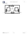
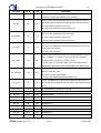
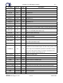
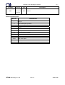
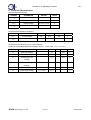
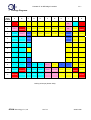
JL4002A
CF to IDE Bridge Controller
Revision: 1.1
Date: 10/26/2004
JEILIN Technology Co., Ltd.
8F, No.179, Jian Yi Rd., Chung Ho,
Taipei Hsien, Taiwan
TEL:886-2-82215466
FAX:886-2-82215456
JL4002A CF to IDE Bridge Controller
V1.1
Table of Contents
0.
REVISION HISTORY................................................................................................................3
1.
GENERAL DESCRIPTION......................................................................................................4
2.
FEATURES ................................................................................................................................4
3.
APPLICATIONS ........................................................................................................................4
4.
BLOCK DIAGRAM ...................................................................................................................5
5.
PIN DESCRIPTIONS................................................................................................................6
6.
ELECTRICAL CHARACTERISTICS ................................................................................... 11
7.
PACKAGE DIAGRAMS .........................................................................................................12
JEILIN Technology Co., Ltd.
2 of 14
2004/10/26
JL4002A CF to IDE Bridge Controller
V1.1
0. Revision History
Revision
Description of Changes
Date
1.0
First Release
2004/1/13
1.1
Change register description
2004/10/26
JEILIN Technology Co., Ltd.
3 of 14
2004/10/26
JL4002A CF to IDE Bridge Controller
V1.1
1. General Description
The JL4002A is a highly-compatible, low cost CF to ATA disk interface (IDE) bridge controller, which
integrates CF interface, IDE interface, and 3-wire serial interface for device controller can download CIS
data CIS RAM. In True-IDE mode, it can support PIO mode up to mode 4, Multiword DMA up to mode 2,
and Ultra DMA mode up to mode 4 transfer.
2. Features
Compliant with CF+ and Compact Flash Specification Revision 3.0
Support all CF modes: Memory, Contiguous IO, Primary IO, Secondary IO, and True IDE modes
Support PIO Mode 4 in True IDE mode
Support Multiword DMA Mode 2 in True IDE mode
Support Ultra DMA Mode 4 in True IDE mode
Support 8-bit/16-bit data transfer on CF data bus & 16-bit access on IDE data bus
Compliant with ATA/ATAPI-6 Specification
Special serial interface to be controlled by device controller
Embedded Task-File registers are provided for host accessing and device controller checking
Embedded internal 256 bytes of CIS RAM
Built-in oscillator circuit using external 20 Mhz crystal
Embedded PLL
Support power saving function for device
Dual clock outputs (1x and 0.5x of crystal frequency)
3.3V, 96 Flip-chip package
3. Applications
Compact-Flash+ Type II Micro-drive Card
IDE/Compact-Flash Adapter
JEILIN Technology Co., Ltd.
4 of 14
2004/10/26
JL4002A CF to IDE Bridge Controller
V1.1
4. Block Diagram
RAM
SIO
IDE Interface
CF Interface
Host (CF)
JEILIN Technology Co., Ltd.
Data Path
5 of 14
IDE
device
2004/10/26
JL4002A CF to IDE Bridge Controller
V1.1
5. Pin Descriptions
Pin Name
Pin No.
Type
Description
Memory mode: CF Address bit 0
CF_A0
E2
I
I/O mode: CF Address bit 0
True IDE mode: CF Address bit 0
Memory mode: CF Address bit 1
CF_A1
F2
I
I/O mode: CF Address bit 1
True IDE mode: CF Address bit 1
Memory mode: CF Address bit 2
CF_A2
G1
I
I/O mode: CF Address bit 2
True IDE mode: CF Address bit 2
Memory mode: CF Address bit 3
CF_A3
H1
I
CF_A4
H2
I
CF_A5
I7
I
CF_A6
J7
I
CF_A7
J6
I
CF_A8
J5
I
CF_A9
I5
I
CF_A10
J3
I
CF_D0
E3
B8
CF Data bit 0
CF_D1
D2
B8
CF Data bit 1
CF_D2
D3
B8
CF Data bit 2
CF_D3
G9
B8
CF Data bit 3
CF_D4
I11
B8
CF Data bit 4
CF_D5
J11
B8
CF Data bit 5
CF_D6
J9
B8
CF Data bit 6
CF_D7
J8
B8
CF Data bit 7
CF_D8
D1
B8
CF Data bit 8
JEILIN Technology Co., Ltd.
I/O mode: CF Address bit 3
Memory mode: CF Address bit 4
I/O mode: CF Address bit 4
Memory mode: CF Address bit 5
I/O mode: CF Address bit 5
Memory mode: CF Address bit 6
I/O mode: CF Address bit 6
Memory mode: CF Address bit 7
I/O mode: CF Address bit 7
Memory mode: CF Address bit 8
I/O mode: CF Address bit 8
Memory mode: CF Address bit 9
I/O mode: CF Address bit 9
Memory mode: CF Address bit 10I/O mode: CF Address bit 10
6 of 14
2004/10/26
JL4002A CF to IDE Bridge Controller
Pin Name
Pin No.
Type
CF_D9
C1
B8
CF Data bit 9
CF_D10
C2
B8
CF Data bit 10
CF_D11
H11
B8
CF Data bit 11
CF_D12
H10
B8
CF Data bit 12
CF_D13
I10
B8
CF Data bit 13
CF_D14
K10
B8
CF Data bit 14
CF_D15
K9
B8
CF Data bit 15
V1.1
Description
Memory mode: CF Card Enable (-CE1)
/CF_CS0
I8
I, U
I/O mode: CF Card Enable (-CE1)
True IDE mode: chip select for the task file registers
Memory mode: CF Card Enable (-CE2)
/CF_CS1
K8
I, U
I/O mode: CF Card Enable (-CE2)
True IDE mode: It is used to select the Alternate Status Register
and the Device Control Register
Memory mode: CF write strobe
/CF_WE
K5
I, U
I/O mode: CF write strobe
True IDE mode: It is not used and should be connected to VCC by
the host.
Memory mode: It is used to read data from CF card of CF+ card in
memory mode and to read the CIS and configuration registers.
/CF_OE
J4
I, U
I/O mode: It is used to read CIS and configuration registers.
True IDE mode: To enable True IDE mode this signal should be
grounded by the host.
Memory mode: not used.
/CF_IOWR
K4
I, U
I/O mode: CF IO write strobe.
True IDE mode: CF IO write strobe (non-Ultra DMA mode) or
STOP (Ultra DMA mode).
Memory mode: not used.
/CF_IORD
K3
I, U
I/O mode: CF IO read strobe.
True IDE mode: CF IO read strobe (non-Ultra DMA mode) or
/HDMARDY (Ultra DMA mode) or HSTROBE (Ultra DMA mode)
CF Write protect (Memory mode) or -IOCS16 (I/O, True IDE mode)
Memory mode: CF Write protect.
CF_WII
J2
O8, T
I/O mode: It is used for the –I/O selected is 16 bit port (-IOIS16)
function. A low signal indicates that a 16 bit or odd byte only
operation can be performed at the addressed port.
JEILIN Technology Co., Ltd.
7 of 14
2004/10/26
JL4002A CF to IDE Bridge Controller
Pin Name
Pin No.
Type
V1.1
Description
True IDE mode: This output signal is asserted low when this device
is expecting a word data transfer cycle (-IOIS16).
Memory mode: It is set high when the card is ready to accept a
CF_RII
K6
O4, T
new data transfer operation and held low when the card is busy.
I/O mode: Interrupt request, active low
True IDE mode: Interrupt request, active high
CF Hardware Reset
CF_RESET
H3
I, U
Memory mode: Hardware Reset, active high
I/O mode: Hardware Reset, active high
True IDE mode: Hardware Reset, active low
Memory mode: Attribute memory select
/CF_REG
F3
I, U
I/O mode: This signal must be active (low) during I/O cycles when
I/O address is on the bus.
True IDE mode: Not used
Memory mode: It is driven to low by the card to signal the host to
delay completion of a memory or I/O cycle that is in progress.
/CF_WAIT
G3
O4, T
I/O mode: Same function as in memory mode.
True IDE mode: It is used as IORDY (non-Ultra DMA mode) or
/DDMARDY (Ultra DMA mode) or DSTROBE (Ultra DMA mode).
CF input acknowledge
/CF_INPACK
G2
O4, T
Memory mode: Not used
I/O mode: CF input acknowledge
True IDE mode: DMA request (Ultra DMA mode)
The CF card detect pin is connected to ground on the card. It is
/CF_CD0
B1
O4, T
used by the host to determine that the card is fully inserted into its
socket.
/CF_CD1
C6
O4, T
CF card detection, same as /CF_CD0 pin
IDE_A0
B5
O4, T
IDE Address bit 0
IDE_A1
C5
O4, T
IDE Address bit 1
IDE_A2
A4
O4, T
IDE Address bit 2
IDE_D0
A7
B4
IDE Data bit 0
IDE_D1
A8
B4
IDE Data bit 1
IDE_D2
B9
B4
IDE Data bit 2
IDE_D3
D9
B4
IDE Data bit 3
IDE_D4
A10
B4
IDE Data bit 4
IDE_D5
B11
B4
IDE Data bit 5
JEILIN Technology Co., Ltd.
8 of 14
2004/10/26
JL4002A CF to IDE Bridge Controller
Pin Name
Pin No.
Type
IDE_D6
D10
B4
IDE Data bit 6
IDE_D7
E11
B4
IDE Data bit 7
IDE_D8
D11
B4
IDE Data bit 8
IDE_D9
C11
B4
IDE Data bit 9
IDE_D10
C10
B4
IDE Data bit 10
IDE_D11
E10
B4
IDE Data bit 11
IDE_D12
A9
B4
IDE Data bit 12
IDE_D13
B8
B4
IDE Data bit 13
IDE_D14
C7
B4
IDE Data bit 14
IDE_D15
B7
B4
IDE Data bit 15
/IDE_IOW
A6
O4, T
/IDE_IOR
B6
O4, T
IDE_IRQ
A5
I, D
Interrupt request, active high
/IDE_RESET
E9
O4, T
Hardware Reset, active low
/IDE_DMACK
B4
O4
IDE_DMARQ
A3
I
IDE_IORDY
J1
I, U
/PORST
F10
I, U
V1.1
Description
IO write strobe (non-Ultra DMA mode) or STOP (Ultra DMA mode)
IO read strobe (non-Ultra DMA mode) or /HDMARDY (Ultra DMA
mode) or HSTROBE (Ultra DMA mode)
DMA acknowledge
DMA request
IORDY (non-Ultra DMA mode) or /DDMARDY (Ultra DMA mode) or
DSTROBE (Ultra DMA mode)
Power on reset
This signal will be set when /PORST signal is active or when a
command is received while bridge is in power saving mode. It will
POWERON
G11
O4
remain High until commanded by the device controller via serial
bus to set to low (power saving). It is used to indicate this chip
whether it is in power saving mode or not.
SIO_ENABLE
F11
I
Serial port enable signal
SIO_CLK
F9
I
Serial clock
SIO_DATA
G10
B4
PXIN
A2
ICLK
Crystal terminal or oscillator input
PXOUT
B3
OCLK
Crystal terminal
CLKOUT_20MHz
I2
O4, T
Clock output. Its clock rate is the same as the clock rate of PXIN.
CLKOUT_10MHz
I1
O4, T
Clock output. Its clock rate is a half of the clock rate of PXIN.
MFG
E1
O2, T
Test pin
TEST_0
F1
I
Test pin
VDD
C3,C8,H9,I4
PWR
+3.3V core power
VCCIO
C4,C9,I3,I9
PWR
+3.3V I/O power
JEILIN Technology Co., Ltd.
serial data line
9 of 14
2004/10/26
JL4002A CF to IDE Bridge Controller
Pin Name
Pin No.
Type
V1.1
Description
A1,A11,B2,
GND
B10,J10, K1,
GND
Ground
K2, K11
Buffer Type Descriptions
BUFFER
DESCRIPTION
I
Input pin
U
Internal weak pull-up resistor
D
Internal weak pull-down resistor
T
Tri-state
B4
Bi-drectional pin with 4 mA drive
B8
Input/output with 8 mA drive
O4
Output pin with 4 mA drive
O8
Output pin with 8 mA drive
ICLK
XTAL clock input
OCLK
XTAL clock output
PWR
Power pin
GND
Ground pin
JEILIN Technology Co., Ltd.
10 of 14
2004/10/26
JL4002A CF to IDE Bridge Controller
V1.1
6. Electrical Characteristics
Absolute Maximum Ratings
SYMBOL
PARAMETER
RATING
UNITS
VCC
Power Supply
-0.3 to 3.6
V
VIN
Input Voltage
-0.3 to VCC+0.3
V
VOUT
Output Voltage
-0.3 to VCC+0.3
V
TSTG
Storage Temperature
-55 to 150
℃
Recommended Operation Conditions
SYMBOL
PARAMETER
MIN
TYP
MAX
UNITS
VCC
Power Supply
3.0
3.3
3.6
V
TOPR
Operating Temperature
0
25
70
℃
DC Electrical Characteristics for 3.3 volts operation
(Under Recommended Operating Conditions and VCC = 3.0V~3.6V, Tj = 0℃ to +70℃)
SYMBOL
PARAMETER
VIL
Input Low Voltage
VIH
VT-
CONDITIONS
MIN
TYP
MAX
UNITS
-0.3
0.8
V
Input High Voltage
2.0
Vcc+0.3
V
Schmitt Input Low
-0.3
0.8
V
2.0
Vcc+0.3
V
0.4
V
Voltage
VT+
Schmitt Input High
Voltage
VOL
Output Low Voltage
IOUT= -4mA
VOH
Output High Voltage
IOUT= 4mA
JEILIN Technology Co., Ltd.
11 of 14
2.4
V
2004/10/26
JL4002A CF to IDE Bridge Controller
V1.1
7. Package Diagrams
Ball
Pitch
310um
A
B
C
D
E
F
G
H
I
J
K
1
GND
/CF_CD0
CF_D9
CF_D8
MFG
TEST_0
CF_A2
CF_A 3
CLKOUT_10
MHZ
IDE_IORDY
GND
2
PXIN
GND
CF_D10
CF_D1
CF_A0
CF_A1
/CF_INPACK
CF_A 4
CLKOUT_20
MHZ
CF_WII
GND
3
IDE_DMARQ
PXOUT
VDD
CF_D2
CF_D0
/CF_REG
/CF_WAIT
CF_RESET
VCCIO
CF_A 10
/CF_IORD
4
IDE_A2
/IDE_DMACK
VCCIO
VDD
/CF_OE
/CF_IOWR
5
IDE_IRQ
IDE_A0
IDE_A1
CF_A 9
CF_A 8
/CF_WE
6
/IDE_IOW
/IDE_IOR
/CF_CD1
N.C.
CF_A 7
CF_RII
7
IDE_D0
IDE_D15
IDE_D14
CF_A 5
CF_A 6
N.C.
8
IDE_D1
IDE_D13
VDD
CF_CS0
CF_D7
CF_CS1
9
IDE_D12
IDE_D2
VCCIO
IDE_D3
/IDE_RESET
SIO_CLK
CF_D3
VDD
VCCIO
CF_D6
CF_D15
10
IDE_D4
GND
IDE_D10
IDE_D6
IDE_D11
/PORST
SIO_DATA
CF_D12
CF_D13
GND
CF_D14
11
GND
IDE_D5
IDE_D9
IDE_D8
IDE_D7
SIO_ENABLE
POWERON
CF_D11
CF_D4
CF_D5
GND
Looking at bumps (bottom side).
JEILIN Technology Co., Ltd.
12 of 14
2004/10/26
JL4002A CF to IDE Bridge Controller
V1.1
A1
JEILIN Technology Co., Ltd.
13 of 14
2004/10/26
JL4002A CF to IDE Bridge Controller
V1.1
JEILIN Technology Co., Ltd.
8F, No. 179, Jian Yi Rd., Chung Ho,
Taipei Hsien, Taiwan
Tel: 886-2-8221-5466
Fax: 886-2-8221-5456
Website: www.jeilin.com.tw
Email: [email protected]
©2005 JEILIN Technology Corp., Ltd. All rights reserved.
The information in this document has been carefully checked and is believed to be reliable;
however no responsibility can be assumed for inaccuracies that may not have been caught. All
information in this document is subject to change without prior notice. The information
contained in this document is presented only as a guide for applications of our products. No
responsibility is assumed by JEILIN Technology for any infringements of intellectual property or
other rights of the third parties, which may result from its use. No license is granted by
implication or otherwise under any intellectual property or other rights of JEILIN Technology or
others. No part of this document may be reproduced in any form, in an electronic retrieval
system or otherwise, without the prior written permission of JEILIN Technology.
JEILIN Technology Co., Ltd.
14 of 14
2004/10/26