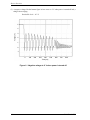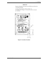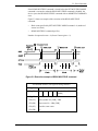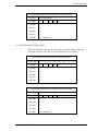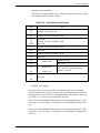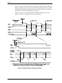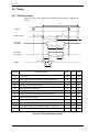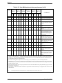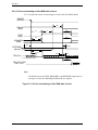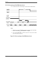
1
C141-E195-02EN MHT2080AH, MHT2060AH, MHT2040AH DISK DRIVES PRODUCT MANUAL FOR SAFE OPERATION Handling of This Manual This manual contains important information for using this product. Read thoroughly before using the product. Use this product only after thoroughly reading and understanding especially the section “Important Alert Items” in this manual. Keep this manual handy, and keep it carefully. FUJITSU makes every effort to prevent users and bystanders from being injured or from suffering damage to their property. Use the product according to this manual. IMPORTANT NOTE TO USERS READ THE ENTIRE MANUAL CAREFULLY BEFORE USING THIS PRODUCT. INCORRECT USE OF THE PRODUCT MAY RESULT IN INJURY OR DAMAGE TO USERS, BYSTANDERS OR PROPERTY. While FUJITSU has sought to ensure the accuracy of all information in this manual, FUJITSU assumes no liability to any party for any damage caused by any error or omission contained in this manual, its updates or supplements, whether such errors or omissions result from negligence, accident, or any other cause. In addition, FUJITSU assumes no liability with respect to the application or use of any product or system in accordance with the descriptions or instructions contained herein; including any liability for incidental or consequential damages arising therefrom. FUJITSU DISCLAIMS ALL WARRANTIES REGARDING THE INFORMATION CONTAINED HEREIN, WHETHER EXPRESSED, IMPLIED, OR STATUTORY. FUJITSU reserves the right to make changes to any products described herein without further notice and without obligation. This product is designed and manufactured for use in standard applications such as office work, personal devices and household appliances. This product is not intended for special uses (atomic controls, aeronautic or space systems, mass transport vehicle operating controls, medical devices for life support, or weapons firing controls) where particularly high reliability requirements exist, where the pertinent levels of safety are not guaranteed, or where a failure or operational error could threaten a life or cause a physical injury (hereafter referred to as "mission-critical" use). Customers considering the use of these products for mission-critical applications must have safety-assurance measures in place beforehand. Moreover, they are requested to consult our sales representative before embarking on such specialized use. The contents of this manual may be revised without prior notice. The contents of this manual shall not be disclosed in any way or reproduced in any media without the express written permission of Fujitsu Limited. All Rights Reserved, Copyright FUJITSU LIMITED 2003 Revision History (1/1) Edition Date 01 2003-06-20 02 2003-10-28 Revised section (*1) (Added/Deleted/Altered) Details Table 1.2 (Altered) Change of the order No. Table 1.5 (Altered) Change of the acoustic noise specification *1 Section(s) with asterisk (*) refer to the previous edition when those were deleted. C141-E195-02EN This page is intentionally left blank. Preface This manual describes about MHT2080AH/MHT2060AH/MHT2040AH out of the disk drive, 2.5-inch hard disk drives. These drives have a built-in controller that is compatible with the ATA interface. This manual describes the specifications and functions of the drives and explains in detail how to incorporate the drives into user systems. This manual assumes that the reader has a basic knowledge of hard disk drives and their implementations in computer systems. This manual consists of seven chapters and sections explaining the special terminology and abbreviations used in this manual: Overview of Manual CHAPTER 1 Device Overview This chapter gives an overview of the disk drive and describes their features. CHAPTER 2 Device Configuration This chapter describes the internal configurations of the disk drive and the configuration of the systems in which they operate. CHAPTER 3 Installation Conditions This chapter describes the external dimensions, installation conditions, and switch settings of the disk drive. CHAPTER 4 Theory of Device Operation This chapter describes the operation theory of the disk drive. CHAPTER 5 Interface This chapter describes the interface specifications of the disk drive. CHAPTER 6 Operations This chapter describes the operations of the disk drive. Glossary The glossary describes the technical terms that need to be understood to read this manual. Acronyms and Abbreviations This section gives the meanings of the definitions used in this manual. C141-E195-02EN i Preface Conventions for Alert Messages This manual uses the following conventions to show the alert messages. An alert message consists of an alert signal and alert statements. The alert signal consists of an alert symbol and a signal word or just a signal word. The following are the alert signals and their meanings: This indicates a hazardous situation could result in minor or moderate personal injury if the user does not perform the procedure correctly. This alert signal also indicates that damages to the product or other property may occur if the user does not perform the procedure correctly. This indicates information that could help the user use the product more efficiently. In the text, the alert signal is centered, followed below by the indented message. A wider line space precedes and follows the alert message to show where the alert message begins and ends. The following is an example: (Example) Data corruption: Avoid mounting the disk drive near strong magnetic sources such as loud speakers. Ensure that the disk drive is not affected by external magnetic fields. The main alert messages in the text are also listed in the “Important Alert Items.” Operating Environment This product is designed to be used in offices or computer rooms. Conventions An disk drive device is sometimes simply referred to as a "hard disk drive," "HDD," "drive," or "device" in this document. Decimal numbers are represented normally. Hexadecimal numbers are represented as shown in the following examples: X'17B9', 17B9h, 17B9H, or 17B9H. Binary numbers are represented as shown in the following examples: 010 or 010b. ii C141-E195-02EN Preface Attention Please forward any comments you may have regarding this manual. To make this manual easier for users to understand, opinions from readers are needed. Please write your opinions or requests on the Comment at the back of this manual and forward it to the address described in the sheet. Liability Exception “Disk drive defects” refers to defects that involve adjustment, repair, or replacement. Fujitsu is not liable for any other disk drive defects, such as those caused by user misoperation or mishandling, inappropriate operating environments, defects in the power supply or cable, problems of the host system, or other causes outside the disk drive. C141-E195-02EN iii This page is intentionally left blank. Important Alert Items Important Alert Messages The important alert messages in this manual are as follows: A hazardous situation could result in minor or moderate personal injury if the user does not perform the procedure correctly. Also, damage to the product or other property, may occur if the user does not perform the procedure correctly. Task Normal Operation Alert message Page Data corruption: Avoid mounting the disk near strong magnetic sources such as loud speakers. Ensure that the disk drive is not affected by external magnetic fields. Damage: Do not press the cover of the disk drive. Pressing it too hard, the cover and the spindle motor contact, which may cause damage to the disk drive. 3-7 Static: When handling the device, disconnect the body ground (500 kΩ or greater). Do not touch the printed circuit board, but hold it by the edges. C141-E195-02EN v This page is intentionally left blank. Manual Organization MHT2080AH, MHT2060AH, MHT2040AH DISK DRIVES PRODUCT MANUAL (C141-E195) • • • • • • Device Overview Device Configuration Installation Conditions Theory of Device Operation Interface Operations <This manual> MHT2080AH, MHT2060AH, MHT2040AH • Maintenance and Diagnosis • Removal and Replacement Procedure DISK DRIVES MAINTENANCE MANUAL (C141-F065) C141-E195-02EN vii This page is intentionally left blank. Contents CHAPTER 1 Device Overview ........................................................................ 1-1 1.1 Features ...................................................................................................1-2 1.1.1 Functions and performance ...................................................................1-2 1.1.2 Adaptability...........................................................................................1-2 1.1.3 Interface.................................................................................................1-3 1.2 Device Specifications..............................................................................1-4 1.2.1 Specifications summary ........................................................................1-4 1.2.2 Model and product number ...................................................................1-5 1.3 Power Requirements ...............................................................................1-5 1.4 Environmental Specifications .................................................................1-8 1.5 Acoustic Noise ........................................................................................1-9 1.6 Shock and Vibration................................................................................1-9 1.7 Reliability..............................................................................................1-10 1.8 Error Rate ..............................................................................................1-11 1.9 Media Defects .......................................................................................1-11 1.10 Load/Unload Function ..........................................................................1-11 1.11 Advanced Power Management..............................................................1-12 CHAPTER 2 C141-E195-02EN Device Configuration ................................................................ 2-1 2.1 Device Configuration ..............................................................................2-2 2.2 System Configuration..............................................................................2-3 2.2.1 ATA interface .......................................................................................2-3 2.2.2 1 drive connection .................................................................................2-3 2.2.3 2 drives connection ...............................................................................2-4 ix Contents CHAPTER 3 Installation Conditions ............................................................. 3-1 3.1 Dimensions ..............................................................................................3-2 3.2 Mounting .................................................................................................3-3 3.3 Cable Connections...................................................................................3-9 3.3.1 Device connector ...................................................................................3-9 3.3.2 Cable connector specifications............................................................3-10 3.3.3 Device connection ...............................................................................3-10 3.3.4 Power supply connector (CN1) ...........................................................3-10 3.4 CHAPTER 4 3.4.1 Location of setting jumpers.................................................................3-11 3.4.2 Factory default setting.........................................................................3-12 3.4.3 Master drive-slave drive setting ..........................................................3-12 3.4.4 CSEL setting........................................................................................3-13 3.4.5 Power Up in Standby setting ...............................................................3-14 Theory of Device Operation ..................................................... 4-1 4.1 Outline .....................................................................................................4-2 4.2 Subassemblies..........................................................................................4-2 4.2.1 Disk........................................................................................................4-2 4.2.2 Spindle...................................................................................................4-2 4.2.3 Actuator .................................................................................................4-2 4.2.4 Air filter.................................................................................................4-3 4.3 Circuit Configuration ..............................................................................4-3 4.4 Power-on Sequence .................................................................................4-6 4.5 Self-calibration ........................................................................................4-7 4.5.1 Self-calibration contents........................................................................4-7 4.5.2 Execution timing of self-calibration......................................................4-8 4.5.3 Command processing during self-calibration........................................4-8 4.6 4.6.1 x Jumper Settings .....................................................................................3-11 Read/write Circuit ...................................................................................4-9 Read/write preamplifier (PreAMP) .......................................................4-9 C141-E195-02EN Contents 4.6.2 Write circuit ..........................................................................................4-9 4.6.3 Read circuit .........................................................................................4-10 4.6.4 Digital PLL circuit ..............................................................................4-11 4.7 CHAPTER 5 4.7.1 Servo control circuit............................................................................4-12 4.7.2 Data-surface servo format ...................................................................4-14 4.7.3 Servo frame format..............................................................................4-16 4.7.4 Actuator motor control........................................................................4-17 4.7.5 Spindle motor control..........................................................................4-18 Interface ..................................................................................... 5-1 5.1 Physical Interface ....................................................................................5-2 5.1.1 Interface signals ....................................................................................5-2 5.1.2 Signal assignment on the connector......................................................5-3 5.2 Logical Interface .....................................................................................5-6 5.2.1 I/O registers ...........................................................................................5-7 5.2.2 Command block registers......................................................................5-8 5.2.3 Control block registers ........................................................................5-13 5.3 Host Commands ....................................................................................5-14 5.3.1 Command code and parameters ..........................................................5-14 5.3.2 Command descriptions........................................................................5-18 5.3.3 Error posting......................................................................................5-107 5.4 Command Protocol..............................................................................5-109 5.4.1 PIO Data transferring commands from device to host ......................5-109 5.4.2 PIO Data transferring commands from host to device......................5-112 5.4.3 Commands without data transfer ......................................................5-114 5.4.4 Other commands ...............................................................................5-115 5.4.5 DMA data transfer commands ..........................................................5-115 5.5 C141-E195-02EN Servo Control ........................................................................................4-12 Ultra DMA Feature Set .......................................................................5-118 5.5.1 Overview ...........................................................................................5-118 5.5.2 Phases of operation ...........................................................................5-119 5.5.3 Ultra DMA data in commands ..........................................................5-119 xi Contents 5.5.3.1 Initiating an Ultra DMA data in burst .............................................5-119 5.5.3.2 The data in transfer..........................................................................5-120 5.5.3.3 Pausing an Ultra DMA data in burst ...............................................5-120 5.5.3.4 Terminating an Ultra DMA data in burst ........................................5-121 5.5.4 Ultra DMA data out commands ........................................................5-124 5.5.4.1 Initiating an Ultra DMA data out burst ...........................................5-124 5.5.4.2 The data out transfer........................................................................5-124 5.5.4.3 Pausing an Ultra DMA data out burst .............................................5-125 5.5.4.4 Terminating an Ultra DMA data out burst ......................................5-126 5.5.5 Ultra DMA CRC rules.......................................................................5-128 5.5.6 Series termination required for Ultra DMA ......................................5-129 5.6 Timing .................................................................................................5-130 5.6.1 PIO data transfer................................................................................5-130 5.6.2 Multiword data transfer.....................................................................5-131 5.6.3 Ultra DMA data transfer ...................................................................5-132 5.6.3.1 Initiating an Ultra DMA data in burst .............................................5-132 5.6.3.2 Ultra DMA data burst timing requirements ....................................5-133 5.6.3.3 Sustained Ultra DMA data in burst .................................................5-136 5.6.3.4 Host pausing an Ultra DMA data in burst.......................................5-137 5.6.3.5 Device terminating an Ultra DMA data in burst .............................5-138 5.6.3.6 Host terminating an Ultra DMA data in burst.................................5-139 5.6.3.7 Initiating an Ultra DMA data out burst ...........................................5-140 5.6.3.8 Sustained Ultra DMA data out burst ...............................................5-141 5.6.3.9 Device pausing an Ultra DMA data out burst .................................5-142 5.6.3.10 Host terminating an Ultra DMA data out burst...............................5-143 5.6.3.11 Device terminating an Ultra DMA data out burst ...........................5-144 5.6.4 CHAPTER 6 Operations ................................................................................. 6-1 6.1 xii Power-on and reset ............................................................................5-145 Device Response to the Reset .................................................................6-2 6.1.1 Response to power-on ...........................................................................6-2 6.1.2 Response to hardware reset ...................................................................6-3 6.1.3 Response to software reset ....................................................................6-5 6.1.4 Response to diagnostic command .........................................................6-6 C141-E195-02EN Contents 6.2 Power Save..............................................................................................6-7 6.2.1 Power save mode...................................................................................6-7 6.2.2 Power commands ..................................................................................6-9 6.3 Defect Processing....................................................................................6-9 6.3.1 Spare area ..............................................................................................6-9 6.3.2 Alternating processing for defective sectors.......................................6-10 6.4 Read-ahead Cache .................................................................................6-12 6.4.1 DATA buffer structure........................................................................6-12 6.4.2 Caching operation ...............................................................................6-13 6.4.3 Using the read segment buffer ............................................................6-15 6.4.3.1 Miss-hit .............................................................................................6-15 6.4.3.2 Sequential Hit....................................................................................6-16 6.4.3.3 Full hit ...............................................................................................6-17 6.4.3.4 Partial hit ...........................................................................................6-18 6.5 6.5.1 Write Cache...........................................................................................6-19 Cache operation...................................................................................6-19 Glossary ........................................................................................................... GL-1 Acronyms and Abbreviations ......................................................................... AB-1 Index ................................................................................................................. IN-1 C141-E195-02EN xiii Contents Illustrations Figures xiv Figure 1.1 Figure 1.2 Negative voltage at +5 V when power is turned off ..........................1-6 Current fluctuation (Typ.) at +5 V when power is turned on ............1-8 Figure 2.1 Figure 2.2 Figure 2.3 Disk drive outerview ..........................................................................2-2 1 drive system configuration ..............................................................2-3 2 drives configuration.........................................................................2-4 Figure 3.1 Figure 3.2 Figure 3.3 Figure 3.4 Figure 3.5 Figure 3.6 Figure 3.7 Figure 3.8 Figure 3.9 Figure 3.10 Figure 3.11 Figure 3.12 Figure 3.13 Figure 3.14 Figure 3.15 Figure 3.16 Dimensions.........................................................................................3-2 Orientation..........................................................................................3-3 Mounting frame structure...................................................................3-4 Location of breather ...........................................................................3-5 Surface temperature measurement points ..........................................3-6 Service area ........................................................................................3-7 Handling cautions...............................................................................3-8 Connector locations............................................................................3-9 Cable connections ............................................................................3-10 Power supply connector pins (CN1) ................................................3-11 Jumper location ................................................................................3-11 Factory default setting......................................................................3-12 Jumper setting of master or slave drive............................................3-12 CSEL setting.....................................................................................3-13 Example (1) of Cable Select.............................................................3-13 Example (2) of Cable Select.............................................................3-14 Figure 4.1 Figure 4.2 Figure 4.3 Figure 4.4 Figure 4.5 Figure 4.6 Figure 4.7 Figure 4.8 Power Supply Configuration ..............................................................4-4 Circuit Configuration .........................................................................4-5 Power-on operation sequence.............................................................4-6 Read/write circuit block diagram .......................................................4-9 Frequency characteristic of programmable filter .............................4-10 Block diagram of servo control circuit.............................................4-12 Physical sector servo configuration on disk surface ........................4-15 Servo frame format...........................................................................4-16 Figure 5.1 Figure 5.2 Figure 5.3 Interface signals..................................................................................5-2 Execution example of READ MULTIPLE command......................5-21 Read Sector(s) command protocol .................................................5-110 C141-E195-02EN Contents Figure 5.4 Figure 5.5 Figure 5.6 Figure 5.7 Figure 5.8 Figure 5.9 Figure 5.10 Figure 5.11 Figure 5.12 Figure 5.13 Figure 5.14 Figure 5.15 Figure 5.16 Figure 5.17 Figure 5.18 Figure 5.19 Figure 5.20 Figure 5.21 Protocol for command abort ..........................................................5-111 WRITE SECTOR(S) command protocol.......................................5-113 Protocol for the command execution without data transfer ...........5-114 Normal DMA data transfer ............................................................5-117 Ultra DMA termination with pull-up or pull-down .......................5-129 PIO data transfer timing.................................................................5-130 Multiword DMA data transfer timing (mode 2) ............................5-131 Initiating an Ultra DMA data in burst............................................5-132 Sustained Ultra DMA data in burst................................................5-136 Host pausing an Ultra DMA data in burst .....................................5-137 Device terminating an Ultra DMA data in burst............................5-138 Host terminating an Ultra DMA data in burst ...............................5-139 Initiating an Ultra DMA data out burst..........................................5-140 Sustained Ultra DMA data out burst..............................................5-141 Device pausing an Ultra DMA data out burst................................5-142 Host terminating an Ultra DMA data out burst .............................5-143 Device terminating an Ultra DMA data out burst..........................5-144 Power-on Reset Timing..................................................................5-145 Figure 6.1 Figure 6.2 Figure 6.3 Figure 6.4 Figure 6.5 Figure 6.6 Figure 6.7 Response to power-on ........................................................................6-3 Response to hardware reset................................................................6-4 Response to software reset.................................................................6-5 Response to diagnostic command ......................................................6-6 Sector slip processing ......................................................................6-10 Automatic alternating processing.....................................................6-11 Data buffer structure ........................................................................6-12 C141-E195-02EN xv Contents Tables Table 1.1 Table 1.2 Table 1.3 Table 1.4 Table 1.5 Table 1.6 Specifications .....................................................................................1-4 Model names and product numbers.....................................................1-5 Current and power dissipation ............................................................1-7 Environmental specifications ..............................................................1-8 Acoustic noise specification................................................................1-9 Shock and vibration specification .......................................................1-9 Table 3.1 Table 3.2 Surface temperature measurement points and standard values...........3-6 Cable connector specifications..........................................................3-10 Table 5.1 Signal assignment on the interface connector .....................................5-3 Table 5.2 I/O registers .........................................................................................5-7 Table 5.3 Command code and parameters ........................................................5-15 Table 5.4 Information to be read by IDENTIFY DEVICE command ..............5-34 Table 5.5 Features register values and settable modes......................................5-44 Table 5.6 Diagnostic code .................................................................................5-56 Table 5.7 Features Register values (subcommands) and functions ..................5-68 Table 5.8 Format of device attribute value data................................................5-72 Table 5.9 Format of insurance failure threshold value data..............................5-72 Table 5.10 Log Directory Data Format ..............................................................5-77 Table 5.11 Data format of SMART Summary Error Log ..................................5-78 Table 5.11.1 Data format of SMART Comprehensive Error Log.........................5-79 Table 5.12 SMART self-test log data format .....................................................5-80 Table 5.13 Selective self-test log data structure.................................................5-81 Table 5.14 Selective self-test feature flags.........................................................5-82 Table 5.15 Contents of security password..........................................................5-83 Table 5.16 Contents of SECURITY SET PASSWORD data ............................5-87 Table 5.17 Relationship between combination of Identifier and Security level, and operation of the lock function.....................5-88 Table 5.18 DEVICE CONFIGURATION IDENTIFY data structure................5-94 Table 5.19 Operation of DOWNLOAD MICRO CODE .................................5-106 Table 5.20 Example of rewriting procedure of data 384 KBytes (30000h Bytes) of microcode ........................................................5-106 Table 5.21 Command code and parameters .....................................................5-107 Table 5.22 Recommended series termination for Ultra DMA .........................5-129 Table 5.23 Ultra DMA data burst timing requirements ..................................5-133 Table 5.24 Ultra DMA sender and recipient timing requirements...................5-135 xvi C141-E195-02EN CHAPTER 1 Device Overview 1.1 Features 1.2 Device Specifications 1.3 Power Requirements 1.4 Environmental Specifications 1.5 Acoustic Noise 1.6 Shock and Vibration 1.7 Reliability 1.8 Error Rate 1.9 Media Defects 1.10 Load/Unload Function 1.11 Advanced Power Management Overview and features are described in this chapter, and specifications and power requirement are described. The disk drive is 2.5-inch hard disk drive with built-in disk controllers. These disk drives use the AT-bus hard disk interface protocol and are compact and reliable. C141-E195-02EN 1-1 Device Overview 1.1 Features 1.1.1 Functions and performance The following features of the disk drive is described. (1) Compact The disk drive has 1 disk or 2 disks of 65 mm (2.5 inches) diameter, and its height is 9.5 mm (0.374 inch). (2) Large capacity The disk drive can record up to 40 GB (formatted) on one disk using the 60/63 RLL recording method and 30 recording zone technology. The disk drive has a formatted capacity of 80 GB (MHT2080AH), 60 GB (MHT2060AH), and 40 GB (MHT2040AH) respectively. (3) High-speed Transfer rate The disk drives have an internal data rate up to 55.4 MB/s. The disk drive supports an external data rate up to 100 MB/s (U-DMA mode 5). (4) Average positioning time Use of a rotary voice coil motor in the head positioning mechanism greatly increases the positioning speed. The average positioning time is 12 ms (at read). 1.1.2 Adaptability (1) Power save mode The power save mode feature for idle operation, stand by and sleep modes makes The disk drives ideal for applications where power consumption is a factor. (2) Wide temperature range The disk drives can be used over a wide temperature range (5 °C to 55 °C). (3) Low noise and vibration In Ready status, the noise of the disk drives is only 25 dBA (measured at 0.3 m apart from the drive under the idle mode). (4) High resistance against shock The Load/Unload mechanism is highly resistant against non-operation shock up to 8820 m/s2 (900G). 1-2 C141-E195-02EN 1.1 Features 1.1.3 Interface (1) Connection to ATA interface The disk drives have built-in controllers compatible with the ATA interface. (2) 8 MB data buffer The disk drives use a 8 MB data buffer to transfer data between the host and the disk media. In combination with the read-ahead cache system described in item (3) and the write cache described in item (7), the buffer contributes to efficient I/O processing. (3) Read-ahead cache system After the execution of a disk read command, the disk drive automatically reads the subsequent data block and writes it to the data buffer (read ahead operation). This cache system enables fast data access. The next disk read command would normally cause another disk access. But, if the read ahead data corresponds to the data requested by the next read command, the data in the buffer can be transferred instead. (4) Master/slave The disk drives can be connected to ATA interface as daisy chain configuration. Drive 0 is a master device, drive 1 is a slave device. (5) Error correction and retry by ECC If a recoverable error occurs, the disk drives themselves attempt error recovery. The ECC has improved buffer error correction for correctable data errors. (6) Self-diagnosis The disk drives have a diagnostic function to check operation of the controller and disk drives. Executing a diagnostic function of the smart command invokes selfdiagnosis. (7) Write cache When the disk drives receive a write command, the disk drives post the command completion at completion of transferring data to the data buffer completion of writing to the disk media. This feature reduces the access time at writing. C141-E195-02EN 1-3 Device Overview 1.2 Device Specifications 1.2.1 Specifications summary Table 1.1 shows the specifications of the disk drives. Table 1.1 Specifications (1/2) Format Capacity (*1) Number of Sectors (User) MHT2080AH MHT2060AH MHT2040AH 80 GB 60 GB 40 GB 156,301,488 117,210,240 78,140,160 Bytes per Sector 512 Rotational Speed 5,400 rpm ± 1% Average Latency 5.56 ms Positioning time (read and seek) • Minimum (Track-Track) • Average 1.5 ms (typ.) Read: 12ms (typ.) • Maximum (Full) 22 ms (typ.) Start time 4.0 sec (typ.) Interface ATA-6 (Max. Cable length: 18inches (0.46 m)) (equipped with expansion function) Data Transfer Rate • To/From Media 55.4 MB/s Max. • To/From Host 100 MB/s Max (U-DMA mode5) Data Buffer Size 4 MB Physical Dimensions (Height × Width × Depth) Weight 9.5 mm × 100.0 mm × 70.0 mm 99 g (max) *1: Capacity under the LBA mode. 1-4 C141-E195-02EN 1.3 Power Requirements Table 1.1 lists the formatted capacity, number of logical cylinders, number of heads, and number of sectors of every model for which the CHS mode has been selected using the BIOS setup utility on the host. Table 1.1 Specifications (2/2) Model Capacity (*1) No. of Cylinder No. of Heads No. of Sectors MHT2080AH 8.45 GB 16,383 16 63 MHT2060AH 8.45 GB 16,383 16 63 MHT2040AH 8.45 GB 16,383 16 63 *1 On using for the units of BIOS parameter. 1.2.2 Model and product number Table 1.2 lists the model names and product numbers of the disk drive. Table 1.2 Model names and product numbers Model Name Capacity (user area) Mounting screw MHT2080AH 80 GB M3 depth 3 CA06377-B048 MHT2060AH 60 GB M3 depth 3 CA06377-B046 MHT2040AH 40 GB M3 depth 3 CA06377-B024/(B034) Order No. 1.3 Power Requirements (1) Input Voltage • +5V ±5% (2) Ripple +5 V C141-E195-02EN Maximum 100 mV (peak to peak) Frequency DC to 1 MHz 1-5 Device Overview (3) A negative voltage like the bottom figure isn't to occur at +5 V when power is turned off and, a thing with no ringing. Permissible level: −0.2 V 5 Voltage [V] 4 3 2 1 0 -1 0 100 200 300 400 500 600 700 800 Time [ms] Figure 1.1 Negative voltage at +5 V when power is turned off 1-6 C141-E195-02EN 1.3 Power Requirements (4) Current Requirements and Power Dissipation Table 1.3 lists the current and power dissipation (typical). Table 1.3 Current and power dissipation Typical RMS Current Typical Power (*3) 1.0 A 5.0 W 170 mA 0.85 W Read 460 mA / Write 460mA Read 2.3 W / Write 2.3 W Seek (*5) 500 mA 2.5 W Standby 50 mA 0.25 W Sleep 20 mA 0.1 W Spin up (*1) Idle R/W (on track) (*2) Energy Efficiency (*4) — MHT2080AH (CA06377-B048): rank E 0.011W/GB MHT2060AH (CA06377-B046) : rank E 0.014 W/GB MHT2040AH (CA06377-B034) : rank E 0.021W/GB MHT2040AH (CA06377-B024) : rank D 0.021 W/GB *1 Current at starting spindle motor. *2 Current and power level when the operation (command) that accompanies a transfer of 63 sectors is executed 3 times in 100 ms *3 Power requirements reflect nominal values for +5 V power. *4 Energy efficiency based on the Law concerning the Rational Use of Energy indicates the value obtained by dividing power consumption by the storage capacity. (Japan only) *5 The seek average current is specified based on three operations per 100 msec. (5) Current fluctuation (Typ.) at +5 V when power is turned on C141-E195-02EN 1-7 Device Overview Figure 1.2 Current fluctuation (Typ.) at +5 V when power is turned on (6) Power on/off sequence The voltage detector circuits monitor +5 V. The circuits do not allow a write signal if either voltage is abnormal. These prevent data from being destroyed and eliminates the need to be concerned with the power on/off sequence. 1.4 Environmental Specifications Table 1.4 lists the environmental specifications. Table 1.4 Environmental specifications Item Temperature • Operating • Non-operating • Thermal Gradient Humidity • Operating • Non-operating • Maximum Wet Bulb Altitude (relative to sea level) • Operating • Non-operating 1-8 Specification 5 °C to 55 °C (ambient) 5 °C to 60 °C (disk enclosure surface) –40 °C to 65 °C 20 °C/h or less 8 % to 90 % RH (Non-condensing) 5 % to 95 % RH (Non-condensing) 29 °C (Operating) 40 °C (Non-operating) –300 to 3,000 m –300 to 12,000 m C141-E195-02EN 1.5 Acoustic Noise 1.5 Acoustic Noise Table 1.5 lists the acoustic noise specification. Table 1.5 Acoustic noise specification Item Specification (typ.) • Idle mode (DRIVE READY) 2.2 B [MHT2040AH] Sound Power 2.8 B [MHT2080AH/MHT2060AH/MHT2040AH (*1)] Sound Pressure (at 0.3m) 25 dB(A) [MHT2040AH] 34 dB(A) [MHT2080AH/MHT2060AH/MHT2040AH (*1)] * 1 In case of model “CA06377-B034”. 1.6 Shock and Vibration Table 1.6 lists the shock and vibration specification. Table 1.6 Shock and vibration specification Item Specification Vibration (Swept sine, 1/4 octave per minute) • Operating • Non-operating 5 to 500 Hz, 9.8m/s2 0-peak (1G 0-peak) (without non-recovered errors) 5 to 500 Hz, 49m/s2 0-peak (5G 0-peak) (no damage) Shock (half-sine pulse) • Operating • Non-operating 2207 m/s2 0-peak (225G 0-peak) 2ms duration (without non-recovered errors) 8820 m/s2 0-peak (900G 0-peak) 1ms duration 1176 m/s2 0-peak (120G 0-peak) 11ms duration (no damage) C141-E195-02EN 1-9 Device Overview 1.7 Reliability (1) Mean time between failures (MTBF) Conditions of 300,000 h Power-on time Operating time Environment 250H/month or less 3000H/years or less 20 % or less of power-on time 5 to 55 °C/8 to 90 % But humidity bulb temperature 29 °C or less MTBF is defined as follows: Total operation time in all fields MTBF= (H) number of device failure in all fields (*1) *1 “Disk drive defects” refers to defects that involve repair, readjustment, or replacement. Disk drive defects do not include failures caused by external factors, such as damage caused by handling, inappropriate operating environments, defects in the power supply host system, or interface cable. (2) Mean time to repair (MTTR) The mean time to repair (MTTR) is 30 minutes or less, if repaired by a specialist maintenance staff member. (3) Service life In situations where management and handling are correct, the disk drive requires no overhaul for five years when the DE surface temperature is less than 48 °C. When the DE surface temperature exceeds 48 °C, the disk drives requires no overhaul for five years or 20,000 hours of operation, whichever occurs first. Refer to item (3) in Subsection 3.2 for the measurement point of the DE surface temperature. Also the operating conditions except the environment temperature are based on the MTBF conditions. (4) Data assurance in the event of power failure Except for the data block being written to, the data on the disk media is assured in the event of any power supply abnormalities. This does not include power supply abnormalities during disk media initialization (formatting) or processing of defects (alternative block assignment). 1-10 C141-E195-02EN 1.8 Error Rate 1.8 Error Rate Known defects, for which alternative blocks can be assigned, are not included in the error rate count below. It is assumed that the data blocks to be accessed are evenly distributed on the disk media. (1) Unrecoverable read error Read errors that cannot be recovered by maximum read retries of drive without user’s retry and ECC corrections shall occur no more than 10 times when reading data of 1014 bits. Read retries are executed according to the disk drive’s error recovery procedure, and include read retries accompanying head offset operations. (2) Positioning error Positioning (seek) errors that can be recovered by one retry shall occur no more than 10 times in 107 seek operations. 1.9 Media Defects Defective sectors are replaced with alternates when the disk are formatted prior to shipment from the factory (low level format). Thus, the hosts see a defect-free devices. Alternate sectors are automatically accessed by the disk drive. The user need not be concerned with access to alternate sectors. 1.10 Load/Unload Function The Load/Unload function is a mechanism that loads the head on the disk and unloads the head from the disk. The product supports a minimum of 300,000 normal Load/Unload cycles. Normal Unload is a normal head unloading operation and the commands listed below are executed. • Hard Reset • Standby • Standby immediate • Sleep • Idle Emergency Unload other than Normal Unload is performed when the power is shut down while the heads are still loaded on the disk. The product supports the Emergency Unload a minimum of 20,000 times. When the power is shut down, the controlled Normal Unload cannot be executed. Therefore, the number of Emergency other than Normal Unload is specified. C141-E195-02EN 1-11 Device Overview Remark: We recommend cutting the power supply of the HDD for this device after the Head Unload operation completes. The recommended power supply cutting sequence for this device is as follows: 1) Disk Flush Flush Cache command execution. 2) Head Unload Standby Immediate command execution. 3) Wait Status Checking whether bit 7 of the status register was set to '0'. (wait to complete STANDBY IMMEDIATE command) 4) HDD power supply cutting 1.11 Advanced Power Management The disk drive shifts to the three kinds of APM modes automatically under the Idle condition. The APM mode can be chosen with a Sector Count register of the SET FEATURES(EF) command. In APM Mode-1, which is the APM default mode, the operation status shifts till it finally reaches "Low Power Idle." The disk drive complies with the three kinds of APM modes that a command from the host is required. FR = 05h : Enable APM SC = C0h - FEh : Mode-0 Active Idle → Low Power Idle SC = 80h - BFh : Mode-1 Active Idle → Low Power Idle (Default) SC = 01h - 7Fh : Mode-2 Active Idle → Low Power Idle → Standby FR = 85h : Disable APM (return to Default.) 1-12 C141-E195-02EN 1.11 Advanced Power Management Active Idle: The head is in a position of extreme inner in disk medium. (VCM Lock) Low Power Idle: The head is unloaded from disk. (VCM Unload) The spindle motor rotates. Standby: The spindle motor stops. APM Mode Active Idle (VCM Lock) Low Power Idle (VCM Unload) Standby (Spin Off) Mode-0 0.2-1.2 sec 15 min. N/A Mode-1 0.2-1.2 sec 10.0-40.0 sec N/A Mode-2 0.2-1.2 sec 10.0-40.0 sec 10.0-40.0 sec When the maximum time that the HDD is waiting for commands has been exceeded: Mode-0: Mode shifts from Active condition to Active Idle in 0.2-1.2, and to Low Power Idle in 15 minutes. Mode-1: Mode shifts from Active condition to Active Idle in 0.2-1.2 seconds and to Low Power Idle in 10.0-40.0 seconds. Mode-2: Mode shifts from Active condition to Active Idle in 0.2-1.2 seconds and to Low Power Idle in 10.0-40.0 seconds. After 10.0-40.0 seconds in Low Power Idle, the mode shifts to standby. C141-E195-02EN 1-13 This page is intentionally left blank. CHAPTER 2 Device Configuration 2.1 Device Configuration 2.2 System Configuration This chapter describes the internal configurations of the hard disk drives and the configuration of the systems in which they operate. C141-E195-02EN 2-1 Device Configuration 2.1 Device Configuration Figure 2.1 shows the disk drive. The disk drive consists of a disk enclosure (DE), read/write preamplifier, and controller PCA. The disk enclosure contains the disk media, heads, spindle motors, actuators, and a circulating air filter. Disk drive Figure 2.1 Disk drive outerview (1) Disk The outer diameter of the disk is 65 mm. The inner diameter is 20 mm. (2) Head The heads are of the load/unload (L/UL) type. The head unloads the disk out of while the disk is not rotating and loads on the disk when the disk starts. (3) Spindle motor The disks are rotated by a direct drive Sensor-less DC motor. (4) Actuator The actuator uses a revolving voice coil motor (VCM) structure which consumes low power and generates very little heat. The head assembly at the edge of the actuator arm is controlled and positioned by feedback of the servo information read by the read/write head. If the power is not on or if the spindle motor is stopped, the head assembly stays on the ramp out of the disk and is fixed by a mechanical lock. (5) Air circulation system The disk enclosure (DE) is sealed to prevent dust and dirt from entering. The disk enclosure features a closed loop air circulation system that relies on the blower effect of the rotating disk. This system continuously circulates the air through the circulation filter to maintain the cleanliness of the air within the disk enclosure. 2-2 C141-E195-02EN 2.2 System Configuration (6) Read/write circuit The read/write circuit uses a LSI chip for the read/write preamplifier. It improves data reliability by preventing errors caused by external noise. (7) Controller circuit The controller circuit consists of an LSI chip to improve reliability. The highspeed microprocessor unit (MPU) achieves a high-performance AT controller. 2.2 System Configuration 2.2.1 ATA interface Figures 2.2 and 2.3 show the ATA interface system configuration. The drive has a 44pin PC AT interface connector and supports PIO mode 4 transfer at 16.6 MB/s, Multiword DMA mode 2 transfer at 16.6 MB/s and also U-DMA mode 5 (100 MB/s). 2.2.2 1 drive connection MHT2080AH MHC2032AT MHT2060AH MHC2040AT MHT2040AH Figure 2.2 1 drive system configuration C141-E195-02EN 2-3 Device Configuration 2.2.3 2 drives connection (Host adaptor) MHT2080AH MHT2060AH MHC2032AT MHC2040AT MHT2040AH MHT2080AH MHC2032AT MHT2060AH MHC2040AT MHT2040AH Note: When the drive that is not conformed to ATA is connected to the disk drive above configuration, the operation is not guaranteed. Figure 2.3 2 drives configuration IMPORTANT HA (host adaptor) consists of address decoder, driver, and receiver. ATA is an abbreviation of “AT attachment”. The disk drive is conformed to the ATA-6 interface. At high speed data transfer (PIO mode 4 or DMA mode 2 U-DMA mode 5), occurrence of ringing or crosstalk of the signal lines (AT bus) between the HA and the disk drive may be a great cause of the obstruction of system reliability. Thus, it is necessary that the capacitance of the signal lines including the HA and cable does not exceed the ATA-6 standard, and the cable length between the HA and the disk drive should be as short as possible. No need to push the top cover of the disk drive. If the over-power worked, the cover could be contacted with the spindle motor. Thus, that could be made it the cause of failure. 2-4 C141-E195-02EN CHAPTER 3 Installation Conditions 3.1 Dimensions 3.2 Mounting 3.3 Cable Connections 3.4 Jumper Settings This chapter gives the external dimensions, installation conditions, surface temperature conditions, cable connections, and switch settings of the hard disk drives. For information about handling this hard disk drive and the system installation procedure, refer to the following Integration Guide. C141-E144 C141-E195-02EN 3-1 Installation Conditions 3.1 Dimensions Figure 3.1 illustrates the dimensions of the disk drive and positions of the mounting screw holes. All dimensions are in mm. Figure 3.1 Dimensions 3-2 C141-E195-02EN 3.2 Mounting 3.2 Mounting For information on mounting, see the "FUJITSU 2.5-INCH HDD INTEGRATION GUIDANCE (C141-E144)." (1) Orientation Figure 3.2 illustrates the allowable orientations for the disk drive. gravity (a) Horizontal –1 (b) Horizontal –1 gravity (d) Vertical –2 (c) Vertical –1 gravity (f) Vertical –4 (e) Vertical –3 Figure 3.2 Orientation C141-E195-02EN 3-3 Installation Conditions (2) Frame The MR head bias of the HDD disk enclosure (DE) is zero. The mounting frame is connected to SG. IMPORTANT Use M3 screw for the mounting screw and the screw length should satisfy the specification in Figure 3.3. The tightening torque must be 0.49N·m (5kgf·cm). When attaching the HDD to the system frame, do not allow the system frame to touch parts (cover and base) other than parts to which the HDD is attached. (3) Limitation of mounting Note) These dimensions are recommended values; if it is not possible to satisfy them, contact us. 2.5 Bottom surface mounting 2.5 DE 2 Side surface mounting 2.5 B PCA Frame of system cabinet A Frame of system cabinet 3.0 or less Screw 2.5 3.0 or less Screw Details of A Details of B Figure 3.3 Mounting frame structure 3-4 C141-E195-02EN 3.2 Mounting IMPORTANT Because of breather hole mounted to the HDD, do not allow this to close during mounting. Locating of breather hole is shown as Figure 3.4. For breather hole of Figure 3.4, at least, do not allow its around φ 2.4 to block. Figure 3.4 Location of breather C141-E195-02EN 3-5 Installation Conditions (4) Ambient temperature The temperature conditions for a disk drive mounted in a cabinet refer to the ambient temperature at a point 3 cm from the disk drive. The ambient temperature must satisfy the temperature conditions described in Section 1.4, and the airflow must be considered to prevent the DE surface temperature from exceeding 60 °C. Provide air circulation in the cabinet such that the PCA side, in particular, receives sufficient cooling. To check the cooling efficiency, measure the surface temperatures of the DE. Regardless of the ambient temperature, this surface temperature must meet the standards listed in Table 3.1. Figure 3.5 shows the temperature measurement point. 1 • Figure 3.5 Surface temperature measurement points Table 3.1 Surface temperature measurement points and standard values 3-6 No. Measurement point Temperature 1 DE cover 60 °C max C141-E195-02EN 3.2 Mounting (5) Service area Figure 3.6 shows how the drive must be accessed (service areas) during and after installation. Mounting screw hole Cable connection Mounting screw hole Figure 3.6 Service area Data corruption: Avoid mounting the disk drive near strong magnetic sources such as loud speakers. Ensure that the disk drive is not affected by external magnetic fields. Damage: Do not press the cover of the disk drive. Pressing it too hard, the cover and the spindle motor contact, which may cause damage to the disk drive. Static: When handling the device, disconnect the body ground (500 kΩ or greater). Do not touch the printed circuit board, but hold it by the edges. (6) Handling cautions Please keep the following cautions, and handle the HDD under the safety environment. C141-E195-02EN 3-7 Installation Conditions - General notes ESD mat Shock absorbing mat Wrist strap Use the Wrist strap. Place the shock absorbing mat on the operation table, and place ESD mat on it. Do not hit HDD each other. Do not stack when carrying. Do not place HDD vertically to avoid falling down. Do not drop. Figure 3.7 Handling cautions - - Installation (1) Please use the driver of a low impact when you use an electric driver. HDD is occasionally damaged by the impact of the driver. (2) Please observe the tightening torque of the screw strictly. M3 ······· 0.49N·m (5 kgf·cm). Recommended equipments ESD Shock 3-8 Contents Wrist strap ESD mat Low shock driver Model JX-1200-3056-8 SKY-8A (Color Seiden Mat) SS-6500 Maker SUMITOMO 3M Achilles HIOS C141-E195-02EN 3.3 Cable Connections 3.3 Cable Connections 3.3.1 Device connector The disk drive has the connectors and terminals listed below for connecting external devices. Figure 3.8 shows the locations of these connectors and terminals. Connector, setting pins PCA Figure 3.8 Connector locations C141-E195-02EN 3-9 Installation Conditions 3.3.2 Cable connector specifications Table 3.2 lists the recommended specifications for the cable connectors. Table 3.2 Cable connector specifications ATA interface and power supply cable (44-pin type) Name Model Manufacturer Cable socket (44-pin type) 89361-144 FCI IMPORTANT For the host interface cable, use a ribbon cable. A twisted cable or a cable with wires that have become separated from the ribbon may cause crosstalk between signal lines. This is because the interface is designed for ribbon cables and not for cables carrying differential signals. 3.3.3 Device connection Figure 3.9 shows how to connect the devices. ATA-cable Disk Drive #0 ATA-cable Host system Disk Drive #1 DC Power supply Power supply cable Figure 3.9 Cable connections 3.3.4 Power supply connector (CN1) Figure 3.10 shows the pin assignment of the power supply connector (CN1). 3-10 C141-E195-02EN 3.4 Jumper Settings Figure 3.10 Power supply connector pins (CN1) 3.4 Jumper Settings 3.4.1 Location of setting jumpers Figure 3.11 shows the location of the jumpers to select drive configuration and functions. Figure 3.11 Jumper location C141-E195-02EN 3-11 Installation Conditions 3.4.2 Factory default setting Figure 3.12 shows the default setting position at the factory. Open Figure 3.12 Factory default setting 3.4.3 Master drive-slave drive setting Master drive (disk drive #0) or slave drive (disk drive #1) is selected. 1 Open A C 1 C A Short Open 2 D B 2 D B Open (a) Master drive (b) Slave drive Figure 3.13 Jumper setting of master or slave drive Note: Pins A and C should be open. 3-12 C141-E195-02EN 3.4 Jumper Settings 3.4.4 CSEL setting Figure 3.14 shows the cable select (CSEL) setting. Open 1 C A 2 D B Short Note: The CSEL setting is not depended on setting between pins Band D. Figure 3.14 CSEL setting Figure 3.15 and 3.16 show examples of cable selection using unique interface cables. By connecting the CSEL of the master drive to the CSEL Line (conducer) of the cable and connecting it to ground further, the CSEL is set to low level. The drive is identified as a master drive. At this time, the CSEL of the slave drive does not have a conductor. Thus, since the slave drive is not connected to the CSEL conductor, the CSEL is set to high level. The drive is identified as a slave drive. drive drive Figure 3.15 Example (1) of Cable Select C141-E195-02EN 3-13 Installation Conditions drive drive Figure 3.16 Example (2) of Cable Select 3.4.5 Power Up in Standby setting When pin C is grounded, the drive does not spin up at power on. 3-14 C141-E195-02EN CHAPTER 4 Theory of Device Operation 4.1 Outline 4.2 Subassemblies 4.3 Circuit Configuration 4.4 Power-on Sequence 4.5 Self-calibration 4.6 Read/write Circuit 4.7 Servo Control This chapter explains basic design concepts of the disk drive. Also, this chapter explains subassemblies of the disk drive, each sequence, servo control, and electrical circuit blocks. C141-E195-02EN 4-1 Theory of Device Operation 4.1 Outline This chapter consists of two parts. First part (Section 4.2) explains mechanical assemblies of the disk drive. Second part (Sections 4.3 through 4.7) explains a servo information recorded in the disk drive and drive control method. 4.2 Subassemblies The disk drive consists of a disk enclosure (DE) and printed circuit assembly (PCA). The DE contains all movable parts in the disk drive, including the disk, spindle, actuator, read/write head, and air filter. For details, see Subsections 4.2.1 to 4.2.4. The PCA contains the control circuits for the disk drive. The disk drive has one PCA. For details, see Sections 4.3. 4.2.1 Disk The DE contains disks with an outer diameter of 65 mm and an inner diameter of 20 mm. Servo data is recorded on each cylinder (total 124). Servo data written at factory is read out by the read head. For servo data, see Section 4.7. 4.2.2 Spindle The spindle consists of a disk stack assembly and spindle motor. The disk stack assembly is activated by the direct drive sensor-less DC spindle motor, which has a speed of 5,400 rpm ±1%. The spindle is controlled with detecting a PHASE signal generated by counter electromotive voltage of the spindle motor at starting. 4.2.3 Actuator The actuator consists of a voice coil motor (VCM) and a head carriage. The VCM moves the head carriage along the inner or outer edge of the disk. The head carriage position is controlled by feeding back the difference of the target position that is detected and reproduced from the servo information read by the read/write head. 4-2 C141-E195-02EN 4.3 Circuit Configuration 4.2.4 Air filter There are two types of air filters: a breather filter and a circulation filter. The breather filter makes an air in and out of the DE to prevent unnecessary pressure around the spindle when the disk starts or stops rotating. When disk drives are transported under conditions where the air pressure changes a lot, filtered air is circulated in the DE. The circulation filter cleans out dust and dirt from inside the DE. The disk drive cycles air continuously through the circulation filter through an enclosed loop air cycle system operated by a blower on the rotating disk. 4.3 Circuit Configuration Figure 4.1 shows the power supply configuration of the disk drive, and Figure 4.2 shows the disk drive circuit configuration. (1) Read/write circuit The read/write circuit consists of two circuits; read/write preamplifier (PreAMP) and read channel (RDC). The PreAMP consists of the write current switch circuit, that flows the write current to the head coil, and the voltage amplifier circuit, that amplitudes the read output from the head. The RDC is the read demodulation circuit using the Modified Extended Partial Response (MEEPR) and Data-Dependent Media Noise Processor, and contains the Viterbi detector, programmable filter, adaptable transversal filter, times base generator, data separator circuits, 60/63 RLL (Limited) encoder Run Length and servo demodulation circuit. (2) Servo circuit The position and speed of the voice coil motor are controlled by 2 closed-loop servo using the servo information recorded on the data surface. The servo information is an analog signal converted to digital for processing by a MPU and then reconverted to an analog signal for control of the voice coil motor. The MPU precisely sets each head on the track according on the servo information on the media surface. (3) Spindle motor driver circuit The circuit measures the interval of a PHASE signal generated by counterelectromotive voltage of a motor and controls the motor speed comparing target speed. C141-E195-02EN 4-3 Theory of Device Operation (4) Controller circuit Major functions are listed below. • Data buffer management • ATA interface control and data transfer control • Sector format control • Defect management • ECC control • Error recovery and self-diagnosis Figure 4.1 Power Supply Configuration 4-4 C141-E195-02EN 4.3 Circuit Configuration Figure 4.2 Circuit Configuration C141-E195-02EN 4-5 Theory of Device Operation 4.4 Power-on Sequence Figure 4.3 describes the operation sequence of the disk drive at power-on. The outline is described below. a) After the power is turned on, the disk drive executes the MPU bus test, internal register read/write test, and work RAM read/write test. When the self-diagnosis terminates successfully, the disk drive starts the spindle motor. b) The disk drive executes self-diagnosis (data buffer read/write test) after enabling response to the ATA bus. c) After confirming that the spindle motor has reached rated speed, the head assembly is loaded on the disk. d) The disk drive positions the heads onto the SA area and reads out the system information. e) The disk drive sets up a requirement for execution of self-seek-calibration. This collects data for VCM torque and mechanical external forces applied to the actuator, and updates the calibrating value. f) The drive becomes ready. The host can issue commands. Power-on a) Start Self-diagnosis 1 - MPU bus test - Internal register write/read test - Work RAM write/read test The spindle motor starts. b) c) Self-diagnosis 2 - Data buffer write/read test d) Confirming spindle motor speed e) Load the head assembly f) Initial on-track and read out of system information Execute self-calibration Drive ready state (command waiting state) End Figure 4.3 Power-on operation sequence 4-6 C141-E195-02EN 4.5 Self-calibration 4.5 Self-calibration The disk drive occasionally performs self-calibration in order to sense and calibrate mechanical external forces on the actuator, and VCM torque. This enables precise seek and read/write operations. 4.5.1 Self-calibration contents (1) Sensing and compensating for external forces The actuator suffers from torque due to the FPC forces and winds accompanying disk revolution. The torque vary with the disk drive and the cylinder where the head is positioned. To execute stable fast seek operations, external forces are occasionally sensed. The firmware of the drive measures and stores the force (value of the actuator motor drive current) that balances the torque for stopping head stably. This includes the current offset in the power amplifier circuit and DAC system. The forces are compensated by adding the measured value to the specified current value to the power amplifier. This makes the stable servo control. To compensate torque varying by the cylinder, the disk is divided into 16 areas from the innermost to the outermost circumference and the compensating value is measured at the measuring cylinder on each area at factory calibration. The measured values are stored in the SA cylinder. In the self-calibration, the compensating value is updated using the value in the SA cylinder. (2) Compensating open loop gain Torque constant value of the VCM has a dispersion for each drive, and varies depending on the cylinder that the head is positioned. To realize the high speed seek operation, the value that compensates torque constant value change and loop gain change of the whole servo system due to temperature change is measured and stored. For sensing, the firmware mixes the disturbance signal to the position signal at the state that the head is positioned to any cylinder. The firmware calculates the loop gain from the position signal and stores the compensation value against to the target gain as ratio. For compensating, the direction current value to the power amplifier is multiplied by the compensation value. By this compensation, loop gain becomes constant value and the stable servo control is realized. To compensate torque constant value change depending on cylinder, whole cylinders from most inner to most outer cylinder are divided into 14 partitions at calibration in the factory, and the compensation data is measured for representative cylinder of each partition. This measured value is stored in the SA area. The compensation value at self-calibration is calculated using the value in the SA area. C141-E195-02EN 4-7 Theory of Device Operation 4.5.2 Execution timing of self-calibration Self-calibration is performed once when power is turned on. After that, the disk drive does not perform self-calibration until it detects an error. That is, self-calibration is performed each time one of the following events occur: • When it passes from the power on for ten seconds and the disk drive shifts to Active Idle mode. • The number of retries to write or seek data reaches the specified value. • The error rate of data reading, writing, or seeking becomes lower than the specified value. 4.5.3 Command processing during self-calibration This enables the host to execute the command without waiting for a long time, even when the disk drive is performing self-calibration. The command execution wait time is about maximum 72 ms. When the error rate of data reading, writing, or seeking becomes lower than the specified value, self-calibration is performed to maintain disk drive stability. If the disk drive receives a command execution request from the host while performing self-calibration, it stops the self-calibration and starts to execute the command. In other words, if a disk read or write service is necessary, the disk drive positions the head to the track requested by the host, reads or writes data, and then restarts calibration after 10 seconds. If the error rate recovers to a value exceeding the specified value, self-calibration is not performed. 4-8 C141-E195-02EN 4.6 Read/write Circuit 4.6 Read/write Circuit The read/write circuit consists of the read/write preamplifier (PreAMP), the write circuit, the read circuit, and the time base generator in the read channel (RDC). Figure 4.4 is a block diagram of the read/write circuit. 4.6.1 Read/write preamplifier (PreAMP) PreAMP equips a read preamplifier and a write current switch, that sets the bias current to the MR device and the current in writing. Each channel is connected to each data head, and PreAMP switches channel by serial I/O. In the event of any abnormalities, including a head short-circuit or head open circuit, the write unsafe signal is generated so that abnormal write does not occur. 4.6.2 Write circuit The write data is output from the hard disk controller (HDC) with the NRZ data format, and sent to the encoder circuit in the RDC. The NRZ write data is converted from 60-bit data to 63-bit data by the encoder circuit then sent to the HDIC, and the data is written onto the media. (1) 32/34 RLL MEEPRML This device converts data using the 60/63 RLL (Run Length Limited) algorithm. (2) Write precompensation Write precompensation compensates, during a write process, for write nonlinearity generated at reading. Figure 4.4 Read/write circuit block diagram C141-E195-02EN 4-9 Theory of Device Operation 4.6.3 Read circuit The head read signal from the PreAMP is regulated by the automatic gain control (AGC) circuit. Then the output is converted into the sampled read data pulse by the programmable filter circuit and the flash digitizer circuit. This clock signal is converted into the NRZ data by the ENDEC circuit based on the read data maximum-likelihood-detected by the Viterbi detection circuit, then is sent to the HDC. (1) AGC circuit The AGC circuit automatically regulates the output amplitude to a constant value even when the input amplitude level fluctuates. The AGC amplifier output is maintained at a constant level even when the head output fluctuates due to the head characteristics or outer/inner head positions. (2) Programmable filter circuit The programmable filter circuit has a low-pass filter function that eliminates unnecessary high frequency noise component and a high frequency boost-up function that equalizes the waveform of the read signal. Cut-off frequency of the low-pass filter and boost-up gain are controlled from the register in read channel by an instruction of the serial data signal from MPU (M5). The MPU optimizes the cut-off frequency and boost-up gain according to the transfer frequency of each zone. Figure 4.5 shows the frequency characteristic sample of the programmable filter. -3 dB Figure 4.5 Frequency characteristic of programmable filter 4-10 C141-E195-02EN 4.6 Read/write Circuit (3) FIR circuit This circuit is 10-tap sampled analog transversal filter circuit that equalizes the head read signal to the Modified Extended Partial Response (MEEPR) waveform. (4) A/D converter circuit This circuit changes Sampled Read Data Pulse from the FIR circuit into Digital Read Data. (5) Viterbi detection circuit The sample hold waveform output from the flash digitizer circuit is sent to the Viterbi detection circuit. The Viterbi detection circuit demodulates data according to the survivor path sequence. (6) ENDEC This circuit converts the 63-bit read data into the 60-bit NRZ data. 4.6.4 Digital PLL circuit The drive uses constant density recording to increase total capacity. This is different from the conventional method of recording data with a fixed data transfer rate at all data area. In the constant density recording method, data area is divided into zones by radius and the data transfer rate is set so that the recording density of the inner cylinder of each zone is nearly constant. The drive divides data area into 30 zones to set the data transfer rate. The MPU transfers the data transfer rate setup data (SD/SC) to the RDC that includes the Digital PLL circuit to change the data transfer rate. C141-E195-02EN 4-11 Theory of Device Operation 4.7 Servo Control The actuator motor and the spindle motor are submitted to servo control. The actuator motor is controlled for moving and positioning the head to the track containing the desired data. To turn the disk at a constant velocity, the actuator motor is controlled according to the servo data that is written on the data side beforehand. 4.7.1 Servo control circuit Figure 4.6 is the block diagram of the servo control circuit. The following describes the functions of the blocks: (1) MPU SVC (3) (2) Head MPU core Servo burst capture (4) DAC Power Amp (7) VCM current CSR Position Sense VCM (5) CSR: Current Sense Resister VCM: Voice Coil Motor (6) Spindle motor control Driver Spindle motor Figure 4.6 Block diagram of servo control circuit 4-12 C141-E195-02EN 4.7 Servo Control (1) Microprocessor unit (MPU) The MPU executes startup of the spindle motor, movement to the reference cylinder, seek to the specified cylinder, and calibration operations. Main internal operation of the MPU are shown below. The major internal operations are listed below. a. Spindle motor start Starts the spindle motor and accelerates it to normal speed when power is applied. b. Move head to reference cylinder Drives the VCM to position the head at the any cylinder in the data area. The logical initial cylinder is at the outermost circumference (cylinder 0). c. Seek to specified cylinder Drives the VCM to position the head to the specified cylinder. d. Calibration Senses and stores the thermal offset between heads and the mechanical forces on the actuator, and stores the calibration value. (2) Servo burst capture circuit The servo burst capture circuit reproduces signals (position signals) that indicate the head position from the servo data on the data surface. From the servo area on the data area surface, via the data head, the burst signal of SERVO A, SERVO B, SERVO C, and SERVO D is output as shown in Figure 4.9 in subsequent to the servo mark, gray code that indicates the cylinder position, and index information. The servo signals do A/D-convert by Fourier-demodulator in the servo burst capture circuit. At that time the AGC circuit is in hold mode. The A/D converted data is recognized by the MPU as position information with A-B and C-D processed. (3) D/A converter (DAC) The control program calculates the specified data value (digital value) of the VCM drive current, and the value is converted from digital-to-analog so that an analog output voltage is sent to the power amplifier. (4) Power amplifier The power amplifier feeds currents, corresponding to the DAC output signal voltage to the VCM. C141-E195-02EN 4-13 Theory of Device Operation (5) Spindle motor control circuit The spindle motor control circuit controls the sensor-less spindle motor. A spindle driver IC with a built-in PLL(FLL) circuit that is on a hardware unit controls the sensor-less spindle motor. (6) Driver circuit The driver circuit is a power amplitude circuit that receives signals from the spindle motor control circuit and feeds currents to the spindle motor. (7) VCM current sense resistor (CSR) This resistor controls current at the power amplifier by converting the VCM current into voltage and feeding back. 4.7.2 Data-surface servo format Figure 4.7 describes the physical layout of the servo frame. The three areas indicated by (1) to (3) in Figure 4.7 are described below. (1) Inner guard band This area is located inside the user area, and the rotational speed of the VCM can be controlled on this cylinder area for head moving. (2) Data area This area is used as the user data area SA area. (3) Outer guard band This area is located at outer position of the user data area, and the rotational speed of the spindle can be controlled on this cylinder area for head moving. 4-14 C141-E195-02EN 4.7 Servo Control Servo frame (124 servo frames per revolution) IGB OGB Data area expand CYLn CYLn + 1 CYLn – 1 (n: even number) Diameter direction W/R Recovery Servo Mark Gray Code W/R Recovery Servo Mark Gray Code W/R Recovery Servo Mark Gray Code Erase Servo A Erase Servo A Servo B Erase Servo B Erase Servo C Erase Servo C Erase Servo D Erase Circumference Direction Erase: DC erase area PAD Figure 4.7 Physical sector servo configuration on disk surface C141-E195-02EN 4-15 Theory of Device Operation 4.7.3 Servo frame format As the servo information, the IDD uses the two-phase servo generated from the gray code and servo A to D. This servo information is used for positioning operation of radius direction and position detection of circumstance direction. The servo frame consists of 6 blocks; write/read recovery, servo mark, gray code, servo A to D, and PAD. Figure 4.8 shows the servo frame format. Figure 4.8 Servo frame format (1) Write/read recovery This area is used to absorb the write/read transient and to stabilize the AGC. (2) Servo mark This area generates a timing for demodulating the gray code and positiondemodulating the servo A to D by detecting the servo mark. (3) Gray code (including sector address bits) This area is used as cylinder address. The data in this area is converted into the binary data by the gray code demodulation circuit (4) Servo A, servo B, servo C, servo D This area is used as position signals between tracks and the IDD control at ontrack so that servo A level equals to servo B level. (5) PAD This area is used as a gap between servo and data. 4-16 C141-E195-02EN 4.7 Servo Control 4.7.4 Actuator motor control The voice coil motor (VCM) is controlled by feeding back the servo data recorded on the data surface. The MPU fetches the position sense data on the servo frame at a constant interval of sampling time, executes calculation, and updates the VCM drive current. The servo control of the actuator includes the operation to move the head to the reference cylinder, the seek operation to move the head to the target cylinder to read or write data, and the track-following operation to position the head onto the target track. (1) Operation to move the head to the reference cylinder The MPU moves the head to the reference cylinder when the power is turned. The reference cylinder is in the data area. When power is applied the heads are moved from the outside of media to the normal servo data zone in the following sequence: a) Micro current is fed to the VCM to press the head against the outer direction. b) The head is loaded on the disk. c) When the servo mark is detected the head is moved slowly toward the inner circumference at a constant speed. d) If the head is stopped at the reference cylinder from there. Track following control starts. (2) Seek operation Upon a data read/write request from the host, the MPU confirms the necessity of access to the disk. If a read/write instruction is issued, the MPU seeks the desired track. The MPU feeds the VCM current via the D/A converter and power amplifier to move the head. The MPU calculates the difference (speed error) between the specified target position and the current position for each sampling timing during head moving. The MPU then feeds the VCM drive current by setting the calculated result into the D/A converter. The calculation is digitally executed by the firmware. When the head arrives at the target cylinder, the track is followed. (3) Track following operation Except during head movement to the reference cylinder and seek operation under the spindle rotates in steady speed, the MPU does track following control. To position the head at the center of a track, the DSP drives the VCM by feeding micro current. For each sampling time, the VCM drive current is determined by filtering the position difference between the target position and the position clarified by the detected position sense data. The filtering includes servo compensation. These are digitally controlled by the firmware. C141-E195-02EN 4-17 Theory of Device Operation 4.7.5 Spindle motor control Hall-less three-phase twelve-pole motor is used for the spindle motor, and the 3phase full/half-wave analog current control circuit is used as the spindle motor driver (called SVC hereafter). The firmware operates on the MPU manufactured by Fujitsu. The spindle motor is controlled by sending several signals from the MPU to the SVC. There are three modes for the spindle control; start mode, acceleration mode, and stable rotation mode. (1) Start mode When power is supplied, the spindle motor is started in the following sequence: a) After the power is turned on, the MPU sends a signal to the SVC to charge the charge pump capacitor of the SVC. The charged amount defines the current that flows in the spindle motor. b) When the charge pump capacitor is charged enough, the MPU sets the SVC to the motor start mode. Then, a current (approx. 0.3 A) flows into the spindle motor. c) A phase switching signal is generated and the phase of the current flowed in the motor is changed in the order of (V-phase to U-phase), (W-phase to Uphase), (W-phase to V-phase), (U-phase to V-phase), (U-phase to W-phase), and (V-phase to W-phase) (after that, repeating this order). d) During phase switching, the spindle motor starts rotating in low speed, and generates a counter electromotive force. The SVC detects this counter electromotive force and reports to the MPU using a PHASE signal for speed detection. e) The MPU is waiting for a PHASE signal. When no phase signal is sent for a specific period, the MPU resets the SVC and starts from the beginning. When a PHASE signal is sent, the SVC enters the acceleration mode. (2) Acceleration mode In this mode, the MPU stops to send the phase switching signal to the SVC. The SVC starts a phase switching by itself based on the counter electromotive force. Then, rotation of the spindle motor accelerates. The MPU calculates a rotational speed of the spindle motor based on the PHASE signal from the SVC, and waits till the rotational speed reaches 5,400 rpm. When the rotational speed reaches 5,400 rpm, the SVC enters the stable rotation mode. (3) Stable rotation mode The PLL (FLL) circuit is contained in the SVC that is used for this hard disk drive. The circuit controls the hardware to keep the rotational state steady to maintain the target rotational speed. The firmware calculates the time for one rotation based on the PHASE signal output from the SVC to monitor the rotational state. The control of this mode (charge/discharge) is performed every rotation 4-18 C141-E195-02EN CHAPTER 5 Interface 5.1 Physical Interface 5.2 Logical Interface 5.3 Host Commands 5.4 Command Protocol 5.5 Ultra DMA Feature Set 5.6 Timing This chapter gives details about the interface, and the interface commands and timings. C141-E195-02EN 5-1 Interface 5.1 Physical Interface 5.1.1 Interface signals Figure 5.1 shows the interface signals. Host DATA 0-15: DATA BUS IDD DMACK-: DMA ACKNOWLEDGE DMARQ: DMA REQUEST INTRO: INTERRUPT REQUEST DIOW-: I/O WRITE STOP: STOP DURING ULTRA DMA DATA BURSTS DIOR-:I/O READ HDMARDY:DMA READY DURING ULTRA DMA DATA IN BURSTS HSTROBE:DATA STROBE DURING ULTRA DMA DATA OUT BURST PDIAG-: PASSED DIAGNOSTICS CBLID-: CABLE TYPE IDENTIFIER DASP-: DEVICE ACTIVE/SLAVE PRESENT IORDY:I/O READY DDMARDY:DMA READY DURING ULTRA DMA DATA OUT BURSTS DSTROBE: DATA STROBE DURING ULTRA DMA DATA IN BURSTS DA 0-2: DEVICE ADDRESS CS0-: CHIP SELECT 0 CS1-: CHIP SELECT 1 RESET-: RESET CSEL: CABLE SELECT MSTR: Master ENCSEL: ENABLE CSEL +5V DC: +5 volt GND: GROUND Figure 5.1 Interface signals 5-2 C141-E195-02EN 5.1 Physical Interface 5.1.2 Signal assignment on the connector Table 5.1 shows the signal assignment on the interface connector. Table 5.1 Signal assignment on the interface connector Pin No. Signal Pin No. Signal A MSTR B MSTR/ENCSEL C PUS- D ENCSEL E (KEY) F (KEY) 1 RESET– 2 GND 3 DATA7 4 DATA8 5 DATA6 6 DATA9 7 DATA5 8 DATA10 9 DATA4 10 DATA11 11 DATA3 12 DATA12 13 DATA2 14 DATA13 15 DATA1 16 DATA14 17 DATA0 18 DATA15 19 GND 20 (KEY) 21 DMARQ 22 GND 23 DIOW-, STOP 24 GND 25 DIOR-, HDMRDY, HSTROBE 26 GND 27 IORDY, DDMARDY, DSTROBE 28 CSEL 29 DMACK– 30 GND 31 INTRQ 32 reserved (IOCS16-) 33 DA1 34 PDIAG–, CBLID– 35 DA0 36 DA2 37 CS0– 38 CS1– 39 DASP– 40 GND 41 +5 VDC 42 +5 VDC 43 GND 44 unused C141-E195-02EN 5-3 Interface [signal] [I/O] [Description] ENCSEL I MSTR- I This signal is used to set master/slave using the CSEL signal (pin 28). Pins B and D Open: Sets master/slave using the CSEL signal is disabled. Short: Sets master/slave using the CSEL signal is enabled. MSTR, I, Master/slave setting Pin A, B, C, D open: Master setting Pin A, B Short: Slave setting PUSRESET- I I DATA 0-15 I/O DIOW- I STOP I DIOR- I HDMARDY- I HSTROBE I INTRQ O When pin C is grounded, the drive does not spin up at power on. Reset signal from the host. This signal is low active and is asserted for a minimum of 25 µs during power on. Sixteen-bit bi-directional data bus between the host and the device. These signals are used for data transfer Signal asserted by the host to write to the device register or data port. DIOW- must be negated by the host before starting the Ultra DMA transfer. The STOP signal must be negated by the host before data is transferred during the Ultra DMA transfer. During data transfer in Ultra DMA mode, the assertion of the STOP signal asserted by the host later indicates that the transfer has been suspended. Read strobe signal from the host to read the device register or data port Flow control signal for Ultra DMA data In transfer (READ DMA command). This signal is asserted by the host to inform the device that the host is ready to receive the Ultra DMA data In transfer. The host can negate the HDMARDY- signal to suspend the Ultra DMA data In transfer. Data Out Strobe signal from the host during Ultra DMA data Out transfer (WRITE DMA command). Both the rising and falling edges of the HSTROBE signal latch data from Data 15-0 into the device. The host can suspend the inversion of the HSTROBE signal to suspend the Ultra DMA data Out transfer. Interrupt signal to the host. This signal is negated in the following cases: − assertion of RESET- signal − Reset by SRST of the Device Control register − Write to the command register by the host − Read of the status register by the host Completion of sector data transfer − (without reading the Status register) The signal output line has a high impedance when no devices are selected or interruption is disabled. 5-4 C141-E195-02EN 5.1 Physical Interface [signal] [I/O] [Description] CS0- I Chip select signal decoded from the host address bus. This signal is used by the host to select the command block registers. CS1- I Chip select signal decoded from the host address bus. This signal is used by the host to select the control block registers. DA 0-2 I Binary decoded address signals asserted by the host to access task file registers. KEY - Key pin for prevention of erroneous connector insertion PDIAG- I/O This signal is an input mode for the master device and an output mode for the slave device in a daisy chain configuration. This signal indicates that the slave device has been completed self diagnostics. This signal is pulled up to +5 V through 10 kΩ resistor at each device. CBLID- I/O This signal is used to detect the type of cable installed in the system. This signal is pulled up to +5 V through 10 kΩ resistor at each device. DASP- I/O This is a time-multiplexed signal that indicates that the device is active and a slave device is present. This signal is pulled up to +5 V through 10 kΩ resistor at each device. IORDY O This signal requests the host system to delay the transfer cycle when the device is not ready to respond to a data transfer request from the host system. DDMARDY- O Flow control signal for Ultra DMA data Out transfer (WRITE DMA command). This signal is asserted by the device to inform the host that the device is ready to receive the Ultra DMA data Out transfer. The device can negate the DDMARDY- signal to suspend the Ultra DMA data Out transfer. DSTROBE O Data In Strobe signal from the device during Ultra DMA data In transfer. Both the rising and falling edges of the DSTROBE signal latch data from Data 15-0 into the host. The device can suspend the inversion of the DSTROBE signal to suspend the Ultra DMA data In transfer. CSEL I This signal to configure the device as a master or a slave device. − When CSEL signal is grounded, the IDD is a master device. − When CSEL signal is open, the IDD is a slave device. This signal is pulled up with 240 kΩ resistor at each device. DMACK- C141-E195-02EN I The host system asserts this signal as a response that the host system receive data or to indicate that data is valid. 5-5 Interface [signal] DMARQ [I/O] [Description] O This signal is used for DMA transfer between the host system and the device. The device asserts this signal when the device completes the preparation of DMA data transfer to the host system (at reading) or from the host system (at writing). The direction of data transfer is controlled by the DIOR and DIOW signals. This signal hand shakes with the DMACK-signal. In other words, the device negates the DMARQ signal after the host system asserts the DMACK signal. When there is other data to be transferred, the device asserts the DMARQ signal again. When the DMA data transfer is performed, IOCS16-, CS0- and CS1- signals are not asserted. The DMA data transfer is a 16-bit data transfer. +5 VDC I +5 VDC power supplying to the device. GND - Grounded signal at each signal wire. Note: “I” indicates input signal from the host to the device. “O” indicates output signal from the device to the host. “I/O” indicates common output or bi-directional signal between the host and the device. 5.2 Logical Interface The device can operate for command execution in either address-specified mode; cylinder-head-sector (CHS) or Logical block address (LBA) mode. The IDENTIFY DEVICE information indicates whether the device supports the LBA mode. When the host system specifies the LBA mode by setting bit 6 in the Device/Head register to 1, HS3 to HS0 bits of the Device/Head register indicates the head No. under the LBA mode, and all bits of the Cylinder High, Cylinder Low, and Sector Number registers are LBA bits. The sector No. under the LBA mode proceeds in the ascending order with the start point of LBA0 (defined as follows). LBA0 = [Cylinder 0, Head 0, Sector 1] Even if the host system changes the assignment of the CHS mode by the INITIALIZE DEVICE PARAMETER command, the sector LBA address is not changed. LBA = [((Cylinder No.) × (Number of head) + (Head No.)) × (Number of sector/track)] + (Sector No.) − 1 5-6 C141-E195-02EN 5.2 Logical Interface 5.2.1 I/O registers Communication between the host system and the device is done through inputoutput (I/O) registers of the device. These I/O registers can be selected by the coded signals, CS0-, CS1-, and DA0 to DA2 from the host system. Table 5.2. shows the coding address and the function of I/O registers. Table 5.2 I/O registers CS0– CS1– DA2 DA1 I/O registers DA0 Read operation Write operation Host I/O address Command block registers L H L L L Data Data X’1F0’ L H L L H Error Register Features X’1F1’ L H L H L Sector Count Sector Count X’1F2’ L H L H H Sector Number Sector Number X’1F3’ L H H L L Cylinder Low Cylinder Low X’1F4’ L H H L H Cylinder High Cylinder High X’1F5’ L H H H L Device/Head Device/Head X’1F6’ L H H H H Status Command X’1F7’ L L X X X (Invalid) (Invalid) — Control block registers H L H H L Alternate Status Device Control X’3F6’ H L H H H — — X’3F7’ Notes: 1. The Data register for read or write operation can be accessed by 16 bit data bus (DATA0 to DATA15). 2. The registers for read or write operation other than the Data registers can be accessed by 8 bit data bus (DATA0 to DATA7). 3. When reading the Drive Address register, bit 7 is high-impedance state. 4. H indicates signal level High and L indicates signal level Low. There are two methods for specifying the LBA mode. One method is to specify the LBA mode with 28-bit address information, and the other is to specify it with 48-bit address information (command of EXT system). If the LBA mode is specified with 28-bit address information, the Device/Head, Cylinder High, Cylinder Low, Sector Number registers C141-E195-02EN 5-7 Interface indicate LBA bits 27 to 24, bits 23 to 16, bits 15 to 8, and bits 7 to 0, respectively. If the LBA mode is specified with 48-bit address information, the Cylinder High, Cylinder Low, Sector Number registers are set twice. In the first time, the registers indicate LBA bits 47 to 40, bits 39 to 32, and bits 31 to 24, respectively. In the second time, the registers indicate LBA bits 23 to 16, bits 15 to 8, and bits 7 to 0, respectively. 5.2.2 Command block registers (1) Data register (X’1F0’) The Data register is a 16-bit register for data block transfer between the device and the host system. Data transfer mode is PIO or DMA mode. (2) Error register (X’1F1’) The Error register indicates the status of the command executed by the device. The contents of this register are valid when the ERR bit of the Status register is 1. This register contains a diagnostic code after power is turned on, a reset , or the EXECUTIVE DEVICE DIAGNOSTIC command is executed. [Status at the completion of command execution other than diagnostic command] Bit 7 Bit 6 Bit 5 Bit 4 Bit 3 Bit 2 Bit 1 Bit 0 ICRC UNC X IDNF X ABRT TK0NF AMNF X: Unused 5-8 - Bit 7: Interface CRC Error (ICRC). This bit indicates that a CRC error occurred during Ultra DMA transfer. - Bit 6: Uncorrectable Data Error (UNC). This bit indicates that an uncorrectable data error has been encountered. - Bit 5: Unused - Bit 4: ID Not Found (IDNF). This bit indicates an error except for bad sector, uncorrectable error and SB not found. - Bit 3: Unused - Bit 2: Aborted Command (ABRT). This bit indicates that the requested command was aborted due to a device status error (e.g. Not Ready, Write Fault) or the command code was invalid. C141-E195-02EN 5.2 Logical Interface - Bit 1: Track 0 Not Found (TK0NF). This bit indicates that track 0 was not found during RECALIBRATE command execution. - Bit 0: Address Mark Not Found (AMNF). This bit indicates that the SB Not Found error occurred. [Diagnostic code] X’01’: No Error Detected. X’02’: HDC Diagnostic Error X’03’: Data Buffer Diagnostic Error. X’04’: Memory Diagnostic Error. X’05’: Reading the system area is abnormal. X’06’: Calibration is abnormal. X’80’: Device 1 (slave device) Failed. Error register of the master device is valid under two devices (master and slave) configuration. If the slave device fails, the master device posts X’80’ OR (the diagnostic code) with its own status (X’01’ to X’06’). However, when the host system selects the slave device, the diagnostic code of the slave device is posted. (3) Features register (X’1F1’) The Features register provides specific feature to a command. For instance, it is used with SET FEATURES command to enable or disable caching. (4) Sector Count register (X’1F2’) The Sector Count register indicates the number of sectors of data to be transferred in a read or write operation between the host system and the device. When the value in this register is X’00’, the sector count is 256. With the EXT system command, the sector count is 65536 when value of this register is X'00' in the first setting and X'00' in the second setting. When this register indicates X’00’ at the completion of the command execution, this indicates that the command is completed successfully. If the command is not completed successfully, this register indicates the number of sectors to be transferred to complete the request from the host system. That is, this register indicates the number of remaining sectors that the data has not been transferred due to the error. The contents of this register has other definition for the following commands; INITIALIZE DEVICE PARAMETERS, SET FEATURES, IDLE, STANDBY and SET MULTIPLE MODE. C141-E195-02EN 5-9 Interface (5) Sector Number register (X’1F3’) The contents of this register indicates the starting sector number for the subsequent command. The sector number should be between X’01’ and [the number of sectors per track defined by INITIALIZE DEVICE PARAMETERS command. Under the LBA mode, this register indicates LBA bits 7 to 0. Under the LBA mode of the EXT system command, LBA bits 31 to 24 are set in the first setting, and LBA bits 7 to 0 are set in the second setting. (6) Cylinder Low register (X’1F4’) The contents of this register indicates low-order 8 bits of the starting cylinder address for any disk-access. At the end of a command, the contents of this register are updated to the current cylinder number. Under the LBA mode, this register indicates LBA bits 15 to 8. Under the LBA mode of the EXT system command, LBA bits 39 to 32 are set in the first setting, and LBA bits 15 to 8 are set in the second setting. (7) Cylinder High register (X’1F5’) The contents of this register indicates high-order 8 bits of the disk-access start cylinder address. At the end of a command, the contents of this register are updated to the current cylinder number. The high-order 8 bits of the cylinder address are set to the Cylinder High register. Under the LBA mode, this register indicates LBA bits 23 to 16. Under the LBA mode of the EXT system command, LBA bits 47 to 40 are set in the first setting, and LBA bits 23 to 16 are set in the second setting. 5-10 C141-E195-02EN 5.2 Logical Interface (8) Device/Head register (X’1F6’) The contents of this register indicate the device and the head number. When executing INITIALIZE DEVICE PARAMETERS command, the contents of this register defines “the number of heads minus 1” (a maximum head No.). Bit 7 Bit 6 Bit 5 Bit 4 Bit 3 Bit 2 Bit 1 Bit 0 X L X DEV HS3 HS2 HS1 HS0 - Bit 7: Unused - Bit 6: L. 0 for CHS mode and 1 for LBA mode. - Bit 5: Unused - Bit 4: DEV bit. 0 for the master device and 1 for the slave device. - Bit 3: HS3 CHS mode head address 3 (23). bit 27 for LBA mode. Unused under the LBA mode of the EXT command. - Bit 2: HS2 CHS mode head address 2 (22). bit 26 for LBA mode. Unused under the LBA mode of the EXT command. - Bit 1: HS1 CHS mode head address 1 (21). bit 25 for LBA mode. Unused under the LBA mode of the EXT command. - Bit 0: HS0 CHS mode head address 0 (20). bit 24 for LBA mode. Unused under the LBA mode of the EXT command. (9) Status register (X’1F7’) The contents of this register indicate the status of the device. The contents of this register are updated at the completion of each command. When the BSY bit is cleared, other bits in this register should be validated within 400 ns. When the BSY bit is 1, other bits of this register are invalid. When the host system reads this register while an interrupt is pending, it is considered to be the Interrupt Acknowledge (the host system acknowledges the interrupt). Any pending interrupt is cleared (negating INTRQ signal) whenever this register is read. C141-E195-02EN Bit 7 Bit 6 Bit 5 Bit 4 Bit 3 Bit 2 Bit 1 Bit 0 BSY DRDY DF DSC DRQ 0 0 ERR 5-11 Interface - Bit 7: Busy (BSY) bit. This bit is set whenever the Command register is accessed. Then this bit is cleared when the command is completed. However, even if a command is being executed, this bit is 0 while data transfer is being requested (DRQ bit = 1).When BSY bit is 1, the host system should not write the command block registers. If the host system reads any command block register when BSY bit is 1, the contents of the Status register are posted. This bit is set by the device under following conditions: (a) Within 400 ns after RESET- is negated or SRST is set in the Device Control register, the BSY bit is set. the BSY bit is cleared, when the reset process is completed. The BSY bit is set for no longer than 15 seconds after the IDD accepts reset. (b) Within 400 ns from the host system starts writing to the Command register. (c) Within 5 µs following transfer of 512 bytes data during execution of the READ SECTOR(S), WRITE SECTOR(S), or WRITE BUFFER command. Within 5 µs following transfer of 512 bytes of data and the appropriate number of ECC bytes during execution of READ LONG or WRITE LONG command. - Bit 6: Device Ready (DRDY) bit. This bit indicates that the device is capable to respond to a command. The IDD checks its status when it receives a command. If an error is detected (not ready state), the IDD clears this bit to 0. This is cleared to 0 at power-on and it is cleared until the rotational speed of the spindle motor reaches the steady speed. - Bit 5: The Device Write Fault (DF) bit. This bit indicates that a device fault (write fault) condition has been detected. If a write fault is detected during command execution, this bit is latched and retained until the device accepts the next command or reset. - Bit 4: Device Seek Complete (DSC) bit. This bit indicates that the device heads are positioned over a track. In the IDD, this bit is always set to 1 after the spin-up control is completed. 5-12 - Bit 3: Data Request (DRQ) bit. This bit indicates that the device is ready to transfer data of word unit or byte unit between the host system and the device. - Bit 2: Always 0. C141-E195-02EN 5.2 Logical Interface - Bit 1: Always 0. - Bit 0: Error (ERR) bit. This bit indicates that an error was detected while the previous command was being executed. The Error register indicates the additional information of the cause for the error. (10) Command register (X’1F7’) The Command register contains a command code being sent to the device. After this register is written, the command execution starts immediately. Table 5.3 lists the executable commands and their command codes. This table also lists the necessary parameters for each command which are written to certain registers before the Command register is written. 5.2.3 Control block registers (1) Alternate Status register (X’3F6’) The Alternate Status register contains the same information as the Status register of the command block register. The only difference from the Status register is that a read of this register does not imply Interrupt Acknowledge and INTRQ signal is not reset. Bit 7 Bit 6 Bit 5 Bit 4 Bit 3 Bit 2 Bit 1 Bit 0 BSY DRDY DF DSC DRQ 0 0 ERR C141-E195-02EN 5-13 Interface (2) Device Control register (X’3F6’) The Device Control register contains device interrupt and software reset. Bit 7 Bit 6 Bit 5 Bit 4 Bit 3 Bit 2 Bit 1 Bit 0 HOB X X X X SRST nIEN 0 - Bit 7: High Order Byte (HOB) is the selector bit that selects higher-order information or lower-order information of the EXT system command. If HOB = 1, LBA bits 47 to 24 and the higher-order 8 bits of the sector count are displayed in the task register. If HOB = 0, LBA bits 23 to 0 and the lower-order 8 bits of the sector count are displayed in the task register. - Bit 2: Software Reset (SRST) is the host software reset bit. When this bit is set, the device is held reset state. When two device are daisy chained on the interface, setting this bit resets both device simultaneously. The slave device is not required to execute the DASP- handshake. - Bit 1: nIEN bit enables an interrupt (INTRQ signal) from the device to the host. When this bit is 0 and the device is selected, an interruption (INTRQ signal) can be enabled through a tri-state buffer. When this bit is 1 or the device is not selected, the INTRQ signal is in the highimpedance state. 5.3 Host Commands The host system issues a command to the device by writing necessary parameters in related registers in the command block and writing a command code in the Command register. The device can accept the command when the BSY bit is 0 (the device is not in the busy status). The host system can halt the uncompleted command execution only at execution of hardware or software reset. When the BSY bit is 1 or the DRQ bit is 1 (the device is requesting the data transfer) and the host system writes to the command register, the correct device operation is not guaranteed. 5.3.1 Command code and parameters Table 5.3 lists the supported commands, command code and the registers that needed parameters are written. 5-14 C141-E195-02EN 5.3 Host Commands Table 5.3 Command code and parameters (1 of 3) Command code (Bit) Parameters used Command name 7 6 5 4 3 2 1 0 FR SC SN CY DH READ SECTOR(S) 0 0 1 0 0 0 0 R N Y Y Y Y READ MULTIPLE 1 1 0 0 0 1 0 0 N Y Y Y Y READ DMA 1 1 0 0 1 0 0 R N Y Y Y Y READ VERIFY SECTOR(S) 0 1 0 0 0 0 0 R N Y Y Y Y WRITE MULTIPLE 1 1 0 0 0 1 0 1 N Y Y Y Y WRITE DMA 1 1 0 0 1 0 1 R N Y Y Y Y WRITE VERIFY 0 0 1 1 1 1 0 0 N Y Y Y Y WRITE SECTOR(S) 0 0 1 1 0 0 0 R N Y Y Y Y RECALIBRATE 0 0 0 1 X X X X N N N N D SEEK 0 1 1 1 X X X X N N Y Y Y INITIALIZE DEVICE PARAMETERS 1 0 0 1 0 0 0 1 N Y N N Y IDENTIFY DEVICE 1 1 1 0 1 1 0 0 N N N N D IDENTIFY DEVICE DMA 1 1 1 0 1 1 0 0 N N N N D SET FEATURES 1 1 1 0 1 1 1 1 Y N* N N D SET MULTIPLE MODE 1 1 0 0 0 1 1 0 N Y N N D SET MAX 1 1 1 1 1 0 0 1 N Y Y Y Y READ NATIVE MAX ADDRESS 1 1 1 1 1 0 0 0 N N N N D EXECUTE DEVICE DIAGNOSTIC 1 0 0 1 0 0 0 0 N N N N D* READ LONG 0 0 1 0 0 0 1 R N Y Y Y Y WRITE LONG 0 0 1 1 0 0 1 R N Y Y Y Y READ BUFFER 1 1 1 0 0 1 0 0 N N N N D WRITE BUFFER 1 1 1 0 1 0 0 0 N N N N D IDLE 1 1 0 1 0 1 1 0 0 0 1 0 1 1 1 1 N Y N N D C141-E195-02EN 5-15 Interface Table 5.3 Command code and parameters (2 of 3) Command code (Bit) Parameters used Command name 7 6 5 4 3 2 1 0 FR SC SN CY DH IDLE IMMEDIATE 1 1 0 1 0 1 1 0 0 0 1 0 0 0 1 1 N N N N D STANDBY 1 1 0 1 0 1 1 0 0 0 1 0 1 1 0 0 N Y N N D STANDBY IMMEDIATE 1 1 0 1 0 1 1 0 0 0 1 0 0 0 0 0 N N N N D SLEEP 1 1 0 1 0 1 1 0 1 0 0 1 0 1 1 0 N N N N D CHECK POWER MODE 1 1 0 1 0 1 1 0 1 0 0 1 0 0 0 1 N N N N D SMART 1 0 1 1 0 0 0 0 Y Y Y Y D SECURITY DISABLE PASSWORD 1 1 1 1 0 1 1 0 N N N N D SECURITY ERASE PREPARE 1 1 1 1 0 0 1 1 N N N N D SECURITY ERASE UNIT 1 1 1 1 0 1 0 0 N N N N D SECURITY FREEZE LOCK 1 1 1 1 0 1 0 1 N N N N D SECURITY SET PASSWORD 1 1 1 1 0 0 0 1 N N N N D SECURITY UNLOCK 1 1 1 1 0 0 1 0 N N N N D FLUSH CACHE 1 1 1 0 0 1 1 1 N N N N D DEVICE CONFIGURATION 1 0 1 1 0 0 0 1 N N N N D SET MAX ADDRESS 1 1 1 1 1 0 0 1 N Y Y Y Y SET MAX SET PASSWORD 1 1 1 1 1 0 0 1 Y N N N Y SET MAX LOCK 1 1 1 1 1 0 0 1 Y N N N Y SET MAX UNLOCK 1 1 1 1 1 0 0 1 Y N N N Y SET MAX FREEZE LOCK 1 1 1 1 1 0 0 1 Y N N N Y READ NATIVE MAX ADDRESS 1 1 1 1 1 0 0 0 N N N N D IDENTIFY COMPONENT 1 1 0 1 0 0 0 0 N N N Y D DEVICE CONFIGURATION RESTORE 1 0 1 1 0 0 0 1 Y N N N D DEVICE CONFIGURATION FREEZE LOCK 1 0 1 1 0 0 0 1 Y N N N D 5-16 C141-E195-02EN 5.3 Host Commands Table 5.3 Command code and parameters (3 of 3) Command code (Bit) Parameters used Command name 7 6 5 4 3 2 1 0 FR SC SN CY DH DEVICE CONFIGURATION IDENTIFY 1 0 1 1 0 0 0 1 Y N N N D DEVICE CONFIGURATION SET 1 0 1 1 0 0 0 1 Y N N N D READ NATIVE MAX ADDRESS EXT *O 1 1 1 1 1 0 0 0 N N N N D SET MAX ADDRESS EXT *O 1 1 1 1 1 0 0 1 N Y Y Y Y FLUSH CACHE EXT *O 1 1 1 0 0 1 1 1 N N N N D WRITE DMA EXT *O 0 0 1 1 0 1 0 1 N Y Y Y D READ DMA EXT *O 0 0 1 0 0 1 0 1 N Y Y Y D WRITE MULTIPLE EXT *O 0 0 1 1 1 0 0 1 N Y Y Y D READ MULTIPLE EXT *O 0 0 1 0 1 0 0 1 N Y Y Y D WRITE SECTOR (S) EXT *O 0 0 1 1 0 1 0 0 N Y Y Y D READ SECTOR (S) EXT *O 0 0 1 0 0 1 0 0 N Y Y Y D 1 0 0 1 0 0 1 0 Y Y Y N D DOWNLOAD MICRO CODE Notes: FR: Features Register CY: Cylinder Registers SC: Sector Count Register DH: Drive/Head Register SN: Sector Number Register R: Retry at error 1 = Without retry 0 = With retry Y: Necessary to set parameters Y*: Necessary to set parameters under the LBA mode. N: Not necessary to set parameters (The parameter is ignored if it is set.) N*: May set parameters C141-E195-02EN 5-17 Interface D: The device parameter is valid, and the head parameter is ignored. *O: Option (customizing) D*: The command is addressed to the master device, but both the master device and the slave device execute it. X: Do not care 5.3.2 Command descriptions The contents of the I/O registers to be necessary for issuing a command and the example indication of the I/O registers at command completion are shown as following in this subsection. Example: READ SECTOR(S) At command issuance (I/O registers setting contents) Bit 7 6 5 4 3 2 1 0 1F7H(CM) 0 0 1 0 0 0 0 0 1F6H(DH) x L x DV Head No. / LBA [MSB] 1F5H(CH) Start cylinder address [MSB] / LBA 1F4H(CL) Start cylinder address [LSB] / LBA 1F3H(SN) Start sector No. / LBA [LSB] 1F2H(SC) Transfer sector count 1F1H(FR) xx At command completion (I/O registers contents to be read) Bit 1F7H(ST) 1F6H(DH) 5-18 7 6 5 4 3 2 1 0 Status information x L x DV Head No. / LBA [MSB] 1F5H(CH) End cylinder address [MSB] / LBA 1F4H(CL) End cylinder address [LSB] / LBA 1F3H(SN) End sector No. / LBA [LSB] 1F2H(SC) X’00’ 1F1H(ER) Error information C141-E195-02EN 5.3 Host Commands CM: Command register FR: Features register DH: Device/Head register ST: Status register CH: Cylinder High register ER: Error register CL: Cylinder Low register L: LBA (logical block address) setting bit SN: Sector Number register DV: Device address. bit SC: Sector Count register x, xx: Do not care (no necessary to set) Note: 1. When the L bit is specified to 1, the lower 4 bits of the DH register and all bits of the CH, CL and SN registers indicate the LBA bits (bits of the DH register are the MSB (most significant bit) and bits of the SN register are the LSB (least significant bit). 2. At error occurrence, the SC register indicates the remaining sector count of data transfer. 3. In the table indicating I/O registers contents in this subsection, bit indication is omitted. (1) READ SECTOR(S) (X’20’ or X’21’) This command reads data of sectors specified in the Sector Count register from the address specified in the Device/Head, Cylinder High, Cylinder Low and Sector Number registers. Number of sectors can be specified from 1 to 256 sectors. To specify 256 sectors reading, ‘00’ is specified. For the DRQ, INTRQ, and BSY protocols related to data transfer, see Subsection 5.4.1. If the head is not on the track specified by the host, the device performs an implied seek. After the head reaches to the specified track, the device reads the target sector. If an error occurs, retry reads are attempted to read the target sector before reporting an error, irrespective of the R bit setting. The DRQ bit of the Status register is always set prior to the data transfer regardless of an error condition. Upon the completion of the command execution, command block registers contain the cylinder, head, and sector addresses (in the CHS mode) or logical block address (in the LBA mode) of the last sector read. If an unrecoverable error occurs in a sector, the read operation is terminated at the sector where the error occurred. Command block registers contain the cylinder, the head, and the sector addresses of the sector (in the CHS mode) or the logical block address (in the LBA mode) where the error occurred, and remaining number of sectors of which data was not transferred. C141-E195-02EN 5-19 Interface At command issuance (I/O registers setting contents) 1F7H(CM) 0 0 1 0 1F6H(DH) x L x DV 0 0 0 R Start head No. / LBA [MSB] 1F5H(CH) Start cylinder No. [MSB] / LBA 1F4H(CL) Start cylinder No. [LSB] / LBA 1F3H(SN) Start sector No. / LBA [LSB] 1F2H(SC) Transfer sector count 1F1H(FR) xx (R: Retry) At command completion (I/O registers contents to be read) 1F7H(ST) Status information 1F6H(DH) x L x DV End head No. / LBA [MSB] 1F5H(CH) End cylinder No. [MSB] / LBA 1F4H(CL) End cylinder No. [LSB] / LBA 1F3H(SN) End sector No. / LBA [LSB] 1F2H(SC) 00 (*1) 1F1H(ER) Error information *1 If the command is terminated due to an error, the remaining number of sectors of which data was not transferred is set in this register. (2) READ MULTIPLE (X’C4’) The READ MULTIPLE Command performs the same as the READ SECTOR(S) Command except that when the device is ready to transfer data for a block of sectors, and enters the interrupt pending state only before the data transfer for the first sector of the block sectors. In the READ MULTIPLE command operation, the DRQ bit of the Status register is set only at the start of the data block, and is not set on each sector. The number of sectors per block is defined by a successful SET MULTIPLE MODE Command. The SET MULTIPLE MODE command should be executed prior to the READ MULTIPLE command. If the number of requested sectors is not divided evenly (having the same number of sectors [block count]), as many full blocks as possible are transferred, then a final partial block is transferred. The number of sectors in the partial block to be transferred is n where n = remainder of (“number of sectors”/”block count”). 5-20 C141-E195-02EN 5.3 Host Commands If the READ MULTIPLE command is issued before the SET MULTIPLE MODE command is executed or when the READ MULTIPLE command is disabled, the device rejects the READ MULTIPLE command with an ABORTED COMMAND error. Figure 5.2 shows an example of the execution of the READ MULTIPLE command. • Block count specified by SET MULTIPLE MODE command = 4 (number of sectors in a block) • READ MULTIPLE command specifies; Number of requested sectors = 9 (Sector Count register = 9) Figure 5.2 Execution example of READ MULTIPLE command At command issuance (I/O registers setting contents) 1F7H(CM) 1 1 0 0 1F6H(DH) x L x DV 0 0 0 Start head No. / LBA [MSB] 1F5H(CH) Start cylinder No. [MSB] / LBA 1F4H(CL) Start cylinder No. [LSB] / LBA 1F3H(SN) Start sector No. / LBA [LSB] 1F2H(SC) Transfer sector count 1F1H(FR) xx C141-E195-02EN 1 5-21 Interface At command completion (I/O registers contents to be read) 1F7H(ST) 1F6H(DH) Status information x L x DV End head No. / LBA [MSB] 1F5H(CH) End cylinder No. [MSB] / LBA 1F4H(CL) End cylinder No. [LSB] / LBA 1F3H(SN) End sector No. / LBA [LSB] 1F2H(SC) 00(*1) 1F1H(ER) Error information *1 If the command is terminated due to an error, the remaining number of sectors for which data was not transferred is set in this register. (3) READ DMA (X’C8’ or X’C9’) This command operates similarly to the READ SECTOR(S) command except for following events. • The data transfer starts at the timing of DMARQ signal assertion. • The device controls the assertion or negation timing of the DMARQ signal. • The device posts a status as the result of command execution only once at completion of the data transfer. When an error, such as an unrecoverable medium error, that the command execution cannot be continued is detected, the data transfer is stopped without transferring data of sectors after the erred sector. The device generates an interrupt using the INTRQ signal and posts a status to the host system. The format of the error information is the same as the READ SECTOR(S) command. In LBA mode The logical block address is specified using the start head No., start cylinder No., and first sector No. fields. At command completion, the logical block address of the last sector and remaining number of sectors of which data was not transferred, like in the CHS mode, are set. The host system can select the DMA transfer mode by using the SET FEATURES command. 5-22 • Multiword DMA transfer mode 0 to 2 • Ultra DMA transfer mode 0 to 5 C141-E195-02EN 5.3 Host Commands At command issuance (I/O registers setting contents) 1F7H(CM) 1 1 0 0 1F6H(DH) x L x DV 1 0 0 R Start head No. / LBA [MSB] 1F5H(CH) Start cylinder No. [MSB] / LBA 1F4H(CL) Start cylinder No. [LSB] / LBA 1F3H(SN) Start sector No. / LBA [LSB] 1F2H(SC) Transfer sector count 1F1H(FR) xx At command completion (I/O registers contents to be read) 1F7H(ST) Status information 1F6H(DH) x 1F5H(CH) End cylinder No. [MSB] / LBA 1F4H(CL) End cylinder No. [LSB] / LBA 1F3H(SN) End sector No. / LBA [LSB] 1F2H(SC) 00 (*1) 1F1H(ER) Error information *1 L x DV End head No. / LBA [MSB] If the command is terminated due to an error, the remaining number of sectors of which data was not transferred is set in this register. (4) READ VERIFY SECTOR(S) (X’40’ or X’41’) This command operates similarly to the READ SECTOR(S) command except that the data is not transferred to the host system. After all requested sectors are verified, the device clears the BSY bit of the Status register and generates an interrupt. Upon the completion of the command execution, the command block registers contain the cylinder, head, and sector number of the last sector verified. If an unrecoverable error occurs, the verify operation is terminated at the sector where the error occurred. The command block registers contain the cylinder, the head, and the sector addresses (in the CHS mode) or the logical block address (in the LBA mode) of the sector where the error occurred. The Sector Count register indicates the number of sectors that have not been verified. C141-E195-02EN 5-23 Interface At command issuance (I/O registers setting contents) 1F7H(CM) 0 1 0 0 1F6H(DH) x L x DV 0 0 0 R Start head No. / LBA [MSB] 1F5H(CH) Start cylinder No. [MSB] / LBA 1F4H(CL) Start cylinder No. [LSB] / LBA 1F3H(SN) Start sector No. / LBA [LSB] 1F2H(SC) Transfer sector count 1F1H(FR) xx At command completion (I/O registers contents to be read) 1F7H(ST) 1F6H(DH) Status information x L x DV End head No. / LBA [MSB] 1F5H(CH) End cylinder No. [MSB] / LBA 1F4H(CL) End cylinder No. [LSB] / LBA 1F3H(SN) End sector No. / LBA [LSB] 1F2H(SC) 00 (*1) 1F1H(ER) Error information *1 If the command is terminated due to an error, the remaining number of sectors of which data was not transferred is set in this register. (5) WRITE SECTOR(S) (X’30’ or X’31’) This command writes data of sectors from the address specified in the Device/Head, Cylinder High, Cylinder Low, and Sector Number registers to the address specified in the Sector Count register. Number of sectors can be specified from 1 to 256 sectors. A sector count of 0 requests 256 sectors. Data transfer begins at the sector specified in the Sector Number register. For the DRQ, INTRQ, and BSY protocols related to data transfer, see Subsection 5.4.2. If the head is not on the track specified by the host, the device performs an implied seek. After the head reaches to the specified track, the device writes the target sector. If an error occurs when writing to the target sector, retries are attempted irrespectively of the R bit setting. The data stored in the buffer, and CRC code and ECC bytes are written to the data field of the corresponding sector(s). Upon the completion of the command execution, the command block registers contain the cylinder, head, and sector addresses of the last sector written. 5-24 C141-E195-02EN 5.3 Host Commands If an error occurs during multiple sector write operation, the write operation is terminated at the sector where the error occurred. Command block registers contain the cylinder, the head, the sector addresses (in the CHS mode) or the logical block address (in the LBA mode) of the sector where the error occurred. At command issuance (I/O registers setting contents) 1F7H(CM) 0 0 1 1 1F6H(DH) x L x DV 0 0 0 R Start head No. / LBA [MSB] 1F5H(CH) Start cylinder No. [MSB] / LBA 1F4H(CL) Start cylinder No. [LSB] / LBA 1F3H(SN) Start sector No. / LBA [LSB] 1F2H(SC) Transfer sector count 1F1H(FR) xx At command completion (I/O registers contents to be read) 1F7H(ST) 1F6H(DH) Status information x L x DV End head No. / LBA [MSB] 1F5H(CH) End cylinder No. [MSB] / LBA 1F4H(CL) End cylinder No. [LSB] / LBA 1F3H(SN) End sector No. / LBA [LSB] 1F2H(SC) 00 (*1) 1F1H(ER) Error information *1 C141-E195-02EN If the command is terminated due to an error, the remaining number of sectors of which data was not transferred is set in this register. 5-25 Interface (6) WRITE MULTIPLE (X’C5’) This command is similar to the WRITE SECTOR(S) command. The device does not generate interrupts (assertion of the INTRQ) signal) on each sector but on the transfer of a block which contains the number of sectors for which the number is defined by the SET MULTIPLE MODE command. The DRQ bit of the Status register is required to set only at the start of the data block, not on each sector. The number of sectors per block is defined by a successful SET MULTIPLE MODE command. The SET MULTIPLE MODE command should be executed prior to the WRITE MULTIPLE command. If the number of requested sectors is not divided evenly (having the same number of sectors [block count]), as many full blocks as possible are transferred, then a final partial block is transferred. The number of sectors in the partial block to be transferred is n where n = remainder of (“number of sectors”/”block count”). If the WRITE MULTIPLE command is issued before the SET MULTIPLE MODE command is executed or when WRITE MULTIPLE command is disabled, the device rejects the WRITE MULTIPLE command with an ABORTED COMMAND error. Disk errors encountered during execution of the WRITE MULTIPLE command are posted after attempting to write the block or the partial block that was transferred. Write operation ends at the sector where the error was encountered even if the sector is in the middle of a block. If an error occurs, the subsequent block shall not be transferred. Interrupts are generated when the DRQ bit of the Status register is set at the beginning of each block or partial block. The contents of the command block registers related to addresses after the transfer of a data block containing an erred sector are undefined. To obtain a valid error information, the host should retry data transfer as an individual request. 5-26 C141-E195-02EN 5.3 Host Commands At command issuance (I/O registers setting contents) 1F7H(CM) 1 1 0 0 1F6H(DH) x L x DV 0 1 0 1 Start head No. / LBA [MSB] 1F5H(CH) Start cylinder No. [MSB] / LBA 1F4H(CL) Start cylinder No. [LSB] / LBA 1F3H(SN) Start sector No. / LBA [LSB] 1F2H(SC) Transfer sector count 1F1H(FR) xx At command completion (I/O registers contents to be read) 1F7H(ST) 1F6H(DH) Status information x L x DV End head No. / LBA [MSB] 1F5H(CH) End cylinder No. [MSB] / LBA 1F4H(CL) End cylinder No. [LSB] / LBA 1F3H(SN) End sector No. / LBA [LSB] 1F2H(SC) 00 1F1H(ER) Error information (7) WRITE DMA (X’CA’ or X’CB’) This command operates similarly to the WRITE SECTOR(S) command except for following events. • The data transfer starts at the timing of DMARQ signal assertion. • The device controls the assertion or negation timing of the DMARQ signal. • The device posts a status as the result of command execution only once at completion of the data transfer or completion of processing in the device. • The device posts a status as the result of command execution only once at completion of the data transfer. When an error, such as an unrecoverable medium error, that the command execution cannot be continued is detected, the data transfer is stopped without transferring data of sectors after the erred sector. The device generates an interrupt using the INTRQ signal and posts a status to the host system. The format of the error information is the same as the WRITE SECTOR(S) command. C141-E195-02EN 5-27 Interface A host system can select the following transfer mode using the SET FEATURES command. • Multiword DMA transfer mode 0 to 2 • Ultra DMA transfer mode 0 to 5 At command issuance (I/O registers setting contents) 1F7H(CM) 1 1 0 0 1F6H(DH) x L x DV 1 0 1 R Start head No. / LBA [MSB] 1F5H(CH) Start cylinder No. [MSB] / LBA 1F4H(CL) Start cylinder No. [LSB] / LBA 1F3H(SN) Start sector No. / LBA [LSB] 1F2H(SC) Transfer sector count 1F1H(FR) xx At command completion (I/O registers contents to be read) 1F7H(ST) 1F6H(DH) Status information x L x DV End head No. / LBA [MSB] 1F5H(CH) End cylinder No. [MSB] / LBA 1F4H(CL) End cylinder No. [LSB] / LBA 1F3H(SN) End sector No. / LBA [LSB] 1F2H(SC) 00 (*1) 1F1H(ER) Error information *1 If the command is terminated due to an error, the remaining number of sectors of which data was not transferred is set in this register. (8) WRITE VERIFY (X’3C’) This command operates similarly to the WRITE SECTOR(S) command except that the device verifies each sector immediately after being written. The verify operation is a read and check for data errors without data transfer. Any error that is detected during the verify operation is posted. After all sectors are verified, the last interruption (INTRQ for command termination) is generated. 5-28 C141-E195-02EN 5.3 Host Commands At command issuance (I/O registers setting contents) 1F7H(CM) 0 0 1 1 1F6H(DH) x L x DV 1 1 0 0 Start head No. / LBA [MSB] 1F5H(CH) Start cylinder No. [MSB] / LBA 1F4H(CL) Start cylinder No. [LSB] / LBA 1F3H(SN) Start sector No. / LBA [LSB] 1F2H(SC) Transfer sector count 1F1H(FR) xx At command completion (I/O registers contents to be read) 1F7H(ST) 1F6H(DH) Status information x L x DV End head No. / LBA [MSB] 1F5H(CH) End cylinder No. [MSB] / LBA 1F4H(CL) End cylinder No. [LSB] / LBA 1F3H(SN) End sector No. / LBA [LSB] 1F2H(SC) 00 (*1) 1F1H(ER) Error information *1 If the command is terminated due to an error, the remaining number of sectors of which data was not transferred is set in this register. (9) RECALIBRATE (X’10’ to X’1F’) This command performs the calibration. Upon receipt of this command, the device sets BSY bit of the Status register and performs a calibration. When the device completes the calibration, the device updates the Status register, clears the BSY bit, and generates an interrupt. This command can be issued in the LBA mode. C141-E195-02EN 5-29 Interface At command issuance (I/O registers setting contents) 1F7H(CM) 0 0 0 1 1F6H(DH) x x x DV 1F5H(CH) xx 1F4H(CL) xx 1F3H(SN) xx 1F2H(SC) xx 1F1H(FR) xx x x x x xx At command completion (I/O registers contents to be read) 1F7H(ST) Status information 1F6H(DH) x x x 1F5H(CH) xx 1F4H(CL) xx 1F3H(SN) xx 1F2H(SC) xx 1F1H(ER) Error information DV xx Note: Also executable in LBA mode. (10) SEEK (X’70’ to X’7F’) This command performs a seek operation to the track and selects the head specified in the command block registers. After completing the seek operation, the device clears the BSY bit in the Status register and generates an interrupt. In the LBA mode, this command performs the seek operation to the cylinder and head position in which the sector is specified with the logical block address. 5-30 C141-E195-02EN 5.3 Host Commands At command issuance (I/O registers setting contents) 1F7H(CM) 0 1 1 1 1F6H(DH) x L x DV x x x x Head No. / LBA [MSB] 1F5H(CH) Cylinder No. [MSB] / LBA 1F4H(CL) Cylinder No. [LSB] / LBA 1F3H(SN) Sector No. / LBA [LSB] 1F2H(SC) xx 1F1H(FR) xx At command completion (I/O registers contents to be read) 1F7H(ST) 1F6H(DH) Status information x L x DV Head No. / LBA [MSB] 1F5H(CH) Cylinder No. [MSB] / LBA 1F4H(CL) Cylinder No. [LSB] / LBA 1F3H(SN) Sector No. / LBA [LSB] 1F2H(SC) xx 1F1H(ER) Error information (11) INITIALIZE DEVICE PARAMETERS (X’91’) The host system can set the number of sectors per track and the maximum head number (maximum head number is “number of heads minus 1”) per cylinder with this command. Upon receipt of this command, the device sets the BSY bit of Status register and saves the parameters. Then the device clears the BSY bit and generates an interrupt. When the SC register is specified to X’00’, an ABORTED COMMAND error is posted. Other than X’00’ is specified, this command terminates normally. The parameters set by this command are retained even after reset or power save operation regardless of the setting of disabling the reverting to default setting. The device ignores the L bit specification and operates with only CHS mode specification. C141-E195-02EN 5-31 Interface At command issuance (I/O registers setting contents) 1F7H(CM) 1 0 0 1 1F6H(DH) x x x DV 1F5H(CH) xx 1F4H(CL) xx 1F3H(SN) xx 1F2H(SC) Number of sectors/track 1F1H(FR) xx 0 0 0 1 Max. head No. At command completion (I/O registers contents to be read) 1F7H(ST) Status information 1F6H(DH) x x x DV 1F5H(CH) xx 1F4H(CL) xx 1F3H(SN) xx 1F2H(SC) Number of sectors/track 1F1H(ER) Error information Max. head No. (12) IDENTIFY DEVICE (X’EC’) The host system issues the IDENTIFY DEVICE command to read parameter information from the device. Upon receipt of this command, the drive sets the BSY bit to one, prepares to transfer the 256 words of device identification data to the host, sets the DRQ bit to one, clears the BSY bit to zero, and generates an interrupt. After that, the host system reads the information out of the sector buffer. Table 5.4 shows the values of the parameter words and the meaning in the buffer. At command issuance (I/O registers setting contents) 5-32 1F7H(CM) 1 1 1 0 1F6H(DH) x x x DV 1F5H(CH) xx 1F4H(CL) xx 1F3H(SN) xx 1F2H(SC) xx 1F1H(FR) xx 1 1 1 0 xx C141-E195-02EN 5.3 Host Commands At command completion (I/O registers contents to be read) 1F7H(ST) Status information 1F6H(DH) x x x 1F5H(CH) xx 1F4H(CL) xx 1F3H(SN) xx 1F2H(SC) xx 1F1H(ER) Error information DV xx (13) IDENTIFY DEVICE DMA (X’EE’) When this command is not used to transfer data to the host in DMA mode, this command functions in the same way as the Identify Device command. At command issuance (I/O registers setting contents) 1F7H(CM) 1 1 1 0 1F6H(DH) x x x DV 1F5H(CH) xx 1F4H(CL) xx 1F3H(SN) xx 1F2H(SC) xx 1F1H(FR) xx 1 1 1 0 xx At command completion (I/O registers contents to be read) 1F7H(ST) Status information 1F6H(DH) x 1F5H(CH) xx 1F4H(CL) xx 1F3H(SN) xx 1F2H(SC) xx 1F1H(ER) Error information C141-E195-02EN x x DV xx 5-33 Interface Table 5.4 Information to be read by IDENTIFY DEVICE command (1 of 2) Word Value 0 X’045A’ General Configuration *1 1 X’3FFF’ Number of Logical cylinders *2 2 X’xxxx’ Detailed Configuration *3 3 X’10’ 4-5 X’0000’ 6 X’3F’ 7-9 X’0000’ 10-19 Set by a device 20 X’0003’ Undefined 21 X’xxxx’ Buffer Size (1 LSB: 512 Byte) ex. Buffer Size=8MByte: X’4000’ 22 X’0004’ Number of ECC bytes transferred at READ LONG or WRITE LONG command 23-26 – 27-46 Set by a device 47 X’8010’ Maximum number of sectors per interrupt on READ/WRITE MULTIPLE command 48 X’0000’ Reserved 49 X’2B00’ Capabilities *4 50 X’400x’ Capabilities *5 51 X’0200’ PIO data transfer mode *6 52 X’0200’ Reserved 53 X’0007’ Enable/disable setting of words 54-58 and 64-70, 88 *7 54 (Variable) Number of current Cylinders 55 (Variable) Number of current Head 56 (Variable) Number of current sectors per track 57-58 (Variable) Total number of current sectors 59 *8 Transfer sector count currently set by READ/WRITE MULTIPLE command *8 60-61 *2 Total number of user addressable sectors (LBA mode only) *2 62 X’0000’ Reserved 63 X’xx07’ Multiword DMA transfer mode *9 64 X’0003’ Advance PIO transfer mode support status *10 65 X’0078’ Minimum multiword DMA transfer cycle time per word : 120 [ns] 5-34 Description Number of Logical Heads *2 Undefined Number of Logical sectors per Logical track *2 Undefined Serial number (ASCII code, 20 characters, right) Firmware revision (ASCII code, 8 characters, left) Model name (ASCII code, 40 characters, left) C141-E195-02EN 5.3 Host Commands Table 5.4 Information to be read by IDENTIFY DEVICE command (2 of 2) Word Value Description 66 X’0078’ Manufacturer’s recommended DMA transfer cycle time : 120 [ns] 67 X’00F0’ Minimum PIO transfer cycle time without IORDY flow control : 240 [ns] 68 X’0078’ Minimum PIO transfer cycle time with IORDY flow control : 120 [ns] 69-79 X’0000’ Reserved 80 X’007C’ Major version number *11 81 X’0019’ Minor version number 82 X’346B’ Support of command sets *12 83 X’7x28’ Support of command sets *13 84 X’40xx’ Support of command sets/function *14 85 *15 Valid of command sets/function *15 86 *16 Valid of command sets/function *16 87 *17 Default of command sets/function *17 88 X’xx3F’ 89 Set by a device 90 X’0000’ 91 (Variable) Advance power management level 92 (Variable) Master password revision 93 *20 94 (Variable) 95-99 X’0000’ 100-103 X’xx’ Total number of sectors accessible by users in the 48-bit LBA mode *22 104-127 X’00’ Reserved 128 X’0xxx’ Security status *23 129-159 X’xxxx’ Undefined 160-254 X’0000’ Reserved 255 X’xxA5’ Check sum (The 2 complement of the lower order byte resulting from summing bits 7 to 0 of word 0 to 254 and word 255, in byte units.) Ultra DMA transfer mode *18 Security Erase Unit execution time (1 LSB: 2 min.) *19 Enhanced Security Erase Unit execution time (1 LSB: 2 min.) Hardware configuration *20 Acoustic Management level *21 Reserved *1 Word 0: General configuration Bit 15: C141-E195-02EN ATA device = 0, ATAPI device = 1 5-35 Interface Bit 14-8: Undefined Bit 7: Removable disk drive = 1 Bit 6: Fixed drive = 1 Bit 5-3: Undefined Bit 2: IDENTIFY DEVICE Bit 1-0: Reserved Valid = 0 *2 Word 1, 3, 6, 60-61 Word 01 MHT2080AH MHT2060AH MHT2040AH X’3FFF’ X’3FFF’ X’3FFF’ Word 03 X’10’ X’10’ X’10’ Word 06 X’3F’ X’3F’ X’3F’ X’950F8B0’ X’6FC7C80’ X’4A85300’ Word 60-61 *3 Status of the Word 2 Identify information is shown as follows: 37C8h The device requires the SET FEATURES sub-command after the power-on sequence in order to spin-up. The Identify information is incomplete. 738Ch The device requires the SET FEATURES sub-command after the power-on sequence in order to spin-up. The Identify information is incomplete. 8C73h The device requires the SET FEATURES sub-command after the power-on sequence in order to spin-up. The Identify information is incomplete. C837h The device requires the SET FEATURES sub-command after the power-on sequence in order to spin-up. The Identify information is incomplete. Others Reserved *4 Word 49: Capabilities Bit 15-14: Reserved 5-36 Bit 13: Standby timer value. ATA spec is '1.' Bit 12: Reserved Bit 11: 1 = Supported Bit 10: 0 = Disable inhibition Bit 7-0: Undefined Bit 8: 1 = LBA Supported Bit 9: 1 = DMA Supported C141-E195-02EN 5.3 Host Commands *5 Word 50: Device capability Bit 15: 0 Bit 14: 1 Bit 13 to 1 Reserved Bit 0 Standby timer value '1' = Standby timer value of the device is the smallest value. *6 Word 51: PIO data transfer mode Bit 15-8: PIO data transfer mode Bit 7-0: Undefined X’02’=PIO mode 2 *7 Word 53: Enable/disable setting of word 54-58 and 64-70 Bit 15-3: Reserved Bit 2: 1 = Enable the word 88 Bit 1: 1 = Enable the word 64-70 Bit 0: 1 = Enable the word 54-58 *8 Word 59: Transfer sector count currently set by READ/WRITE MULTIPLE command Bit 15-9: Reserved Bit 8: 1 = Enable the multiple sector transfer Bit 7-0: Transfer sector count currently set by READ/WRITE MULTIPLE command without interrupt supports 2, 4, 8 and 16 sectors. *9 Word 63: Multiword DMA transfer mode Bit 15-11: Reserved Bit 10: '1' = multiword DMA mode 2 is selected. Bit 9: '1' = multiword DMA mode 1 is selected. Bit 8: '1' = multiword DMA mode 0 is selected. Bit 7-3: Reserved Bit 2: 1 = Multiword DMA mode 2, 1, and 0 supported (Bit 1 = 0 = '1') Bit 1: 1 = Multiword DMA mode 1, and 0 supported (Bit 0 = '1') Bit 0: 1 = Mode 0 *10 Word 64: Advance PIO transfer mode support status Bit 15-8: C141-E195-02EN Reserved 5-37 Interface Bit 7-0: Advance PIO transfer mode Bit 1: 1 = Mode 4 Bit 0: 1 = Mode 3 *11 WORD 80 Bit 15-7: Reserved Bit 6: 1 = ATA/ATAPI-6 supported Bit 5: 1 = ATA/ATAPI-5 supported Bit 4: 1 = ATA/ATAPI-4 supported Bit 3: 1 = ATA-3 supported Bit 2: 1 = ATA-2 supported Bit 1-0: Undefined *12 WORD 82 Bit 15: Undefined Bit 14: '1' = Supports the NOP command. Bit 13: '1' = Supports the READ BUFFER command. Bit 12: '1' = Supports the WRITE BUFFER command. Bit 11: Undefined Bit 10: '1' = Supports the Host Protected Area feature set. Bit 9: '1' = Supports the DEVICE RESET command. Bit 8: '1' = Supports the SERVICE interrupt. Bit 7: '1' = Supports the release interrupt. Bit 6: '1' = Supports the read cache function. Bit 5: '1' = Supports the write cache function. Bit 4: '1' = Supports the PACKET command feature set. Bit 3: '1' = Supports the power management feature set. Bit 2: '1' = Supports the Removable Media feature set. Bit 1: '1' = Supports the Security Mode feature set. Bit 0: '1' = Supports the SMART feature set. *13 WORD 83 Bits 15-14: Undefined 5-38 C141-E195-02EN 5.3 Host Commands Bit 13: '1' = FLUSH CACHE EXT command supported. Bit 12: '1' = FLUSH CACHE command supported. Bit 11: '1' = Device Configuration Overlay feature set supported. Bit 10:* '1' = 48 bit LBA feature set. Bit 9: '1' = Automatic Acoustic Management feature set. Bit 8: '1' = Supports the SET MAX Security extending command. Bit 7: Reserved Bit 6: '1' = When the power is turned on, spin is started by the SET FEATURES sub-command. Bit 5: '1' = Supports the Power-Up In Standby set. Bit 4: '1' = Supports the Removable Media Status Notification feature set. Bit 3: '1' = Supports the Advanced Power Management feature set. Bit 2: '1' = Supports the CFA (Compact Flash Association) feature set. Bit 1: '1' = Supports the READ/WRITE DMA QUEUED command. Bit 0: '1' = Supports the DOWNLOAD MICROCODE command. *: Option (customizing) *14 WORD 84 Bit 15: =0 Bit 14: =1 Bit 13-2: Reserved Bit 1: '1' = Supports the SMART SELF-TEST. Bit 0: '1' = Supports the SMART Error Logging. *15 WORD 85 C141-E195-02EN Bit 15: Undefined. Bit 14: '1' = Supports the NOP command. Bit 13: '1' = Supports the READ BUFFER command. Bit 12: '1' = Supports the WRITE BUFFER command. Bit 11: Undefined. Bit 10: '1' = Supports the Host Protected Area function. Bit 9: '1' = Supports the DEVICE RESET command. 5-39 Interface Bit 8: '1' = Enables the SERVICE interrupt. From the SET FEATURES command Bit 7: '1' = Enables the release interrupt. From the SET FEATURES command Bit 6: '1' = Enables the read cache function. From the SET FEATURES command Bit 5: '1' = Enables the write cache function. Bit 4: '1' = Enables the P PACKET command set. Bit 3: '1' = Supports the Power Management function. Bit 2: '1' = Supports the Removable Media function. Bit 1: '1' = From the SECURITY SET PASSWORD command Bit 0: '1' = From the SMART ENABLE OPERATION command *16 WORD 86 Bits 15: Reserved Bit 13-10: Same definition as WORD 83. Bit 9: '1' = Enables the Automatic Acoustic Management function. From the SET FEATURES command Bit 8: '1' = From the SET MAX SET PASSWORD command Bits 7-6: Same definition as WORD 83. Bit 5: '1' = Enables the Power-Up In Standby function. Bit 4: '1' = Enables the Removable Media Status Notification function. Bit 3: '1' = Enables the Advanced Power Management function. Bits 2-0: Same definition as WORD 83. *17 WORD 87 Bits 15: = '0' Bits 14: = '1' Bits 13-2: Reserved Bit 1-0: 5-40 Same definition as WORD 84. C141-E195-02EN 5.3 Host Commands *18 WORD 88 Bit 15-8: Currently used Ultra DMA transfer mode Bit 13: '1' = Mode 5 is selected. Bit 12: '1' = Mode 4 is selected. Bit 11: '1' = Mode 3 is selected. Bit 10: '1' = Mode 2 is selected. Bit 9: '1' = Mode 1 is selected. Bit 8: '1' = Mode 0 is selected. Bit 7-0: Supportable Ultra DMA transfer mode Bit 5: '1' = Supports the Mode 5 Bit 4: '1' = Supports the Mode 4 Bit 3: '1' = Supports the Mode 3 Bit 2: '1' = Supports the Mode 2 Bit 1: '1' = Supports the Mode 1 Bit 0: '1' = Supports the Mode 0 *19 WORD 89 MHT2080AH = X'28': 80 minutes MHT2060AH = X'20': 60 minutes MHT2040AH = X'14': 40 minutes *20 WORD 93 Bits 15: =0 Bit 14: = '1' Bit 13: '1' = CBLID- is a higher level than VIH (80-conductor cable). '0' = CBLID- is a lower level than VIL (40-conductor cable). Bits 12-8: In the case of Device 1 (slave drive), a valid value is set. Bit 12: Reserved Bit 11: '1' = Device asserts PDIAG-. Bit 10, 9: Method for deciding the device No. of Device 1. '00' = Reserved '01' = Using a jumper. C141-E195-02EN 5-41 Interface '10' = Using the CSEL signal. '11' = Other method. Bit 8: Bits 7-0: = '1' (In the case of device 1) In the case of Device 0 (master drive), a valid value is set. Bit 7: Reserved Bit 6: '1' = Device 1 is selected, Device 0 responds. Bit 5: '1' = Device 0, assertion of DASP- was detected. Bit 4: '1' = Device 0, assertion of PDIAG- was detected. Bit 3: '1' = Device 0, an error was not detected in the selfdiagnosis. Bit 2, 1: Method for deciding the device No. of Device 0. '00' = Reserved '01' = Using a jumper. '10' = Using the CSEL signal. '11' = Other method. Bit 0: '1'= (In the case of device 0) *21 WORD 94 Bit 15-8: X'FE' Recommended acoustic management value. Bit 7-0: X'XX' Current set value. FE-C0: Performance mode BF-80: Acoustic mode 00: Acoustic management is unused it. (It is same as "FE-CO") *22 WORD 100-103 When "48 bit LBA" of the option (customize) is supported, same number of LBA as WORD 60-61 is displayed. *23 WORD 128 5-42 Bit 15-9: Reserved Bit 8: Security level. 0: High, 1: Maximum Bit 7-6: Reserved Bit 5: '1' = Enhanced security erase supported Bit 4: '1' = Security counter expired C141-E195-02EN 5.3 Host Commands Bit 3: '1' = Security frozen Bit 2: '1' = Security locked Bit 1: '1' = Security enabled Bit 0: '1' = Security supported (14) SET FEATURES (X’EF’) The host system issues the SET FEATURES command to set parameters in the Features register for the purpose of changing the device features to be executed. Upon receipt of this command, the device sets the BSY bit of the Status register and saves the parameters in the Features register. Then, the device clears the BSY bit, and generates an interrupt. Table 5.5 lists the available values and operational modes that may be set in the Features register. C141-E195-02EN 5-43 Interface Table 5.5 Features register values and settable modes Features Register Drive operation mode X’02’ Enables the write cache function. X’03’ Set the data transfer mode. *1 X’05’ Enables the advanced power management function. *2 X’42’ Enables the Acoustic management function. *3 X’55’ Disables read cache function. X’66’ Disables the reverting to power-on default settings after software reset. (*1) X’82’ Disables the write cache function. X’85’ Set the advanced power management mode to the Mode-0. X’AA’ Enables the read cache function. X’BB’ Specifies the transfer of 4-byte ECC for READ LONG and WRITE LONG commands. (*1) X’C2’ Disables the Acoustic management function. X’CC’ Enables the reverting to power-on default settings after software reset. (*1) *1 Although there is a response to the command, nothing is done. At power-on or after hardware reset, the default mode is set as follows. 5-44 Write cashe function : Enabled Transfer mode : PIO Mode-4, Multiworld DMA Mode-2 Advanced power management function : Enabled (Mode-1) Acoustic management function : State keeping Read cashe function : Enabled C141-E195-02EN 5.3 Host Commands At command issuance (I/O registers setting contents) 1F7H(CM) 1 1 1 0 1 1F6H(DH) x x x DV 1F5H(CH) xx 1F4H(CL) xx 1F3H(SN) xx 1F2H(SC) xx or *1~3 1F1H(FR) [See Table 5.5] 1 1 1 xx At command completion (I/O registers contents to be read) 1F7H(ST) Status information 1F6H(DH) x x x 1F5H(CH) xx 1F4H(CL) xx 1F3H(SN) xx 1F2H(SC) xx 1F1H(ER) Error information DV xx *1) Data Transfer Mode The host sets X’03’ to the Features register. By issuing this command with setting a value to the Sector Count register, the transfer mode can be selected. Upper 5 bits of the Sector Count register defines the transfer type and lower 3 bits specifies the binary mode value. The IDD supports following values in the Sector Count register value. If other value than below is specified, an ABORTED COMMAND error is posted. PIO default transfer mode 00000 000 (X’00’) PIO flow control transfer mode X 00001 000 (X’08’: Mode 0) 00001 001 (X’09’: Mode 1) 00001 010 (X’0A’: Mode 2) 00001 011 (X’0B’: Mode 3) 00001 100 (X’0C’: Mode 4) C141-E195-02EN 5-45 Interface Multiword DMA transfer mode X 00100 000 (X’20’: Mode 0) 00100 001 (X’21’: Mode 1) 00100 010 (X’22’: Mode 2) Ultra DMA transfer mode X 01000 000 (X’40’: Mode 0) 01000 001 (X’41’: Mode 1) 01000 010 (X’42’: Mode 2) 01000 011 (X’43’: Mode 3) 01000 100 (X’44’: Mode 4) 01000 101 (X’45’: Mode 5) *2) Advanced Power Management (APM) The host writes the Sector Count register with the desired power management level and executes this command with the Features register X’05’, and then Advanced Power Management is enabled. The drive automatically shifts to power saving mode up to the specified APM level when the drive does not receive any commands for a specific time. The sequence in which the power management level shifts is from Active Idle to Low Power Idle to Standby. The Mode-2 level requires the longest shifting time, depending on the APM level settings. The settings of the APM level revert to the Mode-1 when power-on or a hardware reset occurs for the drive. APM Level Mode 0 Active Idle Mode 1 Low Power Idle Mode 2 Standby Reserve (State Keep) Active Idle: Sector Count Register C0h-FEh 80h-BFh 01h-7Fh 00h, FFh The spindle motor rotates, and the head is loaded on the media. Low Power Idle: The spindle motor rotates, and the head is unloaded. Standby: 5-46 The spindle motor stops, and the head is unloaded. C141-E195-02EN 5.3 Host Commands *3) Automatic Acoustic Management (AAM) The host writes to the Sector Count register with the requested acoustic management level and executes this command with subcommand code 42h, and then Automatic Acoustic Management is enabled. The AAM level setting is preserved by the drive across power on, hardware and software resets. AAM Level Performance mode (Fast Seek) Acoustic mode (Slow Seek) Abort Non Operate Sector Count Register C0h-FEh 80h-BFh 01h-7Fh 00h, FFh High-speed seek to which gives priority to the performance operates as for "Performance mode", and low-speed seek by which the seek sound is suppressed operates as for "Acoustic mode". Setting the seek mode by this command is applied to the seek operation in all command processing. (15) SET MULTIPLE MODE (X’C6’) This command enables the device to perform the READ MULTIPLE and WRITE MULTIPLE commands. The block count (number of sectors in a block) for these commands are also specified by the SET MULTIPLE MODE command. The number of sectors per block is written into the Sector Count register. The IDD supports 2, 4, 8, 16 and 32 (sectors) as the block counts. Upon receipt of this command, the device sets the BSY bit of the Status register and checks the contents of the Sector Count register. If the contents of the Sector Count register is valid and is a supported block count, the value is stored for all subsequent READ MULTIPLE and WRITE MULTIPLE commands. Execution of these commands is then enabled. If the value of the Sector Count register is not a supported block count, an ABORTED COMMAND error is posted and the READ MULTIPLE and WRITE MULTIPLE commands are disabled. If the contents of the Sector Count register is 0, when the SET MULTIPLE MODE command is issued, the READ MULTIPLE and WRITE MULTIPLE commands are disabled. When the SET MULTIPLE MODE command operation is completed, the device clears the BSY bit and generates an interrupt. C141-E195-02EN 5-47 Interface At command issuance (I/O registers setting contents) 1F7H(CM) 1 1 0 0 1F6H(DH) x x x DV 1F5H(CH) xx 1F4H(CL) xx 1F3H(SN) xx 1F2H(SC) Sector count/block 1F1H(FR) xx 0 1 1 0 xx After power-on the READ MULTIPLE and WRITE MULTIPLE command operation are disabled as the default mode. At command completion (I/O registers contents to be read) 1F7H(ST) Status information 1F6H(DH) x x x 1F5H(CH) xx 1F4H(CL) xx 1F3H(SN) xx 1F2H(SC) Sector count/block 1F1H(ER) Error information DV xx (16) SET MAX (F9) SET MAX Features Register Values Value • Command 00h Obsolete 01h SET MAX SET PASSWORD 02h SET MAX LOCK 03h SET MAX UNLOCK 04h SET MAX FREEZE LOCK 05h - FFh Reserved SET MAX ADDRESS A successful READ NATIVE MAX ADDRESS command shall immediately precede a SET MAX ADDRESS command. 5-48 C141-E195-02EN 5.3 Host Commands This command allows the maximum address accessible by the user to be set in LBA or CHS mode. Upon receipt of the command, the device sets the BSY bit and saves the maximum address specified in the DH, CH, CL and SN registers. Then, it clears BSY and generates an interrupt. The new address information set by this command is reflected in Words 1, 54, 57, 58, 60 and 61 of IDENTIFY DEVICE information. If an attempt is made to perform a read or write operation for an address beyond the new address space, an ID Not Found error will result. When SC register bit 0, VV (Value Volatile), is 1, the value set by this command is held even after power on and the occurrence of a hard reset. When the VV bit is 0, the value set by this command becomes invalid when the power is turned on or a hard reset occurs, and the maximum address returns to the value most lately set when VV bit = 1. (The value by VV bit = 0 is held in case that this command with VV bit = 1 has not been issued or had set the default value, and hard reset occurs.) After power on and the occurrence of a hard reset, the host can issue this command only once when VV bit = 1. If this command with VV bit = 1 is issued twice or more, any command following the first time will result in an Aborted Command error. When the SET MAX ADDRESS EXT command is executed, all SET MAX ADRESS commands are aborted. The address value returns to the origin when the SET MAX ADDRESS EXT command is executed using the address value returned by the READ NATIVE MAX ADDRESS command. At command issuance (I/O registers setting contents) 1F7H(CM) 1 1 1 1 1F6H(DH) x L x DV 1 0 1 Max head/LBA [MSB] 1F5H(CH) Max. cylinder [MSB]/Max. LBA 1F4H(CL) Max. cylinder [LSB]/Max. LBA 1F3H(SN) Max. sector/Max. LBA [LSB] 1F2H(SC) xx 1F1H(FR) xx C141-E195-02EN 0 VV 5-49 Interface At command completion (I/O registers contents to be read) 1F7H(ST) 1F6H(DH) • Status information x x x DV Max head/LBA [MSB] 1F5H(CH) Max. cylinder [MSB]/Max. LBA 1F4H(CL) Max. cylinder [LSB]/Max. LBA 1F3H(SN) Max. sector/Max. LBA [LSB] 1F2H(SC) xx 1F1H(ER) Error information SET MAX SET PASSWORD (FR = 01h) This command requests a transfer of 1 sector of data from the host, and defines the contents of SET MAX password. The password is retained by the device until the next power cycle. The READ NATIVE MAX ADDRESS command is not executed just before this command. The command is the SET MAX ADDRESS command if it is the command just after the READ NATIVE MAX ADDRESS command is executed. At command issuance (I/O registers setting contents) 5-50 1F7H(CM) 1 1 1 1 1F6H(DH) x x x DV 1F5H(CH) xx 1F4H(CL) xx 1F3H(SN) xx 1F2H(SC) xx 1F1H(FR) 01 1 0 0 1 xx C141-E195-02EN 5.3 Host Commands At command completion (I/O registers contents to be read) 1F7H(ST) Status information 1F6H(DH) xx 1F5H(CH) xx 1F4H(CL) xx 1F3H(SN) xx 1F2H(SC) xx 1F1H(ER) Error information Password information Words • Contents 0 Reserved 1 to 16 Password (32 bytes) 17 to 255 Reserved SET MAX LOCK (FR = 02h) The SET MAX LOCK command sets the device into SET_MAX_LOCK state. After this command is completed, any other SET MAX commands except SET MAX UNLOCK and SET MAX FREEZE LOCK commands are rejected. And the device returns command aborted. The device remains in the SET MAX LOCK state until a power cycle or the acceptance of SET MAX UNLOCK or SET MAX FREEZE LOCK command. The READ NATIVE MAX ADDRESS command is not executed just before this command. The command is the SET MAX ADDRESS command if it is the command just after the READ NATIVE MAX ADDRESS command is executed. C141-E195-02EN 5-51 Interface At command issuance (I/O registers setting contents) 1F7H(CM) 1 1 1 1 1F6H(DH) x x x DV 1F5H(CH) xx 1F4H(CL) xx 1F3H(SN) xx 1F2H(SC) xx 1F1H(FR) 02 1 0 0 1 xx At command completion (I/O registers contents to be read) • 1F7H(ST) Status information 1F6H(DH) xx 1F5H(CH) xx 1F4H(CL) xx 1F3H(SN) xx 1F2H(SC) xx 1F1H(ER) Error information SET MAX UNLOCK (FR = 03h) This command requests a transfer of single sector of data from the host, and defines the contents of SET MAX ADDRESS password. The password supplied in the sector of data transferred shall be compared with the stored password. If the password compare fails, the device returns command aborted and decrements the Unlock counter, and remains in the Set Max Lock state. On the acceptance of the SET MAX LOCK command, the Unlock counter is set to a value of five. When this counter reaches zero, then SET MAX UNLOCK command returns command aborted until a power cycle. If the password compare matches, then the device makes a transition to the Set Max Unlocked state and all SET MAX commands will be accepted. The READ NATIVE MAX ADDRESS command is not executed just before this command. The command is the SET MAX ADDRESS command if it is the command just after the READ NATIVE MAX ADDRESS command is executed. 5-52 C141-E195-02EN 5.3 Host Commands At command issuance (I/O registers setting contents) 1F7H(CM) 1 1 1 1 1F6H(DH) x x x DV 1F5H(CH) xx 1F4H(CL) xx 1F3H(SN) xx 1F2H(SC) xx 1F1H(FR) 03 1 0 0 1 xx At command completion (I/O registers contents to be read) • 1F7H(ST) Status information 1F6H(DH) xx 1F5H(CH) xx 1F4H(CL) xx 1F3H(SN) xx 1F2H(SC) xx 1F1H(ER) Error information SET MAX FREEZE LOCK (FR=04h) The Set MAX FREEZE LOCK command sets the device to SET_MAX_Frozen state. After the device made a transition to the Set Max Freeze Lock state, the following SET MAX commands are rejected, then the device returns command aborted: − SET MAX ADDRESS − SET MAX SET PASSWORD − SET MAX LOCK − SET MAX UNLOCK If the Device is in the SET_MAX_UNLOCK state with the SET MAX FREEZE LOCK command, then the device returns command aborted. The READ NATIVE MAX ADDRESS command is not executed just before this command. The command is the SET MAX ADDRESS command if it is the command just after the READ NATIVE MAX ADDRESS command is executed. C141-E195-02EN 5-53 Interface At command issuance (I/O registers setting contents) 1F7H(CM) 1 1 1 1 1F6H(DH) x x x DV 1F5H(CH) xx 1F4H(CL) xx 1F3H(SN) xx 1F2H(SC) xx 1F1H(FR) 04 1 0 0 1 xx At command completion (I/O registers contents to be read) 1F7H(ST) Status information 1F6H(DH) xx 1F5H(CH) xx 1F4H(CL) xx 1F3H(SN) xx 1F2H(SC) xx 1F1H(ER) Error information (17) READ NATIVE MAX ADDRESS (F8) This command posts the maximum address intrinsic to the device, which can be set by the SET MAX ADDRESS command. Upon receipt of this command, the device sets the BSY bit and indicates the maximum address in the DH, CH, CL and SN registers. Then, it clears BSY and generates an interrupt. At command issuance (I/O registers setting contents) 5-54 1F7H(CM) 1 1 1 1 1F6H(DH) x L x DV 1F5H(CH) xx 1F4H(CL) xx 1F3H(SN) xx 1F2H(SC) xx 1F1H(FR) xx 1 0 0 0 xx C141-E195-02EN 5.3 Host Commands At command completion (I/O registers contents to be read) 1F7H(ST) 1F6H(DH) Status information x x x DV Max head/LBA [MSB] 1F5H(CH) Max. cylinder [MSB]/Max. LBA 1F4H(CL) Max. cylinder [LSB]/Max. LBA 1F3H(SN) Max. sector/Max. LBA [LSB] 1F2H(SC) xx 1F1H(ER) Error information (18) EXECUTE DEVICE DIAGNOSTIC (X’90’) This command performs an internal diagnostic test (self-diagnosis) of the device. This command usually sets the DRV bit of the Drive/Head register is to 0 (however, the DV bit is not checked). If two devices are present, both devices execute self-diagnosis. If device 1 is present: • Both devices shall execute self-diagnosis. • The device 0 waits for up to 6 seconds until device 1 asserts the PDIAGsignal. • If the device 1 does not assert the PDIAG- signal but indicates an error, the device 0 shall append X’80’ to its own diagnostic status. • The device 0 clears the BSY bit of the Status register and generates an interrupt. (The device 1 does not generate an interrupt.) • A diagnostic status of the device 0 is read by the host system. When a diagnostic failure of the device 1 is detected, the host system can read a status of the device 1 by setting the DV bit (selecting the device 1). When device 1 is not present: • The device 0 posts only the results of its own self-diagnosis. • The device 0 clears the BSY bit of the Status register, and generates an interrupt. Table 5.6 lists the diagnostic code written in the Error register which is 8-bit code. If the device 1 fails the self-diagnosis, the device 0 “ORs” X’80’ with its own status and sets that code to the Error register. C141-E195-02EN 5-55 Interface Table 5.6 Diagnostic code Code Result of diagnostic X’01’ No error detected. X’02’ HDC diagnostic error X’03’ Data buffer diagnostic error X’04’ Memory diagnostic error X’05’ Reading the system area is abnormal X’06’ Calibration abnormal X’8x’ Failure of device 1 attention: The device responds to this command with the result of power-on diagnostic test. At command issuance (I/O registers setting contents) 1F7H(CM) 1 0 0 1 1F6H(DH) x x x DV 1F5H(CH) xx 1F4H(CL) xx 1F3H(SN) xx 1F2H(SC) xx 1F1H(FR) xx 0 0 0 0 Head No. /LBA [MSB] At command completion (I/O registers contents to be read) 1F7H(ST) 5-56 Status information 1F6H(DH) x x x 1F5H(CH) xx 1F4H(CL) xx 1F3H(SN) 01H 1F2H(SC) 01H 1F1H(ER) Diagnostic code DV Head No. /LBA [MSB] C141-E195-02EN 5.3 Host Commands (19) READ LONG (X’22’ or X’23’) This command operates similarly to the READ SECTOR(S) command except that the device transfers the data in the requested sector and the ECC bytes to the host system. The ECC error correction is not performed for this command. This command is used for checking ECC function by combining with the WRITE LONG command. The READ LONG command supports only single sector operation. Number of ECC bytes to be transferred is fixed to 4 bytes and cannot be changed by the SET FEATURES command. At command issuance (I/O registers setting contents) 1F7H(CM) 0 0 1 0 1F6H(DH) x L x DV 0 0 1 R Head No. /LBA [MSB] 1F5H(CH) Cylinder No. [MSB] / LBA 1F4H(CL) Cylinder No. [LSB] / LBA 1F3H(SN) Sector No. / LBA [LSB] 1F2H(SC) 01 1F1H(FR) xx (R: Retry) At command completion (I/O registers contents to be read) 1F7H(ST) 1F6H(DH) Status information x L x DV Head No. /LBA [MSB] 1F5H(CH) Cylinder No. [MSB] / LBA 1F4H(CL) Cylinder No. [LSB] / LBA 1F3H(SN) Sector No. / LBA [LSB] 1F2H(SC) xx 1F1H(ER) Error information C141-E195-02EN 5-57 Interface (20) WRITE LONG (X’32’ or X’33’) This command operates similarly to the READ SECTOR(S) command except that the device writes the data and the ECC bytes transferred from the host system to the disk medium. The device does not generate ECC bytes by itself. The WRITE LONG command supports only single sector operation. The number of ECC bytes to be transferred is fixed to 4 bytes and can not be changed by the SET FEATURES command. This command is operated under the following conditions: • READ LONG issued → WRITE LONG (Same address) issues sequence (After READ LONG is issued, WRITE LONG can be issued consecutively.) If above condition is not satisfied, the WRITE LONG Data becomes the Uncorrectable error for subsequence READ command. At command issuance (I/O registers setting contents) 1F7H(CM) 0 0 1 1 1F6H(DH) x L x DV 0 0 1 R Head No. /LBA [MSB] 1F5H(CH) Cylinder No. [MSB] / LBA 1F4H(CL) Cylinder No. [LSB] / LBA 1F3H(SN) Sector No. / LBA [LSB] 1F2H(SC) 01 1F1H(FR) xx At command completion (I/O registers contents to be read) 1F7H(ST) 1F6H(DH) 5-58 Status information x L x DV Head No. /LBA [MSB] 1F5H(CH) Cylinder No. [MSB] / LBA 1F4H(CL) Cylinder No. [LSB] / LBA 1F3H(SN) Sector No. / LBA [LSB] 1F2H(SC) xx 1F1H(ER) Error information C141-E195-02EN 5.3 Host Commands (21) READ BUFFER (X’E4’) The host system can read the current contents of the data buffer of the device by issuing this command. Upon receipt of this command, the device sets the BSY bit of Status register and sets up for a read operation. Then the device sets the DRQ bit of Status register, clears the BSY bit, and generates an interrupt. After that, the host system can read up to 512 bytes of data from the buffer. At command issuance (I/O registers setting contents) 1F7H(CM) 1 1 1 1 1F6H(DH) x x x DV 1F5H(CH) xx 1F4H(CL) xx 1F3H(SN) xx 1F2H(SC) xx 1F1H(FR) xx 0 1 0 0 xx At command completion (I/O registers contents to be read) 1F7H(ST) Status information 1F6H(DH) x 1F5H(CH) xx 1F4H(CL) xx 1F3H(SN) xx 1F2H(SC) xx 1F1H(ER) Error information C141-E195-02EN x x DV xx 5-59 Interface (22) WRITE BUFFER (X’E8’) The host system can overwrite the contents of the data buffer of the device with a desired data pattern by issuing this command. Upon receipt of this command, the device sets the BSY bit of the Status register. Then the device sets the DRQ bit of Status register and clears the BSY bit when the device is ready to receive the data. After that, 512 bytes of data is transferred from the host and the device writes the data to the buffer, then generates an interrupt. At command issuance (I/O registers setting contents) 1F7H(CM) 1 1 1 1 1F6H(DH) x x x DV 1F5H(CH) xx 1F4H(CL) xx 1F3H(SN) xx 1F2H(SC) xx 1F1H(FR) xx 1 0 0 0 xx At command completion (I/O registers contents to be read) 1F7H(ST) 5-60 Status information 1F6H(DH) x x x 1F5H(CH) xx 1F4H(CL) xx 1F3H(SN) xx 1F2H(SC) xx 1F1H(ER) Error information DV xx C141-E195-02EN 5.3 Host Commands (23) IDLE (X’97’ or X’E3’) Upon receipt of this command, the device sets the BSY bit of the Status register, and enters the idle mode. Then, the device clears the BSY bit, and generates an interrupt. The device generates interrupt even if the device has not fully entered the idle mode. If the spindle of the device is already rotating, the spin-up sequence shall not be implemented. By using this command, the APS (Automatic Power Standby) timer function is enabled and the timer immediately starts the countdown. When the timer reaches the specified value, the device enters standby mode. The APS timer is set to prohibition if the Sector Count register's value was "00h" when device has received this command. The APS timer allows the device to change to the standby mode automatically after specified period. When the device enters the Waiting Host Command Mode, the timer starts countdown. If any command is not issued while the timer is counting down, the device automatically enters the standby mode. If any command is issued while the timer is counting down, the timer is initialized and the command is executed. The timer restarts countdown after completion of the command execution. The period of timer count is set depending on the value of the Sector Count register as shown below. Sector Count register value Point of timer 0 [X’00’] Timeout disabled 1 to 240 [X’01’ to X’F0’] (Value × 5) seconds 241 to 251 [X’F1’ to X’FB’] ((Value-240) × 30) min 252 [X’FC’] 21 minutes 253 [X’FD’] 8 hrs 254 to 255 [X’FE’ to X’FF’] 21 minutes 15 seconds At command issuance (I/O registers setting contents) 1F7H(CM) X’97’ or X’E3’ 1F6H(DH) x 1F5H(CH) xx 1F4H(CL) xx 1F3H(SN) xx 1F2H(SC) Period of timer 1F1H(FR) xx C141-E195-02EN x x DV xx 5-61 Interface At command completion (I/O registers contents to be read) 1F7H(ST) Status information 1F6H(DH) x x x 1F5H(CH) xx 1F4H(CL) xx 1F3H(SN) xx 1F2H(SC) xx 1F1H(ER) Error information DV xx (24) IDLE IMMEDIATE (X’95’ or X’E1’) Upon receipt of this command, the device sets the BSY bit of the Status register, and enters the idle mode. Then, the device clears the BSY bit, and generates an interrupt. This command does not support the APS timer function. At command issuance (I/O registers setting contents) 1F7H(CM) X’95’ or X’E1’ 1F6H(DH) x 1F5H(CH) xx 1F4H(CL) xx 1F3H(SN) xx 1F2H(SC) xx 1F1H(FR) xx x x DV xx At command completion (I/O registers contents to be read) 1F7H(ST) 5-62 Status information 1F6H(DH) x x x 1F5H(CH) xx 1F4H(CL) xx 1F3H(SN) xx 1F2H(SC) xx 1F1H(ER) Error information DV xx C141-E195-02EN 5.3 Host Commands (25) STANDBY (X’96’ or X’E2’) Upon receipt of this command, the device sets the BSY bit of the Status register and enters the standby mode. The device then clears the BSY bit and generates an interrupt. If the device has already spun down, the spin-down sequence is not implemented. By using this command, the APS (Automatic Power Standby) timer function is enabled and the timer starts the countdown when the device returns to the Waiting Host Command Mode. If the device has not received any command during specified period, then the device enters standby mode automatically. Under the standby mode, the spindle motor is stopped. Thus, when the command involving a seek such as READ SECTOR(s) command is received, the device processes the command after driving the spindle motor. At command issuance (I/O registers setting contents) 1F7H(CM) X’96’ or X’E2’ 1F6H(DH) x x x 1F5H(CH) xx 1F4H(CL) xx 1F3H(SN) xx 1F2H(SC) Period of timer 1F1H(FR) xx DV xx At command completion (I/O registers contents to be read) 1F7H(ST) Status information 1F6H(DH) x 1F5H(CH) xx 1F4H(CL) xx 1F3H(SN) xx 1F2H(SC) xx 1F1H(ER) Error information C141-E195-02EN x x DV xx 5-63 Interface (26) STANDBY IMMEDIATE (X’94’ or X’E0’) Upon receipt of this command, the device sets the BSY bit of the Status register and enters the standby mode. The device then clears the BSY bit and generates an interrupt. This command does not support the APS timer function. At command issuance (I/O registers setting contents) 1F7H(CM) X’94’ or X’E0’ 1F6H(DH) x 1F5H(CH) xx 1F4H(CL) xx 1F3H(SN) xx 1F2H(SC) xx 1F1H(FR) xx x x DV xx At command completion (I/O registers contents to be read) 1F7H(ST) 5-64 Status information 1F6H(DH) x x x 1F5H(CH) xx 1F4H(CL) xx 1F3H(SN) xx 1F2H(SC) xx 1F1H(ER) Error information DV xx C141-E195-02EN 5.3 Host Commands (27) SLEEP (X’99’ or X’E6’) This command is the only way to make the device enter the sleep mode. Upon receipt of this command, the device sets the BSY bit of the Status register and enters the sleep mode. The device then clears the BSY bit and generates an interrupt. The device generates an interrupt even if the device has not fully entered the sleep mode. In the sleep mode, the spindle motor is stopped and the ATA interface section is inactive. All I/O register outputs are in high-impedance state. The only way to release the device from sleep mode is to execute a software or hardware reset. At command issuance (I/O registers setting contents) 1F7H(CM) X’99’ or X’E6’ 1F6H(DH) x 1F5H(CH) xx 1F4H(CL) xx 1F3H(SN) xx 1F2H(SC) xx 1F1H(FR) xx x x DV xx At command completion (I/O registers contents to be read) 1F7H(ST) Status information 1F6H(DH) x 1F5H(CH) xx 1F4H(CL) xx 1F3H(SN) xx 1F2H(SC) xx 1F1H(ER) Error information C141-E195-02EN x x DV xx 5-65 Interface (28) CHECK POWER MODE (X’98’ or X’E5’) The host checks the power mode of the device with this command. The host system can confirm the power save mode of the device by the contents of the Sector Count register. The device sets the BSY bit and sets the following register value. After that, the device clears the BSY bit and generates an interrupt. Power save mode Sector Count register • During moving to standby mode • Standby mode X’00’ • Idle mode X’FF’ • Active mode X’FF’ At command issuance (I/O registers setting contents) 1F7H(CM) X’98’ or X’E5’ 1F6H(DH) x 1F5H(CH) xx 1F4H(CL) xx 1F3H(SN) xx 1F2H(SC) xx 1F1H(FR) xx x x DV xx At command completion (I/O registers contents to be read) 1F7H(ST) 5-66 Status information 1F6H(DH) x x x 1F5H(CH) xx 1F4H(CL) xx 1F3H(SN) xx 1F2H(SC) X’00’ or X’FF’ 1F1H(ER) Error information DV xx C141-E195-02EN 5.3 Host Commands (29) SMART (X’B0) This command predicts the occurrence of device failures depending on the subcommand specified in the FR register. If the FR register contains values that are not supported with the command, the Aborted Command error is issued. Before issuing the command, the host must set the key values in the CL and CH registers (4Fh in the CL register and C2h in the CH register). If the key values are incorrect, the Aborted Command error is issued. If the failure prediction function is disabled, the device returns the Aborted Command error to subcommands other than those of the SMART Enable Operations (with the FR register set to D8h). If the failure prediction function is enabled, the device collects and updates data on specific items. The values of items whose data is collected and updated by the device in order to predict device failures are hereinafter referred to as attribute values. C141-E195-02EN 5-67 Interface Table 5.7 Features Register values (subcommands) and functions (1 of 3) Features Resister X’D0’ X’D1’ X’D2’ Function SMART READ DATA: A device that received this subcommand asserts the BSY bit and saves all the updated attribute values. The device then clears the BSY bit and transfers 512-byte attribute value information to the host. * For information about the format of the attribute value information, see Table 5.8. SMART Read Attribute Thresholds: This subcommand is used to transfer 512-byte insurance failure threshold value data to the host. * For information about the format of the insurance failure threshold value data, see Table 5.9. SMART Enable/Disable Attribute AutoSave: Enables (by setting the SC register to a value other than 00h) or disables (by setting the SC register to 00h) a function that automatically saves device attribute values (“automatic attribute save function”). This setting is held regardless of whether the device is turned on or off. If the automatic attribute save function is enabled and more than 15 minutes has elapsed since the last time that attributes were saved, then the attributes are saved. However, if the automatic attribute save function is disabled, the attributes are not saved. Upon receiving this subcommand, a device asserts BSY, enables or disables the automatic attribute save function, and clears BSY. X’D3’ X’D4’ SMART Save Attribute Values: When the device receives this subcommand, it asserts the BSY bit, saves device attribute value data, then clears the BSY bit. SMART Executive Off-line Immediate: A device which receives this command asserts the BSY bit, then starts collecting the off-line data specified in the SN register, or stops. In the off-line mode, after BSY is cleared, off-line data are collected. In the captive mode, it collects off-line data with the BSY assertion as is, then clears the BSY when collection of data is completed. SN 00h: 01h: 02h: 03h: 04h: 7Fh: 81h: 82h: 83h: 84h: 5-68 Off-line data collection mode Off-line diagnosis (off-line mode) Simple self-test (off-line mode) Comprehensive self-test (off-line mode) Conveyance self-test (off-line mode) Selective self-test (off-line mode) Self-test stop Simple self-test (captive mode) Comprehensive self-test (captive mode) Conveyance self-test (captive mode) Selective self-test (captive mode) C141-E195-02EN 5.3 Host Commands Table 5.7 Features Register values (subcommands) and functions (2 of 3) Features Resister X’D5’ Function SMART Read Log: A device which receives this sub-command asserts the BSY bit, then reads the log sector specified in the SN register. Next, it clears the BSY bit and transmits the log sector to the host computer. SN: 00h: 01h: 02h: 06h: 09h: 80h-9Fh: X’D6’ SC: 01h: 01h: 33h: 01h: 01h: 01h-10h: * See Table 5.11 concerning the SMART error log data format. See Table 5.12 concerning the SMART self-test log data format. See Table 5.13 concerning the SMART selective self-test log data format. SMART Write Log: A device which receives this sub-command asserts the BSY bit and when it has prepared to receive data from the host computer, it sets DRQ and clears the BSY bit. Next, it receives data from the host computer and writes the specified log sector in the SN register. SN: SC: 09h: 01h: 80h-9Fh: 01h-10h X’D8’ X’D9’ C141-E195-02EN Log sector SMART log directory SMART summary error log SMART comprehensive error log SMART self-test log SMART selective self-test log Host vendor log Log sector SMART selective self-test log Host vendor log * The host can write any desired data in the host vendor log. SMART Enable Operations: This subcommand enables the failure prediction feature. The setting is maintained even when the device is turned off and then on. When the device receives this subcommand, it asserts the BSY bit, enables the failure prediction feature, then clears the BSY bit. SMART Disable Operations: This subcommand disables the failure prediction feature. The setting is maintained even when the device is turned off and then on. When the device receives this subcommand, it asserts the BSY bit, disables the failure prediction feature, then clears the BSY bit. 5-69 Interface Table 5.7 Features Register values (subcommands) and functions (3 of 3) Features Resister X’DA’ X’DB’ Function SMART Return Status: When the device receives this subcommand, it asserts the BSY bit and saves the current device attribute values. Then the device compares the device attribute values with insurance failure threshold values. If there is an attribute value exceeding the threshold, F4h and 2Ch are loaded into the CL and CH registers. If there are no attribute values exceeding the thresholds, 4Fh and C2h are loaded into the CL and CH registers. After the settings for the CL and CH registers have been determined, the device clears the BSY bit SMART Enable/Disable Auto Off-line: This sets automatic off-line data collection in the enabled (when the SC register specification ≠ 00h) or disabled (when the SC register specification = 00) state. This setting is preserved whether the drive’s power is switched on or off. If 24 hours have passed since the power was switched on, or since the last time that off-line data were collected, off-line data collection is performed without relation to any command from the host computer. The host must regularly issue the SMART READ DATA subcommand (FR register = D0h), SMART Save Attribute Values subcommand (FR register = D3h), or SMART Return Status subcommand (FR register = DAh) to save the device attribute value data on a medium. Alternative, the device must issue the SMART Enable-Disable Attribute AutoSave subcommand (FR register = D2h) to use a feature which regularly save the device attribute value data to a medium. The host can predict failures in the device by periodically issuing the SMART Return Status subcommand (FR register = DAh) to reference the CL and CH registers. If an attribute value is below the insurance failure threshold value, the device is about to fail or the device is nearing the end of its life . In this case, the host recommends that the user quickly backs up the data. At command issuance (I-O registers setting contents) 5-70 1F7H(CM) 1 0 1 1 1F6H(DH) x x x DV 1F5H(CH) Key (C2h) 1F4H(CL) Key (4Fh) 1F3H(SN) xx 1F2H(SC) xx 1F1H(FR) Subcommand 0 0 0 0 xx C141-E195-02EN 5.3 Host Commands At command completion (I-O registers setting contents) 1F7H(ST) 1F6H(DH) Status information x x x DV xx 1F5H(CH) Key-failure prediction status (C2h/2Ch) 1F4H(CL) Key-failure prediction status (4Fh/F4h) 1F3H(SN) xx 1F2H(SC) xx 1F1H(ER) Error information The attribute value information is 512-byte data; the format of this data is shown the following Table 5.8. The host can access this data using the SMART READ DATA subcommand (FR register = D0h). The insurance failure threshold value data is 512-byte data; the format of this data is shown the following Table 5.9. The host can access this data using the SMART READ DATA subcommand (FR register = D1h). C141-E195-02EN 5-71 Interface Table 5.8 Format of device attribute value data Byte 00 01 02 03 04 05 06 07 to 0C 0D 0E to 169 16A 16B 16C, 16D 16E 16F 170, 171 172 173 174 175 176 177 to 181 182 to 1FE 1FF Item Data format version number Attribute 1 Attribute ID Status flag Current attribute value Attribute value for worst case so far Raw attribute value Reserved Attribute 2 to (The format of each attribute value is the same as attribute 30 that of bytes 02 to 0D.) Off-line data collection status Self-test execution status Off-line data collection execution time [sec.] Reserved Off-line data collection capability Trouble prediction capability flag Error logging capability (Self-test error detection point) Simple self-test (Quick Test) execution time [min.] Comprehensive self-test (Comprehensive Test) execution time [min.] Conveyance self-test execution time [min.] Reserved Vendor unique Check sum Table 5.9 Format of insurance failure threshold value data Byte 00 01 02 03 04 to 0D 0E to 169 16A to 17B 17C to 1FE 1FF 5-72 Item Data format version number Threshold 1 Threshold 2 to Threshold 30 Reserved Vendor unique Check sum Attribute ID Insurance failure threshold Reserved (The format of each threshold value is the same as that of bytes 02 to 0D.) C141-E195-02EN 5.3 Host Commands • Data format version number The data format version number indicates the version number of the data format of the device attribute values or insurance failure thresholds. The data format version numbers of the device attribute values and insurance failure thresholds are the same. When a data format is changed, the data format version numbers are updated. • Attribute ID The attribute ID is defined as follows: Attribute ID Attribute name 0 (Indicates unused attribute data.) 1 Read Error Rate 2 Throughput Performance 3 Spin Up Time 4 Start/Stop Count 5 Reallocated Sector Count 7 Seek Error Rate 8 Seek Time Performance 9 Power-On Hours Count 10 Spin Retry Count 12 Drive Power Cycle Count 192 Emergency Retract Cycle Count 193 Load/Unload Cycle Count 194 HDA Temperature 195 ECC On the Flag Count 196 Reallocated Event Count 197 Current Pending Sector Count 198 Off-Line Scan Uncorrectable Sector Count 199 Ultra ATA CRC Error Count 200 Write Error Rate 203 Run Out C141-E195-02EN 5-73 Interface • Status Flag Bit Meaning 0 If this bit is 1, it indicates normal operations are assured with the attribute when the attribute value exceeds the threshold value. 1 If this bit is 1 (0), it indicates the attribute only updated by an online test (off-line test). 2 If this bit 1, it indicates the attribute that represents performance. 3 If this bit 1, it indicates the attribute that represents an error rate. 4 If this bit 1, it indicates the attribute that represents the number of occurrences. 5 If this bit 1, it indicates the attribute that can be collected/saved even if the drive fault prediction function is disabled. 6 to 15 • Reserve bit Current attribute value It indicates the normalized value of the original attribute value. The value deviates in a range of 01h to 64h (range of 01h to C8h for the ultra ATA CRC error rate). It indicates that the closer the value is to 01h, the higher the possibility of a failure. The host compares the attribute value with the threshold value. If the attribute value is larger than the threshold value, the drive is determined to be normal. • Attribute value for the worst case so far This is the worst attribute value among the attribute values collected to date. This value indicates the state nearest to a failure so far. • Raw attribute value Raw attributes data is retained. • 5-74 Off-line data collection status C141-E195-02EN 5.3 Host Commands Status Byte 00h or 80h 02h or 82h 04h or 84h 05h or 85h 06h or 86h 40 to 7Fh C0h to FFh 01h or 81h 03h or 83h 07h or 3Fh 87h to BFh • Meaning Off-line data acquisition is not executed. Off-line data acquisition has ended without an error. Off-line data acquisition is interrupted by a command from the host. Off-line data acquisition has ended before completion because of a command from the host. Off-line data acquisition has ended before completion because of an error that makes acquisition impossible. (Not used) Vendor unique (Not used) Reserved Self-test execution status Bit 0 to 3: = 1h: = 2h: Meaning Remainder of the self-test is indicated as a percentage in a range of "0h to 9h" (corresponding to 0 to 90 %). Self-test execution status Self-test has ended successfully, or self-test has not been executed. Self-test is suspended by the host. Self-test is interrupted by a soft/hard reset from the host. = 3h: Self-test cannot be executed. = 4h: Self-test has ended with an abnormality because of unknown contents. Self-test has ended with "Write/Read Test" error. Self-test has ended with "Servo Check," error. Self-test has ended with "SMART Drive Error Log Check," "Random Read Test," or "Read Scan Test" error. Self-test has ended with "Pre-SMART Check," or "Post-SMART Check" error. Reserved Reserved Reserved Reserved Self-test is in progress. 4 to 7: = 0h: = 5h: = 6h: = 7h: = 8h: = 9h: = Ah: = Bh: = Ch to Eh: = Fh: C141-E195-02EN 5-75 Interface • Off-line data collection capability Indicates the method of off-line data collection carried out by the drive. If the off-line data collection capability is 0, it indicates that off-line data collection is not supported. • Bit Meaning 0 If this bit is 1, it indicates that the SMART EXECUTE OFFLINE IMMEDATE sub-command (FR register = D4h) is supported. 1 Vendor unique 2 If this bit is 1, it indicates that acquisition of off-line data under execution is aborted when a new command is received. 3 If this bit is 1, it indicates that the SMART Off-line Read Scanning Technology is supported. 4 If this bit is 1, it indicates that the SMART Self-test function is supported. 5 If this bit is 1, it indicates that the SMART Conveyance Selftest is supported. 6 If this bit is 1, it indicates that the SMART Selective Self-test is supported. 7 Reserved bits Failure prediction capability flag Bit Meaning 0 If this bit is 1, it indicates that the attribute value is saved on media before the drive enters the power save mode. 1 If this bit is 1, it indicates that the attribute value is saved automatically after the pre-set operation of the drive. 2 to 15 • Reserved bits Error logging capability Bit 0 1 to 7 • Meaning If this bit is 1, it indicates that the drive error logging function is supported. Reserved bits Check sum Two’s complement of the lower byte, obtained by adding 511-byte data one byte at a time from the beginning. 5-76 C141-E195-02EN 5.3 Host Commands • Insurance failure threshold The limit of a varying attribute value. The host compares the attribute values with the thresholds to identify a failure. Table 5.10 Log Directory Data Format Byte Item 00 01 SMART Logging Version 02 Number of sectors of Address "01h" 03 04 05-0B Reserved Number of sectors of Address "02h" Reserved 0C Number of sectors of Address "06h" 0D-11 12 13-FF 100 Reserved Number of sectors of Address "09h" Reserved Address 80h 101 Number of sector Reserved 102 Address 81h 13F Address 9Fh "102" and "13F" are both the same format as "100-101" 140 Reserved 1FF • SMART error logging If the device detects an unrecoverable error during execution of a command received from the host, the device registers the error information in the SMART Summary Error Log (see Table 5.11) and the SMART Comprehensive Error Log (see Table 5.11.1), and saves the information on media. The host issues the SMART Read Log Sector sub-command (FR register = D5h, SN register = 01h, SC register = 01h) and can read the SMART Summary Error Log. The host issues the SMART Read Log Sector sub-command (FR register = D5h, SN register = 02h, SC register = 33h) and can read the SMART Comprehensive Error Log. C141-E195-02EN 5-77 Interface Table 5.11 Data format of SMART Summary Error Log Byte Item 00 Version of this function 01 Pointer for the latest "Error Log Data Structure" 02 to 31 32 Error log data structure 33 Reserved Command data structure Features register value 34 Sector Count register value 35 Sector Number register value 36 Cylinder Low register value 37 Cylinder High register value 38 Drive/Head register value 39 Command register value 3A to 3D Elapsed time after the power-on sequence (unit: ms) Error data structure 3E 3F Reserved Error register value 40 Sector Count register value 41 Sector Number register value 42 Cylinder Low register value 43 Cylinder High register value 44 Drive/Head register value 45 Status register value 46 to 58 Vendor unique 59 State 5A 5B Power-on time (unit: h) 5C to 1C3 Error log data structure 2 to Error log data structure 5 1C4, 1C5 Number of unrecoverable errors that have occurred. 1C6 to 1FE 1FF 5-78 Device Control register value Format of each error log data structure is same as those of bytes 02 to 5B. Reserved Check sum C141-E195-02EN 5.3 Host Commands • Command data structure Indicates the command received when an error occurs. • Error data structure Indicates the status register when an error occurs. • Total number of drive errors Indicates total number of errors registered in the error log. • Checksum Two's complementary for the lowest-order 1 byte that is obtained by adding 1 byte after another for as many as 511 bytes beginning from the top of the structure. • Status Bits 0 to 3: Indicates the drive status when received error commands according to the following table. Bits 4 to 7: Vendor unique Status Meaning 0 Unclear status 1 Sleep status 2 Standby status 3 Active status (BSY bit = 0) 4 Off-line data collection being executed 5 to F Reserved Table 5.11.1 Data format of SMART Comprehensive Error Log Byte First sector Next sector 00h SMART Error Logging 01h Reserved 01h Index Pointer Latest Error Data Structure. Reserved 02h...5Bh 5Ch...B5h B6h...10Fh 110h...169h st Data Structure 5n + 1 nd Data Structure 5n + 2 rd Data Structure 5n + 3 th Data Structure 5n + 4 th 1 Error Log Data Structure 2 Error Log Data Structure 3 Error Log Data Structure 4 Error Log Data Structure 16Ah...1C3h 5 Error Log Data Structure Data Structure 5n + 5 1C4h...1C5h Total Error Count Reserved 1C6h...1FEh Reserved Reserved 1FFh Checksum Checksum C141-E195-02EN 5-79 Interface • SMART Self-Test The host computer can issue the SMART Execute Off-line Immediate subcommand (FR Register = D4h) and cause the device to execute a self-test. When the self-test is completed, the device saves the SMART self-test log to the disk medium. The host computer can issue the SMART Read Log Sector sub-command (FR Register = D5h, SN Register = 06h, SC register = 01h) and can read the SMART self-test log. Table 5.12 SMART self-test log data format Byte Item 00, 01 02 Self-test log data structure Self-test log 1 03 Self-test number (SN Register Value) Self-test execution status 04, 05 Life time. Total power-on time [hours] 06 Self-test error No. 07 to 0A Error LBA 0B to 19 Vendor unique 1A to 1F9 Self-test log 2 to 21 1FA, 1FB Vendor unique 1FC Self-test index 1FD, 1FE 1FF (Each log data format is the same as that in byte 02 to 19.) Reserved Check sum • Self-test number Indicates the type of self-test executed. • Self-test execution status Same as byte 16Bh of the attribute value. • Self-test index If this is "00h", it indicates the status where the self-test has never been executed. • Checksum Two's complementary for the lowest-order 1 byte that is obtained by adding 1 byte after another for as many as 511 bytes from the top. 5-80 C141-E195-02EN 5.3 Host Commands Table 5.13 Selective self-test log data structure Offset 00h, 01h Description Data Structure Revision Number 02h...09h Test Span 1 0Ah...11h 12h...19h Test Span 2 1Ah...21h 22h...29h Test Span 3 2Ah...31h 32h...39h Test Span 4 3Ah...41h 42h...49h Test Span 5 4Ah...51h 52h...151h Initial 01h, 00h Starting LBA 00h...00h Ending LBA 00h...00h Starting LBA 00h...00h Ending LBA 00h...00h Starting LBA 00h...00h Ending LBA 00h...00h Starting LBA 00h...00h Ending LBA 00h...00h Starting LBA 00h...00h Ending LBA 00h...00h Reserved 00h...00h 152h...1EBh Vender Unique 00h...00h 1Ech...1F3h Current LBA under test 00h...00h 1F4h...1F5h Current Span under test 00h...00h 1F6h...1F7h Feature Flags 00h...00h 1F8h Offline Execution Flag 00h 1F9h 1FAh, 1FBh Vender Unique 1FCh, 1FDh Selective Self-test pending time [min] 00h, 00h 1FEh, 1FFh Checksum 00h, FFh • Selective Offline Scan Number Reserved 00h 00h, 00h Test Span Selective self-test log provides for the definition of up to five test spans. If the starting and ending LBA values for a test span are both zero, a test span is not defined and not tested. • Current LBA under test As the self-test progress, the device shall modify this value to contain the LBA currently being tested. • Current Span under test As the self-test progress, the device shall modify this value to contain the test span number currently being tested. • C141-E195-02EN Feature Flags 5-81 Interface Table 5.14 Selective self-test feature flags Bit Description 0 Vendor specific (unused) 1 When set to one, perform off-line scan after selective test 2 Vendor specific (unused) 3 When set to one, off-line scan after selective test is pending. 4 When set to one, off-line scan after selective test is active. 5...15 Reserved Bit [l] shall be written by the host and returned unmodified by the device. Bit [3:4] shall be written as zeros by the host and the device shall modify them as the test progress. • Selective Self-test pending time [min] The selective self-test pending time is the time in minutes from power-on to the resumption of the off-line testing if the pending bit is set. (30) SECURITY DISABLE PASSWORD (F6h) This command invalidates the user password already set and releases the lock function. The host transfers the 512-byte data shown in Table 5.15 to the device. The device compares the user password or master password in the transferred data with the user password or master password already set, and releases the lock function if the passwords are the same. Although this command invalidates the user password, the master password is retained. To recover the master password, issue the SECURITY SET PASSWORD command and reset the user password. If the user password or master password transferred from the host does not match, the Aborted Command error is returned. Issuing this command while in LOCKED MODE or FROZEN MODE returns the Aborted Command error. (The section about the SECURITY FREEZE LOCK command describes LOCKED MODE and FROZEN MODE.) 5-82 C141-E195-02EN 5.3 Host Commands Table 5.15 Contents of security password Word 0 Contents Control word Bit 0: Identifier 0 = Compares the user passwords. 1 = Compares the master passwords. Bits 1 to 15: Reserved 1 to 16 17 to 255 Password (32 bytes) Reserved At command issuance (I-O register contents)) 1F7h(CM) 1 1 1 1 1F6h(DH) x x x DV 1F5h(CH) xx 1F4h(CL) xx 1F3h(SN) xx 1F2h(SC) xx 1F1h(FR) xx 0 1 1 0 xx At command completion (I-O register contents) 1F7h(ST) C141-E195-02EN Status information 1F6h(DH) x x x 1F5h(CH) xx 1F4h(CL) xx 1F3h(SN) xx 1F2h(SC) xx 1F1h(ER) Error information DV xx 5-83 Interface (31) SECURITY ERASE PREPARE (F3h) The SECURITY ERASE UNIT command feature is enabled by issuing the SECURITY ERASE PREPARE command and then the SECURITY ERASE UNIT command. The SECURITY ERASE PREPARE command prevents data from being erased unnecessarily by the SECURITY ERASE UNIT command. Issuing this command during FROZEN MODE returns the Aborted Command error. At command issuance (I-O register contents) 1F7h(CM) 1 1 1 1 1F6h(DH) x x x DV 1F5h(CH) xx 1F4h(CL) xx 1F3h(SN) xx 1F2h(SC) xx 1F1h(FR) xx 0 0 1 1 xx At command completion (I-O register contents) 1F7h(ST) Status information 1F6h(DH) x x x 1F5h(CH) xx 1F4h(CL) xx 1F3h(SN) xx 1F2h(SC) xx 1F1h(ER) Error information DV xx (32) SECURITY ERASE UNIT (F4h) This command erases all user data. This command also invalidates the user password and releases the lock function. The host transfers the 512-byte data shown in Table 5.15 to the device. The device compares the user password or master password in the transferred data with the user password or master password already set. The device erases user data, invalidates the user password, and releases the lock function if the passwords are the same. Although this command invalidates the user password, the master password is retained. To recover the master password, issue the SECURITY SET PASSWORD command and reset the user password. 5-84 C141-E195-02EN 5.3 Host Commands If the SECURITY ERASE PREPARE command is not issued immediately before this command is issued, the Aborted Command error is returned. Issuing this command while in FROZEN MODE returns the Aborted Command error. At command issuance (I-O register contents) 1F7h(CM) 1 1 1 1 1F6h(DH) x x x DV 1F5h(CH) xx 1F4h(CL) xx 1F3h(SN) xx 1F2h(SC) xx 1F1h(FR) xx 0 1 0 0 xx At command completion (I-O register contents) 1F7h(ST) Status information 1F6h(DH) x x x 1F5h(CH) xx 1F4h(CL) xx 1F3h(SN) xx 1F2h(SC) xx 1F1h(ER) Error information DV xx (33) SECURITY FREEZE LOCK (F5h) This command puts the device into FROZEN MODE. The following commands used to change the lock function return the Aborted Command error if the device is in FROZEN MODE. • SECURITY SET PASSWORD • SECURITY UNLOCK • SECURITY DISABLE PASSWORD • SECURITY ERASE PREPARE • SECURITY ERASE UNIT C141-E195-02EN 5-85 Interface FROZEN MODE is canceled when the power is turned off, or when hardware is reseted. If this command is reissued in FROZEN MODE, the command is completed and FROZEN MODE remains unchanged. Issuing this command during LOCKED MODE returns the Aborted Command error. The following medium access commands return the Aborted Command error when the device is in LOCKED MODE: • READ DMA (EXT) • READ LONG • READ MULTIPLE (EXT) • READ SECTORS • READ VERIFY SECTORS • WRITE DMA (EXT) • WRITE LONG • WRITE MULTIPLE (EXT) • WRITE SECTORS (EXT) • WRITE VERIFY • SECURITY DISABLE PASSWORD • SECURITY FREEZE LOCK • SECURITY SET PASSWORD • SET MAX ADDRESS (EXT) • FLUSH CACHE (EXT) • DCO RESTORE • DCO SET • SET MAX ADDRESS (EXT) At command issuance (I-O register contents) 5-86 1F7h(CM) 1 1 1 1 1F6h(DH) x x x DV 1F5h(CH) xx 1F4h(CL) xx 1F3h(SN) xx 1F2h(SC) xx 1F1h(FR) xx 0 1 0 1 xx C141-E195-02EN 5.3 Host Commands At command completion (I-O register contents) 1F7h(ST) Status information 1F6h(DH) x x x 1F5h(CH) xx 1F4h(CL) xx 1F3h(SN) xx 1F2h(SC) xx 1F1h(ER) Error information DV xx (34) SECURITY SET PASSWORD (F1h) This command enables a user password or master password to be set. The host transfers the 512-byte data shown in Table 5.16 to the device. The device determines the operation of the lock function according to the specifications of the Identifier bit and Security level bit in the transferred data. (Table 5.17) Issuing this command in LOCKED MODE or FROZEN MODE returns the Aborted Command error. Table 5.16 Contents of SECURITY SET PASSWORD data Word 0 1 to 16 17 18 to 255 C141-E195-02EN Contents Control word Bit 0 Identifier 0 = Sets a user password. 1 = Sets a master password. Bits 1 to 7 Reserved Bit 8 Security level 0 = High 1 = Maximum Bits 9 to 15 Reserved Password (32 bytes) Master password version number Reserved 5-87 Interface Table 5.17 Relationship between combination of Identifier and Security level, and operation of the lock function Identifier Level Description User High The specified password is saved as a new user password. The lock function is enabled after the device is turned off and then on. LOCKED MODE can be canceled using the user password or the master password already set. Master High The specified password is saved as a new master password. The lock function is not enabled. User Maximum The specified password is saved as a new user password. The lock function is enabled after the device is turned off and then on. LOCKED MODE can be canceled using the user password only. The master password already set cannot cancel LOCKED MODE. Master Maximum The specified password is saved as a new master password. The lock function is not enabled. At command issuance (I-O register contents) 1F7h(CM) 1 1 1 1 1F6h(DH) x x x DV 1F5h(CH) xx 1F4h(CL) xx 1F3h(SN) xx 1F2h(SC) xx 1F1h(FR) xx 0 0 0 1 xx At command completion (I-O register contents) 1F7h(ST) 5-88 Status information 1F6h(DH) x x x 1F5h(CH) xx 1F4h(CL) xx 1F3h(SN) xx 1F2h(SC) xx 1F1h(ER) Error information DV xx C141-E195-02EN 5.3 Host Commands (35) SECURITY UNLOCK This command cancels LOCKED MODE. The host transfers the 512-byte data shown in Table 5.15 to the device. Operation of the device varies as follows depending on whether the host specifies the master password. • When the master password is selected When the security level is LOCKED MODE is high, the password is compared with the master password already set. If the passwords are the same, LOCKED MODE is canceled. Otherwise, the Aborted Command error is returned. If the security level in LOCKED MODE is set to the highest level, the Aborted Command error is always returned. • When the user password is selected The password is compared with the user password already set. If the passwords are the same, LOCKED MODE is canceled. Otherwise, the Aborted Command error is returned. If the password comparison fails, the device decrements the UNLOCK counter. The UNLOCK counter initially has a value of five. When the value of the UNLOCK counter reaches zero, this command or the SECURITY ERASE UNIT command causes the Aborted Command error until the device is turned off and then on, or until a hardware reset is executed. Issuing this command with LOCKED MODE canceled (in UNLOCK MODE) has no affect on the UNLOCK counter. Issuing this command in FROZEN MODE returns the Aborted Command error. At command issuance (I-O register contents) 1F7h(CM) 1 1 1 1 1F6h(DH) x x x DV 1F5h(CH) xx 1F4h(CL) xx 1F3h(SN) xx 1F2h(SC) xx 1F1h(FR) xx C141-E195-02EN 0 0 1 0 xx 5-89 Interface At command completion (I-O register contents) 1F7h(ST) Status information 1F6h(DH) x x x 1F5h(CH) xx 1F4h(CL) xx 1F3h(SN) xx 1F2h(SC) xx 1F1h(ER) Error information DV xx (36) FLUSH CACHE (E7) This command is used to order to write every write cache data stored by the device into the medium. BSY bit is held at "1" until every data has been written normally or an error has occurred. The device performs every error recovery so that the data are read correctly. When executing this command, the reading of the data may take several seconds if much data are to be read. In case a non-recoverable error has occurred while the data is being read, the error generation address is put into the command block register before ending the command. This error sector is deleted from the write cache data, and the remaining cache data is written into the medium by the execution of the next Flush Cache command. At command issuance (I-O register contents) 5-90 1F7h(CM) 1 1 1 0 1F6h(DH) x x x DV 1F5h(CH) xx 1F4h(CL) xx 1F3h(SN) xx 1F2h(SC) xx 1F1h(FR) xx 0 1 1 1 xx C141-E195-02EN 5.3 Host Commands At command completion (I-O register contents to be read) 1F7h(ST) Status information 1F6h(DH) x x x 1F5h(CH) xx 1F4h(CL) xx 1F3h(SN) xx 1F2h(SC) xx 1F1h(ER) Error information DV xx (37) DEVICE CONFIGURATION (X'B1') Individual Device Configuration Overlay feature set commands are identified by the value placed in the Features register. The following table shows these Features register values. If this command sets with the reserved value of Features register, an aborted error is posted. FR values Command C0h DEVICE CONFIGURATION RESTORE C1h DEVICE CONFIGURATION FREEZE C2h DEVICE CONFIGURATION IDENTIFY C3h DEVICE CONFIGURATION SET 00h-BFh, C4h-FFh Reserved At command issuance (I-O register contents) 1F7h(CM) 1 0 1 1 1F6h(DH) x x x DV 1F5h(CH) xx 1F4h(CL) xx 1F3h(SN) xx 1F2h(SC) xx 1F1h(FR) C0h/C1h/C2h/C3h C141-E195-02EN 0 0 0 1 xx 5-91 Interface At command completion (I-O register contents) 1F7h(ST) Status information 1F6h(DH) x 1F5h(CH) xx 1F4h(CL) xx 1F3h(SN) xx 1F2h(SC) xx 1F1h(ER) Error information • x x DV xx DEVICE CONFIGURATION RESTORE (FR=C0h) The DEVICE CONFIGURATION RESTORE command disables any setting previously made by a DEVICE CONFIGURATION SET command and returns the content of the IDENTIFY DEVICE command response to the original settings as indicated by the data returned from the execution of a DEVICE CONFIGURATION IDENTIFY command. After execution of this command, the settings are kept for the device power down or reset. If a Host Protected Area has been set by a SET MAX ADDRESS (EXT) command, or if DEVICE CONFIGURATION FREEZE LOCK is set, an aborted error is posted. • DEVICE CONFIGURATION FREEZE LOCK (FR=C1h) The DEVICE CONFIGURATION FREEZE LOCK command prevents accidental modification of the Device Configuration Overlay settings. After successful execution of a DEVICE CONFIGURATION FREEZE LOCK command, all DEVICE CONFIGURATION SET, DEVICE CONFIGURATION FREEZE LOCK, DEVICE CONFIGURATION IDENTIFY, and DEVICE CONFIGURATION RESTORE commands are aborted by the device. The DEVICE CONFIGURATION FREEZE LOCK condition is cleared by a power-down, not cleared by a hardware or software reset. If the device has executed a previous DEVICE CONFIGURATION FREEZE LOCK command since power-up, an aborted error is posted. 5-92 C141-E195-02EN 5.3 Host Commands • DEVICE CONFIGURATION IDENTIFY (FR=C2h) The DEVICE CONFIGURATION IDENTIFY command returns a 512 byte data structure is shown in Table 5.18. The content of this data structure indicates the selectable commands, modes, and feature sets that the device is capable of supporting. If a DEVICE CONFIGURATION SET command has been issued reducing the capabilities, the response to an IDENTIFY DEVICE command will reflect the reduced set of capabilities, while the DEVICE CONFIGURATION IDENTIFY command will reflect the entire set of selectable capabilities. If the device has executed a previous DEVICE CONFIGURATION FREEZE LOCK command since power-up, an aborted error is posted. • DEVICE CONFIGURATION SET (FR=C3h) The DEVICE CONFIGURATION SET command allows to reduce the set of optional commands, modes, or feature sets supported by a device as indicated by a DEVICE CONFIGURATION IDENTIFY command. The format of the overlay transmitted by the device is described in Table 5.18. As a result to the limitation of the function by the DEVICE CONFIGURATION SET command, is reflected in IDENTIFY information. When the bits in these words are cleared, the device no longer supports the indicated command, mode, or feature set. If a bit is set in the overlay transmitted by the device that is not set in the overlay received from a DEVICE CONFIGURATION IDENTIFY command, no action is taken for that bit. After execution of this command, the settings are kept for the device power down or reset. If the restriction of Multiword DMA modes or Ultra DMA modes is executed, a SET FEATURES command should be issued for the modes restriction prior the DEVICE CONFIGURATION SET command is issued. When the Automatic Acoustic Management function is assumed to be a unsupport, Automatic Acoustic Management is prohibited beforehand by SET FEATURES command (FR=C2h). If a DEVICE CONFIGURATION SET command has already modified the original settings as reported by a DEVICE CONFIGURATION IDENTIFY command, if DEVICE CONFIGURATION FREEZE LOCK is set, if any of the bit modification restrictions described are violated, or if a Host Protected Area has been established by the execution of a SET MAX ADDRESS (EXT) command, an aborted error is posted. C141-E195-02EN 5-93 Interface Table 5.18 DEVICE CONFIGURATION IDENTIFY data structure Word Value Content 0 X'0001' Data structure revision 1 X'0007' Multiword DMA modes supported Reflected in IDENTIFY information "WORD63". Bit 15-3: Reserved 2 X'003F' Bit 2: 1 = Multiword DMA mode 2 and below are supported Bit 1: 1 = Multiword DMA mode 1 and below are supported Bit 0: 1 = Multiword DMA mode 0 is supported Ultra DMA modes supported Reflected in IDENTIFY information "WORD88". Bit 15-6: Reserved 3-6 - 7 X'00CF' Bit 5: 1 = Ultra DMA mode 5 and below are supported Bit 4: 1 = Ultra DMA mode 4 and below are supported Bit 3: 1 = Ultra DMA mode 3 and below are supported Bit 2: 1 = Ultra DMA mode 2 and below are supported Bit 1: 1 = Ultra DMA mode 1 and below are supported Bit 0: 1 = Ultra DMA mode 0 is supported Maximum LBA address Reflected in IDENTIFY information "WORD60-61". (WORD100-103) * (X'01CF') * Command set/feature set supported Reflected in IDENTIFY information "WORD82-87". Bit 15-9: Reserved Bit 8: 1 = 48-bit Addressing feature set supported Bit 7: 1 = Host Protected Area feature set supported Bit 6: 1 = Automatic acoustic management supported Bit 5: 1 = READ/WRITE DMA QUEUED commands supported Bit 4: 1 = Power-up in Standby feature set supported Bit 3: 1 = Security feature set supported Bit 2: 1 = SMART error log supported Bit 1: 1 = SMART self-test supported Bit 0: 1 = SMART feature set supported 8-254 X'0000' Reserved 255 X'xxA5' Integrity word. Bits 15:8 contains the data structure checksum that is the two's complement of the sum of all byte in words 0 through 254 and the byte consisting of bits 7:0 of word 255. *: 5-94 When "48 bit LBA" of the option (customize) is supported, same number of LBA as WORD60-61 is displayed. C141-E195-02EN 5.3 Host Commands (38) READ NATIVE MAX ADDRESS EXT (27H): Option (customizing) • Description This command is used to assign the highest address that the device can initially set with the SET MAX ADDRESS EXT command. The maximum address is displayed in the CH, CL, SN registers of the device control register with HOB bit = 0, 1. • Error reporting conditions − This command is issued with LBA = 0. (ST = 51h, ER= 04h: Aborted command) At command issuance (I/O registers setting contents) 1F7h(CM) 0 0 0 1 1F6h(DH) 1 L 1 DV 1F5h(CH) P 1F5h(CH) C 1F4h(CL) P 1F4h(CL) C 1F3h(SN) P 1F3h(SN) C 1F2h(SC) P 1F2h(SC) C 1F1h(FR) P 1F1h(FR) C 0 1 1 1 xx xx xx xx xx xx xx xx xx xx xx C: Current P: Previous At command completion (I/O registers contents to be read) 1F7h(ST) 1F6h(DH) 1F5h(CH) 1 1F5h(CH) 0 1F4h(CL) 1 1F4h(CL) 0 1F3h(SN) 1 1F3h(SN) 0 1F2h(SC) 1 1F2h(SC) 0 1F1h(ER) Status information 1 L 1 DV xx Native max address LBA (47-40) Native max address LBA (23-16) Native max address LBA (39-32) Native max address LBA (15-8) Native max address LBA (31-24) Native max address LBA (7-0) xx xx Error information 0: HOB=0 1: HOB=1 C141-E195-02EN 5-95 Interface (39) SET MAX ADDRESS EXT (37H): Option (customizing) • Description This command limits specifications so that the highest address that can be accessed by users can be specified only in LBA mode. The address information specified with this command is set in words 1, 54, 57, 58, 60, 61, and 100 to 103 of the IDENTIFY DEVICE command response. If read or write processing is executed for an address that is outside of the new address space, an ID Not Found error occurs. If the SC register bit is 0 and the value volatile (VV) bit is 1 when this command is executed, the specified values are maintained after a power-on reset. If the VV bit is 0 when the command is executed, the specified values are invalidated during the power-on sequence. If the VV bit is 1, the highest address value is defined as the last value specified. (If the VV bit is not set to 1, the highest address is the default value.) After a power-on reset is performed, a host can issue the SET MAX ADDRESS (EXT) command only once if the VV bit is 1. If the SET MAX ADDRESS (EXT) command is issued twice or more, an ID Not Found error occurs. When the SET MAX ADDRESS EXT command is executed, all SET MAX ADDRESS commands are aborted. The address value returns to the origin when the SET MAX ADDRESS EXT command is executed using the address value returned by the READ NATIVE MAX ADDRESS command. • 5-96 Error reporting conditions − This command is issued twice or more in an operation sequence. (ST = 51h, ER = 10h, ID Not Found) − The READ NATIVE MAX ADDRESS EXT command (27h) is not issued immediately before this command (ST = 51h, ER = 04h, Aborted) is issued. − This command is issued while LBA = 0 (ST = 51h, ER = 04h, Aborted) − The SET MAX ADDRESS command has already been issued. C141-E195-02EN 5.3 Host Commands At command issuance (I/O registers setting contents) 1F7h(CM) 0 0 1 1 1F6h(DH) 1 L 1 DV 1F5h(CH) P 1F5h(CH) C 1F4h(CL) P 1F4h(CL) C 1F3h(SN) P 1F3h(SN) C SET MAX LBA (47-40) SET MAX LBA (23-16) SET MAX LBA (39-32) SET MAX LBA (15-8) SET MAX LBA (31-24) SET MAX LBA (7-0) 1F2h(SC) P xx 1F2h(SC) C xx 1F1h(FR) P xx xx 1F1h(FR) C 0 1 1 1 xx VV C: Current P: Previous At command completion (I/O registers contents to be read) 1F7h(ST) Status information 1F6h(DH) 1 L 1 DV 1F5h(CH) 1 SET MAX LBA (47-40) 1F5h(CH) 0 SET MAX LBA (23-16) 1F4h(CL) 1 SET MAX LBA (39-32) 1F4h(CL) 0 SET MAX LBA (15-8) 1F3h(SN) 1 SET MAX LBA (31-24) 1F3h(SN) 0 SET MAX LBA (7-0) 1F2h(SC) 1 xx 1F2h(SC) 0 xx 1F1h(ER) xx Error information 0: HOB=0 1: HOB=1 (40) FLUSH CACHE EXT (EAH): Option (customizing) • Description This command executes the same operation as the Flush Cache command (E7h) but only LBA = 1 can be specified. • Error reporting conditions This command is issued with LBA = 0. (ST = 51h, ER= 10h: Aborted) C141-E195-02EN 5-97 Interface At command issuance (I/O registers setting contents) 1F7h(CM) 1 1 1 0 1F6h(DH) 1 L 1 DV 1F5h(CH) P xx 1F5h(CH) C xx 1F4h(CL) P xx 1F4h(CL) C xx 1F3h(SN) P xx 1F3h(SN) C xx 1F2h(SC) P xx 1F2h(SC) C xx 1F1h(FR) P xx 1F1h(FR) C xx 1 0 1 0 xx C: Current P: Previous At command completion (I/O registers contents to be read) 1F7h(ST) 1F6h(DH) Status information 1 1F5h(CH) 1 xx 1F5h(CH) 0 xx 1F4h(CL) 1 xx 1F4h(CL) 0 xx 1F3h(SN) 1 xx 1F3h(SN) 0 xx 1F2h(SC) 1 xx 1F2h(SC) 0 xx 1F1h(ER) L 1 DV xx Error information 0: HOB=0 1: HOB=1 5-98 C141-E195-02EN 5.3 Host Commands (41) WRITE DMA EXT (35H): Option (customizing) • Description This command is the extended command of the WRITE DMA command. The LBA specification is increased from 28 bits to 48 bits, and the maximum number of sectors that can be transferred by a single command is changed from 100h to 10000h. Other command controls are the same as those of the WRITE DMA command. At command issuance (I/O registers setting contents) 1F7h(CM) 0 0 1 1 1F6h(DH) 1 L 1 DV 1F5h(CH) P LBA (47-40) 1F5h(CH) C LBA (23-16) 1F4h(CL) P LBA (39-32) 1F4h(CL) C LBA (15-8) 1F3h(SN) P LBA (31-24) 1F3h(SN) C LBA (7-0) 1F2h(SC) P Sector count (15-8) 1F2h(SC) C Sector count (7-0) 1F1h(FR) P xx 1F1h(FR) C xx 0 1 0 1 xx C: Current P: Previous At command completion (I/O registers contents to be read) 1F7h(ST) 1F6h(DH) Status information 1 L 1F5h(CH) 1 LBA (47-40) 1F5h(CH) 0 LBA (23-16) 1F4h(CL) 1 LBA (39-32) 1F4h(CL) 0 LBA (15-8) 1F3h(SN) 1 LBA (31-24) 1F3h(SN) 0 LBA (7-0) 1F2h(SC) 1 xx 1F2h(SC) 0 xx 1F1h(ER) 1 DV xx Error information 0: HOB=0 1: HOB=1 C141-E195-02EN 5-99 Interface (42) READ DMA EXT (25H): Option (customizing) • Description This command is the extended command of the READ DMA command. The LBA specification is increased from 28 bits to 48 bits, and the maximum number of sectors that can be transferred by a single command is changed from 100h to 10000h. Other command controls are the same as those of the READ DMA command. At command issuance (I/O registers setting contents) 1F7h(CM) 0 0 1 0 1F6h(DH) 1 L 1 DV 1F5h(CH) P LBA (47-40) 1F5h(CH) C LBA (23-16) 1F4h(CL) P LBA (39-32) 1F4h(CL) C LBA (15-8) 1F3h(SN) P LBA (31-24) 1F3h(SN) C LBA (7-0) 1F2h(SC) P Sector count (15-8) 1F2h(SC) C Sector count (7-0) 1F1h(FR) P xx 1F1h(FR) C xx 0 1 0 1 xx C: Current P: Previous At command completion (I/O registers contents to be read) 1F7h(ST) 1F6h(DH) Status information 1 L 1F5h(CH) 1 LBA (47-40) 1F5h(CH) 0 LBA (23-16) 1F4h(CL) 1 LBA (39-32) 1F4h(CL) 0 LBA (15-8) 1F3h(SN) 1 LBA (31-24) 1F3h(SN) 0 LBA (7-0) 1F2h(SC) 1 xx 1F2h(SC) 0 xx 1F1h(ER) 1 DV xx Error information 0: HOB=0 1: HOB=1 5-100 C141-E195-02EN 5.3 Host Commands (43) WRITE MULTIPLE EXT (39H): Option (customizing) • Description This command is the extended command of the WRITE MULTIPLE command. The LBA specification is increased from 28 bits to 48 bits, and the maximum number of sectors that can be transferred by a single command is changed from 100h to 10000h. Other command controls are the same as those of the WRITE MULTIPLE command. At command issuance (I/O registers setting contents) 1F7h(CM) 0 0 1 1 1F6h(DH) 1 L 1 DV 1F5h(CH) P LBA (47-40) 1F5h(CH) C LBA (23-16) 1F4h(CL) P LBA (39-32) 1F4h(CL) C LBA (15-8) 1F3h(SN) P LBA (31-24) 1F3h(SN) C LBA (7-0) 1F2h(SC) P Sector count (15-8) 1F2h(SC) C Sector count (7-0) 1F1h(FR) P xx 1F1h(FR) C xx 1 0 0 1 xx C: Current P: Previous At command completion (I/O registers contents to be read) 1F7h(ST) 1F6h(DH) Status information 1 L 1F5h(CH) 1 LBA (47-40) 1F5h(CH) 0 LBA (23-16) 1F4h(CL) 1 LBA (39-32) 1F4h(CL) 0 LBA (15-8) 1F3h(SN) 1 LBA (31-24) 1F3h(SN) 0 LBA (7-0) 1F2h(SC) 1 xx 1F2h(SC) 0 xx 1F1h(ER) 1 DV xx Error information 0: HOB=0 1: HOB=1 C141-E195-02EN 5-101 Interface (44) READ MULTIPLE EXT (29H): Option (customizing) • Description This command is the extended command of the READ MULTIPLE command. The LBA specification is increased from 28 bits to 48 bits, and the maximum number of sectors that can be transferred by a single command is changed from 100h to 10000h. Other command controls are the same as those of the READ MULTIPLE command. At command issuance (I/O registers setting contents) 1F7h(CM) 0 0 1 1 1F6h(DH) 1 L 1 DV 1F5h(CH) P LBA (47-40) 1F5h(CH) C LBA (23-16) 1F4h(CL) P LBA (39-32) 1F4h(CL) C LBA (15-8) 1F3h(SN) P LBA (31-24) 1F3h(SN) C LBA (7-0) 1F2h(SC) P Sector count (15-8) 1F2h(SC) C Sector count (7-0) 1F1h(FR) P xx 1F1h(FR) C xx 1 0 0 1 xx C: Current P: Previous At command completion (I/O registers contents to be read) 1F7h(ST) 1F6h(DH) Status information 1 L 1F5h(CH) 1 LBA (47-40) 1F5h(CH) 0 LBA (23-16) 1F4h(CL) 1 LBA (39-32) 1F4h(CL) 0 LBA (15-8) 1F3h(SN) 1 LBA (31-24) 1F3h(SN) 0 LBA (7-0) 1F2h(SC) 1 xx 1F2h(SC) 0 xx 1F1h(ER) 1 DV xx Error information 0: HOB=0 1: HOB=1 5-102 C141-E195-02EN 5.3 Host Commands (45) WRITE SECTOR (S) EXT (34H): Option (customizing) • Description This command is the extended command of the WRITE SECTOR (S) command. The LBA specification is increased from 28 bits to 48 bits, and the maximum number of sectors that can be transferred by a single command is changed from 100h to 10000h. Other command controls are the same as those of the WRITE SECTOR (S) command. At command issuance (I/O registers setting contents) 1F7h(CM) 0 0 1 1 1F6h(DH) 1 L 1 DV 1F5h(CH) P LBA (47-40) 1F5h(CH) C LBA (23-16) 1F4h(CL) P LBA (39-32) 1F4h(CL) C LBA (15-8) 1F3h(SN) P LBA (31-24) 1F3h(SN) C LBA (7-0) 1F2h(SC) P Sector count (15-8) 1F2h(SC) C Sector count (7-0) 1F1h(FR) P xx 1F1h(FR) C xx 1 0 0 1 xx C: Current P: Previous At command completion (I/O registers contents to be read) 1F7h(ST) 1F6h(DH) Status information 1 L 1F5h(CH) 1 LBA (47-40) 1F5h(CH) 0 LBA (23-16) 1F4h(CL) 1 LBA (39-32) 1F4h(CL) 0 LBA (15-8) 1F3h(SN) 1 LBA (31-24) 1F3h(SN) 0 LBA (7-0) 1F2h(SC) 1 xx 1F2h(SC) 0 xx 1F1h(ER) 1 DV xx Error information 0: HOB=0 1: HOB=1 C141-E195-02EN 5-103 Interface (46) READ SECTOR (S) EXT (24H): Option (customizing) • Description This command is the extended command of the READ SECTOR (S) command. The LBA specification is increased from 28 bits to 48 bits, and the maximum number of sectors that can be transferred by a single command is changed from 100h to 10000h. Other command controls are the same as those of the READ SECTOR (S) command. At command issuance (I/O registers setting contents) 1F7h(CM) 0 0 1 0 1F6h(DH) 1 L 1 DV 1F5h(CH) P LBA (47-40) 1F5h(CH) C LBA (23-16) 1F4h(CL) P LBA (39-32) 1F4h(CL) C LBA (15-8) 1F3h(SN) P LBA (31-24) 1F3h(SN) C LBA (7-0) 1F2h(SC) P Sector count (15-8) 1F2h(SC) C Sector count (7-0) 1F1h(FR) P xx 1F1h(FR) C xx 0 1 0 1 xx C: Current P: Previous At command completion (I/O registers contents to be read) 1F7h(ST) 1F6h(DH) Status information 1 L 1F5h(CH) 1 LBA (47-40) 1F5h(CH) 0 LBA (23-16) 1F4h(CL) 1 LBA (39-32) 1F4h(CL) 0 LBA (15-8) 1F3h(SN) 1 LBA (31-24) 1F3h(SN) 0 LBA (7-0) 1F2h(SC) 1 xx 1F2h(SC) 0 xx 1F1h(ER) 1 DV xx Error information 0: HOB=0 1: HOB=1 5-104 C141-E195-02EN 5.3 Host Commands (47) DOWNLOAD MICRO CODE (92H) At command issuance (I/O registers setting contents) 1F7h(CM) 1 0 0 1 0 0 1 0 1F6h(DH) 1 X 1 DV 0 0 0 0 1F5h(CH) 00 1F4h(CL) 00 1F3h(SN) Sector count (15-8) 1F2h(SC) Sector count (7-0) 1F1h(FR) Subcommand code At command completion (I/O registers contents to be read) 1F7h(ST) 1F6h(DH) Status information 1 X 1 DV 0 1F5h(CH) 00 1F4h(CL) 00 1F3h(SN) XX 1F2h(SC) XX 1F1h(ER) Error information 0 0 0 This command rewrites the microcode of the device (firmware). When this command is accepted, the device does beginning the data transfer of the microcode or the microcode rewriting according to Subcommand code (Rewriting is also possible simultaneously with the data transfer). Refer to Table 5-19. In the data transfer of Subcommand code:01h, transfer by which data is divided into multiple times is possible. Refer to Table 5-20. After the designation of rewriting by Subcommand code:07h, reactivates in the device for the update of the rewriting microcode of the microcode. C141-E195-02EN 5-105 Interface Table 5.19 Operation of DOWNLOAD MICRO CODE Host Command Subcommand code (FR Reg) 01h 07h Excluding 01h and 07h Movement of device Sector count (SN, SC Reg) Data transfer Microcode rewriting execution 0000h Non Rewriting execution reservation xxxxh It is. Rewriting execution reservation 0000h Non Execution. ** xxxxh It is. Execution. ** − Abort **: In the following cases, Subcommand code=07h returns Abort as an error though becomes Microcode rewriting execution specification. 1) Abnormality of the transmitted Microcode data is detected. 2) The data transfer is not done (The number of transfer: 0). 3) "DOWNLOAD MICROCODE" The command is not continuously issued. Table 5.20 Example of rewriting procedure of data 384 KBytes (30000h Bytes) of microcode Transfer example 1: 1) CMD = 92h SN, SC = 0100h FR = 0lh Transfer of 127 KB from the first 2) CMD = 92h SN, SC = 0100h FR = 0lh Transfer from 128 to 255 KB 3) CMD = 92h SN, SC = 0100h FR = 0lh Transfer from 256 to 383 KB 4) CMD = 92h SN, SC = 0000h FR = 07h Firmware rewriting execution Transfer example 2: 1) CMD = 92h SN, SC = 0300h FR = 0lh Transfer of 384 KB 2) CMD = 92h SN, SC = 0000h FR = 07h Firmware rewriting execution Transfer example 3: 1) CMD = 92h SN, SC = 0300h FR = 07h Transfer of 384 KB and Firmware rewriting execution Transfer example 4: 1) CMD = 92h SN, SC = 0100h FR = 0lh Transfer of 127 KB from the first 2) CMD = 92h SN, SC = 0100h FR = 0lh Transfer from 128 to 255 KB 3) CMD = 92h SN, SC = 0100h FR = 07h Transfer from 256 to 383 KB and Firmware rewriting execution When the data of the transfer microcode did the rewriting specification with the illegality and the data transfer not done or the DOWNLOAD MICROCODE command is not continuously issued, reports on the Aborted Command error. 5-106 C141-E195-02EN 5.3 Host Commands 5.3.3 Error posting Table 5.21 lists the defined errors that are valid for each command. Table 5.21 Command code and parameters (1 of 2) Command name Error register (X’1F1’) ICRC UNC READ SECTOR(S) V INDF ABRT Status register (X’1F7’) TK0NF DRDY DWF ERR V V V V V V V V V V V V V V V V V V V V V V V V V V V V V V V V V V V V V V V V V V V INITIALIZE DEVICE PARAMETERS V V V V IDENTIFY DEVICE V V V V IDENTIFY DEVICE DMA V V V V WRITE SECTOR(S) READ MULTIPLE V WRITE MULTIPLE READ DMA V *2 WRITE DMA V *2 V WRITE VERIFY V V V READ VERIFY SECTOR(S) V V V RECALIBRATE V SEEK V V SET FEATURES V V V V SET MULTIPLE MODE V V V V V V V V V V V V SET MAX ADDRESS V READ NATIVE MAX ADDRESS EXECUTE DEVICE DIAGNOSTIC *1 *1 *1 *1 *1 V READ LONG V V V V V WRITE LONG V V V V V READ BUFFER V V V V WRITE BUFFER V V V V IDLE V V V V IDLE IMMEDIATE V V V V STANDBY V V V V STANDBY IMMEDIATE V V V V V: Valid on this command *1: See the command descriptions. *2: Valid only for Ultra DMA command. C141-E195-02EN 5-107 Interface Table 5.21 Command code and parameters (2 of 2) Command name Error register (X’1F1’) ICRC UNC INDF ABRT Status register (X’1F7’) TK0NF DRDY DWF ERR SLEEP V V V V CHECK POWER MODE V V V V V V V V SECURITY DISABLE PASSWORD V V V V SECURITY ERASE PREPARE V V V V SECURITY ERASE UNIT V V V V SMART V SECURITY FREEZE LOCK V V V V SECURITY SET PASSWORD V V V V SECURITY UNLOCK V V V V V V V V DEVICE CONFIGURATION V V V V READ NATIVE MAX ADDRESS EXT *O V V V V FLUSH CACHE V SET MAX ADDRESS EXT *O V V V V V FLUSH CACHE EXT *O V V V V V WRITE DMA EXT *O V *2 V V V V V READ DMA EXT *O V *2 V V V V V WRITE MULTIPLE EXT *O V V V V V READ MULTIPLE EXT *O V V V V V WRITE SECTOR (S) EXT *O V V V V V READ SECTOR (S) EXT *O V V V V V DOWNLOAD MICROCODE V V V V Invalid command V V V V 5-108 V V V V: Valid on this command *1: See the command descriptions. *2: Valid only for Ultra DMA command. *O: Option (customizing) C141-E195-02EN 5.4 Command Protocol 5.4 Command Protocol The host should confirm that the BSY bit of the Status register of the device is 0 prior to issue a command. If BSY bit is 1, the host should wait for issuing a command until BSY bit is cleared to 0. Commands can be executed only when the DRDY bit of the Status register is 1. However, the following commands can be executed even if DRDY bit is 0. • EXECUTE DEVICE DIAGNOSTIC • INITIALIZE DEVICE PARAMETERS 5.4.1 PIO Data transferring commands from device to host The execution of the following commands involves data transfer from the device to the host. • IDENTIFY DEVICE. • READ SECTOR(S) (EXT) • READ LONG • READ BUFFER • SMART READ DATA • SMART READ LOG SECTOR The execution of these commands includes the transfer one or more sectors of data from the device to the host. In the READ LONG command, 516 bytes are transferred. Following shows the protocol outline. a) The host writes any required parameters to the Features, Sector Count, Sector Number, Cylinder, and Device/Head registers. b) The host writes a command code to the Command register. c) The device sets the BSY bit of the Status register and prepares for data transfer. d) When one sector of data is available for transfer to the host, the device sets DRQ bit and clears BSY bit. The drive then asserts INTRQ signal. e) After detecting the INTRQ signal assertion, the host reads the Status register. The host reads one sector of data via the Data register. In response to the Status register being read, the device negates the INTRQ signal. f) The drive clears DRQ bit to 0. If transfer of another sector is requested, the device sets the BSY bit and steps d) and after are repeated. C141-E195-02EN 5-109 Interface Even if an error is encountered, the device prepares for data transfer by setting the DRQ bit. Whether or not to transfer the data is determined for each host. In other words, the host should receive the relevant sector of data (512 bytes of uninsured dummy data) or release the DRQ status by resetting. Figure 5.3 shows an example of READ SECTOR(S) command protocol, and Figure 5.4 shows an example protocol for command abort. Figure 5.3 Read Sector(s) command protocol 5-110 C141-E195-02EN 5.4 Command Protocol IMPORTANT For transfer of a sector of data, the host needs to read Status register (X’1F7’) in order to clear INTRQ (interrupt) signal. The Status register should be read within a period from the DRQ setting by the device to starting of the sector data transfer. Note that the host does not need to read the Status register for the reading of a single sector or the last sector in multiple-sector reading. If the timing to read the Status register does not meet above condition, normal data transfer operation is not guaranteed. When the host new command even if the device requests the data transfer (setting in DRQ bit), the correct device operation is not guaranteed. Figure 5.4 Protocol for command abort C141-E195-02EN 5-111 Interface 5.4.2 PIO Data transferring commands from host to device The execution of the following commands involves Data transfer from the host to the drive. • WRITE SECTOR(S) (EXT) • WRITE LONG • WRITE BUFFER • WRITE VERIFY • SMART WRITE LOG SECTOR • SECURITY DISABLE PASSWORD • SECURITY ERASE UNIT • SECURITY SET PASSWORD • SECURITY UNCLOK The execution of these commands includes the transfer one or more sectors of data from the host to the device. In the WRITE LONG command, 516 bytes are transferred. Following shows the protocol outline. a) The host writes any required parameters to the Features, Sector Count, Sector Number, Cylinder, and Device/Head registers. b) The host writes a command code in the Command register. The drive sets the BSY bit of the Status register. c) When the device is ready to receive the data of the first sector, the device sets DRQ bit and clears BSY bit. d) The host writes one sector of data through the Data register. e) The device clears the DRQ bit and sets the BSY bit. f) When the drive completes transferring the data of the sector, the device clears BSY bit and asserts INTRQ signal. If transfer of another sector is requested, the drive sets the DRQ bit. g) After detecting the INTRQ signal assertion, the host reads the Status register. h) The device resets INTRQ (the interrupt signal). i) If transfer of another sector is requested, steps d) and after are repeated. Figure 5.5 shows an example of WRITE SECTOR(S) command protocol. 5-112 C141-E195-02EN 5.4 Command Protocol 40 ms Figure 5.5 WRITE SECTOR(S) command protocol IMPORTANT For transfer of a sector of data, the host needs to read Status register (X’1F7’) in order to clear INTRQ (interrupt) signal. The Status register should be read within a period from the DRQ setting by the device to starting of the sector data transfer. Note that the host does not need to read the Status register for the first and the last sector to be transferred. If the timing to read the Status register does not meet above condition, normal data transfer operation is not assured guaranteed. When the host issues the command even if the drive requests the data transfer (DRQ bit is set), or when the host executes resetting, the device correct operation is not guaranteed. C141-E195-02EN 5-113 Interface 5.4.3 Commands without data transfer Execution of the following commands does not involve data transfer between the host and the device. • RECABLIBRATE • SEEK • READY VERIFY SECTOR(S) • EXECUTE DEVICE DIAGNOSTIC • INITIALIZE DEVICE PARAMETERS • SET FEATURES • SET MULTIPLE MODE • SET MAX ADDRESS (EXT) • READ NATIVE MAX ADDRESS (EXT) • IDLE • IDLE IMMEDIATE • STANDBY • STANDBY IMMEDIATE • CHECK POWER MODE • SMART DISABLE OPERATION • SMART ENABLE/DISABLE AUTOSAVE • SMART ENABLE OPERATION • SMART EXECUTE OFFLINE IMMEDIATE • SMART RETURN STATUS • SECURITY ERASE PREPARE • SECURITY FREEZE LOCK • FLUSH CACHE (EXT) Figure 5.6 shows the protocol for the command execution without data transfer. Figure 5.6 Protocol for the command execution without data transfer 5-114 C141-E195-02EN 5.4 Command Protocol 5.4.4 Other commands • READ MULTIPLE (EXT) • SLEEP • WRITE MULTIPLE (EXT) See the description of each command. 5.4.5 DMA data transfer commands • READ DMA (EXT) • WRITE DMA (EXT) Starting the DMA transfer command is the same as the READ SECTOR(S) or WRITE SECTOR(S) command except the point that the host initializes the DMA channel preceding the command issuance. Interruption processing for DMA transfer does not issue interruptions in any intermediate sector when a multisector command is executed. The following outlines the protocol: C141-E195-02EN 5-115 Interface The interrupt processing for the DMA transfer differs the following point. • The interrupt processing for the DMA transfer differs the following point. a) The host writes any parameters to the Features, Sector Count, Sector Number, Cylinder, and Device/Head register. b) The host initializes the DMA channel c) The host writes a command code in the Command register. d) The device sets the BSY bit of the Status register. e) The device asserts the DMARQ signal after completing the preparation of data transfer. The device asserts either the BSY bit or DRQ bit during DMA data transfer. f) When the command execution is completed, the device clears both BSY and DRQ bits and asserts the INTRQ signal. Then, the host reads the Status register. g) The host resets the DMA channel. Figure 5.7 shows the correct DMA data transfer protocol. 5-116 C141-E195-02EN 5.4 Command Protocol f g d d f e Figure 5.7 Normal DMA data transfer C141-E195-02EN 5-117 Interface 5.5 Ultra DMA Feature Set 5.5.1 Overview Ultra DMA is a data transfer protocol used with the READ DMA and WRITE DMA commands. When this protocol is enabled it shall be used instead of the Multiword DMA protocol when these commands are issued by the host. This protocol applies to the Ultra DMA data burst only. When this protocol is used there are no changes to other elements of the ATA protocol (e.g.: Command Block Register access). Several signal lines are redefined to provide new functions during an Ultra DMA burst. These lines assume these definitions when 1) an Ultra DMA Mode is selected, and 2) a host issues a READ DMA or a WRITE DMA, command requiring data transfer, and 3) the host asserts DMACK-. These signal lines revert back to the definitions used for non-Ultra DMA transfers upon the negation of DMACK- by the host at the termination of an Ultra DMA burst. All of the control signals are unidirectional. DMARQ and DMACK- retain their standard definitions. With the Ultra DMA protocol, the control signal (STROBE) that latches data from DD (15:0) is generated by the same agent (either host or device) that drives the data onto the bus. Ownership of DD (15:0) and this data strobe signal are given either to the device during an Ultra DMA data in burst or to the host for an Ultra DMA data out burst. During an Ultra DMA burst a sender shall always drive data onto the bus, and after a sufficient time to allow for propagation delay, cable settling, and setup time, the sender shall generate a STROBE edge to latch the data. Both edges of STROBE are used for data transfers so that the frequency of STROBE is limited to the same frequency as the data. Words in the IDENTIFY DEVICE data indicate support of the Ultra DMA feature and the Ultra DMA Modes the device is capable of supporting. The Set transfer mode subcommand in the SET FEATURES command shall be used by a host to select the Ultra DMA Mode at which the system operates. The Ultra DMA Mode selected by a host shall be less than or equal to the fastest mode of which the device is capable. Only the Ultra DMA Mode shall be selected at any given time. All timing requirements for a selected Ultra DMA Mode shall be satisfied. Devices supporting Ultra DMA Mode 2 shall also support Ultra DMA Modes 0 and 1. Devices supporting Ultra DMA Mode 1 shall also support Ultra DMA Mode 0. An Ultra DMA capable device shall retain its previously selected Ultra DMA Mode after executing a Software reset sequence. An Ultra DMA capable device shall clear any previously selected Ultra DMA Mode and revert to its default nonUltra DMA Modes after executing a Power on or hardware reset. Both the host and device perform a CRC function during an Ultra DMA burst. At the end of an Ultra DMA burst the host sends the its CRC data to the device. The 5-118 C141-E195-02EN 5.5 Ultra DMA Feature Set device compares its CRC data to the data sent from the host. If the two values do not match the device reports an error in the error register at the end of the command. If an error occurs during one or more Ultra DMA bursts for any one command, at the end of the command, the device shall report the first error that occurred. 5.5.2 Phases of operation An Ultra DMA data transfer is accomplished through a series of Ultra DMA data in or data out bursts. Each Ultra DMA burst has three mandatory phases of operation: the initiation phase, the data transfer phase, and the Ultra DMA burst termination phase. In addition, an Ultra DMA burst may be paused during the data transfer phase (see 5.5.3 and 5.5.4 for the detailed protocol descriptions for each of these phases, 5.6 defines the specific timing requirements). In the following rules DMARDY- is used in cases that could apply to either DDMARDY- or HDMARDY-, and STROBE is used in cases that could apply to either DSTROBE or HSTROBE. The following are general Ultra DMA rules. a) An Ultra DMA burst is defined as the period from an assertion of DMACKby the host to the subsequent negation of DMACK-. b) A recipient shall be prepared to receive at least two data words whenever it enters or resumes an Ultra DMA burst. 5.5.3 Ultra DMA data in commands 5.5.3.1 Initiating an Ultra DMA data in burst The following steps shall occur in the order they are listed unless otherwise specifically allowed (see 5.6.3.1 and 5.6.3.2 for specific timing requirements): 1) The host shall keep DMACK- in the negated state before an Ultra DMA burst is initiated. 2) The device shall assert DMARQ to initiate an Ultra DMA burst. After assertion of DMARQ the device shall not negate DMARQ until after the first negation of DSTROBE. 3) Steps (3), (4) and (5) may occur in any order or at the same time. The host shall assert STOP. 4) The host shall negate HDMARDY-. 5) The host shall negate CS0-, CS1-, DA2, DA1, and DA0. The host shall keep CS0-, CS1-, DA2, DA1, and DA0 negated until after negating DMACK- at the end of the burst. 6) Steps (3), (4) and (5) shall have occurred at least tACK before the host asserts DMACK-. The host shall keep DMACK- asserted until the end of an Ultra DMA burst. 7) The host shall release DD (15:0) within tAZ after asserting DMACK-. C141-E195-02EN 5-119 Interface 8) The device may assert DSTROBE tZIORDY after the host has asserted DMACK-. Once the device has driven DSTROBE the device shall not release DSTROBE until after the host has negated DMACK- at the end of an Ultra DMA burst. 9) The host shall negate STOP and assert HDMARDY- within tENV after asserting DMACK-. After negating STOP and asserting HDMARDY-, the host shall not change the state of either signal until after receiving the first transition of DSTROBE from the device (i.e., after the first data word has been received). 10) The device shall drive DD (15:0) no sooner than tZAD after the host has asserted DMACK-, negated STOP, and asserted HDMARDY-. 11) The device shall drive the first word of the data transfer onto DD (15:0). This step may occur when the device first drives DD (15:0) in step (10). 12) To transfer the first word of data the device shall negate DSTROBE within tFS after the host has negated STOP and asserted HDMARDY-. The device shall negate DSTROBE no sooner than tDVS after driving the first word of data onto DD (15:0). 5.5.3.2 The data in transfer The following steps shall occur in the order they are listed unless otherwise specifically allowed (see 5.6.3.3 and 5.6.3.2 for specific timing requirements): 1) The device shall drive a data word onto DD (15:0). 2) The device shall generate a DSTROBE edge to latch the new word no sooner than tDVS after changing the state of DD (15:0). The device shall generate a DSTROBE edge no more frequently than tCYC for the selected Ultra DMA Mode. The device shall not generate two rising or two falling DSTROBE edges more frequently than 2tCYC for the selected Ultra DMA mode. 3) The device shall not change the state of DD (15:0) until at least tDVH after generating a DSTROBE edge to latch the data. 4) The device shall repeat steps (1), (2) and (3) until the data transfer is complete or an Ultra DMA burst is paused, whichever occurs first. 5.5.3.3 Pausing an Ultra DMA data in burst The following steps shall occur in the order they are listed unless otherwise specifically allowed (see 5.6.3.4 and 5.6.3.2 for specific timing requirements). a) Device pausing an Ultra DMA data in burst 1) The device shall not pause an Ultra DMA burst until at least one data word of an Ultra DMA burst has been transferred. 2) The device shall pause an Ultra DMA burst by not generating DSTROBE edges. 5-120 C141-E195-02EN 5.5 Ultra DMA Feature Set NOTE - The host shall not immediately assert STOP to initiate Ultra DMA burst termination when the device stops generating STROBE edges. If the device does not negate DMARQ, in order to initiate ULTRA DMA burst termination, the host shall negate HDMARDY- and wait tRP before asserting STOP. 3) The device shall resume an Ultra DMA burst by generating a DSTROBE edge. b) Host pausing an Ultra DMA data in burst 1) The host shall not pause an Ultra DMA burst until at least one data word of an Ultra DMA burst has been transferred. 2) The host shall pause an Ultra DMA burst by negating HDMARDY-. 3) The device shall stop generating DSTROBE edges within tRFS of the host negating HDMARDY-. 4) If the host negates HDMARDY- within tSR after the device has generated a DSTROBE edge, then the host shall be prepared to receive zero or one additional data words. If the host negates HDMARDY- greater than tSR after the device has generated a DSTROBE edge, then the host shall be prepared to receive zero, one or two additional data words. The additional data words are a result of cable round trip delay and tRFS timing for the device. 5) The host shall resume an Ultra DMA burst by asserting HDMARDY-. 5.5.3.4 Terminating an Ultra DMA data in burst a) Device terminating an Ultra DMA data in burst The following steps shall occur in the order they are listed unless otherwise specifically allowed (see 5.6.3.5 and 5.6.3.2 for specific timing requirements): 1) The device shall initiate termination of an Ultra DMA burst by not generating DSTROBE edges. 2) The device shall negate DMARQ no sooner than tSS after generating the last DSTROBE edge. The device shall not assert DMARQ again until after the Ultra DMA burst is terminated. 3) The device shall release DD (15:0) no later than tAZ after negating DMARQ. 4) The host shall assert STOP within tLI after the device has negated DMARQ. The host shall not negate STOP again until after the Ultra DMA burst is terminated. 5) The host shall negate HDMARDY- within tLI after the device has negated DMARQ. The host shall continue to negate HDMARDY- until the Ultra DMA burst is terminated. Steps (4) and (5) may occur at the same time. C141-E195-02EN 5-121 Interface 6) The host shall drive DD (15:0) no sooner than tZAH after the device has negated DMARQ. For this step, the host may first drive DD (15:0) with the result of its CRC calculation (see 5.5.5): 7) If DSTROBE is negated, the device shall assert DSTROBE within tLI after the host has asserted STOP. No data shall be transferred during this assertion. The host shall ignore this transition on DSTROBE. DSTROBE shall remain asserted until the Ultra DMA burst is terminated. 8) If the host has not placed the result of its CRC calculation on DD (15:0) since first driving DD (15:0) during (6), the host shall place the result of its CRC calculation on DD (15:0) (see 5.5.5). 9) The host shall negate DMACK- no sooner than tMLI after the device has asserted DSTROBE and negated DMARQ and the host has asserted STOP and negated HDMARDY-, and no sooner than tDVS after the host places the result of its CRC calculation on DD (15:0). 10) The device shall latch the host's CRC data from DD (15:0) on the negating edge of DMACK-. 11) The device shall compare the CRC data received from the host with the results of its own CRC calculation. If a miscompare error occurs during one or more Ultra DMA bursts for any one command, at the end of the command the device shall report the first error that occurred (see 5.5.5). 12) The device shall release DSTROBE within tIORDYZ after the host negates DMACK-. 13) The host shall not negate STOP no assert HDMARDY- until at least tACK after negating DMACK-. 14) The host shall not assert DIOR-, CS0-, CS1-, DA2, DA1, or DA0 until at least tACK after negating DMACK. b) Host terminating an Ultra DMA data in burst The following steps shall occur in the order they are listed unless otherwise specifically allowed (see 5.6.3.6 and 5.6.3.2 for specific timing requirements): 1) The host shall not initiate Ultra DMA burst termination until at least one data word of an Ultra DMA burst has been transferred. 2) The host shall initiate Ultra DMA burst termination by negating HDMARDY-. The host shall continue to negate HDMARDY- until the Ultra DMA burst is terminated. 3) The device shall stop generating DSTROBE edges within tRFS of the host negating HDMARDY-. 4) If the host negates HDMARDY- within tSR after the device has generated a DSTROBE edge, then the host shall be prepared to receive zero or one additional data words. If the host negates HDMARDY- greater than tSR after the device has generated a DSTROBE edge, then the host shall be 5-122 C141-E195-02EN 5.5 Ultra DMA Feature Set prepared to receive zero, one or two additional data words. The additional data words are a result of cable round trip delay and tRFS timing for the device. 5) The host shall assert STOP no sooner than tRP after negating HDMARDY-. The host shall not negate STOP again until after the Ultra DMA burst is terminated. 6) The device shall negate DMARQ within tLI after the host has asserted STOP. The device shall not assert DMARQ again until after the Ultra DMA burst is terminated. 7) If DSTROBE is negated, the device shall assert DSTROBE within tLI after the host has asserted STOP. No data shall be transferred during this assertion. The host shall ignore this transition on DSTROBE. DSTROBE shall remain asserted until the Ultra DMA burst is terminated. 8) The device shall release DD (15:0) no later than tAZ after negating DMARQ. 9) The host shall drive DD (15:0) no sooner than tZAH after the device has negated DMARQ. For this step, the host may first drive DD (15:0) with the result of its CRC calculation (see 5.5.5). 10) If the host has not placed the result of its CRC calculation on DD (15:0) since first driving DD (15:0) during (9), the host shall place the result of its CRC calculation on DD (15:0) (see 5.5.5). 11) The host shall negate DMACK- no sooner than tMLI after the device has asserted DSTROBE and negated DMARQ and the host has asserted STOP and negated HDMARDY-, and no sooner than tDVS after the host places the result of its CRC calculation on DD (15:0). 12) The device shall latch the host's CRC data from DD (15:0) on the negating edge of DMACK-. 13) The device shall compare the CRC data received from the host with the results of its own CRC calculation. If a miscompare error occurs during one or more Ultra DMA burst for any one command, at the end of the command, the device shall report the first error that occurred (see 5.5.5). 14) The device shall release DSTROBE within tIORDYZ after the host negates DMACK-. 15) The host shall neither negate STOP nor assert HDMARDY- until at least tACK after the host has negated DMACK-. 16) The host shall not assert DIOR-, CS0-, CS1-, DA2, DA1, or DA0 until at least tACK after negating DMACK. C141-E195-02EN 5-123 Interface 5.5.4 Ultra DMA data out commands 5.5.4.1 Initiating an Ultra DMA data out burst The following steps shall occur in the order they are listed unless otherwise specifically allowed (see 5.6.3.7 and 5.6.3.2 for specific timing requirements): 1) The host shall keep DMACK- in the negated state before an Ultra DMA burst is initiated. 2) The device shall assert DMARQ to initiate an Ultra DMA burst. 3) Steps (3), (4), and (5) may occur in any order or at the same time. The host shall assert STOP. 4) The host shall assert HSTROBE. 5) The host shall negate CS0-, CS1-, DA2, DA1, and DA0. The host shall keep CS0-, CS1-, DA2, DA1, and DA0 negated until after negating DMACK- at the end of the burst. 6) Steps (3), (4), and (5) shall have occurred at least tACK before the host asserts DMACK-. The host shall keep DMACK- asserted until the end of an Ultra DMA burst. 7) The device may negate DDMARDY- tZIORDY after the host has asserted DMACK-. Once the device has negated DDMARDY-, the device shall not release DDMARDY- until after the host has negated DMACK- at the end of an Ultra DMA burst. 8) The host shall negate STOP within tENV after asserting DMACK-. The host shall not assert STOP until after the first negation of HSTROBE. 9) The device shall assert DDMARDY- within tLI after the host has negated STOP. After asserting DMARQ and DDMARDY- the device shall not negate either signal until after the first negation of HSTROBE by the host. 10) The host shall drive the first word of the data transfer onto DD (15:0). This step may occur any time during Ultra DMA burst initiation. 11) To transfer the first word of data: the host shall negate HSTROBE no sooner than tLI after the device has asserted DDMARDY-. The host shall negate HSTROBE no sooner than tDVS after the driving the first word of data onto DD (15:0). 5.5.4.2 The data out transfer The following steps shall occur in the order they are listed unless otherwise specifically allowed (see 5.6.3.8 and 5.6.3.2 for specific timing requirements): 1) The host shall drive a data word onto DD (15:0). 5-124 C141-E195-02EN 5.5 Ultra DMA Feature Set 2) The host shall generate an HSTROBE edge to latch the new word no sooner than tDVS after changing the state of DD (15:0). The host shall generate an HSTROBE edge no more frequently than tCYC for the selected Ultra DMA Mode. The host shall not generate two rising or falling HSTROBE edges more frequently than 2 tCYC for the selected Ultra DMA mode. 3) The host shall not change the state of DD (15:0) until at least tDVH after generating an HSTROBE edge to latch the data. 4) The host shall repeat steps (1), (2) and (3) until the data transfer is complete or an Ultra DMA burst is paused, whichever occurs first. 5.5.4.3 Pausing an Ultra DMA data out burst The following steps shall occur in the order they are listed unless otherwise specifically allowed (see 5.6.3.9 and 5.6.3.2 for specific timing requirements). a) Host pausing an Ultra DMA data out burst 1) The host shall not pause an Ultra DMA burst until at least one data word of an Ultra DMA burst has been transferred. 2) The host shall pause an Ultra DMA burst by not generating an HSTROBE edge. Note: The device shall not immediately negate DMARQ to initiate Ultra DMA burst termination when the host stops generating HSTROBE edges. If the host does not assert STOP, in order to initiate Ultra DMA burst termination, the device shall negate DDMARDY- and wait tRP before negating DMARQ. 3) The host shall resume an Ultra DMA burst by generating an HSTROBE edge. b) Device pausing an Ultra DMA data out burst 1) The device shall not pause an Ultra DMA burst until at least one data word of an Ultra DMA burst has been transferred. 2) The device shall pause an Ultra DMA burst by negating DDMARDY-. 3) The host shall stop generating HSTROBE edges within tRFS of the device negating DDMARDY-. 4) If the device negates DDMARDY- within tSR after the host has generated an HSTROBE edge, then the device shall be prepared to receive zero or one additional data words. If the device negates DDMARDY- greater than tSR after the host has generated an HSTROBE edge, then the device shall be prepared to receive zero, one or two additional data words. The additional data words are a result of cable round trip delay and tRFS timing for the host. 5) The device shall resume an Ultra DMA burst by asserting DDMARDY-. C141-E195-02EN 5-125 Interface 5.5.4.4 Terminating an Ultra DMA data out burst a) Host terminating an Ultra DMA data out burst The following stops shall occur in the order they are listed unless otherwise specifically allowed (see 5.6.3.10 and 5.6.3.2 for specific timing requirements): 1) The host shall initiate termination of an Ultra DMA burst by not generating HSTROBE edges. 2) The host shall assert STOP no sooner than tSS after it last generated an HSTROBE edge. The host shall not negate STOP again until after the Ultra DMA burst is terminated. 3) The device shall negate DMARQ within tLI after the host asserts STOP. The device shall not assert DMARQ again until after the Ultra DMA burst is terminated. 4) The device shall negate DDMARDY- with tLI after the host has negated STOP. The device shall not assert DDMARDY- again until after the Ultra DMA burst termination is complete. 5) If HSTROBE is negated, the host shall assert HSTROBE with tLI after the device has negated DMARQ. No data shall be transferred during this assertion. The device shall ignore this transition on HSTROBE. HSTROBE shall remain asserted until the Ultra DMA burst is terminated. 6) The host shall place the result of its CRC calculation on DD (15:0) (see 5.5.5) 7) The host shall negate DMACK- no sooner than tMLI after the host has asserted HSTROBE and STOP and the device has negated DMARQ and DDMARDY-, and no sooner than tDVS after placing the result of its CRC calculation on DD (15:0). 8) The device shall latch the host's CRC data from DD (15:0) on the negating edge of DMACK-. 9) The device shall compare the CRC data received from the host with the results of its own CRC calculation. If a miscompare error occurs during one or more Ultra DMA bursts for any one command, at the end of the command, the device shall report the first error that occurred (see 5.5.5). 10) The device shall release DDMARDY- within tIORDYZ after the host has negated DMACK-. 11) The host shall neither negate STOP nor negate HSTROBE until at least tACK after negating DMACK-. 12) The host shall not assert DIOW-, CS0-, CS1-, DA2, DA1, or DA0 until at least tACK after negating DMACK. 5-126 C141-E195-02EN 5.5 Ultra DMA Feature Set b) Device terminating an Ultra DMA data out burst The following steps shall occur in the order they are listed unless otherwise specifically allowed (see 5.6.3.11 and 5.6.3.2 for specific timing requirements): 1) The device shall not initiate Ultra DMA burst termination until at least one data word of an Ultra DMA burst has been transferred. 2) The device shall initiate Ultra DMA burst termination by negating DDMARDY-. 3) The host shall stop generating an HSTROBE edges within tRFS of the device negating DDMARDY-. 4) If the device negates DDMARDY- within tSR after the host has generated an HSTROBE edge, then the device shall be prepared to receive zero or one additional data words. If the device negates DDMARDY- greater than tSR after the host has generated an HSTROBE edge, then the device shall be prepared to receive zero, one or two additional data words. The additional data words are a result of cable round trip delay and tRFS timing for the host. 5) The device shall negate DMARQ no sooner than tRP after negating DDMARDY-. The device shall not assert DMARQ again until after the Ultra DMA burst is terminated. 6) The host shall assert STOP with tLI after the device has negated DMARQ. The host shall not negate STOP again until after the Ultra DMA burst is terminated. 7) If HSTROBE is negated, the host shall assert HSTROBE with tLI after the device has negated DMARQ. No data shall be transferred during this assertion. The device shall ignore this transition of HSTROBE. HSTROBE shall remain asserted until the Ultra DMA burst is terminated. 8) The host shall place the result of its CRC calculation on DD (15:0) (see 5.5.5). 9) The host shall negate DMACK- no sooner than tMLI after the host has asserted HSTROBE and STOP and the device has negated DMARQ and DDMARDY-, and no sooner than tDVS after placing the result of its CRC calculation on DD (15:0). 10) The device shall latch the host's CRC data from DD (15:0) on the negating edge of DMACK-. 11) The device shall compare the CRC data received from the host with the results of its own CRC calculation. If a miscompare error occurs during one or more Ultra DMA bursts for any one command, at the end of the command, the device shall report the first error that occurred (see 5.5.5). 12) The device shall release DDMARDY- within tIORDYZ after the host has negated DMACK-. C141-E195-02EN 5-127 Interface 13) The host shall neither negate STOP nor HSTROBE until at least tACK after negating DMACK-. 14) The host shall not assert DIOW-, CS0-, CS1-, DA2, DA1, or DA0 until at least tACK after negating DMACK. 5.5.5 Ultra DMA CRC rules The following is a list of rules for calculating CRC, determining if a CRC error has occurred during an Ultra DMA burst, and reporting any error that occurs at the end of a command. a) Both the host and the device shall have a 16-bit CRC calculation function. b) Both the host and the device shall calculate a CRC value for each Ultra DMA burst. c) The CRC function in the host and the device shall be initialized with a seed of 4ABAh at the beginning of an Ultra DMA burst before any data is transferred. d) For each STROBE transition used for data transfer, both the host and the device shall calculate a new CRC value by applying the CRC polynomial to the current value of their individual CRC functions and the word being transferred. CRC is not calculated for the return of STROBE to the asserted state after the Ultra DMA burst termination request has been acknowledged. e) At the end of any Ultra DMA burst the host shall send the results of its CRC calculation function to the device on DD (15:0) with the negation of DMACK-. f) The device shall then compare the CRC data from the host with the calculated value in its own CRC calculation function. If the two values do not match, the device shall save the error and report it at the end of the command. A subsequent Ultra DMA burst for the same command that does not have a CRC error shall not clear an error saved from a previous Ultra DMa burst in the same command. If a miscompare error occurs during one or more Ultra DMA bursts for any one command, at the end of the command, the device shall report the first error that occurred. g) For READ DMA or WRITE DMA commands: When a CRC error is detected, it shall be reported by setting both ICRC and ABRT (bit 7 and bit 2 in the Error register) to one. ICRC is defined as the "Interface CRC Error" bit. The host shall respond to this error by re-issuing the command. h) A host may send extra data words on the last Ultra DMA burst of a data out command. If a device determines that all data has been transferred for a command, the device shall terminate the burst. A device may have already received more data words than were required for the command. These extra words are used by both the host and the device to calculate the CRC, but, on an Ultra DMA data out burst, the extra words shall be discarded by the device. 5-128 C141-E195-02EN 5.5 Ultra DMA Feature Set i) The CRC generator polynomial is : G (X) = X16 + X12 + X5 + 1. Note: Since no bit clock is available, the recommended approach for calculating CRC is to use a word clock derived from the bus strobe. The combinational logic shall then be equivalent to shifting sixteen bits serially through the generator polynomial where DD0 is shifted in first and DD15 is shifted in last. 5.5.6 Series termination required for Ultra DMA Series termination resistors are required at both the host and the device for operation in any of the Ultra DMA Modes. The following table describes recommended values for series termination at the host and the device. Table 5.22 Recommended series termination for Ultra DMA Signal Host Termination Device Termination DIOR-:HDMARDY-:HSTROBE 22 ohm 82 ohm DIOW-:STOP 22 ohm 82 ohm CS0-, CS1- 33 ohm 82 ohm DA0, DA1, DA2 33 ohm 82 ohm DMACK- 22 ohm 82 ohm DD15 through DD0 33 ohm 22 ohm DMARQ 82 ohm 22 ohm INTRQ 82 ohm 22 ohm IORDY:DDMARDY-:DSTROBE 82 ohm 22 ohm RESET- 33 ohm 82 ohm Note: Only those signals requiring termination are listed in this table. If a signal is not listed, series termination is not required for operation in an Ultra DMA Mode. For signals also requiring a pull-up or pull-down resistor at the host see Figure 5.8. Vcc Figure 5.8 Ultra DMA termination with pull-up or pull-down C141-E195-02EN 5-129 Interface 5.6 Timing 5.6.1 PIO data transfer Figure 5.9 shows of the data transfer timing between the device and the host system. t0 Addresses t1 t9 t2 DIOR-/DIOW- t2i Write data DD0-DD15 t3 t4 Read data DD0-DD15 t5 t6 t10 IORDY t11 t12 Symbol Timing parameter Min. Max. Unit 120 — ns t0 Cycle time t1 Data register selection setup time for DIOR-/DIOW- 25 — ns t2 Pulse width of DIOR-/DIOW- 70 — ns t2i Recovery time of DIOR-/DIOW- 25 — ns t3 Data setup time for DIOW- 20 — ns t4 Data hold time for DIOW- 10 — ns t5 Time from DIOR- assertion to read data available — 50 ns t6 Data hold time for DIOR- 5 — ns t9 Data register selection hold time for DIOR-/DIOW- 10 — ns t10 Time from DIOR-/DIOW- assertion to IORDY "low" level — 35 ns t11 Time from validity of read data to IORDY "high" level 0 — ns t12 Pulse width of IORDY — 1,250 ns Figure 5.9 PIO data transfer timing 5-130 C141-E195-02EN 5.6 Timing 5.6.2 Multiword data transfer Figure 5.10 shows the multiword DMA data transfer timing between the device and the host system. DMACKtI DIOR-/DIOWtD Symbol Timing parameter Min. Max. Unit 120 — ns t0 Cycle time tD Pulse width of DIOR-/DIOW- 70 — ns tE Data Access time for DIOR- — 50 ns tF Data hold time for DIOR- 5 — ns tG Data setup time for DIOR-/DIOW- 20 — ns tH Data hold time for DIOW- 10 — ns tI DMACK setup time for DIOR-/DIOW- 0 — ns t CS (1:0) Available time for DIOR-/DIOW- 25 — ns Figure 5.10 Multiword DMA data transfer timing (mode 2) C141-E195-02EN 5-131 Interface 5.6.3 Ultra DMA data transfer Figures 5.11 through 5.20 define the timings associated with all phases of Ultra DMA bursts. Table 5.23 contains the values for the timings for each of the Ultra DMA Modes. 5.6.3.1 Initiating an Ultra DMA data in burst 5.6.3.2 contains the values for the timings for each of the Ultra DMA Modes. DMARQ (device) tUI DMACK(host) tFS tACK tENV tZAD STOP (host) tACK tFS tENV HDMARDY(host) tZAD tZIORDY DSTROBE (device) tZFS tDZFS tAZ tVDS tDVH DD (15:0) tACK DA0,DA1,DA2, CS0-,CS1- Note: The definitions for the STOP, HDMARDY-and DSTROBE signal lines are not in effect until DMARQ and DMACK- are asserted. Figure 5.11 Initiating an Ultra DMA data in burst 5-132 C141-E195-02EN 5.6 Timing 5.6.3.2 Ultra DMA data burst timing requirements Table 5.23 Ultra DMA data burst timing requirements (1 of 2) NAME MODE 0 MODE 1 MODE 2 MODE 3 MODE 4 MODE 5 (in ns) (in ns) (in ns) (in ns) (in ns) (in ns) COMMENT MIN MAX MIN MAX MIN MAX MIN MAX MIN MAX MIN MAX t2CYCTYP 240 160 120 90 60 40 tCYC 112 73 54 39 25 16.8 Cycle time allowing for asymmetry and clock variations (from STROBE edge to STROBE edge) t2CYC 230 153 115 86 57 38 Two cycle time allowing for clock variations (from rising edge to next rising edge or from falling edge to next falling edge of STROBE) tDS 15 10 7 7 5 4 Data setup time at recipient (from data valid until STROBE edge) (*2), (*5) tDH 5 5 5 5 5 4.6 Data hold time at recipient (from STROBE edge until data may become invalid) (*2), (*5) tDVS 70 48 31 20 6.7 4.8 Data valid setup time at sender (from data valid until STROBE edge) (*3) tDVH 6.2 6.2 6.2 6.2 6.2 4.8 Data valid hold time at sender (from STROBE edge until data may become invalid) (*3) tCS 15 10 7 7 5 5 CRC word setup time at device (*2) tCH 5 5 5 5 5 5 CRC word hold time device (*2) tCVS 70 48 31 20 6.7 10 CRC word valid setup time at host (from CRC valid until DMACKnegation) (*3) tCVH 6.2 6.2 6.2 6.2 6.2 10 CRC word valid hold time at sender (from DMACK-negation until CRC may become invalid) (*3) tZFS 0 0 0 0 0 35 Time from STROBE output released-to-driving until the first transition of critical timing tDZFS 70 48 31 20 6.7 25 Time from data output releasedto-driving until the first transition of critical timing tFS 230 C141-E195-02EN 200 170 130 120 Typical sustained average two cycle time 90 First STROBE time (for device to first negate DSTROBE from STOP during a data in burst) 5-133 Interface Table 5.23 Ultra DMA data burst timing requirements (2 of 2) NAME MODE 0 MODE 1 MODE 2 MODE 3 MODE 4 MODE 5 (in ns) (in ns) (in ns) (in ns) (in ns) (in ns) COMMENT MIN MAX MIN MAX MIN MAX MIN MAX MIN MAX 0 0 0 20 20 20 20 20 20 Interlock time with minimum (*1) TUI 0 0 0 0 0 0 Unlimited interlock time (*1) 10 100 0 10 100 75 tMLI 10 150 0 0 10 150 MAX tLI tAZ 150 MIN 10 10 Limited interlock time (*1) Maximum time allowed for output drivers to release (from asserted or negated) tZAH 20 20 20 20 20 20 Minimum delay time required for output tZAD 0 0 0 0 0 0 Drivers to assert or negate (from released) tENV 20 tRFS tRP 70 20 75 160 tIORDYZ 70 20 70 125 20 70 20 60 100 20 55 20 60 100 20 55 20 60 100 20 50 Envelope time (from DMACK- to STOP and HDMARDY- during data in burst initiation and from DMACK to STOP during data out burst initiation) 50 Ready-to-final-STROBE time (no STROBE edges shall be sent this long after negation of DMARDY-) 85 20 Ready-to-pause time (that recipient shall wait to pause after negating DMARDY-) 20 Maximum time before releasing IORDY tZIORDY 0 0 0 0 0 0 Minimum time before driving IORDY (*4) tACK 20 20 20 20 20 20 Setup and hold times for DMACK- (before assertion or negation) tSS 50 50 50 50 50 50 Time from STROBE edge to negation of DMARQ or assertion of STOP (when sender terminates a burst) *1: Except for some instances of tMLI that apply to host signals only, the parameters tUI, tMLI and tLI indicate sender-to-recipient or recipient-to-sender interlocks, i.e., one agent (either sender or recipient) is waiting for the other agent to respond with a signal before proceeding. tUI is an unlimited interlock that has no maximum time value. tMLI is a limited time-out that has a defined minimum. tLI is a limited time-out that has a defined maximum. *2: 80-conductor cabling shall be required in order to meet setup (tDS, tCS) and hold (tDH, tCH) times in modes greater than 2. *3: Timing for tDVS, tDVH, tCVS and tCVH shall be met for lumped capacitive loads of 15 and 40 pf at the connector where all signals (Data and STROBE) have the same capacitive load value. Due to reflections on the cable, the measurement of these timings is not valid in a normally functioning system. *4: For all modes the parameter tZIORDY may be greater than tENV due to the fact that the host has a pull up on IORDY- giving it a known state when not actively driven. *5: The parameters tDS, and tDH for mode 5 is defined for a recipient at the end of the cable only in a configuration with one device at the end of the cable. Note: 5-134 All timing measurement switching points (low to high and high to low) shall be taken at 1.5V. C141-E195-02EN 5.6 Timing Table 5.24 Ultra DMA sender and recipient timing requirements MODE 0 MODE 1 MODE 2 MODE 3 MODE 4 MODE 5 (in ns) (in ns) (in ns) (in ns) (in ns) (in ns) NAME COMMENT MIN MAX MIN MAX MIN MAX MIN MAX MIN MAX MIN MAX tDSIC 14.7 9.7 6.8 6.8 4.8 2.3 Recipient IC data setup time (from data valid until STROBE edge) (*1) tDHIC 4.8 4.8 4.8 4.8 4.8 2.8 Recipient IC data hold time (from STROBE edge until data may become invalid) (*1) tDVSIC 72.9 50.9 33.9 22.6 9.5 6 Sender IC data valid setup time (from data valid until STROBE edge) (*2) tDVHIC 9 9 9 9 9 6 Sender IC data valid hold time (from STROBE edge until data may become invalid) (*2) *1: The correct data value shall be captured by the recipient given input data with a slew rate of 0.4 V/ns rising and falling and the input STROBE with a slew rate of 0.4 V/ns rising and falling at tDSIC and tDHIC timing (as measured through 1.5V). *2: The parameters tDVSIC and tDVHIC shall be met for lumped capacitive loads of 15 and 40 pf at the IC where all signals have the same capacitive load value. Noise that may couple onto the output signals from external sources in a normally functioning system has not been included in these values. Note: All timing measurement switching points (low to high and high to low) shall be taken at 1.5V. C141-E195-02EN 5-135 Interface 5.6.3.3 Sustained Ultra DMA data in burst 5.6.3.2 contains the values for the timings for each of the Ultra DMA Modes. t2CYC tCYC tCYC t2CYC DSTROBE at device tDVH tDVHIC tDVS tDVSIC tDVH tDVHIC tDVS tDVSIC tDVH tDVHIC DD(15:0) at device DSTROBE at host tDH tDHIC DD(15:0) at host tDS tDSIC tDH tDHIC tDS tDSIC tDH tDHIC Note: DD (15:0) and DSTROBE signals are shown at both the host and the device to emphasize that cable setting time as well as cable propagation delay shall not allow the data signals to be considered stable at the host until some time after they are driven by the device. Figure 5.12 Sustained Ultra DMA data in burst 5-136 C141-E195-02EN 5.6 Timing 5.6.3.4 Host pausing an Ultra DMA data in burst 5.6.3.2 contains the values for the timings for each of the Ultra DMA Modes. DMARQ (device) DMACK(host) tRP STOP (host) HDMARDY(host) tRFS DSTROBE (device) DD(15:0) (device) Notes: 1) The host may assert STOP to request termination of the Ultra DMA burst no sooner than tRP after HDMARDY- is negated. 2) After negating HDMARDY-, the host may receive zero, one, two or three more data words from the device. Figure 5.13 Host pausing an Ultra DMA data in burst C141-E195-02EN 5-137 Interface 5.6.3.5 Device terminating an Ultra DMA data in burst 5.6.3.2 contains the values for the timings for each of the Ultra DMA Modes. DMARQ (device) tMLI DMACK(host) STOP (host) tACK tLI tLI tACK tLI HDMARDY(host) tSS tIORDYZ DSTROBE (device) tZAH tAZ DD(15:0) tCVS tCVH CRC tACK DA0, DA1, DA2, CS0-, CS1- Note: The definitions for the STOP, HDMARDY- and DSTROBE signal lines are no longer in effect after DMARQ and DMACK- are negated. Figure 5.14 Device terminating an Ultra DMA data in burst 5-138 C141-E195-02EN 5.6 Timing 5.6.3.6 Host terminating an Ultra DMA data in burst 5.6.3.2 contains the values for the timings for each of the Ultra DMA Modes. DMARQ (device) tLI tMLI DMACK(host) tAZ tRP tZAH tACK STOP (host) tACK HDMARDY(host) tRFS tLI tMLI tIORDYZ DSTROBE (device) tCVS DD(15:0) tCVH CRC tACK DA0, DA1, DA2, CS0, CS1 Note: The definitions for the STOP, HDMARDY- and DSTROBE signal lines are no longer in effect after DMARQ and DMACK- are negated. Figure 5.15 Host terminating an Ultra DMA data in burst C141-E195-02EN 5-139 Interface 5.6.3.7 Initiating an Ultra DMA data out burst 5.6.3.2 contains the values for the timings for each of the Ultra DMA Modes. DMARQ (device) tUI DMACK(host) tACK tENV STOP (host) tZIORDY tLI tUI DDMARDY(device) tACK HSTROBE (host) tDZFS tDVS tDVH DD(15:0) (host) tACK DA0, DA1, DA2 CS0-, CS1- Note: The definitions for the STOP, DDMARDY- and HSTROBE signal lines are not in effect until DMARQ and DMACK- are asserted. Figure 5.16 Initiating an Ultra DMA data out burst 5-140 C141-E195-02EN 5.6 Timing 5.6.3.8 Sustained Ultra DMA data out burst 5.6.3.2 contains the values for the timings for each of the Ultra DMA Modes. t2CYC tCYC tCYC t2CYC HSTROBE at host tDVH tDVHIC tDVS tDVSIC tDVH tDVHIC tDVS tDVSIC tDVH tDVHIC DD(15:0) at host HSTROBE at device tDH tDHIC tDS tDSIC tDH tDHIC tDS tDSIC tDH tDHIC DD(15:0) at device Note: DD (15:0) and HSTROBE signals are shown at both the device and the host to emphasize that cable setting time as well as cable propagation delay shall not allow the data signals to be considered stable at the device until some time after they are driven by the host. Figure 5.17 Sustained Ultra DMA data out burst C141-E195-02EN 5-141 Interface 5.6.3.9 Device pausing an Ultra DMA data out burst 5.6.3.2 contains the values for the timings for each of the Ultra DMA Modes. tRP DMARQ (device) DMACK(host) STOP (host) DDMARDY(device) tRFS HSTROBE (host) DD(15:0) (host) Notes: 1) The device may negate DMARQ to request termination of the Ultra DMA burst no sooner than tRP after DDMARDY- is negated. 2) After negating DDMARDY-, the device may receive zero, one two or three more data words from the host. Figure 5.18 Device pausing an Ultra DMA data out burst 5-142 C141-E195-02EN 5.6 Timing 5.6.3.10 Host terminating an Ultra DMA data out burst 5.6.3.2 contains the values for the timings for each of the Ultra DMA Modes. tLI DMARQ (device) tMLI DMACK(host) tLI tACK tSS STOP (host) tLI tIORDYZ DDMARDY(device) tACK HSTROBE (host) tCVS DD(15:0) (host) tCVH CRC tACK DA0, DA1, DA2 CS0-, CS1- Note: The definitions for the STOP, DDMARDY- and HSTROBE signal lines are no longer in effect after DMARQ and DMACK- are negated. Figure 5.19 Host terminating an Ultra DMA data out burst C141-E195-02EN 5-143 Interface 5.6.3.11 Device terminating an Ultra DMA data out burst 5.6.3.2 contains the values for the timings for each of the Ultra DMA Modes. DMARQ (device) DMACK(host) tLI tACK tMLI STOP (host) tRP tIORDYZ DDMARDY(device) tRFS HSTROBE (host) tLI tMLI tACK tCVS DD(15:0) (host) tCVH CRC tACK DA0, DA1, DA2, CS0-, CS1- Note: The definitions for the STOP, DDMARDY- and HSTROBE signal lines are no longer in effect after DMARQ and DMACK- are negated. Figure 5.20 Device terminating an Ultra DMA data out burst 5-144 C141-E195-02EN 5.6 Timing 5.6.4 Power-on and reset Figure 5.21 shows power-on and reset (hardware and software reset) timing. (1) Only master device is present Clear Reset *1 Power-on RESETSoftware reset tM tN BSY DASPtP *1: Reset means including Power-on-Reset, Hardware Reset (RESET-), and Software Reset. (2) Master and slave devices are present (2-drives configuration) Clear Reset [Master device] tN BSY DASP[Slave device] BSY tQ tP PDIAG- tS DASPtR Symbol Timing parameter Min. Max. Unit tM Pulse width of RESET- 25 — µs tN Time from RESET- negation to BSY set — 400 ns tP Time from RESET- negation to DASP- or DIAG- negation — 1 ms tQ Self-diagnostics execution time — 30 s tR Time from RESET- negation to DASP- assertion (slave device) — 400 tS Duration of DASP- assertion — 31 ms s Figure 5.21 Power-on Reset Timing C141-E195-02EN 5-145 This page is intentionally left blank. CHAPTER 6 Operations 6.1 Device Response to the Reset 6.2 Power Save 6.3 Defect Processing 6.4 Read-Ahead Cache 6.5 Write Cache C141-E195-02EN 6-1 Operations 6.1 Device Response to the Reset This section describes how the PDIAG- and DASP- signals responds when the power of the IDD is turned on or the IDD receives a reset or diagnostic command. 6.1.1 Response to power-on After the master device (device 0) releases its own power-on reset state, the master device shall check a DASP- signal for least 500 ms to confirm presence of a slave device (device 1). The master device recognizes presence of the slave device when it confirms assertion of the DASP- signal. Then, the master device checks a PDIAG- signal to see if the slave device has successfully completed the power-on diagnostics. If the master device cannot confirm assertion of the DASP- signal within 500 ms, the master device recognizes that no slave device is connected. After the slave device (device 1) releases its own power-on reset state, the slave device shall report its presence and the result of power-on diagnostics to the master device as described below: DASP- signal: Asserted within 450 ms. PDIAG- signal: Negated within 1 ms and asserted within 30 seconds. The asserted PDIAG-signal is negated 30 seconds after it is asserted if the command is not received. 6-2 C141-E195-02EN 6.1 Device Response to the Reset Power on Master device Power On ResetStatus Reg. BSY bit Max. 31 sec. Checks DASP- for up to 500 ms. If presence of a slave device is confirmed, PDIAG- is checked for up to 31 seconds. Slave device Power On ResetBSY bit Max. 1 ms. PDIAG- Max. 30 sec. DASPMax. 450 ms. Figure 6.1 Response to power-on Note: Figure 6.1 has a assumption that the device is kept on the power-off condition for more than 5 sec before the device power is turned on. 6.1.2 Response to hardware reset Response to RESET- (hardware reset through the interface) is similar to the power-on reset. Upon receipt of hardware reset, the master device checks a DASP- signal for up to 500 ms to confirm presence of a slave device. The master device recognizes the presence of the slave device when it confirms assertion of the DASP- signal. Then the master device checks a PDIAG- signal to see if the slave device has successfully completed the self-diagnostics. If the master device cannot confirm assertion of the DASP- signal within 450 ms, the master device recognizes that no slave device is connected. C141-E195-02EN 6-3 Operations After the slave device receives the hardware reset, the slave device shall report its presence and the result of the self-diagnostics to the master device as described below: DASP- signal: Asserted within 450 ms. PDIAG- signal: Negated within 1 ms and asserted within 30 seconds. The asserted PDIAG-signal is negated 30 seconds after it is asserted if the command is not received. ResetMaster device Status Reg. BSY bit Max. 31 sec. Checks DASP- for up to 500 ms. If presence of a slave device is confirmed, PDIAG- is checked for up to 31 seconds. Slave device BSY bit PDIAG- Max. 1 ms. Max. 30 sec. DASPMax. 450 ms. . Figure 6.2 Response to hardware reset Note: Master Device does not check the DASP signal assertion for 2ms upon receipt of hardware reset. 6-4 C141-E195-02EN 6.1 Device Response to the Reset 6.1.3 Response to software reset The master device does not check the DASP- signal for a software reset. If a slave device is present, the master device checks the PDIAG- signal for up to 15 seconds to see if the slave device has completed the self-diagnosis successfully. After the slave device receives the software reset, the slave device shall report its presence and the result of the self-diagnostics to the master device as described below: PDIAG- signal: negated within 1 ms and asserted within 30 seconds The asserted PDIAG-signal is negated 30 seconds after it is asserted if the command is not received. When the IDD is set to a slave device, the IDD asserts the DASP- signal when negating the PDIAG- signal. X'3F6' Reg. Master device X"0C" or X"04" X"00" Status Reg. BSY bit Max. 31 sec. If the slave device is preset, PDIAG- is checked for up to 31 seconds. Slave device BSY bit PDIAG- Max. 1 ms. Max. 30 sec. DASP- Figure 6.3 Response to software reset C141-E195-02EN 6-5 Operations 6.1.4 Response to diagnostic command When the master device receives an EXECUTE DEVICE DIAGNOSTIC command and the slave device is present, the master device checks the PDIAGsignal for up to 6 seconds to see if the slave device has completed the selfdiagnosis successfully. The master device does not check the DASP- signal. After the slave device receives the EXECUTE DEVICE DIAGNOSTIC command, it shall report the result of the self-diagnostics to the master device as described below: PDIAG- signal: negated within 1 ms and asserted within 5 seconds The asserted PDIAG-signal is negated 5 seconds after it is asserted if the command is not received. If the command is received, the PDIAG-signal is negated according to timing at which the command is received. When the IDD is set to a slave device, the IDD asserts the DASP- signal when negating the PDIAG- signal. X'1F7' Reg. Write Master device Status Reg. BSY bit Max. 6 sec. If the slave device is preset, PDIAG- signal is checked for up to6 seconds. Slave device BSY bit PDIAG- Max. 1 ms. Max. 5 sec. DASP- Figure 6.4 Response to diagnostic command 6-6 C141-E195-02EN 6.2 Power Save 6.2 Power Save The host can change the power consumption state of the device by issuing a power command to the device. 6.2.1 Power save mode There are five types of power consumption state of the device including active mode where all circuits are active. • Active mode • Active idle mode • Low power idle mode • Standby mode • Sleep mode The device enters the active idle mode by itself. The device also enters the idle mode in the same way after power-on sequence is completed. The subsequent mode transition changes depending on the APM setting. (1) Active mode In this mode, all the electric circuit in the device are active or the device is under seek, read or write operation. A device enters the active mode under the following conditions: • The media access system is received. (2) Active idle mode In this mode, circuits on the device is set to power save mode. The device enters the Active idle mode under the following conditions: • After completion of the command execution other than SLEEP and STANDBY commands. (3) Low power idle mode Sets circuits on the device to the power save mode. The heads are disabled in the safe state. The device enters the low power mode under the following conditions: • After certain amount of time has elapsed in the active idle state (APM Mode 0, Mode 1 and Mode 2) • Upon completion of the power-on sequence C141-E195-02EN 6-7 Operations • Upon receipt of a hard reset • Upon receipt of Idle/Idle Intermediate (4) Standby mode In this mode, the spindle motor has stopped from the low power idle state. The device can receive commands through the interface. However if a command with disk access is issued, response time to the command under the standby mode takes longer than the active, active idle, or low power idle mode because the access to the disk medium cannot be made immediately. The drive enters the standby mode under the following conditions: • A STANDBY or STANDBY IMMEDIATE command is issued. • A certain amount of time has elapsed in the low power idle state. (APM Mode 2) • The time specified by the STANDBY or IDLE command has elapsed after completion of the command. • A reset is issued in the sleep mode. When one of following commands is issued, the command is executed normally and the device is still stayed in the standby mode. • Reset (hardware or software) • STANDBY command • STANDBY IMMEDIATE command • INITIALIZE DEVICE PARAMETERS command • CHECK POWER MODE command (5) Sleep mode The power consumption of the drive is minimal in this mode. The drive enters only the standby mode from the sleep mode. The only method to return from the standby mode is to execute a software or hardware reset. The drive enters the sleep mode under the following condition: • A SLEEP command is issued. In this mode, the device does not accept the command. (It is ignored.) 6-8 C141-E195-02EN 6.3 Defect Processing 6.2.2 Power commands The following commands are available as power commands. • IDLE • IDLE IMMEDIATE • STANDBY • STANDBY IMMEDIATE • SLEEP • CHECK POWER MODE • SET FEATURES (APM setting) 6.3 Defect Processing This device performs alternating processing where the defective sector is alternated with the spare area depending on media defect location information. The media defect location information is registered in the system space specified for the user area according to the format at shipment of the media from the plant. 6.3.1 Spare area The following type of area is prepared as the spare area in user areas: 1) Spare cylinder for alternate assignment: This cylinder is used during automatic alternating processing for defective sector. More than 2000 sectors/drive. C141-E195-02EN 6-9 Operations 6.3.2 Alternating processing for defective sectors The following two types of technology are used for alternating processing: (1) Sector slip processing In this method, defective sectors are not used (thereby avoiding the effects of defects), and each defective sector is assigned to the next contiguous sector that is normal. Depending on the format defined at shipment from the plant, this processing is performed for defective sectors. Figure 6.5 shows an example where sector (physical) 5 with cylinder 0 and head 0 is defective. Sector (physical) 778 779 780 777 778 779 Defective sector Cylinder 0 Head 0 (Not used) Note: When an access request for sector 5 is issued, physical sector 6 must be accessed instead of physical sector 5. Figure 6.5 Sector slip processing (2) Track slip processing In this method, defective tracks not used (there by avoiding the effects of defects), and each defective track is assigned to the next contiguous track that is normal. Depending on the format defined at shipment from the plant, this processing is performed for defective tracks. 6-10 C141-E195-02EN 6.3 Defect Processing (3) Automatic alternating processing This technology assigns a defective sector to a spare sector of an spare cylinder for alternate assignment. This device performs automatic alternating processing in the event of any of the following errors. • Automatic alternating processing is attempted for read error recovery by reaching the specified retry cycle while a read error retry is in progress. Before attempting automatic alternating processing, writing and reading of already corrected data is repeated for the sector in which an error occurred. If a read error does not occur during this reading operation, automatic alternating processing is not performed. • If error recovery is not successful even if a write fault error retry is executed, automatic alternating processing is performed. Figure 6.6 shows an example where automatic alternating processing is applied to sector (physical) 5 with cylinder 0 and head 0. Sector (physical) 779 780 779 780 Defective sector Cylinder 0 Head 0 (Not used) Alternate cylinder 0 Head 0 Already assigned This is assigned to an unassigned sector. Notes: 1. The alternate cylinder is assigned to an inner cylinder in each zone. 2. When an access request for sector 5 is issued, the sector assigned for alternating processing of the alternate cylinder must be accessed instead of physical sector 5. If an access request for sectors after sector 5 is issued, seek is executed to cylinder 0, head 0 in order to continue processing. Figure 6.6 Automatic alternating processing C141-E195-02EN 6-11 Operations 6.4 Read-ahead Cache Read-ahead Cache is the function for automatically reading data blocks upon completion of the read command in order to read data from disk media and save data block on a data buffer. If a subsequent command requests reading of the read-ahead data, data on the data buffer can be transferred without accessing the disk media. As the result, faster data access becomes possible for the host. 6.4.1 DATA buffer structure This device contains a data buffer 8 MB. This buffer is divided into two areas: one area is used for MPU work, and the other is used as a read cache for another command. (See Figures 6.7 and 6.8.) 8192 KB (8388608 bytes) For MPU work For R/W command 304 KB 7824 KB For MPU work 64 KB Figure 6.7 Data buffer structure The read-ahead operation is done by the following commands. 6-12 • READ SECTOR (s) (EXT) • READ MULTIPLE (EXT) • READ DMA (EXT) • READ DMA QUEUED (EXT) • READ STREAM PIO • READ STREAM DMA C141-E195-02EN 6.4 Read-ahead Cache 6.4.2 Caching operation The caching operation is performed only when the commands listed below are received. If any of the following data are stored on the data buffer, the data is sent to the host system. • All of the sector data that this command processes. • A part of the sector data including the start sector, that this command processes. If part of the data to be processed is stored on the data buffer, the remaining data is read from disk media and sent to the host system. (1) Commands that are targets of caching The commands that are targets of caching are as follows: • READ SECTOR (s) (EXT) • READ MULTIPLE (EXT) • READ DMA (EXT) However, if the caching function is prohibited by the SET FEATURES command, the caching operation is not performed. (2) Data that is a target of caching The data that is a target of caching are as follows: 1) Read-ahead data that is read from disk media and saved to the data buffer upon completion of execution of a command that is a target of caching. 2) Pre-read data that is read from disk media and saved to the data buffer before execution of a command that is a target of caching. 3) Data required by a command that is a target of caching and has been sent to the host system one. If the sector data requested by the host has not been completely stored in the read cache portion of the buffer, this data does not become a target of caching. Also, If sequential hits occur continuously, the caching-target data required by the host becomes invalid because that data is overwrited by new data. (3) Invalidating caching-target data Data that is a target of caching on the data buffer is invalidated under the following conditions: 1)-1 Any command other than the following commands is issued. (All cachingtarget data is invalidated.) READ LONG C141-E195-02EN 6-13 Operations READ LOG EXT READ BUFFER WRITE LONG WRITE LOG EXT WRITE BUFFER RECALIBRATE FORMAT TRACK IDENTIFY COMPONENT SET FEATURES SECURITY ERASE UNIT DEVICE CONFIGURATION DOWNLOAD MICROCODE UNSUPPORT COMMAND (INVALID COMMAND) 1)-2 Commands that partially invalidate caching data (When data in the buffer or on media is overwritten, the overwritten data is invalidated.) READ DMA / READ MULTIPLE / READ SECTOR (s) READ DMA EXT / READ MULTIPLE EXT / READ SECTOR (s) EXT WRITE DMA / WRITE MULTIPLE / WRITE SECTOR(s) WRITE DMA EXT / WRITE MULTIPLE EXT / WRITE SECTOR (s) EXT SMART 2) A hard reset is issued or the power is turned off. 3) When HOST CRC ERROR has occurred. 6-14 C141-E195-02EN 6.4 Read-ahead Cache 6.4.3 Using the read segment buffer Methods of using the read segment buffer are explained for following situations. 6.4.3.1 Miss-hit In this situations, the top block of read requested data is not stored at all in the data buffer. As a result, all of the read requested data is read from disk media. 1) HAP (host address pointer) and DAP (disk address pointer) are defined in the head of the segment allocated from Buffer. (If pre-read is executed, HAP is set at the requested data reading position.) AP (host address pointer) Read segment DAP (disk address pointer) 2) During reading of read requested data, the request data that has already been read is sent to the host system. Read requested data is stored until this point HAP Read requested data Free space DAP 3) When reading of read requested data is completed and transfer of the read requested data to the host system is completed, reading of the disk continues until a certain amount of data is stored. HAP (stop) Read requested data Read-ahead data DAP 4) The following cache valid data is for the read command that is executed next: Cache valid data LAST LBA START LBA C141-E195-02EN 6-15 Operations 6.4.3.2 Sequential Hit When the read command that is targeted at a sequential address is received after execution of the read commands is completed, the read command transmits the Read requested data to the host system continuing read-ahead without newly allocating the buffer for read. 1) When the sequential read command is received, HAP is set in the sequential address of the last read command, and DAP is set at a present read position as it is. HAP (host address pointer) Cache valid data Read requested data Read-ahead data Free space DAP (disk address pointer) 2) During reading of read requested data, the request data that has already been read is sent to the host system. HAP (host address pointer) Cache valid data Read requested data Free space DAP (disk address pointer) 3) When reading of read requested data is completed and transfer of the read requested data to the host system is completed, the read-ahead operation continues until a certain amount of data is stored. HAP (host address pointer) Cache valid data Read requested data Read-ahead Free space data DAP (disk address pointer) 4) The following cache valid data is for the read command that is executed next: Cache valid data LAST LBA START LBA 6-16 C141-E195-02EN 6.4 Read-ahead Cache 6.4.3.3 Full hit In this situation, all read requested data is stored in the data buffer. Transfer of the read requested data is started from the location where hit data is stored. For data that is a target of caching and remains before a full hit, the data is retained when execution of the command is completed. This is done so that a new readahead operation is not performed. If the full hit command is received during the read-ahead operation, a transfer of the read requested data starts while the readahead operation is in progress. 1) An example is the state shown below where the previous read command is executing sequential reading. First, HAP is set at the location where hit data is stored. HAP end location of the previous read command HAP (It is reset to the hit data location for transfers.) HAP Cache data Full hit data Cache data DAP DAP end location of the previous read command 2) The read requested data is transferred, and a new read-ahead operation is not performed. HAP (stop) Cache data C141-E195-02EN Full hit data Cache data 6-17 Operations 6.4.3.4 Partial hit In this situation, a part of read requested data including the top sector is stored in the data buffer. A transfer of the read requested data starts from the address where the data that is hit is stored until the top sector of the read requested data. Remaining part of insufficient data is read then. An example is a case where a partial hit occurs in cache data, as shown below. Cache valid data TART LBA LAST LBA 1) HAP is set at the address where partial hit data is stored, and Transfer is started. HAP (host address pointer) Cache valid data Partial hit data 2) DAP and HAP are set at the head of Buffer newly allocated, and insufficient data is read. AP (host address pointer) Read segment DAP (disk address pointer) 3) When reading the read requested data ends and the transmission of the read requested data to the host system ends, the read-ahead operation continues until a certain amount of data is stored. The method of storing the read-ahead data at Partial hit is the same as the Miss hit. Cache valid data LAST LBA START LBA 6-18 C141-E195-02EN 6.5 Write Cache 6.5 Write Cache Write Cache is the function for reducing the command processing time by separating command control to disk media from write control to disk media. When Write Cache is permitted, the write command can be keep receiving as long as the space available for data transfers remains free on the data buffer. Because of this function, command processing appears to be completed swiftly from the viewpoint of the host. It improves system throughput. 6.5.1 Cache operation (1) Command that are targets of caching The Commands that are targets of caching are as follows: • Write Sector (s) • Write Multiple • Write DMA • Write Sector (s) EXT • Write Multiple EXT • Write DMA EXT However, the caching operation is not performed when the caching function is prohibited by the SET FEATURES command. (2) Invalidation of cached data If an error occurs during writing onto media, write processing is repeated up to as many times as specified for retry processing. If retry fails for a sector because the retry limit is reached, automatic alternate sector processing is executed for the sector. If the automatic alternate sector processing fails, the data in the sector for which automatic alternate sector processing failed is invalidated without being guaranteed. If data remains in sectors following a sector for which automatic alternate sector processing failed, the data is invalidated without being guaranteed. Moreover, when the command (clause 6.4.2(3)) is accepted and HOST CRC Error is generated, the cashing data is invalidated. <Exception> • C141-E195-02EN If a Reset or command is received while a transfer of one sector of data is in progress, data is not written in the sector of the media where the interruption occurred, and sectors accepted before interruption occurred is written in the medium. 6-19 Operations (3) Status report in the event of an error The status report concerning an error occurring during writing onto media is created when the next command is issued. Where the command reporting the error status is not executed, only the error status is reported. Only the status of an error that occurs during write processing is reported. <Exceptions> The error status is not reported in the following case: • The reset command is received after an error has occurred during writing to media. • Reset processing is performed as usual. The error status that has occurred during writing to media is not reported. (4) Enabling and disabling Enabling and disabling of the Write Cache function can be set only with the SET FEATURES command. The setting does not changed even when the error status is reported. The initial setting is stored in the system area of media. System area information is loaded whenever the power is turned on. (5) Reset response When a reset is received while cached data is stored on the data buffer, data of the data buffer is written on the media, and reset processing is then performed. This is true for both a hard reset and soft reset. (6) Cashing function when power supply is turned on. The cashing function is invalid until Calibration is done after the power supply is turned on.(about 10 sec) It is effective in Default after that as long as the cashing function is not invalidly set by the SET FEATURES command. IMPORTANT If Write Cache is enabled, there is a possibility that data transferred from the host with the Write Cache enable command is not completely written on disk media before the normal end interrupt is issued. If an unrecoverable error occurs while multiple commands that are targets of write caching are received, the host has difficulty determining which command caused the error. (An error report is not issued to the host if automatic alternating processing for the error is performed normally.) Therefore, the host cannot execute a retry for the unrecoverable error while Write Cache is enabled. Be very careful on this point when using this function. If a write error occurs, an abort response is sent to all subsequent commands. 6-20 C141-E195-02EN Glossary Actuator Head positioning assembly. The actuator consists of a voice coil motor and head arm. If positions the read-write (R-W) head. AT bus A bus between the host CPU and adapter board ATA (AT Attachment) standard The ATA standard is for a PC AT interface regulated to establish compatibility between products manufactured by different vendors. Interfaces based on this standard are called ATA interfaces. BIOS standard for drives The BIOS standard collectively refers to the parameters defined by the host, which, for example, include the number of cylinders, the number of heads, and the number of sectors per track in the drive. The physical specifications of the drive do not always correspond to these parameters. The BIOS of a PC AT cannot make full use of the physical specifications of these drivers. To make the best use of these drives, a BIOS that can handle the standard parameters of these drives is required. Command Commands are instructions to input data to and output data from a drive. Commands are written in command registers. Data block A data block is the unit used to transfer data. A data block normally indicates a single sector. DE Disk enclosure. The DE includes the disks, built-in spindle motor, actuator, heads, and air filter. The DE is sealed to protect these components from dust. Master (Device 0) The master is the first drive that can operate on the AT bus. The master is daisychained with the second drive which can operate in conformity with the ATA standard. C141-E195-02EN GL-1 Glossary MTBF Mean time between failures. The MTBF is calculated by dividing the total operation time (total power-on time) by the number of failures in the disk drive during operation. MTTR Mean time to repair. The MTTR is the average time required for a service person to diagnose and repair a faulty drive. PIO (Programmed input-output) Mode to transfer data under control of the host CPU Positioning Sum of the seek time and mean rotational delay Power save mode The power save modes are idle mode, standby mode, and sleep mode. In idle mode, the drive is neither reading, writing, nor seeking data. In standby mode, the spindle motor is stopped and circuits other than the interface control circuit are sleeping. The drive enters sleep mode when the host issues the SLEEP command. Reserved Reserved bits, bytes, and fields are set to zero and unusable because they are reserved for future standards. Rotational delay Time delay due to disk rotation. The mean delay is the time required for half a disk rotation. The mean delay is the average time required for a head to reach a sector after the head is positioned on a track. Seek time The seek time is the time required for a head to move from the current track to another track. The seek time does not include the mean rotational delay. Slave (Device 1) The slave is a second drive that can operate on the AT bus. The slave is daisychained with the first drive operating in conformity with the ATA standard. GL-2 C141-E195-02EN Glossary Status The status is a piece of one-byte information posted from the drive to the host when command execution is ended. The status indicates the command termination state. VCM Voice coil motor. The voice coil motor is excited by one or more magnets. In this drive, the VCM is used to position the heads accurately and quickly. C141-E195-02EN GL-3 This page is intentionally left blank. Acronyms and Abbreviations HDD Hard disk drive A ABRT AIC AMNF ATA AWG Aborted command Automatic idle control Address mark not found AT attachment American wire gage B BBK BIOS Bad block detected Basic input-output system C CORR CH CL CM CSR CSS CY Corrected data Cylinder high register Cylinder low register Command register Current sense register Current start/stop Cylinder register I IDNF IRQ14 ID not found Interrupt request 14 L LED Light emitting diode M MB MB/S MPU Mega-byte Mega-byte per seconds Micro processor unit P PCA PIO Printed circuit assembly Programmed input-output R RLL Run-length-limited D dBA DE DH DRDY DRQ DSC DWF dB A-scale weighting Disk enclosure Device/head register Drive ready Ddata request bit Drive seek complete Drive write fault E ECC ER ERR Error checking and correction Error register Error F FR SA SC SG SN ST System area Sector count register Signal ground Sector number register Status register T TPI Track per inches TRONF Track 0 not found Typ Typical U UNC Feature register H HA S Uncorrectable ECC error V VCM Voice coil motor Host adapter C141-E195-02EN AB-1 This page is intentionally left blank. Index A active idle mode 6-7 active mode 6-7 alternating processing, automatic 6-11 for defective sector 6-10 for defective sector 6-10 area, spare 6-9 assignment processing, alternate cylinder 6-10 automatic alternating processing 6-11 B blower 4-3 C caching operation 6-13, 6-19 command, sequential 6-16 command, target of caching 6-13 command that is target of caching 6-13, 6-19 D data, target of caching 6-13 data buffer structure 6-12 data that is target of caching 6-13 data transfer, multiword 5-131 PIO 5-130 Ultra DMA 5-132 defect processing 6-9 device pausing Ultra DMA data out burst 5-142 device response 6-2 to reset 6-2 device terminating Ultra DMA data in burst 5-138, 5-144 out burst 5-144 E H hit, full 6-17 hit, partial 6-18 hit, sequential 6-16 host pausing Ultra DMA data in burst 5-137 host terminating Ultra DMA data in burst 5-139 out burst 5-143 I initiating, Ultra DMA data in burst 5-132 out burst 5-140 initiating Ultra DMA data in burst 5-132 out burst 5-140 invalidating, caching-target data 6-13 invalidating caching-target data 6-13 invalidation of cached data 6-19 L low power idle mode 6-7 M mean time, mean time between failures miss, hit 6-15 miss-hit 6-15 mode, active 6-7 mode, active idle 6-7 mode, power save 6-7 mode, sleep 6-8 mode, standby 6-8 multiword data transfer 5-131 multiword DMA data transfer timing 5-131 O operation 6-1 operation, caching 6-13 operation, read-ahead 6-12 enabling and disabling 6-20 P F fluctuation, current 1-7 full hit 6-17 C141-E195-02EN partial hit 6-18 pausing, device Ultra DMA data out burst 5-142 IN-1 Index pausing, host Ultra DMA data in burst 5-137 PIO data transfer 5-130 timing 5-130 power commands 6-9 power-on 5-145 timing 5-145 power save 6-7 mode 6-7 processing, defect 6-9 processing, sector slip 6-10 processing, track slip 6-10 R read-ahead 6-12 cache 6-12 operation 6-12 READ DMA 6-13 READ MULTIPLE 6-13 READ SECTOR(S) 6-13 reset 5-145, 6-2 reset response 6-20 reset timing 5-145 resistor, pull-up or pull-down 5-129 response, to diagnostic command 6-6 hardware reset 6-3 power-on 6-2 software reset 6-5 response to diagnostic command 6-6 hardware reset 6-3 power-on 6-2 software reset 6-5 T terminating, device Ultra DMA data out burst 5-138, 5-144 terminating, host Ultra DMA data in burst 5-139 out burst 5-143 timing, multiword DMA data transfer 5-131 timing, PIO data transfer 5-130 timing, power-on 5-145 timing, reset 5-145 timing requirement, Ultra DMA data burst 5-133 U Ultra DMA data burst timing requirement 5-133 Ultra DMA data transfer 5-132 Ultra DMA recipient timing requirement 5-135 Ultra DMA sender timing requirement 5-135 using, read segment buffer 6-15 using read segment buffer 6-15 W write cache 6-19 WRITE SECTOR (S) EXT (34H) 5-103 X X'B1' 5-91 S sector slip processing 6-10 sequential command 6-16 sequential hit 6-16 sleep mode 6-8 spare area 6-9 standby mode 6-8 status report in event of error 6-20 sustain, Ultra DMA data in burst 5-136 out burst 5-141 sustained Ultra DMA data in burst 5-136 out burst 5-141 IN-2 C141-E195-02EN Comment Form We would appreciate your comments and suggestions regarding this manual. Manual code C141-E195-02EN Manual name MHT2080AH, MHT2060AH, MHT2040AH DISK DRIVES PRODUCT MANUAL Please mark each item: E(Excellent), G(Good), F(Fair), P(Poor). General appearance Technical level Organization Clarity Accuracy ( ( ( ( ( ) ) ) ) ) Illustration Glossary Acronyms & Abbreviations Index ( ( ( ( ) ) ) ) Comments & Suggestions List any errors or suggestions for improvement. Page Line Contents Please send this form to the address below. We will use your comments in planning future editions. Address: Fujitsu Learning Media Limited 37-10 Nishikamata 7-chome Oota-ku Tokyo 144-0051 JAPAN Fax: 81-3-3730-3702 Organization: Name: C141-E195-02EN This page is intentionally left blank. MHT2080AH, MHT2060AH, MHT2040AH DISK DRIVES PRODUCT MANUAL C141-E195-02EN MHT2080AH, MHT2060AH, MHT2040AH DISK DRIVES PRODUCT MANUAL C141-E195-02EN This page is intentionally left blank