1
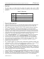
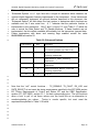
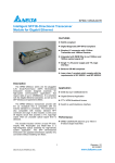
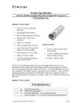
AN-2030: Digital Diagnostic Monitoring Interface for Optical Transceivers
Finisar
1
Application Note AN-2030
2
Digital Diagnostic Monitoring Interface
for SFP Optical Transceivers
3
4
5
6
7
1.
Scope and Overview
8
9
10
11
12
13
14
15
16
17
18
19
20
21
22
23
24
25
26
27
28
29
30
31
32
33
34
This document defines an enhanced digital diagnostic monitoring interface available in
Finisar SFP and GBIC optical transceivers. The i nterface allows real time access to
device operating parameters, and it includes a sophisticated system of alarm and
warning flags which alerts end-users when particular operating parameters are outside
of a factory set normal range. The interface is fully compliant with SFF-8472, “Digital
Diagnostic Monitoring Interface for Optical Transceivers", revision 9.3.
35
2.
These digital diagnostic features are implemented in all Finisar SFP transceivers that
contain a “D” in the part number suffix (for example, FTRJ -1319-7D-2.5), as well as
DWDM and CWDM GBICs. All next generation Finisar SFPs utilizing the new part
numbering scheme (e.g. FTRJ1621P1BCL) also have the same diagnostic capability.
The interface is an extension of the serial ID interface defined in the GBIC specification
as well as the SFP MSA. Both specifications define a 256-byte memory map in
EEPROM, which is accessible over a 2-wire serial interface at the 8 bit address
1010000X (A0h). The digital diagnostic monitoring interface makes use of the 8 bit
address 1010001X (A2h), so the originally defined serial ID memory map remains
unchanged. The interface is identical to, and is thus fully backward compatible with both
the GBIC Specification and the SFP Multi Source Agreement. The complete interface is
described in Section 3 below.
The operating and diagnostics information is monitored and reported by a Digital
Diagnostics Transceiver Controller (DDTC), which is accessed via a 2-wire serial bus.
Its physical characteristics are defined in Section 4.
Applicable Documents
36
37
38
39
40
41
42
43
44
45
46
47
Gigabit Interface Converter (GBIC). SFF document number: SFF-0053, rev. 5.5,
September 27, 2000.
Small Form Factor Pluggable (SFP) Transceiver MultiSource Agreement (MSA),
September 14, 2000.
Digital Diagnostic Monitoring Interface for Optical Transceivers: SFF-8472, Draft
Revision 9.3, August 1, 2002.
9/26/02 Revision D
Page 1
AN-2030: Digital Diagnostic Monitoring Interface for Optical Transceivers
Finisar
1
2
3
4
5
6
7
8
9
10
11
12
13
14
15
16
17
18
19
20
3.
Enhanced Digital Diagnostic Interface Definition
Overview
The enhanced digital diagnostic interface is a superset of the MOD-DEF interface
defined in the SFP MSA document dated September 14, 2000. The 2-wire interface pin
definitions, hardware, and timing are clearly defined there, as well as in Section 4
below. This section describes an extension to the memory map defined in the SFP
MSA. The enhanced interface uses the two wire serial bus address 1010001X (A2h) to
provide diagnostic information about the module’s present operating conditions. A
memory map is shown in Figure 3.1 below.
The transceiver generates this diagnostic data by digitization of internal analog signals.
Calibration and alarm threshold data is written during device manufacture.
In addition to generating digital readings of internal analog values, the device generates
various status bits based on comparison between current values and factory-preset
limits.
9/26/02 Revision D
Page 2
AN-2030: Digital Diagnostic Monitoring Interface for Optical Transceivers
1
2
3
4
5
6
Figure 3.1: Digital Diagnostic Memory Map
2 wire address 1010000X (A0h)
0
7
Serial ID Defined by
SFP MSA (96 bytes)
8
9
2 wire address 1010001X (A2h)
0
Alarm and Warning
Thresholds (56 bytes)
55
Cal Constants
(40 bytes)
10
11
95
12
14
16
95
Vendor Specific
(32 bytes)
13
15
Finisar
127
Real Time Diagnostic
Interface (24 bytes)
119
Password Entry (8 bytes)
127
17
18
19
Reserved in SFP
MSA (128 bytes)
20
21
User Writable
EEPROM (120 bytes)
22
23
24
247
25
26
255
255
Control Functions (8 bytes)
27
28
29
30
31
32
33
34
35
36
37
38
Specific Data Field Descriptions
39
40
41
The information in italics in Table 3.1 indicates fields that are specific to the digital
diagnostics functions.
42
9/26/02 Revision D
Page 3
AN-2030: Digital Diagnostic Monitoring Interface for Optical Transceivers
Finisar
Table 3.1 Serial ID: Data Fields – Address A0
1
Size
Data
(Bytes)
Address
0
1
1
1
Name of
Field
Identifier
Ext. Identifier
Description of Field
BASE ID FIELDS
Type of serial transceiver (see table 3.2)
Extended identifier of type of serial transceiver
2
1
Connector
3-10
8
Transceiver
11
1
Encoding
12
13
1
1
BR, Nominal
Reserved
14
1
Link length supported for 9/125 µm fiber, units of km
15
1
Length(9µm ) km
Length (9µm )
16
1
Length (50µm)
Link length supported for 50/125 µm fiber, units of 10 m
17
18
1
1
19
1
Reserved
20-35
36
16
1
Vendor name
Reserved
37-39
3
Vendor OUI
SFP vendor IEEE company ID
40-55
56-59
16
4
Vendor PN
Vendor rev
Part number provided by SFP vendor (ASCII)
Revision level for part number provided by vendor (ASCII)
60-61
2
Wavelength
Laser wavelength
62
63
1
1
Reserved
CC_BASE
64-65
2
Options
66
67
1
1
BR, max
BR, min
68-83
16
Vendor SN
84-91
92
8
1
93
1
94
1
95
1
Date code
Diagnostic
Monitoring Type
Enhanced
Options
SFF-8472
Compliance
CC_EXT
96-127
128-255
32
128
9/26/02 Revision D
Code for connector type (see table 3.3)
Code for electronic compatibility or optical compatibility
(see table 3.4)
Code for serial encoding algorithm (see table 3.5)
Nominal bit rate, units of 100 MBits/sec.
Link length supported for 9/125 µm fiber, units of 100 m
Length (62.5µm) Link length supported for 62.5/125 µm fiber, units of 10 m
Length (Copper) Link length supported for copper, units of meters
SFP vendor name (ASCII)
DWDM channel spacing - DWDM modules only
DWDM wavelength fraction - DWDM modules only
Check code for Base ID Fields (addresses 0 to 62)
EXTENDED ID FIELDS
Indicates which optional transceiver signals are implemented
(see table 3.6)
Upper bit rate margin, units of %
Lower bit rate margin, units of %
Serial number provided by vendor (ASCII)
Vendor’s manufacturing date code (see table 3.7)
Indicates which type of diagnostic monitoring is implemented (if
any) in the transceiver (see Table 3.8)
Indicates which optional enhanced features are implemented (if any)
in the transceiver (see Table 3.9)
Indicates which revision of SFF-8472 the transceiver complies with.
(see table 3.11)
Check code for the Extended ID Fields (addresses 64 to 94)
VENDOR SPECIFIC ID FIELDS
Vendor Specific Vendor Specific EEPROM
Reserved
Reserved for future use.
Page 4
AN-2030: Digital Diagnostic Monitoring Interface for Optical Transceivers
Finisar
1
Identifier
2
The identifier value specifies the physical device described by the serial information.
This value shall be included in the serial data. The defined identifier values are shown in
table 3.2. Finisar SFP modules have this byte set to 03h. Finisar GBIC modules have
this byte set to 01h.
3
4
5
TABLE 3.2: Identifier values
6
7
Value
Description of physical device
00h
01h
Unknown or unspecified
GBIC
02h
Module/connector soldered to motherboard
03h
04-7Fh
SFP
Reserved
80-FFh
Vendor specific
8
9
10
Extended Identifier
11
The extended identifier value provides additional information about the transceiver.
12
The field is set to 04h for all non-custom SFP and GBIC modules indicating serial ID
module definition.
13
14
15
Connector
16
17
18
19
20
The connector value indicates the external connector provided on the interface. This
value shall be included in the serial data. The defined connector values are shown in
table 3.3. Note that 01h – 05h are not SFP compatible, and are included for
compatibility with GBIC standards. Finisar optical SFP modules currently have this byte
set to 07h (optical LC connector). GBIC modules have the byte set to 01h (SC).
21
22
9/26/02 Revision D
Page 5
AN-2030: Digital Diagnostic Monitoring Interface for Optical Transceivers
Finisar
1
TABLE 3.3: Connector values
2
Value
Description of connector
00h
01h
Unknown or unspecified
SC
02h
Fibre Channel Style 1 copper connector
03h
04h
Fibre Channel Style 2 copper connector
BNC/TNC
05h
Fibre Channel coaxial headers
06h
07h
FiberJack
LC
08h
MT-RJ
09h
0Ah
MU
SG
0Bh
Optical pigtail
0C-1Fh Reserved
20h
HSSDC II
21h
Copper Pigtail
22h-7Fh Reserved
80-FFh Vendor specific
3
4
9/26/02 Revision D
Page 6
AN-2030: Digital Diagnostic Monitoring Interface for Optical Transceivers
Finisar
1
Transceiver
2
The following bit significant indicators define the electronic or optical interfaces that are
supported by the transceiver. At least one bit shall be set in this field. For Fibre Channel
transceivers, the Fibre Channel speed, transmission media, transmitter technology, and
distance capability shall all be indicated. The SONET Compliance Codes are described
in more detail in table 3.4a.
3
4
5
6
Table 3.4: Transceiver codes
7
8
Data Bit
Addr
1
Description of transceiver
1
Data Bit
Addr
Reserved Standard Compliance Codes
3
7-0
Reserved
4
7-5
Reserved
SONET Compliance Codes
Description of transceiver
Fibre Channel link length
7
7
very long distance (V)
7
7
6
5
short distance (S)
intermediate distance (I)
4
long distance (L)
4
4
SONET reach specifier bit 1
7
4
4
3
2
SONET reach specifier bit 2
OC 48, long reach
Fibre Channel transmitter technology
7
3-2
Reserved
4
1
OC 48, intermediate reach
7
1
Longwave laser (LC)
4
5
0
7
OC 48 short reach
Reserved
7
8
0
7
Electrical inter-enclosure (EL)
Electrical intra-enclosure (EL)
5
6
OC 12, single mode long reach
8
6
Shortwave laser w/o OFC (SN)
5
5
5
4
OC 12, single mode inter. reach
OC 12 multi-mode short reach
8
8
5
4
Shortwave laser w/ OFC (SL)
Longwave laser (LL)
5
3
Reserved
8
0-3
Reserved
5
5
2
1
OC 3, single mode long reach
OC 3, single mode inter. reach
5
0
OC 3, multi-mode short reach
Gigabit Ethernet Compliance Codes
Fibre Channel transmission media
9
7
Twin Axial Pair (TW)
9
9
6
5
Shielded Twisted Pair (TP)
Miniature Coax (MI)
9
4
Video Coax (TV)
6
6
7-4
3
Reserved
1000BASE-T
9
9
3
2
Multi-mode, 62.5m (M6)
Multi-mode, 50 m (M5)
6
2
1000BASE-CX
9
1
Reserved
6
6
1
0
1000BASE-LX
1000BASE-S X
9
0
Single Mode (SM)
Fibre Channel speed
10
10
7-5
4
Reserved
400 MBytes/Sec
10
3
Reserved
10
10
2
1
200 MBytes./Sec
Reserved
10
0
100 MBytes/Sec
1
Bit 7 is the high order bit and is transmitted first in each byte.
9/26/02 Revision D
Page 7
Finisar
AN-2030: Digital Diagnostic Monitoring Interface for Optical Transceivers
9
10
The SONET compliance code bits allow the host to determine with which specifications
a SONET transceiver complies. For each bit rate defined in Table 3.5 (OC-3, OC-12,
OC-48), SONET specifies short reach (SR), intermediate reach (IR), and long reach
(LR) requirements. For each of the three bit rates, a single short reach (SR)
specification is defined. Two variations of intermediate reach (IR-1, IR-2) and three
variations of long reach (LR-1, LR-2, and LR-3) are also defined for each bit rate. Byte
4, bits 0-2, and byte 5, bits 0-7 allow the user to determine which of the three reaches
has been implemented – short, intermediate, or long. Two additional bits (byte 4, bits 34) are necessary to discriminate between different intermediate or long reach variations.
These codes are defined in Table 3.4a.
11
Table 3.4a: SONET Reach Specifiers
1
2
3
4
5
6
7
8
Speed
Reach
Specifier bit 1
Specifier bit 2
Description
OC-3/OC-12/OC-48
Short
0
0
SONET SR compliant
OC-3/OC-12/OC-48
Intermediate
1
0
SONET IR-1 compliant
OC-3/OC-12/OC-48
Intermediate
0
1
SONET IR-2 compliant
OC-3/OC-12/OC-48
Long
1
0
SONET LR-1 compliant
OC-3/OC-12/OC-48
Long
0
1
SONET LR-2 compliant
OC-3/OC-12/OC-48
Long
1
1
SONET LR-3 compliant
12
13
Encoding
14
16
17
18
The encoding value indicates the serial encoding mechanism that is the nominal design
target of the particular SFP. The value shall be contained in the serial data. The defined
encoding values are shown in table 3.5. Finisar Gigabit Ethernet/Fibre Channel
transceivers have this byte set to 01h (8B/10B encoding), and SONET transceivers
(including all SONET multi-rate transceivers) are set to 05h (SONET Scrambled).
19
Table 3.5: Encoding codes
15
20
Code
Description of encoding mechanism
00h
Unspecified
01h
02h
8B10B
4B5B
03h
NRZ
04h
05h
Manchester
SONET Scrambled
06h -FFh Reserved
21
22
9/26/02 Revision D
Page 8
AN-2030: Digital Diagnostic Monitoring Interface for Optical Transceivers
Finisar
1
BR, nominal
2
The nominal bit rate (BR, nominal) is specified in units of 100 Megabits per second,
rounded off to the nearest 100 Megabits per second. The bit rate includes those bits
necessary to encode and delimit the signal as well as those bits carrying data
information. A value of 0 indicates that the bit rate is not specified and must be
determined from the transceiver technology. The actual information transfer rate will
depend on the encoding of the data, as defined by the encoding value.
3
4
5
6
7
8
9
10
11
12
13
14
15
16
Length (9µ)-km
Note that this field is an addition to EEPROM data from the original GBIC definition.
This value specifies the link length that is supported by the transceiver while operating
in compliance with the applicable standards using single mode fiber. The value is in
units of kilometers. A value of 255 means that the transceiver supports a link length
greater than 254 km. A value of zero means that the transceiver does not support single
mode fiber or that the length information must be determined from the transceiver
technology.
17
18
Length (9µ)
19
This value specifies the link length that is supported by the transceiver while operating
in compliance with the applicable standards using single mode fiber. The value is in
units of 100 meters. A value of 255 means that the transceiver supports a link length
greater than 25.4 km. A value of zero means that the transceiver does not support
single mode fiber or that the length information must be determined from the transceiver
technology.
20
21
22
23
24
25
26
Length (50µ)
27
This value specifies the link length that is supported by the transceiver while operating
in compliance with the applicable standards using 50 micron multi-mode fiber. The
value is in units of 10 meters. A value of 255 means that the transceiver supports a link
length greater than 2.54 km. A value of zero means that the transceiver does not
support 50 micron multi-mode fiber or that the length information must be determined
from the transceiver technology.
28
29
30
31
32
33
34
Length (62.5µ)
35
This value specifies the link length that is supported by the transceiver while operating
in compliance with the applicable standards using 62.5 micron multi-mode fiber. The
value is in units of 10 meters. A value of 255 means that the transceiver supports a link
length greater than 2.54 km. A value of zero means that the transceiver does not 62.5
micron multi-mode fiber or that the length information must determined from the
36
37
38
39
9/26/02 Revision D
Page 9
AN-2030: Digital Diagnostic Monitoring Interface for Optical Transceivers
1
2
Finisar
transceiver technology. It is common for the transceiver to support both 50 micron and
62.5 micron fiber.
3
4
Length (Copper)
5
This value specifies the minimum link length that is supported by the transceiver while
operating in compliance with the applicable standards using copper cable. The value is
in units of 1 meter. A value of 255 means that the transceiver supports a link length
greater than 254 meters. A value of zero means that the transceiver does not support
copper cables or that the length information must be determined from the transceiver
technology. Further information about the cable design, equalization, and connectors is
usually required to guarantee meeting a particular length requirement.
6
7
8
9
10
11
12
13
Vendor name
14
The vendor name is a 16 character field that contains ASCII characters, left-aligned and
padded on the right with ASCII spaces (20h). The vendor name shall be the full name of
the corporation, a commonly accepted abbreviation of the name of the corporation, the
SCSI company code for the corporation, or the stock exchange code for the corporation.
At least one of the vendor name or the vendor OUI fields shall contain valid serial data.
Finisar transceivers contain the text string “FINISAR CORP.” in this address.
15
16
17
18
19
20
21
DWDM Channel Spacing
22
Byte 36 is reserved (set to 00h) in the SFP MSA as well as in SFF-8472. Finisar
DWDM transceivers use this byte to indicate their channel spacing. DWDM channel
spacing is an 8 bit unsigned integer indicating the DWDM channel spacing in units of
gigahertz. This byte is set to 00h in all non-DWDM Finisar transceivers.
23
24
25
26
27
Vendor OUI
28
The vendor organizationally unique identifier field (vendor OUI) is a 3-byte field that
contains the IEEE Company Identifier for the vendor. A value of all zero in the 3-byte
field indicates that the Vendor OUI is unspecified. Finisar transceivers contain the
values 00h, 90h and 65h in these addresses.
29
30
31
32
33
Vendor PN
34
The vendor part number (vendor PN) is a 16-byte field that contains ASCII characters,
left-aligned and padded on the right with ASCII spaces (20h), defining the vendor part
number or product name. A value of all zero in the 16-byte field indicates that the
vendor PN is unspecified.
35
36
37
38
9/26/02 Revision D
Page 10
AN-2030: Digital Diagnostic Monitoring Interface for Optical Transceivers
Finisar
1
Vendor Rev
2
The vendor revision number (vendor rev) is a 4-byte field that contains ASCII
characters, left-aligned and padded on the right with ASCII spaces (20h), defining the
vendor’s product revision number. A value of all zero in the 4-byte field indicates that
the vendor rev is unspecified. All legacy Finisar transceivers contain zero in all 4 bytes
or ASCII space (20h) in all four bytes or one of two place holders: “X1—“ or “1A—“.
Early versions of the digital diagnostic standard (SFF-8472), used a scale factor of
1µA/AD Count for interpreting laser bias current readings. SFF-8472 later changed the
scale factor to 2µA/AD Count. All Finisar modules using a scale factor of 2µA/AD Count
have an ASCII “A” written in byte 56 of this field.
3
4
5
6
7
8
9
10
11
12
Laser Wavelength
13
Nominal transmitter output wavelength at room temperature. This field is a 16 bit value
with byte 60 as high order byte and byte 61 as low order byte. The laser wavelength is
equal to the the 16 bit integer value in nm. This field allows the user to read the laser
wavelength directly, so it is not necessary to infer it from the transceiver “Code for
Electronic Compatibility” (bytes 3 – 10). This also allows specification of wavelengths
not covered in bytes 3 – 10, such as those used in coarse WDM systems.
14
15
16
17
18
19
20
DWDM Wavelength Fraction
21
24
25
Byte 62 is reserved (set to 00h) in the SFP MSA as well as SFF-8472. Finisar DWDM
transceivers use this byte in conjunction with bytes 60-61 to indicate the DWDM
transceiver laser wavelength. Bytes 60-61 provide the integer wavelength in units of
nm. In DWDM transceivers, by 62 provides the fractional wavelength in units of
0.01nm. Thus the wavelength for a particular DWDM transceiver is given by:
26
27
(byte 60,61) + (byte 62 * 0.01nm). In all non-DWDM Finisar transceivers, this byte is set
to 00h.
22
23
28
29
CC_BASE
30
The check code is a one byte code that can be used to verify that the first 64 bytes of
serial information in the SFP is valid. The check code shall be the low order 8 bits of the
sum of the contents of all the bytes from byte 0 to byte 62, inclusive.
31
32
33
34
9/26/02 Revision D
Page 11
AN-2030: Digital Diagnostic Monitoring Interface for Optical Transceivers
Finisar
1
Options
2
The bits in the option field shall specify the options implemented in the transceiver as
described in table 3.6. StandardFinisar SFP transceivers do not implement TX_FAULT
or RATE_SELECT, so byte 65 set to 00010010b.
3
4
5
Table 3.6: Option values
6
Data
Bit
Description of option
Address
64
7-0 Reserved
65
7-6 Reserved
65
5
Indicates if RATE_SELECT is implemented. Finisar does not
implement this feature.
NOTE: Lack of implemention does not indicate lack of
simultaneous compliance with multiple standard rates.
Compliance with particular standards should be determined
from Transceiver Code Section (Table 3.4)
65
65
4
3
TX_DISABLE is implemented and disables the serial output.
TX_FAULT signal implemented.
65
2
Loss of Signal implemented, signal inverted from definition in
Table 1 of the SFP MSA.
NOTE: This is not standard SFP/GBIC behavior and should
be avoided, since non-interoperable behavior results.
65
1
Loss of Signal implemented, signal as defined in Table 1 of
the SFP MSA.
65
0
Reserved
7
8
BR, max
9
The upper bit rate limit at which the transceiver will still meet its specifications (BR, max)
is specified in units of 1% above the nominal bit rate. A value of zero indicates that this
field is not specified.
10
11
12
13
BR, min
14
The lower bit rate limit at which the transceiver will still meet its specifications (BR, min)
is specified in units of 1% below the nominal bit rate. A value of zero indicates that this
field is not specified.
15
16
17
18
Vendor SN
19
The vendor serial number (vendor SN) is a 16 character field that contains ASCII
characters, left-aligned and padded on the right with ASCII spaces (20h), defining the
vendor’s serial number for the transceiver. A value of all zero in the 16-byte field
indicates that the vendor PN is unspecified.
20
21
22
9/26/02 Revision D
Page 12
AN-2030: Digital Diagnostic Monitoring Interface for Optical Transceivers
Finisar
1
2
Date Code
3
4
5
The date code is an 8-byte field that contains the vendor’s date code in ASCII
characters. The date code is mandatory. The date code shall be in the format specified
by table 3.7.
6
Table 3.7: Date Code
7
Data
Description of field
Address
84-85
86-87
ASCII code, two low order digits of year. (00 = 2000).
88-89
ASCII code, digits of month (01 = Jan through 12 =
Dec)
ASCII code, day of month (01 - 31)
90-91
ASCII code, vendor specific lot code, may be blank
8
9
Diagnostic Monitoring Type
10
11
“Diagnostic Monitoring Type” is a 1 byte field with 8 single bit indicators describing how
diagnostic monitoring is implemented in the particular transceiver (see Table 3.8).
12
Bit 6, address 92, is set in Finisar ‘7D’ SFPs, 'P' SFPs under the new part numbering
scheme, and WDM GBICs, indicating that digital diagnostic monitoring has been
implemented. Received power monitoring, transmitted power monitoring, bias current
monitoring, supply voltage monitoring and temperature monitoring are all implemented.
Additionally, alarm and warning thresholds are written as specified in this document at
locations 00 – 55 on 2 wire serial address 1010001X (A2h) (see Table 3.14).
13
14
15
16
17
18
19
20
21
22
23
24
25
26
27
28
29
30
31
32
33
34
If bit 5, “internally calibrated”, is set, the transceiver reports calibrated values directly
in units of current, power etc. If bit 4, “externally calibrated”, is set, the reported
values are A/D counts which must be converted to real world units using calibration
values read using 2 wire serial address 1010001X (A2h) from bytes 55 - 95. Finisar
transceivers use both calibration types so it is necessary to read bit 5 in order to
properly interpret transceiver data .
Bit 3 indicates whether the received power measurement represents average input
optical power or OMA. If the bit is set, average power is monitored. If it is not, OMA is
monitored. Finisar transceivers report “average power” and thus bit 3 is set.
Bit 2 indicates whether or not a special “address change” sequence (described in SFF8472) is required. This sequence is NOT required in Finisar modules. Information at
both 2-wire addresses (A0h and A2h) may be accessed simply by using the appropriate
address during the 2-wire communication sequence.
Finisar SFP/GBIC transceivers thus have 0b01111000 written at address 92 if they are
internally calibrated, and 0b01011000 written at address 92 if they are externally
calibrated. Note that internally calibrated devices can be treated as externally calibrated
devices because the external calibration constants are set to 1 or 0 as appropriate.
9/26/02 Revision D
Page 13
Finisar
AN-2030: Digital Diagnostic Monitoring Interface for Optical Transceivers
Table 3.8: Diagnostic Monitoring Type
1
Data Address
Bits
92
7
Description
Reserved
for
legacy
diagnostic
implementations. Must be ‘0’ for compilance
with this document.
92
6
Digital
diagnostic
monitoring
implemented
(described in this document). Must be ‘1’ for
compliance with this document.
92
5
Internally Calibrated
92
4
Externally Calibrated
92
3
Received power measurement type
0 = OMA, 1 = Average Power
92
2
Address change required see section above,
“addressing modes”
92
1-0
Reserved
2
3
9/26/02 Revision D
Page 14
AN-2030: Digital Diagnostic Monitoring Interface for Optical Transceivers
Finisar
1
Enhanced Options
2
10
11
“Enhanced Options” is a 1 byte field with 8 single bit indicators which describe the
optional digital diagnostic features implemented in the transceiver. Since transceivers
will not necessarily implement all optional features described in this document, the
“Enhanced Options” bit field allows the host system to determine which functions are
available over the 2 wire serial bus. A ‘1’ indicates that the particular function is
implemented in the transceiver. Bits 3 and 6 of byte 110 (see Table 3.17) allow the
user to control the Rate_Select and TX_Disable functions. If these functions are not
implemented, the bits remain readable and writable, but the transceiver ignores them.
Finisar transceivers with alarm and warning flags enabled contain the value
0b10010000 at location 93.
12
Table 3.9: Enhanced Options
3
4
5
6
7
8
9
Data Address
Bits
Description
93
7
Optional Alarm/warning flags implemented for
all monitored quantities (see Table 3.18)
93
6
Optional Soft TX_DISABLE control and
monitoring implemented
93
5
Optional Soft TX_FAULT monitoring
implemented
93
4
Optional Soft RX_LOS monitoring
implemented
93
3
Optional Soft RATE_SELECT control and
monitoring implemented
93
2-0
Reserved
13
14
15
16
17
18
19
20
21
22
Note that the “soft” control functions - TX_DISABLE, TX_FAULT, RX_LOS, and
RATE_SELECT do not meet the timing requirements specified in the SFP MSA section
B3 “Timing Requirements of Control and Status I/O” and the GBIC Specification,
revision 5.5, (SFF-8053), section 5.3.1, for their corresponding pins. The soft functions
allow a host to poll or set these values over the serial bus as an alternative to
monitoring/setting pin values.
Timing is vendor specific, but must meet the
requirements specified in Table 3.10 below.
23
24
25
26
27
9/26/02 Revision D
Page 15
AN-2030: Digital Diagnostic Monitoring Interface for Optical Transceivers
Finisar
1
Table 3.10: I/O Timing for Soft Control & Status Functions
2
Parameter
Symbol
TX_DISABLE assert time
Max
Units
Conditions
t_off
100
ms
TX_DISABLE deassert time
t_on
100
ms
Time to initialize, including
reset of TX_FAULT
t_init
300
ms
TX_FAULT assert time
t_fault
100
ms
LOS assert time
t_loss_on
100
ms
LOS deassert time
t_loss_off
100
ms
Rate select change time
T_rate_sel
100
ms
Serial ID clock rate
f_serial_cl
ock
t_data
100
kHz
Time from TX_DISABLE bit set
until optical output falls below
10% of nominal
Time from TX_DISABLE bit
1
cleared until optical output rises
above 90% of nominal
From power on or negation of
TX_FAULT using TX_DISABLE;
serial communication possible
Time from fault to TX_FAULT bit
set.
Time from LOS state to RX_LOS
bit set
Time from non-LOS state to
RX_LOS bit cleared
Time from change of state of Rate
1
Select bit until receiver
bandwidth is in conformance with
appropriate specification
n/a
1000
ms
Analog parameter data ready
1
Min
1
From power on to data ready, bit
0 of byte 110 set
measured from falling clock edge after stop bit of write transaction.
3
4
SFF-8472 Compliance
5
6
Byte 94 contains an unsigned integer that indicates which feature set(s) are
implemented in the transceiver.
7
Table 3.11: SFF-8472 Compliance
8
Data Address
Value
Interpretation
94
0
Digital diagnostic functionality not included or
undefined.
94
1
Includes functionality described in Rev 9.3
SFF-8472.
94
2
TBD
94
3
TBD
9
10
CC_EXT
11
The check code is a one byte code that can be used to verify that the first 32 bytes of
extended serial information in the SFP is valid. The check code shall be the low order 8
bits of the sum of the contents of all the bytes from byte 64 to byte 94, inclusive.
12
13
9/26/02 Revision D
Page 16
AN-2030: Digital Diagnostic Monitoring Interface for Optical Transceivers
Finisar
1
2
Diagnostics
3
4
5
2 wire serial bus address 1010001X (A2h) is used to access measurements of
transceiver temperature, internally measured supply voltage, TX bias current, TX output
power, received optical power, and two additional quantities to be defined in the future.
6
7
8
9
10
The values are interpreted differently depending upon the option bits set at address 92.
If bit 5 “internally calibrated” is set, the values are calibrated absolute measurements,
which should be interpreted according to the section “Internal Calibration” below. If bit 4
“externally calibrated” is set, the values are A/D counts, which are converted into real
units per the subsequent section titled “External Calibration”.
11
12
13
14
15
Measured parameters are reported in 16 bit data fields, i.e., two concatenated bytes.
To guarantee coherency of the diagnostic monitoring data, the host is required to
retrieve any multi-byte fields from the diagnostic monitoring data structure (IE: Rx Power
MSB - byte 104 in A2h, Rx Power LSB - byte 105 in A2h) by the use of a single twobyte read sequence across the serial interface.
16
17
18
Measurements are calibrated over specified device operating temperature and voltage
and should be interpreted as defined below. Alarm and warning threshold values
should be interpreted in the same manner as real time 16 bit data.
19
Internal Calibration
20
21
22
23
24
25
1) Internally measured transceiver temperature. Represented as a 16 bit signed twos
complement value in increments of 1/256 degrees Celsius, yielding a total range of –
128°C to +128°C. Temperature measurement is valid from –40°C to +125°C with an
accuracy of ± 3°C. The temperature sensor is located in the center of the module
and is typically 5 to 10 degrees ho tter than the module case. See Tables 3.12 and
3.13 below for examples of temperature format.
26
27
28
2) Internally measured transceiver supply voltage. Represented as a 16 bit unsigned
integer with the voltage defined as the full 16 bit value (0 – 65535) with LSB equal to
100 µVolt, yielding a total range of 0 to +6.55 Volts. Accuracy is ±100mV.
29
30
31
32
33
34
35
36
37
3) Measured TX bias current in µA. Represented as a 16 bit unsigned integer with the
current defined as the full 16 bit value (0 – 65535) with LSB equal to 2 µA, yielding a
total range of 0 to 131 mA. Accuracy is ± 10%. Early versions of the digital
diagnostic standard (SFF-8472) used a scale factor of 1µA/AD Count for interpreting
laser bias current readings. SFF-8472 later changed the scale factor to the current
value of 2µA/AD Count. All Finisar modules using a scale factor of 2µA/AD Count
have an ASCII “A” written in byte 56 of the ‘vendor rev’ field (see table 3.1). Legacy
Finisar modules using a scale factor of 1µA/AD Count contain either zero or ASCII
space (20h) or one of two place holders: “X1—“, “1A—“, in location 56.
38
39
40
4) Measured TX output power in mW. Represented as a 16 bit unsigned integer with
the power defined as the full 16 bit value (0 – 65535) with LSB equal to 0.1 µW,
yielding a total range of 0 to 6.5535 mW (~ -40 to +8.2 dBm). Data is factory
9/26/02 Revision D
Page 17
Finisar
AN-2030: Digital Diagnostic Monitoring Interface for Optical Transceivers
1
2
calibrated to absolute units using the most representative fiber output type.
Accuracy is ±3dB. Data is not valid when the transmitter is disabled.
3
4
5
6
7
8
5) Measured RX received average optical power in mW. Represented as a 16 bit
unsigned integer with the power defined as the full 16 bit value (0 – 65535) with LSB
equal to 0.1 µW, yielding a total range of 0 to 6.5535 mW (~ -40 to +8.2 dBm).
Absolute accuracy is dependent upon the exact optical wavelength. For the
specified wavelength, accuracy is ±3dB. See module specification sheet for range
over which accuracy requirement is met.
9
10
11
Tables 3.12 and 3.13 below illustrate the 16 bit signed twos complement format used for
temperature reporting. The most significant bit (D7) represents the sign, which is zero
for positive temperatures and one for negative temperatures.
Table 3.12: Bit weights (°C) for temperature reporting registers
12
13
14
D7
SIGN
Most Significant Byte (byte 96)
D6 D5 D4 D3 D2 D1
64
32
16
8
4
2
D0
D7
1
1/2
Least Significant Byte (byte 97)
D6 D5 D4 D3 D2 D1
1/4
1/8
1/16
1/32
1/64
1/128
D0
1/256
15
Table 3.13: Digital temperature format
16
17
18
19
20
21
22
23
24
Temperature
BINARY
HEXADECIMAL
DECIMAL
FRACTION
HIGH BYTE
LOW BYTE
HIGH BYTE
LOW BYTE
+127.996
+125.000
+25.000
+1.004
+1.000
+0.996
+0.004
0.000
-0.004
-1.000
-25.000
-40.000
-127.996
-128.000
+127 255/256
+125
+25
+1 1/256
+1
+255/256
+1/256
0
-1/256
-1
-25
-40
-127 255/256
-128
01111111
01111101
00011001
00000001
00000001
00000000
00000000
00000000
11111111
11111111
11100111
11011000
10000000
10000000
11111111
00000000
00000000
00000001
00000000
11111111
00000001
00000000
11111111
00000000
00000000
00000000
00000001
00000000
7F
7D
19
01
01
00
00
00
FF
FF
E7
D8
80
80
FF
00
00
01
00
FF
01
00
FF
00
00
00
01
00
25
26
27
28
9/26/02 Revision D
Page 18
AN-2030: Digital Diagnostic Monitoring Interface for Optical Transceivers
Finisar
1
External Calibration
2
3
4
5
6
Measurements are raw A/D values and must be converted to real units using calibration
constants stored in EEPROM locations 56 – 95 at 2 wire serial bus address A2h (see
Table 3.15). Calibration is valid over specified device operating temperature and
voltage. Alarm and warning threshold values should be interpreted in the same manner
as real time 16 bit data.
7
8
9
10
11
12
13
1) Internally measured transceiver temperature. Module temperature, T, is given by the
following equation: T(C) = Tslope * TAD (16 bit signed twos complement value) + Toffset.
The result is in units of 1/256C, yielding a total range of –128C to +128C. See Table
3.15 for locations of TSLOPE and TOFFSET. Temperature measurement is valid from –
40°C to +125°C with an accuracy of ± 3°C. The temperature sensor is located in the
center of the module and is typically 5 to 10 degrees hotter than the module case. See
Tables 3.12 and 3.13 above for examples of temperature format.
14
15
16
17
2) Internally measured transceiver supply voltage. Module internal supply voltage, V, is
given in microvolts by the following equation: V(µV) = VSLOPE * VAD (16 bit unsigned
integer) + VOFFSET . The result is in units of 100µV, yielding a total range of 0 – 6.55V.
See Table 3.15 for locations of V SLOPE and V OFFSET . Accuracy is ±100mV.
18
19
20
21
22
23
24
25
26
27
3) Measured transmitter laser bias current. Module laser bias current, I, is given by the
following equation: I(µA) = ISLOPE * IAD (16 bit unsigned integer) + IOFFSET . This result is
in units of 2 µA, yielding a total range of 0 to 131 mA. See Table 3.15 for locations of
ISLOPE and IOFFSET. Accuracy is ± 10%. Early versions of the digital diagnostic standard
(SFF-8472) used a scale factor of 1µA/AD Count for interpreting laser bias current
readings. SFF-8472 later changed the scale factor to the current value of 2µA/AD
Count. All Finisar modules using a scale factor of 2µA/AD Count have an ASCII “A”
written in byte 56 of the ‘vendor rev’ field (see table 3.1). Legacy Finisar modules using
a scale factor of 1µA/AD Count contain either zero or ASCII space (20h) or one of two
place holders: “X1—“, “1A—“, in location 56.
28
29
30
31
32
33
34
4) Measured coupled TX output power. Module transmitter coupled output power,
TX_PWR, is given in µW by the following equation: TX_PWR (µW) = TX_PWRSLOPE *
TX_PWRAD (16 bit unsigned integer) + TX_PWROFFSET. This result is in units of 0.1µW
yielding a total range of 0 – 6.5mW. See Table 3.15 for locations of TX_PWRSLOPE and
TX_PWROFFSET.
Data is factory calibrated to absolute units using the most
representative fiber output type. Accuracy is ±3dB. Data is not valid when the
transmitter is disabled.
35
9/26/02 Revision D
Page 19
Finisar
AN-2030: Digital Diagnostic Monitoring Interface for Optical Transceivers
1
2
5) Measured received optical power. Received power, RX_PWR, is given in µW by
the following equation:
3
4
5
Rx_PWR (µW) = Rx_PWR(4) * Rx_PWRAD4 (16 bit unsigned integer) +
Rx_PWR(3)*Rx_PWRAD3 (16 bit unsigned integer) + Rx_PWR(2)*Rx_PWRAD2 (16 bit
unsigned integer) + Rx_PWR(1) *Rx_PWRAD (16 bit unsigned integer) + Rx_PWR(0)
6
7
8
9
10
The result is in units of 0.1µW yielding a total range of 0 – 6.5mW. See Table 3.15 for
locations of Rx_PWR(4-0). Absolute accuracy is dependent upon the exact optical
wavelength. For the specified wavelength, accuracy shall be better than ±3dB over
specified temperature and voltage. See module specification sheet for range over
which accuracy requirement is met.
11
12
Alarm and Warning Thresholds
13
14
15
16
Each A/D quantity has a corresponding high alarm, low alarm, high warning and low
warning threshold. These factory preset values allow the user to determine when a
particular value is outside of “normal” limits. These values vary with different
technologies and implementations.
17
18
Table 3.14: Alarm and Warning Thresholds (2-Wire Address A2h)
Address
# Bytes
Name
Description
00-01
2
Temp High Alarm
02-03
2
Temp Low Alarm
MSB at low address
MSB at low address
04-05
2
Temp High Warning
MSB at low address
06-07
2
Temp Low Warning
MSB at low address
08-09
2
Voltage High Alarm
MSB at low address
10-11
2
Voltage Low Alarm
MSB at low address
12-13
2
Voltage High Warning
MSB at low address
14-15
2
Voltage Low Warning
MSB at low address
16-17
2
Bias High Alarm
MSB at low address
18-19
2
Bias Low Alarm
MSB at low address
20-21
2
Bias High Warning
MSB at low address
22-23
2
Bias Low Warning
MSB at low address
24-25
2
TX Power High Alarm
MSB at low address
26-27
2
TX Power Low Alarm
MSB at low address
28-29
2
TX Power High Warning
MSB at low address
30-31
2
TX Power Low Warning
MSB at low address
32-33
2
RX Power High Alarm
MSB at low address
34-35
2
RX Power Low Alarm
MSB at low address
36-37
2
RX Power High Warning
MSB at low address
38-39
2
RX Power Low Warning
MSB at low address
40-55
16
Reserved
Reserved for future monitored quantities
19
20
21
9/26/02 Revision D
Page 20
AN-2030: Digital Diagnostic Monitoring Interface for Optical Transceivers
1
2
3
4
5
Finisar
Calibration Constants
TABLE 3.15: Calibration constants for External Calibration Option
(2 Wire Address A2h)
Address
# Bytes
Name
Description
56-59
4
Rx_PWR(4)
Single precision floating point calibration data - Rx optical power. Bit
7 of byte 56 is MSB. Bit 0 of byte 59 is LSB. Rx_PWR(4) is set to
zero for “internally calibrated” devices.
60-63
4
Rx_PWR(3)
64-67
4
Rx_PWR(2)
68-71
4
Rx_PWR(1)
72-75
4
Rx_PWR(0)
Single precision floating point calibration data - Rx optical power.
Bit 7 of byte 60 is MSB. Bit 0 of byte 63 is LSB. Rx_PWR(3) is set to
zero for “internally calibrated” devices.
Single precision floating point calibration data, Rx optical power.
Bit 7 of byte 64 is MSB, bit 0 of byte 67 is LSB. Rx_PWR(2) is set to
zero for “internally calibrated” devices.
Single precision floating point calibration data, Rx optical power. Bit 7
of byte 68 is MSB, bit 0 of byte 71 is LSB. Rx_PWR(1) is set to 1 for
“internally calibrated” devices.
Single precision floating point calibration data, Rx optical power. Bit 7
of byte 72 is MSB, bit 0 of byte 75 is LSB. Rx_PWR(0) is set to zero
for “internally calibrated” devices.
76-77
2
Tx_I(Slope)
78-79
2
Tx_I(Offset)
80-81
2
Tx_PWR(Slope)
82-83
2
Tx_PWR(Offset)
84-85
2
T (Slope)
86-87
2
T (Offset)
88-89
2
V (Slope)
90-91
2
V (Offset)
92-4
3
Reserved
Fixed decimal (unsigned) calibration data, internal module supply
voltage. Bit 7 of byte 88 is MSB, bit 0 of byte 89 is LSB. V(Slope) is
set to 1 for “internally calibrated” devices.
Fixed decimal (signed two’s complement) calibration data, internal
module supply voltage. Bit 7 of byte 90 is MSB. Bit 0 of byte 91 is
LSB. V(Offset) is set to zero for “internally calibrated” devices.
Reserved
95
1
Checksum
Byte 95 contains the low order 8 bits of the sum of bytes 0 – 94.
Fixed decimal (unsigned) calibration data, laser bias current. Bit 7 of
byte 76 is MSB, bit 0 of byte 77 is LSB. Tx_I(Slope) is set to 1 for
“internally calibrated” devices.
Fixed decimal (signed two’s complement) calibration data, laser bias
current. Bit 7 of byte 78 is MSB, bit 0 of byte 79 is LSB. Tx_I(Offset)
is set to zero for “internally calibrated” devices.
Fixed decimal (unsigned) calibration data, transmitter coupled output
power. Bit 7 of byte 80 is MSB, bit 0 of byte 81 is LSB.
Tx_PWR(Slope) is set to 1 for “internally calibrated” devices.
Fixed decimal (signed two’s complement) calibration data,
transmitter coupled output power. Bit 7 of byte 82 is MSB, bit 0 of
byte 83 is LSB. Tx_PWR(Offset) is set to zero for “internally
calibrated” devices.
Fixed decimal (unsigned) calibration data, internal module
temperature. Bit 7 of byte 84 is MSB, bit 0 of byte 85 is LSB.
T(Slope) is set to 1 for “internally calibrated” devices.
Fixed decimal (signed two’s complement) calibration data, internal
module temperature. Bit 7 of byte 86 is MSB, bit 0 of byte 87 is LSB.
T(Offset) is set to zero for “internally calibrated” devices.
6
7
8
9/26/02 Revision D
Page 21
Finisar
AN-2030: Digital Diagnostic Monitoring Interface for Optical Transceivers
1
2
3
4
5
6
7
8
9
10
11
12
The slope constants at addresses 76, 80,84, and 88, are unsigned fixed-point binary
numbers. The slope will therefore always be positive. The binary point is in between
the upper and lower bytes, i.e., between the eight and ninth most significant bits. The
most significant byte is the integer portion in the range 0 to +255. The least significant
byte represents the fractional portion in the range of 0.00391 (1/256) to 0.9961
(255/256). The smallest real number that can be represented by this format is 0.00391
(1/256); the largest real number that can be represented using this format is 255.9961
(255 + 255/256). Slopes are defined, and conversion formulas found, in the “External
Calibration” section. Examples of this format are illustrated below:
Table 3.16a: Unsigned fixed-point binary format for slopes
Decimal
Value
0.0000
0.0039
1.0000
1.0313
1.9961
2.0000
255.9921
255.9961
13
14
15
16
17
18
19
20
21
22
23
24
25
26
27
28
29
30
Binary Value
MSB
LSB
00000000
00000000
00000001
00000001
00000001
00000010
11111111
11111111
00000000
00000001
00000000
00001000
11111111
00000000
11111110
11111111
Hexadecimal Value
High Byte
Low Byte
00
00
01
01
01
02
FF
FF
00
01
00
08
FF
00
FE
FF
The calibration offsets are 16-bit signed twos complement binary numbers. The offsets
are defined by the formulas in the “External Calibration” section. The least significant bit
represents the same units as described above under “Internal Calibration” for the
corresponding analog parameter, e.g., 2µA for bias current, 0.1µW for optical power,
etc. The range of possible integer values is from +32767 to -32768. Examples of this
format are shown below.
Table 3.16b: Format for offsets
Binary Value
Hexadecimal Value
Decimal
Value
High Byte
Low Byte
High Byte
Low Byte
+32767
+3
+2
+1
0
-1
-2
-3
-32768
01111111
00000000
00000000
00000000
00000000
11111111
11111111
11111111
10000000
1111111
00000011
00000010
00000001
00000000
11111111
11111110
11111101
00000000
7F
00
00
00
00
FF
FF
FF
80
FF
03
02
01
00
FF
FE
FD
00
External calibration of received optical power makes use of single-precision floatingpoint numbers as defined by IEEE Standard for Binary Floating-Point Arithmetic, IEEE
Std 754-1985. Briefly, this format utilizes four bytes (32 bits) to represent real
numbers. The first and most significant bit is the sign bit; the next eight bits indicate an
exponent in the range of +126 to –127; the remaining 23 bits represent the mantissa.
The 32 bits are therefore arranged as in Table 3.16c below.
9/26/02 Revision D
Page 22
Finisar
AN-2030: Digital Diagnostic Monitoring Interface for Optical Transceivers
1
2
Table 3.16c: IEEE-754 Single-Precision Floating Point Number Format
SIGN
FUNCTION
BIT
31
BYTE
ß Most Significant
3
4
5
6
7
8
9
10
11
EXPONENT
MANTISSA
30……………………23
3
22……………………………………………………………0
2
1
0
Least Significant à
Rx_PWR(4), as an example, is stored as in Table 3.16d.
Table 3.16d: Example of Floating Point Representation
BYTE
ADDRESS
56
57
58
59
12
13
14
15
16
17
18
19
20
21
22
23
24
25
26
27
CONTENTS
SIGNIFICANCE
SEEEEEEE
EMMMMMMM
MMMMMMMM
MMMMMMMM
Most
2 Most
nd
2 Least
Least
nd
where S = sign bit; E = exponent bit; M = mantissa bit.
Special cases of the various bit values are reserved to represent indeterminate values
such as positive and negative infinity; zero; and “NaN”or not a number. NaN indicates
an invalid result. As of this writing, explanations of the IEEE single precision floating
point format were posted on the worldwide web at
http://www.psc.edu/general/software/packages/ieee/ieee.html
and
http://research.microsoft.com/~hollasch/cgindex/coding/ieeefloat.html.
The actual IEEE standard is available at www.IEEE.org.
9/26/02 Revision D
Page 23
AN-2030: Digital Diagnostic Monitoring Interface for Optical Transceivers
Finisar
Real Time Diagnostic Registers
TABLE 3.17: A/D Values and Status Bits (2 Wire Address A2h)
Byte
Bit
Name
Description
Converted analog values. Calibrated 16 bit data.
96
All
Temperature MSB
97
All
Temperature LSB
98
All
Vcc MSB
Internally measured module temperature.
Internally measured supply voltage in transceiver.
99
All
Vcc LSB
100
All
TX Bias MSB
101
All
TX Bias LSB
102
All
TX Power MSB
103
All
TX Power LSB
104
All
RX Power MSB
105
All
RX Power LSB
106
All
Reserved MSB
Reserved for 1 future definition of digitized analog input
107
All
Reserved LSB
Reserved for 1 future definition of digitized analog input
108
All
Reserved MSB
Reserved for 2
109
All
Reserved LSB
Internally measured TX Bias Current.
Measured TX output power.
Measured RX input power.
st
st
nd
future definition of digitized analog input
nd
future definition of digitized analog input
Reserved for 2
Optional Status/Control Bits
110
7
TX Disable State
Digital state of the TX Disable Input Pin. Updated within
100msec of change on pin. This function is implemented in
all Finisar transceivers with digital diagnostic capability.
110
6
Soft TX Disable
Read/write bit that allows software disable of laser. Writing
‘1’ disables laser. Turn on/off time is 100 msec max from
acknowledgement of serial byte transmission. This bit is
“OR”d with the hard TX_DISABLE pin value. Note, per SFP
MSA TX_DISABLE pin is default enabled unless pulled low
by hardware. If Soft TX Disable is not implemented, the
transceiver ignores the value of this bit. Default power up
value is 0. This function is not implemented in Finisar
transceivers
110
5
Reserved
110
4
RX Rate Select State
Digital state of the SFP RX Rate Select Input Pin. Updated
within 100msec of change on pin. This function is not
implemented in Finisar transceivers.
110
3
Soft RX Rate Select
Read/write bit that allows software RX rate select. Writing ‘1’
selects full bandwidth operation. This bit is “OR’d with the
hard RX RATE_SELECT pin value. Enable/disable time is
100msec max from acknowledgement of serial byte
transmission.
Soft RX rate select does not meet the
autonegotiation requirements specified in FC-FS. Default at
power up is zero. If Soft RX Rate Select is not implemented,
the transceiver ignores the value of this bit. This function is
not implemented in Finisar transceivers.
110
2
TX Fault
Digital state of the TX Fault Output Pin. Updated within
100msec of change on pin. This function is not implemented
in Finisar transceivers.
9/26/02 Revision D
Page 24
AN-2030: Digital Diagnostic Monitoring Interface for Optical Transceivers
Finisar
110
1
LOS
Digital state of the LOS Output Pin. Updated within 100msec
of change on pin. This function is implemented in all Finisar
transceivers with digital diagnostic capability.
110
0
Data_Ready_Bar
Indicates transceiver has achieved power up and data is
ready. Bit remains high until data is ready to be read at
which time the device sets the bit low. This function is
implemented in all Finisar transceivers with digital diagnostic
capability.
111
7-0
Reserved
Reserved.
The data_ready_bar bit is high during module power up and prior to the first valid A/D
reading. Once the first valid A/D reading occurs, the bit is set lo w until the device is
powered down. The bit must be set low within 1 second of power up.
Alarm and Warning Flags
Bytes 112 – 119 contain a set of non – latched alarm and warning flags. It is
recommended that detection of an asserted flag bit be verified by a second read of the
flag at least 100msec later. For users who do not wish to set their own threshold values
or read the values in locations 0 - 55, the flags alone can be monitored. Two flag types
are defined.
1) Alarm flags associated with transceiver temperature, supply voltage, TX bias
current, TX output power and received optical power as well as reserved locations
for future flags. Alarm flags indicate conditions likely to be associated with an inoperational link and cause for immediate action. Please consult the appropriate
Finisar specification sheet for thresholds associated with a particular module.
2) Warning flags associated with transceiver temperature, supply voltage, TX bias
current, TX output power and received optical power as well as reserved locations
for future flags. Warning flags indicate conditions outside the normally guaranteed
bounds but not necessarily causes of immediate link failures. Certain warning flags
may also be defined by the manufacturer as end-of-life indicators (such as for higher
than expected bias currents in a constant power control loop). Please consult the
appropriate Finisar specification sheet for thresholds associated with a particular
module.
9/26/02 Revision D
Page 25
AN-2030: Digital Diagnostic Monitoring Interface for Optical Transceivers
Finisar
Table 3.18: Alarm and Warning Flag Bits (2-Wire Address A2h)
Reserved Optional Alarm and Warning Flag Bits
112
7
Temp High Alarm
Set when internal temperature exceeds high alarm level.
112
6
Temp Low Alarm
Set when internal temperature is below low alarm level.
112
5
Vcc High Alarm
Set when internal supply voltage exceeds high alarm level.
112
4
Vcc Low Alarm
Set when internal supply voltage is below low alarm level.
112
3
TX Bias High Alarm
Set when TX Bias current exceeds high alarm level.
112
2
TX Bias Low Alarm
Set when TX Bias current is below low alarm level.
112
1
TX Power High Alarm
Set when TX output power exceeds high alarm level.
112
0
TX Power Low Alarm
Set when TX output power is below low alarm level.
113
7
RX Power High Alarm
Set when Received Power exceeds high alarm level.
113
6
RX Power Low Alarm
Set when Received Power is below low alarm level.
113
5
Reserved Alarm
113
4
Reserved Alarm
113
3
Reserved Alarm
113
2
Reserved Alarm
113
1
Reserved Alarm
113
0
Reserved Alarm
114
All
Reserved
115
All
Reserved
116
7
Temp High Warning
Set when internal temperature exceeds high warning level.
116
6
Temp Low Warning
Set when internal temperature is below low warning level.
116
5
Vcc High Warning
Set when internal supply voltage exceeds high warning level.
116
4
Vcc Low Warning
Set when internal supply voltage is below low warning level.
116
3
TX Bias High Warning
Set when TX Bias current exceeds high warning level.
116
2
TX Bias Low Warning
Set when TX Bias current is below low warning level.
116
1
TX Power High Warning
Set when TX output power exceeds high warning level.
116
0
TX Power Low Warning
Set when TX output power is below low warning level.
117
7
RX Power High Warning
Set when Received Power exceeds high warning level.
117
6
RX Power Low Warning
Set when Received Power is below low warning level.
117
5
Reserved Warning
117
4
Reserved Warning
117
3
Reserved Warning
117
2
Reserved Warning
117
1
Reserved Warning
117
0
Reserved Warning
118
All
Reserved
119
All
Reserved
9/26/02 Revision D
Page 26
AN-2030: Digital Diagnostic Monitoring Interface for Optical Transceivers
Finisar
Bytes 123 – 126 contain write-only RAM for entry of a 32 bit password that allows
access to user writable EEPROM at locations 128-247. The default password for
Finisar devices is 0, however it can be set to any value at the factory to insure security
of the user writable EEPROM contents. Please contact your Finisar sales
representative for details on setting up a custom password. Once the password has
been entered into locations 123 – 126, a ‘1’ should be written to address 127 (readable
and writeable RAM cell). Note that the power-on default value of byte 127 is ‘0’. Once
these two steps have been completed, EEPROM at locations 128 – 247 is readable and
writable. The EEPROM remains readable and writable until either the password is
changed or byte 127 is set to 0.
Table 3.19: Password Addresses (2-Wire Address A2h)
Byte
Bit
Name
Description
120-122
All
Reserved
Reserved
123
All
Password Byte 3
High order byte of 32 bit password
124
All
Password Byte 2
Second highest order byte of 32 bit password
125
All
Password Byte 1
Second lowest byte of 32 bit password
126
All
Password Byte 0
Low order byte of 32 bit password
127
All
User EEPROM Select
‘1’ selects user writable EEPROM at locations 128 - 247
Bytes 128 – 247 contain user readable/writable EEPROM that is accessed following the
steps outlined above. Bytes 248 – 255 are reserved for control functions and should not
be written.
Table 3.20: User EEPROM (2-Wire Address A2h)
Address
128-247
# Bytes
120
Name
User EEPROM
Description
User-writable/readable EEPROM
248-255
8
Vendor Specific
Vendor specific control functions
9/26/02 Revision D
Page 27
AN-2030: Digital Diagnostic Monitoring Interface for Optical Transceivers
4.
Finisar
DDTC Electrical Interface Definition
Overview
The Digital Diagnostics Transceiver Controller (DDTC) IC manages all system
monitoring functions in the SFP transceiver module.
The DDTC is accessed through a 2-wire serial interface, utilizing the serial ID pins
defined by the SFP MSA:
§
SFP Pin 4 – MOD_DEF(2): Serial Data interface (SDA). The serial data pin is for
serial data transfer to and from the DDTC. The pin is open drain and may be
wire-ORed with other open drain or open collector interfaces.
§
SFP Pin 5 – MOD_DEF(1): Serial Clock interface (SCL). The serial clock input is
used to clock data into the DDTC on rising edges and clock data out on falling
edges.
2-Wire Interface Operation
Clock and Data Transitions : The SDA pin must be pulled high with an external resistor
or device. Data on the SDA pin may only change during SCL low time periods. Data
changes during SCL high periods will indicate a start or stop conditions depending on
the conditions discussed below. Refer to the timing diagram Figure 1 for further details.
Start Condition: A high-to-low transition of SDA with SCL high is a start condition that
must precede any other command. Refer to the timing diagram Figure 1 for further
details.
Stop Condition: A low-to-high transition of SDA with SCL high is a stop condition. After
a read sequence, the stop command places the DDTC into a low-power Standby Mode.
Refer to the timing diagram Figure 2 for further details.
Acknowledge Bit: All address bytes and data bytes are transmitted via a serial protocol.
The DDTC pulls SDA low during the ninth clock pulse to acknowledge that it has
received each word.
Standby Mode: The DDTC features a low-power mode that is automatically enabled
after power-on, after a stop command, and after the completion of all internal
operations.
9/26/02 Revision D
Page 28
AN-2030: Digital Diagnostic Monitoring Interface for Optical Transceivers
Finisar
2-Wire Interface Reset: After any interruption in protocol, power loss, or system reset,
the following steps reset the DDTC.
1.
Clock up to nine cycles.
2.
Look for SDA high in each cycle while SCL is high.
3.
Create a Start Condition while SDA is high.
Device Addressing: The DDTC must receive an 8-bit device address word following a
start condition to enable a specific device for a read or write operation. The address
word is clocked into the DDTC MSB to LSB. The address word is 1010000Xb, where X
is the Read/Write (R/W) bit. If the R/W bit is high (1), a read operation is initiated. If
R/W is low (0), a write operation is initiated.
Write Operations : After receiving a matching address byte with the R/W bit set low, the
device goes into the write mode of operation. The master must transmit an 8-bit
EEPROM memory address to the device to define the address where the data is to be
written. After the reception of this byte, the DDTC will transmit a zero for one clock
cycle to acknowledge the receipt of the address. The master must then transmit an 8 bit data word to be written into this address. The DDTC will again transmit a zero for
one clock cycle to acknowledge the receipt of the data. At this point the master must
terminate the write operation with a stop condition for the write to be initiated. If a start
condition is sent in place of the stop condition, the write is aborted and the data
received during that operation is discarded. If the stop condition is received, the DDTC
enters an internally timed write process Tw to the EEPROM memory. The DDTC will not
send an acknowledge bit for any two wire communication during an EEPROM write
cycle.
The DDTC is capable of an 8-byte page write. A page is any 8-byte block of memory
starting with an address evenly divisible by eight and ending with the starting address
plus seven. For example, addresses 00h through 07h constitute one page. Other pages
would be addresses 08h through 0Fh, 10h through 17h, 18h through 1Fh, etc.
A page write is initiated the same way as a byte write, but the master does not send a
stop condition after the first byte. Instead, after the slave acknowledges receipt of the
data byte, the master can send up to seven more bytes using the same nine -clock
sequence. The master must terminate the write cycle with a stop condition or the data
clocked into the DDTC will not be latched into permane nt memory.
The address counter rolls on a page during a write. The counter does not count through
the entire address space as during a read. For example, if the starting address is 06h
and 4 bytes are written, the first byte goes into address 06h. The second goes into
address 07h. The third goes into address 00h (not 08h). The fourth goes into address
01h. If more than 9 or more bytes are written before a stop condition is sent, the first
bytes sent are over-written. Only the last 8 bytes of data are written to the page.
9/26/02 Revision D
Page 29
AN-2030: Digital Diagnostic Monitoring Interface for Optical Transceivers
Finisar
Acknowledge Polling: Once the internally-timed write has started and the DDTC inputs
are disabled, acknowledge polling can be initiated. The process involves transmitting a
start condition followed by the device address. The R/W bit signifies the type of
operation that is desired. The read or write sequence will only be allowed to proceed if
the internal write cycle has completed and the DDTC responds with a zero.
Read Operations: After receiving a matching address byte with the R/W bit set high, the
device goes into the read mode of operation. There are three read operations: current
address read, random read and sequential address read, described as follows:
Current Address Read
The DDTC has an internal address register that contains the address used
during the last read or write operation, incremented by one. This data is
maintained as long as V cc is valid. If the most recent address was the last byte in
memory, then the register resets to the first address. This address stays va lid
between operations as long as power is available.
Once the device address is clocked in and acknowledged by the DDTC with the
R/W bit set to high, the current address data word is clocked out. The master
does not respond with a zero, but does generate a stop condition afterwards.
Random Read
A random read requires a dummy byte write sequence to load in the data word
address. Once the device and data address bytes are clocked in by the master,
and acknowledged by the DDTC, the master must generate another start
condition. The master now initiates a current address read by sending the device
address with the read/write bit set high. The DDTC will acknowledge the device
address and serially clocks out the data byte.
Sequential Address Read
Sequential reads are initiated by either a current address read or a random
address read. After the master receives the first data byte, the master responds
with an Acknowledge Bit. As long as the DDTC receives this acknowledge after
a byte is read, the maste r may clock out additional data words from the DDTC.
After reaching address FFh, it resets to address 00h.
The sequential read operation is terminated when the master initiates a stop
condition. The master does not respond with a zero.
9/26/02 Revision D
Page 30
AN-2030: Digital Diagnostic Monitoring Interface for Optical Transceivers
Finisar
Detailed 2-Wire Serial Port Operation
This section gives a more detailed description of 2-wire theory of operation.
The 2-wire serial port interface supports a bi-directional data transmission protocol with
device addressing. A device that sends data on the bus is defined as a transmitter, and
a device receiving data as a receiver. The device that controls the message is called a
“master.” The devices that are controlled by the master are “slaves”. The bus must be
controlled by a master device that generates the serial clock (SCL), controls the bus
access, and generates the START and STOP conditions. The DDTC operates as a
slave on the two-wire bus. Connections to the bus are made via the open-drain I/O lines
SDA and SCL already described. The following I/O terminals control the 2-wire serial
port: SDA and SCL. Timing diagrams for the 2-wire serial port can be found in Figure 1
and 2 below. Timing information for the 2-wire serial port is provided in the AC Electrical
Characteristics table for 2-wire serial communications at the end of this section.
The following bus protocol has been defined:
§
Data transfer may be initiated only when the bus is not busy.
§
During data transfer, the data line must remain stable whenever the clock line is
HIGH. Changes in the data line while the clock line is HIGH will be interpreted as
control signals.
Accordingly, the following bus conditions have been defined:
1) Bus not busy: Both data and clock lines remain HIGH.
2) Start data transfer: A change in the state of the data line from HIGH to LOW while the
clock is HIGH defines a START condition.
3) Stop data transfer: A change in the state of the data line from LOW to HIGH while the
clock line is HIGH defines the STOP condition.
4) Data valid: The state of the data line represents valid data when, after a START
condition, the data line is stable for the duration of the HIGH period of the clock signal.
The data on the line can be changed during the LOW period of the clock signal. There is
one clock pulse per bit of data. Figures 1 and 2 detail how data transfer is accomplished
on the two-wire bus. Depending upon the state of the R/W bit, two types of data transfer
are possible.
Each data transfer is initiated with a START condition and terminated with a STOP
condition. The number of data bytes transferred between START and STOP conditions
are not limited and are determined by the master device. The information is transferred
byte-wise and each receiver acknowledges with a 9 th bit.
9/26/02 Revision D
Page 31
AN-2030: Digital Diagnostic Monitoring Interface for Optical Transceivers
Finisar
Within the bus specifications a regular mode (100 kHz clock rate) and a fast mode (400
kHz clock rate) are defined. The DDTC works in both modes.
5) Acknowledge: Each receiving device, when addressed, is obliged to generate an
Acknowledge after the reception of each byte. The master device must generate an
extra clock pulse which is associated with this acknowledge bit.
A device that acknowledges must pull down the SDA line during the acknowledge clock
pulse in such a way that the SDA line is a stable LOW during the HIGH period of the
Acknowledge related clock pulse. Of course, setup and hold times must be taken into
account. A master must signal an end of data to the slave by not generating an
acknowledge bit on the last byte that has been clocked out of the slave. In this case, the
slave must leave the data line HIGH to enable the master to generate the STOP
condition.
1. Data transfer from a master transmitter to a slave receiver. The first byte transmitted
by the master is the command/control byte. Next follows a number of data bytes.
The slave returns an acknowledge bit after each received byte.
2. Data transfer from a slave transmitter to a master receiver. The master transmits the
1st byte (the command/control byte) to the slave. The slave then returns an
acknowledge bit. Next follows a number of data bytes transmitted by the slave to the
master. The master returns an acknowledge bit after all received bytes other than
the last byte. At the end of the last received byte, a ‘not acknowledge’ can be
returned.
The master device generates all serial clock pulses and the START and STOP
conditions. A transfer is ended with a STOP condition or with a repeated START
condition. Since a repeated START condition is also the beginning of the next serial
transfer, the bus will not be released.
The DDTC may operate in the following two modes:
1. Slave receiver mode: Serial data and clock are received through SDA and SCL
respectively. After each byte is received, an acknowledge bit is transmitted. START
and STOP conditions are recognized as the beginning and end of a serial transfer.
Address recognition is performed by hardware after reception of the slave (device)
address and direction bit.
2. Slave transmitter mode: The first byte is received and handled as in the slave
receiver mode. However, in this mode the direction bit will indicate that the transfer
direction is reversed. Serial data is transmitted on SDA by the DDTC while the serial
clock is input on SCL. START and STOP conditions are recognized as the beginning
and end of a serial transfer.
Slave Address: The command/control byte is the 1 st byte received following the START
condition from the master device. The command/control byte consists of a 4-bit control
code. For the DDTC, this is set as 1010 000 binary for read/write operations. The last bit
9/26/02 Revision D
Page 32
AN-2030: Digital Diagnostic Monitoring Interface for Optical Transceivers
Finisar
of the command/control byte (R/W) defines the operation to be performed. When set to
a 1 a read operation is selected, and when set to a 0 a write operation is selected.
Following the START condition, the DDTC monitors the SDA bus checking the device
type identifier being transmitted. Upon receiving the chip address control code, and the
read/write bit, the slave device outputs an acknowledge signal on the SDA line.
Figure 1: 2- Wire Protocol Data Transfer Protocol
Figure 2: 2- Wire AC Characteristics
(Please see definitions in the following pages)
9/26/02 Revision D
Page 33
Finisar
AN-2030: Digital Diagnostic Monitoring Interface for Optical Transceivers
DC ELECTRICAL CHARACTERISTICS
PARAMETER
SYMBOL
CONDITION
( Vcc = 3.15V to 3.60V)
MIN
TYP
MAX
UNITS
NOTES
ILI
-1
+1
µA
2
Input Logic 1 (SDA,
SCL)
VIH
0.7Vcc
Vcc+0.5
V
1
Input Logic 0 (SDA,
SCL)
VIL
GND-0.5
0.3Vcc
V
1
Low Level Output
Current (SDA)
IOL1
0.4V
3
mA
1
IOL2
0.6V
6
mA
1
Input Leakage (SDA,
SCL)
AC ELECTRICAL CHARACTERISTICS
PARAMETER
SCL clock frequency
Bus free time between
STOP and START
condition
Hold time (repeated)
START condition
Low period of SCL
clock
High period of SCL
clock
Data hold time
SYMBOL
fSCL
tBUF
tHD:STA
( Vcc = 3.15V to 3.60V)
MIN
0
0
1.3
4.7
tR
0.6
4.0
1.3
4.7
0.6
4.0
0
0
100
250
0.6
4.7
20+0.1CB
tF
20+0.1CB
tSU:STO
0.6
4.0
tLOW
tHIGH
tHD:DAT
Data set-up time
tSU:DAT
Start set-up time
tSU:STA
Rise time of both SDA
and SCL signals
Fall time of both SDA
and SCL signals
Set-up time for STOP
condition
Capacitive load for
each bus line
EEPROM write time
CONDITION
TYP
UNITS
kHz
µs
µs
µs
µs
0.9
µs
ns
µs
300
1000
300
300
ns
ns
µs
CB
TW
MAX
400
100
400
10
NOTES
*,3
**
*,3
**
*,3,4
**
*,3
**
*,3
**
*,3,5,6
**
*,3
**
*,3
**
*
**
*
**
*
**
pF
ms
* Fast mode
** Standard mode
Notes
1.
2.
3.
4.
5.
6.
All voltages are referenced to ground.
Input levels equal either Vcc or GND.
The output must be configured to source.
The output must be configured to have pull-up resistance enabled.
This is the time for one comparison. The cycle is multiplied by 3.
This parameter is measured with maximum output current.
9/26/02 Revision D
Page 34
AN-2030: Digital Diagnostic Monitoring Interface for Optical Transceivers
Finisar
For More Information
Finisar Corporation
1308 Moffett Park Drive
Sunnyvale, CA 94089-1133
Tel. (408) 548-1000
Fax (408) 541-6138
[email protected]
www.finisar.com
9/26/02 Revision D
Page 35