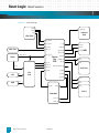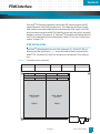
1
User’s Manual from Emerson Network Power ™ Embedded Computing Katana®752i: Intelligent CompactPCI Blade for cPSB April 2008 The information in this manual has been checked and is believed to be accurate and reliable. HOWEVER, NO RESPONSIBILITY IS ASSUMED BY EMERSON NETWORK POWER, EMBEDDED COMPUTING FOR ITS USE OR FOR ANY INACCURACIES. Specifications are subject to change without notice. EMERSON DOES NOT ASSUME ANY LIABILITY ARISING OUT OF USE OR OTHER APPLICATION OF ANY PRODUCT, CIRCUIT, OR PROGRAM DESCRIBED HEREIN. This document does not convey any license under Emerson patents or the rights of others. Emerson. Consider It Solved is a trademark, and Business-Critical Continuity, Emerson Network Power, and the Emerson Network Power logo are trademarks and service marks of Emerson Network Power, Embedded Computing, Inc. © 2008 Emerson Network Power, Embedded Computing, Inc. Revision Level: Principal Changes: Date: 10006024-00 Original release February 2006 10006024-01 Updates to page 10-4 March 2006 10006024-02 ECR01059: Added MTBF and RoHS cable info January 2007 10006024-03 Updated block diagram and FRU info July 2007 10006024-04 Updated format, Emerson contact and regulatory info, and monitor section; changed 750GX to 750GL April 2008 Copyright © 2006-2008 Emerson Network Power, Embedded Computing, Inc. All rights reserved. Regulatory Agency Warnings & Notices The Emerson Katana752i meets the requirements set forth by the Federal Communications Commission (FCC) in Title 47 of the Code of Federal Regulations. The following information is provided as required by this agency. This device complies with part 15 of the FCC Rules. Operation is subject to the following two conditions: (1) This device may not cause harmful interference, and (2) this device must accept any interference received, including interference that may cause undesired operation. FCC RULES AND REGULATIONS — PART 15 This equipment has been tested and found to comply with the limits for a Class A digital device, pursuant to part 15 of the FCC Rules. These limits are designed to provide reasonable protection against harmful interference when the equipment is operated in a commercial environment. This equipment generates, uses and can radiate radio frequency energy and, if not installed and used in accordance with the instructions, may cause harmful interference to radio communications. Operation of this equipment in a residential area is likely to cause harmful interference, in which case the user will be required to correct the interference at his own expense. Caution: Making changes or modifications to the Katana752i hardware without the explicit consent of Emerson Network Power could invalidate the user’s authority to operate this equipment. ! EMC COMPLIANCE The electromagnetic compatibility (EMC) tests used a Katana752i model that includes a front panel assembly from Emerson Network Power. Caution: For applications where the Katana752i is provided without a front panel, or where the front panel has been removed, your system chassis/enclosure must provide the required ! electromagnetic interference (EMI) shielding to maintain EMC compliance. 10006024-04 Katana®752i User’s Manual i (continued) EC Declaration of Conformity According to EN 45014:1998 Manufacturer’s Name: Emerson Network Power Embedded Computing Manufacturer’s Address: 8310 Excelsior Drive Madison, Wisconsin 53717 Declares that the following product, in accordance with the requirements of 2004/108/EEC, EMC Directive and 1999/5/EC, RTTE Directive and their amending directives, Product: Real-Time Processing Blade Model Name/Number: Katana752i/10006008-xx has been designed and manufactured to the following specifications: EN55022:1998 Information Technology Equipment, Radio disturbance characteristics, Limits and methods of measurement EN55024:1998 Information Technology Equipment, Immunity characteristics, Limits and methods of measurement EN300386 V.1.3.2:2003-05 Electromagnetic compatibility and radio spectrum matters (ERM); Telecommunication network equipment; EMC requirements As manufacturer we hereby declare that the product named above has been designed to comply with the relevant sections of the above referenced specifications. This product complies with the essential health and safety requirements of the EMC Directive and RTTE Directive. We have an internal production control system that ensures compliance between the manufactured products and the technical documentation. Bill Fleury Compliance Engineer Issue date: April 21, 2008 ii Katana®752i User’s Manual 10006024-04 Contents 1 Overview Components and Features . . . . . . . . . . . 1-1 Functional Overview . . . . . . . . . . . . . . . . 1-4 Additional Information . . . . . . . . . . . . . . 1-5 Product Certification . . . . . . . . . . . . . 1-5 RoHS Compliance. . . . . . . . . . . . . . . . 1-6 Terminology and Notation . . . . . . . . 1-6 Technical References. . . . . . . . . . . . . 1-6 2 Setup Electrostatic Discharge . . . . . . . . . . . . . . 2-1 Katana®752i Circuit Board. . . . . . . . . . . 2-1 Identification Numbers . . . . . . . . . . . 2-7 Connectors . . . . . . . . . . . . . . . . . . . . . 2-7 Fuses. . . . . . . . . . . . . . . . . . . . . . . . . . . 2-8 LEDs . . . . . . . . . . . . . . . . . . . . . . . . . . . 2-8 Katana®752i Setup . . . . . . . . . . . . . . . . . 2-9 Power Requirements . . . . . . . . . . . .2-10 Environmental Requirements . . . .2-10 Troubleshooting . . . . . . . . . . . . . . . . . . . 2-10 Technical Support . . . . . . . . . . . . . .2-11 Product Repair . . . . . . . . . . . . . . . . .2-11 3 Reset Logic General Overview . . . . . . . . . . . . . . . . . . . 3-1 Reset Sources . . . . . . . . . . . . . . . . . . . . . . 3-3 CompactPCI Reset Enable . . . . . . . . 3-3 Power Monitor . . . . . . . . . . . . . . . . . . 3-3 750GL Processor Reset . . . . . . . . . . . 3-3 Exception Processing. . . . . . . . . . . . . . . . .4-9 Cache Memory . . . . . . . . . . . . . . . . . . . . 4-11 L1 Cache . . . . . . . . . . . . . . . . . . . . . . 4-11 L2 Cache . . . . . . . . . . . . . . . . . . . . . . 4-11 JTAG/COP Headers. . . . . . . . . . . . . . . . . 4-13 5 System Controller Overview . . . . . . . . . . . . . . . . . . . . . . . . . . .5-1 CPU Interface . . . . . . . . . . . . . . . . . . . . . . .5-2 SDRAM Controller . . . . . . . . . . . . . . . . . . .5-3 Device Controller Interface. . . . . . . . . . . .5-3 Internal (IDMA) Controller . . . . . . . . . . . .5-4 Timer/Counters . . . . . . . . . . . . . . . . . . . . .5-4 PCI Interface . . . . . . . . . . . . . . . . . . . . . . . .5-4 PCI Configuration Space. . . . . . . . . . 5-4 PCI Identification . . . . . . . . . . . . . . . . 5-5 PCI Read/Write. . . . . . . . . . . . . . . . . . 5-5 PCI Interface Registers . . . . . . . . . . . 5-5 Doorbell Registers . . . . . . . . . . . . . . . . . . .5-6 Outbound Doorbells . . . . . . . . . . . . . 5-6 Inbound Doorbells. . . . . . . . . . . . . . . 5-6 Watchdog Timer . . . . . . . . . . . . . . . . . . . .5-6 Reset. . . . . . . . . . . . . . . . . . . . . . . . . . . . . . .5-6 On-Card Memory . . . . . . . . . . . . . . . . . . . .5-7 User Flash . . . . . . . . . . . . . . . . . . . . . . 5-7 SDRAM. . . . . . . . . . . . . . . . . . . . . . . . . 5-7 EEPROMs . . . . . . . . . . . . . . . . . . . . . . . 5-8 I2C Interface . . . . . . . . . . . . . . . . . . . . . . . .5-8 GPIO Signal Definitions . . . . . . . . . . . . . 5-10 Console Serial Port . . . . . . . . . . . . . . . . . 5-11 6 Device Bus PLD 4 Processor Processor Overview . . . . . . . . . . . . . . . . . 4-1 Features . . . . . . . . . . . . . . . . . . . . . . . . 4-1 Physical Memory Map . . . . . . . . . . . . 4-2 Processor Reset. . . . . . . . . . . . . . . . . . . . . 4-4 Processor Initialization. . . . . . . . . . . . . . . 4-4 Hardware Implementation Dependent 0 Register. . . . . . . . . . . . . . . . . . . . . . . . . . . . . . . 4-5 Hardware Implementation Dependent 1 Register. . . . . . . . . . . . . . . . . . . . . . . . . . . . . . . 4-6 Hardware Implementation Dependent 2 Register. . . . . . . . . . . . . . . . . . . . . . . . . . . . . . . 4-7 Exception Handling . . . . . . . . . . . . . . . . . 4-8 10006024-04 Reset Registers . . . . . . . . . . . . . . . . . . . . . .6-1 Interrupt Registers . . . . . . . . . . . . . . . . . . .6-2 Product Identification . . . . . . . . . . . . . . . .6-3 PCI Enumeration. . . . . . . . . . . . . . . . . . . . .6-3 Revision Registers . . . . . . . . . . . . . . . . . . .6-4 Board Configuration Registers. . . . . . . . .6-4 Other Registers. . . . . . . . . . . . . . . . . . . . . .6-6 7 Real-Time Clock Block Diagram. . . . . . . . . . . . . . . . . . . . . . .7-1 Operation . . . . . . . . . . . . . . . . . . . . . . . . . .7-1 Clock Operation . . . . . . . . . . . . . . . . . . . . .7-2 Katana®752i User’s Manual iii 8 Local PCI Bus PCI Enumeration. . . . . . . . . . . . . . . . . . . . .8-1 PCI ID Select and Interrupts . . . . . . . . . . .8-1 Geographical Addressing . . . . . . . . . . . . .8-2 PCI Bus Control Signals . . . . . . . . . . . . . . .8-2 9 PTMC Interface PTMC Installation . . . . . . . . . . . . . . . . . . . .9-1 PTMC Connector Pinouts . . . . . . . . . . . . .9-3 10 Ethernet Interfaces Ethernet Address . . . . . . . . . . . . . . . . . . 10-1 Ethernet Ports . . . . . . . . . . . . . . . . . . . . . 10-2 Front Panel Ethernet Connector Pinouts . . . 10-2 Optional RMII PHY Devices . . . . . . . . . . 10-3 11 IPMI Controller (blank page) SMB/IPMI Overview . . . . . . . . . . . . . . . . 11-1 I/O Interface . . . . . . . . . . . . . . . . . . . . . . 11-4 I2C Interfaces . . . . . . . . . . . . . . . . . . . . . 11-5 IPMI Message Protocol . . . . . . . . . . . . . 11-6 IPMI Network Function Codes . . . .11-8 IPMI Completion Codes . . . . . . . . .11-9 Zircon PM IPMI Commands . . . . .11-10 Get Sensor Reading (Sensor/Event) . . . 11-11 Master Write-Read I2C (Application) . . 11-14 Write Setting (OEM) . . . . . . . . . . .11-15 Read Setting (OEM) . . . . . . . . . . . .11-16 Set Heartbeat (OEM) . . . . . . . . . . .11-17 Get Heartbeat (OEM). . . . . . . . . . .11-18 IPMI FRU Information . . . . . . . . . .11-19 IPMI Device SDR Repository . . . . .11-20 IPMI Event Messages . . . . . . . . . . .11-20 12 Hot Swap Hot Swap Logic (HSL) PLD. . . . . . . . . . . 12-1 cPCI Functionality. . . . . . . . . . . . . . . . . . 12-2 Hot Swap LED and Ejector Switch Control . . 12-2 cPCI Hot Swap. . . . . . . . . . . . . . . . . .12-2 Non-cPCI Hot Swap . . . . . . . . . . . . .12-4 iv Katana®752i User’s Manual 10006024-04 Timing Considerations . . . . . . . . . . . . . 12-5 HEALTHY* Signal . . . . . . . . . . . . . . . . . . 12-6 13 CT Bus Interface PICMG 2.15 Configuration 2 . . . . . . . . 13-1 Katana®752i CT Bus Options. . . . . . . . 13-2 Clocking . . . . . . . . . . . . . . . . . . . . . . . . . . 13-2 Signal Control . . . . . . . . . . . . . . . . . . . . . 13-3 CT Bus Routing Without the T8110 (option 1). . . . . . . . . . . . . . . . . . . . . . . . . . . . . . . . . . . . 13-4 CT Bus Routing With the T8110 Installed (option 2). . . . . . . . . . . . . . . . . . . . . . . . . . . . . 13-6 Local CT Bus Operation. . . . . . . . . . 13-7 H.110 CT Bus Operation. . . . . . . . . 13-8 14 Backplane Signals Overview . . . . . . . . . . . . . . . . . . . . . . . . . 14-1 Pinouts . . . . . . . . . . . . . . . . . . . . . . . . . . . 14-2 15 Monitor Command-Line Features. . . . . . . . . . . . 15-1 Basic Operation . . . . . . . . . . . . . . . . . . . 15-3 Power-Up/Reset Sequence . . . . . . 15-3 Power-Up Timing. . . . . . . . . . . . . . . 15-5 POST Diagnostic Results . . . . . . . . 15-6 Monitor SDRAM Usage . . . . . . . . . . 15-6 Monitor Recovery and Updates . . . . . . 15-7 Recovering the Monitor . . . . . . . . . 15-7 Updating the Monitor via TFTP . . . 15-7 Resetting Environment Variables . 15-8 Monitor Command Reference . . . . . . . 15-8 Command Syntax . . . . . . . . . . . . . . 15-8 Command Help . . . . . . . . . . . . . . . . 15-9 Typographic Conventions . . . . . . . 15-9 Boot Commands . . . . . . . . . . . . . . . . . . 15-9 bootbus . . . . . . . . . . . . . . . . . . . . . . . 15-9 bootcrc . . . . . . . . . . . . . . . . . . . . . . 15-10 bootd . . . . . . . . . . . . . . . . . . . . . . . . 15-10 bootelf . . . . . . . . . . . . . . . . . . . . . . . 15-10 bootm . . . . . . . . . . . . . . . . . . . . . . . 15-10 bootp . . . . . . . . . . . . . . . . . . . . . . . . 15-10 bootv . . . . . . . . . . . . . . . . . . . . . . . . 15-11 bootvx . . . . . . . . . . . . . . . . . . . . . . . 15-11 rarpboot . . . . . . . . . . . . . . . . . . . . . 15-11 tftpboot. . . . . . . . . . . . . . . . . . . . . . 15-11 Contents (continued) JFFS2 File Systems. . . . . . . . . . . . . . . . . 15-12 ls . . . . . . . . . . . . . . . . . . . . . . . . . . . .15-12 fsinfo. . . . . . . . . . . . . . . . . . . . . . . . .15-12 fsload . . . . . . . . . . . . . . . . . . . . . . . .15-12 chpart . . . . . . . . . . . . . . . . . . . . . . . .15-12 Memory Commands . . . . . . . . . . . . . . 15-12 cmp. . . . . . . . . . . . . . . . . . . . . . . . . .15-13 cp . . . . . . . . . . . . . . . . . . . . . . . . . . .15-13 find . . . . . . . . . . . . . . . . . . . . . . . . . .15-13 md. . . . . . . . . . . . . . . . . . . . . . . . . . .15-13 mm . . . . . . . . . . . . . . . . . . . . . . . . . .15-14 nm. . . . . . . . . . . . . . . . . . . . . . . . . . .15-14 mw . . . . . . . . . . . . . . . . . . . . . . . . . .15-14 Flash Commands . . . . . . . . . . . . . . . . . 15-15 cp . . . . . . . . . . . . . . . . . . . . . . . . . . .15-15 erase . . . . . . . . . . . . . . . . . . . . . . . . .15-15 flinfo . . . . . . . . . . . . . . . . . . . . . . . . .15-15 protect . . . . . . . . . . . . . . . . . . . . . . .15-16 EEPROM / I2C Commands. . . . . . . . . . 15-16 eeprom . . . . . . . . . . . . . . . . . . . . . .15-16 icrc32 . . . . . . . . . . . . . . . . . . . . . . . .15-17 iloop . . . . . . . . . . . . . . . . . . . . . . . . .15-17 imd . . . . . . . . . . . . . . . . . . . . . . . . . .15-17 ipmifirmload . . . . . . . . . . . . . . . . . .15-17 imm . . . . . . . . . . . . . . . . . . . . . . . . .15-17 imw. . . . . . . . . . . . . . . . . . . . . . . . . .15-17 inm . . . . . . . . . . . . . . . . . . . . . . . . . .15-17 iprobe . . . . . . . . . . . . . . . . . . . . . . . .15-18 Ethernet Controller EEPROM Commands . . 15-18 initeth4rom. . . . . . . . . . . . . . . . . . .15-18 filleth4rom . . . . . . . . . . . . . . . . . . .15-18 showeth4rom . . . . . . . . . . . . . . . . .15-18 Environment Parameter Commands 15-18 envinit . . . . . . . . . . . . . . . . . . . . . . .15-19 printenv . . . . . . . . . . . . . . . . . . . . . .15-19 saveenv . . . . . . . . . . . . . . . . . . . . . .15-19 setenv. . . . . . . . . . . . . . . . . . . . . . . .15-19 Test Commands . . . . . . . . . . . . . . . . . . 15-20 diags . . . . . . . . . . . . . . . . . . . . . . . . .15-20 mtest . . . . . . . . . . . . . . . . . . . . . . . .15-20 um. . . . . . . . . . . . . . . . . . . . . . . . . . .15-20 Other Commands. . . . . . . . . . . . . . . . . 15-20 autoscr . . . . . . . . . . . . . . . . . . . . . . .15-20 base . . . . . . . . . . . . . . . . . . . . . . . . .15-20 10006024-04 bdinfo . . . . . . . . . . . . . . . . . . . . . . . 15-20 coninfo . . . . . . . . . . . . . . . . . . . . . . 15-21 crc16 . . . . . . . . . . . . . . . . . . . . . . . . 15-21 crc32 . . . . . . . . . . . . . . . . . . . . . . . . 15-21 echo . . . . . . . . . . . . . . . . . . . . . . . . . 15-21 enumpci . . . . . . . . . . . . . . . . . . . . . 15-21 fpledoff . . . . . . . . . . . . . . . . . . . . . . 15-21 fruget. . . . . . . . . . . . . . . . . . . . . . . . 15-21 frugetuser . . . . . . . . . . . . . . . . . . . . 15-21 frusetuser . . . . . . . . . . . . . . . . . . . . 15-22 gethvr . . . . . . . . . . . . . . . . . . . . . . . 15-22 getmonver . . . . . . . . . . . . . . . . . . . 15-22 getpcimemsize . . . . . . . . . . . . . . . 15-22 getpcimode . . . . . . . . . . . . . . . . . . 15-23 getphysloc . . . . . . . . . . . . . . . . . . . 15-23 getspr . . . . . . . . . . . . . . . . . . . . . . . 15-23 go . . . . . . . . . . . . . . . . . . . . . . . . . . . 15-23 help . . . . . . . . . . . . . . . . . . . . . . . . . 15-23 iminfo . . . . . . . . . . . . . . . . . . . . . . . 15-23 isdram . . . . . . . . . . . . . . . . . . . . . . . 15-24 loop . . . . . . . . . . . . . . . . . . . . . . . . . 15-24 memmap . . . . . . . . . . . . . . . . . . . . 15-24 moninit . . . . . . . . . . . . . . . . . . . . . . 15-24 pci. . . . . . . . . . . . . . . . . . . . . . . . . . . 15-24 reset . . . . . . . . . . . . . . . . . . . . . . . . . 15-25 run . . . . . . . . . . . . . . . . . . . . . . . . . . 15-25 setpcimemsize. . . . . . . . . . . . . . . . 15-25 setpcimode. . . . . . . . . . . . . . . . . . . 15-25 setspr . . . . . . . . . . . . . . . . . . . . . . . . 15-26 script . . . . . . . . . . . . . . . . . . . . . . . . 15-26 showmac. . . . . . . . . . . . . . . . . . . . . 15-26 showpci . . . . . . . . . . . . . . . . . . . . . . 15-26 showtemp. . . . . . . . . . . . . . . . . . . . 15-26 sleep. . . . . . . . . . . . . . . . . . . . . . . . . 15-26 vdhcp . . . . . . . . . . . . . . . . . . . . . . . . 15-26 version . . . . . . . . . . . . . . . . . . . . . . . 15-27 Environment Variables . . . . . . . . . . . . 15-27 Troubleshooting. . . . . . . . . . . . . . . . . . 15-30 Download Formats. . . . . . . . . . . . . . . . 15-30 Binary. . . . . . . . . . . . . . . . . . . . . . . . 15-30 Motorola S-Record . . . . . . . . . . . . 15-30 16 Acronyms Katana®752i User’s Manual v (blank page) vi Katana®752i User’s Manual 10006024-04 Figures Figure 1-1: General System Block Diagram. . . . . . . . . . . . . . . . . . . . . . . . . . . . . . . . . . . . . . . . . . . . . . 1-4 Figure 2-1: Katana®752i Front Panel. . . . . . . . . . . . . . . . . . . . . . . . . . . . . . . . . . . . . . . . . . . . . . . . . . . 2-2 Figure 2-2: Component Map, Top (Rev. 03) . . . . . . . . . . . . . . . . . . . . . . . . . . . . . . . . . . . . . . . . . . . . . 2-3 Figure 2-3: Component Map, Bottom (Rev. 03). . . . . . . . . . . . . . . . . . . . . . . . . . . . . . . . . . . . . . . . . . 2-4 Figure 2-4: Jumper, Fuse, and Switch Locations, Top . . . . . . . . . . . . . . . . . . . . . . . . . . . . . . . . . . . . . 2-5 Figure 2-5: Fuse, and LED Locations, Bottom . . . . . . . . . . . . . . . . . . . . . . . . . . . . . . . . . . . . . . . . . . . . 2-6 Figure 3-1: Katana®752i Reset Diagram. . . . . . . . . . . . . . . . . . . . . . . . . . . . . . . . . . . . . . . . . . . . . . . . 3-2 Figure 3-2: 750GL Reset Logic . . . . . . . . . . . . . . . . . . . . . . . . . . . . . . . . . . . . . . . . . . . . . . . . . . . . . . . . . 3-4 Figure 4-1: 750GL Block Diagram . . . . . . . . . . . . . . . . . . . . . . . . . . . . . . . . . . . . . . . . . . . . . . . . . . . . . . 4-2 Figure 4-2: 750GL Memory Map . . . . . . . . . . . . . . . . . . . . . . . . . . . . . . . . . . . . . . . . . . . . . . . . . . . . . . . 4-3 Figure 5-1: MV64460 Block Diagram . . . . . . . . . . . . . . . . . . . . . . . . . . . . . . . . . . . . . . . . . . . . . . . . . . . 5-2 Figure 5-2: I2C Interface Diagram. . . . . . . . . . . . . . . . . . . . . . . . . . . . . . . . . . . . . . . . . . . . . . . . . . . . . . 5-9 Figure 5-3: Standard Console Cable Wiring, #10007665-00 . . . . . . . . . . . . . . . . . . . . . . . . . . . . . . 5-11 Figure 7-1: M41T00 Real-Time Clock Block Diagram . . . . . . . . . . . . . . . . . . . . . . . . . . . . . . . . . . . . . 7-1 Figure 9-1: PTMC Module Location on Baseboard . . . . . . . . . . . . . . . . . . . . . . . . . . . . . . . . . . . . . . . . 9-1 Figure 10-1: RMII PHY to Transition Module . . . . . . . . . . . . . . . . . . . . . . . . . . . . . . . . . . . . . . . . . . . . . 10-4 Figure 11-1: IPMB Connections Block Diagram . . . . . . . . . . . . . . . . . . . . . . . . . . . . . . . . . . . . . . . . . . 11-3 Figure 12-1: Hot Swap Controller Circuit. . . . . . . . . . . . . . . . . . . . . . . . . . . . . . . . . . . . . . . . . . . . . . . . 12-4 Figure 13-1: Typical System Clocking Model . . . . . . . . . . . . . . . . . . . . . . . . . . . . . . . . . . . . . . . . . . . . 13-3 Figure 13-2: CT Signal Routing Diagram —T8110 Not Installed (option 1) . . . . . . . . . . . . . . . . . . . 13-5 Figure 13-3: CT Signal Routing Diagram —T8110 Installed (option 2) . . . . . . . . . . . . . . . . . . . . . . . 13-8 Figure 14-1: cPCI Connector Pin Assignments, J5 . . . . . . . . . . . . . . . . . . . . . . . . . . . . . . . . . . . . . . . . 14-6 Figure 15-1: Example Monitor Start-up Display . . . . . . . . . . . . . . . . . . . . . . . . . . . . . . . . . . . . . . . . . . 15-2 Figure 15-2: Power-up/Reset Sequence Flowchart . . . . . . . . . . . . . . . . . . . . . . . . . . . . . . . . . . . . . . . 15-4 10006024-04 Katana®752i User’s Manual vii (blank page) viii Katana®752i User’s Manual 10006024-04 Tables Table 1-1: Regulatory Agency Compliance . . . . . . . . . . . . . . . . . . . . . . . . . . . . . . . . . . . . . . . . . . . . . 1-5 Table 1-2: Technical References . . . . . . . . . . . . . . . . . . . . . . . . . . . . . . . . . . . . . . . . . . . . . . . . . . . . . . 1-7 Table 2-1: Circuit Board Dimensions . . . . . . . . . . . . . . . . . . . . . . . . . . . . . . . . . . . . . . . . . . . . . . . . . . 2-1 Table 2-2: LEDs . . . . . . . . . . . . . . . . . . . . . . . . . . . . . . . . . . . . . . . . . . . . . . . . . . . . . . . . . . . . . . . . . . . . . 2-8 Table 4-1: Katana®752i CPU Features . . . . . . . . . . . . . . . . . . . . . . . . . . . . . . . . . . . . . . . . . . . . . . . . . 4-1 Table 4-2: Katana®752i Address Summary . . . . . . . . . . . . . . . . . . . . . . . . . . . . . . . . . . . . . . . . . . . . 4-4 Table 4-3: CPU Internal Register Initialization. . . . . . . . . . . . . . . . . . . . . . . . . . . . . . . . . . . . . . . . . . . 4-4 Table 4-4: 750GL Exception Priorities. . . . . . . . . . . . . . . . . . . . . . . . . . . . . . . . . . . . . . . . . . . . . . . . . . 4-8 Table 4-5: Floating Point Exception Mode Bits . . . . . . . . . . . . . . . . . . . . . . . . . . . . . . . . . . . . . . . . . 4-10 Table 4-6: 750GL JTAG/COP Interface Pin Assignments, (P3) . . . . . . . . . . . . . . . . . . . . . . . . . . . . 4-13 Table 5-1: PCI Identification Values . . . . . . . . . . . . . . . . . . . . . . . . . . . . . . . . . . . . . . . . . . . . . . . . . . . 5-5 Table 5-2: NVRAM Allocation . . . . . . . . . . . . . . . . . . . . . . . . . . . . . . . . . . . . . . . . . . . . . . . . . . . . . . . . . 5-8 Table 5-3: GPIO Signals Definitions. . . . . . . . . . . . . . . . . . . . . . . . . . . . . . . . . . . . . . . . . . . . . . . . . . . 5-10 Table 5-4: Serial Console Port Pin Assignments, (P2) . . . . . . . . . . . . . . . . . . . . . . . . . . . . . . . . . . . 5-11 Table 7-1: RTC Register Map . . . . . . . . . . . . . . . . . . . . . . . . . . . . . . . . . . . . . . . . . . . . . . . . . . . . . . . . . 7-2 Table 8-1: ID Select Connections. . . . . . . . . . . . . . . . . . . . . . . . . . . . . . . . . . . . . . . . . . . . . . . . . . . . . . 8-2 Table 8-2: Interrupt Connections for Katana®752i . . . . . . . . . . . . . . . . . . . . . . . . . . . . . . . . . . . . . . 8-2 Table 8-3: Geographical Address Registers . . . . . . . . . . . . . . . . . . . . . . . . . . . . . . . . . . . . . . . . . . . . . 8-2 Table 9-1: J1x PTMC Connector Pin Assignments. . . . . . . . . . . . . . . . . . . . . . . . . . . . . . . . . . . . . . . . 9-3 Table 9-2: J2x PTMC Connector Pin Assignments. . . . . . . . . . . . . . . . . . . . . . . . . . . . . . . . . . . . . . . . 9-5 Table 10-1: GbE Port LEDs. . . . . . . . . . . . . . . . . . . . . . . . . . . . . . . . . . . . . . . . . . . . . . . . . . . . . . . . . . . . 10-2 Table 10-2: 82544EI Ethernet Port Pin Assignments, ETH4 . . . . . . . . . . . . . . . . . . . . . . . . . . . . . . . 10-3 Table 10-3: MV64460 Ethernet Port Pin Assignments, ETH3 . . . . . . . . . . . . . . . . . . . . . . . . . . . . . . 10-3 Table 10-4: PTMC PHY Address . . . . . . . . . . . . . . . . . . . . . . . . . . . . . . . . . . . . . . . . . . . . . . . . . . . . . . . 10-3 Table 11-1: Zircon PM General Purpose I/O Pin Functions . . . . . . . . . . . . . . . . . . . . . . . . . . . . . . . . 11-4 Table 11-2: Zircon PM Analog-to-Digital Input Pin Functions . . . . . . . . . . . . . . . . . . . . . . . . . . . . . 11-5 Table 11-3: IPMB Slave Addresses . . . . . . . . . . . . . . . . . . . . . . . . . . . . . . . . . . . . . . . . . . . . . . . . . . . . . 11-6 Table 11-4: Format for IPMI Request Message . . . . . . . . . . . . . . . . . . . . . . . . . . . . . . . . . . . . . . . . . . 11-6 Table 11-5: Format for IPMI Response Message . . . . . . . . . . . . . . . . . . . . . . . . . . . . . . . . . . . . . . . . . 11-7 Table 11-6: Network Function Codes . . . . . . . . . . . . . . . . . . . . . . . . . . . . . . . . . . . . . . . . . . . . . . . . . . 11-8 Table 11-7: Completion Codes. . . . . . . . . . . . . . . . . . . . . . . . . . . . . . . . . . . . . . . . . . . . . . . . . . . . . . . . 11-9 Table 11-8: Zircon PM IPMI Commands . . . . . . . . . . . . . . . . . . . . . . . . . . . . . . . . . . . . . . . . . . . . . . . 11-10 Table 11-9: Get Sensor Reading Parameters . . . . . . . . . . . . . . . . . . . . . . . . . . . . . . . . . . . . . . . . . . . 11-12 Table 11-10: Master Write-Read I2C Parameters . . . . . . . . . . . . . . . . . . . . . . . . . . . . . . . . . . . . . . . . 11-14 Table 11-11: Write Setting Parameters. . . . . . . . . . . . . . . . . . . . . . . . . . . . . . . . . . . . . . . . . . . . . . . . . 11-15 Table 11-12: Read Setting Parameters . . . . . . . . . . . . . . . . . . . . . . . . . . . . . . . . . . . . . . . . . . . . . . . . . 11-16 Table 11-13: Set Heartbeat Parameters . . . . . . . . . . . . . . . . . . . . . . . . . . . . . . . . . . . . . . . . . . . . . . . . 11-17 Table 11-14: Get Heartbeat Parameters. . . . . . . . . . . . . . . . . . . . . . . . . . . . . . . . . . . . . . . . . . . . . . . . 11-18 Table 11-15: FRU Definition . . . . . . . . . . . . . . . . . . . . . . . . . . . . . . . . . . . . . . . . . . . . . . . . . . . . . . . . . . 11-19 Table 11-16: IPMI Event Messages Generating Sensors. . . . . . . . . . . . . . . . . . . . . . . . . . . . . . . . . . . 11-20 10006024-04 Katana®752i User’s Manual ix Tables x (continued) Katana®752i User’s Manual Table 11-17: Event Message Format . . . . . . . . . . . . . . . . . . . . . . . . . . . . . . . . . . . . . . . . . . . . . . . . . . . 11-20 Table 11-18: System Firmware Progress OEM Event Data . . . . . . . . . . . . . . . . . . . . . . . . . . . . . . . . 11-21 Table 12-1: HSL PLD Register Summary . . . . . . . . . . . . . . . . . . . . . . . . . . . . . . . . . . . . . . . . . . . . . . . . 12-1 Table 13-1: CT Clock Control Registers . . . . . . . . . . . . . . . . . . . . . . . . . . . . . . . . . . . . . . . . . . . . . . . . 13-3 Table 13-2: Local CT Bus Bit Map . . . . . . . . . . . . . . . . . . . . . . . . . . . . . . . . . . . . . . . . . . . . . . . . . . . . . . 13-6 Table 14-1: cPCI Connector Pin Assignments, J1 . . . . . . . . . . . . . . . . . . . . . . . . . . . . . . . . . . . . . . . . 14-2 Table 14-2: cPCI Connector Pin Assignments, J2 . . . . . . . . . . . . . . . . . . . . . . . . . . . . . . . . . . . . . . . . 14-3 Table 14-3: cPSB Connector Pin Assignments, J3 . . . . . . . . . . . . . . . . . . . . . . . . . . . . . . . . . . . . . . . . 14-4 Table 14-4: cPSB Connector Pin Assignments, J4 . . . . . . . . . . . . . . . . . . . . . . . . . . . . . . . . . . . . . . . . 14-5 Table 15-1: Power-Up Timing for Booting from Soldered Flash. . . . . . . . . . . . . . . . . . . . . . . . . . . . 15-5 Table 15-2: Power-Up Timing for Booting from Socketed Flash . . . . . . . . . . . . . . . . . . . . . . . . . . . 15-5 Table 15-3: POST Diagnostics Results. . . . . . . . . . . . . . . . . . . . . . . . . . . . . . . . . . . . . . . . . . . . . . . . . . 15-6 Table 15-4: Standard Environment Variables . . . . . . . . . . . . . . . . . . . . . . . . . . . . . . . . . . . . . . . . . . 15-27 Table 15-5: Optional Environment Variables. . . . . . . . . . . . . . . . . . . . . . . . . . . . . . . . . . . . . . . . . . . 15-29 10006024-04 Registers Register 4-1: 750GL Hardware Implementation Dependent, HID0. . . . . . . . . . . . . . . . . . . . . . . . . . . 4-5 Register 4-2: 750GL Hardware Implementation Dependent, HID1. . . . . . . . . . . . . . . . . . . . . . . . . . . 4-6 Register 4-3: 750GL Hardware Implementation Dependent, HID2. . . . . . . . . . . . . . . . . . . . . . . . . . . 4-7 Register 4-4: CPU Machine State (MSR) . . . . . . . . . . . . . . . . . . . . . . . . . . . . . . . . . . . . . . . . . . . . . . . . . . 4-9 Register 4-5: L2 Cache Control Register (L2CR). . . . . . . . . . . . . . . . . . . . . . . . . . . . . . . . . . . . . . . . . . . 4-11 Register 6-1: Reset Event . . . . . . . . . . . . . . . . . . . . . . . . . . . . . . . . . . . . . . . . . . . . . . . . . . . . . . . . . . . . . . . 6-1 Register 6-2: Reset Command . . . . . . . . . . . . . . . . . . . . . . . . . . . . . . . . . . . . . . . . . . . . . . . . . . . . . . . . . . 6-2 Register 6-3: Interrupt Enable. . . . . . . . . . . . . . . . . . . . . . . . . . . . . . . . . . . . . . . . . . . . . . . . . . . . . . . . . . . 6-2 Register 6-4: Interrupt Pending . . . . . . . . . . . . . . . . . . . . . . . . . . . . . . . . . . . . . . . . . . . . . . . . . . . . . . . . . 6-3 Register 6-5: Product ID . . . . . . . . . . . . . . . . . . . . . . . . . . . . . . . . . . . . . . . . . . . . . . . . . . . . . . . . . . . . . . . . 6-3 Register 6-6: EReady . . . . . . . . . . . . . . . . . . . . . . . . . . . . . . . . . . . . . . . . . . . . . . . . . . . . . . . . . . . . . . . . . . . 6-4 Register 6-7: Hardware Version . . . . . . . . . . . . . . . . . . . . . . . . . . . . . . . . . . . . . . . . . . . . . . . . . . . . . . . . . 6-4 Register 6-8: PLD Version. . . . . . . . . . . . . . . . . . . . . . . . . . . . . . . . . . . . . . . . . . . . . . . . . . . . . . . . . . . . . . . 6-4 Register 6-9: Board Configuration 3. . . . . . . . . . . . . . . . . . . . . . . . . . . . . . . . . . . . . . . . . . . . . . . . . . . . . . 6-5 Register 6-10: Board Configuration 1 . . . . . . . . . . . . . . . . . . . . . . . . . . . . . . . . . . . . . . . . . . . . . . . . . . . . . 6-5 Register 6-11: Board Configuration 0 . . . . . . . . . . . . . . . . . . . . . . . . . . . . . . . . . . . . . . . . . . . . . . . . . . . . . 6-5 Register 6-12: IPMI Port Select . . . . . . . . . . . . . . . . . . . . . . . . . . . . . . . . . . . . . . . . . . . . . . . . . . . . . . . . . . . 6-6 Register 6-13: Programmable LED . . . . . . . . . . . . . . . . . . . . . . . . . . . . . . . . . . . . . . . . . . . . . . . . . . . . . . . . 6-6 Register 10-1: MAC Calculation . . . . . . . . . . . . . . . . . . . . . . . . . . . . . . . . . . . . . . . . . . . . . . . . . . . . . . . . . 10-1 10006024-04 Katana®752i User’s Manual i (blank page) ii Katana®752i User’s Manual 10006024-04 Section 1 Overview The Emerson Katana® 752i is an intelligent input/output (I/O) processing blade for use in a CompactPCI backplane. It is compatible with the CompactPCI Packet-Switched Backplane (cPSB) and has two PCI Telecom Mezzanine Card (PTMC) sites that can support two telecommunications interface cards, such as the Emerson PM/3Gv. The Katana®752i draws processing power from its IBM PowerPC® 750GL microprocessor, running at a speed of up to 1GHz. A Marvell system controller serves as a PCI bridge. In the standard configuration, the Katana®752i connects two Gigabit Ethernet ports to the front panel and two Gigabit Ethernet ports to the J3 backplane connector, which (depending upon the configuration) provides access to a rear transition module or cPSB. The Katana®752i supports various memory configurations, user Flash memory, a front-panel serial port, and user I/O from the PTMC sites. Optionally, the Katana®752i supports the H.110 Computer Telephony (CT) bus and various clocking signals. COMPONENTS AND FEATURES The following is a brief summary of the Katana®752i hardware components and features: CPU: The Katana®752i features an IBM 750GL central processing unit (CPU), operating at a rate of up to 1GHz. The CPU is a 32-bit PowerPC RISC microprocessor with 32-kilobyte, Level-1, data and instruction caches, as well as a one-megabyte, four-way, set-associative, Level-2 cache. System Controller/PCI Bridge: The Katana®752i employs a system controller/PCI bridge device from Marvell. The Discovery™ III MV64460 is a single-chip solution that provides a high-speed (up to 200MHz) 60x bus interface, double-data rate (DDR) SDRAM controller, two 66-MHz PCI interfaces (64 bits for CompactPCI, 32 bits for PTMC sites), three 10/100/1000BaseT Ethernet MAC controllers, two multi-protocol serial controllers (MPSC), an interrupt controller, and 32 general-purpose input/output (I/O) signals. The MV64460 also includes an inter-integrated circuit (I2C) interface. 10006024-04 Katana®752i User’s Manual 1-1 Overview: Components and Features SDRAM: The Katana®752i allows for a 72-bit Small-Outline Dual In-Line Memory Module (SODIMM) of up to two gigabytes to support the CPU. (Please contact Emerson for the availability of one- and two-gigabyte SO-DIMMs.) This SDRAM operates at a speed of up to 200 MHz and has Error Checking and Correction (ECC) code. Flash: The Katana®752i supports up to 128 megabytes soldered user Flash memory for the CPU. The Flash bank is 32 bits wide, using two or four 16-bit wide devices. The Katana®752i also supports 512 kilobytes of socketed Flash. The Flash memory conforms to the Intel StrataFlash™ architecture. The CPU is capable of booting from either Flash memory. H.110: The Katana®752i has an optional configuration that supports the H.110 Computer Telephony (CT) bus in accordance with the PICMG 2.5 Computer Telephony Specification and ECTF H.110 Specification, and it complies with Configuration 2 of the PICMG 2.15 PCI Telecom Mezzanine/Carrier Card Specification. The optional Agere Systems T8110 Time Slot Interchanger (TSI) serves as a bridge between the H.110 and local CT bus. Ethernet Ports: The Katana®752i provides four, 10/100/1000BaseT, Gigabit Media-Independent Interface (GMII) Ethernet ports (three from the MV64460 system controller, one from the 82544EI Ethernet controller). Two ports route to the front panel RJ45 connectors, and two ports route to the J3 CompactPCI (cPCI) connector for use either by a rear transition module or a cPCI packet-switched backplane (cPSB). Four PHY devices (three Broadcom BCM5461S, one Intel 82544EI) provide the physical interface for these ports. Optionally, the Katana®752i can support two Reduced Media-Independent (RMII) 10/100BaseT Ethernet ports routed from the PTMC sites to connector J5. Two Micrel KS8721CL PHYs support these ports. Serial I/O: The MV64460 system controllers provides an asynchronous console serial port, which supports EIA-232 signal levels. This serial port is accessible via a mini-DB9 connector on the Katana®752i front panel and the backplane connector J5. CT Bus Clocks: Optionally, the Katana®752i can provide computer telephony (CT) bus clocking. One option supports only the CT clocks (C8A, C8B, FRAMEA, FRAMEB, NETREF1, and NETFER2) between J4 and the PTMC sites. A second option supports CT bus clocking plus CT data traffic via an Agere Systems T8110 Time Slot Interchanger (TSI). This routes H.110 to the backplane connector J4. 1-2 Katana®752i User’s Manual 10006024-04 Overview: Components and Features PTMC Sites: The Katana®752i has two standard PCI Telecom Mezzanine Card (PTMC) slots, which allow for the use of two compatible PTMC boards, such as the Emerson PM/3Gv telecommunications interface card. (Refer to the PM/3Gv User’s Manual for details on the PM/3Gv.) The Katana®752i complies with Configuration 2 of the PCI Telecom Mezzanine/Carrier Card Specification, PICMG 2.15. IPMI: The Katana®752i supports an Intelligent Platform Management Interface (IPMI) by using a Zircon PM controller device from QLogic Corporation. Rear Transition Module: An optional TmPIM rear transition module (RTM) can host two PCI Mezzanine Card Input/Output Modules (PIMs). This RTM routes input/output signals from the Katana®752i PMC slots to the PIM slots. It can also route two Ethernet ports and an EIA-232 serial port from the J3 backplane connector to its rear panel. The Katana®752i also supports the TM/cSpan-P16 and TM/cSpan-P8E RTMs from Emerson. See the appropriate RTM user manuals more information. 10006024-04 Katana®752i User’s Manual 1-3 32/64/128 MB Flash 512KB Socketed Flash μDB-9 RS232 RJ45 RJ45 1000BaseT 1000BaseT MAG PMC Site #1 32 bit/33/66MHz PCI 64 User I/O CT Bus per PT2MC PMC Site #2 J14 J13 J22 J21 J24 J23 Opt. Opt. KS8721CL KS8721CL J5 I/O User I/O MAG BCM 5461S 32 bit/33/66MHz PCI 64 User I/O CT Bus per PT2MC J11 Opt. TSI T8110 J12 Clock Buffer RMII GbE MAC/PHY PCI MAG MAG BCM BCM 5461S 5461S CT Bus Clocks J3 cPSB & I/O Opt J4 H.110 RMII Marvell D-III System Controller J2 User I/O IBM 750GX CPCI 256/512MB 1GB/2GB DDR SDRAM GMII 1.5V NVRAM RTC 3.3V Power Supply & Monitoring Power Voltage Monitors Temp Sensors FRU ROM Switch IPMI CTRL J1 2.5V PTMCEthernet 1000BaseT PCI RS232 I2C CT Bus 10006024-04 Katana®752i User’s Manual 1-4 Functional Overview Overview: FUNCTIONAL OVERVIEW The following block diagram provides a functional overview for the Katana®752i. Figure 1-1: General System Block Diagram Overview: Additional Information ADDITIONAL INFORMATION This section lists the Katana®752i hardware’s regulatory certifications and briefly discusses the terminology and notation conventions used in this manual. It also lists general technical references. Mean time between failures (MTBF) has been calculated at 500,674 hours using Telcordia SR-232, Issue 1, Reliability Prediction for Electronic Equipment at 40°C. Product Certification The Katana®752i hardware has been tested to comply with various safety, immunity, and emissions requirements as specified by the Federal Communications Commission (FCC), Underwriters Laboratories (UL), and others. The following table summarizes this compliance. Table 1-1: Regulatory Agency Compliance Type: Specification: Safety IEC60950/EN60950 – Safety of Information Technology Equipment (Western Europe) UL60950, CSA C22.2 No. 60950, Third Edition – Safety of Information Technology Equipment, including Electrical Business Equipment (BI-National) Global IEC – CB Scheme Report IEC 60950, all country deviations Environmental NEBS: Telecordia GR-63 – Section 4.1.1 Transportation and Storage Environmental Criteria; Section 4.3 Equipment Handling Criteria; Section 4.4.1 Earthquake Environment and Criteria; Section 4.4.3 Office Vibration Environment and Criteria; Section 4.4.4 Transportation Vibration Criteria Section 4.5 Airborne Contaminants EMC FCC Part 15, Class A – Title 47, Code of Federal Regulations, Radio Frequency Devices ICES 003, Class A – Radiated and Conducted Emissions, Canada NEBS: Telecordia GR-1089 level 3 – Emissions and Immunity (circuit pack level testing only) ETSI EN300386 – Electromagnetic Compatibility and Radio Spectrum Matters (ERM), Telecommunication Network Equipment, Electromagnetic Compatibility (EMC) Requirements 10006024-04 Katana®752i User’s Manual 1-5 Overview: Additional Information Emerson maintains test reports that provide specific information regarding the methods and equipment used in compliance testing. Unshielded external I/O cables, loose screws, or a poorly grounded chassis may adversely affect the Katana®752i hardware’s ability to comply with any of the stated specifications. The UL web site at ul.com has a list of Emerson’s UL certifications. To find the list, search in the online certifications directory using Emerson’s UL file number, E190079. There is a list for products distributed in the United States, as well as a list for products shipped to Canada. To find the Katana®752i, search in the list for 10006008-xx, where xx changes with each revision of the printed circuit board. RoHS Compliance The Katana®752i is compliant with the European Union’s RoHS (Restriction of Use of Hazardous Substances) directive, created to limit harm to the environment and human health by restricting the use of harmful substances in electrical and electronic equipment. Effective July 1, 2006, RoHS restricts the use of six substances: cadmium (Cd), mercury (Hg), hexavalent chromium (Cr (VI)), polybrominated biphenyls (PBBs), polybrominated diphenyl ethers (PBDEs), and lead (Pb). Configurations that are RoHS compliant are built with lead-free solder. Configurations that are 5-of-6 are built with tin-lead solder per the lead-insolder RoHS exemption. To obtain a certificate of conformity (CoC) for the Katana®752i, send an e-mail to [email protected] or call 1-800-356-9602. Please have the part number(s) (e.g., C000####-##) for your configuration(s) available when contacting Emerson. Terminology and Notation Active low signals: An active low signal is indicated with an asterisk * after the signal name. Byte, word: Throughout this manual byte refers to 8 bits, word refers to 16 bits, and long word refers to 32 bits, double long word refers to 64 bits. PLD: This manual uses the acronym, PLD, as a generic term for programmable logic device (also known as FPGA, CPLD, EPLD, etc.). Radix 2 and 16: Hexadecimal numbers end with a subscript 16. Binary numbers are shown with a subscript 2. Technical References Further information on basic operation and programming of the Katana®752i components can be found in the following documents. 1-6 Katana®752i User’s Manual 10006024-04 Overview: Additional Information Table 1-2: Technical References Device/Interface: Type: Document: 1 CompactPCI® Specification (PCI Industrial Computers Manufacturers Group, PICMG® 2.0 R3.0, Oct. 1, 1999) CompactPCI Hot Swap Specification (PICMG® 2.1 R2.0, Jan. 17, 2001) System Management Specification (PICMG® 2.9 R1.0, Feb. 2, 2000) PCI Telecom Mezzanine/Carrier Card Specification (PICMG® 2.15 R1.0, Apr. 11, 2001) Packet Switching Backplane Specification (PICMG® 2.16 R1.0, Sept. 5, 2001) CPU 750GL http://www.picmg.org IBM PowerPC™ 750GX and 750GL RISC Microprocessor User’s Manual (IBM Corporation, Version 1.2, March 27, 2006) IBM PowerPC™ 750GL RISC Microprocessor Revision Level DD1.X Datasheet (IBM Corporation, Preliminary, Version 1.2, March 13, 2006) ™ PowerPC Microprocessor Family: The Programming Environments for 32-Bit Microprocessors (IBM Corporation, G522-0290-01) ™ PowerPC Microprocessor Family: The Bus Interface for 32-Bit Microprocessors (IBM Corporation, G522-0291-00) http://www.ibm.com 10006024-04 Katana®752i User’s Manual 1-7 Overview: Additional Information Device/Interface: Type: Document: 1 Ethernet BCM5461S BCM5461S 10/100/1000Base-T Gigabit Ethernet Transceiver Advance Data Sheet (Broadcom Corp., 5461S-DS04-R, April 27, 2004) (continued) http://www.broadcom.com 82544EI 82544EI Gigabit Ethernet Controller Datasheet and Hardware Design Guide; Application Note (AP-422) (Intel Corp., Doc. No. A44740-005, Rev. 0.80, Dec. 2003) http://www.intel.com KS8721CL KS8721CL 3.3V Single Power Supply 10/100BASE-TX/FX MII Physical Layer Transceiver Data Sheet, Rev. 1.2 (Micrel, Inc., M9999-041405, April 2005) http://www.micrel.com IEEE Standard for Information Technology: IEEE Std 802.3, 2000 Edition (IEEE: New York, NY) http://www.ieee.org Hot Swap Controller LTC1643L LTC1643L/LTC1643L-1/LTC1643H PCI-Bus Hot Swap Controller Data Sheet (Linear Technology Corp., 1998) http://www.linear.com IPMI/IPMB IPMI — Intelligent Platform Management Interface Specification v1.5 (Intel Corp., Hewlett-Packard Co., NEC Corp., Dell Computer Corp., Rev. 1.1, Feb. 20, 2002) IPMI — Intelligent Platform Management Bus Communications Protocol Specification v1.0 (Intel Corp., Hewlett-Packard Co., NEC Corp., Dell Computer Corp., Rev. 1.0, Sept. 16, 1998) http://www.intel.com/design/servers/ipmi/spec.htm IPMI Controller Zircon PM Zircon PM Technical Manual (QLogic Corp., 36000-510-03, Rev. C, Apr. 2002) http://www.qlogic.com PCI PCI Local Bus Specification (PCI Special Interest Group, Revision 2.3, March 29, 2002) http://www.pcisig.com PMC IEEE Standard for a Common Mezzanine Card (CMC) Family: IEEE Std 1386-2001 (IEEE: New York, NY) IEEE Standard for Physical and Environmental Layers for PCI Mezzanine Cards: IEEE Std 1386.1-2001 (IEEE: New York, NY) http://www.ieee.org 1-8 Katana®752i User’s Manual 10006024-04 Overview: Additional Information Device/Interface: Type: Document: 1 H.110 T8110 Ambassador® T8110 PCI-Based H.100/H.110 Switch and Packet Payload Engine (Agere Systems, April 2001 AY01-021CT1) (continued) http://www.agere.com H.110 Hardware Compatibility Specification: CT Bus (ECTF, revision 1.0) http://www.ectf.org Serial Interface EIA-232-F TIA/EIA-232-F: Interface Between Data Terminal Equipment and Data Circuit-Terminating Equipment Employing Serial Binary Data Interchange (Electronic Industries Association, October 1997) System Controller MV64460 PTMC Module PM/3Gv Transition Module TmPIM TM/cSpan-P16 TM/cSpan-P8E http://www.eia.com/ MV6446x System Controller for PowerPC Processors (Marvell, MV-S101286-01, Rev. A, June 19, 2003) http://www.marvell.com PM/3Gv User’s Manual (Emerson Network Power, Embedded Computing #10003035-xx) http://www.emersonembeddedcomputing.com TmPIM User’s Manual (Emerson Network Power, Embedded Computing #10005691-xx) TM/cSpan-P16 User’s Manual (Emerson Network Power, Embedded Computing #10001320-xx) TM/cSpan-P8E User’s Manual (Emerson Network Power, Embedded Computing #10005363-xx) http://www.emersonembeddedcomputing.com 1. Frequently, the most current information regarding addenda/errata for specific documents may be found on the corresponding web site. If you have questions, please call Emerson Technical Support at 1-800-327-1251, visit the web site at http://www.emersonembeddedcomputing.com, or send e-mail to [email protected]. 10006024-04 Katana®752i User’s Manual 1-9 (blank page) 1-10 Katana®752i User’s Manual 10006024-04 Section 2 Setup This chapter describes the physical layout of the boards, the setup process, and how to check for proper operation once the boards have been installed. This chapter also includes troubleshooting, service, and warranty information. ELECTROSTATIC DISCHARGE Before you begin the setup process, please remember that electrostatic discharge (ESD) can easily damage the components on the Katana®752i hardware. Electronic devices, especially those with programmable parts, are susceptible to ESD, which can result in operational failure. Unless you ground yourself properly, static charges can accumulate in your body and cause ESD damage when you touch the board. Caution: Use proper static protection and handle Katana®752i boards only when absolutely necessary. Always wear a wriststrap to ground your body before touching a board. Keep ! your body grounded while handling the board. Hold the board by its edges–do not touch any components or circuits. When the board is not in an enclosure, store it in a staticshielding bag. To ground yourself, wear a grounding wriststrap. Simply placing the board on top of a static-shielding bag does not provide any protection–place it on a grounded dissipative mat. Do not place the board on metal or other conductive surfaces. KATANA®752I CIRCUIT BOARD The Katana®752i circuit board is a 6U CompactPCI card assembly. It uses a 14-layer printed circuit board with the following dimensions. Table 2-1: Circuit Board Dimensions Width: Depth: Height: 9.19 in. (233.35 mm) 6.30 in. (160 mm) < 0.8 in. (< 20.32 mm) The figures on the following pages show the front panel, component maps, and jumper locations for the Katana®752i circuit board. 10006024-04 Katana®752i User’s Manual 2-1 Setup: Katana®752i Circuit Board Figure 2-1: Katana®752i Front Panel PMC Site #2 PMC Site #1 Note: PMC Site #1 is not available for standard 2-GB SO-DIMM configurations. However, it may be available for some custom 2-GB configurations. Please contact Artesyn for details. Ethernet LED Coding ACT SP green green green yellow green off flash green yellow or green off off GbE Port, 82544EI (ETH4) 1000BASE-T 100BASE-T 10BASE-T activity no link Speed LED, ETH4 Activity LED, ETH4 GbE Port, MV64460 (ETH3) Speed LED, ETH3 Activity LED, ETH3 EIA-232 Serial Port Programmable LEDs 14, Green Reset Switch 2-2 Katana®752i User’s Manual Fault LED, Red Hot Swap LED, Blue 10006024-04 Katana®752i User’s Manual C768 C769 C773 C774 U54 C19 C89 CR2 J7 R918 C807 R20 U5 U5S C109 C775 C772 R943 C770 C60 C4 L4 C765 C92 C767 CR3 L2 U3 C5 C6 C3 RN1 R5 U7 C111 J1 RN19 RN20 RN21 RN22 RN23 C112 C58 C59 RN2 C763 U1 C98 C113 R831 C764 RN24 RN25 RN26 RN27 RN28 RN29 C97 U23HC U23H U11 R1 L26 C805 R284 R288 R923 R921 R924 C45 R919 R920 R946 R932 R17 CR6 L3 CR5 C25 RN3 C61 C7 C114 C108 JP1 C692 R14 R13 R16 R15 R8 R7 R10 R9 R11 R12 C23 C20 U8 U2 JP2 L9 C76 C790 RN30 RN31 RN32 RN33 RN34 RN35 RN36 RN37 RN38 RN39 C99 C62 C18 L1 C794 C762 C21 C29 C31 R4 C766 C68 U6 U10 C36 C41 C49 U77 C73 C82 C66 C75 U20 C793 C792 C78 C77 J13 U36 C717 C70 U24 C93 J14 C94 C116 C72 R3 C32 JP3 R911 R2 C115 C51 U17 R914 U4 P3 R21 C85 R18 C71 C88 C91 C110 U75 R873 Y2 C722 C691 C690 U15 C538 C43 C52 CR4 C638 C735 C64 C791 U32 U21 C86 C787 J12 J11 C40 C48 C69 C65 C63 C788 U34 C789 J3 C117 C118 C795 U29 C13 C11 CR7 U13 U35 C689 LP1 C688 P1 C100 M5 C123 C95 R6 Y1 C87 J6 P2 C102 C9 C8 J23 U33 C38 C42 C50 U14 U16 C103 U26 U27 F1 J24 F2 C119 C14 J4 C120 U76 C733 R886 U22 C734 C736 C24 C39 C44 C53 R945 R948 R936 R944 R952 C798 C800 C809 R934 R263 R262 C797 C776 R942 C781 C779 L28 U52 C803 C804 R940 R947 R949 R935 R941 R937 R950 R939 F3 C96 SW1 C101 C74 J22 J21 C786 C808 R931 C801 C796 C777 CR1 C778 F4 C785 C782 J5 C784 C121 C783 U19 C90 C806 U79 R953 C105 R19 C122 R904 J1 – cPCI Connector C124 C104 U78 C802 R929 R930 R933 R951 R925 R928 R926 P3 JTAG (750GX) L27 RN13 U18 J2 – cPCI Connector RN10 RN11 RN12 J3 – cPSB Connector RN9 U28 MV64460 System Controller J4 – cPCI Connector RN8 RN14 J14 – PMC Site #1 RN7 U20 82544EI Ethernet Controller J12 – PMC Site #1 U10 Soldered Flash J7 JTAG (ISP) 10006024-04 RN6 C540 C539 J24 – PMC Site #2 U11 Soldered Flash U6 Soldered Flash RN5 U24 HSL PLD C541 J13 – PMC Site #1 U7 Soldered Flash U23 IBM 750GX CPU C544 C543 J11 – PMC Site #1 P2 Micro DB9 U5 Socketed Flash RN4 U29 T8110 TSI C106 C546 J23 – PMC Site #2 U8 Device Bus PLD C548 C810 J22 – PMC Site #2 C550 J21 – PMC Site #2 C553 P1 Dual RJ45 Connector with LEDs J6 HotSwap U15 SO-DIMM DDR SDRAM C552 J5 – cPCI Connector C107 Setup: Katana®752i Circuit Board Figure 2-2: Component Map, Top (Rev. 03) 2-3 Setup: Katana®752i Circuit Board Figure 2-3: Component Map, Bottom (Rev. 03) R306 C623 C347 C619 C646 R795 R794 R693 R796 C636 R367 R761 R760 C780 C604 RN222 C618 C645 C799 R491 R221 R217 R218 R219 R220 CR20 CR21 CR22 RN62 RN59 RN51 L10 L11 R907 R53 R57 R56 C150 R170 RN262 RN72 RN77 RN85 RN87 R42 R107 C182 RN261 C133 R68 C132 C126 U38 CR9 C130 R40 CR8 R22 R50 R59 C127 C131 R55 RN71 RN76 RN84 RN86 RN64 RN68 RN75 RN80 RN63 RN67 RN74 RN79 R149 C171 R281 R247 RN101 RN180 RN168 RN113 RN114 RN126 RN127 RN139 RN154 RN163 RN165 RN166 R368 R166 R497 C478 R401 R60 C125 R41 R416 R402 R118 R117 U37 R51 F5 R384 R393 C190 C359 R354 R369 C388 R160 R159 R158 R157 R156 R155 R39 RN50 RN41 RN40 R52 R168 R23 R25 R24 R26 R78 R96 C172 C757 R27 C191 C199 C129 R49 R48 R47 R46 R45 C128 R44 R43 C173 R161 R901 C240 C239 C264 C759 R79 C214 R188 R204 C265 C224 R69 C758 C753 RN42 C192 C228 R124 R123 C761 R903 C193 RN43 R28 R80 C755 C206 R108 C754 RN44 C154 C153 C152 C151 R29 R97 R150 R162 C241 RN45 R31 R30 C1 C194 C158 C157 C156 C155 R902 C200 R33 R32 L12 RN60 C756 R908 R109 R119 R139 C183 R145 RN81 RN73 RN69 C760 C134 C135 C136 C137 C138 C139 C140 C141 C210 C233 R900 R205 C234 R307 RN46 C142 C143 C144 C145 C146 C147 C148 C149 RN47 C160 C159 R99 R98 C184 R35 RN48 C162 C161 C201 RN49 R34 C2 C164 C163 RN52 RN53 C215 C211 C225 R38 C166 C165 R100 C185 RN88 R193 R192 R191 R190 R189 C245 RN100 RN99 RN98 RN97 RN96 RN95 RN94 RN93 RN92 R370 R917 R101 C212 RN91 RN90 RN89 R229 R228 R227 C249 R210 R209 R208 R207 R206 R66 R65 R64 R63 R62 R61 R36 R490 R475 U41 – IPMI EEPROM (0xA0) C547 R549 C189 R121 R120 R125 R132 R86 R85 R84 R83 R82 R81 C186 R37 C551 C549 R619 R91 R90 R89 R732 R733 R730 R731 R615 R58 R75 R722 CR23 R105 R67 R70 R87 R88 R916 R103 R110 R122 C187 RN58 RN55 RN66 C220 R195 R194 C260 R680 R548 RN200 RN203 RN204 R742 C181 R141 R104 U44 – IPMI EEPROM (0xA2) C188 C208 R163 C221 R543 R781 C169 R76 CR10 L13 U39 C235 C256 C433 R441 R483 RN206 RN205 RN207 U60 R764 C661 RN209 RN211 RN208 RN210 RN213 C587 R694 R799 C572 R602 10006024-04 R127 C217 C222 R151 U48 R196 C226 C771 F6 C202 RN82 RN78 RN70 RN65 RN61 RN57 RN54 C242 C250 C281 R235 L16 R357 U56 R442 R457 CR31 R133 R134 C207 R147 R169 R171 R211 C282 C368 R418 R443 R458 R586 R587 R606 C416 C204 R128 R136 R142 R153 R164 R165 R167 R146 C258 R356 R355 C367 C196 U47 R172 R183 R182 C246 R242 C311 C330 C340 C236 U53 C285 C336 C331 C369 C244 C679 RN102 C286 C308 C370 C348 C312 C301 U49 RN103 C313 C341 C332 C288 C287 C334 C343 C360 C372 C371 C302 CR19 R232 R832 C267 C289 R289 C362 C374 C373 C335 CR16 R184 RN104 C338 R337 R347 R331 C303 R71 C216 R231 R230 R214 R213 R212 C261 C290 R308 R358 C337 RN83 C251 RN105 C291 R359 R267 R268 R280 R287 L17 R286 C315 R291 R310 R309 R311 R316 R333 R332 C316 C349 C314 C304 C174 R126 U46 C247 R264 C262 R236 C305 C333 C309 C342 C361 R290 R285 C195 R152 R173 C581 RN119 RN106 C252 R312 R317 C363 C339 C344 CR11 C243 U40 C180 C167 R94 R93 R92 C179 C178 C177 R74 R73 C176 C175 R72 L15 C259 C435 R834 R468 R467 R466 R465 C423 C401 R464 R463 R462 R461 R403 C389 R460 R459 R417 C443 R434 R433 RN181 R567 R579 R578 R589 C573 F7 C253 RN121 RN120 RN108 RN107 RN115 RN140 RN128 RN158 RN157 RN156 RN155 C434 R580 C609 R702 U64 C588 R743 C509 C558 R554 C508 C507 C380 C379 RN201 RN198 RN187 RN185 RN182 R528 R527 R526 C381 C391 C393 C392 C390 C705 C611 R705 RN202 RN199 RN188 RN186 RN183 R234 RN122 RN116 RN141 RN129 RN159 C395 C394 C446 C564 C518 RN109 RN117 RN142 RN130 L18 RN118 RN143 RN131 C364 RN178 RN177 RN176 RN175 RN174 RN173 RN172 RN171 C447 C445 C444 C501 R519 R338 C396 CR17 R216 R215 C266 R385 C230 C229 R197 C269 C257 C268 R237 C310 C345 C514 R340 RN144 RN132 R349 R348 R248 C307 CR28 C254 RN123 RN134 RN133 RN146 RN145 R351 R350 C383 R374 R373 R375 RN179 C448 R511 C405 C449 R899 C752 RN164 R386 RN110 C506 RN147 RN135 R376 C417 C397 RN167 U58 R520 C750 C699 C700 R669 U61 C382 R394 C424 C450 C571 R269 R176 R175 R174 R233 R250 C168 C213 U43 IPMI Controller R177 U50 C272 C271 C270 R249 CR29 C346 C516 RN111 C499 C83 RN148 RN136 R341 R292 C318 C317 C680 C595 RN112 RN124 RN149 RN137 C375 R377 C400 R342 C354 R251 C273 R270 CR24 R239 R244 R243 RN125 RN150 RN138 RN162 RN161 RN160 C407 C418 C451 R419 C436 R444 R445 R470 R484 R485 R498 R513 R512 C519 C695 C223 C227 R283 R282 R329 R334 C355 R272 C294 C293 C292 C321 C320 C319 R293 R319 R252 R271 R294 R318 C350 C409 C398 C408 C468 C479 R515 C467 C500 C554 R603 R295 C563 R313 R339 C351 C295 C296 L14 Y3 CR15 R178 R202 R201 R200 R199 R198 C537 C203 R135 C255 R238 R253 C276 C275 C274 R273 R296 C352 RN170 RN169 C406 C425 R446 R471 C460 R499 R516 R514 C510 C567 C566 R635 C597 C596 C605 U67 C527 C532 C525 C531 R245 R315 R344 R343 C427 C474 C511 C503 RN241 RN242 RN243 RN244 RN245 RN246 RN247 RN248 RN249 RN250 R223 R179 R222 R246 R261 R891 R330 C385 C428 C480 C533 C612 C574 C568 C696 C697 C698 C598 C606 C600 RN235 RN236 RN237 RN238 RN239 RN240 U51 R180 R365 C386 C366 R387 R910 R395 R404 C429 R420 C452 C476 C437 R298 C324 C323 R297 R320 R257 R256 R255 R254 R830 R277 R276 R275 R274 C353 C453 C481 C477 C534 C569 C575 C579 C578 R568 C570 C703 U68 C601 C637 C620 R762 RN230 RN231 RN232 RN233 RN234 R203 C356 RN153 RN152 RN151 C357 U57 R912 C469 C528 C461 R588 R605 R604 R372 R371 C410 C426 C624 R704 R695 R703 C610 R259 C278 C298 C277 C297 R265 R258 R301 R300 C322 R299 R322 C419 C475 C520 R534 C526 C751 C694 C560 C555 R590 C625 C655 C654 RN212 R278 R302 R321 R279 R260 U42 R106 C248 R304 R326 R325 R324 R323 R915 C365 C438 C502 C559 C411 R913 C693 RN259 R502 R846 R547 R546 R545 R544 C263 C300 C299 C513 C326 C325 R303 R77 U45 C218 C306 U62 C565 C589 R696 RN226 RN225 RN228 RN227 C704 C599 C577 C702 C701 C582 R406 R405 R421 R472 R448 R447 C462 C505 C576 C561 U63 R591 U66 M8 C648 C647 R424 R423 R422 R473 CR36 C556 C585 R636 R671 R670 C590 R637 R717 C583 R328 C399 R360 C521 C562 R607 R909 R478 R477 R476 R474 R501 R835 R412 R411 R425 L21 R847 R845 R581 C591 R608 C602 C584 C706 R736 R735 R734 C649 R392 R451 R450 R449 R480 R479 R500 C504 R638 Y4 R763 C639 C631 C660 C659 Katana®752i User’s Manual C454 C439 C430 C412 C463 R839 R850 R836 C713 CR42 C593 L24 RN224 RN223 2-4 C718 C719 C720 C283 C681 C327 R305 R327 C512 R555 R569 R582 R592 R609 R632 R640 R641 R718 R726 C640 R745 R744 C652 R797 R849 R866 R867 C707 R556 R570 R583 R593 R610 R633 R642 R673 C603 R720 R727 C626 C641 R746 R737 C628 CR32 R486 R851 C714 R728 C670 C653 R798 C712 R848 R861 U73 R782 R786 C667 C630 C629 R771 C656 R770 R769 R768 R767 R766 R765 R335 R345 R352 R361 R362 R378 R389 R397 C483 C482 R872 C580 R741 R740 R739 C632 R738 C658 R775 R774 R773 C657 R772 R336 R346 R353 R364 R363 R379 R390 R398 RN190 R870 R837 R783 C621 R777 R776 R440 L19 R650 R647 C557 C592 R672 Y5 C669 C668 C607 R706 RN214 C376 C384 R388 R396 C413 R407 C420 R413 R426 R436 R435 C455 C485 C484 R697 RN216 R438 R454 R455 C464 L23 RN192 RN191 R871 R838 R860 R721 R800 R698 U72 R780 R779 R778 C421 R906 R506 R505 R504 R503 C470 C489 C488 C487 C486 RN193 CR44 R868 R508 C471 R596 R595 CR43 C721 C711 C708 R869 C715 R863 C716 R862 R897 R898 R644 R643 R674 C627 R719 C328 R437 R453 R452 R481 R518 C490 R529 C613 R649 R648 C586 R707 R154 R888 R890 R314 C522 R895 R617 R655 R653 R597 R652 R784 R677 R676 R675 R708 C633 R889 U55 C465 R488 R487 C542 R865 R864 R678 U69 C662 R410 R489 R531 R530 R575 R574 R621 C608 R620 R651 R618 R616 R699 L25 R747 C329 C440 C515 R585 U65 R896 C614 C664 R679 R714 R713 R712 R711 R710 R709 C663 R509 C472 C456 R137 R560 R559 R894 C615 RN221 RN220 RN219 RN218 RN217 R656 R654 R748 Y6 C431 C231 R538 R551 R550 R561 R576 R724 R723 R729 C634 R801 R788 R787 R510 C457 R408 R893 R681 C650 R456 C523 U70 C651 C492 C491 R682 C594 C671 C441 C432 C422 C402 R539 R553 R552 R562 U71 RN215 C622 C642 C673 C672 R755 R752 C635 RN229 R785 R792 R791 R790 R789 C496 C495 C494 C493 RN194 U59 R753 R751 R750 L20 R700 R757 R754 R683 C616 R793 C674 RN258 RN257 RN256 RN255 RN254 RN253 RN252 RN251 R758 C666 C665 R428 R802 R725 R759 R756 R400 CR35 R659 R701 C675 RN195 RN196 R599 R660 R598 R658 CR33 R624 R661 R622 R657 C378 C377 R380 R391 C403 R399 C414 R409 R414 R427 R439 C442 R803 R684 R715 R855 R842 R804 R665 R663 R856 C498 RN197 C497 R666 R662 R623 R716 R887 C731 R859 R879 U74 R685 C676 R844 R905 R494 R493 R492 C458 L22 R601 R600 R627 R625 C459 C727 R805 R876 R877 R626 R664 C728 C729 R853 R690 R689 R688 R687 R686 RN260 C709 R806 R840 C710 R883 R882 C725 R852 R857 C724 R881 R880 C726 R874 R875 R691 C730 C732 C723 R884 R858 R854 R841 R843 R885 CR46 R878 R692 CR45 CR34 R634 C643 C678 C677 C617 C644 R811 R810 R809 R808 R807 CR30 Setup: Katana®752i Circuit Board Figure 2-4: Jumper, Fuse, and Switch Locations, Top COPYRIGHT 2004 10006008-00 REV A J5 J22 J21 F4 F4 Fuse for 5-Volt Supply to RTM, 2.5A F3 F3 Fuse for 3.3-Volt Supply to RTM, 2.5A F2 F2 Fuse for 12-Volt Supply to RTM, 1A J24 J23 F1 J4 F1 Fuse for +12-Volt Supply to RTM, 1A J12 J11 J3 10 8 6 4 2 JP1 9 7 5 3 1 10 8 6 4 2 JP2 9 7 5 3 1 CR1 JP2 Configuration Jumpers Jumpers off pins 107, MV64460 is Monarch Jumper on pins 10 & 9, PPMC #2 is Monarch Jumper on pins 8 & 7, PPMC #1 is Monarch Jumper on pins 6 & 5, enable cPCI_PRST out Jumper on pins 4 & 3, disable SROM load Jumper on pins 2 & 1, boot from socket J1 SW1 J2 P2 SW1 Reset Switch J14 P1 Note: To enable cPCI functionality, use a jumper on pins 8-7 and on pins 2-1. J13 JP1 Signal Enable Jumpers (pins 109 are spares) Jumper on pins 8 & 7, cPCI enabled Jumper on pins 6 & 5, PCIXCAP enabled Jumper on pins 4 & 3, CT_EN enabled Jumper on pins 2 & 1, cPCI_RST enable 10006024-04 Katana®752i User’s Manual 2-5 Setup: Katana®752i Circuit Board Figure 2-5: Fuse, and LED Locations, Bottom R306 C623 C619 C646 R795 R794 C347 R693 R796 C636 R367 R761 R760 C780 C604 C645 RN62 R170 R67 R70 R87 R88 R916 R103 R110 R122 R917 R101 RN46 RN51 L10 L11 R907 R53 R57 R56 C150 R221 RN262 RN72 RN77 RN85 RN87 R42 R107 C182 RN261 C132 C131 U38 CR9 C130 R40 CR8 R22 R50 R59 R55 RN71 RN76 RN84 RN86 RN64 RN68 RN75 RN80 RN63 RN67 RN74 RN79 C171 R491 R490 R281 R247 RN101 RN180 RN168 RN113 RN114 RN126 RN127 RN139 RN154 RN163 RN165 RN166 R368 R166 R149 R60 C126 C125 R41 R118 R117 C127 R51 F5 CR31 R401 U37 RN50 RN41 RN40 C190 R160 R159 R158 R157 R156 R155 R39 C133 R68 R168 R23 R25 R24 R26 R78 R96 C172 C757 R27 C191 C199 C129 R49 R48 R47 R46 R45 C128 R44 R43 C173 R161 R901 C240 C239 C264 C759 R79 C214 R188 R204 C265 C224 R69 C758 C753 RN42 C192 C228 R124 R123 C761 R903 C193 RN43 R28 R80 R108 C755 C206 RN44 C154 C153 C152 C151 R29 R97 R150 R162 C754 RN45 R31 R30 C1 C194 C158 C157 C156 C155 R902 C241 R33 R32 L12 R908 R145 C233 R109 R119 R139 C183 C234 RN60 C756 C134 C135 C136 C137 C138 C139 C140 C141 C210 RN88 RN81 RN73 RN69 C760 R36 RN47 C160 C159 C142 C143 C144 C145 C146 C147 C148 C149 C162 C161 C201 R34 C2 RN48 R35 RN49 C164 C163 RN52 C166 C165 R100 C185 R99 R98 C184 C200 C245 RN100 RN99 RN98 RN97 RN96 RN95 RN94 RN93 RN92 R900 R205 R38 RN53 C215 C211 C225 R66 R65 R64 R63 R62 R61 R37 R121 R120 R125 R132 C212 R229 R228 R227 C260 R307 R104 R141 R163 C221 C256 R370 R217 R218 R219 R220 CR20 CR21 CR22 RN59 C188 R475 C189 CR10 L13 C551 C549 C547 R549 CR23 R91 R90 R89 R619 R58 R75 R615 C181 R732 R733 R730 R731 R722 C169 R76 R127 R133 R134 C217 C222 R151 R195 R194 RN91 RN90 RN89 C281 R235 L16 R680 R548 RN200 RN203 RN204 10006024-04 R105 C207 R147 C282 C250 C311 C330 R384 R393 R416 R497 C478 R543 RN206 RN205 RN207 U60 RN209 RN211 C572 R602 F6 R86 R85 R84 R83 R82 R81 C186 RN82 RN78 RN70 RN65 RN61 RN57 RN54 C242 C771 R402 R441 R483 F7 C187 RN58 RN55 RN66 C220 R52 C359 R354 R369 C388 RN208 RN210 R442 R457 C416 U39 C235 R211 R242 C285 C433 R443 R458 R586 R587 R606 RN213 C587 R694 C609 R702 U64 C588 R764 R743 C509 R357 U56 RN181 R567 R579 R578 R589 C573 RN201 RN198 RN187 RN185 RN182 C558 R554 R356 R355 C367 C204 R128 R136 R142 C208 C226 C258 C368 R418 R580 RN202 RN199 RN188 RN186 RN183 C340 C196 R153 R164 R165 R167 U48 R196 C246 C236 C249 R210 R193 R209 R192 R208 R191 R207 R190 R206 R189 C259 C369 C202 C216 U53 C308 C286 C348 C336 C331 C434 R834 R468 R467 R466 R465 C423 C401 R464 R463 R462 R461 R403 C389 R460 R459 R417 C443 R434 R433 R146 R169 R171 C679 RN102 C313 C288 C287 C341 C332 C335 C302 C312 C301 R172 R183 R182 RN103 C289 R289 C334 C343 C303 U41 U44 C244 R232 R832 C338 R337 C370 R347 R331 C304 R71 R126 U46 C247 R231 R230 R214 R213 R212 C261 C290 R308 C314 C337 C174 L15 C267 C305 C333 C309 C342 C361 C360 C372 C371 C391 C393 C392 C390 C380 C379 C344 U49 RN104 C291 R267 R268 R280 R287 L17 R286 C316 C315 R291 R310 R309 R311 R316 R333 R332 C349 C362 C374 C373 C395 C394 C381 CR19 C251 RN105 RN115 R312 R317 RN158 RN157 RN156 RN155 RN128 RN140 R358 RN178 RN177 RN176 RN175 RN174 RN173 RN172 RN171 C396 R290 R285 C195 R152 R173 C581 RN129 RN116 RN159 RN141 R359 RN179 C405 C339 U47 R184 RN106 C252 RN130 RN117 C364 C363 C417 R338 CR11 C243 R264 C262 R236 C310 C345 C253 RN108 RN107 RN131 RN142 L18 RN118 RN143 CR28 RN83 R234 RN132 RN119 R340 RN144 CR29 C346 CR17 R197 C269 C257 C268 R237 C307 C230 C229 R216 R215 C266 R385 C435 C518 C508 C507 RN109 RN134 RN133 RN121 RN120 R341 RN146 RN145 R248 U43 F5 – Fuse for 3.3V JTAG (J7), 0.75A C500 R528 R527 R526 C514 R342 C354 C407 C418 RN170 RN169 C406 C425 C444 C501 R519 RN110 RN135 RN122 C506 RN123 RN147 RN162 RN161 RN160 R269 U40 C180 C167 R94 R93 R92 C179 C178 C177 R74 R73 C176 C175 R72 C254 RN136 C499 C83 RN148 C355 R270 R292 C318 C317 C680 C516 RN111 RN137 RN149 C427 C446 R899 C752 R511 RN164 C595 RN112 RN124 R344 R343 C428 C397 R386 C571 C168 C213 R177 R176 R175 R174 R233 R250 L14 Y3 CR15 U50 C272 C271 C270 R249 R271 CR24 R239 R244 R243 RN138 RN125 RN150 R251 C273 CR16 C223 C227 R283 R282 R329 R334 R349 R348 R387 R910 R395 R404 C429 R420 C447 U61 R245 R315 R351 R350 C383 R374 R373 R375 U57 R742 R179 R222 R246 R261 R891 R330 R376 C411 R913 R781 U51 R180 C366 C385 R411 R425 RN241 RN242 RN243 RN244 RN245 RN246 RN247 RN248 RN249 RN250 R203 C356 RN153 RN152 RN151 C357 R365 C386 C375 R377 C400 C448 C519 C695 C382 R394 RN167 R588 R605 R604 R319 C350 R272 C294 C293 C292 C321 C320 C319 R293 R318 R252 R273 R294 R320 C409 C398 C424 C450 C449 C554 R603 R253 C276 C275 C274 C203 R178 R202 R201 R200 R199 R198 R238 C295 C296 U42 R106 R135 C255 C537 R298 C324 C323 R297 R295 C563 R313 R257 R256 R255 R254 R830 R277 R276 R275 R274 R296 C352 C408 C468 C479 R515 C467 U58 R520 C705 R704 R695 R703 C610 C278 C298 C277 C297 R265 R258 R301 R300 C322 R299 R321 R339 C351 C451 R419 C436 R444 R445 R470 R484 R485 R498 R513 R512 C661 RN235 RN236 RN237 RN238 RN239 RN240 R392 R335 R345 R352 R361 R362 R378 R389 R397 R446 R471 C460 R499 R516 R514 C750 C564 R799 RN230 RN231 RN232 RN233 RN234 CR32 R336 R346 R353 R364 R363 R379 R390 R398 C474 C437 C445 C699 C700 C611 R705 C637 C620 R762 M8 R410 C480 C461 C624 C649 C648 C647 R428 C452 C476 C567 C566 C527 C532 C525 C531 R590 C625 C655 C654 RN212 R302 C353 C410 C426 C520 R534 C526 C751 C694 C560 C555 C510 C574 C568 C696 C697 C698 R669 RN225 C628 R372 R371 C453 C481 C477 C511 C503 C569 R635 C597 C596 C605 U67 C559 R326 R325 R324 R323 R322 C419 C502 U63 R591 U66 R259 R327 R915 C365 C438 C475 C533 R547 R546 R545 R544 R568 C570 C703 C598 C606 C600 RN226 Katana®752i User’s Manual R912 C534 U62 C612 U68 C601 RN228 RN227 C704 C599 C577 C702 C701 C582 C706 R736 R735 R734 C575 C579 C578 C589 C565 R696 R737 C583 F6 – Fuse for 3.3V JTAG (P3), 0.75A 2-6 C469 C528 R581 R636 R671 R670 C590 R637 R717 R763 C639 C630 C629 R278 C306 C585 C591 R638 Y4 R741 R740 R739 C632 R738 C631 C660 C659 C652 R797 C693 RN259 R846 C593 L24 RN224 RN223 C667 C653 R798 R502 R847 R845 CR42 R555 R569 R582 R592 R609 R632 R640 R641 R718 R726 C640 R745 R744 C602 C584 R406 R405 R421 R472 R448 R447 C462 C576 C561 C218 C248 R279 R260 R304 C326 C325 R303 R77 U45 C263 C300 C299 C513 C681 C327 R305 R328 C399 R360 C556 C562 R607 F7 – Fuse for 2.5V JTAG (P3), 0.75A C668 R473 CR36 C504 R608 R412 R909 R424 R423 R422 R478 R477 R476 R474 R501 R500 R835 C505 CR31 – LED 750GX Checkstop Indicator C669 R836 C713 C714 R556 R570 R583 R593 R610 R633 R642 R673 C603 R720 R727 C626 C641 R746 R706 RN214 R450 R449 R480 R479 C512 C521 C580 RN216 R400 CR35 L21 R849 R848 R728 C670 R719 R451 R486 R851 R837 R861 U73 R782 R786 R866 R867 C707 C454 C439 C430 C412 C463 R839 R850 C557 C592 R672 C621 R771 C656 R770 R769 R768 R767 R766 R765 R838 R860 R783 C607 Y5 C658 R775 R774 R773 C657 R772 C718 C719 C720 R697 U72 R777 R776 R868 L19 C613 R721 R800 R674 C627 R780 R779 R778 C712 R872 C721 C711 C708 R869 C715 R863 C716 R862 C376 C384 R388 R396 C413 R407 C420 R413 R426 R436 R435 C455 C464 L23 R529 R895 R617 C608 R784 R870 R906 R506 R505 R504 R503 C470 C483 C482 RN190 R871 R508 C471 C489 C488 C487 C486 C485 C484 RN192 CR44 C283 CR10 – LED IPMI Status Out Indicator RN191 CR43 R437 R453 R452 R481 C522 R575 R574 R518 C490 R650 R647 R649 R648 R897 R898 R644 R643 R698 R707 C633 C421 R314 RN193 R596 R595 C586 U69 R154 R888 R890 C328 R438 R454 R455 R488 R487 C542 R699 C662 R889 U55 C465 R531 R530 R585 R621 R655 R653 R597 R652 R865 R864 R678 R677 R676 R675 R708 L25 R747 C329 C440 R489 C515 R560 R559 U65 R896 C614 C664 R679 R714 R713 R712 R711 R710 R709 C663 C231 R538 R551 R550 R561 R576 R894 C615 RN221 RN220 RN219 RN218 RN217 R620 R651 R618 R616 R748 Y6 C431 R509 C472 C456 R539 R553 R552 R562 C622 R729 C634 R801 R656 R654 R681 R788 R787 R510 C457 R408 R893 PMC Slot 1 Ethernet LEDs CR43 – PMC1 Act CR44 – PMC1 Link C650 R456 GbE Port 2 LEDs CR23 – Link1, CR22 – Link2 CR21 – Link, CR20 – Act C523 U70 C651 C441 C432 C422 C402 Ethernet LED Coding Link1 Link2 on on 1000BASE-T on off 100BASE-T off on 10BASE-T off off no link R137 R682 C594 C671 L20 R700 U71 RN215 R724 R723 C642 C673 C672 R755 R752 C635 RN229 R785 R792 R791 R790 R789 C492 C491 U59 R753 R751 R750 RN194 RN196 R599 R660 R683 C616 R793 C674 RN258 RN257 RN256 RN255 RN254 RN253 RN252 RN251 R757 R754 RN195 C496 C495 C494 C493 R598 R658 CR33 R802 R758 C666 C665 R856 C498 RN197 C497 R666 R662 R701 R725 R759 R756 C378 C377 R380 R391 C403 R399 C414 R409 R414 R427 R439 C442 R622 R657 R440 R803 R624 R661 R659 C675 R855 R842 R804 R623 R684 R887 C731 R859 R879 U74 R685 R716 R715 R844 R905 R494 R493 R492 C458 L22 R601 R600 R627 R625 R665 R663 C459 C727 R805 R876 R877 R626 R664 C676 C728 C729 R853 R690 R689 R688 R687 R686 RN260 C709 R806 R840 C710 R883 R882 C725 R852 R857 C724 R881 R880 C726 R874 R875 R691 C730 C732 C723 R884 R858 R854 R841 R843 R885 CR46 R878 R692 CR45 CR34 R634 C643 C678 C677 C617 C644 R811 R810 R809 R808 R807 CR30 R223 RN222 C618 GbE Port 1 LEDs CR35 – Link1, CR34 – Act CR33 – Link2, CR32 – Link C799 PMC Slot 2 Ethernet LEDs CR45 – PMC2 Act CR46 – PMC2 Link Setup: Katana®752i Circuit Board Identification Numbers Before you install the Katana®752i circuit board in a system, you should record the following information: ❐ The board serial number:____________________________________________ . The board serial number appears on a bar code sticker located on the back of the board. ❐ The board product identification: _____________________________________ . This sticker is located near the board serial number. ❐ The monitor version: _______________________________________________ . The version number of the monitor is on the monitor start-up display. ❐ The operating system version and part number: _________________________ . This information is labeled on the master media supplied by Emerson or another vendor. ❐ Any custom or user ROM installed, including version and serial number: ________________________________________________________________ . It is useful to have these numbers available if you need to contact Technical Support at Emerson Network Power, Embedded Computing. Connectors The Katana®752i circuit board has various connectors, summarized as follows: P1: P1 is a dual-RJ45 connector that provides front panel access to two 10/100/1000BaseT Ethernet ports (see Fig. 2-1). One port routes to the MV64460 system controller. The other routes to the 82544EI Ethernet controller on the local PCI bus. The connector also has integrated link, speed, and activity LEDs for each port. See Chapter for pinouts. P2: P2 is a 9-pin Micro D connector on the front panel that provides EIA-232 console port access for the 750GL processor. See Table 5-4 for pinouts. P3: P3 is a 16-pin header on the circuit board for the 750GL COP/JTAG interface. See Table 4-6 for pinouts. J1: J1 is a 110-pin connector that routes power supply signals, various CompactPCI (cPCI) utility signals and Intelligent Platform Management Interface (IPMI) control signals to and from the CompactPCI backplane. See Chapter for pinouts. J2: J2 is a 110-pin connector that routes Geographical Address (GA) signals and power supply signals from the CompactPCI backplane. See Chapter for pinouts. J3: J3 is a 95-pin connector that routes the gigabit Ethernet signals to and from the CompactPCI packet-switched backplane (cPSB) or rear transition module. It also routes user input/output signals directly from the J14 connector at PTMC expansion site #1. See Chapter for pinouts. 10006024-04 Katana®752i User’s Manual 2-7 Setup: Katana®752i Circuit Board J4 : J4 is a 90-pin connector that routes computer telephony (CT) bus signals to the CompactPCI backplane. See Chapter for pinouts. J5: J5 is a 110-pin connector that routes user input/output signals directly from the J24 connector at PTMC expansion site #2. It also routes optional RMII signals from both PTMC sites. See Chapter for pinouts. J6: J6 is a 3-pin header on the circuit board for the ejector switch (for factory use only). J7: J7 is a 10-pin header on the circuit board that provides an in-system programmable (ISP) JTAG interface to the programmable logic (PLD) devices (factory use only). J11—J14: J11, J12, J13, and J14 are 64-pin connectors that support PTMC expansion site #1. See Table 9-1 for pinouts. J21—J24: J21, J22, J23, and J24 are 64-pin connectors that support PTMC expansion site #2. See Table 9-2 for pinouts. Fuses There are seven fuses on the Katana®752i circuit board. Note: The part numbers for these fuses are subject to change. Please check with Emerson before ordering replacement fuses. F1—F2: These 1-amp fuses (see Fig. 2-4) protect the ±12-volt power supplies. They are Emerson part number 02739005-00. F3—F4: These surface-mounted, socketed, 2.5-amp fuses (see Fig. 2-4) protect the 3.3-volt and 5volt power supplies. They are Emerson part number 02959021-00. F5—F7: These 0.75 amp fuses (see Fig. 2-5) protect the power supplies for the COP/JTAG interface (P3) and PLD header (J7). They are Emerson part number 02959012-00. LEDs The Katana®752i has various light-emitting diodes (LEDs), as described in the following table. Please refer to Fig. 2-1 and Fig. 2-5 to locate these LEDs. Table 2-2: LEDs LED: Color: Signal Name: Comments: CR1 Blue HOTSWAP_LED* front panel Hot Swap status CR2 Red PWRLED_OUT front panel Fault LED 750GL_CHKSTP_OUT* CPU checkstop indicator CR31 2-8 Katana®752i User’s Manual 10006024-04 Setup: Katana®752i Setup LED: Color: Signal Name: Comments: CR3 Green 750GL_LED4 programmable LED on front panel (via light pipe LP1) CR4 750GL_LED3 CR5 750GL_LED2 CR6 750GL_LED1 CR10 IPMI_STATUSOUT IPMI controller status CR32 GIG0_LINK_LED* Port 1 Gigabit Ethernet CR33 GIG0_LINK2* CR34 GIG0_ACT_LED* CR35 GIG0_LINK1* CR20 GIG1_ACT_LED* CR21 GIG1_LINK_LED* CR22 GIG1_LINK2* CR23 GIG1_LINK1* CR39 PMC0_ACTLED CR41 PMC0_LINKLED_R CR38 PMC1_ACTLED CR40 PMC1_LINKLED_R – Green/Ye llow Port 2 Gigabit Ethernet PMC1 RMII PMC2 RMII FP1_LED1_1 FP1_LED1_2 front panel SP LED for ETH4 (integrated with connector P1) – FP1_LED2_1 FP1_LED2_2 front panel ACT LED for ETH4 (integrated with connector P1) – FP2_LED1_1 FP2_LED1_2 front panel SP LED for ETH3 (integrated with connector P1) – FP2_LED2_1 FP2_LED2_2 front panel ACT LED for ETH3 (integrated with connector P1) KATANA®752I SETUP You need the following items to set up and check the operation of the Emerson Katana®752i. ❐ Emerson Katana®752i board ❐ Card cage and power supply ❐ Serial interface cable (EIA-232) ❐ Terminal Save the antistatic bag and box for future shipping or storage. 10006024-04 Katana®752i User’s Manual 2-9 Setup: Troubleshooting Power Requirements The Emerson Katana®752i circuit board typically requires about 35 watts of power when performing a simple memory test with no PMC/PTMC modules installed. The exact power requirements for the Katana®752i circuit board depend upon the specific configuration of the board, including the CPU frequency, amount of memory installed on the board, and PTMC configuration. Please contact Emerson Technical Support at 1-800-327-1251 if you have specific questions regarding the board’s power requirements. Note: The power value is an approximate–not measured–value. Environmental Requirements The Emerson Katana®752i circuit board is specified to operate in an ambient air temperature range of 0° to +55° Centigrade. This range meets the NEBS Telecordia GR-63 specification. The entire chassis should be cooled with forced air. The recommended minimum air flow rate is 11 cubic feet/minute. The exact air flow requirement depends upon the chassis configuration and the ambient air temperature. The Katana®752i board’s relative humidity and storage temperature ranges fully comply with NEBS Telecordia GR-63 specification. TROUBLESHOOTING In case of difficulty, use this checklist: ❐ Be sure the Katana®752i circuit board is seated firmly in the card cage. ❐ Be sure the system is not overheating. ❐ Check the cables and connectors to be certain they are secure. ❐ If you are using the Katana®752i monitor, run the power-up diagnostics and check the results. Chapter describes the power-up diagnostics. ❐ Check your power supply for proper DC voltages. If possible, use an oscilloscope to look for excessive power supply ripple or noise (over 50 mVpp below 10 MHz). ❐ Check that your terminal is connected to a console port. The Katana®752i monitor uses values stored in on-card NVRAM (I2C EEPROM) to configure and set the baud rates for its console port. The lack of a prompt might be caused by incorrect terminal settings, and incorrect configuration of the NVRAM, or a malfunctioning NVRAM. To force the board to boot using the default settings, first configure the terminal parameters to: 9600 baud, no parity, 8 data bits, and 1 stop bit. Then, reset the board while holding down the ‘s’ key. After the board boots to the prompt, you can initialize the configuration settings to their factory defaults with the following command: 2-10 Katana®752i User’s Manual 10006024-04 Setup: Troubleshooting moninit <four-digit board serial number> noburn Executing the above command will set all environment variables to default values and erase any user-added environment variables. Please see “Environment Parameter Commands” on page 15-18, for additional information. Technical Support If you need help resolving a problem with your Katana®752i, visit http://www.emersonembeddedcomputing.com on the Internet or send e-mail to [email protected]. Please have the following information handy: • Katana®752i serial number and product identification from the stickers on the board • baseboard model number and BIOS revision level (if applicable) • version and part number of the operating system (if applicable) • whether your board has been customized for options such as a higher processor speed or additional memory • license agreements (if applicable) If you do not have Internet access, please call Emerson for further assistance: (800) 327-1251 or (608) 826-8006 (US) 44-131-475-7070 (UK) Product Repair If you plan to return the board to Emerson Network Power for service, visit http://www.emersonembeddedcomputing.com on the internet or send e-mail to [email protected] to obtain a Return Merchandise Authorization (RMA) number. We will ask you to list which items you are returning and the board serial number, plus your purchase order number and billing information if your Katana752i hardware is out of warranty. Contact our Test and Repair Services Department for any warranty questions. If you return the board, be sure to enclose it in an antistatic bag, such as the one in which it was originally shipped. Send it prepaid to: Emerson Network Power, Embedded Computing Test and Repair Services Department 8310 Excelsior Drive Madison, WI 53717 RMA #____________ 10006024-04 Katana®752i User’s Manual 2-11 Setup: Troubleshooting Please put the RMA number on the outside of the package so we can handle your problem efficiently. Our service department cannot accept material received without an RMA number. 2-12 Katana®752i User’s Manual 10006024-04 Section 3 Reset Logic This chapter provides a system-level overview of the reset logic for the Katana®752i. It also describes the various reset sources. GENERAL OVERVIEW The Katana®752i uses discrete logic on a programmable logic device (PLD) to implement the reset circuitry. Fig. 3-1 on the following page shows an overview of the reset signals and logic. 10006024-04 Katana®752i User’s Manual 3-1 3.3V IPMI Power 2.5V PMC 3.3V LTC1728 Voltage Monitor 2.5V 3.3V 5V Default: Jumper Out = cPCI reset is disabled cPCI_RST core reset rstout_1 rstout_2 rstout_3 Zircon PM cPCI_RST_OU T Enable OSC_EN 1.8V Voltage Monitor Front Panel Push Button Voltage Monitor Oscillators OSC_E N pmc_rst por_rst aux_por_rst ipmi_rst eth_rst Pci1_rst Bcm5461_rst 750GL Complex FL_RP Soldered Flash RP PMC Site 1 reset PMC Site 2 reset Notes: 1. All discrete logic located inside PLD 2. PLD powered from early power 3. Zircon PM powered from IPMI power 82544 MAC reset reset KS8721CL reset BCM5221 reset reset BCM5221 BCM5461 reset BCM5221 T8110 TSI reset 10006024-04 Katana®752i User’s Manual 3-2 General Overview Reset Logic: Figure 3-1: Katana®752i Reset Diagram Reset Logic: Reset Sources RESET SOURCES The Katana®752i circuit board can be reset from the following sources: • Power-On Reset (POR) circuitry • CompactPCI Reset • Power Monitor Reset • 750GL Processor Reset (JTAG header) • Remote IPMI Reset • Front Panel Reset • Watchdog Timer Reset CompactPCI Reset Enable The Katana®752i has an optional configuration jumper at JP2 (see Fig. 2-4). When installed (default condition), this jumper enables the board to send a reset signal (when the front panel reset switch is pressed) to the cPCI system controller via the cPCI_PRST pin. Upon receiving this signal, the cPCI system controller generates a cPCI reset. When the jumper is not installed, the Katana®752i does not send the reset signal to the cPCI system controller when the reset switch is pressed. Another optional configuration jumper at JP1 (see Fig. 2-4), when installed (default condition), enables the cPCI reset signal to drive a local PCI reset to the 750GL reset logic (see Fig. 3-2). When the jumper is not installed, the Katana®752i ignores the cPCI reset signal. Power Monitor The Katana®752i has a power monitor circuit that detects low voltage conditions on any of the power supply sources. The circuit will hold the oscillators off and drive the power-on reset (POR) for as long as the low voltage condition exists. 750GL Processor Reset The Device Bus PLD (see Chapter ) on the Katana®752i implements the 750GL processor reset logic. Fig. 3-2 shows how the reset signals connect to the related devices. Note: The Device Bus PLD is also known as the MVC PLD. 10006024-04 Katana®752i User’s Manual 3-3 Reset Logic: Reset Sources Figure 3-2: 750GL Reset Logic hreset sreset flash_wp Soldered Flash trst COP/JTAG cop_hreset fl_rp cop_sreset PMC Sites cop_trst start_lrst pmc_rst cpu_hreset pwr_good pwr_good por_rst Device cpu_trst Bus ks8721_rst eth_rst PLD ipmi_rst por_rst cpci_rst 750GX GL reset reset KS8721CL PHY KS8721CL gt_pci0 HSL PLD gt_pci1 gt_sysrst IPMI trst start_rst (switch_rst) gt_wde cPCI sreset cpu_sreset Power rst hreset rst reset reset KS8721CL gt_wde sysrst PHY reset KS8721CL PHY 5461S MV64460 pci1_rst pci0_rst 3-4 Katana®752i User’s Manual 10006024-04 Section 4 Processor The Katana®752i processor complex consists of a processor and a system controller/PCI bridge device (see Chapter ) with associated memory and input/output interfaces. The processor complex supports soldered and socketed user Flash memory, DDR SDRAM, an EIA232 serial console port, and three 10/100/1000BaseT Ethernet ports. PROCESSOR OVERVIEW This chapter provides an overview of the processor logic on the Katana®752i. It includes information on the CPU, exception handling, and cache memory. The Katana®752i utilizes the IBM PowerPC™ 750GL microprocessor. For more detailed information, please refer to the following IBM document: PowerPC™ Microprocessor Family: The Bus Interface for 32-Bit Microprocessors. Features The following table outlines some of the key features for the 750GL CPU. Table 4-1: Katana®752i CPU Features Category: 750GL Key Features: Instruction Set 32-bit CPU Speed (internal) Up to 1GHz Data Bus 64-bit Address Bus 32-bit Four stage pipeline control Fetch, dispatch/decode, execute, complete/write back Cache (L1) 32KB Instruction, 32KB Data, 8-way set associative Cache (L2) 1MB, 4-way set associative, ECC checking Execution Units Branch Processing, Dispatch, Decode, Load/Store, Fixed-point, Floating-point, System Dual issue superscalar control Maximum of two instructions completed plus one branch folded per cycle Voltages Internal, 1.5V; input/output, 2.5V The following block diagram provides an overview of the IBM 750GL architecture. 10006024-04 Katana®752i User’s Manual 4-1 Processor: Processor Overview Figure 4-1: 750GL Block Diagram Control Unit Completion Instruction Fetch Branch Unit 32KB I-Cache with Parity System Unit Dispatch BHT/BTIC GPRs FXU1 FXU2 FPRs LSU Rename Buffers Rename Buffers FPU 1MB 32KB D-Cache with Parity L2 Tags with Parity Physical Memory Map L2 Cache w/ECC Enhanced 60x BIU The Katana®752i monitor (see Chapter ) initializes the devices required to configure the memory map for the 750GL bus. The following figure shows the 750GL physical memory map. 4-2 Katana®752i User’s Manual 10006024-04 Processor: Processor Overview Figure 4-2: 750GL Memory Map 32-Bit Hex Address: FFFF,FFFF Boot Mirror FF80,0000 F834,0000 Reserved F830,0000 SRAM F821,0000 HSL PLD Registers F820,0000 Device Bus PLD Registers F811,0000 Reserved F810,0000 MV64460 Registers F808,0000 Reserved F800,0000 Flash Socket FLASH (up to 128MB) E800,0000 cPCI I/O Space E000,0000 cPCI Memory Space C000,0000 Reserved B400,0000 PMC PCI I/O Space B000,0000 PMC PCI Memory Space 8000,0000 SDRAM (up to 2GB) 0000,0000 10006024-04 Katana®752i User’s Manual 4-3 Processor: Processor Reset This table summarizes the physical addresses for the 750GL on the Katana®752i board and provides a reference to more detailed information. Table 4-2: Katana®752i Address Summary Hex Address (32-bit): Access Mode: Description: FF80,0000 R Boot Mirror See Page: F834,0000 — Reserved – F830,0000 R/W MV64460 SRAM page 5-1 F821,0000 R/W HSL PLD Registers page 4-1, page 13-1 page 6-1 F820,0000 R/W Device Bus PLD Registers F811,0000 — Reserved – F810,0000 R/W MV64460 Registers page 5-1 F808,0000 — Reserved – F800,0000 R/W Flash socket page 5-7 E800,0000 R/W Flash (up to 128MB) page 5-7 E000,0000 R/W cPCI I/O Space page 5-4 C000,0000 R/W cPCI Memory Space page 5-4 B400,0000 — Reserved – B000,0000 R/W PMC PCI I/O Space page 5-4 8000,0000 R/W PMC PCI Memory Space page 5-4 0000,0000 R/W SO-DIMM SDRAM (up to 2GB) page 5-7 PROCESSOR RESET Circuitry on the Katana®752i resets the processor and the board. Please refer to Chapter for details. PROCESSOR INITIALIZATION Initially, the Katana®752i powers up with specific values stored in the CPU registers. The initial power-up state of the Hardware Implementation Dependent registers (HID0) and the Machine State register (MSR) are given in Table 4-3. Table 4-3: CPU Internal Register Initialization 4-4 Katana®752i User’s Manual Register: Default After Initialization (Hex): Notes: HID0 8000,0000 (icache and dcache off) 8000,C000 (icache and dcache on) Hardware Implementation Dependent register. (See Section ) MSR 0000,B032 Machine State register. (See Section ) 10006024-04 Processor: Processor Initialization Hardware Implementation Dependent 0 Register The Hardware Implementation Dependent 0 Register (HID0) contains bits for CPU-specific features. Most of these bits are cleared on initial power-up of the Katana®752i. Please refer to the IBM PowerPC documentation for more detailed descriptions of the HIDx registers. The following register map summarizes HID0 for the 750GL CPU: Register 4-1: 750GL Hardware Implementation Dependent, HID0 0 1 2 3 EMCP DBP EBA EBD 4 6 Reserved 7 8 9 10 11 12 13 14 15 PAR DOZE NAP SLEEP DPM RISEG Res. MUM NHR 16 17 18 19 20 21 22 23 24 25 26 27 28 29 30 31 ICE DCE ILOCK DLOCK ICFI DCFI SPD IFEM SGE DCFA BTIC Res ABE BHT Res NOOPTI EMCP: Enable Machine Check Pin. Initially enabled on the Katana®752i. DBP: Disable 60x Bus address and data Parity generation (in conjunction with EBA/EBD). EBA: Enable 60x Bus Address parity checking. EBD: Enable 60x Bus Data parity checking. PAR: Disable Precharge of ARTRY* and shared signals. DOZE: Select low-power doze. NAP: Select low-power nap. SLEEP: Select low-power sleep. DPM: Enable Dynamic Power Management. RISEG: Read Instruction Segment Register (test only). NHR: Not Hard Reset (software use only). MUM: Miss-Under-Miss Enable. ICE/DCE: Instruction and Data Cache Enables. I/DLOCK: Instruction and Data Cache Lock bits. ICFI/DCFI: Instruction and Data Cache Flash Invalidate bits. SPD: DCache and ICache Speculative access disable. IFEM: Enable M bit on bus for Instruction Fetches. SGE: Store Gathering Enable. DCFA: Data Cache Flush Assist. Force data cache to ignore invalid sets on miss replacement selection. 10006024-04 Katana®752i User’s Manual 4-5 Processor: Processor Initialization BTIC: Branch Target Instruction Cache enable. ABE: Address Broadcast Enable (for cache ops, eieio, sync). BHT: Branch History Table enable. NOOPTI: No-op the dcbt/dcbst instructions. Hardware Implementation Dependent 1 Register The 750GL includes two phase-lock loops (PLL0 and PLL1), which allow the processor clock frequency to be changed to one of the PLL frequencies via software control. The HID1 register contains: • Fields that specify the frequency range of each PLL • The clock multiplier of each PLL • External or internal control of PLL0 • A bit to choose which PLL is selected (source of the processor clock at any given time): Register 4-2: 750GL Hardware Implementation Dependent, HID1 0 4 5 PCE 6 PRE 16 20 PC0 21 22 PR0 7 8 PSTAT1 ECLK 23 9 13 Reserved 24 Res. 28 PC1 PCE: PLL External Configuration bits (read only). PRE: PLL External Range bits (read only). PSTAT1: PLL Status (not supported in DD1.x). 0 = PLL0 is the processor clock source 1 = PLL1 is the processor clock source ECLK: Enable the CLKOUT pin (set to 1). PI0: PLL 0 Internal configuration select. 0 = Select external configuration and range bits to control PLL0 1 = Select internal fields in HID1 to control PLL0 PS: PLL Select. 0 = Select PLL0 as source for processor clock 1 = Select PLL1 as source for processor clock PC0: PLL0 Configuration bits. 4-6 Katana®752i User’s Manual 10006024-04 29 14 15 PI0 PS 30 PR1 31 Res. Processor: Processor Initialization PR0: PLL0 Range select bits. PC1: PLL1 Configuration bits. PRI: PLL1 Range bits. Hardware Implementation Dependent 2 Register Parity is implemented for the following arrays: I-Cache, I-Tag, D-Cache, D-Tag, and L2 Tag. Status bits are set when a parity error is detected and cleared when the HID2 register is written. Register 4-3: 750GL Hardware Implementation Dependent, HID2 0 2 Reserved 3 4 15 STMUMD 1 6 1 9 Reserved Reserved 20 21 22 23 24 25 26 27 28 29 30 31 FICBP FITBP FDCBP FDTBP FL2TBP ICPS DCPS L2PS Res. ICPE DCPE L2PE STMUMD: Disable store miss-under-miss processing. FICBP: Force I-Cache bad parity. FITBP: Force I-Tag bad parity. FDCBP: Force D-Cache bad parity. FDTBP: Force D-Tag bad parity. FL2TBP: Force L2-Tag bad parity. ICPS: L1 I-Cache/I-Tag Parity Error Status/Mask. DCPS: L1 D-Cache/D-Tag Parity Error Status/Mask. L2PS: L2 Tag Parity Error Status/Mask. ICPE: L1 I-Cache/I-Tag Parity checking Enable. DCPE: L1 D-Cache/D-Tag Parity checking Enable. L2PE: L2 Tag Parity checking Enable. 10006024-04 Katana®752i User’s Manual 4-7 Processor: Exception Handling EXCEPTION HANDLING Each CPU exception type transfers control to a different address in the vector table. The vector table normally occupies the first 2000 bytes of RAM (with a base address of 0000,000016) or ROM (with a base address of F800,000016). An unassigned vector position may be used to point to an error routine or for code or data storage. Table 4-4 lists the exceptions recognized by the processor from the lowest to highest priority. Table 4-4: 750GL Exception Priorities Exception: Vector Address Hex Offset: Trace 00D00 Lowest priority. Due to MSR[SE]=1 or MSR[BE]=1 for branches. Data Storage (DSI) 00300 DABR address match. Notes: TLB page protection violation. Any access except cache operations to T=1 (bit 5 of DSISR) or T=0->T=1 crossing. BAT page protection violation. Due to eciwx, ecowx with EAR(E)=0 (bit 11 of DSIDSR). Alignment 00600 Program (PI) 00700 Any alignment exception condition. Due to a floating-point enabled exception. Due to an illegal instruction, a privileged instruction, or a trap. Floating Point Unavailable (FPA) 00800 Any floating-point unavailable exception. System call (SC) 00C00 Execution of system call (sc) instruction. Instruction Address Breakpoint (IABR) 01300 Any IABR exception condition. Instruction Storage (ISI) 00400 Instruction fetch exceptions. Thermal Management (TMI) 01700 Junction temperature exceeds the threshold specified in THRM1 or THRM2, and MSR[EE]=1. Decrementer (DEC) 00900 Decrementer passed through zero. Performance Monitor (PFM) 00F00 Programmer-specified. External (EI) 00500 INT* (Refer to Section for description of interrupt sources and interrupt handling.) System Management (SMI) 01400 MSR[EE]=1 and SMI* is asserted. Machine check 00200 Assertion of TEA*, 60x Address Parity Error, 60x Data Parity Error, L2 ECC Double Bit Error, MCP*, L2-Tag Parity Error, D-Tag Parity Error, I-Tag Parity Error, ICache Parity Error, D-Cache Parity Error, or locked L2 snoop hit. System reset 00100 Soft reset (SRESET*). Highest priority. Hard reset (HRESET* and POR). 4-8 Katana®752i User’s Manual 10006024-04 Processor: Exception Processing Exception: Vector Address Hex Offset: Notes: (continued) – 00000 Reserved. EXCEPTION PROCESSING When an exception occurs, the address saved in Machine Status Save/Restore register 0 (SRR0) helps determine where instruction processing should resume when the exception handler returns control to the interrupted process. Machine Status Save/Restore register 1 (SRR1) is used to save machine status on exceptions and to restore those values when an rfi instruction is executed. When an exception is taken, the 750GL controller uses SRR0 and SRR1 to save the contents of the Machine State register (MSR) for the current context and to identify where instruction execution resumes after the exception is handled. The Machine State register (MSR) configures the state of the 750GL CPU. On initial powerup of the Katana®752i, most of the MSR bits are cleared. Please refer to the IBM PowerPC documentation for more detailed descriptions of the individual bit fields. Register 4-4: CPU Machine State (MSR) 0 1 12 Reserved 13 14 15 POW Res. ILE 16 17 18 19 20 21 22 23 24 25 26 27 28 29 30 31 EE PR FP ME FE0 SE BE FE1 Res. IP IR DR Res. PM RI LE POW: Power Management enable. Setting this bit enables the programmable power management modes: nap, doze, or sleep. These modes are selected in the HID0 register. This bit has no effect on dynamic power management. 0= Power management disabled (normal operation mode) 1= Power management enabled (reduced power mode) ILE: Exception Little-Endian mode. EE: External interrupt Enable. This bit allows the processor to take an external interrupt, system management interrupt, or decrementer interrupt. 0= External interrupts and decrementer exception conditions delayed. 1= External interrupt or decrementer exception enabled. PR: Privilege level. 0= User- and supervisor-level instructions are executed 1= Only user-level instructions are executed 10006024-04 Katana®752i User’s Manual 4-9 Processor: Exception Processing FP: Floating-Point available. This bit is set on initial power-up. 0= Prevents floating-point instructions dispatch (loads, stores, moves). 1= Executes floating-point instructions. ME: Machine check Enable. 0= Machine check exceptions disabled. 1= Machine check exceptions enabled. FE0/FE1: These bits define the Floating-point Exception mode. Table 4-5: Floating Point Exception Mode Bits FE0: FE1: FP Exception Mode: 0 0 Disabled 0 1 Imprecise nonrecoverable 1 0 Imprecise recoverable 1 1 Precise SE: Single-step trace Enable. 0= Executes instructions normally. 1= Single-step trace exception generated. BE: Branch trace Enable. 0= Executes instructions normally. 1= Branch type trace exception generated. IP: Exception Prefix. Initially, this bit is cleared so that the exception vector table is placed at the base of RAM (0000,000016). When this bit is set, the vector table is placed at the base of ROM (FFF0,000016). IR/DR: Instruction and Data address translation enables. 0= Address translation disabled. 1= Address translation enabled. PM: Marks a process for the Performance Monitor. 0= Process is not marked. 1= Process is marked. RI: Recoverable exception enable for system reset and machine check. This feature is enabled on initial power-up. 0= Exception is not recoverable. 1= Exception is recoverable. LE: Little-endian mode enable. 0= Big-endian mode (default). 1= Little-endian mode. 4-10 Katana®752i User’s Manual 10006024-04 Processor: Cache Memory CACHE MEMORY The 750GL processor provides both level 1 (L1) and level 2 (L2) cache memory. This section describes this memory. L1 Cache The 750GL processor has separate, on-chip, 32-kilobyte, Level 1 (L1) instruction and data caches with eight-way, set-associative translation lookaside buffers (TLBs). The CPU supports the modified/exclusive/invalid (MEI) cache coherency protocol. The data bus width for bus interface unit (BIU) accesses of the L1 data cache array is 256 bits. This enables cache line data burst to be read from or written to the cache array in a single cycle, reducing cache contention between the BIU and the load-store unit. The 750GL also employs pseudo-least recently used (PLRU) replacement algorithms for enhanced performance. L2 Cache The internal L2 cache is four-way set associative. Each way contains 4096 blocks, and each block consists of two 32-byte sectors. It can be configured with any combination of individual ways locked. It can lock half or all of the ways, or it can unlock them all. When unlocked, the L2 cache is four-way set associative. Each way contains 262144 blocks, and each block consists of two 32-byte sectors. The L2 cache can be configured to contain instructions or data only. Array read and write operations execute in one processor cycle—writes are 64 bits wide and reads are 256 bits wide. The L2 has a 1MB SRAM which includes an 8-bit ECC for every 64-bit word in memory that can be used to correct most single bit errors and detect multiple bit errors. The L2 cache control register (L2CR) configures and enables the L2 cache. The L2CR is read/write and contents are cleared during power-on reset. Register 4-5: L2 Cache Control Register (L2CR) 0 1 L2E L2CE 2 1 9 16 Reserved 8 Reserved 9 10 11 12 13 L2DO L2I Res. L2WT L2TS 20 21 22 23 24 25 26 27 28 L2 L0CK LO L2 LOCK HI SHEE SHERR L2 LOCK0 L2 LOCK1 L2 LOCK2 L2 LOCK3 L2IO 29 14 15 Reserved 30 31 Reserved L2IP L2E: L2 Enable. Enables and disables the operation of the L2 cache, starting with the next transaction. L2CE: L2 double bit error Checkstop Enable. 10006024-04 Katana®752i User’s Manual 4-11 Processor: Cache Memory L2DO: L2 Data-Only. Setting this bit inhibits the caching of instructions in the L2 cache. All accesses from the L2 instruction cache are treated as cache-inhibited by the L2 cache. L2I: L2 global Invalidate. Setting this bit invalidates the L2 cache globally by clearing the L2 status bits. L2WT: L2 Write-Through. Setting this bit selects write-through mode (rather than default copy-back mode) so all writes to the L2 cache also write through to the 60x bus. L2TS: L2 Test Support. Setting this bit causes cache block pushes from the L1 data cache that result from dcbf and dcbst instructions to be written only into the L2 cache and marked valid. Also causes singlebeat store operations that miss in the L2 cache to be discarded. L2L0CKLO: L2 cache locking: lock ways 0 and 1. L2LOCKHI: L2 cache locking: lock ways 2 and 3. SHEE: Snoop Hit in locked line Error Enable. SHERR: Snoop Hit in locked line Error. L2LOCK0: Lock way 0 if either bit 20 or bit 24 is set to one. L2LOCK1: Lock way 1 if either bit 20 or bit 25 is set to one. L2LOCK2: Lock way 2 if either bit 21 or bit 26 is set to one. L2LOCK3: Lock way 3 if either bit 21 or bit 27 is set to one. L2IO: L2 Instruction-Only. Setting this bit inhibits data caching in the L2 cache. L2IP: L2 global Invalidate in Progress. This read only bit indicates whether an L2 global invalidate is occurring. The L2 cache is disabled following a power-on or hard reset. Before enabling the L2 cache, configuration parameters must be set in the L2CR and the L2 tags must be globally invalidated. Initialize the L2 cache during system start-up per the following sequence: 1 Power-on reset (automatically performed by the assertion of HRESET* signal). 2 Disable interrupts and dynamic power management (DPM). 3 Disable L2 cache by clearing L2CR[L2E]. 4 Perform an L2 global invalidate. 5 Enable the L2 cache for normal operation by setting the L2CR[L2E] bit to 1. 4-12 Katana®752i User’s Manual 10006024-04 Processor: JTAG/COP Headers JTAG/COP HEADERS The 750GL CPU provides a dedicated user-accessible test access port (TAP) that is fully compatible with the IEEE 1149.1 Standard Test Access Port and Boundary Scan Architecture. The internal common-on-chip (COP) debug processor allows access to internal scan chains for debugging purposes, and can also be used as a serial connection to the core for emulator support. Table 4-6: 750GL JTAG/COP Interface Pin Assignments, (P3) Pin: Signal: I/O: Description: 1 TDO Output The Test Data Out is a standard JTAG signal. This is the scan path output, driven by the falling edge of the TCK signal and sampled on the rising edge of TCK. 2 — — Not connected 3 TDI Input The Test Data In is a standard JTAG signal, and is the input data for the scan path. TDI is driven by the JTAG controller on the falling edge of TCK, and sampled on the rising edge of TCK by the JTAG slave. 4 TRST* Input Test Reset is a standard JTAG signal. When this signal is active (low), the JTAG logic is reset and inactive, allowing normal operation of the 750GL. 5 — — Not connected 6 +3.3V Output This is the power supply for the 750GL which indicates to the debug station the voltage at which the target processor is powered. (For the Katana®752i, this signal is tied to 2.5V through a resettable PTC fuse.) 7 TCK Input The Test Clock is a standard JTAG signal, and is the clock for the JTAG machine. JTAG signals are driven according to the TCK falling edge and sampled over its rising edge. 8 — — Not connected 9 TMS Input The Test Mode Select is a standard JTAG signal. This signal, along with TCK, controls the TAP controller state machine allowing movement between its different states. When high, it causes a change in the TAP controller state on the rising edge of TMS. When low, the TAP controller state machine remains in its current state. 10 — — Not connected 11 SRESET* Input The Soft Reset is required to enable the debug station to either generate a Soft Reset sequence, or observe the 750GL taking a Soft Reset sequence. 12 GND — Ground 13 HRESET* Input The Hard Reset is required to enable the debug station to either generate a Hard Reset sequence, or observe the 750GL taking a Hard Reset sequence. 14 Key — Pin 14 is not installed. 10006024-04 Katana®752i User’s Manual 4-13 Processor: 4-14 JTAG/COP Headers Katana®752i User’s Manual Pin: Signal: I/O: Description: (continued) 15 CHKSTPO* Output Checkstop (halted) indication (see also Checkstop LED indicator, CR31, in Fig. 2-5) 16 GND — Ground 10006024-04 Section 5 System Controller The Katana®752i processor complex consists of a processor (see Chapter ) and a system controller/PCI bridge device with associated memory and input/output interfaces. This chapter describes the Marvell MV64460 system controller/PCI bridge device implementation. OVERVIEW The Discovery™ III PowerPC® System Controller (MV64460) from Marvell is an integrated system controller with a PCI interface and communication ports for high performance control applications. The MV64460 has a five bus architecture: • A 64-bit interface to the CPU bus • A 64-bit interface to DDR SDRAM • A 32-bit interface to devices • Two PCI interfaces: The Katana®752i implementation uses a 32-bit interface for the local PCI bus (PCI1) and a 32/64-bit interface for the CompactPCI bus (PCI0). The five buses function independently which enables simultaneous operation of the CPU bus, PCI device, and access to memory. The MV64460 communications unit includes the following: • Three Gigabit Ethernet ports • Two multi-protocol serial controllers (MPSC) • Ten serial DMAs (SDMA) • Two baud rate generators (BRG) • I2C interface The crossbar fabric, or central routing unit, controls the data path routing. It contains programmable arbitration mechanisms to optimize device performance. 10006024-04 Katana®752i User’s Manual 5-1 System Controller: CPU Interface Figure 5-1: MV64460 Block Diagram CPU at up to 200 MHz CPU Interface + 2 Mb SRAM 4 DMA 2 XOR SCC, TWSI GPIO, SCC, TWSI, Int, Timers 10/100/1000 3 Ports Gb Ethernet + FIFO Interface DDR 72-bit at up to 200 MHz Device 32-bit at 66 MHz PCI PCI 64-bit at 33/66 MHz 64-bit at 33/66 MHz CPU INTERFACE CPU interface features include: • 32-bit address and 64-bit data buses • Support for Symmetrical Multi-Processing (SMP) in both 60x and MPX bus modes • Support for up to four slave devices on the same 60x bus • Up to 200 MHz CPU bus frequency • CPU address remapping to PCI • Support for access, write, and cache protection to a configurable address range • Support for up to 16 pipelined address transactions Note: Proprietary information on the Marvell MV64460 device is not available in this user’s manual. Please refer to the Marvell web site at http://www.marvell.com for available documentation. The Katana®752i monitor configures the MV64460 controller so that it provides these 32bit registers to the PowerPC processor in the correct byte order (assuming the access width is 32 bits). The CPU setting of the CPU Configuration register affects the MV64460 behavior on subsequent CPU accesses. This register activates with transactions pipeline disabled. In order to gain the maximum CPU interface performance, change this default by following these steps: 5-2 Katana®752i User’s Manual 10006024-04 System Controller: SDRAM Controller 1 Read the CPU Configuration register. This guarantees that all previous transactions in the CPU interface pipe are flushed. 2 Program the register to its new value. 3 Read polling of the register until the new data is being read. Caution: Setting the CPU Configuration register must be done only once. For example, if the CPU interface is configured to support Out of Order (OOO) read completion, changing the ! register to not support OOO read completion is fatal. SDRAM CONTROLLER The MV64460 supports double data rate (DDR) synchronous dynamic random access memory (SDRAM). The SDRAM controller supports up to four banks of SDRAMs. It has a 16bit address bus (M_DA[13:0] and M_BA[1:0]) and a 72-bit data bus (M_DQ[63:0] and M_CB7[7:0]). The SDRAM controller supports both registered and unbuffered SDRAM devices. Other features include: • 64-bit wide (+ 8-bit ECC) SDRAM interface • Up to 200-MHz SDRAM frequency • Support for 64-megabit to one-gigabit DDR SDRAM devices • Supports both physical and virtual bank interleaving The MV64460 has a number of SDRAM registers. Refer to the Marvell web site for available documentation. DEVICE CONTROLLER INTERFACE The device controller supports up to five banks of devices. Each bank’s supported memory space can be programmed separately in one megabyte quantities up to 512 megabytes of address space with a total device space of 2.5 gigabytes. Other features include: • Dedicated 32-bit multiplexed address/data bus (separate from the SDRAM bus) • 66 MHz bus frequency • Five chip selects, each with programmable timing • Use as a high bandwidth interface to user specific logic • Supports many types of standard memory and I/O devices Each bank has its own parameter register and can be programmed to 8, 16, or 32-bits wide. The device interface consists of 128 bytes of write buffer and 128 bytes of read buffer. 10006024-04 Katana®752i User’s Manual 5-3 System Controller: Internal (IDMA) Controller INTERNAL (IDMA) CONTROLLER Each of the four DMA engines can move data between any source and any destination, such as the SDRAM, device, PCI_0, or CPU bus. These engines optimize system performance by moving large amounts of data without significant CPU intervention. Read and write are handled independently and concurrently. TIMER/COUNTERS Each of the four 32-bit wide timer/counters can be selected to operate as a timer or a counter. Each timer/counter increments with every Tclk rising edge. In counter mode, the counter counts down to terminal count, stops, and issues an interrupt. In timer mode, the timer counts down, issues an interrupt on terminal count, reloads itself to the programmed value, and continues to count. Reads from the counter or timer are completed directly from the counter, and writes are to the timer/counter register. PCI INTERFACE The MV64460 supports two 64-bit PCI interfaces, which comply with the PCI Local Bus Specification revision 2.3. Other features include: • Supports P2P memory, I/O, and configuration transactions • PCI bus speed up to 66 MHz with zero wait states • Operates either synchronous or asynchronous to CPU clock; at slower, equal, or faster clock frequency • 32/64-bit PCI master and target operations For the Katana®752i, PCI1 is a 32-bit, 33/66MHz local PCI bus interface. PCI_0 is a 32/64-bit, 33/66MHz cPCI bus interface. PCI Configuration Space The PCI slave supports Type 00 configuration space header as defined in the PCI specification. The MV64460 is a multi-function device and the header is implemented in all eight functions. The PCI interface implements the configuration header and this space is accessible from the CPU or PCI bus. 5-4 Katana®752i User’s Manual 10006024-04 System Controller: PCI Interface PCI Identification The Katana®752i has been assigned the following PCI identification numbers. Table 5-1: PCI Identification Values Field: Value: Vendor ID 0x11AB Description: Marvell Device ID 0x6480 MV64460 System Controller Subsystem Vendor ID 0x1223 Emerson Network Power Subsystem Device ID 0x0048 Katana®752i PCI Read/Write The MV64460 becomes a PCI bus master when the CPU, IDMA, or MPSC SDMAs initiate a bus cycle to a PCI device. Conventional PCI mode allows unlimited DMA bursts between PCI and memory. It supports all PCI commands including 64-bit addressing using dual access cycles (DAC). The MV64460 acts as a target when a PCI device initiates a memory access (or an I/O access in the case of internal registers, or a P2P transaction). It responds to all memory read and write accesses, including DAC, and to all configuration and I/O cycles in the case of internal registers. Its internal buffers allow unlimited burst reads and writes, and they support up to four pending delayed reads in conventional PCI mode. PCI Interface Registers PCI0 and PCI1 contain the same set of internal registers, but are located at different offsets. A CPU access to the MV64460 PCIx Configuration register is performed via the PCIx Configuration Address and Data registers. All PCI configuration registers are located at their standard offset in the configuration header, as defined in the PCI specification, when accessed from their corresponding PCI bus. For example, if a master on PCI1 performs a PCI configuration cycle on PCI’s Status and Command register, the register is located at 0x004. A host access from the PCI interface to this register allows the target PCI device to acknowledge the interrupt by turning off the INTA* interrupt. Although the interrupts are active low, the register values are active high. For example, a value of one in the INTA field indicates that an interrupt is pending on INTA*. Also, writing a one to this location asserts the INTA* interrupt. The Katana®752i may generate interrupts to other PCI devices by accessing doorbell-type interrupt-generating registers or address ranges within their PCI bridges. The board will respond to interrupts caused by another PCI device when it accesses a programmable range of local memory, as provided by the MV64460 memory controller. In addition, it may 10006024-04 Katana®752i User’s Manual 5-5 System Controller: Doorbell Registers monitor the state of the PCI bus INTA*—INTD* signals (PCI1 only). The MV64460 contains registers that control the masking, unmasking, and priority of the PMC interrupts as inputs to the processor. DOORBELL REGISTERS The MV64460 uses the doorbell registers in the messaging unit (MU) to request interrupts on both the PCI and CPU buses. There are two types of doorbell registers: Outbound: These are set by the MV64460’s local CPU to request an interrupt service on the PCI bus. Inbound: These are set by an external PCI agent to request interrupt service from the local CPU. Outbound Doorbells The local CPU generates an interrupt request to the PCI bus by setting bits in the Outbound Doorbell register (ODR). The interrupt may be masked in the Outbound Interrupt Mask register (OIMR), but that does not prevent the bit from being set in the ODR. The ODR is located at PCI_0 offset 0x1C2C. Note: The CPU or the PCI interface can set the ODR bits. This allows for passing interrupt requests between CPU and PCI interfaces. Inbound Doorbells The PCI bus generates an interrupt request to the local CPU by setting bits in the Inbound Doorbell register (IDR). The interrupt may be masked in the Inbound Interrupt Mask register (IIMR), but masking the interrupt does not prevent the bit from being set in the IDR. The IDR is located at PCI_0 offset 0x1C20. Note: The interrupt request triggered from the PCI bus can be targeted to the CPU or to the PCI interface, depending on the software setting of the interrupt mask registers. WATCHDOG TIMER The 32-bit count down watchdog timer generates a nonmaskable interrupt or resets the system in the event of unpredictable software behavior. After the watchdog is enabled, it is a free-running counter that requires periodic servicing to prevent its expiration. After reset, the watchdog is disabled. RESET Circuitry on the Katana®752i resets the entire board if the voltages fall out of tolerance or if the optional on-board reset switch is activated. Please refer to Chapter for additional information. 5-6 Katana®752i User’s Manual 10006024-04 System Controller: On-Card Memory ON-CARD MEMORY The Katana®752i has various types of on-card memory to support the MV64460 system controller and the 750GL processor. It has user Flash, SDRAM for data storage, and several serial EEPROMs for non-volatile memory storage. The following subsections describe these memory devices. User Flash The Katana®752i user Flash memory interface supports soldered devices of 32, 64, or 128 megabytes for the processor complex. The 32-megabyte configuration uses one bank of two 128 Mbit devices. The 64-megabyte configuration uses two banks of two 128 Mbit devices or one bank of 256 Mbit devices. The 128-megabyte configuration uses two banks of two 256 megabit devices. The soldered Flash banks provide a maximum of 128 megabytes of contiguous true Flash file system (TFFS) memory. The MV64460 controls this memory, located at E800,000016 on the processor 60x bus. By default, the 750GL processor boots from the soldered Flash (see Jumper JP2 location on page 2-5). In addition to the soldered Flash memory, the Katana®752i also supports a single Flash memory device of up to 512 kilobytes for the 750GL processor complex. This memory device is socketed and located at F800,000016 on the processor 60x bus. The 750GL processor can write to and boot from this memory. SDRAM The Katana®752i supports up to two gigabytes of 72-bit wide synchronous dynamic random access memory (SDRAM) for the 750GL processor complex. The SDRAM interface implements eight additional bits to allow for error correcting code (ECC). Note: If a standard two-gigabyte SO-DIMM is installed, PMC Site #1 becomes inaccessible due to the dimensions of the SO-DIMM. Also, the CPU and local bus frequencies are slightly different for this configuration. Using a two-gigabyte SO-DIMM will slightly increase the Katana®752i’s airflow requirements. The SDRAM is in the form of a small-outline, dual in-line memory module (SO-DIMM) device. A serial EEPROM on the SO-DIMM provides configuration information, accessible via the I2C interface at address AE16. The SDRAM occupies physical addresses from 0000,000016 to 7FFF,FFFF16 on the processor 60x bus. The MV64460 controls the SDRAM and supports a double data rate (DDR) interface that allows for transfer speeds of up to 400 MHz (clock rates of up to 200 MHz). 10006024-04 Katana®752i User’s Manual 5-7 System Controller: I2C Interface EEPROMs The MV64460 uses an 8-kilobyte serial EEPROM at hex location 5316 on the I2C bus to store configuration data. Also, the MV64460 provides a second 8-kilobyte serial EEPROM at hex location A616 on the I2C bus to provide additional non-volatile information such as board, monitor, and operating system configurations. All Emerson-specific data is stored in the upper 2 kilobytes of the device. The SROM data organization is allocated as follows. Table 5-2: NVRAM Allocation Address Offset: Name: Window Size: 0x1E00-0x1FFF Reserved 0x0200 (512) bytes 0x1DDC-0x1DFF BootVerify parameters 0x0024 (36) bytes 0x1DD8-0x1DDB Power-on self-test (POST) diagnostic results 0x0004 (4) bytes 0x1800-0x1DD7 Monitor configuration parameters 0x05D8 (1496) bytes 0x1600-0x17FF Operating system 0x0200 (512) bytes 0x0000-0x15FF User Defined 0x1600 (5632) bytes I2C INTERFACE The MV64460 has a built-in inter-integrated circuit (I2C) interface that supports master and slave I2C devices. The following devices connect to the I2C bus: • SO-DIMM SDRAM • two 64-kilobit serial EEPROMs • real-time clock (RTC) device • Zircon PM IPMI controller and associated devices The multiplexer shown in Fig. 5-2 actually consists of two switches. One switch allows the 750GL processor to access the IPMI serial ROMs only while the IPMI controller is held in reset. The second switch allows the 750GL processor to access I2C Port #1 only while backend power is up–otherwise this connection is isolated. (Please refer to the Katana®752i schematics for details.) 5-8 Katana®752i User’s Manual 10006024-04 I2C Interface System Controller: Figure 5-2: I2C Interface Diagram Marvell MV64460 Bridge Configurable address through software control MV1_SDA/SCL 0xA4 SODIMM ROM 0xD0 Real-time clock 0xA6 NVRAM 0xAE MV64460 initialization ROM mv1_port_sel Temperature sensor IPMI_SDA/SCL Temperature sensor 0x92 0xA2 IPMI Bootloader and FRU ROM 0xA0 PVT_SDA/SCL 0x90 ipmi_rst* MUX IPMI Bootcode ROM I2C #1 I2C #2 Configurable address through software control I2C #0 Backplane IPMB Qlogic ZirconPM IPMI Controller ipmi_rst* Devices on IPMI power 5-9 Katana®752i User’s Manual 10006024-04 System Controller: GPIO Signal Definitions GPIO SIGNAL DEFINITIONS The MV64460 system controller on the Katana®752i has 32 general-purpose input output (GPIO) pins that are used for various purposes. The following table describes the GPIO pin assignments. Table 5-3: GPIO Signals Definitions 5-10 Katana®752i User’s Manual Pin: Direction: 0 output Description: console port transmit data 1 input console port receive data 2 output PTMC site #1 PCI grant 3 input PTMC site #1 PCI request 4 output PTMC site #2 PCI grant 5 input PTMC site #2 PCI request 6 output Ethernet MAC PCI grant 7 input Ethernet MAC PCI request 8 input PCI1 INTA 9 input PCI1 INTB 10 input PCI1 INTC 11 output INIT_ACT, driven to indicate the bridge is loading from serial ROM 12 input input from CPLD, used as synchronous versions of PERR and SERR 13 output driven low to turn off front panel fault LED once processor section is up and running 14 input PCI1 INTD 15 – unused 16 output watchdog NMI 17 output watchdog expired 18 output I2C_HOLDOFF signal (Zircon PM) 19 output output enable for PTMC RMII clocks 20 input baud rate input clock for serial port 21—22 – unused 23 input IPMI Timerout, driven by IPMI microcontroller when there is a timeout condition 24 output POST indicator 25 output driven high to put the IPMI microcontroller in reset 26 input Watchdog Maskable Interrupt (in) 27 input GIG0_INT interrupt signal from gigabit PHY (unused on rev. 0—1 boards) 28 input GIG1_INT interrupt signal from gigabit PHY (unused on rev. 0—1 boards) 29 input GIG2_INT interrupt signal from gigabit PHY (unused on rev. 0—1 boards) 10006024-04 System Controller: Console Serial Port Pin: Direction: Description: (continued) 30 – unused 31 input MVL_PCI0_HS signal, ejector handle status; 1=latch closed, 0=latch open (For rev. 0 boards, software must debounce switch input.) CONSOLE SERIAL PORT The processor complex on the Katana®752i has an asynchronous console serial port on the front panel. This port operates at EIA-232 signal levels, but does not provide any handshaking functionality. The connector for the front panel console port is a mini-DB9 connector, with the following pin assignments. Table 5-4: Serial Console Port Pin Assignments, (P2) Pin: Signal: Pin: Signal: 1 no connection 6 no connection 2 RXD (Data Out) 7 no connection 3 TXD (Data In) 8 no connection 4 no connection 9 no connection 5 ground 10-11 CHS_GND The standard Emerson console cable (#10007665-00) is cross-pinned, as shown in the figure below. A straight-through connector (#10007664-00) also is available. Figure 5-3: Standard Console Cable Wiring, #10007665-00 DB9 Connector 9 8 7 6 5 4 3 2 1 Mini DB9 Connector Twisted Pairs GND (Green) CONSOLE Rx (Red) CONSOLE Tx (Black) CONSOLE Rx (Red) CONSOLE Tx (Black) o Shield (Braid to shell 360 connection) SHELL 9 8 7 6 5 4 3 2 1 SHELL Note: Cable part numbers are subject to change. Please check with Emerson before ordering replacement cables. The Katana®752i also provides serial console port access via the J5 CompactPCI connector at pins E15 and D15 (refer to page 14-3 for pinouts). 10006024-04 Katana®752i User’s Manual 5-11 (blank page) 5-12 Katana®752i User’s Manual 10006024-04 Section 6 Device Bus PLD The processor complex on the Katana®752i has a programmable logic device (PLD) that provides control logic for the 750GL device bus. This PLD implements various registers relating to reset control, interrupt handling, product identification, PCI enumeration, and board configuration. This chapter describes the registers in the device bus PLD, which is also known as the MVC PLD. RESET REGISTERS The device bus PLD routes and distributes the reset signals. Two registers support this functionality. The read-only Reset Event register at hex location F820,000016 indicates the reason for the last reset as follows. Register 6-1: Reset Event 7 6 5 4 3 2 1 0 InitAct Reserved WD COPS COPH PMCR CPCI FP InitAct: Initialization Active: Set to 1 when the MV64460 InitAct pin does not go inactive after reset WD: Watchdog: Set to 1 when a reset was caused by the expiration of the MV64460 watchdog timer COPS: Soft Reset: Set to 1 when a COP header soft reset (SRESET) has occurred COPH: Hard Reset: Set to 1 when a COP header hard reset (HRESET) has occurred PMCR: PMC Reset: Set to 1 when a PPMC issues a PMC Reset Out CPCI: CPCI: Set to 1 when a cPCI reset (RST* signal) has occurred FP: Front Panel: Set to 1 when the front panel switch caused a reset The Reset Command register at hex location F820,100016 forces one of several types of resets, as shown below. After a reset sequence is initiated by writing a one to a valid bit, the bit is automatically cleared. Note: When writing to this register, only set one bit at a time. 10006024-04 Katana®752i User’s Manual 6-1 Device Bus PLD: Interrupt Registers Register 6-2: Reset Command 7 6 5 4 3 SCL SDA PCI0 Reserved FR 2 1 Reserved 0 HR SCL: Direct control for I2C clock signal: 1=Tri-states the PLD 0=Drives logic low SDA: Direct control for I2C data signal: 1=Tri-states the PLD 0=Drives logic low PCI0 : PCI0 reset status, as set by JP1, pins 7-8; software should not overwrite this value: 1=cPCI functionality is disabled (MV64460 PCI0 interface held in reset) 0=cPCI functionality is enabled (MV64460 PCI0 interface reset deasserted) FR: Flash Reset command: 1=Causes Flash to be reset, clears automatically 0=No Flash reset (default) HR: Hard Reset command: 1=Causes a hard reset on board, clears automatically 0=No hard reset (default) INTERRUPT REGISTERS The system error and parity error interrupts from the PCI bus route to the device bus PLD. Sampling for these signals occurs on the rising edge of the PCI clock, according to the PCI specification. The software should hold these signals low for a clock cycle, otherwise they will be ignored. PERR and SERR have two loads, which are combined in the PLD to a single interrupt and route to the MPP12 pin on the MV64460. The Interrupt Enable register at hex location F820,200016 contains two enable bits, as follows. Register 6-3: Interrupt Enable 7 6 5 4 Reserved 6-2 Katana®752i User’s Manual 10006024-04 3 2 1 0 SREN PREN Device Bus PLD: Product Identification SREN: PCI SERR Enable interrupt routed from PCI SERR to MV64460: 1=Enabled to generate an interrupt 0=Disabled (default) PREN: PCI PERR Enable interrupt routed from PCI PERR to MV64460: 1=Enabled to generate an interrupt 0=Disabled (default) The Interrupt Pending register at hex location F820,300016 allows software to determine which source has caused an interrupt, as follows. Register 6-4: Interrupt Pending 7 6 5 4 3 2 Reserved 1 0 SERR PERR SERR: PCI SERR Enable 1=SERR has occurred and is enabled (IER SR1EN=1) 0=No SERR (default). PERR: PCI PERR Enable 1=PERR has occurred and is enabled (IER PR1EN=1) 0=No PERR (default). PRODUCT IDENTIFICATION The read-only Product ID register at hex location F820,400016 identifies the Katana®752i. Register 6-5: Product ID 7 6 5 4 3 2 1 0 PIR PIR: Product Identification register: 0416=Katana®752i PCI ENUMERATION The Katana®752i provides a register for status and control of enumeration. In a Monarch system, the EReady register at hex location F820,500016 is readable to indicate that other boards in the system are ready for enumeration. In a non-Monarch system, the register is writeable to indicate the Katana®752i is ready for enumeration. 10006024-04 Katana®752i User’s Manual 6-3 Device Bus PLD: Revision Registers Register 6-6: EReady 7 6 5 4 3 2 1 Reserved 0 ERdy ERdy: Monarch (read): 1=PCI devices are ready to be enumerated 0=PCI devices not ready to be enumerated Non-Monarch (write): 1=PMC is ready to be enumerated 0=PMC is not ready to be enumerated REVISION REGISTERS The Katana®752i device bus PLD provides two read only registers to track hardware and PLD revisions. The Hardware Version register at hex location F820,700016 provides a hardcoded tracking number for the hardware. Register 6-7: Hardware Version 7 6 5 4 3 2 1 0 HVR HVR: Hardware version number: This is hard coded in the PLD and changed with every major PCB version. Version starts at 0016. The PLD Version register at hex location F820,800016 provides a hard-coded tracking number for the PLD code. Register 6-8: PLD Version 7 6 5 4 3 2 1 0 PVR PVR: Code version number: This is hard coded in the PLD and changed with every major code change. Version starts at 0016. BOARD CONFIGURATION REGISTERS Three byte-wide, read-only Board Configuration registers allow the monitor software to easily determine specific hardware configurations. The Board Configuration 3 register at hex location F820,C00016 indicates if the Katana®752i is a Monarch. 6-4 Katana®752i User’s Manual 10006024-04 Device Bus PLD: Board Configuration Registers Note: Board Configuration 2 register is not implemented in the Katana®752i. Register 6-9: Board Configuration 3. 7 6 5 4 Reserved 3 2 cPCI Mon 1 0 Reserved cPCI: cPCI bus status indication: 1=cPCI bus is disabled (held in reset) (default) 0=cPCI bus is enabled Mon: Monarch indication: 1=Katana®752i is Monarch 0=PMC is Monarch The Board Configuration 1 register at hex location F820,A00016 provides status information about the Flash memory, as follows. Register 6-10: Board Configuration 1 7 6 5 4 Reserved 3 2 Boot Socket 1 0 Reserved Boot Socket: Boot from socketed Flash or from soldered Flash: 1=Boot from socketed Flash 0=Boot from soldered Flash The Board Configuration 0 register at hex location F820,900016 indicates the system clock speed and the H.110 option status, as follows. Register 6-11: Board Configuration 0 7 6 SysCLK 5 4 H110 3 2 1 0 Reserved SysCLK: System clock speed: 11=133MHz 10=166MHz 01=100MHz 00=200MHz H110: H.110 option installed: 1=yes 0=no (default) 10006024-04 Katana®752i User’s Manual 6-5 Device Bus PLD: Other Registers OTHER REGISTERS The IPMI Port Select register at hex location F820,E00016 allows access to the IPMI interface, as follows. Register 6-12: IPMI Port Select 7 6 5 4 PORT_SEL 3 2 1 0 Reserved PORT_SEL: IPMI Port Selection: Allow processor access to the IPMI controller and temperature sensors 1=Disabled (default) 0=Enabled The LED register at hex location F820,D00016 allows software to access the programmable LEDs (on the Katana®752i front panel), as follows. Register 6-13: Programmable LED 7 6 5 4 Reserved LED1—LED4: Programmable LEDs: Illuminate the corresponding LED 1=on 0=off (default) 6-6 Katana®752i User’s Manual 10006024-04 3 2 1 0 LED4 LED3 LED2 LED1 Section 7 Real-Time Clock The processor complex on the Katana®752i has a standard real-time clock (RTC), consisting of an M41T00 device from STMicroelectronics. The M41T00 has an integrated year-2000compatible RTC, power sense circuitry, and uses eight bytes of non-volatile RAM for the clock/calendar function. It is powered from the +3.3 volt rail during normal operation. The M41T00 device connects to an I2C bus (see page 5-8). The M41T00 device is backed up by power from a single, super capacitor, which will hold a charge for at least two hours. BLOCK DIAGRAM The following block diagram shows the basic structure of the M41T00 device. Figure 7-1: M41T00 Real-Time Clock Block Diagram OSC1 OSC0 Oscillator 32.768 KHz Divider VBAT Seconds Minutes FT/OUT VCC VSS 1Hz Voltage Sense and Switch Circuitry Century/Hours Control Logic Day Date Month SCL SDA Serial Bus Interface Year Address Register Control OPERATION The M41T00 clock operates as a slave device on the serial bus. To obtain access, the RTC implements a start condition followed by the correct slave address (D016). Access the eight bytes in the following order: 10006024-04 Katana®752i User’s Manual 7-1 Real-Time Clock: Clock Operation 1 Seconds register 2 Minutes register 3 Century/Hours register 4 Day register 5 Date register 6 Month register 7 Years register 8 Control register The M41T00 clock continually monitors the supply voltage (Vcc) for an out of tolerance condition. If Vcc falls below switch-over voltage (Vso), the M41T00: • Terminates an access in progress • Resets the device address counter • Does not recognize inputs (prevents erroneous data from being written) At power-up, the M41T00 uses Vcc at Vso and recognizes inputs. CLOCK OPERATION Read the seven Clock registers one byte at a time or in a sequential block. Access the Control register (address location 7) independently. An update to the Clock registers is delayed for 250 ms to allow the read to be completed before the update occurs. This delay does not alter the actual clock time. The eight byte clock register sets the clock and reads the date and time from the clock, as summarized in Table 7-1. Table 7-1: RTC Register Map Address: D7 7-2 D6 Data: D4 D3 D5 D2 D1 Function/Range: BCD Format: D0 00 ST 10 Seconds Seconds Seconds 00—59 01 X 10 Minutes Minutes Minutes 00—59 02 CEB CB 10 Hours Hours Century/Hours 0-1/00-23 03 X X X X 04 X X 10 Date X X 05 X 06 10 Years 07 OUT Katana®752i User’s Manual FT S X Date 10 M Day Day 01—07 Date 01—31 Month Month 01—12 Years Years 00—99 Control — Calibration 10006024-04 Real-Time Clock: Clock Operation ST: Stop bit 1=Stops the oscillator 0=Restarts the oscillator within one second CEB: Century Enable Bit 1=Causes CB to toggle either from 0 to 1 or from 1 to 0 at the turn of the century 0=CB will not toggle CB: Century Bit Day: Day of the week Date: Day of the month OUT: Output level 1=Default at initial power-up 0=FT/OUT (pin 7) driven low when FT is also zero FT: Frequency Test bit 1=When oscillator is running at 32,768 Hz, the FT/OUT pin will toggle at 0=The FT/OUT pin is an output driver (default at initial power-up) 512 Hz S: Sign bit 1=Positive calibration 0=Negative calibration Calibration: Calibration bits The calibration circuit adds or subtracts counts from the oscillator divider circuit at the divide by 256 stage. The number of times pulses are blanked (subtracted, negative calibration) or split (added, positive calibration) depends on this five-bit byte. Adding counts accelerates the clock, and subtracting counts slows the clock down. X: Don’t care bit. 10006024-04 Katana®752i User’s Manual 7-3 (blank page) 7-4 Katana®752i User’s Manual 10006024-04 Section 8 Local PCI Bus The Katana®752i utilizes the Peripheral Component Interconnect (PCI) bus as the interface between the 750GL processor complex, PCI Telecom Mezzanine Card (PTMC) sites, optional T8110 time slot interchanger (TSI), and 82544 Ethernet media access controller (MAC). The Katana®752i complies with the PCI bus interface standard and the associated PMC mechanical interface standard. The Marvell MV64460 device functions as the PCI bridge and always performs local PCI bus arbitration. The following devices are on the PCI bus: • IBM 750GL processor complex (host controller by default) • Two PCI expansion sites (Monarch or non-Monarch) • Optional Ambassador T8110 TSI (PCI target only) • Intel 82544 Ethernet MAC Note: When the optional T8110 time slot interchanger is installed, the PCI bus speed is limited to 33MHz. PCI ENUMERATION By default, the 750GL processor complex functions as a Monarch. In this mode, the MV64460 serves as a PCI system controller. It provides PCI arbitration and PCI bus enumeration. The Katana®752i also has configuration jumpers at JP2 (see Fig. 2-4) which can set either PTMC site as the Monarch. The PCI standard allows for environments where the number and types of devices on the PCI bus varies. Therefore, the Katana®752i does not support a fixed memory map. The PCI system controller dynamically defines the memory map using a process called enumeration. In this process, the PCI system controller probes the PCI bus to discover what devices are installed and how much memory space each device is requesting. The system controller then allocates the available PCI memory, defines the base address of each device, and configures the PCI base address registers for each device accordingly. PCI device software should assign physical addresses dynamically, in the format of “base address + offset”. The enumeration routine can retrieve the base address. The offset is device-dependent and fixed. The monitor software performs enumeration routines at power-up and PCI reset. The operating system also performs enumeration upon booting. The monitor and operating system both have built-in hooks for retrieving the base addresses. PCI ID SELECT AND INTERRUPTS The Katana®752i follows the typical PCI convention for assigning ID Select signals, as shown in the following table. 10006024-04 Katana®752i User’s Manual 8-1 Local PCI Bus: Geographical Addressing Table 8-1: ID Select Connections Katana®752i PCI Device IDSEL Address PTMC Site 1 (at J12) AD20 PTMC Site 2 (at J22) AD21 T8110 Time Slot Interchanger (TSI) AD22 MV64460 System Controller AD23 82544 Ethernet MAC AD24 The T8110 TSI connects to INTD. The MV64460 system controller connects to INTA. The Ethernet MAC connects to INTD. The PCI devices on the PTMC module(s) use the following connections. Table 8-2: Interrupt Connections for Katana®752i MV64460: PTMC #1: PTMC #2: 82544EI: T8110: INTA INTD INTC – – INTB INTA INTD – – INTC INTB INTA – – INTD INTC INTB INT INT GEOGRAPHICAL ADDRESSING The Katana®752i has three read-only registers that allow the software to read Geographical Addresses from the CompactPCI backplane connectors. The following table describes these registers. Table 8-3: Geographical Address Registers Register Address (Hex) Description J4SGA F821,0000 Read the Shelf Enumeration Bus pins from cPCI J4 connector. J4GA F821,0001 Read the Geographical Address from cPCI J4 connector. J2GA F821,0002 Read the Geographical Address from the cPCI J2 connector. PCI BUS CONTROL SIGNALS This section lists signals for the PCI interface which are available on PMC connectors J11, J12, J21, and J22 (see also pinout tables beginning on page 9-3). Please refer to the PCI specification for details on using these signals. All signals are bi-directional unless otherwise stated. Note: A sustained three-state line is driven high for one clock cycle before float. 8-2 Katana®752i User’s Manual 10006024-04 Local PCI Bus: PCI Bus Control Signals ACK64*, REQ64*: These sustained three-state output signals tell a 64-bit PCI device whether to use the 64-bit or the 32-bit data width. Since the Katana®752i is a 32-bit board, these signals are tied off to indicate the 32-bit data width. AD00-AD31: ADDRESS and DATA bus (bits 0-31). These three-state lines are used for both address and data handling. A bus transaction consists of an address phase followed by one or more data phases. C/BE0*-C/BE3*: BUS COMMAND and BYTE ENABLES. These three-state lines have different functions depending on the phase of a transaction. During the address phase of a transaction these lines define the bus command. During a data phase the lines are used as byte enables. CLK: CLOCK. This is an input signal that provides timing for PCI transactions. (This is unused, since the Katana®752i generates its own PCI clock signal.) DEVSEL*: DEVICE SELECT. This sustained three-state signal indicates when a device on the bus has been selected as the target of the current access. EREADY: READY. This signal is an input for Monarch devices and an output for non-Monarch devices. It indicates that all modules are initialized and the PCI bus is ready to be enumerated. FRAME*: CYCLE FRAME. This sustained three-state line is driven by the current master to indicate the beginning of an access, and continues to be asserted until transaction reaches its final data phase. GNT*: GRANT. This input signal indicates that access to the bus has been granted to a particular master. Each master has its own GNT*. IDSEL: INITIALIZATION DEVICE SELECT. This input signal acts as a chip select during configuration read and write transactions. INTA*, INTB*, INTC*, INTD*: PMC INTERRUPTS A, B, C, D. These interrupt lines are used by PCI devices to interrupt the host processor. IRDY*: INITIATOR READY. This sustained three-state signal indicates that the bus master is ready to complete the data phase of the transaction. M66EN: ENABLE 66 MHZ. When grounded, this signal prevents 66 MHz operation of the PCI bus. MONARCH*: MONARCH. When this signal is grounded, it indicates that the Katana®752i baseboard is a Monarch and must provide PCI bus enumeration and interrupt handling. LOCK*: LOCK. This sustained three-state signal indicates that an automatic operation may require multiple transactions to complete. (The Katana®752i does not support this signal.) 10006024-04 Katana®752i User’s Manual 8-3 Local PCI Bus: PCI Bus Control Signals PAR: PARITY. This is even parity across AD00-AD31 and C/BE0-C/BE3*. Parity generation is required by all PCI agents. This three-state signal is stable and valid one clock after the address phase, and one clock after the bus master indicates that it is ready to complete the data phase (either IRDY* or TRDY* is asserted). Once PAR is asserted, it remains valid until one clock after the completion of the current data phase. PERR*: PARITY ERROR. This sustained three-state line is used to report parity errors during all PCI transactions. PME*: POWER MANAGEMENT EVENT. This optional open-drain signal (pull-up resistor required) allows a device to request a change in the power state. Devices must be enabled by software before asserting this signal. (The Katana®752i does not support this signal.) PRESENT*: PRESENT. When grounded, this signal indicates to a carrier that a PMC module is installed. (The Katana®752i does not support this signal.) RESET_OUT*: RESET OUTPUT. This optional output signal may be used to support another source. To avoid reset loops, do not use RST* to generate RESET_OUT*. REQ*: REQUEST. This output pin indicates to the arbiter that a particular master wants to use the bus. RST*: RESET. The assertion of this input line brings PCI registers, sequencers, and signals to a consistent state. SERR*: SYSTEMS ERROR. This open-collector output signal is used to report any system error with catastrophic results. STOP*: STOP. This is a sustained three-state signal used by the current target to request that the bus master stop the current transaction. TRDY*: TARGET READY. This is a sustained three-state signal that indicates the target’s ability to complete the current data phase of the transaction. 8-4 Katana®752i User’s Manual 10006024-04 Section 9 PTMC Interface The Katana®752i Peripheral Component Interconnect (PCI) interface supports two PCI Telecom Mezzanine Card (PTMC) expansion sites. This chapter describes how to install PTMC modules and provides additional information about the PTMC signals. Each PTMC site can connect to two optional KS8721CL RMII PHY devices that route to the CompactPCI backplane connector J5 (see page 10-3). The Katana®752i complies with Configuration 2 of the PCI Telecom Mezzanine/Carrier Card Specification, PICMG 2.15 (see also “Timing Considerations” on page 12-5). PTMC INSTALLATION The Katana®752i baseboard has two sets of four connectors (J11—J14 and J21—J24), as defined by the PMC specification. Fig. 9-1 shows the location of these connectors on the Katana®752i. (Connectors J13 and J23 are only present in the optional CT bus configuration.) Figure 9-1: PTMC Module Location on Baseboard J5 J4 J3 J2 J22 J22 J24 J24 J24 J12 J12 J14 J14 J21 J21 J23 J23 J11 J11 J13 J13 J22 J23 J21 PTMC Module PTMC Module PTMC2 PTMC1 (bottom side) J1 (bottom side) P1 10006024-04 P2 Katana®752i User’s Manual 9-1 PTMC Interface: PTMC Installation The following procedure describes how to attach a PTMC module to the Katana®752i baseboard: 1 Remove the screws from the standoffs on the PTMC module. 2 Hold the module at an angle and gently slide the faceplate into the opening on the baseboard. 3 Align the P11, P12, P13, and P14 connectors and gently press the module into place until firmly mated. Caution: To avoid damaging the module and/or baseboard, do not force the module onto the baseboard. ! P13 P14 P12 P11 PTMC Module J14 J13 J12 J11 PTMC1 J22 1 J2 J24 3 J2 PTMC2 Tighten these two screws first. 4 Using four M2.5x6mm flathead screws, secure the PTMC module from the bottom of the baseboard. First, insert and tighten the screws closest to the P11, P12, P13, and P14 connectors. Next, insert and tighten the screws nearest to the front panel. 9-2 Katana®752i User’s Manual 10006024-04 PTMC Interface: PTMC Connector Pinouts PTMC CONNECTOR PINOUTS PCI expansion site #1 has four 64-pin connectors, J11—J14 (see Fig. 2-2 on page 2-3 for connector locations). Table 9-1 shows the pin assignments. Table 9-1: J1x PTMC Connector Pin Assignments Pin J11 J12 J13 J14 1 TCK POS_12V MDIO J3_E13 2 NEG_12V PMC1_TRST* GND J3_D13 3 GND PMC1_TMS GND J3_C13 4 INTA* PMC1_TDO STX J3_B13 5 INTB* PMC1_TDI MDC J3_A13 6 INTC* GND SRX J3_E12 7 PRESENT* GND RXER J3_D12 8 +5V no connection GND J3_C12 9 INTD* no connection PTID2 J3_B12 10 no connection no connection TXD0 J3_A12 11 GND PUP0 GND J3_E11 12 +3.3V +3.3V TXD1 J3_D11 13 PCICLK RST* REFCLK J3_C11 14 GND PDN0 GND J3_B11 15 GND +3.3V GND J3_A11 16 GNT* PDN1 RXD0 J3_E10 17 REQ* PME* CT_FA J3_D10 18 +5V GND RXD1 J3_C10 19 +3.3V AD30 CT_FB J3_B10 20 AD31 AD29 GND J3_A10 21 AD28 GND PTID0 J3_E9 22 AD27 AD26 TXEN J3_D9 23 AD25 AD24 GND J3_C9 24 GND +3.3V CAS_DV J3_B9 25 GND IDSEL CT_C8A J3_A9 26 CBE3* AD23 GND J3_E8 27 AD22 +3.3V GND J3_D8 28 AD21 AD20 CT_D19 J3_C8 29 AD19 AD18 CT_D18 J3_B8 30 +5V GND CT_D17 J3_A8 31 +3.3V AD16 CT_D16 J3_E7 32 AD17 CBE2* GND J3_D7 33 FRAME* GND GND J3_C7 34 GND IDSELB NETREF2 J3_B7 10006024-04 Katana®752i User’s Manual 9-3 PTMC Interface: 9-4 Katana®752i User’s Manual PTMC Connector Pinouts Pin J11 J12 J13 J14 35 GND TRDY* CT_D14 J3_A7 36 IRDY* +3.3V no connection J3_E6 37 DEVSEL* GND CT_D12 J3_D6 38 +5V STOP* GND J3_C6 39 GND PERR* PTENB* J3_B6 40 LOCK* GND no connection J3_A6 41 SDONE* +3.3V GND J3_E5 42 SBO* SERR* NETREF1 J3_D5 43 PAR CBE1* CT_C8B J3_C5 44 GND GND GND J3_B5 45 +3.3V AD14 GND J3_A5 46 AD15 AD13 CT_D15 J3_E4 47 AD12 M66EN CT_D10 J3_D4 48 AD11 AD10 CT_D13 J3_C4 49 AD9 AD8 CT_D8 J3_B4 50 +5V +3.3V CT_D11 J3_A4 51 GND AD7 GND J3_E3 52 CBE0* REQB* CT_D9 J3_D3 53 AD6 +3.3V CT_D6 J3_C3 54 AD5 GNTB* CT_D7 J3_B3 55 AD4 no connection CT_D4 J3_A3 56 GND GND GND J3_E2 57 +3.3V no connection PTID1 J3_D2 58 AD3 EREADY CT_D5 J3_C2 59 AD2 GND CT_D2 J3_B2 60 AD1 RESETOUT* CT_D3 J3_A2 61 AD0 ACK64* CT_D0 J3_E1 62 +5V +3.3V GND J3_D1 63 GND GND GND J3_C1 64 REQ64* MONARCH* CT_D1 J3_B1 10006024-04 PTMC Interface: PTMC Connector Pinouts PCI expansion site #2 has four 64-pin connectors, J21—J24 (see Fig. 2-2 on page 2-3 for connector locations). Table 9-2 shows the pin assignments. Table 9-2: J2x PTMC Connector Pin Assignments Pin J21 J22 J23 J24 1 TCK POS_12V MDIO J5_E13 2 NEG_12V PMC2_TRST* GND J5_D13 3 GND PMC2_TMS GND J5_C13 4 INTA* PMC2_TDO STX J5_B13 5 INTB* PMC2_TDI MDC J5_A13 6 INTC* GND SRX J5_E12 7 PRESENT* GND RXER J5_D12 8 +5V no connection GND J5_C12 9 INTD* no connection PTID2 J5_B12 10 no connection no connection TXD0 J5_A12 11 GND PUP0 GND J5_E11 12 +3.3V +3.3V TXD1 J5_D11 13 PCICLK RST* REFCLK J5_C11 14 GND PDN0 GND J5_B11 15 GND +3.3V GND J5_A11 16 GNT* PDN1 RXD0 J5_E10 17 REQ* PME* CT_FA J5_D10 18 +5V GND RXD1 J5_C10 19 +3.3V AD30 CT_FB J5_B10 20 AD31 AD29 GND J5_A10 21 AD28 GND PTID0 J5_E9 22 AD27 AD26 TXEN J5_D9 23 AD25 AD24 GND J5_C9 24 GND +3.3V CAS_DV J5_B9 25 GND AD21 CT_C8A J5_A9 26 CBE3* AD23 GND J5_E8 27 AD22 +3.3V GND J5_D8 28 AD21 AD20 CT_D19 J5_C8 29 AD19 AD18 CT_D18 J5_B8 30 +5V GND CT_D17 J5_A8 31 +3.3V AD16 CT_D16 J5_E7 32 AD17 CBE2* GND J5_D7 33 FRAME* GND GND J5_C7 34 GND IDSELB NETREF2 J5_B7 35 GND TRDY* CT_D14 J5_A7 36 IRDY* +3.3V no connection J5_E6 10006024-04 Katana®752i User’s Manual 9-5 PTMC Interface: 9-6 Katana®752i User’s Manual PTMC Connector Pinouts Pin J21 J22 J23 J24 37 DEVSEL* GND CT_D12 J5_D6 38 +5V STOP* GND J5_C6 39 GND PERR* PTENB* J5_B6 40 LOCK* GND no connection J5_A6 41 SDONE* +3.3V GND J5_E5 42 SBO* SERR* NETREF1 J5_D5 43 PAR CBE1* CT_C8B J5_C5 44 GND GND GND J5_B5 45 +3.3V AD14 GND J5_A5 46 AD15 AD13 CT_D15 J5_E4 47 AD12 M66EN CT_D10 J5_D4 48 AD11 AD10 CT_D13 J5_C4 49 AD9 AD8 CT_D8 J5_B4 50 +5V +3.3V CT_D11 J5_A4 51 GND AD7 GND J5_E3 52 CBE0* REQB* CT_D9 J5_D3 53 AD6 +3.3V CT_D6 J5_C3 54 AD5 GNTB* CT_D7 J5_B3 55 AD4 no connection CT_D4 J5_A3 56 GND GND GND J5_E2 57 +3.3V no connection PTID1 J5_D2 58 AD3 EREADY CT_D5 J5_C2 59 AD2 GND CT_D2 J5_B2 60 AD1 RESETOUT* CT_D3 J5_A2 61 AD0 ACK64* CT_D0 J5_E1 62 +5V +3.3V GND J5_D1 63 GND GND GND J5_C1 64 REQ64* MONARCH* CT_D1 J5_B1 10006024-04 Section 10 Ethernet Interfaces The Katana®752i supports four 10/100/1000BaseT Ethernet ports. The MV64460 system controller provides three Ethernet Media Access Control (MAC) units, and an Intel 82544EI Ethernet controller device provides direct access from the local PCI bus. Three Broadcom BCM5461S transceivers and an integrated PHY in the 82544EI provide interfaces for the 10/100/1000BaseT Ethernet ports. Two of these ports route to the Katana®752i front panel, and two route to the J3 CompactPCI packet-switched backplane (cPSB) connector. The Katana®752i also provides optional Ethernet connectivity for each PTMC site, using two RMII PHY devices that route to the J5 CompactPCI (cPCI) backplane connector. ETHERNET ADDRESS The Ethernet address for your board is a unique identifier on a network and must not be altered. The address consists of 48 bits (Medium Access Control—MAC[47:0]) divided into two equal parts. The upper 24 bits define a unique identifier that has been assigned to Emerson Network Power, Embedded Computing by IEEE. The lower 24 bits are defined by Emerson for identification of each of our products. The Ethernet address for the Katana®752i is a binary number referenced as 12 hexadecimal digits separated into pairs, with each pair representing eight bits. The address assigned to the Katana®752i has the following form: 00 80 F9 6x yy zz 00 80 F9 is Emerson’s identifier. The last three bytes of the Ethernet address comprise the data for the Ethernet addresses in non-volatile memory. 6 is defined by Emerson and is specific to the Katana®752i. x, yy, and zz are calculated. For the purpose of this calculation, the entire MAC address can be thought of as a 48-bit register, as shown in Register Map 10-1. Register 10-1: MAC Calculation MAC[47:0] 00 0000 80 0000 1000 F9 0000 1111 6x 1001 47:24 Fixed 0110 yy 110x yyyy 23:17 Fixed zz yyyy zzzz zzzz 16:3 Calculated 2:0 List To determine the last 17 bits of the MAC address (x, yy, and zz): 1 Subtract 1000 from the decimal serial number, convert it to hex, and place the 14-bit result in MAC[16:3]. 2 Set the remaining three bits, MAC[2:0], according to the following list: 000 = CPSB_1 (MAC address #1) 10006024-04 Katana®752i User’s Manual 10-1 Ethernet Interfaces: Ethernet Ports 001 = CPSB_1 (MAC address #2) 010 = CPSB_2 011 = FRNT_1 (ETH3) 100 = FRNT_2 (ETH4) 101 = reserved 110 = reserved 111 = reserved So for example, if the Katana®752i serial number is 1234, the CPSB_2 MAC address is: 00:80:F9:6C:07:52. ETHERNET PORTS The MV64460 system controller (see Chapter ) provides three 10/100/1000BaseT gigabit Ethernet (GbE) ports. Also, the Katana®752i provides direct access to a fourth GbE port from the local PCI bus via an Intel 82544EI Ethernet controller device. Two ports connect to the front panel (see Section for pinouts), and two connect to the J3 cPSB connector (see Table 14-3 for pinouts). • If the Katana®752i is installed in a system that supports a cPSB backplane, the two ports at J3 allow for cPSB functionality. If the Katana®752i is installed in a system that does not support a cPSB backplane, the J3 ports can be routed via a rear transition module to provide two GbE input/output ports. Four Broadcom BCM5461S transceivers provide the physical interface for these ports. There are eight LEDs associated with the GbE ports (see the component map on page 2-6 for LED locations). Table 10-1: GbE Port LEDs GbE Port 1 GbE Port 2 CR34=ACT CR20=ACT CR32=LINK CR21=LINK CR33=LINK2 CR22=LINK2 CR35=LINK1 CR23=LINK1 FRONT PANEL ETHERNET CONNECTOR PINOUTS The Katana®752i has a dual-RJ45 connector, P1, for the two front panel Ethernet ports. (Refer to the front panel drawing on page 2-2.) The ETH4 port connects to the 82544EI Ethernet controller. The ETH3 port connects to the MV64460 system controller. The dualRJ45 connector has integrated speed (SP) and activity (ACT) LEDs to show the status of each port. The pin assignments are as follows. 10-2 Katana®752i User’s Manual 10006024-04 Ethernet Interfaces: Optional RMII PHY Devices Table 10-2: 82544EI Ethernet Port Pin Assignments, ETH4 Pin Signal Pin Signal 1 TRD0+ 5 TRD2+ 2 TRD0— 6 TRD2— 3 TRD1+ 7 TRD3+ 4 TRD1— 8 TRD3— Table 10-3: MV64460 Ethernet Port Pin Assignments, ETH3 Pin Signal Pin Signal 1 TRD0+ 5 TRD2+ 2 TRD0— 6 TRD2— 3 TRD1+ 7 TRD3+ 4 TRD1— 8 TRD3— OPTIONAL RMII PHY DEVICES In addition to the four GbE ports, the Katana®752i supports an option for two RMII PHY devices on the Katana®752i (one for each PTMC site). These route to the CompactPCI backplane connector, J5. Each PTMC site has its own PHY address and LEDs, as shown in Table 104 and Fig. 10-1. See Fig. 2-3 for LED locations. Table 10-4: PTMC PHY Address PTMC Site: PHY Address: LEDs: 1 0x5 CR43=ACT CR44=LINK 2 0x6 CR45=ACT CR46=LINK Note: The Katana®752i may drive the RMII REFCLK to the PTMC connectors and the PHYs. Setting bit 19 at the MV64460 MPP port enables this functionality. However, before setting the bit, ensure that the RMII PHYs are installed and the PT2MC card supports an RMII interface. By default, REFCLK is enabled (bit is high). Clearing this bit causes the Katana®752i to stop driving REFCLK so that a PTMC module can drive it instead. Caution: To ensure proper signal integrity, the RTM magnetics must have a +2.5-volt offset on the center taps for both the TX and RX differential pairs. ! 10006024-04 Katana®752i User’s Manual 10-3 Ethernet Interfaces: Optional RMII PHY Devices Figure 10-1: RMII PHY to Transition Module PTMC Site 1 PTMC Site 2 Katana752i P13 P23 RMII RMII CR43 CR44 PHY 0x5 CR45 CR46 PHY 0x6 J5 Backplane J5 +2.5V Optional Rear Transition Module (i.e. TM/cSPAN-P8E) RJ45 10-4 Katana®752i User’s Manual RJ45 10006024-04 +2.5V Magnetics Magnetics Section 11 IPMI Controller The Katana®752i implements a System Management Bus (SMB), as defined in the CompactPCI System Management Specification (see Table 1-2). It also supports the Intelligent Platform Management Interface (IPMI) Version 1.5 and Intelligent Platform Management Bus (IPMB) Version 1.0 specifications. At the core of SMB/IPMI interface is a Zircon PM device from QLogic Corporation. This device is a microprocessor-based Intelligent Platform Management Controller that implements all the standard IPMI commands and provides hardware interfaces for other system management features. SMB/IPMI OVERVIEW The basic features for the Katana®752i SMB/IPMI implementation include: • conformance to IPMI version 1.5 and IPMB version 1.0 • geographical addressing according to PICMG 2.9 • ability to read and write Field Replaceable Unit (FRU) data • ability to reset from SMB or local processor • ability to read two airflow temperature sensors • ability to read six board voltage sensors • ability to read a watchdog sensor for the 750GL processor • ability to send event messages to a specified receiver • all sensors generate assertion and/or de-assertion event messages • ability to control GPIO to assert resets to various sections of the board • ability to broadcast a heartbeat message to a specified receiver • support for field updates of firmware via SMB or local processor 10006024-04 Katana®752i User’s Manual 11-1 IPMI Controller: SMB/IPMI Overview The Katana®752i system management interface uses the Zircon PM device’s general-purpose input/output (GPIO) pins for the following functions: • watchdog sensor input (from 750GL processor) • GPIO (to 750GL processor) • reset outputs (to 750GL processor) • IPMI reset control • cPCI Geographical Addressing inputs The Zircon PM controller also has input pins to sense all on-board voltage supplies. Fig. 11-1 on the following page shows a block diagram of the Intelligent Platform Management Bus (IPMB) connections for the Katana®752i. The Katana®752i system management features include two inter-integrated circuit (I2C) interfaces, as follows: • master/slave interface for 750GL communications • master-only interface for accessing the temperature sensor readings and the two IPMI read-only memory (ROM) devices 11-2 Katana®752i User’s Manual 10006024-04 IPMI Controller: SMB/IPMI Overview Figure 11-1: IPMB Connections Block Diagram Katana752i IPMI_OUT MV64460 Timer Out MV1_port_sel ipmi_rst* Temp Sensor IPMI Bootloader and FRU ROM I2C #1 Temp Sensor IPMI Bootcode ROM I2C #2 GPIO[0:23] A-to-D 6 IPMI Microcontroller IPMI Power 3 Voltage Monitor Reset A-to-D 5 A-to-D 4 A-to-D 3 A-to-D 2 A-to-D 1 5V 3.3 V 2.5 V 1.8 V (optional) CPU Core 1.25V IPMB (SCL, SDA, PWR) 10006024-04 Katana®752i User’s Manual 11-3 IPMI Controller: I/O Interface I/O INTERFACE The Zircon PM provides 24 user-definable input/output (I/O) pins. The following table shows how the Katana®752i implements these pins. Table 11-1: Zircon PM General Purpose I/O Pin Functions 11-4 Katana®752i User’s Manual Zircon PM Pin: Signal Name: Function: GPIO0 TEMP1_OS unused GPIO1 TEMP2_OS unused GPIO[2:3] – unused GPIO4 750GL1_IPMI_RST_R* active low IPMI reset input from 750GL processor GPIO5 – unused GPIO6 IPMI_TIMEROUT_D unused GPIO7 – unused GPIO8 POST_FAULT active high input that signals a system firmware error GPIO9 – unused GPIO10 I2C_holdoff active high input that signals Zircon PM off the #1 I2C bus GPIO11 750GL1_WD_LATCH active high input that signals a watchdog expiration event on 750GL processor GPIO12 – unused GPIO13 HS_FAULT_R* active low output that shuts power down to the board via the Hot Swap controller GPIO14 – unused GPIO[15:19] GA[4:0] Geographical Address inputs from J2 connector GPIO20 – unused GPIO[21:23] 750GL_TEMP_INT* unused 10006024-04 IPMI Controller: I2C Interfaces In addition to the General Purpose I/O, there are six analog-to-digital (A2D) input pins that are used for sensing the various power supplies on the board. The following table describes the Katana®752i implementation of these pins. Table 11-2: Zircon PM Analog-to-Digital Input Pin Functions Zircon PM Pin: Signal Name: Nominal Voltage: Function: A2D1 MON_PMC_3_3V 2.0V connects to the 3.3V PTMC power supply A2D2 MON_CPU_CORE 1.5V connects directly to the 750GL core power supply A2D3 1_8V 1.8V connects directly to the 1.8V power supply A2D4 MON_2_5V 1.95V connects to the 2.5V power supply via a resistor divider network1 A2D5 MON_3_3V 2.0 connects to the 3.3V power supply via a resistor divider network1 A2D6 MON_5V 1.88V connects to the 5V power supply via a resistor divider network1 1. The A2D inputs on the Zircon PM have a maximum input voltage rating of 2.5V, which is the A2D power supply voltage. Therefore, any sensed voltage that has a value greater than 2.5V must be divided down. I2C INTERFACES The Zircon PM controller supports three I2C interfaces. Port 0 is a master/slave interface which connects to the public IPMB. Port 1 is a master/slave interface which connects to the I2C bus for the MV64460. Port 2 is a master-only interface for accessing the inlet/outlet temperature sensors and the two IPMI bootloader and boot code ROM devices. Note: The Zircon PM device must be held in reset when the I2C Port 2 master-only interface is being used by the 750GL processor to access the serial EEPROM devices. The MV64460 system controller can master Port 2 while the Zircon PM is in reset. This allows for access to the IPMI serial EEPROMs, which is useful for programming the Zircon PM application code. An alternate method for accessing the IPMI serial EEPROMs from the MV64460 is to use IPMI commands on I2C Port 1. The MV64460 can master Port 1 to send IPMI requests and receive responses from the Zircon PM. All IPMI commands supported on the public IPMB are also supported on the private IPMB. According to the IPMB specification, IPMI devices must use I2C Master Write cycles on the IPMB. All IPMI messages overlay the I2C Master Write data, including the I2C command byte. Using this format, the first byte of an IPMI message transmitted on the bus is also the I2C command byte. 10006024-04 Katana®752i User’s Manual 11-5 IPMI Controller: IPMI Message Protocol The PICMG 2.9 specification defines addressing on the public and private IPMBs. It defines the slave addresses assigned to the chassis, power supplies, and peripheral boards based on geographical addressing. Table 11-3 lists the slave address of each peripheral board, based on its geographical address. Table 11-3: IPMB Slave Addresses Geographical Address [0:4] IPMB Address (Hex) Geographical Address [0:4] IPMB Address (Hex) 0 disabled 16 D0 1 B0 17 D2 2 B2 18 D4 3 B4 19 D6 4 B6 20 D8 5 B8 21 DA 6 BA 22 DC 7 BC 23 DE 8 BE 24 E0 9 C0 25 E2 10 C4 26 E4 11 C6 27 E6 12 C8 28 E8 13 CA 28 EA 14 CC 30 EC 15 CE 31 disabled IPMI MESSAGE PROTOCOL The IPMI message protocol is designed to be robust and support many different physical interfaces. The Zircon PM supports IPMI messages over the IPMB interface. Messages are defined as either a request or a response, as indicated by the least significant bit in the Network Function Code of the message. Table 11-4 shows the format of an IPMI request message. Table 11-4: Format for IPMI Request Message Byte: Bits: 7: 1 2 3 4 5 11-6 Katana®752i User’s Manual 6: 5: 4: 3: 2: 1: 0: rsSA netFn rsLUN Checksum rqSA rqSeq 10006024-04 rqLUN IPMI Controller: IPMI Message Protocol Byte: Bits: 7: 6: 5: 4: 6 7:N N+1 3: 2: 1: 0: Command Data Checksum The first byte contains the responder’s Slave Address, rsSA. The second byte contains the Network Function Code, netFn, and the responder’s Logical Unit Number, rsLUN. The third byte contains the two’s-complement checksum for the first two bytes. The fourth byte contains the requester’s Slave Address, rqSA. The fifth byte contains the requester’s Sequence Number, rqSeq, and requester’s Logical Unit Number, rqLUN. The Sequence number may be used to associate a specific response to a specific request. The sixth byte contains the Command Number. The seventh byte and beyond contain parameters for specific commands (if required). The final byte is the two’s-complement checksum of all of the message data after the first checksum. An IPMI response message (see Table 11-5) is similar to a IPMI request message. The main difference is that the seventh byte contains the Completion Code, and the eighth byte and beyond hold data received from the controller (rather than data to send to the controller). Also, the Slave Address and Logical Unit Number for the requester and responder are swapped. Table 11-5: Format for IPMI Response Message Byte: Bits: 7: 1 2 3 4 5 6 7 8:N N+1 6: 5: 4: 3: 2: 1: 0: rqSA netFn rqLUN Checksum rsSA rsSeq rsLUN Command Completion Code Data Checksum 10006024-04 Katana®752i User’s Manual 11-7 IPMI Controller: IPMI Message Protocol IPMI Network Function Codes All IPMI messages contain a Network Function Code field, which defines the category for a particular command. Each category has two codes assigned to it–one for requests and one for responses. The code for a request has the least significant bit of the field set to zero, while the code for a response has the least significant bit of the field set to one. Table 11-6 lists the network function codes (as defined in the IPMI specification) used by the Zircon PM. Table 11-6: Network Function Codes 11-8 Katana®752i User’s Manual Hex Code Value(s): Name: Type: Description: 00, 01 Chassis chassis device requests/responses 00 = command/request, 01 = response: common chassis control and status functions 02, 03 Bridge bridge requests/responses 02 = request, 03 = response: message contains data for bridging to the next bus. Typically, the data is another message, which also may be a bridging message. This function is only present on bridge nodes. 04, 05 Sensor/ Event sensor and event requests/responses 04 = command/request, 05 = response: for configuration and transmission of Event Messages and system Sensors. This function may be present on any node. 06, 07 App application requests/responses 06 = command/request, 07 = response: message is implementation-specific for a particular device, as defined by the IPMI specification 08, 09 Firmware firmware transfer requests/responses firmware transfer messages match the format of application messages, as determined by the particular device 0A, 0B Storage non-volatile storage requests/responses may be present on any node that provides nonvolatile storage and retrieval services 0C-2F Reserved – reserved: 36 network functions (18 pairs) 30-3F OEM – vendor specific: 16 network functions (8 pairs). The vendor defines functional semantics for cmd and data fields. The cmd field must hold the same value in requests and responses for a given operation to support IPMI message handling and transport mechanisms. The controller’s Manufacturer ID value identifies the vendor or group. 10006024-04 IPMI Controller: IPMI Message Protocol IPMI Completion Codes All IPMI response messages contain a hexadecimal Completion Code field that indicates the status of the operation. Table 11-7 lists the Completion Codes (as defined in the IPMI specification) used by the Zircon PM. Table 11-7: Completion Codes Code: Description: Generic Completion Codes 00, C0-FF 00 Command completed normally C0 Node busy–command could not be processed because command-processing resources are temporarily unavailable C1 Invalid command–indicates an unrecognized or unsupported command C2 Command invalid for given LUN C3 Time-out while processing command, response unavailable C4 Out of space–command could not be completed because of a lack of storage space required to execute the given command operation C5 Reservation canceled or invalid Reservation ID C6 Request data truncated C7 Request data length invalid C8 Request data field length limit exceeded C9 Parameter out of range–one or more parameters in the data field of the Request are out of range. This is different from Invalid data field code (CC) because it indicates that the erroneous field(s) has a contiguous range of possible values. CA Cannot return number of requested data bytes CB Requested sensor, data, or record not present CC Invalid data field in Request CD Command illegal for specified sensor or record type CE Command response could not be provided CF Cannot execute duplicated request–for devices that cannot return the response returned for the original instance of the request. These devices should provide separate commands that allow the completion status of the original request to be determined. An Event Receiver does not use this completion code, but returns the 00 completion code in the response to (valid) duplicated requests. D0 Command response could not be provided, SDR Repository in update mode D1 Command response could not be provided, device in firmware update mode D2 Command response could not be provided, BMC initialization or initialization agent in progress D3 Destination unavailable–cannot deliver request to selected destination. (This code can be returned if a request message is targeted to SMS, but receive message queue reception is disabled for the particular channel.) D4 Cannot execute command, insufficient privilege level D5 Cannot execute command, parameter(s) not supported in present state FF Unspecified error 10006024-04 Katana®752i User’s Manual 11-9 IPMI Controller: IPMI Message Protocol Code: Description: (continued) Device-Specific (OEM) Codes 01-7E 01-7E Device specific (OEM) completion codes–command-specific codes (also specific for a particular device and version). Interpretation of these codes requires prior knowledge of the device command set. Command-Specific Codes 80-BE 80-BE Standard command-specific codes–reserved for command-specific completion codes (described in this chapter) Zircon PM IPMI Commands The Zircon PM peripheral management controller supports IPMI commands to query board information and to control the behavior of the board. These commands provide a means to: • identify the controller • reset the controller • return the controller’s self-test results • read and write the controller’s SROMs • read the temperature, voltage, and watchdog sensors • get specific information, such as thresholds, for each sensor • read and write the Field Replaceable Unit (FRU) data • reserve and read the Sensor Data Record (SDR) repository • configure event broadcasts • bridge an IPMI request to the public IPMB and return the response • read and write the controller’s general-purpose I/O (GPIO) • configure heartbeat broadcasts Table 11-8 lists the IPMI commands supported by the Zircon PM along with the hexadecimal values for each command’s Network Function Code (netFn), Logical Unit Number (LUN), and Command Code (Cmd). Table 11-8: Zircon PM IPMI Commands Command: 11-10 Katana®752i User’s Manual LUN: Cmd: Set Event Receiver Sensor/Event netFn: 04, 05 00 00 Get Event Receiver Sensor/Event 04, 05 00 01 Platform Event (Transmit Only) Sensor/Event 04, 05 00 02 Get Device SDR Information Sensor/Event 04, 05 00 20 10006024-04 IPMI Controller: IPMI Message Protocol Command: (continued) netFn: LUN: Cmd: 00 21 Get Device SDR Sensor/Event 04, 05 Reserve Device SDR Repository Sensor/Event 04, 05 00 22 Get Sensor Reading Factors Sensor/Event 04, 05 00 23 Set Sensor Thresholds Sensor/Event 04, 05 00 26 Get Sensor Thresholds Sensor/Event 04, 05 00 27 Get Sensor Reading Sensor/Event 04, 05 00 2D Set Sensor Type Sensor/Event 04, 05 00 2E Get Sensor Type Sensor/Event 04, 05 00 2F Get Device ID Application 06, 07 00 01 Broadcast 'Get Device ID' Application 06, 07 00 01 Cold Restart Application 06, 07 00 02 Warm Restart Application 06, 07 00 03 Get Self Test Results Application 06, 07 00 04 Send Message (private IPMB only) Application 06,07 00 34 Master Write-Read I2C Application 06, 07 00 52 Get FRU Inventory Area Info Storage 0A, 0B 00 10 Read FRU Inventory Data Storage 0A, 0B 00 11 Write FRU Inventory Data Storage 0A, 0B 00 12 Enter SDR Repository Update Mode Storage 0A, 0B 00 2A Exit SDR Repository Update Mode Storage 0A, 0B 00 2B Write Setting OEM 30, 31 00 00 Read Setting OEM 30, 31 00 01 Set Heartbeat OEM 30, 31 00 02 Get Heartbeat OEM 30, 31 00 03 The Zircon PM implements many standard IPMI commands. Please refer to the IPMI specification (listed in Table 1-2) for details about each command’s request and response data. The remainder of this section describes standard commands that have Zircon PM-specific request/response data. Get Sensor Reading (Sensor/Event) The Get Sensor Reading command provides access to the Zircon PM’s internal or external sensors. The Zircon PM has six analog-to-digital (A/D) converters, two temperature sensors, and three processor watchdog sensors. All of the A/D converters connect to the board’s power supplies, allowing the Zircon PM to monitor board voltages. Two on-board temperature sensors monitor the front-side airflow temperature. A watchdog sensor monitors the operations on the 750GL processor. Table 11-9 shows the request/response data parameters for the Get Sensor Reading command. 10006024-04 Katana®752i User’s Manual 11-11 IPMI Controller: IPMI Message Protocol Table 11-9: Get Sensor Reading Parameters Type: Byte: Data Field: Request Data 1 Sensor Number (hex) Response Data 1 Completion Code 2 Sensor Reading 41=PMC 3.3V Voltage Monitor 42=CPU_CORE Voltage Monitor 43=1.8V Voltage Monitor 44=2.5V Voltage Monitor 45=3.3V Voltage Monitor 46=5.0V Voltage Monitor 50=750GL Watchdog 60=Outflow Temperature Sensor 61=Inflow Temperature Sensor 70=750GL System Firmware Error Bits[0:7], byte of reading. Ignore on read if sensor does not return a numeric (analog) reading. 3 Bit[7], 0=All event messages disabled from this sensor Bit[6], 0=Sensor scanning disabled Bit[5], 1=Initial update in progress. When set, this bit indicates that a rearm or Set Event Receiver command has requested an update (which has not yet occurred) of the sensor status. Software should use this bit to avoid getting an incorrect status while the first sensor update is in progress. This bit is only necessary if the controller can receive and process a Get Sensor Reading or Get Sensor Event Status command for the sensor before the update has completed. For example, a fan RPM sensor may require seconds to accumulate the first reading after a rearm. Bits[4:0], Reserved. Ignore on read. 11-12 Katana®752i User’s Manual 10006024-04 IPMI Controller: IPMI Message Protocol Type: Byte: Data Field: (continued) Response Data 4 Present Threshold Comparison Status For threshold-based sensors: Bits[7:6], Reserved. Returned as 1 (binary). Ignore on read. Bit[5], 1=at or above (ε) upper non-recoverable threshold Bit[4], 1=at or above (ε) upper critical threshold Bit[3], 1=at or above (ε) upper non-critical threshold Bit[2], 1=at or below (δ) lower non-recoverable threshold Bit[1], 1=at or below (δ) lower critical threshold Bit[0], 1=at or below (δ) lower non-critical threshold (continued) For discrete reading sensors: Bit[7], 1=state 7 asserted Bit[6], 1=state 6 asserted Bit[5], 1=state 5 asserted Bit[4], 1=state 4 asserted Bit[3], 1=state 3 asserted Bit[2], 1=state 2 asserted Bit[1], 1=state 1 asserted Bit[0], 1=state 0 asserted 5 For Discrete Reading Sensors Only (optional, otherwise 0x00) Bit[7], Reserved. Returned as 1 (binary). Ignore on read. Bit[6], 1=state 14 asserted Bit[5], 1=state 13 asserted Bit[4], 1=state 12 asserted Bit[3], 1=state 11 asserted Bit[2], 1=state 10 asserted Bit[1], 1=state 9 asserted Bit[0], 1=state 8 asserted 10006024-04 Katana®752i User’s Manual 11-13 IPMI Controller: IPMI Message Protocol Master Write-Read I2C (Application) The Master Write-Read I2C command allows for direct accesses to I2C devices. This command can read from or write to any of the Zircon PM’s private I2C devices, such as SROMs or temperature sensors. Typically, you would use it to update the Zircon PM’s firmware from the management controller. Table 11-10 shows the request/response data parameters for this command. Table 11-10: Master Write-Read I2C Parameters Type: Byte: Data Field: Request Data 1 Bus ID Bits[7:4], Channel Number. Write as 0000 (binary). Bits[3:1], Bus ID, zero-based 000=Public IPMB 001=Private IIC Bus #1, Private IPMB 111=Private IIC Bus #2 Bit[0], Bus Type 0=Public (IPMB) 1=Private Bus Response Data 2 Bits[7:1], Slave Address of Recipient Bit[0], Reserved. Write as zero. 3 Read Count. Number of bytes to read, one-based. 0=No bytes to read. 4:M Data to Write 1 Completion Code A management controller shall return an error Completion Code if an attempt is made to access an unsupported bus. Generic, plus following command-specific codes (hex): 81=Lost Arbitration 82=Bus Error 83=NAK on Write 84=Truncated Read 2:N 11-14 Katana®752i User’s Manual Bytes read from specified slave address. This field will be absent if the read count is 0. The controller terminates the I2C transaction with a STOP condition after reading the requested number of bytes. 10006024-04 IPMI Controller: IPMI Message Protocol Write Setting (OEM) The Write Setting command provides the ability to write a value to a general-purpose input/output (GPIO) pin on the Zircon PM. By toggling certain GPIO pins, software can reset or power-down the board. Table 11-11 shows the request/response data parameters for the Write Setting command. Table 11-11: Write Setting Parameters Type: Byte: Data Field: Request Data 1 Bits[7:1], Device Slave Address Bit[0], Reserved. Write as zero. 2 Zircon Port Number 3 Device Type 4 Device Type Modifier Currently defined to be zero. 4=GPIO 192=Zircon 5=Inverted Output 6=Normal Output 5 Sub-Device GPIO2=Input from PLD (spare, reserved for future use) GPIO4=Reset to 750GL, Active Low GPIO13=Hot-Swap Fault (Board Power), Active Low 6 Action Setting 0=De-assert output 1=Assert output 7 Base Units 1 Completion Code 66=Bit setting Response Data 10006024-04 Katana®752i User’s Manual 11-15 IPMI Controller: IPMI Message Protocol Read Setting (OEM) The Read Setting command provides the ability to read the value of a general-purpose input/output (GPIO) pin on the Zircon PM. Software can read certain GPIO pins to determine if the board is in reset or powered-down. Table 11-12 shows the request/response data parameters for the Read Setting command. Table 11-12: Read Setting Parameters Type: Byte: Data Field: Request Data 1 Bits[7:1], Device Slave Address Bit[0], Reserved. Write as zero. 2 Zircon Port Number 3 Device Type 4 Device Type Modifier Currently defined to be zero. 4=GPIO 192=Zircon 3=Inverted Input 4=Normal Input 5 Sub-Device GPIO8=750GL System Firmware Error, Active High GPIO11=750GL Watchdog Time-out, Active High GPIO12=Input from 750GL GPIO13=Hot-Swap Fault (Board Power), Active Low GPIO15:19=Geographical Address 4 to 0, Active High Response Data 1 Completion Code 2 Action Setting 0=Input is de-asserted 1=Input is asserted 3 Base Units 66=Bit setting 11-16 Katana®752i User’s Manual 10006024-04 IPMI Controller: IPMI Message Protocol Set Heartbeat (OEM) The Set Heartbeat command configures the Zircon PM to send a heartbeat message to a receiver on the IPMB or private I2C bus at a specific interval. The interval can range between 100 milliseconds and 25.6 seconds. The heartbeat message data may be a string of bytes or a command that gets processed at each interval. Table 11-13 shows the request/response data parameters for the Set Heartbeat command. Table 11-13: Set Heartbeat Parameters Type: Byte: Data Field: Request Data 1 Bus ID Bits[7:4, Reserved Bits[3:1], Bus ID, zero-based 000=Public IPMB 001=Private IIC Bus #1, Private IPMB 111=Private IIC Bus #2 Bit[0], Bus Type 0=Public (IPMB) 1=Private Bus 2 Bits[7:1], Slave Address of Recipient Bit[0], Reserved. Write as zero. 3 Send Interval The interval in 100-millisecond counts between heartbeat transmissions. Writing zero disables the heartbeat. 4 Command/Data 0=Following is a command to be processed. Its reply data is to be sent for the heartbeat data. 1=Following is constant data to be sent for the heartbeat data. 5:N Command or Constant Data If the data is a command to be processed, this field must contain a properly formatted IPMB message, minus the first byte containing the slave address. Response Data 1 Completion Code 10006024-04 Katana®752i User’s Manual 11-17 IPMI Controller: IPMI Message Protocol Get Heartbeat (OEM) The Get Heartbeat command returns the current configuration of the heartbeat function for a specified interface. The response data has the same definition as the Set Heartbeat request data (see Section ). Table 11-14 shows the request/response data parameters for the Get Heartbeat command. Table 11-14: Get Heartbeat Parameters Type: Byte: Data Field: Request Data 1 Bus ID Bits[7:4], Reserved Bits[3:1], Bus ID, zero-based 000=Public IPMB 001=Private IIC Bus #1, Private IPMB 111=Private IIC Bus #2 Bit[0], Bus Type 0=Public (IPMB) 1=Private Bus Response Data 1 Completion Code 2 Bits[7:1], Slave Address of recipient Bit[0], Reserved. Returned as zero. Ignore on read. 3 Send Interval. The interval in 100-millisecond counts between heartbeat transmissions. Zero indicates that the heartbeat is disabled. 4 Command/Data 0=Following is a command to be processed. Its reply data is to be sent for the heartbeat data. 1=Following is constant data to be sent for the heartbeat data. 5:N 11-18 Katana®752i User’s Manual Command or Constant Data 10006024-04 IPMI Controller: IPMI Message Protocol IPMI FRU Information The Zircon PM stores Field Replaceable Unit (FRU) information in its boot memory (SROM). The data structure contains information such as the product name, part number, serial number, and manufacturing date. Please refer to the IPMI specification for complete details on the FRU data structure. Table 11-15 lists the general contents of the Katana®752i’s FRU information. Table 11-15: FRU Definition Item: Description: Board Information Area Manufacturing Date/Time Variable, expressed as the number of minutes since 12:00 AM on January 1, 1996 Board Manufacturer “Emerson Network Power, Embedded Computing” Board Product Name “Katana®752i” Board Serial Number Variable, formatted as “P683-XXXX” Board Part Number Variable, formatted as “10XXXXXX-YY-Z” FRU File ID Variable, for example: “smbFruInit.c” if the VxWorks tools were used to program the FRU information Manufacturing Locale “Rosario, Cavite, Philippines” Product Information Area Manufacturer Name “Emerson Network Power, Embedded Computing” Product Name “Katana®752i” Product Part/Model Number Variable, formatted as “10XXXXXX-YY-Z” Product Version Not used, same information is provided by the part number Product Serial Number Variable, formatted as “P683-XXXX” Asset Tag Not Used FRU File ID Variable, for example: “smbFruInit.c” if the VxWorks tools were used to program the FRU information 10006024-04 Katana®752i User’s Manual 11-19 IPMI Controller: IPMI Message Protocol IPMI Device SDR Repository The Zircon PM implements a Device SDR Repository that contains Sensor Data Records for the Zircon PM, the FRU device, and each sensor. A system management controller may use the Get Device SDR command to read the repository and dynamically discover the capabilities of the board. Please refer to the IPMI specification (listed in Table 1-2) for more information on using Sensor Data Records and the Device SDR Repository. IPMI Event Messages Under certain circumstances, some sensors connected to the Zircon PM can generate Event Messages for the system management controller, as described below in Table 11-16. Table 11-16: IPMI Event Messages Generating Sensors Sensor Name: Sensor Type: Event/Reading Type: Sensor Number: Event Generator: ProcProgress 0x0F 0x6F 0x70 Yes ProcWatchdog 0x23 0x6F 0x50 Yes OutflowTemp 0x01 0x01 0x60 Yes InflowTemp 0x01 0x01 0x61 Yes +5.0V 0x02 0x01 0x46 Yes +3.3V 0x02 0x01 0x45 Yes +2.5V 0x02 0x01 0x44 No +1.8V 0x02 0x01 0x43 No PPC750GL 0x02 0x01 0x42 No PMC+3.3V 0x02 0x01 0x41 No To enable these messages, the system management controller must send a Set Event Receiver command to the Zircon PM, along with the address of the Event Receiver. Table 1117 shows the format of an Event Message. Table 11-17: Event Message Format 11-20 Katana®752i User’s Manual Byte:1 Field: Description: 0 RsSA Responder’s Slave Address (Address of Event Receiver) 1 NetFn/RsLUN Net Function Code (0x04) in upper 6 bits; Responder’s LUN in lower 2 bits 2 Chk1 Checksum #1 3 RqSA Requester’s Slave Address (Address of our board on IPMB) 4 RqSeq/RqLUN Request Sequence number in upper 6 bits; Requester’s LUN in low 2 bits 5 Cmd Command (Always 0x02 for event message) 6 EvMRev Event Message Revision (0x04 for IPMI 1.5) 10006024-04 IPMI Controller: IPMI Message Protocol Byte:1 Field: Description: (continued) 7 Sensor Type Indicates event class or type of sensor that generated the message 8 Sensor Number A unique number indicating the sensor that generated the message 9 Event Dir / Event Type Upper bit indicates direction (0 = Assert, 1 = Deassert); Lower 7 bits indicate type of threshold crossing or state transition 10 Event Data 0 Data for sensor and event type 11 Event Data 1 (Optional) Data for sensor and event type 12 Event Data 2 (Optional) Data for sensor and event type 13 Chk2 Checksum #2 1. Each byte has eight bits. Event-generating sensors with a Threshold Event/Reading Type (0x01) initiate an event message when a sensor reading crosses the defined threshold. The default thresholds for a particular sensor are retrieved by sending the Zircon PM a Get Sensor Thresholds command. The system management controller must send the Zircon PM a Get Sensor Reading command to retrieve the current sensor reading. (See the IPMI specification listed in Table 1-2 for further details regarding these commands.) ProcWatchdog is a Watchdog 2 Type (0x23) sensor. It generates an event when the 750GL1_WD_LATCH signal (see Table 11-1) for a particular sensor is asserted. A timeout in the watchdog mechanism of the Marvell system controller asserts this signal. An associated de-assertion event occurs when the system software on the Katana®752i has recovered and the 750GL1_WD_LATCH signal has been cleared. On the Katana®752i, sensor number 0x70 is a System Firmware Progress sensor. This type of sensor (0x0F) generates events to communicate Power On Self-Test (POST) and boot failures. Table 11-18 shows the OEM values defined for the data associated with this type of sensor. Table 11-18: System Firmware Progress OEM Event Data Event Data 0 (Byte 10): Event Data 1 (Byte 11): Event Data 2 (Byte 12): Memory POST failed 0xA0 (101000002) 0x01 (000000012) 0xFF (111111112) I2C POST failed 0xA0 (101000002) 0x40 (010000002) 0xF0 (111100002) Flash POST failed 0xA0 (101000002) 0x50 (010100002) 0xF0 (111100002) PCI Enumerated w/o EREADY 0xA0 (101000002) 0xFE (111111102) 0x01 (000000012) Description: 10006024-04 Katana®752i User’s Manual 11-21 IPMI Controller: IPMI Message Protocol The Event Data 0 byte has three fields: Bits 7:6 describe the contents of Event Data 1 (set to 102 when an OEM code is present in Event Data 1). Bits 5:4 describe the contents of Event Data 2 (also set to 102 when an OEM code is present). Bits 3:0 store the Sensor-specific Offset value for the System Firmware Progress sensor (zero indicates a POST Error). Please see the IPMI specification for further information on these fields. 11-22 Katana®752i User’s Manual 10006024-04 Section 12 Hot Swap The Katana®752i baseboard incorporates a Linear Technologies LTC1643L Hot Swap™ controller device and is fully compliant with the CompactPCI (cPCI) Hot Swap Specification (see references in Table 1-2). Katana®752i circuit boards allow for High Availability Hot Swap systems, including cPCI/PSB systems (without a cPCI interface). Some basic Hot Swap features include: • Ejector switch indication and Hot Swap LED control • Back-end voltage isolation using the BD_SEL* signal and power supply health indication using the CPCI_HEALTHY* signal • Minimal capacitive loading on power supplies and I/O pins, according to the Hot Swap Specification • In-rush current limiting HOT SWAP LOGIC (HSL) PLD The Katana®752i utilizes a programmable logic device, called the Hot Swap Logic (HSL) PLD to store various registers that provide status and affect the operation of the board. These registers are listed below. Table 12-1: HSL PLD Register Summary Address (Hex): Name: F821,0000 J4SGA Shelf Enumeration Bus pin status from J4 conn. (read only) F821,0001 J4GA Geographical Address from J4 connector (read only) F821,0002 J2GA Geographical Address from J2 connector (read only) F821,0003 CT Clk Control CT clock control registers (see page 13-3) F821,0004 cPCI Status Bit 0, CT_EN signal: 0 = present, 1 = not present Bit 1, cPCI present on backplane: 1 = yes, 0 = no Bit 2, HSL_CPCI_N signal: 0 = cPCI, 1 = no cPCI (remaining bits are zero, only used when cPCI is enabled) F821,0005 – reserved F821,0006 HS LED Bit 0, Hot Swap LED control: 1 = LED on; 0 = LED off (only used when cPCI is disabled) F821,0007 – reserved for HSL PLD version 10006024-04 Description: Katana®752i User’s Manual 12-1 Hot Swap: cPCI Functionality CPCI FUNCTIONALITY The Katana®752i implements an optional jumper, JP1 (see Fig. 2-4), which can enable or disable the board’s cPCI functionality. By default, cPCI is enabled (jumpers placed on JP1, pins 1—2 and pins 7—8). The jumper settings also can prevent the cPCI_RST signal from resetting the board. This allows system designers the flexibility to choose whether or not the Katana®752i uses the cPCI reset signal (from the backplane). When pins 1 and 2 of JP1 are jumpered (default), the cPCI_RST signal is enabled. With no jumper installed, the Katana®752i ignores the cPCI_RST signal. HOT SWAP LED AND EJECTOR SWITCH CONTROL The specific operation of the Hot Swap LED and Ejector Switch is determined by whether or not the Katana®752i’s cPCI functionality is enabled (see previous section). cPCI Hot Swap When cPCI functionality is enabled (this is the default condition, where jumpers are placed on JP1, pins 1—2 and pins 7—8), the Katana®752i uses Hot Swap logic internal to the MV64460 system controller. The Hot Swap logic functions as follows when a board is inserted into a slot: 1 The inserted board gets power from Early Power, and its reset is asserted from Local PCI PCI0__RSTn. The hardware turns on the Hot Swap LED. 2 The local PCI PCI0_RSTn signal is de-asserted, causing the Hot Swap LED to turn off, indicating that the operator may lock the ejector handle. 3 After the operator locks the handle, the PCI0_HS signal goes high, indicating that the board is inserted and locked. 4 INS bit is set and PCI0_ENUMn is asserted, notifying the Hot Swap software that a board has been inserted. 5 System Hot Swap software detects PCI0_ENUMn assertion and checks the INS bits in all Hot Swap-compliant boards. It identifies the inserted board and clears the INS bit (by writing a value of one). 6 The MV64460 system controller acknowledges the system software by stopping the assertion of the PCI0_ENUMn pin. Now, software may reconfigure all the boards. 12-2 Katana®752i User’s Manual 10006024-04 Hot Swap: Hot Swap LED and Ejector Switch Control The Hot Swap logic functions as follows when a board is removed from a slot: 1 The operator opens the board’s ejector handles and the PCI0_HS signals goes low to indicate that the board is about to be extracted. 2 The REM bit is set, and the PCI0_ENUMn pin is asserted, if not masked by the EIM bit. 3 System Hot Swap software detects PCI0_ENUMn assertion and checks the REM bits in all Hot Swap-compliant boards. It identifies the board to be extracted and clears the REM bit (by writing a value of one). 4 The MV64460 system controller acknowledges the system software by stopping the assertion of the PCI0_ENUMn pin. 5 The Hot Swap software may reconfigure the rest of the boards. When ready, it sets the LOO bit to indicate that the board can be removed. 6 The MV64460 system controller drives PCI0_LED pin to one, and the Hot Swap LED turns on to indicate to the operator that the board can be removed. 10006024-04 Katana®752i User’s Manual 12-3 Hot Swap: Hot Swap LED and Ejector Switch Control Non-cPCI Hot Swap When the cPCI functionality is disabled, the LED/ejector switch control mechanism works in conjunction with the Power Good indication from the Hot Swap controller circuit, as shown in Fig. 12-1. Figure 12-1: Hot Swap Controller Circuit 3.3_EARLY 3.3_EARLY Healthy* BDSEL* to backplane Blue Hot Swap LED PWRGD* HS Controller NOTE: Discrete logic contained inside HSL PLD Marvell MV64460 3_3V PCI0_HS Ejector Switch Note: The status of the ejector handle latch can be determined by reading the PCI0_HS bit in the MV64460 HS_CTL register (PCI0_HS bit high = locked, PCI_HS bit low = unlocked). The status also can be read via MV644460 MPP/GPIO pin #31. It is an interruptable pin that can detect a change in the Hot Swap status, eliminating the need for polling at the MPP pin or PCI0_HS bit. The Hot Swap logic functions as follows when a board is inserted into a slot: 1 The Hot Swap LED illuminates immediately when the board is inserted. This is enabled when the power good indicator, PWRGD*, from the Hot Swap controller is not being driven 12-4 Katana®752i User’s Manual 10006024-04 Hot Swap: Timing Considerations low (active). This occurs when power supply voltages are not within the proper tolerance or when the BDSEL* signal is not driven low (active) to the Hot Swap controller. The LED remains illuminated until software clears bit 0 at address F821,000616 in the HSL PLD. 2 When the operator locks the ejector handle, the MV64460 bridge chip senses the event and notifies the software that a board has been inserted. It also drives ENUM on the cPCI backplane when the switch is closed (until cleared by software). The Hot Swap logic functions as follows when a board is removed from a slot: 1 The operator opens the ejector handle (but does not yet remove the board from the slot), and the MV64460 bridge chip senses the event. 2 The REM bit in the Hot Swap Status and Control register (HS_CSR) is set and the PCI0_ENUMn pin on the MV64460 is asserted. 3 The software identifies the board to be extracted and clears the REM bit by writing a one to it. 4 The MV64460 deasserts the PCI0_ENUMn pin and the processor (750GL) performs board quiescence tasks. 5 Once the board is properly shut down, the processor illuminates the Hot Swap LED by writing a one to bit 0 at address F821,000616 in the HSL PLD. This indicates that the board can be removed safely from the system. TIMING CONSIDERATIONS The Katana®752i complies with Configuration 2 of the PCI Telecom Mezzanine/Carrier Card Specification, PICMG 2.15. It is an initially-retrying board, which means that from the time of insertion and/or cPCI RST negation, the Katana®752i will assert ENUM and retry all incoming cPCI configuration cycles until the board is minimally initialized. The time delay associated with this functionality is approximately 300 milliseconds. Once this time has expired, the Katana®752i will respond to cPCI configuration cycles. In addition to this retry delay, the Katana®752i requires approximately another five seconds to initialize all on-card DRAM before it can support cPCI memory cycles. Accessing the Katana®752i on-card DRAM memory within five seconds may result in ECC errors or incorrect data. Please refer to “Power-Up Timing” on page 15-5 for more details. 10006024-04 Katana®752i User’s Manual 12-5 Hot Swap: HEALTHY* Signal HEALTHY* SIGNAL The Katana®752i logic asserts the HEALTHY* signal whenever the Hot Swap controller indicates that all power supplies provided by the backplane are within the appropriate range. This signal passes through the Hot Swap Logic (HSL) programmable logic device (PLD) and goes to the backplane. Other logic, including board reset signals, does not affect the HEALTHY* signal, except for the front panel reset switch, which deasserts HEALTHY* when pressed. 12-6 Katana®752i User’s Manual 10006024-04 Section 13 CT Bus Interface The Katana®752i supports an optional computer telephony (CT) bus interface that routes various signals from the CompactPCI J4 backplane connector to the PCI Telecom Mezzanine Card (PTMC) expansion sites. The Katana®752i complies with Configuration 2 of the PCI Telecom Mezzanine/Carrier Card Specification, PICMG 2.15. Note: The standard Katana®752i configuration does not support any of the CT bus interface options. PICMG 2.15 CONFIGURATION 2 PTMC mezzanine and carrier cards supporting PICMG 2.15 Configuration 2 are identified as PT2MC and PT2CC. This configuration includes a Time Division Multiplexed (TDM) interface, a Reduced Media Independent Interface (RMII), and a TTL serial port. There are several compatibility types between combinations of a carrier card and a mezzanine card. Although PTMC and PTCC are mechanically compatible with each other, the PMC mezzanine or carrier cards electrical compatibility is partially determined via PCI Telecom Identifiers (PTIDs) and enable (PTENB*) signals. The Katana®752i compares the PTID to configurations that it supports and activates PTENB* after determining compatibility is acceptable. At power-up, PTENB* is inactive and will activate once electrical compatibility is determined via the PTIDs. Another method to determine compatibility is interoperabilty. There are three interoperabilty categories for combining mezzanine and carrier cards, per PICMG 2.15: • Fully Interoperable Combination (FIC) FIC indicates combinations that do not limit functionality and are never a destructive combination. The Emerson Katana®752i (PT2CC) and PM/3Gv (or other PT2MCs) are a fully interoperable combination. • Non-Destructive Combination (NDC) NDC indicates combinations that are not intended to interoperate, but will not cause damage to either the carrier or mezzanine card. For example, combining a PT2MC and a PT4CC is an NDC. 10006024-04 Katana®752i User’s Manual 13-1 CT Bus Interface: • Katana®752i CT Bus Options User Managed Combination (UMC) UMC indicates combinations that are not to be made casually, since they may not be compatible. Potential device destruction must be assumed for these combinations. For example, a PMC64 combined with a PT3CC is subject to damage from incompatible signal mapping on Pn3/Jn3. Caution: Do not install 64-bit PMC cards on the Katana®752i since this is an invalid configuration and would cause possible damage. ! For a list of these combinations, refer to the compatibility matrix in the PCI Telecom Mezzanine/Carrier Card Specification, PICMG 2.15. KATANA®752I CT BUS OPTIONS Two Katana®752i CT bus options are available: • Option 1 (See page 13-4) This option supports only CT clocks—C8A, C8B, FRAMEA, FRAMEB, NETREF1, and NETREF2 between the J4 connector and PTMC sites. There is no data path between the J4 and PTMC sites. There is an 8-bit data path between the two PTMC sites with this option, see Fig. 13-2. • Option 2 (See page 13-6) This option supports CT bus clocking plus CT data traffic via an Agere Systems T8110 Time Slot Interchanger (TSI). See Fig. 13-3 for data connectivity between J4 and the two PTMC sites. CLOCKING In a typical system clocking model, the designated primary clock master drives the A clock and frame signals and the designated secondary master drives the B clock and frame signals. In Fig. 13-1, initially the B clocks are locked to the A clocks. After fallback, the roles of the A and B clocks are reversed. For example, the board driving the B clocks becomes the primary master after the A clock source fails. The NETFREF signals are generated to the primary master to provide a network reference that the primary master will use to synchronize clock A with the network reference. 13-2 Katana®752i User’s Manual 10006024-04 CT Bus Interface: Signal Control Figure 13-1: Typical System Clocking Model CT_C8_A/CT_FRAME_A CT_C8_B/CT_FRAME_B CT_NETREF_1 CT_NETREF_2 Primary Master Bits Derived Source Secondary Master Slave Digital Trunk Card Slave Digital Trunk Card SIGNAL CONTROL The Katana®752i supports control signals that allow a PTMC site to master the CT clocks and/or data. The control registers are located in the Hot Swap Logic (HSL) programmable logic device (PLD) at hex address F821,000316. The 750GL processor can access these registers. The following table summarizes the direction control registers: Table 13-1: CT Clock Control Registers Register: Bit: Reset Value: T8110 Not Installed (option 1): T8110 Installed (option 2): NETREF1_DIR 0 1 1 1 Controls direction of NETREF (on J4): 1=Katana®752i is NETREFx slave (input) 0=Katana®752i is NETREFx master (output) These bits are not used. NETREF2_DIR C8_FRAME_A_TERM 2 1 C8_FRAME_B_TERM 3 1 Controls termination of FRAME and C8 data signals (on J4): 1=Katana®752i is not clock master (33 ohm series termination) 0=Katana®752i is clock master (no series termination) Controls termination on clock signals: 1=33-ohm series termination present 0=no termination 10006024-04 Katana®752i User’s Manual 13-3 CT Bus Interface: CT Bus Routing Without the T8110 (option 1) CT BUS ROUTING WITHOUT THE T8110 (OPTION 1) The Katana®752i option 1 routes the NETREF1 and NETREF2 clock signals; as well as the FA, C8A, FB, and C8B data signals between the J4 backplane connector and the two PTMC site connectors (see Fig. 13-2). Note: There is no data path between J4 and the PTMC sites. See Table 13-1 for buffer control settings. For the J4 connector pinouts, please refer to Table 14-1. For the PTMC site connector pinouts, see Table 9-1 and Table 9-2. 13-4 Katana®752i User’s Manual 10006024-04 CT Bus Interface: CT Bus Routing Without the T8110 (option 1) Figure 13-2: CT Signal Routing Diagram —T8110 Not Installed (option 1) PM/3Gv PM/3Gv MPC8264 MPC8264 T8105 T8105 Termination Logic Termination Logic J13 J23 P13 P23 CT Data (8) Katana750i CT_NETREF1 CT_NETREF2 CT_C8A CT_C8B CT_FRAMEA CT_FRAMEB NETREF1_DIR NETREF2_DIR C8_FRAME_A_DIR C8_FRAME_B_DIR Local CT Bus 10006024-04 C8_B FRAME_B FRAME_A C8_A NETREF2 NETREF1 J4/P4 Katana®752i User’s Manual 13-5 CT Bus Interface: CT Bus Routing With the T8110 Installed (option 2) CT BUS ROUTING WITH THE T8110 INSTALLED (OPTION 2) The T8110 Time Slot Interchanger (TSI) is a PCI device that serves as a bridge between the H.110 and local CT bus on the Katana®752i. It must be properly configured before local and H.110 CT traffic can occur. There are several architectural restrictions with the local CT bus implementation on the Katana®752i as noted below. Note: There is local CT data line swapping on PTMC site 2, see Table 13-2. Table 13-2: Local CT Bus Bit Map 13-6 Katana®752i User’s Manual T8110: PTMC Site 1: PTMC Site 2: LCT_D31 — CT_D0 LCT_D30 — CT_D1 LCT_D29 — CT_D2 LCT_D28 — CT_D3 LCT_D27 — CT_D4 LCT_D26 — CT_D5 LCT_D25 — CT_D6 LCT_D24 — CT_D7 LCT_D23 — CT_D8 LCT_D22 — CT_D9 LCT_D21 — CT_D10 LCT_D20 — CT_D11 LCT_D19 CT_D19 CT_D12 LCT_D18 CT_D18 CT_D13 LCT_D17 CT_D17 CT_D14 LCT_D16 CT_D16 CT_D15 LCT_D15 CT_D15 CT_D16 LCT_D14 CT_D14 CT_D17 LCT_D13 CT_D13 CT_D18 LCT_D12 CT_D12 CT_D19 LCT_D11 CT_D11 — LCT_D10 CT_D10 — LCT_D9 CT_D9 — LCT_D8 CT_D8 — LCT_D7 CT_D7 — LCT_D6 CT_D6 — LCT_D5 CT_D5 — LCT_D4 CT_D4 — LCT_D3 CT_D3 — LCT_D2 CT_D2 — LCT_D1 CT_D1 — 10006024-04 CT Bus Interface: CT Bus Routing With the T8110 Installed (option 2) T8110: PTMC Site 1: PTMC Site 2: LCT_D0 CT_D0 — Local CT Bus Operation On the Katana®752i, option 2, the local CT clock master must always be the T8110. The two PTMC sites cannot be local CT bus masters (primary or secondary). They can only be CT slaves. • PTMCx local CT clocks CT_C8A/B must be sourced from the T8110 L_SCx pins, see Fig. 13-3. • PTMCx local CT frames CT_FA/B must be sourced from T8110 FGx pins. • TSIs NETREFx signals may come from PTMC sites via the TSI LREFx pins or from H.110 bus (J4) via the TSI NETREFx pins, see Fig. 13-3. • PTMC site 1 routes data lines CD_D19:0 to TSI LCT_D19:0. • PTMC site 2 routes data lines CT_D19:0 to TSI LCT_D12:31 (NOTE: data line swapping as shown in Table 13-2). • PTMC site 2 CT_D12:19 also routes eight data bits directly to PTMC site 1 CT_D19:12 (NOTE: data line swapping as shown in Table 13-2). The local CT bus signals are separated into clock and data/control groups. Clock signals include CT_C8A (operates at 8 MHz), CT_C8B, CT_FRAMEA, CT_FRAMEB, NETREF1, and NETREF2, see Fig. 13-3. All other signals are data or control. 10006024-04 Katana®752i User’s Manual 13-7 CT Bus Interface: CT Bus Routing With the T8110 Installed (option 2) Figure 13-3: CT Signal Routing Diagram —T8110 Installed (option 2) From HSL PLD (bits 2:3) EN* C8A C8B QuickSwitch C8A L_SC0 C8A C8B L_SC1 C8B FA FA FG0 FA FB FB FG1 FB PTMC 1 NETREF1 NETREF1 LREF0 NETREF1 NETREF2 NETREF2 LREF1 NETREF2 CT_D31:0 LCT_D19:0 CT_D19:0 D31:0 T8110 J4 (H.110) Data lines swapped here L_SC2 C8A L_SC3 C8B FG2 FA FG3 FB LREF2 NETREF1 LREF3 NETREF2 LCT_D20:31 H.110 CT Bus PTMC 2 NOTE: Data line swapping Local CT Bus CT_D19:12 CT_D11:0 H.110 CT Bus Operation For H.110 CT operation, the signals C8_FRAME_A_TERM and C8_FRAME_B_TERM in the HSL PLD (address F821,000316, bits 2:3) must be cleared to enable the QuickSwitch; see Fig. 13-3 and Fig. 13-1. 13-8 Katana®752i User’s Manual 10006024-04 Section 14 Backplane Signals This chapter describes the Katana®752i board’s backplane signals. It lists the pinouts for connectors J1, J2, J3, J4, and J5 on the CompactPCI backplane. OVERVIEW The Katana®752i backplane connectors provide the following connections: • Connector J1 carries power supply source signals, various CompactPCI (cPCI) utility signals and Intelligent Platform Management Interface (IPMI) control signals to/from the cPCI backplane. • Connector J2 carries Geographical Address (GA) signals and power supply source signals from the cPCI backplane to the Katana®752i circuit board. • Connector J3 carries gigabit Ethernet signals to/from the packet-switched CompactPCI backplane (cPSB). J3 also routes user input/output (I/O) signals from PTMC expansion site #1. • Connector J4 (optional) routes H.110 computer telephony (CT) bus signals to the cPCI backplane. • Connector J5 routes user I/O signals from PTMC expansion site #2. 10006024-04 Katana®752i User’s Manual 14-1 Backplane Signals: Pinouts PINOUTS J1 is a 110-pin female connector (Emerson #01899062-00) that routes power supply source signals from the CompactPCI backplane, and cPCI and IPMI signals to the CompactPCI backplane, as listed in the following table. Table 14-1: cPCI Connector Pin Assignments, J1 Pin: 14-2 Row A: Row B: Row C: Row D: EP_3_3V Row E: 25 EP_5V CPCI_REQ64_J1* CPCI_ENUM_J1* EP_5V 24 23 CPCI_AD1_J1 EP_5V LJ1_EPVIO CPCI_AD0_J1 CPCI_ACK64_J1* EP_3_3V CPCI_AD4_J1 CPCI_AD3_J1 LJ1_EP5V CPCI_AD2_J1 22 CPCI_AD7_J1 21 EP_3_3V ground LJ1_EP3_3V CPCI_AD6_J1 CPCI_AD5_J1 CPCI_AD9_J1 CPCI_AD8_J1 CPCI_66EN_J1 20 CPCI_AD12_J1 ground CPCI_CBE0_J1* EP_VIO CPCI_AD11_J1 CPCI_AD10_J1 19 EP_3_3V CPCI_AD15_J1 18 CPCI_SERR_J1* ground CPCI_AD14_J1 ground CPCI_AD13_J1 EP_3_3V CPCI_PAR_J1 17 EP_3_3V IPMB_SCL IPMB_SDA ground CPCI_CBE1_J1* CPCI_PERR_J1* 16 CPCI_DEVSEL_J1* CPCI_PCIXCAP_J1 EP_VIO CPCI_STOP_J1 no connection 15 EP_3_3V CPCI_FRAME_J1* CPCI_IRDY_J1* CONN_CPCI_BD_SEL* CPCI_TRDY_J1* 14—12 keying keying keying keying keying 11 CPCI_AD18_J1 CPCI_AD17_J1 CPCI_AD16_J1 ground CPCI_CBE2_J1* 10 CPCI_AD21_J1 ground EP_3_3V CPCI_AD20_J1 CPCI_AD19_J1 9 CPCI_CBE3_J1* CPCI_IDSEL_J1* CPCI_AD23_J1 ground CPCI_AD22_J1 8 CPCI_AD26_J1 ground EP_VIO CPCI_AD25_J1 CPCI_AD24_J1 7 CPCI_AD30_J1 CPCI_AD29_J1 CPCI_AD28_J1 ground CPCI_AD27_J1 6 CPCI_REQ0_J1* CPCI_PRESENT_J1* LJ1_EP3_3V CPCI_CLK_J1 CPCI_AD31_J1 5 no connection no connection CPCI_RST_J1* ground CPCI_GNT0_J1* 4 IPMB_PWR CONN_HEALTHY* LJ1_EPVIO no connection no connection 3 CPCI_INTA_J1* no connection no connection LJ1_EP5V no connection 2 no connection EP_5V no connection no connection no connection 1 EP_5V EP_NEG12V no connection EP_POS12V EP_5V Katana®752i User’s Manual 10006024-04 Backplane Signals: Pinouts J2 is a 110-pin female connector (Emerson #01899063-00) that routes cPCI, Geographical Address, and power signals from the CompactPCI backplane, as listed in the table below. Table 14-2: cPCI Connector Pin Assignments, J2 Pin: Row A: Row B: Row C: Row D: Row E: 22 GA4 (pulled up) GA3 (pulled up) GA2 (pulled up) GA1 (pulled up) GA0 (pulled up) 21 no connection ground no connection no connection no connection 20 no connection ground no connection ground no connection 19 ground ground no connection no connection no connection 18 no connection no connection no connection ground no connection 17 no connection ground CPCI_PRST_J2* no connection no connection 16 no connection no connection no connection ground no connection 15 no connection ground no connection no connection no connection 14 CPCI_AD35_J2 CPCI_AD34_J2 CPCI_AD33_J2 ground CPCI_AD32_J2 13 CPCI_AD38_J2 ground EP_VIO CPCI_AD37_J2 CPCI_AD36_J2 12 CPCI_AD42_J2 CPCI_AD41_J2 CPCI_AD40_J2 ground CPCI_AD39_J2 11 CPCI_AD45_J2 ground EP_VIO CPCI_AD44_J2 CPCI_AD43_J2 10 CPCI_AD49_J2 CPCI_AD48_J2 CPCI_AD47_J2 ground CPCI_AD46_J2 9 CPCI_AD52_J2 ground EP_VIO CPCI_AD51_J2 CPCI_AD50_J2 8 CPCI_AD56_J2 CPCI_AD55_J2 CPCI_AD54_J2 ground CPCI_AD53_J2 7 CPCI_AD59_J2 ground EP_VIO CPCI_AD58_J2 CPCI_AD57_J2 6 CPCI_AD63_J2 CPCI_AD62_J2 CPCI_AD61_J2 ground CPCI_AD60_J2 5 CPCI_CBE5_J2* CPCI_64EN_J2* EP_VIO CPCI_CBE4_J2* CPCI_PAR64_J2 4 EP_VIO no connection CPCI_CBE7_J2* ground CPCI_CBE6_J2* 3 no connection ground no connection no connection no connection 2 no connection no connection no connection no connection no connection 1 no connection ground no connection no connection no connection 10006024-04 Katana®752i User’s Manual 14-3 Backplane Signals: Pinouts J3 is a 95-pin female connector (Emerson #01899064-00) that routes cPSB Ethernet differential signals and PTMC site #1 user I/O signals to the cPCI backplane, as listed in the table below. Table 14-3: cPSB Connector Pin Assignments, J3 Pin: 14-4 Row A: Row B: Row C: Row D: Row E: Row F: 19 ground ground ground ground ground ground 18 CPSB1_TRD0P CPSB1_TRD0N ground CPSB1_TRD2P CPSB1_TRD2N ground 17 CPSB1_TRD1P CPSB1_TRD1N ground CPSB1_TRD3P CPSB1_TRD3N ground 16 CPSB2_TRD0P CPSB2_TRD0N ground CPSB2_TRD2P CPSB2_TRD2N ground 15 CPSB2_TRD1P CPSB2_TRD1N ground CPSB2_TRD3P CPSB2_TRD3N ground 14 no connection no connection no connection no connection no connection ground 13 PMC1_PIN5 PMC1_PIN4 PMC1_PIN3 PMC1_PIN2 PMC1_PIN1 ground 12 PMC1_PIN10 PMC1_PIN9 PMC1_PIN8 PMC1_PIN7 PMC1_PIN6 ground 11 PMC1_PIN15 PMC1_PIN14 PMC1_PIN13 PMC1_PIN12 PMC1_PIN11 ground 10 PMC1_PIN20 PMC1_PIN19 PMC1_PIN18 PMC1_PIN17 PMC1_PIN16 ground 9 PMC1_PIN25 PMC1_PIN24 PMC1_PIN23 PMC1_PIN22 PMC1_PIN21 ground 8 PMC1_PIN30 PMC1_PIN29 PMC1_PIN28 PMC1_PIN27 PMC1_PIN26 ground 7 PMC1_PIN35 PMC1_PIN34 PMC1_PIN33 PMC1_PIN32 PMC1_PIN31 ground 6 PMC1_PIN40 PMC1_PIN39 PMC1_PIN38 PMC1_PIN37 PMC1_PIN36 ground 5 PMC1_PIN45 PMC1_PIN44 PMC1_PIN43 PMC1_PIN42 PMC1_PIN41 ground 4 PMC1_PIN50 PMC1_PIN49 PMC1_PIN48 PMC1_PIN47 PMC1_PIN46 ground 3 PMC1_PIN55 PMC1_PIN54 PMC1_PIN53 PMC1_PIN52 PMC1_PIN51 ground 2 PMC1_PIN60 PMC1_PIN59 PMC1_PIN58 PMC1_PIN57 PMC1_PIN56 ground 1 no connection PMC1_PIN64 PMC1_PIN63 PMC1_PIN62 PMC1_PIN61 ground Katana®752i User’s Manual 10006024-04 Backplane Signals: Pinouts J4 is an optional 90-pin female connector (Emerson #01899070-00) that routes CT signals between the PTMC sites and the cPCI backplane, as listed in the table below. Table 14-4: cPSB Connector Pin Assignments, J4 Pin: Row A: Row B: SGA3 Row C: SGA2 Row D: SGA1 Row E: SGA 0 Row F: 25 SGA4 FRAME_GND5 24 J4_GA4 J4_GA3 J4_GA2 J4_GA1 J4_GA0 FRAME_GND4 23 EP_POS12 no connection CT_EN* EP_NEG12 no connection FRAME_GND3 22 PSF0* no connection no connection no connection no connection FRAME_GND2 21 no connection PSF1* no connection no connection no connection FRAME_GND1 20—15 no connection no connection no connection no connection no connection no connection 14—12 keying keying keying keying keying keying 11 CT_D29 CT_D30 CT_D31 LJ4_EPVIO CT_FA_R* ground 10 CT_D27 EP_3_3V CT_D28 LJ4_EP5V CT_FB_R* ground 9 CT_D24 CT_D25 CT_D26 ground FR_COMP* ground 8 CT_D21 CT_D22 CT_D23 LJ4_EP5V CT_C8A_R ground 7 CT_D19 EP_5V CT_D20 ground CT_C8B_R ground 6 CT_D16 CT_D17 CT_D18 ground CT_NETREF1 ground 5 CT_D13 CT_D14 CT_D15 LJ4_EP3_3V CT_NETREF2 ground ground 4 CT_D11 EP_5V CT_D12 LJ4_EP3_3V CT_SCLK 3 CT_D8 CT_D9 CT_D10 ground CT_SCLKx2* ground 2 CT_D4 CT_D5 CT_D6 CT_D7 ground ground 1 CT_D0 EP_3_3V CT_D1 CT_D2 CT_D3 ground 10006024-04 Katana®752i User’s Manual 14-5 Backplane Signals: Pinouts J5 is a 110-pin female connector (Emerson #01899063-00) that routes PTMC site user I/O and Ethernet signals to the cPCI backplane, as listed in the table below. Figure 14-1: cPCI Connector Pin Assignments, J5 Pin: 14-6 Row A: Row B: 22 PMC1_ENET_TXP 3.3V (fused) 21 PMC1_ENET_TXN 20 PMC2_ENET_TXP 19 PMC2_ENET_TXN Row C: Row D: Row E: —12V (fused) PMC1_ENET_RXP 5V (2.5A fused) 3.3V (fused) no connection PMC1_ENET_RXN 5V (2.5A fused) no connection no connection PMC2_ENET_RXP no connection no connection no connection PMC2_ENET_RXN no connection 18 PMC1_STX no connection no connection PMC2_STX no connection 17 PMC1_SRX no connection no connection PMC2_SRX no connection 16 CPSB2_LINK_ACT CPSB2_SPEED1 CPSB2_SPEED 2 CPSB2_SPEED2 no connection 15 no connection +12V (fused) no connection RTM_RS232_RX RTM_RS232_TXD 14 CPSB1_LINK_ACT CPSB1_SPEED1 CPSB1_SPEED 2 no connection no connection PMC2_PIN1 13 PMC2_PIN5 PMC2_PIN4 PMC2_PIN3 PMC2_PIN2 12 PMC2_PIN10 PMC2_PIN9 PMC2_PIN8 PMC2_PIN7 PMC2_PIN6 11 PMC2_PIN15 PMC2_PIN14 PMC2_PIN13 PMC2_PIN12 PMC2_PIN11 10 PMC2_PIN20 PMC2_PIN19 PMC2_PIN18 PMC2_PIN17 PMC2_PIN16 9 PMC2_PIN25 PMC2_PIN24 PMC2_PIN23 PMC2_PIN22 PMC2_PIN21 8 PMC2_PIN30 PMC2_PIN29 PMC2_PIN28 PMC2_PIN27 PMC2_PIN26 7 PMC2_PIN35 PMC2_PIN34 PMC2_PIN33 PMC2_PIN32 PMC2_PIN31 6 PMC2_PIN40 PMC2_PIN39 PMC2_PIN38 PMC2_PIN37 PMC2_PIN36 5 PMC2_PIN45 PMC2_PIN44 PMC2_PIN43 PMC2_PIN42 PMC2_PIN41 4 PMC2_PIN50 PMC2_PIN49 PMC2_PIN48 PMC2_PIN47 PMC2_PIN46 3 PMC2_PIN55 PMC2_PIN54 PMC2_PIN53 PMC2_PIN52 PMC2_PIN51 2 PMC2_PIN60 PMC2_PIN59 PMC2_PIN58 PMC2_PIN57 PMC2_PIN56 1 no connection PMC2_PIN64 PMC2_PIN63 PMC2_PIN62 PMC2_PIN61 Katana®752i User’s Manual 10006024-04 Section 15 Monitor The Katana®752i monitor is based on the Embedded PowerPC Linux Boot Project (PPCBoot) boot program, available under the GNU General Public License (GPL). For instructions on how to obtain the source code for this GPL program, please visit http://www.emersonembeddedcomputing.com, send an e-mail to [email protected], or call Emerson at 1-800-327-1251. This chapter describes the monitor’s basic features, operation, and configuration sequences. This chapter also serves as a reference for the monitor commands and functions. COMMAND-LINE FEATURES The Katana®752i monitor uses a command-line interface with the following features: Auto-Repeat: After entering a command, you can re-execute it simply by pressing the ENTER or RETURN key. TFTP Boot : You can use the TFTP protocol to load application images via Ethernet into the Katana®752i’s memory. Auto-Boot : You can store specific boot commands in the environment to be executed automatically after reset. Flash Programming: You can write application images into Flash via the PPCBoot command line. At power-up or after a reset, the monitor runs diagnostics and reports the results in the start-up display, see Fig. 15-1. During the power-up sequence, the monitor configures the board according to the environment variables (see page 15-27) and settings in the Board Configuration registers (see page 6-4). If the configuration indicates that autoboot is enabled, the monitor attempts to load the application from the specified device. If the monitor is not configured for autoboot or a failure occurs during power-up, the monitor enters normal command-line mode. 10006024-04 Katana®752i User’s Manual 15-1 Monitor: Command-Line Features Figure 15-1: Example Monitor Start-up Display Hardware Initialization PPCBoot 1.2.0 (Oct 31 2007 - 12:52:52)1.7s CPU: Board: BusHz: I2C: DRAM: 750GX v1.2 @ 900 MHz Katana752i 200000000 ready 512MB DDR SDRAM in slot 0 VM485L6523C-CC Early setup ECC (Clearing..) 512 MB Reserving 32MB for EDNR at 0x1e000000 FLASH: [512kB@f8000000] [32MB@e8000000] [32MB@ea000000] 64.5 MB cPCI: Enabled Remap Addr: 0x80000000 Window: 0x1000000 PCI: Bus Host Waiting For EREADY ('q' to exit w/o enum). 00 06 11c1 8110 0280 00 00 08 8086 1008 0200 1d Ser#: Diags Diags Diags Diags Monitor Command Prompt 15-2 1340 Mem: I2C: Flash: PCI: PASSED PASSED PASSED PASSED EDNR: Resides 0x1fffffff - 0x1e000000 Mon: Resides 0x1dffffff - 0x1deff9c0 BtDev: Soldered Flash SltAd: 4 DCach: on (WriteThrough) ICach: on L2Che: on (WriteThrough) Net: eth3, eth4, cpsba, cpsbb K752i(1.7s)=> Katana®752i User’s Manual 10006024-04 Monitor: Basic Operation BASIC OPERATION The Katana®752i monitor performs various configuration tasks upon power-up or reset. This section describes the monitor operation during initialization of the Katana®752i board. The flowchart (see Fig. 15-2) illustrates the power-up and reset sequence (bold text indicates environment variables). Power-Up/Reset Sequence At power-up or board reset, the monitor performs hardware initialization, diagnostic routines, autoboot procedures, free memory initialization, and if necessary, invokes the command-line. Prior to the console port being available, the monitor will display a four-bit binary value (1=on, 0=off) on front panel LEDs 1 through 4 to indicate the power-up status. In the event of a specific initialization error, the LED pattern will Flash and the board initialization will halt. Refer to Fig. 15-2 for the LED values at the various initialization steps. 10006024-04 Katana®752i User’s Manual 15-3 Monitor: Basic Operation Figure 15-2: Power-up/Reset Sequence Flowchart RESET Initialize HID0 Initialize MSR Initialize flash Enable icache Initialize malloc area Relocate the base of the MV64460 internal registers Is cPCI enabled? Yes Early I2C Init. LED 0010 Early mem. Init. (no ECC) LED 0011 750GX floating point register initialization Early PCI & cPCI Init No Final Initialization PCI & cPCI (optional) Is module a Monarch Yes Enumerate PCI per enumerate environment variable No 750GX BAT and segment register initialization Invalidate the cache LED 0001 Invalidate and enable the cache Setup initial stack and data region in cache Stop Retries Check IPMI controller per ipmipresent environment var. Display LED 0100 Final I2C Init Initialize the PPCBoot environment Final mem. Init. Clear per clearmem & cfg. per ecc env. vars. LED 0111 Init. serial port per baudrate environment var. LED 0101 Mini memory test Perform board diagnostics per powerondiags environment var. Display board serial number Configure L2 cache per l2cache and l2mode environment vars. Display LED 1001 Enable MV64460 interrupts Initialize Ethernet ports 15-4 Katana®752i User’s Manual Configure the MV64460 device chip selects for flash and CPLD Display version string Init. final stack Initialize the MV64460 CPU interface settings Display CPU, board, and bus speed LED 0110 Re-locate PPCBoot to RAM LED 1000 10006024-04 Configure dcache per cachemode and dcache environment vars. Configure icache per icache environment variable Turn off debug LEDs and blink front panel red LED per blinked environment var. Main Loop Monitor: Basic Operation Power-Up Timing Upon power-up, the Katana®752i initially retries cPCI cycles for a specific period of time (see “cPCI/PCI Stop Retries, Memory Read Access Only” monitor state in the tables below). After that time, it stops retrying cycles on the cPCI bus. Caution: Any read access between the “cPCI/PCI Stop Retries, Memory Read Access Only” and “Final Memory Initialization” monitor states (see Table 15-1 and Table 15-2) may result in an ECC ! exception on the Katana®752i. The following tables show the monitor power-up timing for booting from both socked and soldered flash memory. Note: The resolution for the measured times in Table 15-1 and Table 15-2 is ±10 milliseconds. The measurements were performed from a front panel reset. The Katana®752i used in these tests had 512 megabytes of RAM with ECC and Clear Memory On. CompactPCI mode was also enabled. Table 15-1: Power-Up Timing for Booting from Soldered Flash Time (sec): Debug LED State (bits): 0 n/a System Reset 0.157 0001 CPU and MV64460 Setup 0.200 0010 Early I2C Setup, cPCI mode only 0.216 0011 Early Memory Initialization, ECC Off 0.221 0100 cPCI/PCI Stop Retries, Memory Read Access Only Monitor State: 0.490 0101 Serial Port Initialized 0.623 0110 Display CPU, Board and Bus Speed Information 2.563 0111 Final Memory Initialization, ECC and Clear 2.857 1000 Monitor code relocated to top of memory 4.627 1001 PCI/cPCI Final Setup. Enumeration. Memory Read/Write Access available through PCI/cPCI 4.915 0000 Monitor Prompt Table 15-2: Power-Up Timing for Booting from Socketed Flash Time (sec): Debug LED State (bits): 0 n/a System Reset 0.159 0001 CPU and MV64460 Setup 0.250 0010 Early I2C Setup, cPCI mode only 0.282 0011 Early Memory Initialization, ECC Off 0.293 0100 cPCI/PCI Stop Retries, Memory Read Access Only Monitor State: 0.817 0101 Serial Port Initialized 0.978 0110 Display CPU, Board and Bus Speed Information 4.864 0111 Final Memory Initialization, ECC and Clear 10006024-04 Katana®752i User’s Manual 15-5 Monitor: Basic Operation Time (sec): Debug LED State (bits): Monitor State: 5.344 1000 Monitor code relocated to top of memory 5.978 1001 PCI/cPCI Final Setup. Enumeration. Memory Read/Write Access 6.265 0000 Monitor Prompt POST Diagnostic Results The Katana®752i stores Power-On Self-Test (POST) diagnostic results in I2C nonvolatile random-access memory (NVRAM). This memory is located in the EEPROM at hex address 0x53 on the I2C bus. The POST results are stored as a 32-bit value at the hex offset 0x1DD8 of the EEPROM. Each bit indicates the result of a specific test, therefore this field can store the results of up to 32 diagnostic tests, as described in the following table. Note: For configurations where the front Ethernet port, eth4, is disabled, the monitor will indicate SKIPPED for the PCI diagnostic test. This is because the Ethernet controller for eth4 performs the diagnostic testing in this case. The POST flag for the PCI test will still be set accordingly. Table 15-3: POST Diagnostics Results Bit: Diagnostic Test: Value: 0 SDRAM (address and data line integrity) 0=test has passed 1 Flash I2C access (local I2C devices connected to the I2C bus) 1=failure detected 2 3 Reserved for Emerson use 4 PCI (known devices present) 5 No EREADY 6 - 23 Reserved for Emerson use 24 - 31 Reserved for customer use Monitor SDRAM Usage PPCBoot locates its stack, uninitialized data, and code in the top one megabyte of SDRAM. The exact address varies with the amount of installed memory. PPCBoot uses the area from 0x00000000 to 0x00004000 in SDRAM for the MPC750 exception vector table and PPCBoot internal use. Caution: Any writes to these areas can cause unpredictable operation of the monitor. ! 15-6 Katana®752i User’s Manual 10006024-04 Monitor: Monitor Recovery and Updates MONITOR RECOVERY AND UPDATES Note: The monitor provides VxWorks 6.0 support for Error Data and Reporting (EDNR). This feature allocates a persistent area of memory that retains its contents after a systerm soft reset. Any information stored in the 32megabyte window starting at 0x1E000000 should stil be available after a soft resset. This section describes how to recover and/or update the monitor, given one or more of the following conditions: • If there is no console output, the monitor may be corrupted and need recovering. • If the monitor still functions, but is not operating properly, then you may need to reset the environment variables. Recovering the Monitor First, make sure that a monitor ROM device is installed in the PLCC socket. Then, place a jumper on JP2, across pins 1 and 2 (see Fig. 2-4). 1 Issue the following command, where serial# is the four digit serial number, 683-xxxx: [Katana 752i (1.0)] => moninit serial# 2 Reset the monitor: [Katana 752i (1.0)] => reset 3 Reset the environment parameters: [Katana 752i (1.0)] => envinit serial# 4 Power down the board and remove the jumper from JP2, pins 1 and 2. Updating the Monitor via TFTP To update the monitor, follow the steps below and insert the appropriate data in the italicized fields. 1 If necessary, edit your network settings: [Katana 752i (1.0)] => setenv [Katana 752i (1.0)] => setenv [Katana 752i (1.0)] => setenv [Katana 752i (1.0)] => setenv ipaddr 192.168.1.100 gatewayip 192.168.1.1 netmask 255.255.255.0 serverip 192.168.1.2 Optionally, save your settings: [Katana 752i (1.0)] => saveenv 2 TFTP the new monitor (binary) image to memory location 0x100000: [Katana 752i (1.0)] => tftpboot 100000 path/on/tftp/server/to/monitor.bin 10006024-04 Katana®752i User’s Manual 15-7 Monitor: Monitor Command Reference 3 Update the monitor: [Katana 752i (1.0)] => moninit serial# 100000 4 Reset the monitor: [Katana 752i (1.0)] => reset 5 Reset the environment parameters: [Katana 752i (1.0)] => envinit serial# If moninit( ) fails, burn the new monitor to a ROM and follow the recovery steps in “Recovering the Monitor” on page 15-7. Resetting Environment Variables To reset the monitor’s environment variables, issue the following command, were serial# is the four digit serial number, 683-xxxx: [Katana 752i (1.0)] => envinit serial# MONITOR COMMAND REFERENCE This section describes the syntax and typographic conventions for the Katana®752i monitor commands. Subsequent sections in this chapter describe individual commands, which fall into the following categories: boot, memory, Flash, environment variables, test, and other commands. Command Syntax The monitor uses the following basic command syntax: <Command> <argument 1> <argument 2> <argument 3> • The command line accepts three different argument formats: string, numeric, and symbolic. All command arguments must be separated by spaces with the exception of argument flags, which are described below. • Monitor commands that expect numeric arguments assume a hexadecimal base. • All monitor commands are case sensitive. • Some commands accept flag arguments. A flag argument is a single character that begins with a period (.). There is no white space between an argument flag and a command. For example, md.b 80000 is a valid monitor command, while md .b 80000 is not. • Some commands may be abbreviated by typing only the first few characters that uniquely identify the command. For example, you can type ver instead of version. 15-8 Katana®752i User’s Manual 10006024-04 Monitor: Boot Commands However, commands cannot be abbreviated when accessing on-line help. You must type help and the full command name. Command Help Access the monitor online help for each command by typing help <command>. The full command name must be entered to access the online help. Typographic Conventions In the following command descriptions, Courier New font is used to show the command format. Square brackets [] enclose optional arguments, and Italic type indicates that you must substitute your own selection for the italicized text. BOOT COMMANDS The boot commands provide facilities for booting application programs and operating systems from various devices. bootbus The bootbus command allows you to boot an application program over a bus interface. Definition: bootbus bootbus uses the busmagicaddr field from the NVRAM environment parameters as the base address of a shared memory region. This region contains two 32-bit (unsigned long) values, in the form: struct BusComStruct { unsigned long MagicLoc; unsigned long CallAddress; } The first is used for synchronization, and the second is the entry address of the application. The sequence of events used for loading an application is described below: 1 The host board waits for the target (this board) to write the value 0x496D4F6B (character string “ImOk”) to MagicLoc to show that the target is initialized and waiting for a download. During initialization, the target loads the contents of its loadaddr environment parameter into CallAddress. 2 The host board downloads the application to the target board. The host board can choose to use the start address specified in CallAddress, or it can download the application to a new location and write this new start address to CallAddress. 10006024-04 Katana®752i User’s Manual 15-9 Monitor: Boot Commands 3 The host board finally writes 0x596F4F6B (character string “YoOk”) to MagicLoc to show that the application is ready for the target. 4 The target writes value 0x42796521 (character string “Bye!”) to MagicLoc to show that the application was found. If necessary, the target then updates its memory-resident loadaddr environment parameter with the contents of CallAddress, and the bootbus command is complete. At this point, the target could perform any number of boot commands, including bootelf or go. bootcrc If the NVRAM parameter trycached (see Table 15-4) is set to true, the bootcrc command creates a CRC16 value for the image found at imageaddr. If the value matches that stored in imagecrc16, the bootcrc command writes the image to Flash memory and then boots it. If the values do not match, it calls TFTP to download an image. If the TFTP image is also not valid, it displays an error message and reboots the board. If trycached is false, the command skips to the TFTP download. The optional nvonly command line parameter instructs bootcrc to try only the cached image. Definition: bootcrc [nvonly] bootd Execute the command stored in the bootcmd environment variable. Definition: bootd bootelf The bootelf command boots from an ELF image in memory, where address is the load address of the ELF image. Definition: bootelf [address] bootm The bootm command boots an application image stored in memory, passing any entered arguments to the called application. When booting a Linux kernel, arg can be the address of an initrd image. If addr is not specified, the environment variable loadaddr is used as the default. Definition: bootm [addr [arg …]] bootp The bootp command boots an image via a network connection using the BootP/TFTP protocol. If loadaddress or bootfilename is not specified, the environment variables loadaddr and bootfile are used as the default. 15-10 Katana®752i User’s Manual 10006024-04 Monitor: Boot Commands Definition: bootp [loadAddress] [bootfilename] bootv The bootv command checks the checksum on the primary image (in Flash) and boots it, if valid. If it is not valid, it checks the checksum on the secondary image (in Flash) and boots it, if valid. If neither checksum is valid, the command returns back to the monitor prompt. Definition: Verify bootup. bootv Write image to Flash and update NVRAM. bootv primary|secondary write source dest size Update NVRAM based on image already in Flash. bootv primary|secondary update source size Check validity of images in Flash. bootv primary|secondary check bootvx The bootvx command boots VxWorks from an ELF image, where address is the load address of the VxWorks ELF image. Definition: bootvx [address] rarpboot The rarpboot command boots an image via a network connection using the RARP/TFTP protocol. If loadaddress or bootfilename is not specified, the environment variables loadaddr and bootfile are used as the default. Definition: rarpboot [loadAddress] [bootfilename] tftpboot The tftpboot command loads an image via a network connection using the TFTP protocol. The environment variable’s ipaddr and serverip are used as additional parameters to this command. If loadaddress or bootfilename is not specified, the environment variables loadaddr and bootfile are used as the default. Definition: tftpboot [loadAddress] [bootfilename] 10006024-04 Katana®752i User’s Manual 15-11 Monitor: JFFS2 File Systems JFFS2 FILE SYSTEMS This section describes the commands for the read-only JFFS2 file systems. These commands assume a valid JFFS2 file system in Flash with support provided for two partitions: • Base of partition 0 is 0xE8180000 • Base of partition 1 is 0xE8000000 + (Total_Flash_Size/2) + 0x180000 ls The ls command lists the files in the directory. Definition: ls [directory] fsinfo The fsinfo command prints information about file systems. Definition: fsinfo fsload The fsload command loads the binary file from the Flash bank with offset of ‘off’. Definition: fsload [off] [filename] chpart The chpart command changes the partitions (partitions 0 and 1 supported). Definition: chpart [part] MEMORY COMMANDS The memory commands allow you to manipulate specific regions of memory. For some memory commands, the data size is determined by the following flags: .b This is for data in 8-bit bytes. .w This is for data in 16-bit words. .l This is for data in 32-bit long words. These flags are optional arguments and describe the objects on which the command operates. If you do not specify a flag, memory commands default to 32-bit long words. Numeric arguments are in hexadecimal. 15-12 Katana®752i User’s Manual 10006024-04 Monitor: Memory Commands cmp The cmp command compares count objects between addr1 and addr2. Any differences are displayed on the console display. Definition: cmp [.b, .w, .l] addr1 addr2 count cp The cp command copies count objects located at the source address to the target address. Note: If the target address is located in the range of the Flash device, it will program the Flash with count objects from the source address. The cp command does not erase the Flash region prior to copying the data. The Flash region must be manually erased using the erase command prior to using the cp command. Definition: cp [.b, .w, .l] source target count Example: In this example, the cp command is used to copy 0x1000, 32-bit values from address 0x100000 to address 0x80000. => cp 100000 80000 1000 find The find command searches from base_addr to top_addr looking for pattern. For the find command to work properly, the size of pattern must match the size of the object flag. The a option searches for the absence of the specified pattern. Definition: find [.b, .w, .l] [-a] base_addr top_addr pattern Example: In this example, the find command is used to search for the 32-bit pattern 0x12345678 in the address range starting at 0x40000, and ending at 0x80000. => find.1 40000 80000 12345678 Searching from 0x00040000 to 0x00080000 Match found: data = 0x12345678 Adrs = 0x00050a6c => md The command md displays the contents of memory starting at address. The number of objects displayed can be defined by an optional third argument, # of objects. The memory’s numerical value and its ASCII equivalent is displayed. Definition: md [.b, .w, .l] address [# of objects] Example: In this example, the md command is used to display thirty-two 16-bit words starting at the physical address 0x80000. => md.w 80000 20 00080000: ffff ffff ffff ffff ffff ffff ffff ffff 00080010: ffff ffff ffff ffff ffff ffff ffff ffff 10006024-04 ................ ................ Katana®752i User’s Manual 15-13 Monitor: Memory Commands 00080020: ffff ffff ffff ffff ffff ffff ffff ffff 00080030: ffff ffff ffff ffff ffff ffff ffff ffff ................ ................ mm The mm command modifies memory one object at a time. Once started, the command line prompts for a new value at the starting address. After a new value is entered, pressing ENTER auto-increments the address to the next location. Pressing ENTER without entering a new value leaves the original value for that address unchanged. To exit the mm command, enter a non-valid hexadecimal value (such as x) followed by ENTER. Definition: mm [.b, .w, .l] address Example: In this example, the mm command is used to write random 8-bit data starting at the physical address 0x80000. => mm.b 80000 00080000: ff ? 12 00080001: ff ? 23 00080002: ff ? 34 00080003: ff ? 45 00080004: ff ? 00080005: ff ? x => md.b 80000 6 00080000: 12 23 34 45 ff ff => .#4E nm The nm command modifies a single object repeatedly. Once started, the command line prompts for a new value at the selected address. After a new value is entered, pressing ENTER modifies the value in memory and then the new value is displayed. The command line then prompts for a new value to be written at the same address. Pressing ENTER without entering a new value leaves the original value unchanged. To exit the nm command, enter a non-valid hexadecimal value (such as x) followed by ENTER. Definition: nm [.b, .w, .l] address mw The command mw writes value to memory starting at address. The number of objects modified can be defined by an optional fourth argument, count. Definition: mw [.b, .w, .l] address value [count] Example: In this example, the mw command is used to write the value 0xabba three times starting at the physical address 0x80000. => mw.w 80000 abba 3 => md 80000 00080000: abbaabba abbaffff ffffffff ffffffff 00080010: ffffffff ffffffff ffffffff ffffffff 15-14 Katana®752i User’s Manual 10006024-04 ................ ................ Monitor: Flash Commands 00080020: 00080030: 00080040: 00080050: 00080060: 00080070: ffffffff ffffffff ffffffff ffffffff ffffffff ffffffff ffffffff ffffffff ffffffff ffffffff ffffffff ffffffff ffffffff ffffffff ffffffff ffffffff ffffffff ffffffff ffffffff ffffffff ffffffff ffffffff ffffffff ffffffff ................ ................ ................ ................ ................ ................ FLASH COMMANDS The Flash commands affect the StrataFlash devices on the Katana®752i circuit board. There is a maximum of two Flash banks on the Katana®752i board. The following Flash commands access the individual Flash banks as Flash bank 1 or Flash bank 2. To access the individual sectors within each Flash bank, the sector numbers start at 0 and end at one less than the total number of sectors in the bank. For a Flash bank with 128 sectors, the following Flash commands access the individual sectors as 0 through 127. cp The cp command can be used to copy data into the Flash device. For the cp command syntax, refer to Section . erase The erase command erases the specified area of Flash memory. Definition: Erase all of the sectors in the address range from start to end. erase start end Erase all of the sectors SF (first sector) to SL (last sector) in Flash bank # N. erase N:SF[-SL] Erase all of the sectors in Flash bank # N. erase bank N Erase all of the sectors in all of the Flash banks. erase all flinfo The flinfo command prints out the Flash device’s manufacturer, part number, size, number of sectors, and starting address of each sector. Definition: Print information for all Flash memory banks. flinfo Print information for the Flash memory in bank # N. flinfo N 10006024-04 Katana®752i User’s Manual 15-15 Monitor: EEPROM / I2C Commands protect The protect command enables or disables the Flash sector protection for the specified Flash sector. Protection is implemented using software only. The protection mechanism inside the physical Flash part is not being used. Definition: Protect all of the Flash sectors in the address range from start to end. protect on start end Protect all of the sectors SF (first sector) to SL (last sector) in FLASH bank # N. protect on N:SF[-SL] Protect all of the sectors in Flash bank # N. protect on bank N Protect all of the sectors in all of the Flash banks protect on all Remove protection on all of the Flash sectors in the address range from start to end. protect off start end Remove protection on all of the sectors SF (first sector) to SL (last sector) in FLASH bank # N. protect off N:SF[-SL] Remove protection on all of the sectors in Flash bank # N. protect off bank N Remove protection on all of the sectors in all of the Flash banks. protect off all EEPROM / I2C COMMANDS This section describes commands that allow you to read and write memory on the serial EEPROMs and I2C devices. eeprom The eeprom command reads and writes from the EEPROM. For example: eeprom read 53 100000 1800 100 reads 100 bytes from offset 0x1800 in serial EEPROM 0x53 (right-shifted 7-bit address) and places it in memory at address 0x100000. Definition: Read/write cnt bytes from devaddr EEPROM at offset off. eeprom read devaddr addr off cnt eeprom write devaddr addr off cnt 15-16 Katana®752i User’s Manual 10006024-04 Monitor: EEPROM / I2C Commands icrc32 The icrc32 computes a CRC32 checksum. Definition: icrc32 chip_address[.0, .1, .2] count iloop The iloop command reads in an infinite loop on the specified address range. Definition: iloop chip_address[.0, .1, .2] [# of objects] imd The imd command displays I2C memory. For example: imd 53 1800.2 100 displays 100 bytes from offset 0x1800 of I2C device 0x53 (right-shifted 7-bit address). The .2 at the end of the offset is the length, in bytes, of the offset information sent to the device. The serial EEPROMs all have two-byte offset lengths. The RTC has a one-byte offset length. The temperature sensors have zero-byte offset lengths. Definition: imd chip_address[.0, .1, .2] [# of objects] ipmifirmload The ipmifirmload command reloads the IPMI controller firmware from an image held in the monitor image. The optional boot and run arguments specify to reload the firmware from an image held in memory. Definition: ipmifirmload [boot boot_image_addr] [run runtime_image_addr] imm The imm command modifies I2C memory and automatically increments the address. Definition: imm chip_address[.0, .1, .2] imw The imw command writes (fills) memory. Definition: imw chip_address[.0, .1, .2] value [count] inm The inm command modifies I2C memory, reads it, and keeps the address. Definition: inm chip_address[.0, .1, .2] 10006024-04 Katana®752i User’s Manual 15-17 Monitor: Ethernet Controller EEPROM Commands iprobe The iprobe command probes to discover valid I2C chip addresses. Definition: iprobe ETHERNET CONTROLLER EEPROM COMMANDS This section describes the commands that provide access to the EEPROM for the Intel 82544EI Ethernet Controller. initeth4rom The initeth4rom command sets the 82544EI controller’s EEPROM to the default values. These values include the ETH4 port Ethernet address, port settings, and ROM checksum. Definition: initeth4rom filleth4rom The filleth4rom command fills the first 64 words of the 82544EI controller’s EEPROM to the value specified by fill_value (for test purposes only). For example: filleth4rom ffff puts 0xFFFF in the first 64 words. Definition: filleth4rom fill_value showeth4rom The showeth4rom command displays the contents of the 82544EI controller’s EEPROM on the console. Definition: showeth4rom ENVIRONMENT PARAMETER COMMANDS The monitor uses on-board, non-volatile memory for the storage of environment parameters. Environment parameters are stored as ASCII strings with the following format. <Parameter Name>=<Parameter Value> Some environment variables are used for board configuration and identification by the monitor. The environment parameter commands deal with the reading and writing of these parameters. Refer to Section for a list of monitor environment variables. 15-18 Katana®752i User’s Manual 10006024-04 Monitor: Environment Parameter Commands envinit The envinit command resets the NVRAM and serial number. Optional parameters allow you to: • specify the processor number • specify the serial number • retrieve the serial number from the FRU device • specify parameters not in the default list Definition: envinit [p1, p2, p3] [serial#, ‘fru’, ‘old’] [env: ...] printenv The printenv command displays all of the environment variables and their current values to the display. Definition: Print the values of all environment variables. printenv Print the values of all environment variable (exact match) ‘name’. printenv name … saveenv The saveenv command writes the environment variables to non-volatile memory. Definition: saveenv setenv The setenv command adds new environment variables, sets the values of existing environment variables, and deletes unwanted environment variables. Definition: Set the environment variable name to value or adds the new variable name and value to the environment. setenv name value Removes the environment variable name from the environment. setenv name 10006024-04 Katana®752i User’s Manual 15-19 Monitor: Test Commands TEST COMMANDS The commands described in this section perform diagnostic and memory tests. diags The diags command runs the power-on self test (POST). Definition: diags mtest The mtest command performs a simple SDRAM read/write test. Definition: mtest [start [end [pattern]]] um The um command is a destructive memory test. Definition: um [.b, .w, .l] base_addr [top_addr] OTHER COMMANDS This section describes all the remaining commands supported by the Katana®752i monitor. autoscr The autoscr command runs a script, starting at address addr, from memory. A valid autoscr header must be present. Definition: autoscr [addr] base The base command prints or sets the address offset for memory commands. Definition: Displays the address offset for the memory commands. base Sets the address offset for the memory commands to off. base off bdinfo The bdinfo command displays the Board Information Structure. Definition: 15-20 Katana®752i User’s Manual bdinfo 10006024-04 Monitor: Other Commands coninfo The coninfo command displays the information for all available console devices. Definition: coninfo crc16 The crc16 command computes a CRC16 checksum on size bytes starting at buff. Optionally, it stores the result at addr. Definition: crc16 address count crc32 The crc32 command computes a CRC32 checksum on count bytes starting at address. Definition: crc32 address count echo The echo command echoes args to console. Definition: echo [args..] enumpci The enumpci command enumerates the PCI bus. Definition: enumpci fpledoff The fpledoff command turns off the red front panel LED. Definition: fpledoff fruget The fruget command displays all of the FRU fields. Definition: fruget frugetuser The frugetuser command retrieves count bytes from offset in the FRU user area and copies the bytes to storage. Definition: frugetuser offset count storage 10006024-04 Katana®752i User’s Manual 15-21 Monitor: Other Commands frusetuser The frusetuser command writes count bytes to offset in the FRU user area and copies the bytes to storage. Definition: frusetuser offset count storage gethvr The gethvr command returns the contents of the Hardware Version Register (see Register Map 6-7 on page 6-4). Definition: gethvr getmonver The getmonver command prints the monitor version string of the currently running monitor (default). Specifying the optional socket or soldered parameter prints the version string for the corresponding device. Definition: getmonver getpcimemsize The getpcimemsize command shows the maximum memory window size (starting at the base) that is accessible from a device on PCI/cPCI. Definition: Example: getpcimemsize =>getpcimemsize PCI Memory Size Parameters: --------------------------PCI Memory Size: 0x08000000 (134217728) CPCI Memory Size: 0x01000000 (16777216) Current Settings for PCI Memory Size Are: --------------------------PCI CS0: 0x07FFF000 (134213632) PCI CS1: 0x00000000 (0) PCI CS2: 0x00000000 (0) PCI CS3: 0x00000000 (0) --------------------------CPCI Enabled cPCI CS0: 0x00FFF000 (16773120) cPCI CS1: 0x00000000 (0) cPCI CS2: 0x00000000 (0) cPCI CS3: 0x00000000 (0) --------------------------- 15-22 Katana®752i User’s Manual 10006024-04 Monitor: Other Commands getpcimode The getpcimode command shows how many Configuration Space Headers the Katana®752i is reporting on PCI/cPCI. Single Function means only Function 0 is available. Multi Function indicates that multiple functions (i.e. Function 0, Function 1, etc.) are available. Definition: Example: getpcimode =>getpcimode cPCI/PCI Config Space Function Header Settings: PCI: Multi Function cPCI: Single Function getphysloc The getphysloc command returns the board’s chassis identification number. Definition: getphysloc getspr The getspr command returns the contents of the SPR register specified by SPR_ID. Definition: getspr go The go command runs an application at address addr, passing the optional arguments arg to the called application. Definition: go addr [arg…] help The help (or ?) command displays the online help. Without arguments, all commands are displayed with a short usage message for each. To obtain more detailed information for a specific command, enter the desired command as an argument. Definition: help [command …] iminfo The iminfo command displays the header information for an application image that is loaded into memory at address addr. Verification of the image contents (magic number, header, and payload checksums) are also performed. Definition: iminfo addr [addr …] 10006024-04 Katana®752i User’s Manual 15-23 Monitor: Other Commands isdram The isdram command displays the SDRAM configuration information (valid chip values range from 50 to 57). Definition: isdram loop The loop command executes an infinite loop on address range. Definition: loop [.b, .w, .l] address number_of_objects memmap The memmap command displays the board’s memory map layout. Definition: memmap moninit Note: If you have a socketed PLCC flash device installed and you use the moninit command with the serial# parameter, it copies the socketed flash image to the soldered flash device. The moninit command resets the NVRAM and serial number, and it writes the monitor to Flash. Optional parameters allow you to: • specify the serial number • retrieve the serial number from the FRU device • specify the source address of a monitor image to copy from • specify parameters not in the default list Definition: moninit [serial#, ‘fru’, ‘cold’] [src] [env: ...] pci The pci command enumerates the PCI bus if the Katana®752i is the monarch board. It displays enumeration information about each detected device. The pci command allows you to display values for and access the PCI Configuration Space. Definition: Display a short or long list of PCI devices on the bus specified by bus. pci [bus] [long] Show the header of PCI device bus.device.function. pci header b.d.f Display the PCI configuration space (CFG). pci display[.b, .w, .l] b.d.f [address] [# of objects] 15-24 Katana®752i User’s Manual 10006024-04 Monitor: Other Commands Modify, read, and keep the CFG address. pci next[.b, .w, .l] b.d.f address Modify automatically increment the CFG address. pci modify[.b, .w, .l] b.d.f address Write to the CFG address. pci write[.b, .w, .l] b.d.f address value reset The reset command performs a hard reset of the CPU by writing to the reset register on the board. Definition: reset run The run command runs the commands in an environment variable var. Definition: run var […] setpcimemsize The getpcimemsize command stores a user-defined memory window size for PCI/cPCI to NVRAM. These window sizes define the amount of memory that can be accessed from a PCI/cPCI device. Parameters can be all, default or a numerical value, num. The default values are 0x80000000 for cPCI, all for PCI Monarch, and one gigabyte for PCI NonMonarch. These are written into NVRAM as 0xFFFFFFFF for the monitor to set defaults. Changes take effect on reset. Definition: Example: setpcimemsize cpci_memsize pci_memsize (all,default,num) =>setpcimemsize 0x80000000 default Writing NVRAM parameters CPCI:0x80000000, PCI:0xFFFFFFFF ... Success => setpcimode The setpcimode command stores a user-defined setting for the supported configuration space headers. You can select single or multiple headers for both PCI and cPCI. The default settings are cPCI Single Mode and PCI Multi Mode. Changes take effect on reset. Definition: Example: setpcimode cpci_mode pci_mode (single, multi, default) =>setpcimode Setting cPCI Mode to Single ... 10006024-04 Katana®752i User’s Manual 15-25 Monitor: Other Commands Setting PCI Mode to Multi ... Complete => setspr The setspr command sets the contents of the SPR register specified by SPR_ID to SDR_Value. Definition: setspr SPR_ID SPR_Value script The script command runs a list of monitor commands out of memory. The list is an ASCII string of commands separated by the ; character and terminated with the ;; character sequence. <script address> is the starting location of the script. Definition: script script_address showmac The showmac command displays the Processor MAC addresses. Definition: showmac showpci The showpci command scans the PCI bus and lists the base address of the devices. Definition: showpci showtemp The showtemp command continuously displays the junction temperature for the 750GL CPU. The processor sensors are not calibrated, so some offset error is probable. Definition: showtemp sleep The sleep command executes a delay of N seconds. Definition: Delay execution for N seconds (N is a decimal value). sleep N vdhcp The vdhcp command sends out a DHCP request and then waits for the response from a DHCP server. If available, a vendor-specific module (loaded at 0xFFF6,8000) processes various request/response options. Definition: 15-26 Katana®752i User’s Manual vdhcp 10006024-04 Monitor: Environment Variables version The version command displays the monitor’s current version number. Definition: version ENVIRONMENT VARIABLES The following table lists the monitor’s standard environment variables. Please note that holding down the s key during powerup forces the monitor to use the default environment parameters. Table 15-4: Standard Environment Variables Variable: Default Value: Description: baudrate 9600 Console baud rate. Valid rates: 9600, 19200, 38400, 57600, 115200 blinkled false Determines if front panel red LED will blink after init Valid options: true, false bootcmd undefined Command to be executed after boot. Use a backslash and semicolon to specifiy more than one item. For example: setenv bootcmd fpledoff\;bootcrc\; bootdelay 1 Countdown to bootcmd execute (-1 to disable autoboot) bootfile "" Path to boot file on server (used with TFTP) cachedaddr – Address of bootcrc cached image, must be set manually prior to calling bootcrc Valid options: any address in soldered Flash cachedcrc16 – Specifies 16-bit CRC value of bootcrc cached image Set by bootcrc from newcrc16 (no manual setting required) Valid options: 16-bit, polynomial 0xA001 crc value cachedname – Specifies name and path of cached image to TFTP Set by bootcrc from bootfile when a new image is cached (no manual setting required) Valid options: name string of cached image cachedsize – Specifies size in bytes of bootcrc cached image Set by bootcrc from newsize (no manual setting required) Valid options: any byte size that fits in soldered Flash cachemode write Sets the L1 cache mode to write-through or copy-back. Valid options: write, copy chassisid – Specifies the board’s chassis ID (set manually or by call to CLI command getphysic) Valid options: 1—16 clearmem on Determines if all of SDRAM is cleared on power-up. This option is ignored if ECC is enabled. Valid options: on, off cpci – Displays status of cPCI bus (on = accessible, off = held in reset) 10006024-04 Katana®752i User’s Manual 15-27 Monitor: 15-28 Environment Variables Katana®752i User’s Manual Variable: Default Value: Description: (continued) cpci_remap 80000000 Base address in cPCI space for memory window specified by cpci_memsize (i.e. 0xC000,0000 from the Katana®752i maps to 0x8000,0000 in cPCI space) dcache on Initial data cache state ecc on ECC enable/disable enumerate on PCI enumeration if module is PPMC monarch (on = enumerate if monarch, off = never enumerate) eready on Wait for EREADY as a monarch? (off = no, on = yes) ethport cpsb Specifies Ethernet port Valid options: portdbg, porta, portb, cpsb, all eth3, cpsba, cpsbb, eth4 gatewayIP 0.0.0.0 Gateway IP address icache on Initial instruction cache state. Valid options: on, off imageaddr – Specifies address of image booted by bootcrc Set by bootcrc (no manual setting required) Valid options: any address in soldered Flash imagecrc16 – Specifies 16-bit CRC value of image booted by bootcrc Set by bootcrc from newcrc16 (no manual setting required) Valid options: 16-bit, polynomial 0xA001 crc value imagesize – Specifies size in bytes of image booted by bootcrc Set by bootcrc (no manual setting required) Valid options: any byte size that fits in soldered Flash initrd_high 20000000 Specifies maximum memory location to map Linux Ramdisk (PTMC site peripheral) ipaddr 0.0.0.0 Board IP address ipmipresent true Specifies whether or not to query CMM for chassis ID If false, board does not access IPMI controller in boot sequence or with getphysloc command Valid options: true, false l2cache on Turns the L2 cache on or off. Valid options: on, off l2mode write Sets the L2 cache mode to write-through or copy-back. Valid options: write, copy loadadder 100000 Address to which a boot image is loaded lxbootargs – Specifies Linux boot string to be used by bootcrc Valid options: any Linux boot string model Katana®752i Board model name netmask 0.0.0.0 Board subnet mask newcrc16 – Specifies 16-bit CRC value of bootcrc image to use Must be set manually, external to bootcrc Valid options: 16-bit, polynomial 0xA001 crc value 10006024-04 Valid options: on, off (off = disable, on = enable) Monitor: Environment Variables Variable: Default Value: Description: (continued) newsize – Specifies size in bytes of bootcrc image to use Must be set manually, external to bootcrc Valid options: byte length of image to boot powerondiags on Turns power-on diagnostics on or off. Valid options: on, off rebootdelay 120 Specifies how long in seconds bootcrc command waits to reboot if cached and downloaded images are invalid (must be set manually, but if not set value=120 seconds) Valid options: any decimal number of seconds serial# xxxx Board serial number serverip 0.0.0.0 Boot server IP address slotid – Specifies the board’s slot ID on power-up/reset (set by init code) tftpport – Specifies the TFTP server port to non-69 values Valid options: 00-65535 trycached – Specifies if bootcrc tries the cached image in Flash (must be manually set). If false, bootcrd either returns (if nvonly parameter is passed in) or immediately try to tftp a valid image. Valid options: true, false vxbootargs – Specifies VxWorks boot string to be used by bootcrc The monitor supports optional environment variables that enable additional functionality. The moninit command (see Section ) only affects the standard environment variables and does not set any parameters for these optional variables. Table 15-5: Optional Environment Variables Variable:1 Description: bootargs Optional boot argument string, used by some boot commands such as bootm bootverifycmd Specifies an alternate boot command for bootv. If not defined, bootv uses go. If defined, you must specify a valid boot command, such as bootm. geoaddr_ip Sets the last octet of ipaddr to the cPSB geographical address, plus an offset of geoaddr_offset. If not defined, this feature is off. Valid options: on, off geoaddr_offset Decimal offset number added to the geographical address to create the last octet of the IP address. If not defined, the monitor uses a value of 10. sec_bootargs Optional secondary boot argument string for the bootv command. If defined, the secondary bootv image uses sec_bootargs. If not defined, both primary and secondary bootv images use bootargs. 1. The moninit command does not initialize these variables. 10006024-04 Katana®752i User’s Manual 15-29 Monitor: Troubleshooting TROUBLESHOOTING To bypass the full board initialization sequence, attach a terminal to the console located on the front of the module. Configure the terminal parameters to be: 9600 bps, no parity, 8 data bits, 1 stop bit Reset the module while holding down the ‘s’ key. Pressing the ‘s’ key forces a default console configuration and bypasses enabling of caches, ECC, and PCI. DOWNLOAD FORMATS The Katana®752i monitor supports binary and Motorola S-Record download formats, as described in the following sections. Binary The binary download format consists of two parts: • Magic number (which is 0x12345670) + number of sections • Information for each section including: the load address (unsigned long), the section size (unsigned long), and a checksum (unsigned long) that is the long-word sum of the memory bytes of the data section Motorola S-Record S-Record download uses the standard Motorola S-Record format. This includes load address, section size, and checksum all embedded in an ASCII file. 15-30 Katana®752i User’s Manual 10006024-04 Section 16 Acronyms ASCII American Standard Code for Information Interchange BMC Baseboard Management Controller Cmd Command code COP Common On Chip cPSB CompactPCI Packet-Switched Backplane CPU Central Processing Unit CRT Cathode Ray Tube CSA Canadian Standards Association DAC Dual Access Cycles DDR Double Data Rate DMA Direct Memory Access DMC Development Mezzanine Card EC European Community ECC Error Checking and Correction EEPROM Electrically Erasable Programmable Read Only Memory EIA Electronics Industries Association EMC Electromagnetic Compatibility ESD Electrostatic Discharge ETSI European Telecommunications Standards Institute FCC Federal Communications Commission FRU Field Replaceable Unit GbE Gigabit Ethernet GNU GNU’s Not Unix GPIO General Purpose Input/Output GPL General Public License HSL Hot Swap Logic HSR Hot Swap Register I/O Input/Output I2C Inter-Integrated Circuit 10006024-04 Katana®752i User’s Manual 16-1 Acronyms: 16-2 Katana®752i User’s Manual IDMA Internal Direct Memory Access IEC International Electrotechnical Commission IEEE Institute of Electrical and Electronics Engineers IP Internet Protocol IPMB Intelligent Platform Management Bus IPMI Intelligent Platform Management Interface ISP In-System Programmable ITP In-Target Probe JTAG Joint Test Action Group LED Light-Emitting Diode LUN Logical Unit Number MAC Medium/Media Access Control/Controller MMC Module Management Controller MPSC Multi-Protocol Serial Controllers NEBS Network Equipment-Building System netFn Network Function Code NVRAM Non-Volatile Random Access Memory OEM Original Equipment Manufacturer PCI Peripheral Component Interconnect PHY Physical Interface PLD Programmable Logic Device PLL Phase Locked Loop PMC PCI Mezzanine Card POST Power-On Self Test RMA Return Merchandise Authorization RTC Real-Time Clock SDMA Serial Direct Memory Access SDR Sensor Data Record SDRAM Synchronous Dynamic Random Access Memory SEL System Event Log 10006024-04 Acronyms: SERDES Serializer/Deserializer SGMII Serial Gigabit Media Independent Interface SMS System Management Software SO-DIMM Small-Outline Dual In-line Memory SROM Serial Read Only Memory TAP Test Access Port TFTP Trivial File Transfer Protocol UART Universal Asynchronous Receiver/transmitter UL Underwriters Laboratories VLAN Virtual Local Area Network 10006024-04 Katana®752i User’s Manual 16-3 (blank page) 16-4 Katana®752i User’s Manual 10006024-04 Index A acronyms . . . . . . . . . . . . . . . . . . .16-1 B binary download format . . . . . . .15-30 block diagram CPU . . . . . . . . . . . . . . . . . . . . . . . 4-2 CPU reset . . . . . . . . . . . . . . . . . . 3-4 general system . . . . . . . . . . . . . . 1-4 IIC interface . . . . . . . . . . . . . . . . 5-9 IPMB connections . . . . . . . . . . .11-3 monitor power-up . . . . . . . . . .15-4 system controller . . . . . . . . . . . . 5-2 system reset . . . . . . . . . . . . . . . . 3-2 board configuration registers, CPLD 6-4 boot commands, monitor . . . . . .15-9 C cable, console . . . . . . . . . . . . . . . .5-11 cache, CPU memory . . . . . . . . . . . . 4-9 caution statements PTMC and PTCC compatibility .13-2 setting the CPU configuration register . . . . . . . . . . . . . . . . . . . . 5-3 writes to monitor area . . . . . . .15-6 circuit board dimensions . . . . . . . . 2-1 compatibility issues, CT bus . . . . .13-1 compliance . . . . . . . . . . . . . . . . . . . 1-5 component map bottom . . . . . . . . . . . . . . . . . . . . 2-4 jumpers, fuse, and switch . . . . . . 2-5 top . . . . . . . . . . . . . . . . . . . . . . . 2-3 configuration registers, CPLD . . . . . 6-4 connectors cPCI . . . . . . 14-2, 14-3, 14-5, 14-6 cPSB . . . . . . . . . . . . . . . . . . . . .14-4 J1 . . . . . . . . . . . . . . . . . . . . . . . .14-2 J2 . . . . . . . . . . . . . . . . . . . . . . . .14-3 J21-J24 . . . . . . . . . . . . . . . . . . . . 9-5 J3 . . . . . . . . . . . . . . . . . . . . . . . .14-4 J4 . . . . . . . . . . . . . . . . . . . . . . . .14-5 J5 . . . . . . . . . . . . . . . . . . . . . . . .14-6 JTAG/COP . . . . . . . . . . . . . . . . .4-13 overview . . . . . . . . . . . . . . . . . . . 2-7 P1 . . . . . . . . . . . . . . . . . . . . . . .10-2 PTMC . . . . . . . . . . . . . . . . . 9-3, 9-5 console serial port . . . . . . . . . . . . .5-11 contents, table of . . . . . . . . . . . . . .ii-iii CPU block diagram . . . . . . . . . . . . . . 4-2 cache memory . . . . . . . . . 4-9, 4-11 exceptions . . . . . . . . . . . . . . . . . 4-8 features . . . . . . . . . . . . . . . . . . . 4-1 floating-point exception mode 4-10 initialization . . . . . . . . . . . . . . . . 4-4 memory map . . . . . . . . . . . . . . . 4-2 CT bus interface clocking model . . . . . . . . . . . . . 13-2 compatibility types. . . . . . . . . . 13-1 direction control registers . . . . 13-3 local CT bus bit swapping . . . . . 13-6 option 1 . . . . . . . . . . . . . . . . . . 13-4 option 2 . . . . . . . . . . . . . . . . . . 13-6 option overview . . . . . . . . . . . . 13-2 PICMG 2.15 Configuration 2. . . 13-1 customer support technical support . . . . . . . . . . . 2-11 E environment parameter commands, monitor. . . . . . . . . . . . . . . . . . . .15-18 environment variables . . . . . . . . . 15-8 equipment for setup . . . . . . . . . . . . 2-9 error, parity. . . . . . . . . . . . . . . . . . . 8-4 ESD prevention . . . . . . . . . . . . . . . . 2-1 Ethernet address . . . . . . . . . . . . . . . . . . . 10-1 Emerson identifier . . . . . . . . . . 10-1 front panel ports. . . . . . . . . . . . 10-2 interfaces . . . . . . . . . . . . . . . . . 10-1 status LEDs . . . . . . . . . . . . . . . . . 2-4 F features CPU . . . . . . . . . . . . . . . . . . . . . . . 4-1 general . . . . . . . . . . . . . . . . . . . . 1-1 Hot Swap . . . . . . . . . . . . . . . . . 12-1 IPMI . . . . . . . . . . . . . . . . . . . . . 11-1 system controller . . . . . . . . . . . . 5-1 figures, list of . . . . . . . . . . . . . . . . iii-vii Flash commands, monitor . . . . .15-15 front panel . . . . . . . . . . . . . . . . . . . 2-2 fuse locations . . . . . . . . . . . . . . . . . 2-4 G geographical addressing . . . . . . . . 8-2 GPIO signals . . . . . . . . . . . . . . . . . 5-10 grounding . . . . . . . . . . . . . . . . . . . . 2-1 10006024-04 H H.110 overview. . . . . . . . . . . . . . . . . . . 1-2 technical reference . . . . . . . . . . 1-9 HID registers. . . . . . . . . . 4-5, 4-6, 4-7 Hot Swap . . . . . . . . . . . . . . . . . . . 12-1 I ID select, PCI. . . . . . . . . . . . . . . . . . 8-1 IIC interface . . . . . . . . . . . . . . . . . . 5-8 installation of the board . . . . . . . . . 2-9 interrupts CPLD . . . . . . . . . . . . . . . . . . . . . . 6-2 PCI . . . . . . . . . . . . . . . . . . . . . . . 8-3 interrupts, PCI . . . . . . . . . . . . . . . . 8-1 IPMI interface . . . . . . . . . . . . . . . . 11-1 J JTAG/COP, pin assignments . . . . . 4-13 jumpers . . . . . . . . . . . . . . . . . . . . . 2-5 L L2 cache . . . . . . . . . . . . . . . . . . . . 4-11 LEDs . . . . . . . . . . . . . . . . . . . . . . . . 2-8 bottom side locations . . . . . . . . 2-4 RMII PHY devices . . . . . . . . . . . 10-3 M machine state register (MSR) . . . . . 4-9 mean time between failures (MTBF) 1-5 memory commands, monitor . . . . . . . 15-12 on-card . . . . . . . . . . . . . . . . . . . . 5-7 memory map . . . . . . . . . . . . . . . . . 4-2 monitor auto-booting . . . . . . . . . . . . . . 15-1 auto-repeat . . . . . . . . . . . . . . . 15-1 basic operation . . . . . . . . . . . . 15-3 binary download format . . . . 15-30 boot commands. . . . . . . . . . . . 15-9 command reference . . . . . . . . 15-8 command syntax . . . . . . . . . . . 15-8 command-line interface . . . . . 15-1 environment parameter commands 15-18 environment variables . . . . . . 15-27 Flash commands . . . . . . . . . . 15-15 flash programming . . . . . . . . . 15-1 Katana®752i User’s Manual i-1 Index (continued) memory commands . . . . . . . .15-12 Motorola S-record . . . . . . . . .15-30 other commands . . . . . . . . . .15-20 power-up/reset sequence flowchart 15-4 PPCBOOT . . . . . . . . . . . . . . . . .15-1 recovery . . . . . . . . . . . . . . . . . .15-7 start-up display . . . . . . . . . . . . .15-2 test commands . . . . . . . . . . . .15-20 TFTP booting . . . . . . . . . . . . . .15-1 troubleshooting . . . . . . . . . . .15-30 typographic conventions . . . . .15-9 updates . . . . . . . . . . . . . . . . . . .15-7 version number . . . . . . . . . . . . . 2-7 monitor commands autoscr . . . . . . . . . . . . . . . . . .15-20 base . . . . . . . . . . . . . . . . . . . .15-20 bdinfo . . . . . . . . . . . . . . . . . . .15-20 bootbus . . . . . . . . . . . . . . . . . .15-9 bootcrc . . . . . . . . . . . . . . . . . .15-10 bootd . . . . . . . . . . . . . . . . . . .15-10 bootelf . . . . . . . . . . . . . . . . . .15-10 bootm . . . . . . . . . . . . . . . . . . .15-10 bootp . . . . . . . . . . . . . . . . . . .15-10 bootv . . . . . . . . . . . . . . . . . . .15-11 bootvx. . . . . . . . . . . . . . . . . . .15-11 chpart . . . . . . . . . . . . . . . . . . .15-12 cmp. . . . . . . . . . . . . . . . . . . . .15-13 coninfo . . . . . . . . . . . . . . . . . .15-21 cp . . . . . . . . . . . . . . . 15-13, 15-15 crc16 . . . . . . . . . . . . . . . . . . . .15-21 crc32 . . . . . . . . . . . . . . . . . . . .15-21 diags . . . . . . . . . . . . . . . . . . . .15-20 echo . . . . . . . . . . . . . . . . . . . .15-21 eeprom . . . . . . . . . . . . . . . . . .15-16 enumpci . . . . . . . . . . . . . . . . .15-21 envinit . . . . . . . . . . . . . . . . . . .15-19 erase . . . . . . . . . . . . . . . . . . . .15-15 filleth4rom . . . . . . . . . . . . . . .15-18 find . . . . . . . . . . . . . . . . . . . . .15-13 flinfo . . . . . . . . . . . . . . . . . . . .15-15 fpledoff . . . . . . . . . . . . . . . . . .15-21 fruget . . . . . . . . . . . . . . . . . . .15-21 frugetuser . . . . . . . . . 15-21, 15-22 fsinfo . . . . . . . . . . . . . . . . . . . .15-12 fsload . . . . . . . . . . . . . . . . . . .15-12 gethvr . . . . . . . . . . . . . . . . . . .15-22 getmonver . . . . . . . . . . . . . . .15-22 getpcimemsize . . . . . . . . . . . .15-22 getpcimode . . . . . . . . . . . . . .15-23 getphysloc . . . . . . . . . . . . . . .15-23 getspr . . . . . . . . . . . . . . . . . . .15-23 i-2 Katana®752i User’s Manual go . . . . . . . . . . . . . . . . . . . . . .15-23 help . . . . . . . . . . . . . . 15-9, 15-23 icrc32 . . . . . . . . . . . . . . . . . . .15-17 iloop . . . . . . . . . . . . . . . . . . . .15-17 imd . . . . . . . . . . . . . . . . . . . . .15-17 iminfo . . . . . . . . . . . . . . . . . . .15-23 imm . . . . . . . . . . . . . . . . . . . .15-17 imw . . . . . . . . . . . . . . . . . . . .15-17 initeth4rom . . . . . . . . . . . . . .15-18 inm . . . . . . . . . . . . . . . . . . . . .15-17 ipmifirmload. . . . . . . . . . . . . .15-17 iprobe . . . . . . . . . . . . . . . . . . .15-18 isdram . . . . . . . . . . . . . . . . . .15-24 loop . . . . . . . . . . . . . . . . . . . .15-24 ls . . . . . . . . . . . . . . . . . . . . . . .15-12 md . . . . . . . . . . . . . . . . . . . . .15-13 memmap . . . . . . . . . . . . . . . .15-24 mm . . . . . . . . . . . . . . . . . . . . .15-14 moninit . . . . . . . . . . . . . . . . . .15-24 mtest . . . . . . . . . . . . . . . . . . .15-20 mw . . . . . . . . . . . . . . . . . . . . .15-14 nm . . . . . . . . . . . . . . . . . . . . .15-14 pci . . . . . . . . . . . . . . . . . . . . . .15-24 printenv . . . . . . . . . . . . . . . . .15-19 protect . . . . . . . . . . . . . . . . . .15-16 rarpboot . . . . . . . . . . . . . . . . .15-11 reset . . . . . . . . . . . . . . . . . . . .15-25 run . . . . . . . . . . . . . . . . . . . . .15-25 saveenv . . . . . . . . . . . . . . . . .15-19 script . . . . . . . . . . . . . . . . . . .15-26 setenv . . . . . . . . . . . . . . . . . . .15-19 setpcimemsize . . . . . . . . . . . .15-25 setpcimode . . . . . . . . . . . . . .15-25 setspr . . . . . . . . . . . . . . . . . . .15-26 showeth4rom . . . . . . . . . . . . .15-18 showmac . . . . . . . . . . . . . . . .15-26 showpci . . . . . . . . . . . . . . . . .15-26 showtemp . . . . . . . . . . . . . . .15-26 sleep . . . . . . . . . . . . . . . . . . . .15-26 tftpboot . . . . . . . . . . . . . . . . .15-11 um . . . . . . . . . . . . . . . . . . . . .15-20 vdhcp . . . . . . . . . . . . . . . . . . .15-26 version . . . . . . . . . . . . . . . . . .15-27 monitor recovery . . . . . . . . . . . . . 15-7 monitor updates . . . . . . . . . . . . . . 15-7 N notation conventions . . . . . . . . . . . 1-6 O on-card memory . . . . . . . . . . . . . . . 5-7 10006024-04 overview backplane signals . . . . . . . . . . . 14-1 IPMI . . . . . . . . . . . . . . . . . . . . . 11-1 processor . . . . . . . . . . . . . . . . . . 4-1 reset . . . . . . . . . . . . . . . . . . . . . . 3-1 system controller . . . . . . . . . . . . 5-1 P PCI bus arbitration . . . . . . . . . . . . . . 8-1 enumeration . . . . . . . . . . . 6-3, 8-1 PCI interface . . . . . . . . . . . . . . . . . . 5-4 configuration space . . . . . . . . . . 5-4 device and vendor ID . . . . . . . . . 5-5 interrupts . . . . . . . . . . . . . . . . . . 8-3 signal descriptions . . . . . . . . . . . 8-2 PHY interfaces CT bus . . . . . . . . . . 9-1, 10-1, 10-3 pin assignments cPCI connector . . 14-2, 14-3, 14-4, 14-5, 14-6 front panel Ethernet . . . . . . . . . 10-2 GPIO . . . . . . . . . . . . . . . . . . . . . 5-10 PTMC connectors . . . . . . . . 9-3, 9-5 PLD registers . . . . . . . . . . . . . . . . . 6-1 POST diagnostic results . . . . . . . . 15-6 power requirements. . . . . . . . . . . 2-10 processor features . . . . . . . . . . . . . 4-1 product code, Ethernet . . . . . . . . 10-1 product ID register (PIR) . . . . . . . . . 6-3 product repair . . . . . . . . . . . . . . . 2-11 PTMC module installation . . . . . . . 9-1 R real-time clock . . . . . . . . . . . . . . . . 7-1 block diagram . . . . . . . . . . . . . . 7-1 operation . . . . . . . . . . . . . . . . . . 7-1 references, manuals, and data books . . 1-6 regulatory certifications . . . . . . . . . 1-5 reset CPU . . . . . . . . . . . . . . . . . . . . . . 3-4 PCI signal . . . . . . . . . . . . . . . . . . 8-4 registers, CPLD . . . . . . . . . . . . . . 6-1 sources . . . . . . . . . . . . . . . . . . . . 3-3 system controller . . . . . . . . . . . . 5-6 reset switch . . . . . . . . . . . . . . . . . . 2-5 returning boards . . . . . . . . . . . . . 2-11 RoHS. . . . . . . . . . . . . . . . . . . . . . . . 1-6 Index (continued) S serial number location . . . . . . . . . . . . . . . . . . . . 2-7 user ROM . . . . . . . . . . . . . . . . . . 2-7 serial port, console . . . . . . . . . . . .5-11 setup requirements . . . . . . . . . . . . 2-9 signals 66 MHz enable, PCI . . . . . . . . . . . 8-3 ACK64*, PCI . . . . . . . . . . . . . . . . 8-3 ADDRESS and DATA, PCI. . . . . . . 8-3 bus command, PCI . . . . . . . . . . . 8-3 byte enable, PCI . . . . . . . . . . . . . 8-3 clock, PCI . . . . . . . . . . . . . . . . . . 8-3 cycle frame, PCI . . . . . . . . . . . . . 8-3 device select, PCI . . . . . . . . . . . . 8-3 grant, PCI . . . . . . . . . . . . . . . . . . 8-3 initialization device select, PCI . . 8-3 initiator ready, PCI . . . . . . . . . . . 8-3 lock, PCI . . . . . . . . . . . . . . . . . . . 8-3 Monarch, PCI . . . . . . . . . . . . . . . 8-3 parity error, PCI . . . . . . . . . . . . . . 8-4 parity, PCI . . . . . . . . . . . . . . . . . . 8-4 PCI interrupt, PCI . . . . . . . . . . . . 8-3 power management, PCI . . . . . . 8-4 present, PCI . . . . . . . . . . . . . . . . 8-4 ready, PCI . . . . . . . . . . . . . . . . . . 8-3 REQ64*, PCI . . . . . . . . . . . . . . . . 8-3 request, PCI . . . . . . . . . . . . . . . . 8-4 reset output, PCI . . . . . . . . . . . . 8-4 reset, PCI . . . . . . . . . . . . . . . . . . 8-4 stop, PCI . . . . . . . . . . . . . . . . . . . 8-4 systems error, PCI . . . . . . . . . . . . 8-4 target ready, PCI . . . . . . . . . . . . . 8-4 specifications environmental . . . . . . . . . . . . . 2-10 mechanical . . . . . . . . . . . . . . . . . 2-1 power . . . . . . . . . . . . . . . . . . . . 2-10 static control. . . . . . . . . . . . . . . . . . 2-1 system controller CPU interface . . . . . . . . . . . . . . . 5-2 device controller . . . . . . . . . . . . 5-3 doorbell registers . . . . . . . . . . . . 5-6 features . . . . . . . . . . . . . . . . . . . 5-1 IDMA controller . . . . . . . . . . . . . 5-4 PCI configuration space . . . . . . . 5-4 PCI device and vendor ID . . . . . . 5-5 PCI interface registers . . . . . . . . 5-5 PCI interfaces . . . . . . . . . . . . . . . 5-4 SDRAM controller . . . . . . . . . . . . 5-3 timer/counters . . . . . . . . . . . . . . 5-4 10006024-04 T table of contents . . . . . . . . . . . . . . ii-iii tables, list of . . . . . . . . . . . . . . . . . .iv-ix technical references . . . . . . . . . . . . 1-6 technical support . . . . . . . . . . . . . 2-11 contacting . . . . . . . . . . . . . . . . . 1-9 terminology . . . . . . . . . . . . . . . . . . 1-6 test commands, monitor . . . . . . 15-20 timer/counters . . . . . . . . . . . . . . . . 5-4 troubleshooting general . . . . . . . . . . . . . . . . . . . 2-10 monitor . . . . . . . . . . . . . . . . . 15-30 U UL certifications . . . . . . . . . . . . . . . 1-6 W watchdog timer . . . . . . . . . . . . . . . 5-6 Z Zircon PM . . . . . . . . . . . . . . . . . . . 11-1 Katana®752i User’s Manual i-3 (blank page) i-4 Katana®752i User’s Manual 10006024-04 Notes ____________________________________________________________________________________________ ____________________________________________________________________________________________ ____________________________________________________________________________________________ ____________________________________________________________________________________________ ____________________________________________________________________________________________ ____________________________________________________________________________________________ ____________________________________________________________________________________________ ____________________________________________________________________________________________ ____________________________________________________________________________________________ ____________________________________________________________________________________________ ____________________________________________________________________________________________ ____________________________________________________________________________________________ ____________________________________________________________________________________________ ____________________________________________________________________________________________ ____________________________________________________________________________________________ ____________________________________________________________________________________________ ____________________________________________________________________________________________ ____________________________________________________________________________________________ ____________________________________________________________________________________________ ____________________________________________________________________________________________ ____________________________________________________________________________________________ ____________________________________________________________________________________________ ____________________________________________________________________________________________ ____________________________________________________________________________________________ ____________________________________________________________________________________________ ____________________________________________________________________________________________ ____________________________________________________________________________________________ ____________________________________________________________________________________________ 10006024-04 Katana®752i User’s Manual Emerson Network Power The global leader in enabling Business-Critical Continuity™ ■ AC Power Systems ■ Connectivity ■ DC Power Systems ■ Embedded Computing ■ Embedded Power ■ Integrated Cabinet Solutions ■ Outside Plant ■ Power Switching & Controls ■ Precision Cooling ■ Services ■ Site Monitoring ■ Surge & Signal Protection Business-Critical Continuity, Emerson Network Power and the Emerson Network Power, Embedded Computing Emerson Network Power logo are trademarks and service marks of 8310 Excelsior Drive ■ Madison, WI 53717-1935 USA Emerson Network Power, Embedded Computing, Inc. US Toll Free: 1-800-356-9602 ■ Voice: +1-608-831-5500 ■ FAX: 1-608-831-4249 © 2008 Emerson Network Power, Embedded Computing, Inc. Email: [email protected] www.emersonembeddedcomputing.com E M E R S O N. C O N S I D E R I T S O L V E D.™