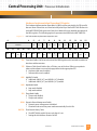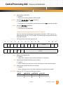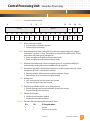
1
User’s Manual
from Emerson Network Power ™
Embedded Computing
PmPPC7448: PowerPC™-Based Processor PMC Module
September 2007
The information in this manual has been checked and is believed to be accurate and reliable. HOWEVER, NO RESPONSIBILITY IS ASSUMED BY EMERSON NETWORK POWER,
EMBEDDED COMPUTING FOR ITS USE OR FOR ANY INACCURACIES. Specifications are subject to change without notice. EMERSON DOES NOT ASSUME ANY LIABILITY ARISING OUT
OF USE OR OTHER APPLICATION OF ANY PRODUCT, CIRCUIT, OR PROGRAM DESCRIBED
HEREIN. This document does not convey any license under Emerson patents or the rights of
others.
Emerson. Consider It Solved is a trademark, and Business-Critical Continuity, Emerson Network Power, and the Emerson Network Power logo are trademarks and service marks of
Emerson Electric Co. © 2007 Emerson Electric Co.
Revision Level:
Principal Changes:
Date:
10006757-00
Original release
October 2005
10006757-01
Artwork stitch, added “RoHS Compliance”,
updated memory map and monitor (version
1.4), added “Internal SRAM”
June 2006
10006757-02
Added caution for front panel reset switch;
updated “Monitor” chapter and environment
variables
September 2007
Copyright © 2005-2007 Emerson Electric Co. All rights reserved.
Regulatory Agency Warnings & Notices
The Emerson PmPPC7448 meets the requirements set forth by the Federal Communications Commission (FCC) in Title 47 of the Code of Federal Regulations. The following information is provided as required by this agency.
This device complies with part 15 of the FCC Rules. Operation is subject to the following two
conditions: (1) This device may not cause harmful interference, and (2) this device must
accept any interference received, including interference that may cause undesired operation.
FCC RULES AND REGULATIONS — PART 15
This equipment has been tested and found to comply with the limits for a Class B digital
device, pursuant to part 15 of the FCC Rules. These limits are designed to provide reasonable protection against harmful interference in a residential installation. This equipment
generates, uses and can radiate radio frequency energy and, if not installed and used in
accordance with the instructions, may cause harmful interference to radio communications. However, there is no guarantee that interference will not occur in a particular installation. If this equipment does cause harmful interference to radio or television reception,
which can be determined by turning the equipment off and on, the user is encouraged to
try to correct the interference by one or more of the following measures:
• Reorient or relocate the receiving antenna
• Increase the separation between the equipment and receiver
• Connect the equipment into an outlet on a circuit different from that to which the
receiver is connected
• Consult the dealer or an experienced radio/TV technician for help
Caution: Making changes or modifications to the PmPPC7448 hardware without the explicit consent
of Emerson Network Power could invalidate the user’s authority to operate this equipment.
!
EMC COMPLIANCE
The electromagnetic compatibility (EMC) tests used a PmPPC7448 model that includes a
front panel assembly from Emerson Network Power.
Caution: For applications where the PmPPC7448 is provided without a front panel, or where the
front panel has been removed, your system chassis/enclosure must provide the required
!
electromagnetic interference (EMI) shielding to maintain EMC compliance.
10006757-02
PmPPC7448 User’s Manual
i
Regulatory Agency Warnings & Notices
(continued)
EC Declaration of Conformity
According to EN 45014:1998
Manufacturer’s Name:
Emerson Network Power
Embedded Computing
Manufacturer’s Address:
8310 Excelsior Drive
Madison, Wisconsin 53717
Declares that the following product, in accordance with the requirements of 2004/108/EEC, EMC
Directive and 1999/5/EC, RTTE Directive and their amending directives,
Product:
PowerPC™-Based Processor PMC Module
Model Name/Number:
PmPPC7448/10005277-xx
has been designed and manufactured to the following specifications:
EN55022:1998 Information Technology Equipment, Radio disturbance characteristics, Limits and
methods of measurement
EN55024:1998 Information Technology Equipment, Immunity characteristics, Limits and methods
of measurement
EN300386 V.1.3.1 Electromagnetic compatibility and radio spectrum matters (ERM);
Telecommunication network equipment; EMC requirements
As manufacturer we hereby declare that the product named above has been designed to comply
with the relevant sections of the above referenced specifications. This product complies with the
essential health and safety requirements of the EMC Directive and RTTE Directive. We have an internal production control system that ensures compliance between the manufactured products and
the technical documentation.
Bill Fleury
Compliance Engineer
Issue date: September 26, 2007
ii
PmPPC7448 User’s Manual
10006757-02
Contents
1 Overview
Components and Features . . . . . . . . . . . 1-1
Functional Overview . . . . . . . . . . . . . . . . 1-3
Physical Memory Map . . . . . . . . . . . . . . . 1-4
Additional Information . . . . . . . . . . . . . . 1-6
Product Certification . . . . . . . . . . . . . 1-6
UL Certification. . . . . . . . . . . . . . . . . . 1-7
RoHS Compliance. . . . . . . . . . . . . . . . 1-8
Terminology and Notation . . . . . . . . 1-8
Technical References. . . . . . . . . . . . . 1-8
2 Setup
Electrostatic Discharge . . . . . . . . . . . . . . 2-1
PmPPC7448 Circuit Board. . . . . . . . . . . . 2-1
Connectors . . . . . . . . . . . . . . . . . . . . . 2-4
LEDs . . . . . . . . . . . . . . . . . . . . . . . . . . . 2-5
Front Panel . . . . . . . . . . . . . . . . . . . . . 2-6
Reset. . . . . . . . . . . . . . . . . . . . . . . . . . . 2-7
PmPPC7448 Setup . . . . . . . . . . . . . . . . . . 2-8
Power Requirements . . . . . . . . . . . . . 2-9
Environmental Considerations . . . . 2-9
Installing the Module. . . . . . . . . . . .2-10
Troubleshooting . . . . . . . . . . . . . . . . . . . 2-11
Technical Support . . . . . . . . . . . . . .2-12
Product Repair . . . . . . . . . . . . . . . . .2-13
3 Central Processing Unit
Processor Reset. . . . . . . . . . . . . . . . . . . . . 3-2
Processor Initialization. . . . . . . . . . . . . . . 3-2
Hardware Implementation Dependent
0 Register. . . . . . . . . . . . . . . . . . . . . . . 3-3
Hardware Implementation Dependent
1 Register. . . . . . . . . . . . . . . . . . . . . . . 3-5
Exception Handling . . . . . . . . . . . . . . . . . 3-6
Exception Processing . . . . . . . . . . . . . . . . 3-8
Machine State Register . . . . . . . . . . . 3-8
Cache Memory . . . . . . . . . . . . . . . . . . . . 3-10
L1 Cache. . . . . . . . . . . . . . . . . . . . . . .3-10
L2 Cache. . . . . . . . . . . . . . . . . . . . . . .3-11
4 On-Card Memory
Configuration
Boot Memory Configuration. . . . . . . . . . 4-1
User Flash . . . . . . . . . . . . . . . . . . . . . . . . . . 4-1
10006757-02
On-Card SDRAM . . . . . . . . . . . . . . . . . . . . .4-2
NVRAM Allocation . . . . . . . . . . . . . . . . . . .4-2
5 System Controller
CPU Interface . . . . . . . . . . . . . . . . . . . . . . .5-2
CPU Interface Registers . . . . . . . . . . 5-2
Memory Interface. . . . . . . . . . . . . . . . . . . .5-2
DDR SDRAM Controller . . . . . . . . . . 5-2
Internal SRAM. . . . . . . . . . . . . . . . . . . 5-3
Device Controller Interface. . . . . . . . . . . .5-3
Device Control Registers . . . . . . . . . 5-4
Internal (IDMA) Controller . . . . . . . . . . . .5-4
Timer/Counter . . . . . . . . . . . . . . . . . . 5-4
PCI Interface . . . . . . . . . . . . . . . . . . . . . . . .5-4
PCI Configuration Space. . . . . . . . . . 5-5
PCI Subsystem Device and Vendor ID
Assignment. . . . . . . . . . . . . . . . . . . . . 5-5
PCI Read/Write. . . . . . . . . . . . . . . . . . 5-5
PCI Interface Registers . . . . . . . . . . . 5-7
PCI Bus Control Signals . . . . . . . . . . . . . . .5-7
PMC Connector Pinouts . . . . . . . . . . . . 5-10
P11 and P12 Pin Assignments . . . . 5-10
P13 and P14 Pin Assignments . . . . 5-11
PMC Connector . . . . . . . . . . . . . . . . 5-12
Doorbell Registers . . . . . . . . . . . . . . . . . 5-13
Outbound Doorbells . . . . . . . . . . . . 5-13
Inbound Doorbells. . . . . . . . . . . . . . 5-13
Monarch Functionality . . . . . . . . . . . . . 5-13
66 MHz Bus Operation. . . . . . . . . . . . . . 5-14
Watchdog Timer . . . . . . . . . . . . . . . . . . 5-14
Reset. . . . . . . . . . . . . . . . . . . . . . . . . . . . . 5-14
6 Ethernet Interface
MV64460 Ethernet Registers . . . . . . . . . .6-1
Ethernet Address . . . . . . . . . . . . . . . . . . . .6-2
Ethernet Connection (P1) . . . . . . . . . . . . .6-2
7 CPLD
Reset Registers . . . . . . . . . . . . . . . . . . . . . .7-1
Reset Event Register (RER). . . . . . . . 7-1
Reset Command Register (RCR) . . . 7-1
PCI Reset Out Enable Register (ROER) .
7-2
Interrupt Registers . . . . . . . . . . . . . . . . . . .7-3
Interrupt Enable Register (IER) . . . . 7-4
PmPPC7448 User’s Manual
iii
Contents
(continued)
Interrupt Pending Register (IPR) . . . 7-4
Product ID Register (PIR). . . . . . . . . . . . . .7-5
EReady Register (ERdy) . . . . . . . . . . . . . . .7-5
Revision Registers . . . . . . . . . . . . . . . . . . .7-5
Hardware Version Register (HVR) . . 7-6
PLD Version Register (PVR) . . . . . . . 7-6
Board Configuration Registers . . . . . . . . .7-6
8 Serial Input/Output
Multi-Protocol Serial Controllers (MPSC)8-1
Serial DMA (SDMA) Channels . . . . . . . . . .8-1
Programmable Baud Rate. . . . . . . . . . . . .8-1
BRGx Configuration Register . . . . . . 8-1
BRGx Tuning Register . . . . . . . . . . . . 8-2
I2C Interface . . . . . . . . . . . . . . . . . . . . . . . .8-2
I/O Connection . . . . . . . . . . . . . . . . . . . . . .8-2
9 Real-Time Clock
Block Diagram. . . . . . . . . . . . . . . . . . . . . . .9-1
Operation. . . . . . . . . . . . . . . . . . . . . . . . . . .9-1
Clock Operation . . . . . . . . . . . . . . . . . . . . .9-2
10 Development Mezzanine
Card
DMC Circuit Board . . . . . . . . . . . . . . . . . 10-1
Serial Numbers . . . . . . . . . . . . . . . . .10-2
Connectors . . . . . . . . . . . . . . . . . . . . . . . 10-3
P1 Connector Pin Assignments . . .10-3
P2 EIA-232 Interface . . . . . . . . . . . .10-6
PmPPC7448 to DMC JTAG . . . . . . . . . . 10-7
P3 JTAG/COP . . . . . . . . . . . . . . . . . . .10-7
P4 JTAG Chain Header . . . . . . . . . . .10-8
DMC Jumpers (JP1). . . . . . . . . . . . . . . . . 10-9
Jumper Setting Register . . . . . . . .10-10
Debug/Status LEDs . . . . . . . . . . . . . . . 10-10
DMC Setup. . . . . . . . . . . . . . . . . . . . . . . 10-11
Installing the DMC Card . . . . . . . .10-11
Troubleshooting . . . . . . . . . . . . . . . . . . 10-13
Technical Support . . . . . . . . . . . . .10-13
Product Repair . . . . . . . . . . . . . . . .10-13
11 Monitor
Command-Line Features. . . . . . . . . . . . 11-1
Basic Operation. . . . . . . . . . . . . . . . . . . . 11-2
iv
PmPPC7448 User’s Manual
10006757-02
Power-up/Reset Sequence . . . . . . 11-2
POST Diagnostic Results . . . . . . . . 11-4
Monitor SDRAM Usage . . . . . . . . . . 11-4
Monitor Recovery and Updates . . . . . . 11-4
Recovering the Monitor . . . . . . . . . 11-4
Updating the Monitor via TFTP . . . 11-5
Restoring the PmPPC7448 Monitor
Using the KatanaQP . . . . . . . . . . . . 11-6
Resetting Environment Variables . 11-7
Accessing the Console Over Ethernet. 11-8
Monitor Command Reference . . . . . . . 11-8
Command Syntax . . . . . . . . . . . . . . 11-9
Command Help . . . . . . . . . . . . . . . . 11-9
Typographic Conventions . . . . . . . 11-9
Boot Commands . . . . . . . . . . . . . . . . . . 11-9
bootd . . . . . . . . . . . . . . . . . . . . . . . . . 11-9
bootelf . . . . . . . . . . . . . . . . . . . . . . . 11-10
bootm . . . . . . . . . . . . . . . . . . . . . . . 11-10
bootp . . . . . . . . . . . . . . . . . . . . . . . . 11-10
bootv . . . . . . . . . . . . . . . . . . . . . . . . 11-10
bootvx . . . . . . . . . . . . . . . . . . . . . . . 11-10
dhcp . . . . . . . . . . . . . . . . . . . . . . . . . 11-11
rarpboot . . . . . . . . . . . . . . . . . . . . . 11-11
tftpboot. . . . . . . . . . . . . . . . . . . . . . 11-11
Memory Commands . . . . . . . . . . . . . . 11-11
cmp . . . . . . . . . . . . . . . . . . . . . . . . . 11-11
cp . . . . . . . . . . . . . . . . . . . . . . . . . . . 11-12
find . . . . . . . . . . . . . . . . . . . . . . . . . . 11-12
md . . . . . . . . . . . . . . . . . . . . . . . . . . 11-12
mm. . . . . . . . . . . . . . . . . . . . . . . . . . 11-13
nm . . . . . . . . . . . . . . . . . . . . . . . . . . 11-13
mw . . . . . . . . . . . . . . . . . . . . . . . . . . 11-13
Flash Commands . . . . . . . . . . . . . . . . . 11-14
cp . . . . . . . . . . . . . . . . . . . . . . . . . . . 11-14
erase . . . . . . . . . . . . . . . . . . . . . . . . 11-14
flinfo. . . . . . . . . . . . . . . . . . . . . . . . . 11-14
protect. . . . . . . . . . . . . . . . . . . . . . . 11-15
EEPROM/I2C Commands . . . . . . . . . . 11-15
eeprom . . . . . . . . . . . . . . . . . . . . . . 11-15
icrc32 . . . . . . . . . . . . . . . . . . . . . . . . 11-16
iloop . . . . . . . . . . . . . . . . . . . . . . . . . 11-16
imd . . . . . . . . . . . . . . . . . . . . . . . . . . 11-16
imm . . . . . . . . . . . . . . . . . . . . . . . . . 11-16
imw . . . . . . . . . . . . . . . . . . . . . . . . . 11-16
inm . . . . . . . . . . . . . . . . . . . . . . . . . . 11-16
iprobe . . . . . . . . . . . . . . . . . . . . . . . 11-16
Environment Parameter Commands 11-17
printenv. . . . . . . . . . . . . . . . . . . . . . 11-17
Contents
(continued)
saveenv . . . . . . . . . . . . . . . . . . . . . .11-17
setenv. . . . . . . . . . . . . . . . . . . . . . . .11-17
Test Commands . . . . . . . . . . . . . . . . . . 11-17
diags . . . . . . . . . . . . . . . . . . . . . . . . .11-18
mtest . . . . . . . . . . . . . . . . . . . . . . . .11-18
um. . . . . . . . . . . . . . . . . . . . . . . . . . .11-18
Other Commands. . . . . . . . . . . . . . . . . 11-18
autoscr . . . . . . . . . . . . . . . . . . . . . . .11-18
base . . . . . . . . . . . . . . . . . . . . . . . . .11-18
bdinfo. . . . . . . . . . . . . . . . . . . . . . . .11-18
coninfo . . . . . . . . . . . . . . . . . . . . . . .11-18
crc32. . . . . . . . . . . . . . . . . . . . . . . . .11-19
date. . . . . . . . . . . . . . . . . . . . . . . . . .11-19
echo . . . . . . . . . . . . . . . . . . . . . . . . .11-19
enumpci. . . . . . . . . . . . . . . . . . . . . .11-19
getmonver. . . . . . . . . . . . . . . . . . . .11-19
go . . . . . . . . . . . . . . . . . . . . . . . . . . .11-19
help. . . . . . . . . . . . . . . . . . . . . . . . . .11-20
iminfo . . . . . . . . . . . . . . . . . . . . . . . .11-20
isdram . . . . . . . . . . . . . . . . . . . . . . .11-20
10006757-02
loop . . . . . . . . . . . . . . . . . . . . . . . . . 11-20
memmap . . . . . . . . . . . . . . . . . . . . 11-20
moninit . . . . . . . . . . . . . . . . . . . . . . 11-20
pci. . . . . . . . . . . . . . . . . . . . . . . . . . . 11-21
ping . . . . . . . . . . . . . . . . . . . . . . . . . 11-21
reset . . . . . . . . . . . . . . . . . . . . . . . . . 11-21
run . . . . . . . . . . . . . . . . . . . . . . . . . . 11-21
script . . . . . . . . . . . . . . . . . . . . . . . . 11-22
showmac. . . . . . . . . . . . . . . . . . . . . 11-22
showpci . . . . . . . . . . . . . . . . . . . . . . 11-22
sleep. . . . . . . . . . . . . . . . . . . . . . . . . 11-22
version . . . . . . . . . . . . . . . . . . . . . . . 11-22
Environment Variables . . . . . . . . . . . . 11-22
Troubleshooting. . . . . . . . . . . . . . . . . . 11-25
Download Formats. . . . . . . . . . . . . . . . 11-25
Binary. . . . . . . . . . . . . . . . . . . . . . . . 11-25
Motorola S-Record . . . . . . . . . . . . 11-25
12 Acronyms
PmPPC7448 User’s Manual
v
(blank page)
vi
PmPPC7448 User’s Manual
10006757-02
Figures
Figure 1-1:
General System Block Diagram. . . . . . . . . . . . . . . . . . . . . . . . . . . . . . . . . . . . . . . . . . . . . . 1-3
Figure 1-2:
PmPPC7448 Memory Map. . . . . . . . . . . . . . . . . . . . . . . . . . . . . . . . . . . . . . . . . . . . . . . . . . 1-4
Figure 2-1:
Component Map, Top (Rev. 06) . . . . . . . . . . . . . . . . . . . . . . . . . . . . . . . . . . . . . . . . . . . . . 2-2
Figure 2-2:
Component Map, Bottom (Rev. 06). . . . . . . . . . . . . . . . . . . . . . . . . . . . . . . . . . . . . . . . . . 2-3
Figure 2-3:
LED Locations, Bottom . . . . . . . . . . . . . . . . . . . . . . . . . . . . . . . . . . . . . . . . . . . . . . . . . . . . . 2-5
Figure 2-4:
Front Panel . . . . . . . . . . . . . . . . . . . . . . . . . . . . . . . . . . . . . . . . . . . . . . . . . . . . . . . . . . . . . . . 2-6
Figure 2-5:
Reset Diagram . . . . . . . . . . . . . . . . . . . . . . . . . . . . . . . . . . . . . . . . . . . . . . . . . . . . . . . . . . . . 2-8
Figure 2-6:
Module Location on Emerson CC1000-DM. . . . . . . . . . . . . . . . . . . . . . . . . . . . . . . . . . . 2-10
Figure 2-7:
Installing the Module . . . . . . . . . . . . . . . . . . . . . . . . . . . . . . . . . . . . . . . . . . . . . . . . . . . . . 2-11
Figure 2-8:
Serial Number and Product ID on Bottom Side . . . . . . . . . . . . . . . . . . . . . . . . . . . . . . . 2-13
Figure 3-1:
MPC7448 Block Diagram . . . . . . . . . . . . . . . . . . . . . . . . . . . . . . . . . . . . . . . . . . . . . . . . . . . 3-2
Figure 5-1:
MV64460 Block Diagram . . . . . . . . . . . . . . . . . . . . . . . . . . . . . . . . . . . . . . . . . . . . . . . . . . . 5-1
Figure 5-2:
PCI Device and Vendor ID. . . . . . . . . . . . . . . . . . . . . . . . . . . . . . . . . . . . . . . . . . . . . . . . . . . 5-5
Figure 5-3:
Example PCI0 Address Map, Monarch . . . . . . . . . . . . . . . . . . . . . . . . . . . . . . . . . . . . . . . . 5-6
Figure 5-4:
Example PCI0 Address Map, Non-Monarch (Default) . . . . . . . . . . . . . . . . . . . . . . . . . . . 5-6
Figure 5-5:
PCI JTAG Block Diagram . . . . . . . . . . . . . . . . . . . . . . . . . . . . . . . . . . . . . . . . . . . . . . . . . . . 5-10
Figure 5-6:
PMC Connector . . . . . . . . . . . . . . . . . . . . . . . . . . . . . . . . . . . . . . . . . . . . . . . . . . . . . . . . . . 5-12
Figure 6-1:
Front Panel Ethernet Connector (P1). . . . . . . . . . . . . . . . . . . . . . . . . . . . . . . . . . . . . . . . . 6-3
Figure 6-2:
Ethernet Cable Assembly . . . . . . . . . . . . . . . . . . . . . . . . . . . . . . . . . . . . . . . . . . . . . . . . . . . 6-3
Figure 8-1:
Front Panel Serial Port Connector (P2) . . . . . . . . . . . . . . . . . . . . . . . . . . . . . . . . . . . . . . . 8-2
Figure 8-2:
Serial Cable Assembly (Emerson Part Number C0007662-00) . . . . . . . . . . . . . . . . . . . 8-3
Figure 9-1:
M41T00 Real-Time Clock Block Diagram . . . . . . . . . . . . . . . . . . . . . . . . . . . . . . . . . . . . . 9-1
Figure 10-1:
DMC Component Maps, Top and Bottom (Revision 01) . . . . . . . . . . . . . . . . . . . . . . . 10-2
Figure 10-2:
DMC P1 PCB-to-PCB Connector . . . . . . . . . . . . . . . . . . . . . . . . . . . . . . . . . . . . . . . . . . . . 10-3
Figure 10-3:
DMC P2 Mini-USB Connector . . . . . . . . . . . . . . . . . . . . . . . . . . . . . . . . . . . . . . . . . . . . . . 10-6
Figure 10-4:
PmPPC7448 to DMC JTAG Block Diagram . . . . . . . . . . . . . . . . . . . . . . . . . . . . . . . . . . . 10-7
Figure 10-5:
DMC P3 JTAG/COP Header. . . . . . . . . . . . . . . . . . . . . . . . . . . . . . . . . . . . . . . . . . . . . . . . . 10-7
Figure 10-6:
DMC P4 JTAG Chain Header. . . . . . . . . . . . . . . . . . . . . . . . . . . . . . . . . . . . . . . . . . . . . . . . 10-8
Figure 10-7:
DMC JP1 Pin Assignments . . . . . . . . . . . . . . . . . . . . . . . . . . . . . . . . . . . . . . . . . . . . . . . . . 10-9
Figure 10-8:
DMC Location on PmPPC7448 . . . . . . . . . . . . . . . . . . . . . . . . . . . . . . . . . . . . . . . . . . . . 10-12
Figure 11-1:
Example Monitor Start-up Display . . . . . . . . . . . . . . . . . . . . . . . . . . . . . . . . . . . . . . . . . . 11-2
Figure 11-2:
Power-up/Reset Sequence Flowchart . . . . . . . . . . . . . . . . . . . . . . . . . . . . . . . . . . . . . . . 11-3
10006757-02
PmPPC7448 User’s Manual
vii
(blank page)
viii
PmPPC7448 User’s Manual
10006757-02
Tables
Table 1-1:
Address Summary . . . . . . . . . . . . . . . . . . . . . . . . . . . . . . . . . . . . . . . . . . . . . . . . . . . . . . . . . 1-5
Table 1-2:
Regulatory Agency Compliance . . . . . . . . . . . . . . . . . . . . . . . . . . . . . . . . . . . . . . . . . . . . . 1-6
Table 1-3:
Technical References . . . . . . . . . . . . . . . . . . . . . . . . . . . . . . . . . . . . . . . . . . . . . . . . . . . . . . 1-8
Table 2-1:
Circuit Board Dimensions . . . . . . . . . . . . . . . . . . . . . . . . . . . . . . . . . . . . . . . . . . . . . . . . . . 2-1
Table 2-2:
Power Requirements . . . . . . . . . . . . . . . . . . . . . . . . . . . . . . . . . . . . . . . . . . . . . . . . . . . . . . 2-9
Table 2-3:
Environmental Requirements . . . . . . . . . . . . . . . . . . . . . . . . . . . . . . . . . . . . . . . . . . . . . . . 2-9
Table 3-1:
PmPPC7448 CPU Features . . . . . . . . . . . . . . . . . . . . . . . . . . . . . . . . . . . . . . . . . . . . . . . . . . 3-1
Table 3-2:
CPU Internal Register Initialization. . . . . . . . . . . . . . . . . . . . . . . . . . . . . . . . . . . . . . . . . . . 3-2
Table 3-3:
MPC7448 Exception Priorities . . . . . . . . . . . . . . . . . . . . . . . . . . . . . . . . . . . . . . . . . . . . . . . 3-7
Table 4-1:
Memory Configuration Jumper. . . . . . . . . . . . . . . . . . . . . . . . . . . . . . . . . . . . . . . . . . . . . . 4-1
Table 4-2:
Flash Memory Configurations . . . . . . . . . . . . . . . . . . . . . . . . . . . . . . . . . . . . . . . . . . . . . . . 4-1
Table 4-3:
NVRAM Memory Map . . . . . . . . . . . . . . . . . . . . . . . . . . . . . . . . . . . . . . . . . . . . . . . . . . . . . . 4-3
Table 5-1:
P11/P12 Pin Assignments—32-Bit PCI . . . . . . . . . . . . . . . . . . . . . . . . . . . . . . . . . . . . . . . 5-10
Table 5-2:
P13/P14 Pin Assignments—64-Bit PCI . . . . . . . . . . . . . . . . . . . . . . . . . . . . . . . . . . . . . . . 5-11
Table 6-1:
Ethernet Port Address Numbering . . . . . . . . . . . . . . . . . . . . . . . . . . . . . . . . . . . . . . . . . . . 6-2
Table 6-2:
Front Panel Ethernet Pin Assignments (P1) . . . . . . . . . . . . . . . . . . . . . . . . . . . . . . . . . . . 6-3
Table 6-3:
Ethernet Cable Wiring Assignments . . . . . . . . . . . . . . . . . . . . . . . . . . . . . . . . . . . . . . . . . 6-3
Table 8-1:
I2C Device Addresses . . . . . . . . . . . . . . . . . . . . . . . . . . . . . . . . . . . . . . . . . . . . . . . . . . . . . . 8-2
Table 8-2:
Front Panel Serial Port Pin Assignments (P2) . . . . . . . . . . . . . . . . . . . . . . . . . . . . . . . . . . 8-3
Table 8-3:
Serial Cable Wiring Assignments . . . . . . . . . . . . . . . . . . . . . . . . . . . . . . . . . . . . . . . . . . . . 8-3
Table 9-1:
RTC Register Map . . . . . . . . . . . . . . . . . . . . . . . . . . . . . . . . . . . . . . . . . . . . . . . . . . . . . . . . . 9-2
Table 10-1:
DMC Mechanical Specifications . . . . . . . . . . . . . . . . . . . . . . . . . . . . . . . . . . . . . . . . . . . . 10-1
Table 10-2:
DMC P1 Connector Pin Assignments . . . . . . . . . . . . . . . . . . . . . . . . . . . . . . . . . . . . . . . . 10-3
Table 10-3:
DMC P2 Pin Assignments . . . . . . . . . . . . . . . . . . . . . . . . . . . . . . . . . . . . . . . . . . . . . . . . . . 10-6
Table 10-4:
DMC P3 Pin Assignments . . . . . . . . . . . . . . . . . . . . . . . . . . . . . . . . . . . . . . . . . . . . . . . . . . 10-8
Table 10-5:
DMC P4 Pin Assignments . . . . . . . . . . . . . . . . . . . . . . . . . . . . . . . . . . . . . . . . . . . . . . . . . . 10-9
Table 11-1:
POST Diagnostic Results . . . . . . . . . . . . . . . . . . . . . . . . . . . . . . . . . . . . . . . . . . . . . . . . . . 11-4
Table 11-2:
Standard Environment Variables . . . . . . . . . . . . . . . . . . . . . . . . . . . . . . . . . . . . . . . . . . 11-22
Table 11-3:
Optional Environment Variables. . . . . . . . . . . . . . . . . . . . . . . . . . . . . . . . . . . . . . . . . . . 11-24
10006757-02
PmPPC7448 User’s Manual
ix
(blank page)
x
PmPPC7448 User’s Manual
10006757-02
Registers
Register 3-1:
MPC7448 Hardware Implementation Dependent, HID0 . . . . . . . . . . . . . . . . . . . . . . . . 3-3
Register 3-2:
MPC7448 Hardware Implementation Dependent, HID1 . . . . . . . . . . . . . . . . . . . . . . . . 3-5
Register 3-3:
CPU Machine State Register (MSR) . . . . . . . . . . . . . . . . . . . . . . . . . . . . . . . . . . . . . . . . . . 3-9
Register 3-4:
L2 Cache Control Register (L2CR). . . . . . . . . . . . . . . . . . . . . . . . . . . . . . . . . . . . . . . . . . . 3-11
Register 7-1:
Reset Event Register (RER) at 0xf820,0000 . . . . . . . . . . . . . . . . . . . . . . . . . . . . . . . . . . . 7-1
Register 7-2:
Reset Command Register (RCR) at 0xf820,1000. . . . . . . . . . . . . . . . . . . . . . . . . . . . . . . 7-2
Register 7-3:
Reset Out Enable Register (ROER) at 0xf820,e000 . . . . . . . . . . . . . . . . . . . . . . . . . . . . . 7-2
Register 7-4:
PmPPC7448 Interrupt Enable Register (IER) at 0xf820,2000 . . . . . . . . . . . . . . . . . . . . 7-4
Register 7-5:
PmPPC7448 Interrupt Pending Register (IPR) at 0xf820,3000 . . . . . . . . . . . . . . . . . . . 7-4
Register 7-6:
PmPPC7448 Product ID Register (PIR) at 0xf820,4000 . . . . . . . . . . . . . . . . . . . . . . . . . 7-5
Register 7-7:
PmPPC7448 ERdy Register (ERdy) at 0xf820,5000 . . . . . . . . . . . . . . . . . . . . . . . . . . . . . 7-5
Register 7-8:
Hardware Version Register (HVR) at 0xf820,7000 . . . . . . . . . . . . . . . . . . . . . . . . . . . . . 7-6
Register 7-9:
PLD Version Register (PVR) at 0xf820,8000 . . . . . . . . . . . . . . . . . . . . . . . . . . . . . . . . . . . 7-6
Register 7-10: PmPPC7448 Board Configuration 3 (BCR3) at 0xf820,c000 . . . . . . . . . . . . . . . . . . . . . 7-6
Register 7-11: PmPPC7448 Board Configuration 1 (BCR1) at 0xf820,a000 . . . . . . . . . . . . . . . . . . . . . 7-7
Register 7-12: PmPPC7448 Board Configuration 0 (BCR0) at 0xf820,9000 . . . . . . . . . . . . . . . . . . . . . 7-7
Register 10-1: DMC Jumper Setting Register at 0xf820,6000. . . . . . . . . . . . . . . . . . . . . . . . . . . . . . . 10-10
Register 10-2: DMC LED Register at 0xf820,d000 . . . . . . . . . . . . . . . . . . . . . . . . . . . . . . . . . . . . . . . . . 10-10
10006757-02
PmPPC7448 User’s Manual
xi
(blank page)
xii
PmPPC7448 User’s Manual
10006757-02
Section 1
Overview
The Emerson PmPPC7448 module is a Processor PCI Mezzanine Card (PPMC). It is based on
the Freescale® Semiconductor PowerPC™ MPC7448 central processor unit and provides
additional processing power for the baseboard, which must be compatible with PPMC
architecture. The PmPPC7448 module supports various memory configurations, programmable user Flash memory, a PCI bridge/controller, three Ethernet interfaces, two serial
ports, as well as a real-time clock, and EEPROM.
COMPONENTS AND FEATURES
The following is a brief summary of the PmPPC7448 hardware components and features:
CPU: The Freescale MPC7448 RISC PowerPC microprocessor has an internal speed of up to 1.4
GHz and 166 MHz local bus speed. The MPC7448 includes 32 kilobytes separate level-one
(L1) data and instruction caches and 1 megabyte L2 cache. Standard power supply is 3.3
volts, with a configuration option for both 3.3 and 5 volts.
System Controller/PCI Bridge:
The Marvell® MV64460 (Discovery™III) is a single-chip solution that provides one PCI-X
bus, three integrated gigabit Ethernet Medium Access Control (MAC) controllers, twomegabit integrated Synchronous Random Access Memory (SRAM), four Independent
Direct Memory Access (IDMA) engines and two XOR Direct Memory Access (DMA) engines.
The 64-bit PCI interface can operate up to 66 MHz (60X) or 133 MHz (PCI-X).
SDRAM: The PmPPC7448 includes a 32M x 72-bit Double Data Rate (DDR) Synchronous Dynamic
Random Access Memory (SDRAM) Small-Outline Dual In-line Memory Module (SO-DIMM).
Options include 256 megabytes, 512 megabytes, 1 gigabyte, and 2 gigabytes. The interface implements eight additional bits to permit the use of error-correcting code (ECC). The
MV64460 bridge acts as the memory controller.
Flash: The PmPPC7448 includes Flash configuration options of 32 or 64 megabytes. The
PmPPC7448 is capable of booting from either an 8-bit, 32-pin PLCC ROM socket on the
Development Mezzanine Card (DMC) or from 32-bit soldered Flash (default).
Serial I/O: The PmPPC7448 includes up to two EIA-232 ports operating between 9600 and 115,200
baud. Serial port one is always routed to the Development Mezzanine Card (DMC) serial
connector; build options include connections to the front panel serial connector, or the P14
connector. When routed to P14, the port has the option of either EIA-232 or TTL signaling
levels. Serial port two is routed to P14 with the same signaling options.
Ethernet: The PmPPC7448 includes three Ethernet ports. Two Broadcom BCM5461S gigabit PHY
devices route Ethernet (ports 0 and 1) through connector P14. The Micrel KSZ8721CL
10/100 PHY device routes Ethernet (port 2) through a mini-USB connector on the front
panel. The Broadcom and Micrel devices are IEEE 802.3-compliant.
10006757-02
PmPPC7448 User’s Manual
1-1
Overview:
Components and Features
Note: GbE ports (0 and 1) are routed through the PHYs directly to connector P14. Therefore, magnetics are
required on the Rear Transition Module (RTM) or baseboard.
CPLD: The PmPPC7448 uses a Complex Programmable Logic Device (CPLD) to implement various
memory-mapped registers and to control access to the Flash, ROM socket, and enumeration of Monarch/non-Monarch systems.
RTC: The real-time clock is an ST®Microelectronics M41T00 Serial Access Timekeeper®.
Development Mezzanine Card (DMC):
The DMC is a custom, optional plug-on card mounted on the back of the PmPPC7448. This
card facilitates hardware and software development. See Chapter 10.
1-2
PmPPC7448 User’s Manual
10006757-02
Overview:
Functional Overview
FUNCTIONAL OVERVIEW
The following block diagram provides a functional overview for the PmPPC7448:
Figure 1-1: General System Block Diagram
Mini-USB
P1
Front Panel
Mini-USB
P2
DMC Connector
MPX Bus
up to 166 MHz
Flash
32/64 MB
Port 2
(portdbg)
10/100
PHY
MII
Device Bus
Mini USB
Connector
10/100
Magnetics
COP Debug
Development
Mezzanine Card
(DMC)
Motorola
MPC7448
Microprocessor
512 K
Socketed
Flash
Jumpers
Marvell
MV64460
System
Controller
MPP Bits
LEDs (4)
Device
CPLD
PLD JTAG
Serial1
EIA-232
Tranceivers
Serial2
Port 1
(portb)
GMII
Port 0
(porta)
GMII
I2C
GbE
PHY
GbE
PHY
Marvell
Config.
SEEPROM
NVRAM
SEEPROM
8 KB
ST Micro
M41T00
RTC
SROM
PCI 0
DRAM Bus
133 MHz
PCI/PCI-X 64-bit PMC
(3.3 V only)
P11
P12
DDR SDRAM
256 MB, 512 MB,
1 GB, 2 GB
GPIO
1.1 V
Supply
1.25 V
Supply
1.5 V
Supply
1.8 V
Supply
2.5 V
Supply
3.3 V
Supply
P13
P14
10006757-02
PmPPC7448 User’s Manual
1-3
Overview:
Physical Memory Map
PHYSICAL MEMORY MAP
Fig. 1-1 illustrates the PmPPC7448 memory map:
Figure 1-2: PmPPC7448 Memory Map
Hex Address
FFFF,FFFF
Hex Address
Boot Mirror
FF80,0000
Reserved
F854,0000
F850,0000
F830,0000
F820,0000
F810,0000
F800,0000
F820,E000
F820,D000
F820,C000
F820,B000
F820,A000
F820,9000
F820,8000
F820,7000
F820,6000
F820,5000
F820,4000
F820,3000
MV64460 SRAM
Reserved
CPLD
MV64460
ROM Socket
Reserved
EBFF,FFFF
E9FF,FFFF
E800,0000
Flash
64 MB
Flash
32 MB
Reserved
C000,0000
I/O
B000,0000
8000,0000
3FFF,FFFF
1FFF,FFFF
0FFF,FFFF
PCI 0
Memory
SDRAM
SDRAM 512 MB
0000,0000 256 MB
1-4
PmPPC7448 User’s Manual
SDRAM
2 GB
Reserved
SDRAM
1 GB
10006757-02
F820,2000
F820,1000
F820,0000
PCI Reset Out Enable Register
DMC LED Register
Board Configuration Register 3
Reserved
Board Configuration Register 1
Board Configuration Register 0
PLD Version Register
Hardware Version Register
Jumper Settings Register
EREADY Register
Product ID Register
Interrupt Pending Register
Interrupt Enable Register
Reset Command Register
Reset Event Register
Overview:
Physical Memory Map
Table 1-1 summarizes the physical addresses for the PmPPC7448 and provides a reference
to more detailed information:
Table 1-1: Address Summary
Hex Physical
Address:
Access
Mode:
Description:
See Page:
FF80,0000
R/W
Boot Mirror
–
–
FF80,0000
R/W
Boot Mirror
F854,0000
–
Reserved
–
MV64460 SRAM
5-3
F850,0000
F830,0000
–
Reserved
–
F820,E000
R/W
PCI Reset Out Enable register
7-2
F820,D000
W
DMC LED register
10-10
F820,C000
R
Board Configuration register 3 (BCR3)
7-6
F820,B000
–
Reserved (BCR2)
–
F820,A000
R/W
Board Configuration register 1 (BCR1)
7-6
F820,9000
R
Board Configuration register 0 (BCR0)
7-6
F820,8000
R
PLD Version register (PVR)
7-6
F820,7000
R
Hardware Version register (HVR)
7-6
F820,6000
R
Jumper Settings register (JSR)
10-10
F820,5000
R/W11
EReady (ERdy) register
7-5
F820,4000
R
Product ID register (PIR)
7-5
F820,3000
R/W
Interrupt Pending register (IPR)
7-4
F820,2000
R/W
Interrupt Enable register (IER)
7-4
F820,1000
W
Reset Command register (RCR)
7-2
F820,0000
R
Reset Event register (RER)
7-1
7-1
F820,0000
R/W
CPLD
F810,0000
R/W
MV64460
5-5
F800,0000
R/W
4-1
EBFF,FFFF
–
ROM Flash Socket
Reserved 2
E800,0000
R/W
Flash (32 MB, 64 MB)
4-1, 11-14
–
C000,0000
–
Reserved
–
8000,0000
R/W
PCI 0 — Memory and I/O Space
5-4
0000,0000
R/W
SDRAM (256 MB, 512 MB, 1 GB, 2 GB)
4-2
1.If Monarch, read only; if non-Monarch, write only.
2.Depends on Flash size.
10006757-02
PmPPC7448 User’s Manual
1-5
Overview:
Additional Information
ADDITIONAL INFORMATION
This section lists the PmPPC7448 hardware regulatory certifications and briefly discusses
the terminology and notation conventions used in this manual. It also lists general technical
references.
Mean time between failures (MTBF) has been calculated at 309,632 hours using Telcordia
Issue 1 Method I Case 3.
Product Certification
The PmPPC7448 hardware has been tested to comply with various safety, immunity, and
emissions requirements as specified by the Federal Communications Commission (FCC),
Industry Canada (IC), Underwriters Laboratories (UL), and the European Union Directives
(CE mark). The following table summarizes this compliance:
Table 1-2: Regulatory Agency Compliance
Type:
Safety
Specification:
UL60950-1, CSA C22.2 No. 60950-1-03, 1st Edition – Safety of
Information Technology Equipment, including Electrical Business
Equipment (Bi-National)
IEC60950/EN60950 – Safety of Information Technology Equipment
(Western Europe)
AS/NZS 60950– Safety Standard for Australia and New Zealand
Environmental
1-6
PmPPC7448 User’s Manual
NEBS: Telcordia GR-63 –
Section 4.1 Transportation and Storage
Section 4.3 Equipment Handling
Section 4.4.3 Office Vibration
Section 4.4.4 Transportation Vibration
Section 4.5 Airborne Contaminants
10006757-02
Overview:
Additional Information
Type:
EMC
Specification:
FCC Part 15, Class B – Title 47, Code of Federal Regulations, Radio
Frequency Devices
ICES 003, Class B – Industry Canada Interference-causing Equipment
Standard for Digital Apparatus, Radiated and Conducted Emissions
NEBS: Telcordia GR-1089 level 3 – Emissions and Immunity (circuit pack
level testing only)
AS/NZS 3548 003, Class A – Standard for radiated and conducted
emissions for Australia and New Zealand
EN55022, Class B – Information Technology Equipment, Radio
Disturbance Characteristics, Limits and Methods of Measurement
EN55024 – Information Technology Equipment, Immunity
Characteristics, Limits and Methods of Measurement
EN300386-2 – Electromagnetic Compatibility and Radio Spectrum
Matters (ERM); Telecommunication Network Equipment;
Electromagnetic Compatibility (EMC) Requirements
VCCI, Class 2 – Radiated and Conducted Emissions (Japan)
Note: EMC testing was performed without the front panel serial or Ethernet cables installed. These ports are for
debug purposes only. Also, EMC testing was not performed for the configuration with the taller heatsink (for
15 mm connector stackup). This configuration is designed for use on a customer’s proprietary carrier that
can support 15 mm PCI mezzanine cards. It is the customer’s responsibility to test this PmPPC7448 configuration in their system.
Emerson maintains test reports that provide specific information regarding the methods
and equipment used in compliance testing. Unshielded external I/O cables, loose screws, or
a poorly grounded chassis may adversely affect the PmPPC7448 hardware’s ability to comply with any of the stated specifications.
UL Certification
The UL web site at ul.com has a list of Emerson’s UL certifications.
1 To find the list, search in the online certifications directory using Emerson’s UL file number,
E190079.
2 There is a list for products distributed in the United States, as well as a list for products
shipped to Canada. To find the PmPPC7448, search in the list for the model name and/or
number. The PmPPC7448 is a Processor PCI Mezzanine Card (PPMC). The model number is
PmPPC7448’s Printed Circuit Board (PCB) artwork number, which is 10005277-xx (xx
changes with each artwork revision).
10006757-02
PmPPC7448 User’s Manual
1-7
Overview:
Additional Information
RoHS Compliance
The PmPPC7448 is compliant with the European Union’s RoHS (Restriction of Use of Hazardous Substances) directive created to limit harm to the environment and human health
by restricting the use of harmful substances in electrical and electronic equipment. Effective July 1, 2006, RoHS restricts the use of six substances: cadmium (Cd), mercury (Hg),
hexavalent chromium (Cr (VI)), polybrominated biphenyls (PBBs), polybrominated diphenyl ethers (PBDEs) and lead (Pb). Configurations that are RoHS compliant are built with
lead-free solder. Configurations that are 5-of-6 are built with tin-lead solder per the lead-insolder RoHS exemption.
To obtain a certificate of conformity (CoC) for the PmPPC7448, send an e-mail to
[email protected] or call 1-800-356-9602. Have the part number(s) (e.g., C000######) for your configuration(s) available when contacting Emerson.
Terminology and Notation
Active low signals: An active low signal is indicated with an asterisk * after the signal name.
Byte, word: Throughout this manual byte refers to 8 bits, word refers to 16 bits, long word refers to 32
bits, and double long word refers to 64 bits.
MAC: This manual uses the acronym MAC to refer to both a medium access control address and
the media-specific access control protocol within IEEE 802 specifications.
PLD: This manual uses the acronym PLD as a generic term for programmable logic device (also
known as FPGA, CPLD, EPLD, etc.).
Radix 2 and 16: Hexadecimal numbers either end with a subscript 16 or begin with 0x. Binary numbers are
shown with a subscript 2.
Technical References
Further information on basic operation and programming of the PmPPC7448 components
can be found in the following documents:
Table 1-3: Technical References
Device / Interface:
Document: 3
CPU
MPC7450 RISC Microprocessor Family User’s Manual
(Freescale Semiconductor MPC7450UM Rev. 4.2 10/2004)
http://www.freescale.com
System controller/
PCI bridge
Discovery™ III PowerPC® System Controller MV64460 Product Brief
(Marvell, MV64460-001 9/03)
http://www.marvell.com
VESA Unified Memory Architecture
http://www.vesa.org
1-8
PmPPC7448 User’s Manual
10006757-02
Overview:
Additional Information
Device / Interface:
Ethernet
Document: 3
(continued)
KSZ8721CL 3.3V Single Power Supply 10/100BASE-TX/FX MII Physical Layer
Transceiver Data Sheet
(Micrel® Inc., Rev. 1.2, M9999-041405 April 2005)
http://www.micrel.com
BCM5461S 10/100/1000BASE-T Gigabit Ethernet Transceiver Data Sheet
(Broadcom® Corporation, 5461S-DS05-R 09/02/04)
http://www.broadcom.com
Flash
Intel ® StrataFlash® Embedded Memory (P30) Datasheet
(Intel, Order Number: 306666 Revision: 002 August 2005)
http://www.intel.com
Real-Time Clock
Serial Access Timekeeper® M41T00
(ST®Microelectronics, July 2001)
http://www.st.com
SDRAM (SO-DIMM)
Module
32M X 72 Bits (256MB) 200-Pin DDR SDRAM SO-DIMM with ECC
(SimpleTech, Inc. Doc. Part Number 61000-01906-101 June 2001)
http://www.simpletech.com
PCI
PCI Local Bus Specification
(PCI Special Interest Group, Revision 2.2, December 18, 1998)
PCI-X Addendum to the PCI Local Bus Specification
(PCI Special Interest Group, Revision 1.0a, July 24, 2000)
http://www.pcisig.com
PMC
IEEE Standard for a Common Mezzanine Card (CMC) Family: IEEE Std 13862001
(IEEE: New York, NY)
IEEE Standard for Physical and Environmental Layers for PCI Mezzanine Cards:
IEEE Std 1386.1-2001
(IEEE: New York, NY)
http://www.ieee.org
PPMC
Processor PMC Standard for Processor PCI Mezzanine Cards: VITA 32-2003
Revision 1.0a / 29 April 2003
(VITA: Scottsdale, AZ)
http://www.vita.com
3.Frequently, the most current information regarding addenda/errata for specific documents may be found on
the corresponding web site.
10006757-02
PmPPC7448 User’s Manual
1-9
(blank page)
1-10
PmPPC7448 User’s Manual
10006757-02
Section 2
Setup
This chapter describes the physical layout of the boards, the setup process, and how to
check for proper operation once the boards have been installed. This chapter also includes
troubleshooting, service, and warranty information.
ELECTROSTATIC DISCHARGE
Before you begin the setup process, please remember that electrostatic discharge (ESD)
can easily damage the components on the PmPPC7448 hardware. Electronic devices, especially those with programmable parts, are susceptible to ESD, which can result in operational failure. Unless you ground yourself properly, static charges can accumulate in your
body and cause ESD damage when you touch the board.
Caution: Use proper static protection and handle PmPPC7448 boards only when absolutely
necessary. Always wear a wriststrap to ground your body before touching a board. Keep
!
your body grounded while handling the board. Hold the board by its edges–do not touch
any components or circuits. When the board is not in an enclosure, store it in a staticshielding bag.
To ground yourself, wear a grounding wriststrap. Simply placing the board on top of a
static-shielding bag does not provide any protection–place it on a grounded dissipative
mat. Do not place the board on metal or other conductive surfaces.
PMPPC7448 CIRCUIT BOARD
The PmPPC7448 is a fourteen-layer circuit board that conforms to the IEEE 1386 Common
Mezzanine Card (CMC) standard. It has the following physical dimensions:
Table 2-1: Circuit Board Dimensions
Width:
2.913 in.
(74 mm)
Depth:
Height (top side):
Height (bottom side):
5.866 in.
(149 mm)
0.323 in. (I/O area, 0.524 in.)
(8.2 mm, I/O area is 13.5 mm)
0.007 in.
(1.9 mm)
10006757-02
PmPPC7448 User’s Manual
2-1
Setup:
PmPPC7448 Circuit Board
The following figures show the component maps for the PmPPC7448 circuit board.
Figure 2-1: Component Map, Top (Rev. 06)
R1
SW1
R5
RN3
R175
R183
C9
C15
C19
R37
R38
R39
R585
R562
R40
R41
C321
RN4
C18
R6
R11
R10
R18
R22
R23
R29
R19
R25
R24
R31
R30
R36
R8
R7
R13
R12
R20
R27
R26
R32
C17
C110
C325
C300
R563
C323
C326
C5
R34
R33
P2
U1
MPC7447
CPU
U2
R564
C320
R4
RN1
RN2
C1
R3
R2
C16
P1
R42
R505
R507
R510
R511
R508
U3
SODIMM
R43
C26
C39
PmPPC7448 User’s Manual
R90
R91
C62
U14 U15
C48
64 2
C54
C58
64 2
C24
C38
C40
L4
C41
C44
L5
C49
R80
R76
C36
C37
63
P13
C56
C60
63 1
P12
C295 C35
P14
R485 R487 R489 R491
R488 R490 R486 R484
10006757-02
64
R482 R483
R470 R472
R471R473
R291
R82
R81
R84
R83
C53
L3
R88
U12
U13
U7
R86
C57
R87
C61
M6
U11
C280
M5
1
C47
C25
U8
63 1
C52
2-2
U10
C281
P11
2
2
C51
R78
R79
C50 U9
C22
C294
C30
RN14 RN15
R51 R53
R52 R54 R55
RN16 R57 R50
R58 R61 R63 R65
R56
RN17 R66 R59 R60 R62
R68
RN18 R67
R71
R70
R73
RN19 R72
R85
C55
R89
C59
1
C286
R492 R493
R64
C45
C63
R293
R504
R69
C42
C43
R75
C46
C29
L2
C33
R48
RN12 RN13
C31
RN9
RN10 RN11
C32
C199
C28
C27
R47
RN7
U4
MV64460
System Controller
R303 R306
R308 R307
C34
RN6
RN8
U5 U6
C23
RN5
C253
63
64
Setup:
PmPPC7448 Circuit Board
R123
R122
CR11
R526
R527
CR10
R132
R131
C191
R351
R350
C195
RN170RN167
R49
R394
Y2
R433
R290
R422
R425
R442
R474
R436
R426
R481 R430
C297 R435
R434
U35
C277 R452
R390
C239
R395
R407
R415
R414 RN178
R419
R502
C278
CR24
R456
10006757-02
R444
U29
R443
R495
R431
C334
R446
C243
RN172
R392
R391
RN174
RN173
R570
R569
R571
R572
R574
R573
R575
R576
R440
R447
U37 U28
R408
R416
R421
R420
C254
C259 R469 R423
R428
C258
R427
C264
C269 R432 R453
C270
U31
GbE
R364
RN169 RN168
R376 R375 RN171
R379
C229 R344
R467 R466
R475
C170
R480
C282
R465 R74
C240
RN159
RN162
R361
C222
C247 C242
C246 C241
C233
R454 C344
C236
R397
CR27
R459
C223
R464
R349
C219
R377
R370
RN175
RN176
R460
R451
R450
CR28
CR29
C143
C146
C303
R318
R317
RN158 RN147 RN138
RN157 RN146
R341
R343
R342
R347
R348
R383 R374
R373 C225
R382 C226 C224
R381 R372
R380 R371
L21
C186
R329 RN141RN140 RN139
C197 C196 R334 R333
C203 C201 R340 R339
C202
C211 RN152
RN150
RN151
C210
C220
R455
R461
R352
RN164 RN160
R457
CR30
L19
C335C336C337C338C276R441
R449 R448
RN120
RN131
R296
R301
R273 RN129
RN130
RN136
RN132
RN124
RN166 RN163
R367 R365
R366
C331
Y3
CR22
RN117
RN79RN118
RN91
RN128
RN125
C333
R445
C332
U36RN188 RN187 C279 C275
RN126
CR25
R267
R268
R463
R321
R320
C184
R336 R326 R315
R330 R325
C230
R385
CR21R384
R439
R438
C268
U32
GbE
RN80
RN92
RN121
C234
CR26
U34 U33
R412
R418
C251
C257
C256
C263
C267
RN122
R254
RN103 RN102
RN135 RN137 RN133
RN143
R255
RN142
RN149 RN148RN145
C208
RN144 C209
RN156 RN155
C214
RN154
RN153C213
RN161
C238
C237
R398
R411 C244
R410 R409
R417 C249
C250 C248
C255
R400 C261
C262 C260
C266 C265
C274 C272
C273 C271
R399
RN81
RN93
R298
R346
R345
R355 R354 R353
R359 R358 R357
R356
R363
R362
R368
R369
R378
L18
RN82
RN94
RN123 RN119 RN115
RN127
RN134
R578
R577
R579
R580
R582
R581
R583
R584
R413
R406
R405
R404
R403
R429 R424 C252 R402
R401
C245
U30
C235
R388
RN177
R389 C231
M4
R393
C232
R387
C228
C227
C285
R477
R476
M2
L13
R360 CR16
R479 U38
M3
L22
R478
RN69
C129
RN67 C142 C144
RN68
RN106 RN105 RN104
C21 C174
R319
RN70
RN95
C307
C311
R501 RN114 RN113
RN116
U26
U27
C215
C284 CR15
R337 C188 C180
C200 C190 R316
R332
R331 C189
R338 R328
R327
C185
Y4
C305 R555
RN97 RN96
C20
C171 R294
R295 R300 R299 C172
R305 C173 R519
M1
RN62
U40
C306
R462
R283
R282
RN108
RN98
RN99
U18
PLD
C136
C135
RN107
C153 R238
R281 R517
R500
R516
C122
C165 C162 C156
R280 R265
C151 C134
R236
R235
R279 R264
C150 C133
R234
R233 R551
R552C128
R232 R550
C221C218
R323
R219R206
R278 R263
C304
C198 L12
C149
L17
R549 C309C121
C179
RN66
C212 R324
R314
R277 R262
C148
C183 C178 R522
RN65
C164 C161
C207 C194
C147
C217
C193C182 C177
C206 C192
R523 C160
C181
C176
RN64
C205
R297
L16
C159
C204
R313
C127
R276 R261
L15
R557 R548
R322 R312
R230
R212 C126
C216
C187 R311
R229
R213
R335 L11 C175
R211 R200
C131
C169 C158
C145 R228
R210 R199
R198
R208
R227
R209 R197
R274
L14
R196
C163 R260
R253
R195
R292 R275 R259
C125
R289
R288
C327
C139
R247
R246
C138
R245
R244
C137
R537
R536
R542
R535
C155
R287 R272
RN111 RN100
R286 R271
R285 R270
C166
RN88
RN110
R284 R269
RN109
R250
C141
C140
RN89
RN52
RN57
R166
RN60
RN75 RN74 RN73 RN72 C152 RN71
R518
RN87 RN86 RN85 RN84
RN83
RN76
CR14
R546
R545
R544
U41
C345
R225 R203
R217
R503
C124
C120
R193
R192
R191
R190
R189
R188
R187
C298
C157
C168
C167 R252 R258
R257
R256
RN112
R543
R223
R218
R249
RN77
R251 RN90
RN101
U24
R179
R185
RN41
C106C105
R134
R140
R139
RN29 R142
R151
RN40 R150
R153
RN51 R157
R161 R156
R160 R159
R165
RN56 R164
R168
RN59 R172
R171
R174
R182
R194
RN28
C130
RN78
R180
R541
C118
C91
R528
R529
R530
R533
C328
RN54
R231
R521
R226
C313
R44
RN61
R45
R309 RN63
R46 R304
R205
R221R310 R204
C343
C317
RN58
U42
RN27 RN26RN25 R137 R136 RN24
C109
RN30
R144
R143
R152
R155
R154
R158
R163
R162
R167
R170
R169
R173
R177
R176
U19
Flash
RN165
RN55
C312
U20
Flash
C154
R561 C315 C116
RN53
R566 R565
R568 R567
R124
R524
C123
RN34 RN33RN32RN31
C119 RN45RN44 RN43RN42
R559
R396
RN46
C107
R202
C302
R538
R539
C301
R547
R146
C308
C111
R222C117 C314C115 C114 C113 R145
R186
R141
R512
C112 RN50 RN49RN48RN47
R149 R138
R148
R147
R509
RN35
RN39 RN38RN37RN36
Y1
P3
PMC-to-PMC
R133
U16
U39
C100
C104
CR23
C103 C102
R128
R127
C76
R118
C75 C74
C84 R119 C82
C85 C83 R121 R120
C94
C92
C93
R125 R129
R468
C98
C99
C101
RN189 R532
R531
C324
C81
R514
C97
R520
C29
C14
C299R506
C78
C77
C87
C86
C95
R99
C319
R534
R115
C80
C79
C90 C88
C89
C96
C72
R513
R111
C64
R100 C66
C68 R103
R102
R104
C71
R114
R110
R109
R108
C322
R107
R525
C310
C73
C318
C67
C69
R117
R116
R113 R106
R112 R105
R515
L9
L8
L7
L6
R494 C70
C108
R98 C65 R97 R96
R101
R458
684-
RN21RN20 R93
R94 R92
1000XXXX-XX D
XXXXXX
CR5
R95
CR4
CR3
CR2
CR1
Figure 2-2: Component Map, Bottom (Rev. 06)
PmPPC7448 User’s Manual
2-3
Setup:
PmPPC7448 Circuit Board
Connectors
The PmPPC7448 has the following connectors:
P1: This mini-USB (universal serial bus) is the connection to the front panel 10/100 PHY Ethernet (port 2). Refer to Table 6-2 for the pin assignments.
P2: P2 is a mini-USB connector for the front panel serial port. Refer to Table 8-2 for the pin
assignments.
P3: This is an 80-pin PCB-to-PCB male connector on the bottom side of the PmPPC7448. P3
routes memory, CPLD, and CPU signals from the PmPPC7448 to the DMC for development
use. See Table 10-2 for the pin assignments.
P11, P12, P13: These 64-pin connectors provide the standard 64-bit PCI interface between the
PmPPC7448 and the PMC host. See Table 5-1 for pinouts.
P14: This 64-pin connector conforms to the PCI specification as user-defined. Ethernet signals
are also available at P14. See Table 5-2 for pinouts.
U3: This is the socket for the small-outline, dual inline memory module (SO-DIMM). The SODIMM board layout depends on the memory configuration and manufacturer.
2-4
PmPPC7448 User’s Manual
10006757-02
Setup:
PmPPC7448 Circuit Board
LEDs
The PmPPC7448 has fifteen green light-emitting diodes (LEDs) on the back side of the
board (see Fig. 2-3).
CR4
CR3
CR2
CR1
CR5
Figure 2-3: LED Locations, Bottom
CR11
P3-DMC
CR10
CR1-Debug LED4
CR2-Debug LED3
CR3-Debug LED2
CR4-Debug LED1
CR5-MPC7448 Check stop out
Port 2 Ethernet
(10/100BASE-TX/FX)
CR10-Link
CR11-Activity
Port 1 Ethernet
Port 0 Ethernet
CR27-Activity
CR28-Link
CR29-Link1
CR30-Link2
CR23-Activity
CR24-Link
CR25-Link1
CR26-Link2
CR23
CR24
CR26
(10/100/1000BASE-T)
CR25
CR27
CR28
CR30
CR29
(10/100/1000BASE-T)
10006757-02
PmPPC7448 User’s Manual
2-5
Setup:
PmPPC7448 Circuit Board
Front Panel
The PmPPC7448 has a single-wide PPMC front panel with an Electromagnetic Interference
(EMI) gasket.
Note: The electromagnetic compatibility (EMC) tests used a PmPPC7448 model that includes a
front panel assembly from Emerson.
Caution: For applications where the PmPPC7448 is provided without a front panel, or where the
front panel has been removed, your system chassis/enclosure must provide the required
!
electromagnetic interference (EMI) shielding to maintain EMC compliance.
Figure 2-4: Front Panel
Ethernet
P1 Ethernet connector
Reset
SW1
P2 serial connector
Serial
2-6
PmPPC7448 User’s Manual
10006757-02
Setup:
PmPPC7448 Circuit Board
Reset
The reset signals are routed to the CPLD, unless stated otherwise. See Chapter 7 for the
reset registers. The following sources can reset the PmPPC7448:
Power-on: This causes a hard reset to the entire board, including the PCI interfaces.
Front panel: This reset switch is accessible through a small hole in the front panel and causes a hard reset
to the entire board, including the PCI interfaces.
Caution: Use minimal force when pressing the front panel reset switch. Excessive force may damage
the switch.
!
PCI RESET: This causes a hard reset to the entire board, including the PCI interfaces.
COP HRESET: This reset is activated by the common on-chip processor (COP) debugger interface via a
header located on the Development Mezzanine Card (DMC). It causes a hard reset to the
entire board, including the PCI interfaces.
COP SRESET: This reset is activated by the COP debugger interface and causes a soft reset to the Freescale MPC7448 and a reset to Flash.
COP TRST: This is routed directly to the MPC7448 TRST.
PMC TRST: This is routed directly to the MV64460 TRST.
Software controlled: The software controlled resets are described in the Reset Command register, Register
Map 7-2.
10006757-02
PmPPC7448 User’s Manual
2-7
Setup:
PmPPC7448 Setup
Figure 2-5: Reset Diagram
DEBUG_HRESET
DEBUG_SRESET
DEBUG_TRST
DMC_PD
P11/P12
Development
Mezzanine
Card
ENET_RST*
DMC_BOOT_SRC
PMC_CPLD_PCI_REQ64*
PMC_CPLD_PCI_DEVSEL*
PMC_CPLD_PCI_STOP*
PMC_CPLD_PCI_TRDY*
Ethernet
RGMII
(port0)
Ethernet
MII
(portdbg)
Ethernet
RGMII
(port1)
MPC7448_HRESET*
MPC7448_SRESET*
MPC7448
MPC7448_TRST*
PMC_CPLD_PCI_RST*
PMC_RESET_OUT*
CPLD
CPLD_MV_64EN*
PER_AD(31:0)*
MV_SYSRST*
MV_INIT_ACT
POR_RST*
MV_WDE
FLASH_RP*
Voltage
Monitor
MV64460
PCI Bridge
PCI_RST*
OSC_EN
Voltage
Monitor
Init ROM
I2C
MV_SCL
MV_SDA
PMC_CPLD_PCI_RST_R*
Flash
PMPPC7448 SETUP
You need the following items to set up and check the operation of the Emerson
PmPPC7448:
❐ An Emerson PmPPC7448 board
❐ A compatible host board, such as the Emerson CC1000-DM or Katana750i
❐ Card cage and power supply
❐ CRT terminal
When you unpack the board, save the antistatic bag and box for future shipping or storage.
2-8
PmPPC7448 User’s Manual
10006757-02
Setup:
PmPPC7448 Setup
Caution: Do not install the board in a rack or remove the board from a rack while power is applied, at
risk of damage to the board.
!
Power Requirements
Be sure your power supply is sufficient for the PmPPC7448 circuit board. Standard power is
3.3 volts, however a dual power supply option is available. Table 2-2 lists the board’s specific
power requirements.
Table 2-2: Power Requirements
Voltage:
Range:
Current
(typical):
+3.3 V
+/- 5%
5.1 amps
Watt Requirements/Configuration:
1 GHz MPC7448 and 1 GB DDR SDRAM
configuration typically requires 17 watts
Specific PmPPC7448 configurations may draw over 20 watts of power. The configurations
with a faster core CPU frequency and increased DDR memory draw more power and generate more heat. When monitoring the ambient air temperature increase across the module
(from the inlet side of the PmPPC7448 to the outlet), the temperature can rise approximately 4-7° C at high airflow (300 lfm) to 5-12° C at low airflow (100 lfm). The system
designer should consider the cumulative effects of installing multiple PMC modules on a
single carrier and ensure adequate airflow.
Environmental Considerations
As with any printed circuit board, be sure that air flow to the board is adequate. Chassis
constraints and other factors greatly affect the air flow rate. The environmental requirements are as follows:
Table 2-3: Environmental Requirements
Environment:
Range:
Relative Humidity:
Operating Temperature
0° to +55° Centigrade, ambient
(at board)
Not to exceed 85%
(non-condensing)
Storage Temperature
—40° to 85° Centigrade
Not to exceed 95%
(non-condensing)
Altitude
0 to 4,000 meters above sea level
n/a
Air Flow1
100 linear feet/minute @ 45° C ambient
200 linear feet/minute @ 55° C ambient
n/a
1. Airflow is required at the processor to maintain junction temperature less than 95° C at specified
ambient temperature.
10006757-02
PmPPC7448 User’s Manual
2-9
Setup:
PmPPC7448 Setup
Installing the Module
Most PPMC-compatible baseboards have two sets of four connectors (J11, J12, J13, J14 and
J21, J22, J23, J24), as defined by the PMC standard P1386.1. This allows the PmPPC7448 to
be installed in either PPMC slot. Fig. 2-6 shows the location of these connectors and the
location of the PmPPC7448 modules on the baseboard.
Figure 2-6: Module Location on Emerson CC1000-DM
J1
J2
PMC 1
PMC 2
PmPPC7448
(Bottomside)
PmPPC7448
(Bottomside)
J13
J11
J23
J21
J14
J12
J24
J22
J3
J5
Use the following procedure to attach the PmPPC7448 module to your baseboard in slot
PMC1 (see Fig. 2-7):
1 Remove the screws from the standoffs on the PPMC module.
2 Hold the module at an angle and gently slide the faceplate into the opening on the
baseboard.
2-10
PmPPC7448 User’s Manual
10006757-02
Setup:
Troubleshooting
3 Align the P11 and P12 connectors and gently press the module into place until firmly
mated.
Caution: To avoid damaging the module and/or baseboard, do not force the module onto the
baseboard.
!
Figure 2-7: Installing the Module
P14
P13
P12
P11
J14
J13
J12
J11 PMC1
J22 1
J2
Serial
Reset
PmPPC7448
J24 3
J2
PMC2
Tighten these two screws first.
4 Using four M2.5x5 mm panhead screws (Emerson part #10006275-00), secure the
PmPPC7448 module from the bottom of the baseboard. First, insert and tighten the screws
closest to the P11 through P14 connectors. Next, insert and tighten the screws nearest to
the front panel.
TROUBLESHOOTING
In case of difficulty, use this checklist:
10006757-02
PmPPC7448 User’s Manual
2-11
Setup:
Troubleshooting
❐ Be sure the PmPPC7448 module is seated firmly on the PPMC host and that the PPMC
host is seated firmly in the card cage.
❐ Verify the boot jumper setting if the DMC is installed (see page 10-9).
❐ Be sure the system is not overheating.
❐ Check the cables and connectors to be certain they are secure.
❐ Check your power supply for proper DC voltages. If possible, use an oscilloscope to look
for excessive power supply ripple or noise (over 50 mVpp below 10 MHz).
Technical Support
If you need help resolving a problem with your PmPPC7448, visit
http://www.emersonembeddedcomputing.com/contact/postsalessupport.html on the
Internet or send e-mail to [email protected]. If you do not have internet access, call
Emerson for further assistance:
(800) 327-1251 or (608) 826-8006 (US)
44-131-475-7070 (UK)
Have the following information available when contacting support:
• PmPPC7448 serial number and product identification (see Fig. 2-8)
• monitor version (see Fig. 11-1 startup display)
• version and part number of the operating system (if applicable). This information is
labeled on the master media supplied by Emerson or another vendor
• whether your board has been customized for options such as a higher processor speed
or additional memory
2-12
PmPPC7448 User’s Manual
10006757-02
Setup:
Troubleshooting
Figure 2-8: Serial Number and Product ID on Bottom Side
684-
XXXXXX
00000000-00
D
PRODUCTOF XXXXX
Serial Number
MMYY
X
Product ID
Product Repair
If you plan to return the board to Emerson Network Power for service, visit
http://www.emersonembeddedcomputing.com/contact/productrepair.html on the internet or send e-mail to [email protected] to obtain a Return Merchandise Authorization (RMA) number. We will ask you to list which items you are returning and the board
serial number, plus your purchase order number and billing information if your PmPPC7448
hardware is out of warranty. Contact our Test and Repair Services Department for any warranty questions. If you return the board, be sure to enclose it in an antistatic bag, such as
the one in which it was originally shipped. Send it prepaid to:
10006757-02
PmPPC7448 User’s Manual
2-13
Setup:
Troubleshooting
Emerson Network Power, Embedded Computing
Test and Repair Services Department
8310 Excelsior Drive
Madison, WI 53717
RMA #____________
Please put the RMA number on the outside of the package so we can handle your problem
efficiently. Our service department cannot accept material received without an RMA number.
2-14
PmPPC7448 User’s Manual
10006757-02
Section 3
Central Processing Unit
This chapter is an overview of the processor logic on the PmPPC7448. It includes information on the CPU, exception handling, and cache memory. The PmPPC7448 utilizes the Freescale MPC7448 RISC microprocessor, for more detailed information reference the Freescale
Semiconductor MPC7450 RISC Microprocessor Family User’s Manual.
The following table outlines some of the key features for the MPC7448 CPU.
Table 3-1: PmPPC7448 CPU Features
Category:
MPC7448 Key Features:
Instruction Set
Up to three instructions can be dispatched, four
instructions can be fetched, 12 instructions can be in
the queue, and 16 instructions can be at some stage of
execution
CPU Speed (Internal)
Up to 1.4 GHz
Data Bus
64-bit with 8 bits of data parity
Address Bus
36-bit with 5 bits of address parity
Seven Stage Pipeline
Control
Fetch, dispatch/decode, execute, complete/write
back
L1 Cache
32 kilobytes instruction, 32 kilobytes data
L2 Cache
1 megabyte, eight-way set-associative unified
instruction and data cache, ECC capability
Execution Units
Branch processing (BPU), four integer (IU), 64-bit
floating-point (FPU), four vector (VPU, VIU1, VIU2,
VFPU), three-stage load/store (LSU), three issue
queues (FIQ, VIQ, GIQ), rename buffers, dispatch, and
completion
Memory
Management Units
52-bit virtual address, 32- or 36-bit physical address
Voltages
Processor core, 1.0 V at 1.0 GHz or lower,
1.15 V at 1.4 GHz
Power Management
Dynamic Frequency Switching capability (divide-bytwo and divide-by-four modes)
10006757-02
PmPPC7448 User’s Manual
3-1
Central Processing Unit:
Processor Reset
Figure 3-1: MPC7448 Block Diagram
Instruction Unit
Completion
Unit
Vector
Permute Unit
Branch
Processing
Unit
Instruction MMU
Tags I 32-KB
Cache
Data MMU
Tags D32-KB
Cache
Instruction
Queue
VR Issue
GPR Issue
FPR Issue
Integer
Unit 2
Integer
Unit 1
(3)
Floating
Point
Unit
Vector Integer
Unit 2
Load/Store Unit
Vector Integer
Unit 1
Memory Subsystem
Vector FPU
L1 Service
Queues
1 MB L2
Cache
Controller
System Bus
Interface
PROCESSOR RESET
Circuitry on the PmPPC7448 module resets the processor and the board. It activates the
RESET_OUT* signal on pin 60 of the P12 connector if the module voltages fall out of tolerance or if the optional on-board reset switch is activated. A COP SRESET causes a soft reset
to the processor, see the Reset Command register in Register Map 7-2.
PROCESSOR INITIALIZATION
Initially, the PmPPC7448 powers up with specific values stored in the CPU registers. The initial power-up state of the Hardware Implementation Dependent register (HID0) and the
Machine State register (MSR) are given in Table 3-2.
Table 3-2: CPU Internal Register Initialization
Register:
Default After Initialization (Hex):
Notes:
HID0
8000,0000
(icache and dcache off)
8000,C000
(icache and dcache on)
Hardware Implementation
Dependent register
(See Register Map 3-1)
MSR
3-2
PmPPC7448 User’s Manual
0000,B032
Machine State register
(See Register Map 3-3)
10006757-02
Central Processing Unit:
Processor Initialization
Hardware Implementation Dependent 0 Register
The Hardware Implementation Dependent 0 (HID0) register contains bits for CPU-specific
features. Most of these bits are cleared on initial power-up of the PmPPC7448. Please refer
to the MPC7450 RISC Microprocessor Family User’s Manual for more detailed descriptions of
the HIDx registers. The following register map summarizes HID0 for the MPC7448 CPU:
Register 3-1: MPC7448 Hardware Implementation Dependent, HID0
0
4
reserved
5
6
7
8
9
10
11
12
13
14
15
TBE
R
STE
HBE
NAP
SLP
DPM
R
BHT
CLR
XAE
NHR
16
17
18
19
20
21
22
23
24
25
26
27
28
29
30
31
ICE
DCE
ILO
CK
DLO
CK
ICFI
DCFI
SPD
XBS
EN
SGE
R
BTIC
LRST
K
FOL
D
BHT
NOP
DST
NOP
TI
TBE: Time Base Enable—this bit must be set and the TBEN signal must be asserted to enable the
time base and decrementer.
STE: Software Table Search Enable—after a TLB miss, one of the three TLB miss exceptions is
taken so that software can search the page tables for the appropriate PTE.
0 Hardware table search enabled
1 Software table search enabled
HBE: High BATs Enable
0 Additional 4 IBATs (4-7) and 4 DBATs (4-7) disabled
1 Additional 4 IBATs (4-7) and 4 DBATs (4-7) enabled
NAP: Nap Mode Enable
0 Nap mode disabled
1 Nap mode enabled
SLP: Sleep Mode Enable
0 Sleep mode disabled
1 Sleep mode enabled
DPM: Dynamic Power Management Enable
0 Dynamic power management is disabled
1 Functional units enter low-power mode automatically if unit is idle
BHTCLR: Clear Branch History Table
0 The MPC7448 clears this bit one cycle after it is set
1 Setting this bit initializes all entries in BHT
10006757-02
PmPPC7448 User’s Manual
3-3
Central Processing Unit:
Processor Initialization
XAE: Extended Addressing Enabled
0 Disabled; the 4 MSB bits of the 36-bit physical address are cleared, 32-bit physical
address is used
1 Enabled; the 32-bit effective address is translated to a 36-bit physical address
NHR: Not Hard Reset (software use only)
0 A hard reset occurred if software had previously set this bit
1 A hard reset has not occurred
ICE/DCE: Instruction and Data Cache Enable
0 Instruction and data caches are neither accessed nor updated
1 Instruction and data caches are enabled
I/DLOCK: Instruction and Data Cache Lock bits
0 Normal operation
1 All the ways of the instruction and data caches are locked
ICFI/DCFI: Instruction and Data Cache Flash Invalidate bits
0 Instruction and data caches are not invalidated
1 An invalidate operation is issued that marks the state of each instruction and data
cache block as invalid
SPD: Speculative DCache and ICache Access Disable
0 Bus accesses to nonguarded space from both caches enabled
0 Bus accesses to nonguarded space from both caches disabled
XBSEN: Extended BAT Block Size Enable
0 Disables and clears to zero IBAT[XBL] and DBAT[XBL] bits
1 Enables IBAT[XBL] and DBAT[XBL] bits
SGE: Store Gathering Enable
0 Disabled
1 Enabled
BTIC: Branch Target Instruction Cache Enable
0 BTIC contents are invalidated and acts as if empty
1 BTIC enables and new entries can be added
LRSTK: Link Register Stack Enable
0 Link register prediction disabled
1 Allows bclr and bclrl instructions to predict the branch target address using the link register stack
FOLD: Branch Folding Enable
0 Disabled
1 Enabled
3-4
PmPPC7448 User’s Manual
10006757-02
Central Processing Unit:
Processor Initialization
BHT: Branch History Table Enable
0 Disabled
1 Allows use of dynamic prediction 2048-entry BHT
NOPDST: No-op the dst, dstt, dstst, and dststt instructions
0 Instructions enabled
1 Instructions are no-oped globally and all previously executed dst streams are cancelled
NOPTI: No-op the dcbt/dcbtst instructions
0 Instructions enabled
1 Instructions are no-oped globally
Hardware Implementation Dependent 1 Register
One of the functions of the Hardware Implementation Dependent 1 (HID1) register is to
display the state of the PLL_CFG[0:5] signals. The following register map summarizes HID1
for the MPC7448 CPU:
Register 3-2: MPC7448 Hardware Implementation Dependent, HID1
0
1
2
3
4
5
6
7
8
9
EMC
P
R
EBA
EBD
BCL
K
R
ECL
K
PAR
DFS
4
DFS
2
16
17
18
19
20
21
22
PC1
PC2
PC3
PC4
SYN
CBE
ABE
10
13
reserved
14
15
PC5
PC0
31
reserved
EMCP: Machine Check Signal Enable
0 Disabled
1 Signal (MCP*) enabled to cause machine check errors or checkstops
EBA: Enable/disable 60x/MPX Bus Address parity checking
0 Disabled
1 Allows an address bus parity error to cause a checkstop or machine check exception
EBD: Enable/disable 60x/MPX Bus Data parity checking
0 Disabled
1 Allows a data bus parity error to cause a checkstop or machine check exception
BCLK/ECLK: Enable the CLK_OUT output and clock type selection:
HRESET*:
HID1[ECLK]:
HID1[BCLK]:
Asserted
x
x
High impedance
Negated
0
0
Zero
10006757-02
CLK_OUT:
PmPPC7448 User’s Manual
3-5
Central Processing Unit:
Exception Handling
HRESET*:
HID1[ECLK]:
HID1[BCLK]:
CLK_OUT:
Negated
0
1
Bus/2
Negated
1
0
Core
Negated
1
1
Core/2
PAR: Disable Precharge for ARTRY*, SHD0*, and SHD1* pins
0 Signals driven high when negated
1 Signals not driven high when negated
DFS4: Dynamic Frequency Switching divide-by-four mode
0 Disabled
1 Enabled
DFS2: Dynamic Frequency Switching divide-by-two mode
0 Disabled
1 Enabled
PC5: PLL Configuration bit 5 (PLL CFG[5]), read only
PC0: PLL Configuration bit 0 (PLL CFG[0]), read only
PC1: PLL Configuration bit 1 (PLL CFG[1]), read only
PC2: PLL Configuration bit 2 (PLL CFG[2]), read only
PC3: PLL Configuration bit 3 (PLL CFG[3]), read only
PC4: PLL Configuration bit 4 (PLL CFG[4]), read only
SYNCBE: Address Broadcast Enable for sync, eieio
0 Disabled
1 Enabled
ABE: Address Broadcast Enable for dcbf, dcbst, dcbi, icbi, tlbie, tlbsync
0 Disable address broadcasting for cache and TLB control operations
1 Enable address broadcasting for cache and TLB control operations
EXCEPTION HANDLING
Each CPU exception type transfers control to a different address in the vector table. The
vector table normally occupies the first 0x2000 bytes of RAM (with a base address of
0000,000016) or ROM (with a base address of F800,000016). An unassigned vector position
may be used to point to an error routine or for code or data storage. Table 3-3 lists the processor exceptions starting with the highest priority per the following four exception classes.
Asynchronous: Nonmaskable exceptions have priority over all other exceptions. These exceptions cannot
be delayed and do not wait for completion of any precise exception handling.
3-6
PmPPC7448 User’s Manual
10006757-02
Central Processing Unit:
Exception Handling
Instruction Fetch: Synchronous precise exceptions are taken in strict program order.
Instruction Dispatch/Execution:
Imprecise exceptions are delayed until higher priority exceptions are taken.
Post-Instruction Execution:
Maskable asynchronous exceptions are delayed until higher priority exceptions are taken.
Table 3-3: MPC7448 Exception Priorities
Priority:
Exception:
Notes:
Asynchronous Exceptions (Interrupts)
0
System Reset
Power-on reset, assertion of HRESET* and
TRST* (hard reset)
1
Machine Check
Any enabled machine check condition
2
System Reset
Assertion of SRESET* (soft reset)
3
System Management
Interrupt
Assertion of SMI*
4
External Interrupt
Assertion of INT*
5
Performance Monitor
Any programmer-specific performance
monitor condition
6
Decrementer
Decrementer passes through zero
Instruction Fetch Exceptions
0
Instruction Storage
Interrupt (ISI)
Due to no-execute segment or direct-store
(T=1) segment
1
Instruction Translation
Lookaside Buffer (ITLB)
Miss
Due to miss in ITLB with HID0[STEN]=1
2
ISI
Due to effective address that can not be
translated, instruction fetch from guarded
memory, or protection violation
Instruction Dispatch/Execution Exceptions
0
Instruction Address
Breakpoint (IABR)
Highest priority—any instruction address
breakpoint exception condition
1
Program
Trap exception, illegal or privileged instruction
2
System call (SC)
Execution of system call (sc) instruction
3
Floating-Point Unavailable
(FPA)
Any floating-point unavailable exception
4
AltiVec™ Unavailable
Any unavailable AltiVec exception
5
Program (PI)
Due to a floating-point enabled exception
6
Alignment
Any alignment exception condition
7
Data Storage (DSI)
Due to stvx, stvxl, lvx, or lvxl
8
Alignment
Due to stvx, stvxl, lvx, or lvxl
10006757-02
PmPPC7448 User’s Manual
3-7
Central Processing Unit:
Exception Processing
Priority:
Exception:
Notes: (continued)
9
Data Storage (DSI)
Due to eciwx, ecowx with EAR(E)=0
(DSISR[11])
10
Data Storage (DSI)
Due to lwarx/stwcx
11
Data Storage (DSI)
Due to BAT/page protection violation
(DSISR[4]) or lwarx/stwcx to BAT entry
12
Data Storage (DSI)
Due to any access except cache operations to
SR[T]=1 (DSISR[5]) or T=0->T=1 crossing
13
Data TLB miss on store
Due to store miss in DTLB with HID0[STEN]=1
14
Data TLB miss-on-load
Due to load miss in DTLB with HID0[STEN]=1
15
Data Storage (DSI)
Due to TLB detects page protection violation
(DSISR[4]), lwarx/stwcx to page table entry, or
hardware table search page fault (DSISR[1])
16
Data TLB miss on store
Due to HID0[STEN]=1 and the PTE changed bit
not set (C=0) for a store operation
17
Data Storage (DSI)
Due to DABR address match (DSISR[9])
18
AltiVec Assist
Denormalized data detected as input or output
in the AltiVec vector floating-point unit (VFPU)
while in Java mode (VSCR[NJ]=0)
Post-Instruction Execution Exceptions
19
Trace
Lowest priority—due to MSR[SE]=1
(or MSR[BE]=1 for branches)
EXCEPTION PROCESSING
When an exception occurs, the address saved in Machine Status Save/Restore register 0
(SRR0) helps determine where instruction processing should resume when the exception
handler returns control to the interrupted process. Machine Status Save/Restore register 1
(SRR1) is used to save machine status on exceptions and to restore those values when an rfi
instruction is executed.
When an exception is taken, the MPC7448 controller uses SRR0 and SRR1 to save the contents of the Machine State register (MSR) for the current context and to identify where
instruction execution resumes after the exception is handled.
Machine State Register
The Machine State register (MSR) configures the state of the MPC7448 CPU. On initial
power-up of the PmPPC7448, most of the MSR bits are cleared. Please refer to the MPC7450
RISC Microprocessor Family User’s Manual for more detailed descriptions of the individual bit
fields.
3-8
PmPPC7448 User’s Manual
10006757-02
Central Processing Unit:
Exception Processing
Register 3-3: CPU Machine State Register (MSR)
0
5
6
reserved
7
12
VEC
reserved
13
14
15
PO
W
R
ILE
16
17
18
19
20
21
22
23
24
25
26
27
28
29
30
31
EE
PR
FP
ME
FE0
SE
BE
FE1
R
IP
IR
DR
R
PM
M
RI
LE
VEC: AltiVec vector unit available
0 Prevents AltiVec instructions dispatch
1 Executes AltiVec instructions
POW: Power Management enable—setting this bit enables the programmable power management modes: nap, doze, or sleep. These modes are selected in the HID0 register. This bit
has no effect on dynamic power management.
0 Power management disabled (normal operation mode)
1 Power management enabled (reduced power mode)
ILE: Exception Little-Endian mode—when an exception occurs, ILE is copied into MSR[LE] to
select the endian mode for the context established by the exception.
EE: External Interrupt enable—this bit allows the processor to take an external interrupt, system
management interrupt, or decrementer interrupt.
0 External interrupts and decrementer exception conditions delayed
1 External interrupt or decrementer exception enabled
PR: Privilege level
0 User- and supervisor-level instructions are executed
1 Only user-level instructions are executed
FP: Floating-Point available—this bit is set on initial power-up.
0 Prevents floating-point instructions dispatch (loads, stores, moves)
1 Executes floating-point instructions
ME: Machine Check enable
0 Machine check exceptions disabled
1 Machine check exceptions enabled
FE0/FE1: These bits define the Floating-Point Exception mode:
FE0:
FE1:
FP Exception Mode:
0
0
Disabled
0
1
Imprecise nonrecoverable
10006757-02
PmPPC7448 User’s Manual
3-9
Central Processing Unit:
Cache Memory
FE0:
FE1:
FP Exception Mode: (continued)
1
0
Imprecise recoverable
1
1
Precise
SE: Single-Step Trace enable
0 Executes instructions normally
1 Single-step trace exception generated
BE: Branch Trace enable
0 Executes instructions normally
1 Branch type trace exception generated
IP: Exception Prefix
0 Places the exception vector table at the base of RAM (0000,000016)
1 Places the exception vector table at the base of ROM (FFF0,000016)
IR/DR: Instruction and Data address translation enables
0 Address translation disabled
1 Address translation enabled
PMM: Marks a process for the Performance Monitor
0 Process is not marked
1 Process is marked
RI: Recoverable exception enable for system reset and machine check—this feature is enabled
on initial power-up.
0 Exception is not recoverable
1 Exception is recoverable
LE: Little-endian mode enable
0 Big-endian mode (default)
1 Little-endian mode
CACHE MEMORY
L1 Cache
The MPC7448 processor implements two separate 32-kilobyte, level-one (L1) instruction
and data caches that are eight-way, set-associative. The L1 supports a four-state modified/exclusive/shared/invalid (MESI) cache coherency protocol. The caches also employ
pseudo least-recently-used (PLRU) replacement algorithms within each way.
3-10
PmPPC7448 User’s Manual
10006757-02
Central Processing Unit:
Cache Memory
L2 Cache
The internal 1 megabyte L2 cache is an eight-way set associative instruction and data cache
with ECC capability. The L2 cache is fully pipelined to provide 32 bytes per clock to the L1
caches. The L2 Cache Control register (L2CR) configures and operates the L2 cache. The
L2CR is read/write and contents are cleared during power-on reset.
Register 3-4: L2 Cache Control Register (L2CR)
0
1
L2E
L2PE
16
2
reserved
18
R
9
19
20
L2
REP
L2
HWF
21
23
24
LVR
AME
R
10
11
L2I
L2IO
25
27
LVRAMM
12
14
R
28
15
L2D
O
31
reserved
L2E: L2 Cache enable—enables and disables the operation of the L2 cache, starting with the next
transaction.
0 Operation disabled
1 Operation enabled
L2PE: L2 Data Parity Checking enable
0 L2 parity checking disabled
1 L2 parity checking enabled
L2I: L2 Global Invalidate—setting this bit invalidates the L2 cache globally by clearing the L2 status bits.
0 Not invalidated globally
1 Invalidated globally
L2IO: L2 Instruction-Only mode—for this operation, only instruction accesses cause new entries to
be allocated in the L2 cache.
0 Operation enabled
1 Operation disabled
L2DO: L2 Data-Only mode—for this operation, only data accesses cause new entries to be allocated
in the L2 cache.
0 Operation enabled
1 Operation disabled
L2REP: L2 Replacement Algorithm
0 Pseudo-random replacement algorithm is used (default)
1 3-bit counter replacement algorithm is used
10006757-02
PmPPC7448 User’s Manual
3-11
Central Processing Unit:
Cache Memory
L2HWF: L2 Hardware Flush
0 Flush disabled
1 Flush enabled
LVRAME: LVRAM enable
0 LVRAM mode disabled
1 LVRAM mode enabled
LVRAMM: LVRAM mode (read-only)
000 Reserved if LVRAM mode is enabled
001 Mode 1
010 Mode 2
011 Mode 3
100 Mode 4
101 Mode 5
110 Mode 6
111 Mode 7
The L2 cache is cleared following a power-on or hard reset. Before enabling the L2 cache,
configuration parameters must be set in the L2CR and the L2 tags must be globally invalidated. Initialize the L2 cache during system start-up per the following sequence:
1 Power-on reset (automatically performed by the assertion of HRESET* signal).
2 Disable interrupts and dynamic power management (DPM).
3 Disable L2 cache by clearing L2CR[L2E].
4 Perform an L2 global invalidate.
5 Enable the L2 cache for normal operation by setting the L2CR[L2E] bit to 1.
3-12
PmPPC7448 User’s Manual
10006757-02
Section 4
On-Card Memory Configuration
The PmPPC7448 includes the following memory devices:
• Up to 64 megabytes of Flash memory
• Synchronous DRAM (SDRAM) configurations up to 2 gigabytes
• Eight kilobytes of non-volatile memory
BOOT MEMORY CONFIGURATION
The PmPPC7448 boot default is the on-board Flash which occupies the physical address
space beginning at E800,000016. Selecting jumper JP2 on the optional Development Mezzanine Card (DMC) allows the 8-bit ROM socket as the boot device (see “DMC Jumpers
(JP1)” on page 10-9). Read bit 3 of Board Configuration register 1 at F820,A00016 (see Register Map 7-11) for the boot device selection.
Table 4-1: Memory Configuration Jumper
Jumper:
Function:
Options:
Default Configuration:
JP2
Selects monitor
boot device
JP2 out, User Flash
JP2 in, DMC ROM socket
JP2 out, User Flash
The MV64460 controls the access time for ROM. The default power-up timing allows
boards of any speed to work with ROMs that have access times faster than 150 nanoseconds. We strongly suggest that you use the default timing because of the inherent risks of
optimizing timing for a specific configuration.
USER FLASH
This configuration supports one bank of Flash memory. The PmPPC7448 circuit board
accommodates two Intel StrataFlash™ devices (each 16 bits wide), allowing for as much as
64 megabytes of 32-bit wide user Flash at location E800,000016. One megabyte at the base
of Flash is reserved for the monitor. The following table shows the configuration options.
Table 4-2: Flash Memory Configurations
Device
Density:
Data Path
Width:
No. of Banks:
Total Memory
(Megabytes):
256 Mb
32 bits
1
64
128 Mb
32 bits
1
32
The Flash devices interface to the most significant data bits of the PowerPC data bus. For
example, if the data path is 64 bits wide, the PowerPC data bus is declared as D[0:63],
where D0 is the most significant bit and D63 is the least significant bit. For a 32-bit data
path, the Flash devices interface to D[0:31]. For a 16-bit path, the data bus is D[0:15].
10006757-02
PmPPC7448 User’s Manual
4-1
On-Card Memory Configuration:
On-Card SDRAM
If booting from user Flash, the MV64460 controller initially maps one megabyte addressing
of Flash memory (beginning at FF80,000016) at the top of the address space. When an 8-bit
Flash device is installed in the PLCC socket, it always appears at F800,000016 (and is mirrored at FF80,000016 when the socket is the boot device).
Caution: When removing socketed PLCC devices, always use an extraction tool designed specifically
for that task. Otherwise, you risk damaging the PLCC device.
!
Since the 16-bit Flash device is soldered, an 8-bit ROM could be used to bootstrap the processor and execute a routine that programs the soldered Flash from a serial port, Ethernet,
or through the PCI interface.
ON-CARD SDRAM
The PmPPC7448 supports 256 megabyte, 512 megabyte, 1 gigabyte, and 2 gigabyte configurations of 72-bit wide SDRAM. This interface implements eight additional bits to permit
the use of error-correcting code (ECC).
A low profile, small-outline, dual inline memory module (SO-DIMM) is installed to reduce
board density and routing constraints. A serial EEPROM on the module provides the serial
presence detects (SPD). On-card SDRAM occupies physical addresses from 0000,000016 to
7FFF,FFFF16. The SDRAM is controlled by the MV64460 DRAM controller, which may be programmed for most memory sizes and speeds, various block sizes, and write protection.
In addition to the basic SDRAM control functions, the MV64460 chip provides several additional DRAM-related functions and contains the following performance enhancing features:
• Supports page mode—minimizing SDRAM cycles on multiple transactions to the same
SDRAM page and can be configured to support up to 16 simultaneously opened pages.
• Supports error-correcting code (ECC) and read-modify-write (RMW) in the case of
partial writes (smaller than 64-bit) to DRAM.
• ECC provides single bit correction and two bits detection.
NVRAM ALLOCATION
The PmPPC7448 uses an eight kilobyte SROM attached to the MV64460 bridge for storing
non-volatile information such as board, monitor, and operating system configurations, as
well as information specific to user application. All Emerson-specific data is stored in the
upper two kilobytes of the device. The remainder of the device is available for user application. Table 4-3 defines the organization of data within the SROM.
4-2
PmPPC7448 User’s Manual
10006757-02
On-Card Memory Configuration:
NVRAM Allocation
Table 4-3: NVRAM Memory Map
Address Offset (hex):
Window Size
(bytes):
Name:
0x1E14-0x1FFF
Reserved
492
0x1E00-0x1E13
Test software flags
20
0x1DDC-0x1DFF
Boot verify parameters
24
0x1DD8-0x1DDB
Power-on self-test (POST) diagnostic results
4
0x1800-0x1DD7
Monitor configuration parameters
1508
0x1600-0x17FF
Operating system
512
0x0000-0x15FF
User defined
5632
10006757-02
PmPPC7448 User’s Manual
4-3
(blank page)
4-4
PmPPC7448 User’s Manual
10006757-02
Section 5
System Controller
The Marvell MV64460 is an integrated system controller with a PCI interface and communication ports for high performance embedded control applications. The MV64460 has a five
bus architecture:
• A 64-bit interface to the CPU bus
• A 64-bit interface to DDR SDRAM
• A 32-bit interface to devices
• Two 64-bit PCI/PCI-X interfaces, only PCI0 is used on the PmPPC7448
These interfaces are connected through a crossbar fabric, or central routing unit, which
enables simultaneous operation of the CPU bus, PCI device, and access to memory. The
crossbar fabric contains programmable arbitration mechanisms to optimize device performance.
The MV64460 communications unit includes the following:
• Three Ethernet ports
• Two multi-protocol serial controllers (MPSC)
• Ten serial DMAs (SDMA)
• Two baud rate generators (BRG)
• I2C interface
Note: Proprietary information on the Marvell MV64460 device is not available in this user’s manual. Please refer to
the Marvell web site for available documentation, http://www.marvell.com.
Figure 5-1: MV64460 Block Diagram
CPU at 166 MHz
4 DMA
2 XOR
SCC, TWSI
GPIO, SCC,
TWSI, Int,
Timers
10/100/1000
3 Ports Gb
Ethernet +
FIFO Interface
CPU Interface
+ 2 Mb SRAM
DDR/
FCRAM
72-bit at 133 MHz
Device
32-bit at 133 MHz
PCI-x
PCI-x
64-bit at 133 MHz
64-bit at 133 MHz
10006757-02
PmPPC7448 User’s Manual
5-1
System Controller:
CPU Interface
CPU INTERFACE
CPU interface features include:
• 32-bit address and 64-bit data buses
• Support for Symmetrical Multi-Processing (SMP) in both 60x and MPX bus modes
• Support for up to four slave devices on the same 60x bus
• 166 MHz CPU bus frequency
• CPU address remapping to the PCI
• Support for access, write, and caching protection to a configurable address range
• Support for up to 16 pipelined address transactions
CPU Interface Registers
The PmPPC7448 monitor configures the MV64460 controller so that it provides these 32bit registers to the PowerPC processor in the correct byte order (assuming the access width
is 32 bits). The CPU setting of the CPU Configuration register affects the MV64460 behavior
on subsequent CPU accesses. This register activates with transactions pipeline disabled. In
order to gain the maximum CPU interface performance, change this default by following
these steps:
1 Read the CPU Configuration register. This guarantees that all previous transactions in the
CPU interface pipe are flushed.
2 Program the register to its new value.
3 Read polling of the register until the new data is being read.
Caution: Setting the CPU Configuration register must be done only once. For example, if the CPU
interface is configured to support Out of Order (OOO) read completion, changing the
!
register to not support OOO read completion is fatal.
MEMORY INTERFACE
DDR SDRAM Controller
The DDR SDRAM controller supports up to four DRAM banks. It has a 16-bit address bus
(M_DA[13:0] and M_BA[1:0]) and a 72-bit data bus (M_DQ[63:0] and M_CB7[7:0]). The
DRAM controller supports two DDR DRAM DIMMs—registered and unbuffered. Other features include:
• 64-bit wide (+ 8-bit ECC) SDRAM interface
5-2
PmPPC7448 User’s Manual
10006757-02
System Controller:
Device Controller Interface
• Up to 166 MHz clock frequency
• Support for 256 megabytes to 2 gigabytes
• Up to two gigabytes address space per DRAM bank
• Supports both physical bank (M_CS[3:0]) and virtual bank (M_BA[1:0]) interleaving
The MV64460 has a number of SDRAM registers. Refer to the Marvell web site for available
documentation.
Internal SRAM
The MV64460 integrated SRAM occupies two megabits of space for general purpose memory. The SRAM is cleared on reset by the monitor to initialize ECC. ECC implementation is
based on 8-bit ECC code per 64-bit of data. ECC support includes:
• Single bit error correction, two bits error detection
• Read-modify-write in case of partial write
• Single bit errors cleanup
• Single and double bit error counters
• Force bad ECC
DEVICE CONTROLLER INTERFACE
The device controller supports up to five banks of devices. Each bank’s supported memory
space can be programmed separately in one megabyte quantities, up to 512 megabytes of
address space, with a total device space of 2.5 gigabytes. Other features include:
• Dedicated 32-bit multiplexed address/data bus (separate from the SDRAM bus)
• Up to 133 MHz bus frequency
• Five chip selects, each with programmable timing
• Use as a high bandwidth interface to user specific logic
• Supports many types of standard memory devices
10006757-02
PmPPC7448 User’s Manual
5-3
System Controller:
Internal (IDMA) Controller
Device Control Registers
Each bank has its own parameters register and can be programmed to 8, 16, or 32-bits
wide. The device interface consists of 128 bytes of write buffer and 128 bytes of read
buffer.
INTERNAL (IDMA) CONTROLLER
Each of the four DMA engines can move data between any source and any destination, such
as the SDRAM, device, PCI_0, or CPU bus. These engines optimize system performance by
moving large amounts of data without significant CPU intervention. Read and write are
handled independently and concurrently.
Timer/Counter
Each of the four 32-bit wide timer/counters can be selected to operate as a timer or a
counter. Each timer/counter increments with every TCLK rising edge. In counter mode, the
counter counts down to terminal count, stops, and issues an interrupt. In timer mode, the
timer counts down, issues an interrupt on terminal count, reloads itself to the programmed
value, and continues to count. Reads from the counter or timer are completed directly from
the counter, and writes are to the timer/counter register.
PCI INTERFACE
The Emerson PmPPC7448 module complies with the PCI mezzanine card (PMC) form factor
for peripheral component interconnect (PCI) modules and the specification for Processor
PCI Mezzanine Cards (PPMC). The MV64460 supports two 64-bit PCI interfaces, compliant
to the PCI Local Bus Specification revision 2.3. Only PCI0 is functional on the PmPPC7448.
Other features include:
• Support for PCI-to-PCI memory, I/O, and configuration transactions between the two
PCI interfaces
• Support for PCI-to-PCI-X bridging between the two PCI interfaces
• PCI bus speed up to 66 MHz in conventional PCI mode or up to 133 MHz in PCI-X mode
• When both PCI interfaces are functional, they operate in asynchronous clocks to each
other and to the MV64460 core clock
• 32/64-bit PCI master and target operations
5-4
PmPPC7448 User’s Manual
10006757-02
System Controller:
PCI Interface
PCI Configuration Space
The PCI slave supports Type 00 configuration space header as defined in the PCI specification. The MV64460 is a multi-function device and the header is implemented in all five
functions. The PCI interface implements the configuration header and this space is accessible from the CPU or PCI bus.
PCI Subsystem Device and Vendor ID Assignment
The PmPPC7448 has been assigned the following PCI identification number.
Figure 5-2: PCI Device and Vendor ID
Vendor ID:
Device ID:
Description:
0x1223
0x003F
Reported by the PCI bridge
The PmPPC7448 sets the PCI revision ID to the hardware version number located in the
CPLD’s Hardware Version register (Register Map 7-8).
PCI Read/Write
The MV64460 becomes a PCI bus master when the CPU, IDMA, gigabit Ethernet controller,
or MPSC SDMAs initiate a bus cycle to a PCI device. Conventional PCI mode allows unlimited
DMA bursts between PCI and memory. PCI-X mode supports up to four split transactions
and write combining. It supports all PCI commands including 64-bit addressing using dual
access cycles (DAC).
The MV64460 acts as a target when a PCI device initiates a memory access (or an I/O access
in the case of internal registers, or a P2P transaction). It responds to all memory read and
write accesses, including DAC, and to all configuration and I/O cycles in the case of internal
registers. Its internal buffers allow unlimited burst reads and writes, and can support up to
four pending delayed reads in conventional PCI mode and up to four split read transactions
in PCI-X mode.
The PCI0 address map is illustrated in Monarch mode in Fig. 5-3, and in non-Monarch mode
in Fig. 5-4.
Note: Fig. 5-3 is a typical example depending on the PCI system and only if another PmPPC7448 in the system rack
is the Monarch. Depending on the host, the PCI memory space may shift.
10006757-02
PmPPC7448 User’s Manual
5-5
System Controller:
PCI Interface
Figure 5-3: Example PCI0 Address Map, Monarch
CPU
PCI0 I/O
PCI0 Memory
B400,0000
B000,0000
B000,0000
8000,0000
8000,0000
PCI Memory
Space
Max SDRAM Size
SDRAM Size
0400,0000
0000,0000
8000,0000
0000,0000
0000,0000
0000,0000
Figure 5-4: Example PCI0 Address Map, Non-Monarch (Default)
PCI0 I/O
PCI0 Memory
CPU
B400,0000
B000,0000
B000,0000
8000,0000
PCI Memory
Space
Max SDRAM Size
SDRAM Size
0400,0000
0000,0000
5-6
PmPPC7448 User’s Manual
8000,0000
0000,0000
10006757-02
0000,0000
PCI Memory
Space
0000,0000
System Controller:
PCI Bus Control Signals
PCI Interface Registers
PCI0 and PCI1 contain the same set of internal registers, but are located at different offsets.
A CPU access to the MV64460 PCIx Configuration register is performed via the PCIx Configuration Address and Data registers. Only PCI0 is functional on the PmPPC7448.
All PCI configuration registers are located at their standard offset in the configuration
header, as defined in the PCI specification, when accessed from their corresponding PCI
bus. For example, if a master on PCI0 performs a PCI configuration cycle on PCI’s Status and
Command register, the register is located at 0x004.
The PmPPC7448 module may generate interrupts to other PCI devices by accessing doorbell-type interrupt-generating registers or address ranges within their PCI bridges. The
module will respond to interrupts caused by another PCI device when it accesses a programmable range of local memory, as provided by the MV64460 memory controller. In
addition, it may monitor the state of the PCI bus INTA*—INTD* signals routed directly to the
memory controller’s multipurpose pins (MPP). The MV64460 contains registers that control the masking, unmasking, and priority of the PMC interrupts as inputs to the processor.
PCI BUS CONTROL SIGNALS
The following signals for the PCI interface are available on connectors P11, P12, and P13.
Refer to the PCI specification for details on using these signals. All signals are bi-directional
unless stated otherwise. A sustained tri-state line is driven high for one clock cycle before
float.
Note: The PmPPC7448 host board must adhere to the PCI Local Bus Specification (Revision 2.3) for terminating
JTAG signals.
ACK64*: ACKNOWLEDGE 64-bit TRANSFER This sustained three-state signal indicates the target is
willing to transfer data using 64 bits.
AD[31:00]: ADDRESS and DATA bus (bits 0-31) These three-state signals are used for both address
and data handling. A bus transaction consists of an address phase followed by one or more
data phases.
AD[63:32]: ADDRESS and DATA bus (bits 32-63) These provide 32 additional bits. During an address
phase the upper 32-bits of a 64-bit address are transferred; otherwise these bits are
reserved. During a data phase, an additional 32-bits of data are transferred when a 64-bit
transaction has been negotiated by the assertion of REQ64* and ACK64*.
C/BE[3:0]*: BUS COMMAND and BYTE ENABLES These three-state signals have different functions
depending on the phase of a transaction. During the address phase of a transaction these
lines define the bus command. During a data phase the lines are used as byte enables.
10006757-02
PmPPC7448 User’s Manual
5-7
System Controller:
PCI Bus Control Signals
C/BE[7:4]*: BUS COMMAND and BYTE ENABLES During the address phase, the actual bus command is
transferred, otherwise these bits are reserved. During a data phase the lines are used as
byte enables.
CLK: CLOCK This input signal to PPMC modules provides timing for PCI transactions.
DEVSEL*: DEVICE SELECT This sustained three-state signal indicates when a device on the bus has
been selected as the target of the current access.
EREADY: READY This signal is an input for Monarch modules and an output for non-Monarch modules. It indicates that all modules are initialized and the PCI bus is ready to be enumerated.
FRAME*: CYCLE FRAME This sustained three-state signal is driven by the current master to indicate
the beginning of an access, and continues to be asserted until the transaction reaches its
final data phase.
GNT*: GRANT This three-state signal indicates that access to the bus has been granted to a particular master. Each master has its own GNT*.
IDSEL: INITIALIZATION DEVICE SELECT This input signal acts as a chip select during configuration
read and write transactions.
INTA*, INTB*, INTC*, INTD*:
PMC INTERRUPTS A, B, C, D These open drain lines are used by the PPMC module to interrupt the baseboard, or vice versa.
IRDY*: INITIATOR READY This sustained three-state signal indicates that the bus master is ready
to complete the data phase of the transaction.
M66EN: ENABLE 66 MHZ This signal indicates to a device whether the bus segment is operating at
66 or 33 MHz in conventional PCI.
MONARCH*: MONARCH When this signal is grounded, it indicates that the PPMC module is a Monarch
and must provide PCI bus enumeration and interrupt handling.
PAR: PARITY This is even parity across AD[31:00] and C/BE[3:0]*. Parity generation is required
by all PCI agents. This three-state signal is stable and valid one clock after the address
phase, and one clock after the bus master indicates that it is ready to complete the data
phase (either IRDY* or TRDY* is asserted). Once PAR is asserted, it remains valid until one
clock after the completion of the current data phase.
PAR64: PARITY UPPER DWORD This three-state signal is the even parity bit that protects
AD[63:32] and C/BE[7:4]*.
PERR*: PARITY ERROR This sustained three-state line is used to report data parity errors during all
PCI transactions except a Special Cycle.
5-8
PmPPC7448 User’s Manual
10006757-02
System Controller:
PCI Bus Control Signals
PRESENT*: PRESENT When grounded, this input signal indicates to a carrier that a PPMC module is
installed.
RESET_OUT*: RESET OUTPUT This output signal may be used to support a reset button or other reset
source on the PPMC module. It is an open drain output from the PPMC module that
becomes an input to the reset logic on the carrier card. To avoid reset loops, do not use
RST* to generate RESET_OUT*.
REQ64*: REQUEST 64-bit TRANSFER When asserted by the current bus master, this sustained
three-state line indicates the ability to transfer data using 64 bits.
REQ*: REQUEST This three-state signal indicates to the arbiter that a particular master wants to
use the bus.
RST*: RESET The assertion of this input signal brings PCI registers, sequencers, and signals to a
consistent state. The carrier card generates this system reset signal (pull-up resistor
required) as an input to all PPMC modules.
SERR*: SYSTEMS ERROR This open-drain output signal is used to report any system error with
catastrophic results.
STOP*: STOP A sustained three-state signal used by the current target to request that the bus
master stop the current transaction.
TCK: TEST CLOCK This input signal clocks state information and test data into and out of the
device during operation of the TAP.
TDI: TEST DATA INPUT This input signal serially shifts test data and test instructions into the
device during TAP operations.
TDO: TEST DATA OUTPUT This output signal serially shifts test data and test instructions out of
the device during TAP operation.
TMS: TEST MODE SELECT This input signal controls the state of the TAP controller in the device.
TRDY*: TARGET READY A sustained three-state signal that indicates the target’s ability to complete the current data phase of the transaction.
TRST*: TEST RESET This input signal provides asynchronous initialization of the TAP controller.
10006757-02
PmPPC7448 User’s Manual
5-9
System Controller:
PMC Connector Pinouts
PMC CONNECTOR PINOUTS
Each connector has 64 pins (see Fig. 5-6 on page 5-12).
P11 and P12 Pin Assignments
P11 and P12 support the 32-bit PCI bus connectors (see Table 5-1). Fig. 5-5 illustrates the
MV64460 JTAG signals routed from connector P12.
Figure 5-5: PCI JTAG Block Diagram
P11
PMC_MV_TCK
PMC_VIO
MV64460
P12
PMC_MV_TMS
PMC_MV_TRST*
PMC_MV_TDI
TCK
TMS
TRST*
TDI
TDO
PMC_MV_TDO
Table 5-1: P11/P12 Pin Assignments—32-Bit PCI
5-10
PmPPC7448 User’s Manual
Pin:
P11 Signal:
P11 Signal:
Pin:
P11 Signal:
P12 Signal:
1
MV_TCK
Not connected
2
Not connected
MV_TRST*
3
GND
MV_TMS
4
INTA*
MV_PMC_TDO
5
INTB*
MV_PMC_TDI
6
INTC*
GND
7
PRESENT*/GND
GND
8
+5 V
Not connected
9
INTD*
Not connected
10
Not connected
Not connected
11
GND
PUP0 (pull up)
12
Not connected
+3.3 V
13
PCI_CLK
RST*
14
GND
PDN0 (pull down)
15
GND
+3.3 V
16
GNT*
PDN1 (pull down)
17
REQ*
Not connected
18
+5 V
GND
19
V(I/O)
AD30
20
AD31
AD29
21
AD28
GND
22
AD27
AD26
23
AD25
AD24
24
GND
+3.3 V
25
GND
IDSEL
26
C/BE3*
AD23
27
AD22
+3.3 V
28
AD21
AD20
29
AD19
AD18
30
+5 V
GND
31
V(I/O)
AD16
32
AD17
C/BE2*
33
FRAME*
GND
34
GND
Not connected
35
GND
TRDY*
36
IRDY*
+3.3 V
10006757-02
System Controller:
PMC Connector Pinouts
Pin:
P11 Signal:
P11 Signal:
Pin:
P11 Signal:
P12 Signal:
37
DEVSEL*
GND
38
+5 V
STOP*
39
GND_PCIXCAP
PERR*
40
Not connected
GND
41
Not connected
+3.3 V
42
Not connected
SERR*
43
PAR
C/BE1*
44
GND
GND
45
V(I/O)
AD14
46
AD15
AD13
47
AD12
M66EN
48
AD11
AD10
49
AD9
AD8
50
+5 V
+3.3 V
51
GND
AD7
52
C/BE0*
Not connected
53
AD6
+3.3 V
54
AD5
Not connected
55
AD4
Not connected
56
GND
GND
57
V(I/O)
Not connected
58
AD3
EREADY
59
AD2
GND
60
AD1
RESET_OUT*
61
AD0
ACK64*
62
+5 V
+3.3 V
63
GND
GND
64
REQ64*
MONARCH*
P13 and P14 Pin Assignments
P13 and P14 route the 64-bit PCI, SIO, and Ethernet configuration signals to the backplane.
Eight general purpose input/output (GPIO) pins are provided on P14—these are routed
directly from the MV64460 multipurpose pins.
Table 5-2: P13/P14 Pin Assignments—64-Bit PCI
......................................................
Pin:
P13 Signal:
P14 Signal:
Pin:
P13 Signal:
P14 Signal:
1
Not connected
LPa_DA+
2
GND
LPa_DC+
3
GND
LPa_DA-
4
C/BE7*
LPa_DC-
5
C/BE6*
GND
6
C/BE5*
GND
7
C/BE4*
LPa_DB+
8
GND
LPa_DD+
9
V(I/O)
LPa_DB-
10
PAR64
LPa_DD-
11
AD63
GND
12
AD62
GND
13
AD61
LPb_DA+
14
GND
LPb_DC+
15
GND
LPb_DA-
16
AD60
LPb_DC-
17
AD59
GND
18
AD58
GND
19
AD57
LPb_DB+
20
GND
LPb_DD+
21
V(I/O)
LPb_DB-
22
AD56
LPb_DD-
23
AD55
GND
24
AD54
GND
25
AD53
Not connected
26
GND
Not connected
27
GND
Not connected
28
AD52
Not connected
29
AD51
Not connected
30
AD50
Not connected
31
AD49
Not connected
32
GND
Not connected
33
GND
Not connected
34
AD48
Not connected
10006757-02
PmPPC7448 User’s Manual
5-11
System Controller:
PMC Connector Pinouts
Pin:
P13 Signal:
P14 Signal:
Pin:
P13 Signal:
P14 Signal:
35
AD47
Not connected
36
AD46
Not connected
37
AD45
Not connected
38
GND
Not connected
39
V(I/O)
Not connected
40
AD44
Not connected
41
AD43
Not connected
42
AD42
Not connected
43
AD41
Not connected
44
GND
Not connected
45
GND
Not connected
46
AD40
Not connected
47
AD39
Not connected
48
AD38
Not connected
49
AD37
GPIO0
50
GND
GPIO1
51
GND
GPIO2
52
AD36
GPIO3
53
AD35
GPIO4
54
AD34
GPIO5
55
AD33
GPIO6
56
GND
GPIO7
57
V(I/O)
Not connected
58
AD32
Not connected
59
Not connected
Not connected
60
Not connected
Not connected
61
Not connected
Serial1 TxD
62
GND
Serial1 RxD
63
GND
Serial2 TxD
64
Not connected
Serial2 RxD
The following signals for the PCI interface are available on connector P14.
GPIOx: GENERAL PURPOSE INPUT OUTPUT These I/O signals (TTL) are connected to MV64460
MPP[19, 21:27]. At powerup (default), these pins are configured as inputs.
LPa_DX+/-, LPb_DX+/-: LINK PORT signals for Ethernet 10/100/1000 MDI
SERIALxTXD: SERIAL PORT 1-2 TRANSMIT DATA (Output to PMC, TTL or EIA-232)
SERIALxRXD: SERIAL PORT 1-2 RECEIVE DATA (Input to PMC, TTL or EIA-232)
PMC Connector
Refer to the component map in Fig. 2-1 for the location of the PMC connectors on the
PmPPC7448 circuit board.
Figure 5-6: PMC Connector
5-12
PmPPC7448 User’s Manual
1
63
2
64
10006757-02
System Controller:
Doorbell Registers
DOORBELL REGISTERS
The MV64460 uses the doorbell registers in the messaging unit (MU) to request interrupts
on both the PCI and CPU buses. There are two types of doorbell registers:
Outbound: These are set by the MV64460’s local CPU to request an interrupt service on the PCI bus.
Inbound: These are set by an external PCI agent to request interrupt service from the local CPU.
Outbound Doorbells
The local CPU generates an interrupt request to the PCI bus by setting bits in the Outbound
Doorbell register (ODR). The interrupt may be masked in the Outbound Interrupt Mask register (OIMR), but that does not prevent the bit from being set in the ODR. The ODR is
located at PCI_0 offset 0x1C2C.
Note: The CPU or the PCI interface can set the ODR bits. This allows for passing interrupt requests between CPU and
PCI interfaces.
Inbound Doorbells
The PCI bus generates an interrupt request to the local CPU by setting bits in the Inbound
Doorbell register (IDR). The interrupt may be masked in the Inbound Interrupt Mask register (IIMR), but masking the interrupt does not prevent the bit from being set in the IDR. The
IDR is located at PCI_0 offset 0x1C20.
Note: The interrupt request triggered from the PCI bus can be targeted to the CPU or to the PCI interface, depending
on the software setting of the interrupt mask registers.
MONARCH FUNCTIONALITY
The PmPPC7448 can be configured to function as either a Monarch or non-Monarch module, as described in the VITA 32 PPMC specification. A Monarch is the main PPMC device on
the local PCI bus. It performs enumeration on that bus after power-up and is often the interrupt handler. A non-Monarch module does not perform enumeration on the local bus after
power-up. Bit 2 of Board Configuration Register 3 (see Register Map 7-10) at location
F820,C00016 indicates how the module is configured (0=non-Monarch, 1=Monarch), as
determined by the signal on pin 64 of connector P12. The software can read the Monarch
line status to configure the board, and the hardware is unaffected.
The EReady register (see Register Map 7-7) at location F820,500016 has an additional bit to
support Monarch functionality. EREADY bit 0 monitors the EREADY line. For a non-Monarch, it is presumed that this signal is initially asserted, then removed when the bus is ready
for enumeration. When all the other PCI devices have stopped driving this signal low, the
Monarch will enumerate the bus. Please see the PPMC standard (reference in Table 1-3) for
carrier board pull-up requirements.
10006757-02
PmPPC7448 User’s Manual
5-13
System Controller:
66 MHz Bus Operation
66 MHZ BUS OPERATION
Conventional PCI: In order for the PCI bus to operate at 66 MHz, all devices on the bus must be capable of that
speed. When the M66EN signal (connector P12 pin 47) is high for a particular PCI device, it
indicates that the device can operate at 66 MHz. For 33 MHz modules, M66EN is grounded,
so the signal will be high only when all devices on the PCI bus are capable of operating at 66
MHz. Software can read bit 21 of the PCI Status and Command register to determine the
bus speed. If bit 21 is high, the bus speed is 66 MHz; if it is low, the bus speed is 33 MHz. If
any PCI device pulls the wire or M66EN signal low, then the bus speed will be 33 MHz for all
of the devices. Please see the PPMC standard (reference in Table 1-3) for carrier board pullup requirements.
WATCHDOG TIMER
The 32-bit count down watchdog timer generates a nonmaskable interrupt or resets the
system in the event of unpredictable software behavior. After the watchdog is enabled, it is
a free-running counter that requires periodic servicing to prevent its expiration. After reset,
the watchdog is disabled.
RESET
Circuitry on the PmPPC7448 resets the entire module if the voltages fall out of tolerance
(due to power-on reset) or if the optional on-board reset switch is activated. The Marvell
MV64460 control register settings are initialized immediately following this reset to configure the module properly before allowing any external PCI accesses to occur. The MV64460
supports three reset pins:
SYSRST*: SYSRST* is the main reset pin. When asserted, all MV64460 logics are in a reset state and all
outputs are floated, except for DRAM address and control outputs. SYSRST* is separated
from the PCI reset pins so the CPU can boot and start to initialize the board before the PCI
slot reset signal is deasserted.
PCI0_RST* and PCI1_RST*:These pins are the independent PCI interface reset pins. The PCI is kept in a reset state as
long as its corresponding reset pin is asserted. On reset deassertion, all PCI configuration
registers are set to their initial values as specified in the PCI specification. The two methods
of PCI reset configuration include: pins sampled on SYSRST* deassertion and serial ROM initialization. Only PCI0 is functional on the PmPPC7448.
Caution: When the MV64460 is in reset, any other attempts for PCI device access is ignored.
Therefore, use RESET_OUT and drive RST as long as it is asserted or wait for EReady
!
assertion before attempting an access.
5-14
PmPPC7448 User’s Manual
10006757-02
Section 6
Ethernet Interface
The PmPPC7448 provides three independent full duplex Ethernet ports. Using the Marvell
MV64460, these ports are configured to one 10/100 Mbps Media Independent Interface
(MII) and two 10/100/1000 Mbps Gigabit MII (GMII). The two gigabit Ethernet ports (ports
0 and 1) are routed through PMC connector P14. The 10/100 Mbps Ethernet port (port 2) is
routed to the front panel mini-USB connector.
Note: Since GbE ports 0 and 1 are routed through the PHYs directly to connector P14, magnetics are required on
the Rear Transition Module (RTM) or baseboard.
Some additional Ethernet features on the MV64460 include:
• IEEE 802.3 compliant MAC layer function
• 10/100/1000 megabit operation — half and full duplex are automatically mapped out
through the PHY
• IEEE 802.3x flow-control for full duplex operation mode and back pressure for half
duplex mode
• Internal and external loop back modes
• Short frame transmission (less than 64 bytes) zero padding and long frame transmission
(limited only by external memory size)
The Micrel KSZ8721CL 10/100BASE-TX/FX and two Broadcom BCM5461S 1000BASET/100BASE-TX/FX/10BASE-T transceivers provide:
• Compliance with IEEE 802.3 standards
• Compliance with PICMG 2.15 standards
• Low power consumption; less than 340 mW
• IEEE 1149.1 (JTAG) boundary scan chain support
Note: Proprietary information on the Micrel and Broadcom Ethernet transceiver devices is not available in this
user’s manual. Please refer to the Micrel web site at http://www.micrel.com or the Broadcom web site at
http://www.broadcom.com for available documentation.
MV64460 ETHERNET REGISTERS
The MV64460 is capable of implementing three 10/100/1000 Ethernet controllers. These
controllers interface with the PHY via MII or GMII interface.
The Serial Management Interface (SMI) unit continuously queries the PHY devices for their
link status. The PHY addresses for the link query operation are programmable per port in
the PHY_Address register.
10006757-02
PmPPC7448 User’s Manual
6-1
Ethernet Interface:
Ethernet Address
ETHERNET ADDRESS
The Ethernet address for your board is a unique identifier on a network and must not be
altered. The address consists of 48 (MAC[47:0]) bits divided into two equal parts. The upper
24 bits define a unique identifier that has been assigned to Emerson Network Power by
IEEE. The lower 24 bits are defined by Emerson for identification of each of our products.
The Ethernet address for the PmPPC7448 is a binary number referenced as 12 hexadecimal
digits separated into pairs, with each pair representing eight bits. The address assigned to
the PmPPC7448 has the following form:
00 80 F9 xx yy zz
00 80 F9 is Emerson’s identifier. The last three bytes of the Ethernet address comprise the
data for the Ethernet addresses in non-volatile memory (NVRAM). The PmPPC7448 has
been assigned the Ethernet address range 00:80:F9:81:00:00 to 00:80:F9:83:FF:FF. The format is shown in Table 6-1.
Table 6-1: Ethernet Port Address Numbering
Offset:
Byte 5
Byte 4
Byte 3
MAC:
15:0
23:16
Description:
LSB of (serial number -1000)
—
MSB of (serial number -1000)
—
Port 2 (front panel debug port, portdbg)
83
Port 1 (portb)
82
Port 0 (porta)
81
Byte 2
Byte 1
Ethernet
Identifier (Hex):
F9
47:24
Assigned to Emerson by IEEE
Byte 0
80
00
The last pair of hex numbers correspond to the following formula: n — 1000, where n is the
unique serial number assigned to each board. For example, if the serial number of a
PmPPC7448 is 2867, the calculated value is 1867 (74B16). Therefore, the board’s port 1
Ethernet address is 00:80:F9:82:07:4B.
ETHERNET CONNECTION (P1)
The Micrel KSZ8721CL 10/100 PHY (port 2) signals are routed to the P1 connector. P1 is a
mini-USB connector available at the front panel. See Table 6-2 below. The Ethernet cable
(Emerson part number C0007666-00) is shown in Fig. 6-1.
6-2
PmPPC7448 User’s Manual
10006757-02
Ethernet Interface:
Ethernet Connection (P1)
Figure 6-1: Front Panel Ethernet Connector (P1)
Pin 1
Table 6-2: Front Panel Ethernet Pin Assignments (P1)
Pin:
Signal:
Pin:
Signal:
1
Ethernet 1 transmit positive
2
Ethernet 1 transmit negative
3
Ethernet 1 receive positive
4
Ethernet 1 receive negative
5
Signal ground
6-9
Connector housing ground
Figure 6-2: Ethernet Cable Assembly
ETHERNET
Mini-B USB
RJ45 Connector
Caution: The Mini-USB cable connection to P1 does not have a locking mechanism. Pulling on the
cable may result in a disconnection.
!
Table 6-3: Ethernet Cable Wiring Assignments
Mini-B USB Pin:
Description:
Shell
Drain wire (shield)
Shell (G)
1
White/orange wire (TX+)
1
2
Orange wire (TX-)
2
3
White/blue wire (RX+)
3
4
Blue wire (RX-)
6
5
No connection
4
No connection
5
No connection
7
No connection
8
10006757-02
RJ45 Pin:
PmPPC7448 User’s Manual
6-3
(blank page)
6-4
PmPPC7448 User’s Manual
10006757-02
Section 7
CPLD
This chapter lists the registers implemented by the complex programmable logic device
(CPLD).
RESET REGISTERS
The reset signals are routed to and distributed by the CPLD. To support this functionality,
the CPLD includes two registers; one indicates the reason for the last reset, and the other
forces one of several types of reset.
Reset Event Register (RER)
This read-only register contains the cause of the latest reset.
Register 7-1: Reset Event Register (RER) at 0xf820,0000
7
6
5
4
3
2
1
0
InitAct
SW
WD
COPS
COPH
R
PCIO
FP
InitAct: Initialization Active
Set to 1 when the MV64460 InitAct pin does not go inactive after reset.
SW: Software
Set to 1 when the last reset was caused by a write to the Reset Command register.
WD: Watchdog
Set to 1 when a reset was caused by the expiration of the MV64460 watchdog timer.
COPS: Soft Reset
Set to 1 when a COP header soft reset (SRESET) has occurred.
COPH: Hard Reset
Set to 1 when a COP header hard reset (HRESET) has occurred.
R: Reserved (default is 00)
PCIO: PCI O
Set to 1 when a PMC PCI reset (RST* signal) has occurred.
FP: Front Panel
Set to 1 when the front panel switch caused a reset.
Reset Command Register (RCR)
The Reset Command register forces one of several types of resets, as shown below. A reset
sequence is initiated by writing a one to a valid bit, then the bit is automatically cleared.
10006757-02
PmPPC7448 User’s Manual
7-1
CPLD:
Reset Registers
Register 7-2: Reset Command Register (RCR) at 0xf820,1000
7
6
5
4
3
2
1
0
SCL
SDA
R
I2C
FR
SR
R
HR
SCL: Serial I2C Clock
1 Tri-states the PLD
0 Drives logic low
SDA: Serial I2C Data/Address
1 Tri-states the PLD
0 Drives logic low
R: Reserved (default is 00)
I2C: I2C reset
1 Causes the I2C bus to be reset into a known state
0 No I2C reset (default)
FR: Flash Reset command
1 Causes Flash to be reset
0 No Flash reset (default)
SR: Soft Reset command
1 Causes a soft reset to the CPU and resets on-board Flash
0 No soft reset (default)
HR: Hard Reset command
1 Causes a hard reset on board
0 No hard reset (default)
PCI Reset Out Enable Register (ROER)
The Reset Out Enable register determines the functionality of the PCI ResetOut signal.
Register 7-3: Reset Out Enable Register (ROER) at 0xf820,e000
7
6
5
4
3
2
1
0
R
SW
WD
R
COPH
R
PCI0
FP
R: Reserved (default is 00)
7-2
PmPPC7448 User’s Manual
10006757-02
CPLD:
Interrupt Registers
SW: Software
PCI reset driven when on-board hard reset is caused by a write to the Reset Command register.
1 Enabled
0 Disabled
WD: WatchDog
PCI reset driven when on-board reset is caused by a timeout of the WatchDog timer.
1 Enabled
0 Disabled
COPH: Hard RESET
PCI reset driven when reset is caused by a COP HRESET.
1 Enabled
0 Disabled
PCI0: PCI reset driven when on-board reset is caused by the assertion of PCI0 reset (PCI RESET).
1 Enabled
0 Disabled
FP: Front Panel
PCI reset driven when on-board reset is caused by the front panel pushbutton.
1 Enabled
0 Disabled
INTERRUPT REGISTERS
The system error and parity error interrupts are routed to the CPLD. These signals, per the
PCI specification, are sampled on the rising edge of the PCI clock. Since the PCI clock is
restricted to one load, SERR and PERR from the PPMC site are sampled with a 66 MHz onboard clock. These signals should be held low for a clock cycle or they will be ignored. The
following signals are routed to the appropriate MV64460 MPP pin:
• PERR and SERR are combined into a single interrupt and routed to MPP13.
• The non-maskable watchdog timer is routed to MPP18.
To control the routing of the interrupts, the CPLD implements the following enable and
pending registers.
10006757-02
PmPPC7448 User’s Manual
7-3
CPLD:
Interrupt Registers
Interrupt Enable Register (IER)
Register 7-4: PmPPC7448 Interrupt Enable Register (IER) at 0xf820,2000
7
6
5
4
3
2
Reserved
1
0
SR0EN
PR0EN
R: Reserved (default is 000)
SR0EN: PCI0 SERR Enable interrupt routed from PCI0 SERR to MV64460
1 Enabled to generate an interrupt
0 Disabled (default)
PR0EN: PCI0 PERR Enable interrupt routed from PCI0 PERR to MV64460
1 Enabled to generate an interrupt
0 Disabled (default)
Interrupt Pending Register (IPR)
This register allows software to determine which source has caused an interrupt.
Register 7-5: PmPPC7448 Interrupt Pending Register (IPR) at 0xf820,3000
7
6
5
4
3
Reserved
R: Reserved (default is 000)
SERR0: PCI0 SERR Enable
1 SERR has occurred and is enabled (IER SR1EN=1)
0 No SERR (default)
PERR0: PCI0 PERR Enable
1 PERR has occurred and is enabled (IER PR1EN=1)
0 No PERR (default)
7-4
PmPPC7448 User’s Manual
10006757-02
2
1
0
SERR0
PERR0
CPLD:
Product ID Register (PIR)
PRODUCT ID REGISTER (PIR)
This read-only register identifies the board as PmPPC7448.
Register 7-6: PmPPC7448 Product ID Register (PIR) at 0xf820,4000
7
6
5
4
3
2
1
0
PIDR
PIDR: Product Identification register
0516 PmPPC7448
EREADY REGISTER (ERDY)
The PmPPC7448 provides a register for status and control of enumeration. In a Monarch
system, the register is readable to indicate that other boards in the system are ready for
enumeration. In a non-Monarch system, the register is writeable to indicate the
PmPPC7448 is ready for enumeration.
Register 7-7: PmPPC7448 ERdy Register (ERdy) at 0xf820,5000
7
6
5
4
3
Reserved
2
1
0
ERdy
R: Reserved (default is 0000000)
ERdy: Monarch (read)
1 PCI devices are ready to be enumerated.
0 PCI devices are not ready to be enumerated.
Non-Monarch (write) (default for non-Monarch)
1 PMC is ready to be enumerated.
0 PMC is not ready to be enumerated.
REVISION REGISTERS
Two read-only registers are provided to track hardware and PLD revisions. A PLD version
register provides a hard-coded tracking number that changes with each major CPLD code
release.
10006757-02
PmPPC7448 User’s Manual
7-5
CPLD:
Board Configuration Registers
Hardware Version Register (HVR)
Register 7-8: Hardware Version Register (HVR) at 0xf820,7000
7
6
5
4
3
2
1
0
HVR
HVR: Hardware Version number
This is hard coded in the PLD and changes with every major PCB version. Version starts at
0016.
PLD Version Register (PVR)
Register 7-9: PLD Version Register (PVR) at 0xf820,8000
7
6
5
4
3
2
1
0
PVR
PVR: PLD code Version number
This is hard coded in the PLD and changes with every major code change. Version starts at
0016.
BOARD CONFIGURATION REGISTERS
Three byte-wide, read-only Board Configuration registers start at location F820,900016.
These registers allow the monitor software to easily determine specific hardware configurations, including Monarch/non-Monarch, DMC status, Boot device, and system clock
speed.
Note: Board Configuration register 2 (0xf820,b000) is not available.
Register 7-10: PmPPC7448 Board Configuration 3 (BCR3) at 0xf820,c000
7
6
5
4
Reserved
Reserved: Reserved for future use, default is 0
Mon: Processor PMC Monarch indication
1 PPMC is Monarch
0 PPMC is non-Monarch
7-6
PmPPC7448 User’s Manual
10006757-02
3
2
1
0
Mon
DMC
R
CPLD:
Board Configuration Registers
DMC: Development Mezzanine Card installation option
1 DMC is installed
0 DMC is not installed
Register 7-11: PmPPC7448 Board Configuration 1 (BCR1) at 0xf820,a000
7
6
5
4
Reserved
3
2
Boot
DMC
1
0
Reserved
R: Reserved, default is 0
Boot DMC: Boot from Development Mezzanine Card ROM or PPMC Flash
1 Boot from DMC PLCC ROM
0 Boot from PPMC Flash (default)
Register 7-12: PmPPC7448 Board Configuration 0 (BCR0) at 0xf820,9000
7
6
5
4
SysCLK
3
2
1
0
Reserved
SysCLK: System Clock Speed
11 133 MHz
10 166 MHz
01 Reserved
00 Reserved
R: Reserved (default is 000000)
10006757-02
PmPPC7448 User’s Manual
7-7
(blank page)
7-8
PmPPC7448 User’s Manual
10006757-02
Section 8
Serial Input/Output
The PmPPC7448 has two EIA-232 serial ports. These ports operate between 9600 and
115,200 baud. Software selects the speed and these settings are stored in non-volatile
memory. Serial port one is always routed to the Development Mezzanine Card (DMC) serial
connector as 12 volts; build options include connections to the front panel serial connector,
or the P14 connector. When routed to P14, there is the option of either EIA-232 or TTL signaling levels. Port two is routed to P14 with the same options. The Marvell MV64460 system controller provides the communication ports for the PmPPC7448. For more detailed
information on the MV64460, reference the web site http://www.marvell.com.
MULTI-PROTOCOL SERIAL CONTROLLERS (MPSC)
The MV64460 has two MPSCs with each channel supporting HDLC, BISYNC, UART, or Transparent protocols.
Signals Routing: The two MPSCs can be routed to serial port 0 and serial port 1, or not connected. These are
defined in the Main Routing register (MRR).
MPSCx Main Configuration Registers:
Each MPSC has an MPSC Main Configuration register (MMCRx) for port 0 and port 1. The
MMCRx is a 64-bit register that configures common MPSC features and is protocol independent. Each MMCRx consists of two 32-bit registers, MMCRLx (low) and MMCRHx (high).
SERIAL DMA (SDMA) CHANNELS
Two of the SDMA channels support data movement between the MPSCs and memory buffers on the MV64460. Each channel consists of a DMA engine for receiving and one for transmitting. The SDMA uses a linked chain of descriptors and buffers to reduce CPU overhead.
PROGRAMMABLE BAUD RATE
The MV64460 has two programmable baud rate generators (BRG); each with five clock
inputs: BClkIn, TClk, SCLK, TSCLK, and CLKSel.
BRGx Configuration Register
When a BRG is enabled, it loads the Count Down Value (CDV) from the BRG configuration
register into its count down counter. When the counter expires (reaches zero), the BRG
clock output (BCLK) is toggled and the counter reloads.
Note: The EIA-232C specification defines a maximum rate of 20,000 bits per second over a typical 50-foot cable
(2,500 picofarads maximum load capacitance). Higher baud rates are possible, but depend specifically upon
the application, cable length, and overall signal quality.
10006757-02
PmPPC7448 User’s Manual
8-1
Serial Input/Output:
I2C Interface
BRGx Tuning Register
A baud tuning mechanism adjusts the generated clock rate to the receive clock rate. When
baud tuning is enabled, the baud tuning mechanism monitors for a start bit (for example
high-to-low transition). Once the start bit is found, the baud tuning machine measures the
bit length by counting up until the next Low-to-High transition. Then the count-up value of
the BRG is loaded into the Count Up Value (CUV) register and a maskable interrupt is generated signaling the CPU that the bit length value is available. Finally, the CPU reads the value
from the CUV and adjusts the CDV to the requested value.
I2C INTERFACE
The MV64460 has full I2C interface support, acting as both a master generating read/write
requests and as a slave responding to read/write requests. The I2C port consists of two
open drain signals—serial clock (SCL) and serial data/address (SDA).
Note: Marvell documentation refers to this as the Two-Wire Serial Interface (TWSI).
An I2C serial configuration ROM is connected to the MV64460’s I2C interface, and is disabled by default. Emerson uses the addresses in Table 8-1 for I2C devices.
Table 8-1: I2C Device Addresses
Device (reference designator):
Hex Address:
64460 I2C (U33)
0xA4
NVRAM I2C (U34)
0xA6
RTC (U36)
0xD0
SO-DIMM I2C (U3)
0xAE
I/O CONNECTION
Specific PmPPC7448 configurations provide a standard EIA-232 serial I/O port; P2 is a miniUSB connector available at the front panel. See Table 8-2 below. The cable wiring assignments are in Table 8-3.
Figure 8-1: Front Panel Serial Port Connector (P2)
Pin 1
8-2
PmPPC7448 User’s Manual
10006757-02
Serial Input/Output:
I/O Connection
Table 8-2: Front Panel Serial Port Pin Assignments (P2)
Pin:
Signal:
Pin:
1
Not connected
2
1
3
Transmit (Tx) Data Output,
EIA-232 (alternate is Rx)1
4
Not connected
5
Ground
6-9
Connector housing ground
1
Signal:
Receive (Rx) Data Input,
1
EIA-232 (alternate is Tx)
1.Signals (pins 2 and 3) can be switched as a factory build option.
Figure 8-2: Serial Cable Assembly (Emerson Part Number C0007662-00)
Mini-B USB
DB9 Connector
Caution: The Mini-USB cable connection to P2 does not have a locking mechanism. Pulling on the
cable may result in a disconnection.
!
Table 8-3: Serial Cable Wiring Assignments
Mini-USB Pin:
Description:2
DB9 Pin:
Shell
Drain wire (shield)
Shell
1
1
No connection
2
White wire (receive)
3
3
Green wire (transmit)
2
4
No connection
4
5
Black wire (signal ground)
5
No connection
6
No connection
7
No connection
8
No connection
9
2.The USB cable red wire is not used.
10006757-02
PmPPC7448 User’s Manual
8-3
(blank page)
8-4
PmPPC7448 User’s Manual
10006757-02
Section 9
Real-Time Clock
The standard real-time clock (RTC) for the PmPPC7448 is provided by an M41T00 device
from STMicroelectronics. This device has an integrated year-2000-compatible RTC, power
sense circuitry, and uses eight bytes of non-volatile RAM for the clock/calendar function.
The M41T00 is powered from the +3.3 volt rail during normal operation.
Caution: A supercapacitor on the PmPPC7448 provides backup operation in the event of a power
failure. However, if power is not reapplied within 12 hours, all data stored in non-volatile
!
RAM may be lost.
BLOCK DIAGRAM
Figure 9-1: M41T00 Real-Time Clock Block Diagram
OSC1
OSC0
Oscillator
32.768 KHz
Divider
VBAT
Seconds
Minutes
FT/OUT
VCC
VSS
1Hz
Voltage
Sense and
Switch
Circuitry
Century/Hours
Control
Logic
Day
Date
Month
SCL
SDA
Serial
Bus
Interface
Year
Address
Register
Control
OPERATION
The M41T00 clock operates as a slave device on the serial bus. To obtain access, the RTC
implements a start condition followed by the correct slave address (D0h). Access the eight
bytes in the following order:
10006757-02
PmPPC7448 User’s Manual
9-1
Real-Time Clock:
Clock Operation
1 Seconds register
2 Minutes register
3 Century/Hours register
4 Day register
5 Date register
6 Month register
7 Years register
8 Control register
The M41T00 clock continually monitors the supply voltage (Vcc) for an out of tolerance
condition. If Vcc falls below switch-over voltage (Vso), the M41T00:
• Terminates an access in progress
• Resets the device address counter
• Does not recognize inputs (prevents erroneous data from being written)
At power-up, the M41T00 uses Vcc at Vso and recognizes inputs.
CLOCK OPERATION
Read the seven Clock registers one byte at a time or in a sequential block. Access the Control register (address location 7) independently. An update to the Clock registers is delayed
for 250 ms to allow the read to be completed before the update occurs. This delay does not
alter the actual clock time. The eight byte clock register sets the clock and reads the date
and time from the clock, as summarized in Table 9-1.
Table 9-1: RTC Register Map
Address:
D7
00
01
02
03
04
05
06
07
9-2
PmPPC7448 User’s Manual
D6
D5
Data:
D4
D3
D2
D1
D0
Function/Range:
BCD Format
ST
10 Seconds
Seconds
Seconds
00—59
X
10 Minutes
Minutes
Minutes
00—59
Hours
Century/
Hours
0-1/
00-23
CEB
CB
10 Hours
X
X
X
X
X
X
X
X
10 Date
X
10 M
10 Years
OUT
FT
S
10006757-02
X
Day
01—07
Date
Day
Date
01—31
Month
Month
01—12
Years
Years
00—99
Control
—
Calibration
Real-Time Clock:
Clock Operation
ST: Stop bit
1=Stops the oscillator
0=Restarts the oscillator within one second
CEB: Century Enable Bit
1=Causes CB to toggle either from 0 to 1 or from 1 to 0 at the turn of the century
0=CB will not toggle
CB: Century Bit
Day: Day of the week
Date: Day of the month
OUT: Output level
1=Default at initial power-up
0=FT/OUT (pin 7) driven low when FT is also zero
FT: Frequency Test bit
1=When oscillator is running at 32,768 Hz, the FT/OUT pin will toggle at 512 Hz
0=The FT/OUT pin is an output driver (default at initial power-up)
S: Sign bit
1=Positive calibration
0=Negative calibration
Calibration: Calibration bits The calibration circuit adds or subtracts counts from the oscillator divider
circuit at the divide by 256 stage. The number of times pulses are blanked (subtracted, negative calibration) or split (added, positive calibration) depends on this five-bit byte. Adding
counts accelerates the clock, and subtracting counts slows the clock down.
X: Don’t care bit
10006757-02
PmPPC7448 User’s Manual
9-3
(blank page)
9-4
PmPPC7448 User’s Manual
10006757-02
Section 10
Development Mezzanine Card
The Development Mezzanine Card (DMC) is an optional plug-on card mounted on the back
of the PmPPC7448 board to expedite product development. This chapter describes the
physical layout of the DMC, the setup process, and how to check for proper operation once
the board has been installed. The DMC facilitates hardware and software development by
providing:
• Four LEDs for software development (connected to the MV64460 MPP pins)
• An EIA-232 debug serial port (mini-USB connector) with cable to DB-9 connectors
• JTAG/COP header for software development
• JTAG header for CPLD programming
• A 32-pin, PLCC 8-bit ROM socket for software development
• Four software-readable jumpers for development use
DMC CIRCUIT BOARD
The DMC is a custom four-layer circuit board. It has the following physical dimensions.
Table 10-1: DMC Mechanical Specifications
Width:
2.913 in.
(74.0 mm)
Depth:
Height (top side):
Height (bottom side):
2.100 in.
(53.3 mm)
0.323 in.
(8.2 mm)
0.007 in.
(1.9 mm)
10006757-02
PmPPC7448 User’s Manual
10-1
Development Mezzanine Card:
DMC Circuit Board
Figure 10-1: DMC Component Maps, Top and Bottom (Revision 01)
P2
CPLD JTAG
R3
U2
CR4
R6
R5
R4
CR2
CR1
CR3
P4
2
R
COPYRIGHT 2002
R29
R28
R7
R38
R36
10002939-00
TECHNOLOGIES
P7
R13
R14
R15
R16
R1
R2
2
P3
COP/JTAG
R9
R10
R11
R12
1
1
R32
C11
R20
C3
C4
C1
R19
C5
R33
R34
R17
R35
C10
R37
C13
C12
R31
U5
9
1
C7
R21
R24
U3
C9
R30
C6
JP1
R18
R25
R26
R23
10
2
SPARE
JP4
JP3
BOOT
ENET
F1
PORT 1
C2
9
10
PORT 0
C8
P6
RJ45
Mini-USB
R27
P5
RJ45
15
16
P8
667C-
00000000-00 D
XXXXXX
10002939-00
40
80
1
P1
41
Serial Numbers
Before you install the DMC in a system, you should record the following information:
❐ The board serial number: 667C- ______________________________________ .
The board serial number appears on a bar code sticker located on the bottom of the
board.
❐ The board product identification (ID): _________________________________ .
This product ID sticker is located near the serial number.
❐ Any custom or user ROM installed, including version and serial number:
________________________________________________________________ .
10-2
PmPPC7448 User’s Manual
10006757-02
Development Mezzanine Card:
Connectors
It is useful to have these numbers available when you contact Technical Support or Test and
Repair Services at Emerson Network Power.
CONNECTORS
The DMC has the following connectors:
P1: This 80-pin PCB-to-PCB female connector on the bottom side of the DMC routes memory,
CPLD, and CPU signals from the PmPPC7448 to the DMC for development use. See Table 102 for the pin assignments.
P2: This mini-USB 9-pin connector provides the EIA-232 interface. See Table 10-3 for the pin
assignments.
P3: The 14-pin COP/JTAG interface header allows software development to the Freescale
MPC7448. Refer to Table 10-4 for the pin assignments.
P4: The CPLD JTAG header provides access to the CPLD programming interface. Refer to
Table 10-5 for the pin assignments.
P5-P6: The DMC 10/100 fast Ethernet RJ-45 connectors are not used for the PmPPC7448.
P1 Connector Pin Assignments
Figure 10-2: DMC P1 PCB-to-PCB Connector
40
1
80
41
Table 10-2: DMC P1 Connector Pin Assignments
Pin:
Signal:
Pin:
Signal:
1
3.3 V
2
CPLD_TCK
Not connected
3
GND
4
5
Not connected
6
DMC_CS*
7
DMC_OE*
8
WE0*
9
LA17
10
LA16
11
LA15
12
LA14
13
LA13
14
LA12
15
LA11
16
LA10
17
LA9
18
LA8
10006757-02
PmPPC7448 User’s Manual
10-3
Development Mezzanine Card:
Connectors
Pin:
Signal:
Pin:
Signal:
19
LA7
20
LA6
21
LA5
22
LA4
23
LA3
24
LA2
25
BADDR2
26
BADDR1
27
BADDR0
28
AD7
29
AD6
30
AD5
31
AD4
32
AD3
33
AD2
34
AD1
35
AD0
36
FILT_TX
37
FILT_RX
38
GND
39
CPU_VIO
(DMC JTAG)
40
3.3 V
41
3.3 V
42
MPC7448_TCK
43
GND
44
Not connected
45
Not connected
46
Not connected
47
Not connected
48
Not connected
49
Not connected
50
Not connected
51
DMC_JP1
52
DMC_BOOT_SRC
53
DMC_JP3
54
DMC_JP4
55
LED1*
56
LED2*
57
LED3*
58
LED4*
59
MPC7448_TDO
60
MPC7448_TDI
61
DEBUG_TRST*
62
MPC7448_TMS
63
DEBUG_SRESET*
64
DEBUG_HRESET*
65
MPC7448_CKSTP
_OUT
66
Not connected
67
Not connected
68
Not connected
69
Not connected
70
Not connected
71
Not connected
72
CPLD_TDI
73
CPLD_TMS
74
CPLD_TDO
75
GND/DMC_PD11
76
Not connected
77
Not connected
78
GND
79
Not connected
80
3.3 V
1. When pin 75 is grounded, this notifies the PmPPC7448 that a DMC module is attached—presence detect
(PD).
3.3 V: 3.3 V is the power supply to the DMC (analog).
CPLD_TCK: PLD Test Clock is an input to DMC and part of the PLD JTAG interface.
DMC_CS*: Chip Select for DMC Flash is an input to DMC.
10-4
PmPPC7448 User’s Manual
10006757-02
Development Mezzanine Card:
Connectors
DMC_OE*: Output Enable for DMC Flash is an input to DMC.
WE0*: Write Enable for DMC Flash is an input to DMC.
LA(17:2): Latched Address for DMC Flash is an input to DMC.
BADDR(2:0): Burst Address for DMC Flash is an input to DMC.
AD(7:0): Multiplexed Address/Data bus for DMC Flash data is an output from DMC.
FILT_TX: Serial IO Transmit (console port) is an input to DMC.
FILT_RX: Serial IO Receive (console port) is an output from DMC.
CPU_VIO: IO Voltage for CPU is used as reference/power on the debug header (analog).
MPC7448_TCK: CPU Test Clock is an output from DMC and part of CPU JTAG interface.
DMC_BOOT_SRC: Boot source is an output from DMC and indicates to the PmPPC7448 whether to boot from
the DMC socketed Flash or the PmPPC7448 soldered Flash (default).
DMC_JP(4:3,1): Jumpers are an output from DMC and these three spare DMC jumpers are for development
purposes.
LED(4:1)*: These DMC LEDs are an input to DMC and are user definable for development purposes.
MPC7448_TDO: CPU Test Data Out is an input to DMC and part of CPU JTAG interface.
MPC7448_TDI: CPU Test Data In is an output from DMC and part of CPU JTAG interface.
DEBUG_TRST*: CPU Test Reset is an output from DMC and part of CPU JTAG interface.
MPC7448_TMS: CPU Test Mode Select is an output from DMC and part of CPU JTAG interface.
DEBUG_SRESET*: Common On-Chip Processor Soft Reset is an output of DMC and used by the debug header
to issue a soft reset.
DEBUG_HRESET*: Common On-Chip Processor Hard Reset is an output of DMC and used by the debug header
to issue a hard reset.
MPC7448_CKSTP_OUT: Check Stop Out is an input to DMC used by the debug header.
CPLD_TDI: PLD Test Data In is part of the PLD JTAG interface (analog).
CPLD_TMS: PLD Test Mode Select is an output from DMC and part of PLD JTAG interface.
CPLD_TDO: PLD Test Data Out is an input to DMC and part of PLD JTAG interface.
DMC_PD*: DMC Presence Detect is an output from DMC and indicates to the PPMC that the DMC is
installed.
10006757-02
PmPPC7448 User’s Manual
10-5
Development Mezzanine Card:
Connectors
P2 EIA-232 Interface
Use the standard serial cable, Emerson part number C0007662-00, to access connector P2.
Pin assignments are listed in Table 10-3.
Figure 10-3: DMC P2 Mini-USB Connector
Pin 1
Table 10-3: DMC P2 Pin Assignments
10-6
PmPPC7448 User’s Manual
Pin:
Signal:
Pin:
Signal:
1
Not connected
2
DMC_RXD (Input)
3
DMC_TXD (Output)
4
Not connected
5
GND
6-9
Connector housing ground
10006757-02
Development Mezzanine Card:
PmPPC7448 to DMC JTAG
PMPPC7448 TO DMC JTAG
Figure 10-4: PmPPC7448 to DMC JTAG Block Diagram
Development
Mezzanine Card
(DMC)
TDI
MPC7448_TDO
MPC7448_TDI
COP Debug
TDO
2
TDI TRST*
TCK
TMS
MPC7448_TCK
MPC7448_TMS
TCK
TMS
TDO
DEBUG_SRESET*
DEBUG_HRESET*
MPC7448_CKSTP_OUT*
DEBUG_HRESET_B*
MPC7448_SRESET_OUT*
MPC7448_HRESET_OUT*
MPC7448_TRST_OUT*
DEBUG_TRST*
DEBUG_TRST_B*
SRESET*
MPC7448_SRESET*
Convert
3.3 V 1.8V
DEBUG_SRESET_B*
HRESET*
Convert
1.8 V 3.3V
MPC7448_HRESET*
MPC7448_TRST*
TRST*
CKSTP_OUT*
Device
CPLD
CPLD
15
16
DMC Connector
MPC7448
TCK
TDO
TMS
CPLD_TCK
CPLD_TDO
CPLD_TMS
PLD JTAG
TCK
2
TDO
TMS
TDI
CPLD_TDI
TDI
10
P3 JTAG/COP
The JTAG/COP interface provides for boundary-scan testing of the CPU and the
PmPPC7448. This interface is compliant with the IEEE 1149.1 standard.
Figure 10-5: DMC P3 JTAG/COP Header
16
2
15
1
10006757-02
PmPPC7448 User’s Manual
10-7
Development Mezzanine Card:
PmPPC7448 to DMC JTAG
Table 10-4: DMC P3 Pin Assignments
Pin:
Signal:
Pin:
Signal:
1
MPC7448_TDO
2
Not connected
3
MPC7448_TDI
4
DEBUG_TRST*
5
Not connected
6
JTAG_PWR (1.8 V)
Not connected
7
MPC7448_TCK
8
9
MPC7448_TMS
10
Not connected
11
DEBUG_SRESET*
12
13
DEBUG_HRESET*
14
GND
22
Key
15
MPC7448CKSTP_OUT*
16
GND
2. Pin 14 is not installed.
MPC7448 CKSTP_OUT*:Checkstop Output—when asserted, this output signal indicates that the CPU has detected a
checkstop condition and has ceased operation.
DEBUG_HRESET*: Hard Reset—this input signal indicates that a complete Power-on Reset must be initiated by
the processor.
DEBUG_SRESET*: Soft Reset—this input signal indicates that the MPC7448 must initiate a System Reset interrupt.
MPC7448_TCK: Test Clock Input—scan data is latched at the rising edge of this signal.
MPC7448_TDI: Test Data Input—this signal acts as the input port for scan instructions and data.
MPC7448_TDO: Test Data Output—this signal acts as the output port for scan instructions and data.
MPC7448_TMS: Test Mode Select—this input signal is the test access port (TAP) controller mode signal.
DEBUG_TRST*: Test Reset—this input signal resets the test access port.
P4 JTAG Chain Header
This header allows access to the CPLD programming interface.
Figure 10-6: DMC P4 JTAG Chain Header
10
2
9
1
10-8
PmPPC7448 User’s Manual
10006757-02
Development Mezzanine Card:
DMC Jumpers (JP1)
Table 10-5: DMC P4 Pin Assignments
Pin:
Signal:
Pin:
Signal:
1
CPLD_TCK
2
GND
3
CPLD_TDO
4
Fused 3.3 V
5
CPLD_TMS
6
Not connected
7
Not connected
8
Not connected
9
CPLD_TDI
10
GND
CPLD_TCK: Test Clock Input—this is the clock input to the boundary scan test (BST) circuitry. Some
operations occur at the rising edge, while others occur at the falling edge.
CPLD_TDI: Test Data Input—this is the serial input pin for instructions as well as test and programming
data. Data is shifted in on the rising edge of TCK.
CPLD_TDO: Test Data Output—this is the serial data output pin for instructions as well as test and programming data. Data is shifted out on the falling edge of TCK.
CPLD_TMS: Test Mode Select—this input pin provides the control signal to determine the transitions of
the TAP controller state machine. Transitions within the state machine occur at the rising
edge of TCK. Therefore, TMS must be set up before the rising edge of TCK. TMS is evaluated
on the rising edge of TCK.
DMC JUMPERS (JP1)
There are a total of five jumper pairs on the DMC. Pins 9 and 10 are spare jumper posts. See
Fig. 10-1 for the jumper location on the DMC.
Figure 10-7: DMC JP1 Pin Assignments
4
6
8
10
1
3
5
7
9
SPARE
JP4
JP3
BOOT (JP2)
ENET (JP1)
2
JP1: The Ethernet configuration jumper (pins 1 and 2) is not used for the PmPPC7448.
JP2: JP2 (pins 3 and 4) selects the 8-bit ROM socket as the boot device. So in order for the socket
to provide boot code, the DMC must be seated on the PmPPC7448 and the boot jumper
must be in place.
10006757-02
PmPPC7448 User’s Manual
10-9
Development Mezzanine Card:
Debug/Status LEDs
JP3: This is a user-defined jumper.
JP4: JP4 is the MV64460 serial ROM configuration jumper. If JP4 is installed, the MV64460 will
not try to configure from the serial ROM.
Jumper Setting Register
These read-only bits may be read by software at location F820,6000 to determine the current DMC jumper (JP1) settings.
Register 10-1: DMC Jumper Setting Register at 0xf820,6000
7
6
5
4
Reserved
3
2
1
0
JP4
JP3
JP2
JP1
JP4: Jumper 4 on DMC (MV64460 serial ROM configuration):
1 Installed (MV64460 will not configure from ROM)
0 Not installed (MV64460 will configure from ROM)
JP3: Jumper 3 on DMC (user defined):
1 Installed
0 Not installed
JP2: Jumper 2 on DMC (BOOT):
1 Installed (Boot from DMC ROM socket)
0 Not installed (Boot from PmPPC7448 Flash-default)
JP1: Jumper 1 on DMC (ENET) is not used for the PmPPC7448.
DEBUG/STATUS LEDS
The DMC has four green, light-emitting diodes (LEDs) for software development; see
Fig. 10-1 for LED locations. These LEDs are controlled through the DMC LED register.
Register 10-2: DMC LED Register at 0xf820,d000
7
6
5
4
Reserved
LED4: Asserting (1) this bit lights the DMC CR4.
LED3: Asserting (1) this bit lights the DMC CR3.
LED2: Asserting (1) this bit lights the DMC CR2.
LED1: Asserting (1) this bit lights the DMC CR1.
10-10
PmPPC7448 User’s Manual
10006757-02
3
2
1
0
LED4
LED3
LED2
LED1
Development Mezzanine Card:
DMC Setup
DMC SETUP
You need the following items to set up and check the operation of the Emerson DMC.
❐ A compatible PPMC board, such as the Emerson PmPPC7448
❐ Card cage and power supply
❐ CRT terminal
When you unpack the board, save the antistatic bag and box for future shipping or storage.
Caution: Do not install the board in a rack or remove the board from a rack while power is applied, at
risk of damage to the board.
!
Installing the DMC Card
Use the following procedure to attach the DMC to the PmPPC7448
(see Fig. 10-8 for DMC location):
1 Remove the protective vinyl caps from the screws.
2 Line up the screws with the threaded holes on the bezel from the bottom side of the
PmPPC7448.
3 Snap the connectors (P1) together and secure the mounting screws through the standoffs
on the DMC to the PmPPC7448.
10006757-02
PmPPC7448 User’s Manual
10-11
Development Mezzanine Card:
DMC Setup
Figure 10-8: DMC Location on PmPPC7448
R3
CR4
R4
CR2
R5
R6
CR1
CR3
10002939-00
10006757-02
R1
R2
R29
R28
R7
R38
R36
R13
R14
R15
R16
C9
2
R32
C11
R20
R9
R10
R11
R12
1
P3
COP/JTAG
2
U2
R19
C5
R17
R34
R33
R18
C12
R31
C3
C4
C1
1
CPLD JTAG
U5
R27
C6
9
1
R35
C10
R37
C13
R25
R24
R26
R23
2
SPARE
JP4
JP3
BOOT
ENET
PmPPC7448 User’s Manual
PORT 1
U3
P4
10-12
10
JP1
9
10
PORT 0
C2
F1
P6
RJ45
Mini-USB
R30
P5
RJ45
C7
R21
684-
C8
P2
1000XXXX-XX
XXXXXX
15
16
Development Mezzanine Card:
Troubleshooting
TROUBLESHOOTING
In case of difficulty, use this checklist:
❐ Be sure the PmPPC7448 module is seated firmly on the baseboard and that the
baseboard is seated firmly in the card cage.
❐ Verify the boot jumper settings (see Fig. 10-7).
❐ If booting from EEPROM (U2), make sure the device is properly oriented in the socket.
❐ Be sure the system is not overheating.
❐ Check your power supply for proper DC voltages. If possible, use an oscilloscope to look
for excessive power supply ripple or noise (over 50 mVpp below 10 MHz).
Technical Support
If you need help resolving a problem with your DMC, visit
http://www.emersonembeddedcomputing.com/contact/postsalessupport.html on the
Internet or send e-mail to [email protected]. If you do not have Internet access,
please call Emerson for further assistance:
(800) 327-1251 or (608)826-8006 (US)
44-131-475-7070 (UK)
Please have the following information available:
• the DMC serial number and product identification (ID)
• the PmPPC7448 serial number and product ID
• the monitor revision level (if applicable)
• version and part number of the operating system (if applicable)
Product Repair
If you plan to return the board to Emerson Network Power for service, call (800) 356-9602
and ask for our Test and Repair Services department (or send e-mail to
[email protected]) to obtain a return merchandise authorization (RMA) number.
We will ask you to list which items you are returning and the board serial number, plus your
purchase order number and billing information if your DMC is out of warranty. Contact our
Test and Repair Services department for any warranty questions. If you return the board, be
sure to enclose it in an antistatic bag, such as the one in which it was originally shipped.
Send it prepaid to:
10006757-02
PmPPC7448 User’s Manual
10-13
Development Mezzanine Card:
Troubleshooting
Emerson Network Power
Test and Repair Services Department
8310 Excelsior Drive
Madison, WI 53717
RMA #____________
Please put the RMA number on the outside of the package so we can handle your problem
efficiently. Our service department cannot accept material received without an RMA number.
10-14
PmPPC7448 User’s Manual
10006757-02
Section 11
Monitor
The PmPPC7448 monitor is based on the Universal Boot (U-Boot) program, available under
the GNU General Public License (GPL). For instructions on how to obtain the source code for
this GPL program, please visit http://www.emersonembeddedcomputing.com, send an email to [email protected], or call Emerson at 1-800-327-1251.
This chapter describes the monitor’s basic features, operation, and configuration
sequences. This chapter also serves as a reference for the monitor commands and functions.
COMMAND-LINE FEATURES
The PmPPC7448 monitor uses a command-line interface with the following features:
Auto-Repeat: After entering a command, you can re-execute it simply by pressing the ENTER or RETURN
key.
TFTP Boot: You can use the TFTP protocol to load application images via Ethernet into the
PmPPC7448’s memory.
Auto-Boot: You can store specific boot commands in the environment to be executed automatically
after reset.
Flash Programming: You can write application images into Flash via the U-Boot command line. One megabyte at
the base of Flash is reserved for the monitor.
At power-up or after a reset, the monitor runs diagnostics and reports the results in the
start-up display, see Fig. 11-1. During the power-up sequence, the monitor configures the
board according to the environment variables (see “Environment Variables” on
page 11-22) and settings in the Board Configuration registers (see “Board Configuration
Registers” on page 7-6). If the configuration indicates that autoboot is enabled, the monitor attempts to load the application from the specified device. If the monitor is not configured for autoboot or a failure occurs during power-up, the monitor enters normal
command-line mode.
10006757-02
PmPPC7448 User’s Manual
11-1
Monitor:
Basic Operation
Figure 11-1: Example Monitor Start-up Display
U-Boot 0.4.0 (Jul 30 2007 - 10:57:37)1.8
Hardware initialization
CPU:
MPC7448 v2.1 @ 1399.999 MHz
Board: PM/PPC-7448
BusHz: 133333333
I2C:
ready
DRAM: DDR SDRAM in slot 0 DDR SDRAM in slot 1 ECC (Clearing..)
2048 MB
FLASH: [32MB@e8000000] 32 MB
PCI:
Bus Host
Waiting For EREADY ('q' to exit w/o enum).
Diags Mem:
Diags I2C:
Diags Flash:
Monitor command prompt
PASSED
PASSED
PASSED
Ser#: 1264
Mon:
Resides 0x80000000 - 0x7ff2d9c0
BtDev: Socketed Flash
DCach: on (WriteThrough)
ICach: on
L2Che: on (WriteThrough)
Net:
portdbg, porta, portb
Hit any key to stop autoboot: 0
PM/PPC-7448(1.8)=>
BASIC OPERATION
The PmPPC7448 monitor performs various configuration tasks upon power-up or reset.
This section describes the monitor operation during initialization of the PmPPC7448 board.
The flowchart (see Fig. 11-2) illustrates the power-up and global reset sequence (bold text
indicates environment variables).
Power-up/Reset Sequence
The PmPPC7448 monitor follows the boot sequence in Fig. 11-2 before auto-booting the
operating system or application software. At power-up or board reset, the monitor performs hardware initialization, diagnostic routines, autoboot procedures, free memory initialization, and if necessary, invokes the command-line. Note that the U-Boot monitor has
the ability to timeout while waiting for EREADY. See Table 11-2 for default configuration settings.
Prior to the console port being available, the monitor will display a four-bit hexadecimal
value on LED1 through LED4 to indicate the power-up status. In the event of a specific initialization error, the LED pattern will be displayed and the board initialization will halt. Refer
to Fig. 11-2 for the LED pattern at the various initialization steps.
11-2
PmPPC7448 User’s Manual
10006757-02
Monitor:
Basic Operation
Figure 11-2: Power-up/Reset Sequence Flowchart
RESET
Initialize HID0
Initialize MSR
Enable icache
LED 0001
Initialize
flash
Initialize malloc
area
Relocate the base
of the MV64460
internal registers
Initialize the
U-Boot
environment
Initialize
PCI
7448 floating point
register
initialization
Init. serial port per
baudrate
environment var.
LED 0010
Is module a
Monarch
Yes
Enumerate PCI
per enumerate
environment
variable
No
Invalidate the L2
cache
Display version
string
Enable MV64460
interrupts
7448 BAT
initialization
Display CPU and
board information
LED 0011
Invalidate and
enable the L1
cache
Initialize
I2C
Setup initial stack
and data region in
cache
Init. SDRAM. Clear
per clearmem and
configure per ecc
environment vars.
LED 0100
Configure dcache
per cachemode
and dcache
environment vars.
Initialize the
MV64460 CPU
interface settings
Initialize
final stack
Configure icache
per icache
environment
variable
Perform board
diagnostics per
powerondiags
environment var.
Display board
serial number
Display LED 0110
Initialize Ethernet
ports
Turn off debug
LEDs
Configure the
MV64460 device
chip selects for
flash and CPLD
Relocate U-Boot
to RAM
LED 0101
10006757-02
Configure L2
cache per l2cache
environment
variable
Main Loop
PmPPC7448 User’s Manual
11-3
Monitor:
Monitor Recovery and Updates
POST Diagnostic Results
The PmPPC7448 Power-On Self-Test (POST) diagnostic results are stored as a 32-bit value
in I2C NVRAM at the offset 0x1DD8-0x1DDB. Each bit indicates the results of a specific test,
therefore this field can store the results of up to 32 diagnostic tests. Table 11-1 assigns the
bits to specific tests.
Table 11-1: POST Diagnostic Results
Bit:
Diagnostic Test:
0
SDRAM
1
Flash
2
I2C
3
Reserved
4
Reserved
5
No EREADY
6 through 31
Reserved
Value:
0
Passed the test
1
Failure detected
Monitor SDRAM Usage
U-Boot locates its stack, uninitialized data, and code in the top one megabyte of SDRAM.
The exact address varies with the amount of installed memory. U-Boot uses the area from
0x00000000 to 0x00004000 in SDRAM for the MPC7448 exception vector table and U-Boot
internal use.
Caution: Any writes to these areas can cause unpredictable operation of the monitor.
!
MONITOR RECOVERY AND UPDATES
This section describes how to recover and/or update the monitor, given one or more of the
following conditions:
• If there is no console output, the monitor may be corrupted and need recovering
(“Recovering the Monitor” on page 11-4).
• If the monitor still functions, but is not operating properly, then you may need to reset
the environment variables (“Resetting Environment Variables” on page 11-7).
• If you are having Ethernet problems in the monitor, you may need to set the serial
number, since the MAC address is calculated from the serial number variable.
Recovering the Monitor
First, make sure that a monitor ROM device is installed in the PLCC socket of the DMC module and the DMC module is installed on the PmPPC7448. Then, place a jumper on JP2,
across pins 3 and 4 on the DMC.
11-4
PmPPC7448 User’s Manual
10006757-02
Monitor:
Monitor Recovery and Updates
1 Issue the following command, where serial_number is the board’s serial number, at the
monitor prompt:
PM/PPC-7448 (1.8) => moninit serial_number
If the monitor recovers, skip to step 5. If moninit() fails, continue on to the next step.
2 Perform the following tasks:
Unprotect the Flash:
PM/PPC-7448 (1.8) => protect off all
Erase the monitor region of soldered Flash:
PM/PPC-7448 (1.8) => erase e8000000 e807ffff
Program the monitor into soldered Flash:
PM/PPC-7448 (1.8) => cp.b fff00000 e8000000 80000
Corrupt the environment variables checksum to force defaults:
PM/PPC-7448 (1.8) => imw 53 1800.2 0 1
3 Cycle power to the board.
4 Reset the environment parameters. serial_number is the board’s serial number:
PM/PPC-7448 (1.8) => moninit serial_number noburn
If moninit( ) fails, execute the following instruction:
Corrupt the environment variables checksum to force defaults:
PM/PPC-7448 (1.8) => imw 53 1800.2 0 1
5 Power down the board and remove the jumper from JP2, pins 1 and 2.
Updating the Monitor via TFTP
To update the monitor, execute the following commands and insert the appropriate data in
the italicized fields:
If necessary, edit your network settings:
PM/PPC-7448
PM/PPC-7448
PM/PPC-7448
PM/PPC-7448
(1.8)
(1.8)
(1.8)
(1.8)
=>
=>
=>
=>
setenv
setenv
setenv
setenv
ipaddr 192.168.1.100
gatewayip 192.168.1.1
netmask 255.255.255.0
serverip 10.64.16.168
Optionally, save your settings:
PM/PPC-7448 (1.8) => saveenv
TFTP the new monitor (binary) image to memory location 0x100000:
PM/PPC-7448 (1.8) => tftpboot 100000 path_to_file_on_tftp_server
Update the monitor:
10006757-02
PmPPC7448 User’s Manual
11-5
Monitor:
Monitor Recovery and Updates
PM/PPC-7448 (1.8) => moninit serial_number 100000
If moninit( ) fails, burn the new monitor to a ROM and follow the recovery steps in “Recovering the Monitor” on page 11-4.
Restoring the PmPPC7448 Monitor Using the KatanaQP
To restore the PmPPC7448 monitor image from the soldered flash, the monitor image can
be copied to the KatanaQP carrier’s RAM, to the soldered flash, and finally to the socket
flash (EEPROM) via a PCI interface. The KatanaQP’s socket flash can then be removed and
placed on any PmPPC7448’s DMC. Follow the instructions below to copy the monitor
image from the PmPPC7448 to the socket flash on the KatanaQP.
Note: This example shows how to port linux kernel images in the monitor, however copying a monitor image uses
the same steps.
Note: This example assumes that the os kernel in the KatanaQP already sits at flash memory starting at
0xe8100000. The size of the data chunk is 1.6MB <2MB.
1 Firmly insert the PmPPC7448 on one of the four PMC slots on the KatanaQP.
2 Setup two console terminals with the first for the KatanaQP console and the second for the
PmPPC7448 console.
3 Boot the KatanaQP and bring it to the monitor prompt.
4 Enter showpci at the command prompt.
KatanaQp(1.0.a) => showpci
PCI1:
Scanning PCI devices on bus 0
Bs.Dv.Fn
________
00.02.00
00.02.01
00.02.02
00.02.03
00.02.04
00.03.00
00.04.00
00.06.00
Vend
____
11ab
11ab
11ab
11ab
11ab
1597
105a
11ab
Dev
____
6480
6480
6480
6480
6480
0300
4d69
d810
Base0
________
9000000c
00000000
00000000
00000000
00000000
bc100000
c1000001
bc404000
Base1
________
00000000
00000000
00000000
00000000
00000000
bc200000
c1000009
b0000000
Base2
________
00000000
00000000
00000000
00000000
00000000
bc300000
c1000011
00000000
Base3
________
00000000
00000000
00000000
00000000
00000000
00000000
c1000019
00000000
Base4
________
bc000004
00000000
00000000
00000000
00000000
00000000
c1000021
00000000
Base5
________
00000000
00000000
00000000
00000000
00000000
00000000
bc400000
00000000
5 PCI information shows that the offset address of the PmPPC7448 RAM is 0x90000000.
Copy the data from the PmPPC7448’s flash memory onto the RAM address (0x100000)
where the KatanaQP can see it (0x90100000).
From the PmPPC7448 console, enter:
PM/PPC-7448 (1.8) => cp.b e8800000 100000 200000
From the KatanaQP console, enter:
11-6
PmPPC7448 User’s Manual
10006757-02
Monitor:
Monitor Recovery and Updates
KatanaQp(1.0.a) => protect off e8100000 e8a3ffff
KatanaQp(1.0.a) => erase e8100000 e8a3ffff
KatanaQp(1.0.a) => cp.b 90100000 e8100000 200000
6 From the KatanaQP console, compare the copied data to the original.
KatanaQp(1.0.a) => cmp.b 90100000 e8100000 200000
7 Verify that the checksum is correct.
KatanaQp(1.0.a) => imi e8100000
The PmPPC7448 monitor image has been successfully copied to the KatanaQP’s soldered flash. Now
from the KatanaQP console, copy the image to the socket flash using the following steps.
1 Toggle the memory map to see the socket flash window.
KatanaQp(1.0.a) => setenv write_enable_socket on
KatanaQp(1.0.a) => reset
KatanaQp(1.0.a) => memmap
2 Look for the entrance address of the socket flash.
Note: There will be two windows that map the same socket flash to the memory. Look for the one with “WE”. This
is the region to write to. Or enter flinfo to find the writable socket flash memory map in bank 1.
3 Treat the socket flash like soldered flash and perform the monitor image rewrite:
KatanaQp(1.0.a) => protect off [address range]
Note: The minimum range is a sector.
KatanaQp(1.0.a) => cp [src_addr] [des_addr] [byte_length]
KatanaQp(1.0.a) => protect on [address range]
The monitor image has been successfully copied from the KatanaQP’s soldered flash to the socket
flash. The socket flash can now be removed and placed on any PmPPC7448’s DMC.
Resetting Environment Variables
To reset the monitor’s environment variables, execute the following commands and insert
the appropriate data in the italicized fields:
PM/PPC-7448 (1.8) => moninit serial_number noburn
If moninit( ) fails, corrupt the environment variables checksum to force the defaults:
PM/PPC-7448 (1.8) => imw 53 1800.2 0 1
Optionally, save your settings:
PM/PPC-7448 (1.8) => saveenv
10006757-02
PmPPC7448 User’s Manual
11-7
Monitor:
Accessing the Console Over Ethernet
ACCESSING THE CONSOLE OVER ETHERNET
To interact with the monitor command line over Ethernet, use the NetConsole feature built
into the monitor and an appropriate client application. This feature sends and receives UDP
packets to and from a designated host on the network. Execute the following commands,
inserting the appropriate data in the italicized fields:
If necessary, edit your network settings:
PM/PPC-7448
PM/PPC-7448
PM/PPC-7448
PM/PPC-7448
PM/PPC-7448
(1.8)
(1.8)
(1.8)
(1.8)
(1.8)
=>
=>
=>
=>
=>
setenv
setenv
setenv
setenv
setenv
ipaddr 192.168.1.100
gatewayip 192.168.1.1
netmask 255.255.255.0
serverip 10.64.16.168
ethport all,porta,portb,portc
Select the host running the client application and the designated UDP port on which to
communicate:
PM/PPC-7448 (1.8) => setenv ncip 10.64.16.167:6667
Optionally, save your settings:
PM/PPC-7448 (1.8) => saveenv
Prepare the client application on the host, and finally enable NetConsole:
PM/PPC-7448 (1.8) => setenv stdin nc\;setenv stdout nc
Any combination of standard input (stdin), output (stdout) and error message (stderr)
streams can be redirected over Ethernet. When an input or output stream is redirected over
Ethernet, it ceases to work over a serial cable. However, the streams can be redirected back
to serial from within NetConsole:
PM/PPC-7448 (1.8) => setenv stdin serial\;setenv stdout serial
These message stream settings cannot be saved and will revert back to serial on reset. To
enable NetConsole on reset, the appropriate commands must be placed in either the
bootcmd or preboot environment variable. To be able to skip the autoboot process using
NetConsole, it makes sense to enable NetConsole in preboot:
PM/PPC-7448 (1.8) => setenv preboot setenv stdin nc\;setenv stdout nc
Optionally, save your settings:
PM/PPC-7448 (1.8) => saveenv
MONITOR COMMAND REFERENCE
This section describes the syntax and typographic conventions for the PmPPC7448 monitor
commands. Subsequent sections in this chapter describe individual commands, which fall
into the following categories: boot, memory, Flash, environment variables, test, and other
commands.
11-8
PmPPC7448 User’s Manual
10006757-02
Monitor:
Boot Commands
Command Syntax
The monitor uses the following basic command syntax:
<Command> <argument 1> <argument 2> <argument 3>
• The command line accepts three different argument formats: string, numeric, and
symbolic. All command arguments must be separated by spaces with the exception of
argument flags, which are described below.
• Monitor commands that expect numeric arguments assume a hexadecimal base.
• All monitor commands are case sensitive.
• Some commands accept flag arguments. A flag argument is a single character that
begins with a period (.). There is no white space between an argument flag and a
command. For example, md.b 80000 is a valid monitor command, while md .b 80000
is not.
• Some commands may be abbreviated by typing only the first few characters that
uniquely identify the command. For example, you can type h instead of help. However,
commands cannot be abbreviated when accessing on-line help. You must type help and
the full command name.
Command Help
Access the monitor online help for each command by typing help <command>. The full
command name must be entered to access the online help.
Typographic Conventions
In the following command descriptions, Courier New font is used to show the command
format. Square brackets [] enclose optional arguments, and Italic type indicates that you
must substitute your own selection for the italicized text.
BOOT COMMANDS
The boot commands provide facilities for booting application programs and operating systems from various devices.
bootd
Execute the command stored in the “bootcmd” environment variable.
DEFINITION:
bootd
10006757-02
PmPPC7448 User’s Manual
11-9
Monitor:
Boot Commands
bootelf
The bootelf command boots from an ELF image in memory, where address is the load
address of the ELF image.
DEFINITION:
bootelf [address]
bootm
The bootm command boots an application image stored in memory, passing any entered
arguments to the called application. When booting a Linux kernel, arg can be the address of
an initrd image. If addr is not specified, the environment variable loadaddr is used as the
default.
DEFINITION:
bootm [addr [arg …]]
bootp
The bootp command boots an image via a network connection using the BootP/TFTP protocol. If loadaddress or bootfilename is not specified, the environment variables loadaddr
and bootfile are used as the default.
DEFINITION:
bootp [loadAddress] [bootfilename]
bootv
The bootv command checks the checksum on the primary image (in Flash) and boots it, if
valid. If it is not valid, it checks the checksum on the secondary image (in Flash) and boots it,
if valid. If neither checksum is valid, the command returns back to the monitor prompt.
DEFINITION: Verify bootup.
bootv
Write image to Flash and update NVRAM.
bootv <primary|secondary> write <source> <dest> <size>
Update NVRAM based on image already in Flash.
bootv <primary|secondary> update <source> <size>
Check validity of images in Flash.
bootv <primary|secondary> check
bootvx
The bootvx command boots VxWorks from an ELF image, where address is the load address
of the VxWorks ELF image.
DEFINITION:
11-10
PmPPC7448 User’s Manual
bootvx [address]
10006757-02
Monitor:
Memory Commands
dhcp
The dhcp command invokes a Dynamic Host Configuration Protocol (DHCP) client to
obtain IP and boot parameters by sending out a DHCP request and waiting for a response
from a server.
DEFINITION:
dhcp [load address] [bootfilename]
rarpboot
The rarpboot command boots an image via a network connection using the RARP/TFTP
protocol. If loadaddress or bootfilename is not specified, the environment variables loadaddr
and bootfile are used as the default.
DEFINITION:
rarpboot [loadAddress] [bootfilename]
tftpboot
The tftpboot command loads an image via a network connection using the TFTP protocol.
The environment variable’s ipaddr and serverip are used as additional parameters to this
command. If loadaddress or bootfilename is not specified, the environment variables
loadaddr and bootfile are used as the default.
The port used is defined by the ethport environment variable. If all is selected for ethport,
the TFTP process will cycle through each port until a connection is found or all ports have
failed.
DEFINITION:
tftpboot [loadAddress] [bootfilename]
MEMORY COMMANDS
The memory commands allow you to manipulate specific regions of memory. For some
memory commands, the data size is determined by the following flags:
DEFINITION: The flag .b is for data in 8-bit bytes.
DEFINITION: The flag .w is for data in 16-bit words.
DEFINITION: The flag .l is for data in 32-bit long words.
These flags are optional arguments and describe the objects on which the command operates. If you do not specify a flag, memory commands default to 32-bit long words. Numeric
arguments are in hexadecimal.
cmp
The cmp command compares count objects between addr1 and addr2. Any differences are
displayed on the console display.
10006757-02
PmPPC7448 User’s Manual
11-11
Monitor:
Memory Commands
DEFINITION:
cmp [.b, .w, .l] addr1 addr2 count
cp
The cp command copies count objects located at the source address to the target address.
If the target address is located in the range of the Flash device, it will program the Flash with
count objects from the source address. The cp command does not erase the Flash region
prior to copying the data. The Flash region must be manually erased using the erase command prior to using the cp command.
DEFINITION:
cp [.b, .w, .l] source target count
EXAMPLE: In this example, the cp command is used to copy 0x1000, 32-bit values from address
0x100000 to address 0x80000.
=> cp 100000 80000 1000
find
The find command searches from base_addr to top_addr looking for pattern. For the find
command to work properly, the size of pattern must match the size of the object flag. The a option searches for the absence of the specified pattern.
DEFINITION:
find [.b, .w, .l] [-a] base_addr top_addr pattern
EXAMPLE: In this example, the find command is used to search for the 32-bit pattern 0x12345678 in
the address range starting at 0x40000, and ending at 0x80000.
=> find.1 40000 80000 12345678
Searching from 0x00040000 to 0x00080000
Match found: data = 0x12345678 Adrs = 0x00050a6c
=>
md
The command md displays the contents of memory starting at address. The number of
objects displayed can be defined by an optional third argument, # of objects. The memory’s
numerical value and its ASCII equivalent is displayed.
DEFINITION:
md [.b, .w, .l] address [# of objects]
EXAMPLE: In this example, the md command is used to display thirty-two 16-bit words starting at the
physical address 0x80000.
=> md.w 80000 20
00080000: ffff ffff
00080010: ffff ffff
00080020: ffff ffff
00080030: ffff ffff
11-12
PmPPC7448 User’s Manual
ffff
ffff
ffff
ffff
ffff
ffff
ffff
ffff
ffff
ffff
ffff
ffff
10006757-02
ffff
ffff
ffff
ffff
ffff
ffff
ffff
ffff
ffff
ffff
ffff
ffff
................
................
................
................
Monitor:
Memory Commands
mm
The mm command modifies memory one object at a time. Once started, the command line
prompts for a new value at the starting address. After a new value is entered, pressing
ENTER auto-increments the address to the next location. Pressing ENTER without entering
a new value leaves the original value for that address unchanged. To exit the mm command, enter a non-valid hexadecimal value (such as x) followed by ENTER.
DEFINITION:
mm [.b, .w, .l] address
EXAMPLE: In this example, the mm command is used to write random 8-bit data starting at the physical address 0x80000.
=> mm.b 80000
00080000: ff ? 12
00080001: ff ? 23
00080002: ff ? 34
00080003: ff ? 45
00080004: ff ?
00080005: ff ? x
=> md.b 80000 6
00080000: 12 23 34 45 ff ff
=>
.#4E
nm
The nm command modifies a single object repeatedly. Once started, the command line
prompts for a new value at the selected address. After a new value is entered, pressing
ENTER modifies the value in memory and then the new value is displayed. The command
line then prompts for a new value to be written at the same address. Pressing ENTER without entering a new value leaves the original value unchanged. To exit the nm command,
enter a non-valid hexadecimal value (such as x) followed by ENTER.
DEFINITION:
nm [.b, .w, .l] address
mw
The command mw writes value to memory starting at address. The number of objects modified can be defined by an optional fourth argument, count.
DEFINITION:
mw [.b, .w, .l] address value [count]
EXAMPLE: In this example, the mw command is used to write the value 0xabba three times starting at
the physical address 0x80000.
=> mw.w 80000 abba
=> md 80000
00080000: abbaabba
00080010: ffffffff
00080020: ffffffff
00080030: ffffffff
00080040: ffffffff
00080050: ffffffff
00080060: ffffffff
3
abbaffff
ffffffff
ffffffff
ffffffff
ffffffff
ffffffff
ffffffff
ffffffff
ffffffff
ffffffff
ffffffff
ffffffff
ffffffff
ffffffff
10006757-02
ffffffff
ffffffff
ffffffff
ffffffff
ffffffff
ffffffff
ffffffff
................
................
................
................
................
................
................
PmPPC7448 User’s Manual
11-13
Monitor:
Flash Commands
00080070: ffffffff ffffffff ffffffff ffffffff
................
FLASH COMMANDS
The Flash commands affect the StrataFlash devices on the PmPPC7448 circuit board. There
is one Flash bank on the PmPPC7448 board. The following Flash commands access the individual Flash bank as Flash bank 1. To access the individual sectors within each Flash bank,
the sector numbers start at 0 and end at one less than the total number of sectors in the
bank. For a Flash bank with 128 sectors, the following Flash commands access the individual sectors as 0 through 127.
cp
The cp command can be used to copy data into the Flash device. For the cp command syntax, refer to “cp” on page 11-12.
erase
The erase command erases the specified area of Flash memory.
DEFINITION: Erase all of the sectors in the address range from start to end.
erase start end
Erase all of the sectors SF (first sector) to SL (last sector) in Flash bank # N.
erase N:SF[-SL]
Erase all of the sectors in Flash bank # N.
erase bank N
Erase all of the sectors in all of the Flash banks.
erase all
flinfo
The flinfo command prints out the Flash device’s manufacturer, part number, size, number
of sectors, and starting address of each sector.
DEFINITION: Print information for all Flash memory banks.
flinfo
Print information for the Flash memory in bank # N.
flinfo N
11-14
PmPPC7448 User’s Manual
10006757-02
Monitor:
EEPROM/I2C Commands
protect
The protect command enables or disables the Flash sector protection for the specified Flash
sector. Protection is implemented using software only. The protection mechanism inside
the physical Flash part is not being used.
DEFINITION: Protect all of the Flash sectors in the address range from start to end.
protect on start end
Protect all of the sectors SF (first sector) to SL (last sector) in Flash bank # N.
protect on N:SF[-SL]
Protect all of the sectors in Flash bank # N.
protect on bank N
Protect all of the sectors in all of the Flash banks
protect on all
Remove protection on all of the Flash sectors in the address range from start to end.
protect off start end
Remove protection on all of the sectors SF (first sector) to SL (last sector) in Flash bank # N.
protect off N:SF[-SL]
Remove protection on all of the sectors in Flash bank # N.
protect off bank N
Remove protection on all of the sectors in all of the Flash banks.
protect off all
EEPROM/I2C COMMANDS
This section describes commands that allow you to read and write memory on the serial
EEPROMs and I2C devices.
eeprom
The eeprom command reads and writes from the EEPROM. For example:
eeprom read 53 100000 1800 100
reads 100 bytes from offset 0x1800 in serial EEPROM 0x53 (right-shifted 7-bit address) and
places it in memory at address 0x100000.
DEFINITION: Read/write cnt bytes from devaddr EEPROM at offset off.
10006757-02
PmPPC7448 User’s Manual
11-15
Monitor:
EEPROM/I2C Commands
eeprom read devaddr addr off cnt
eeprom write devaddr addr off cnt
icrc32
The icrc32 computes a CRC32 checksum.
DEFINITION:
icrc32 chip address[.0, .1, .2] count
iloop
The iloop command reads in an infinite loop on the specified address range.
DEFINITION:
iloop chip address[.0, .1, .2] [# of objects]
imd
The imd command displays I2C memory. For example:
imd 53 1800.2 100
displays 100 bytes from offset 0x1800 of I2C device 0x53 (right-shifted 7-bit address). The
.2 at the end of the offset is the length, in bytes, of the offset information sent to the
device. The serial EEPROMs all have two-byte offset lengths. The RTC has a one-byte offset
length. The temperature sensors have zero-byte offset lengths.
DEFINITION:
imd chip address[.0, .1, .2] [# of objects]
imm
The imm command modifies I2C memory and automatically increments the address.
DEFINITION:
imm chip address[.0, .1, .2]
imw
The imw command writes (fills) memory.
DEFINITION:
imw chip address[.0, .1, .2] value [count]
inm
The inm command modifies I2C memory, reads it, and keeps the address.
DEFINITION:
inm chip address[.0, .1, .2]
iprobe
The iprobe command probes to discover valid I2C chip addresses.
DEFINITION:
11-16
PmPPC7448 User’s Manual
iprobe
10006757-02
Monitor:
Environment Parameter Commands
ENVIRONMENT PARAMETER COMMANDS
The monitor uses on-board, non-volatile memory for the storage of environment parameters. Environment parameters are stored as ASCII strings with the following format.
<Parameter Name>=<Parameter Value>
Some environment variables are used for board configuration and identification by the
monitor. The environment parameter commands deal with the reading and writing of
these parameters. Refer to “Environment Variables” on page 11-22 for a list of monitor
environment variables.
printenv
The printenv command displays all of the environment variables and their current values to
the display.
DEFINITION: Print the values of all environment variables.
printenv
Print the values of all environment variable (exact match) ‘name’.
printenv name …
saveenv
The saveenv command writes the environment variables to non-volatile memory.
DEFINITION:
saveenv
setenv
The setenv command adds new environment variables, sets the values of existing environment variables, and deletes unwanted environment variables.
DEFINITION: Set the environment variable name to value or adds the new variable name and value to the
environment.
setenv name value
Removes the environment variable name from the environment.
setenv name
TEST COMMANDS
The commands described in this section perform diagnostic and memory tests.
10006757-02
PmPPC7448 User’s Manual
11-17
Monitor:
Other Commands
diags
The diags command runs the Power-On Self-Test (POST).
DEFINITION:
diags
mtest
The mtest command performs a simple SDRAM read/write test.
DEFINITION:
mtest [start [end [pattern]]]
um
The um command is a destructive memory test. The test will repeat indefinitely unless the
‘q’ key is pressed. The test must complete its current testing cycle before acknowledging
the request to quit.
DEFINITION:
um [.b, .w, .l] base_addr [top_addr]
OTHER COMMANDS
This section describes all the remaining commands supported by the PmPPC7448 monitor.
autoscr
The autoscr command runs a script, starting at address addr, from memory. A valid autoscr
header must be present.
DEFINITION:
autoscr [addr]
base
The base command prints or sets the address offset for memory commands.
DEFINITION: Displays the address offset for the memory commands.
base
Sets the address offset for the memory commands to off.
base off
bdinfo
The bdinfo command displays the Board Information Structure.
DEFINITION:
bdinfo
coninfo
The coninfo command displays the information for all available console devices.
11-18
PmPPC7448 User’s Manual
10006757-02
Monitor:
Other Commands
DEFINITION:
coninfo
crc32
The crc32 command computes a CRC32 checksum on count bytes starting at address.
DEFINITION:
crc32 address count
date
The date command will set or get the date and time, and reset the real-time clock (RTC)
device.
DEFINITION: Set the date and time.
date [MMDDhhmm[[CC]YY][.ss]]
Display the date and time.
date
Reset the RTC device.
date reset
echo
The echo command echoes args to console.
DEFINITION:
echo [args..]
enumpci
The enumpci command enumerates the PCI bus if the PmPPC7448 is the Monarch board.
DEFINITION:
enumpci
getmonver
The getmonver command prints the monitor version string of the currently running monitor (default). Specifying the optional socket or soldered parameter prints the version string
for the corresponding device.
DEFINITION:
getmonver [socket, soldered]
go
The go command runs an application at address addr, passing the optional argument arg to
the called application.
DEFINITION:
go addr [arg…]
10006757-02
PmPPC7448 User’s Manual
11-19
Monitor:
Other Commands
help
The help (or ?) command displays the online help. Without arguments, all commands are
displayed with a short usage message for each. To obtain more detailed information for a
specific command, enter the desired command as an argument.
DEFINITION:
help [command …]
iminfo
The iminfo command displays the header information for an application image that is
loaded into memory at address addr. Verification of the image contents (magic number,
header, and payload checksums) are also performed.
DEFINITION:
iminfo addr [addr …]
isdram
The isdram command displays the SDRAM configuration information (valid chip values
range from 50 to 57).
DEFINITION:
isdram
loop
The loop command executes an infinite loop on address range.
DEFINITION:
loop [.b, .w, .l] address number_of_objects
memmap
The memmap command displays the board’s memory map layout.
DEFINITION:
memmap
moninit
The moninit command resets the NVRAM and serial number, and it writes the monitor to
Flash.
DEFINITION: Initialize environment variables and serial number in NVRAM and copy the monitor from
the socket to soldered Flash.
moninit <serial#>
Initialize environment variables and serial number in NVRAM but do not update the monitor in soldered Flash.
moninit <serial#> noburn
Initialize environment variables and serial number in NVRAM and copy the monitor from
<src_address> into soldered Flash.
11-20
PmPPC7448 User’s Manual
10006757-02
Monitor:
Other Commands
moninit <serial#> <src_address>
pci
The pci command enumerates the PCI bus if the PmPPC7448 is the Monarch board. It displays enumeration information about each detected device. The pci command allows you
to display values for and access the PCI Configuration Space.
DEFINITION: Display a short or long list of PCI devices on the bus specified by bus.
pci [bus] [long]
Show the header of PCI device bus.device.function.
pci header b.d.f
Display the PCI configuration space (CFG).
pci display[.b, .w, .l] b.d.f [address] [# of objects]
Modify, read, and keep the CFG address.
pci next[.b, .w, .l] b.d.f address
Modify, automatically increment the CFG address.
pci modify[.b, .w, .l] b.d.f address
Write to the CFG address.
pci write[.b, .w, .l] b.d.f address value
ping
The ping command sends a ping over Ethernet to check if the host can be reached. The port
used is defined by the ethport environment variable. If all is selected for ethport, the TFTP
process cycles through each port until a connection is found or all ports have failed.
DEFINITION:
ping host
reset
The reset command performs a hard reset of the CPU by writing to the reset register on the
board.
DEFINITION:
reset
run
The run command runs the commands in an environment variable var.
DEFINITION:
run var […]
10006757-02
PmPPC7448 User’s Manual
11-21
Monitor:
Environment Variables
script
The script command runs a list of monitor commands out of memory. The list is an ASCII
string of commands separated by the ; character and terminated with the ;; characters. <script address> is the starting location of the script.
Note: A script is limited to 1000 characters.
DEFINITION:
script <script address>
showmac
The showmac command displays the Processor MAC addresses.
DEFINITION:
showmac
showpci
The showpci command scans the PCI bus and lists the base address of the devices.
DEFINITION:
showpci
sleep
The sleep command executes a delay of N seconds.
DEFINITION: Delay execution for N seconds (N is a decimal value).
sleep N
version
The version command displays the monitor’s current version number.
DEFINITION:
version
ENVIRONMENT VARIABLES
Table 11-2 lists the monitor’s standard environment variables.
Table 11-2: Standard Environment Variables
11-22
PmPPC7448 User’s Manual
Variable:
Default
Value:
baudrate
9600
Console baud rate.
Valid rates: 9600, 14400, 19200, 38400, 57600, 115200
bootcmd
undefined
Command to execute when auto-booting or executing the
‘bootd’ command.
bootdelay
1
Choose the number of seconds the Monitor counts down
before booting user application code.
Valid options: time in seconds, -1 to disable autoboot
Description:
10006757-02
Monitor:
Environment Variables
Variable:
Default
Value:
bootfile
""
Path to boot file on server (used with TFTP)—set this to the
“path/file.bin” to specify filename and location of the file to
load.
bootretry
-1
Choose the number of seconds the Monitor counts down
before booting user application code (in conjunction with
autoboot). If the boot command fails, it will try again after
bootretry seconds. The minimum retry time allowed by the
Monitor is 10 seconds.
Valid options: time in seconds, -1 to disable bootretry
cachemode
write
Sets the L1 and L2 cache modes to write-through or copyback.
Valid options: write, copy
clearmem
on
Select whether to clear unused SDRAM (memory used by
monitor is excluded) on power-up and reset.
Valid options: on, off
console
frontpanel
Select the console port.
Valid options: frontpanel, backplane
dcache
on
Enable processor L1 data cache.
Valid options: on, off
ecc
on
Enable ECC initialization—all of memory is cleared during
ECC initialization.
Valid options: on, off
ecc_1bit_report
on
Select the reporting of single bit, correctable ECC errors to
the console (errors of 2 or more bits are always reported)
Valid options: on, off
ecc_1bit_thresh
255
Set the threshold for the number of single bit ECC errors
before errors are printed to the screen. Disabled when
ecc_1bit_report is set to “off.” Valid options: 1-255
enumerate
on
PCI bus enumeration.
Valid options: on, off
eready
on
Wait for PCI EREADY signal before enumeration? This only
applies to power-up enumeration when the board is a
Monarch.
Valid options: on, off
eth_frontpanel
auto
Select speed and duplex settings for the front panel
Ethernet port.
Valid options: 10t_half, 10t_full, 100t_half, 100t_full, auto,
disable
ethport
all
Select which Ethernet port will be used for TFTP.
Valid options: all, portdbg, porta (cPSB Port A), portb (cPSB
Port B)
eth_porta
auto
Select speed and duplex settings for Ethernet porta.
Valid options: 10t_half, 10t_full, 100t_half, 100t_full, auto,
disable (must autonegotiate for gigabit speeds)
Description: (continued)
10006757-02
PmPPC7448 User’s Manual
11-23
Monitor:
Environment Variables
Variable:
Default
Value:
eth_portb
auto
Select speed and duplex settings for Ethernet portb.
Valid options: 10t_half, 10t_full, 100t_half, 100t_full, auto,
disable (must autonegotiate for gigabit speeds)
gatewayip
0.0.0.0
Select the network gateway machine IP address.
icache
on
Enable processor L1 instruction cache.
Valid options: on, off
ipaddr
0.0.0.0
Board IP address.
l2cache
on
Turns the L2 cache on or off.
Valid options: on, off
loadaddr
0x100000
Define the address to download user application code
(used with TFTP).
model
PM/PPC7448
Board model number.
ncip
not
defined
Specifies NetConsole server IP address and (optionally)
port. Format: [IP address]<:port> (ex: 192.168.0.1 or
192.168.0.1:5000) Port is optional, and defaults to 6666.
netmask
0.0.0.0
Board sub-network mask.
powerondiags
on
Turns power-on/reset POST diagnostics on or off.
Valid options: on, off
preboot
undefined
Command to execute immediately before auto-booting or
coming to the prompt.
serial#
xxxx
Board serial number.
serverip
0.0.0.0
Boot server IP address.
tftpport
undefined
Specify TFTP server port.
Valid options: 00-65535
Description: (continued)
The monitor supports optional environment variables that enable additional functionality.
The moninit command (see “moninit” on page 11-20) only affects the standard environment variables and does not set any parameters for these optional variables.
Table 11-3: Optional Environment Variables
11-24
PmPPC7448 User’s Manual
Variable:1
Description:
bootverifycmd
Sets the U-Boot boot command that is used to execute the primary and
secondary application images when using the bootv command. If not
defined, bootv uses the U-Boot go command as the default.
eready_wait
Sets the EREADY wait timeout value when the eready parameter is set to
on. This parameter takes a decimal value.
pri_bootargs
Sets the boot arguments that are passed into the primary application
images when using the bootv command. If not defined, the bootv will
pass the bootargs configuration parameters into the primary application
image.
10006757-02
Monitor:
Troubleshooting
Variable:1
Description: (continued)
pci_memsize
Sets the amount of SDRAM memory made available on the PCI bus. This
parameter is applicable when the board is either the Monarch or nonMonarch. The minimum setting is 16 megabytes. If not set, 128 MB of
SDRAM are available over PCI.
Valid options: all, size in hex (0x8000000=128 MB)
sec_bootargs
Sets the boot arguments that are passed into the secondary application
images when using the bootv command. If not defined, the bootv will
pass the bootargs configuration parameters into the secondary
application image.
1. The moninit command does not initialize these variables. Each parameter is only defined if a change from
the default setting is desired and is not defined after initialization of the configuration variables.
TROUBLESHOOTING
To bypass the full board initialization sequence, attach a terminal to the console located on
the front of the module. Configure the terminal parameters to be:
9600 bps, no parity, 8 data bits, 1 stop bit
Reset the module while holding down the ‘s’ key. Pressing the ‘s’ key forces a configuration
based on default environment variables.
DOWNLOAD FORMATS
The PmPPC7448 monitor supports binary and Motorola S-Record download formats, as
described in the following sections.
Binary
The binary download format consists of two parts:
• Magic number (which is 0x12345670) + number of sections
• Information for each section including: the load address (unsigned long), the section
size (unsigned long), and a checksum (unsigned long) that is the long-word sum of the
memory bytes of the data section
Motorola S-Record
S-Record download uses the standard Motorola S-Record format. This includes load
address, section size, and checksum all embedded in an ASCII file.
10006757-02
PmPPC7448 User’s Manual
11-25
(blank page)
11-26
PmPPC7448 User’s Manual
10006757-02
Section 12
Acronyms
ASCII
CPLD
CPM
cPSB
CPU
CSA
DDR
DMC
EC
ECC
EIA
EMC
EMI
ESD
ETSI
FCC
GbE
GMII
GNU
GPL
I2C
IEC
JTAG
LED
MAC
MII
MTBF
NEBS
PCI
PHY
PLCC
PLD
PLL
PMC
POST
PrPMC
RISC
American Standard Code for Information Interchange
Complex Programmable Logic Device
Communication Processor Module
Compact Packet Switched Backplane
Central Processing Unit
Canadian Standards Association
Double Data Rate
Development Mezzanine Card
European Community
Error-correcting Code
Electronic Industries Alliance
Electromagnetic Compatibility
Electromagnetic Interference
Electrostatic Discharge
European Telecommunications Standards Institute
Federal Communications Commission
Gigabit Ethernet
Gigabit Media Independent Interface
GNU’s Not Unix
General Public License
Inter-integrated Circuit
International Electrotechnical Commission
Joint Test Action Group
Light-emitting Diode
Medium/media Access Control/controller
Media Independent Interface
Mean Time Between Failures
Network Equipment-Building System
Peripheral Component Interconnect
Physical Interface
Plastic Leaded Chip Carrier
Programmable Logic Device
Phase-locked Loop
PCI Mezzanine Card
Power-on Self-test
Processor PCI Mezzanine Card
Reduced Instruction Set Computing
10006757-02
PmPPC7448 User’s Manual
12-1
Acronyms:
RMA
RTC
SDRAM
SO-DIMM
SPD
SROM
UART
UL
USB
12-2
PmPPC7448 User’s Manual
Return Merchandise Authorization
Real-time Clock
Synchronous Dynamic Random Access Memory
Small-outline Dual In-line Memory
Serial Presence Detect
Serial Read Only Memory
Universal Asynchronous Receiver/Transmitter
Underwriters Laboratories
Universal Serial Bus
10006757-02
Index
A
acronyms . . . . . . . . . . . . . . . . . . .12-1
address map, PCIO examples . . . . . 5-6
air flow rate . . . . . . . . . . . . . . . . . . . 2-9
B
baud rate generator (BRG) registers 8-1
binary download format . . . . . . .11-25
block diagram
general system . . . . . . . . . . . . . . 1-3
monitor power-up . . . . . . . . . .11-3
board
configuration registers, CPLD . . . 7-6
product ID. . . . . . . . . . . . . . . . .2-12
product ID, PPMC . . . . . . . . . . .10-2
serial number . . . . . . . . . . . . . .2-12
boot
device JP2 . . . . . . . . . . . . . . . . .10-9
memory configuration . . . . . . . . 4-1
boot commands, monitor . . . . . .11-9
bus speed, PCI . . . . . . . . . . . . . . . .5-14
C
cable
Ethernet . . . . . . . . . . . . . . . . . . . 6-3
serial I/O . . . . . . . . . . . . . . . . . . . 8-2
cache, CPU memory . . . . . . . . . . . . 3-8
caution statements
board install/remove . . . . . . . . . 2-9
MV64460 PCI in reset . . . . . . . .5-14
setting the CPU configuration
register . . . . . . . . . . . . . . . . . . . . 5-2
USB connection . . . . . . . . . 6-3, 8-3
writes to monitor area . . . . . . .11-4
circuit board dimensions . . . . . . . . 2-1
compliance . . . . . . . . . . . . . . . . . . . 1-6
component map
bottom . . . . . . . . . . . . . . . . . . . . 2-3
DMC . . . . . . . . . . . . . . . . . . . . .10-2
top . . . . . . . . . . . . . . . . . . . . . . . 2-2
configuration registers, CPLD . . . . . 7-6
connectors
Ethernet (P1) pin assignments . . 6-2
overview . . . . . . . . . . . . . . . . . . . 2-4
overview, DMC . . . . . . . . . . . . .10-3
overview, PMC . . . . . . . . . . . . . . 2-4
PCI pin assignments . . . . . . . . .5-10
serial (P2) pin assignments . . . . . 8-2
contents, table of . . . . . . . . . . . . . .ii-iii
CPLD registers . . . . . . . . . . 7-1 to 7-7
CPU
block diagram . . . . . . . . . . . . . . 3-2
cache memory . . . . . . . . . 3-8, 3-10
exceptions . . . . . . . . . . . . . . . . . 3-6
features . . . . . . . . . . . . . . . . . . . 3-1
floating-point exception mode . 3-9
initialization . . . . . . . . . . . . . . . . 3-2
reference manual . . . . . . . . . . . . 1-8
reset . . . . . . . . . . . . . . . . . . . . . . 3-2
customer support. See technical
support.
D
development mezzanine card (DMC)
circuit board . . . . . . . . . . . . . . . 10-1
connectors . . . . . . . . . 10-3 to 10-9
installation . . . . . . . . . . . . . . .10-11
jumpers . . . . . . . . . . . . . . . . . . 10-9
LEDs . . . . . . . . . . . . . . . . . . . .10-10
setup . . . . . . . . . . . . . . . . . . .10-11
troubleshooting . . . . . . . . . . .10-13
DRAM . . . . . . . . . . . . . . . . . . . . . . . 4-2
reference manuals . . . . . . . . . . . 1-9
H
hardware implementation dependent
registers (HIDx) . . . . . . . . . 3-3 to 3-6
hardware version register (HVR) . . 7-6
I
I2C interface . . . . . . . . . . . . . . . . . . 8-2
device addresses . . . . . . . . . . . . 8-2
installation
DMC . . . . . . . . . . . . . . . . . . . . 10-11
PPMC . . . . . . . . . . . . . . . . . . . . 2-10
installation of the board . . . . . . . . . 2-8
interrupt enable register (IER) . . . . 7-4
interrupt pending register (IPR) . . . 7-4
interrupts, CPLD . . . . . . . . . . . . . . . 7-3
J
JTAG
COP interface . . . . . . . . . . . . . . 10-7
CPLD programming interface . 10-8
DMC block diagram . . . . . . . . . 10-7
MV64460 PMC diagram . . . . . . 5-10
jumpers, DMC . . . . . . . . . . . . . . . 10-9
E
L
EIA-232 serial I/O port . . . . . . . . . . 8-2
Emerson identifier, Ethernet . . . . . 6-2
environment parameter commands,
monitor. . . . . . . . . . . . . . . . . . . .11-17
environment variables . . . . . . . . . 11-7
equipment for setup . . . . . . . . . . . . 2-8
eready register (ERdy) . . . . . . . . . . 7-5
ESD prevention . . . . . . . . . . . . . . . . 2-1
Ethernet . . . . . . . . . . . . . . . . . . . . . 6-1
address . . . . . . . . . . . . . . . . . . . . 6-2
connector and cable . . . . . . . . . . 6-2
L1 and L2 cache . . . . . . . . . . . . . . 3-11
LEDs . . . . . . . . . . . . . . . . . . . . . . . . 2-5
DMC . . . . . . . . . . . . . . . . . . . . 10-10
link port signal, PCI . . . . . . . . . . . . 5-12
F
features, overview . . . . . . . . . . . . . 1-1
figures, list of . . . . . . . . . . . . . . . . iii-vii
Flash . . . . . . . . . . . . . . . . . . . . . . . . 4-1
reference manual . . . . . . . . . . . . 1-9
Flash commands, monitor . . . . .11-14
G
grounding . . . . . . . . . . . . . . . . . . . . 2-1
10006757-02
M
machine state register (MSR) . . . . . 3-8
mean time between failures (MTBF) 1-6
memory
boot device . . . . . . . . . . . . . . . . 4-1
commands, monitor . . . . . . . 11-11
map, system. . . . . . . . . . . . . . . . 1-4
user Flash . . . . . . . . . . . . . . . . . . 4-1
Monarch . . . . . . . . . . . . . . . . . . . . 5-13
monitor
auto-booting . . . . . . . . . . . . . . 11-1
auto-repeat . . . . . . . . . . . . . . . 11-1
basic operation . . . . . . . . . . . . 11-2
binary download format . . . . 11-25
boot commands. . . . . . . . . . . . 11-9
command reference . . . . . . . . 11-8
command syntax . . . . . . . . . . . 11-9
command-line interface . . . . . 11-1
PmPPC7448 User’s Manual
i-3
Index
(continued)
iprobe . . . . . . . . . . . . . . . . . . .11-16
isdram . . . . . . . . . . . . . . . . . .11-20
loop . . . . . . . . . . . . . . . . . . . .11-20
md . . . . . . . . . . . . . . . . . . . . .11-12
memmap . . . . . . . . . . . . . . . .11-20
mm . . . . . . . . . . . . . . . . . . . . .11-13
moninit . . . . . . . . . . . . . . . . . .11-20
mtest . . . . . . . . . . . . . . . . . . .11-18
mw . . . . . . . . . . . . . . . . . . . . .11-13
nm . . . . . . . . . . . . . . . . . . . . .11-13
pci . . . . . . . . . . . . . . . . . . . . . .11-21
ping . . . . . . . . . . . . . . . . . . . .11-21
printenv . . . . . . . . . . . . . . . . .11-17
protect . . . . . . . . . . . . . . . . . .11-15
rarpboot . . . . . . . . . . . . . . . . .11-11
reset . . . . . . . . . . . . . . . . . . . .11-21
run . . . . . . . . . . . . . . . . . . . . .11-21
saveenv . . . . . . . . . . . . . . . . .11-17
script . . . . . . . . . . . . . . . . . . .11-22
setenv . . . . . . . . . . . . . . . . . . .11-17
showmac . . . . . . . . . . . . . . . .11-22
showpci . . . . . . . . . . . . . . . . .11-22
sleep . . . . . . . . . . . . . . . . . . . .11-22
tftpboot . . . . . . . . . . . . . . . . .11-11
um . . . . . . . . . . . . . . . . . . . . .11-18
version . . . . . . . . . . . . . . . . . .11-22
environment parameter commands
11-17
environment variables . . . . . .11-22
Flash commands . . . . . . . . . . .11-14
Flash programming . . . . . . . . .11-1
memory commands . . . . . . . .11-11
Motorola S-record . . . . . . . . .11-25
other commands . . . . . . . . . .11-18
power-up/reset sequence flowchart
11-3
recovery . . . . . . . . . . . . . . . . . .11-4
start-up display . . . . . . . . . . . . .11-2
test commands . . . . . . . . . . . .11-17
TFTP booting . . . . . . . . . . . . . .11-1
troubleshooting . . . . . . . . . . .11-25
typographic conventions . . . . .11-9
UBOOT . . . . . . . . . . . . . . . . . . .11-1
updates . . . . . . . . . . . . . . . . . . .11-5
version number . . . . . . . . . . . .2-12
monitor commands
autoscr . . . . . . . . . . . . . . . . . .11-18
base . . . . . . . . . . . . . . . . . . . .11-18
bdinfo . . . . . . . . . . . . . . . . . . .11-18
bootd . . . . . . . . . . . . . . . . . . . .11-9
bootelf . . . . . . . . . . . . . . . . . .11-10
bootm . . . . . . . . . . . . . . . . . . .11-10
bootp . . . . . . . . . . . . . . . . . . .11-10
bootv . . . . . . . . . . . . . . . . . . .11-10
bootvx. . . . . . . . . . . . . . . . . . .11-10
cmp. . . . . . . . . . . . . . . . . . . . .11-11
coninfo . . . . . . . . . . . . . . . . . .11-18
cp . . . . . . . . . . . . . . . 11-12, 11-14
crc32 . . . . . . . . . . . . . . . . . . . .11-19
date . . . . . . . . . . . . . . . . . . . .11-19
dhcp . . . . . . . . . . . . . . . . . . . .11-11
diags . . . . . . . . . . . . . . . . . . . .11-18
echo . . . . . . . . . . . . . . . . . . . .11-19
eeprom . . . . . . . . . . . . . . . . . .11-15
enumpci . . . . . . . . . . . . . . . . .11-19
erase . . . . . . . . . . . . . . . . . . . .11-14
find . . . . . . . . . . . . . . . . . . . . .11-12
flinfo . . . . . . . . . . . . . . . . . . . .11-14
getmonver . . . . . . . . . . . . . . .11-19
go . . . . . . . . . . . . . . . . . . . . . .11-19
help . . . . . . . . . . . . . . . 11-9, 11-20
icrc32 . . . . . . . . . . . . . . . . . . .11-16
iloop . . . . . . . . . . . . . . . . . . . .11-16
imd . . . . . . . . . . . . . . . . . . . . .11-16
iminfo . . . . . . . . . . . . . . . . . . .11-20
imm . . . . . . . . . . . . . . . . . . . .11-16
imw . . . . . . . . . . . . . . . . . . . . .11-16
inm . . . . . . . . . . . . . . . . . . . . .11-16
i-4
PmPPC7448 User’s Manual
N
NetConsole . . . . . . . . . . . . . . . . . . 11-8
notation conventions . . . . . . . . . . . 1-8
NVRAM memory map . . . . . . . . . . . 4-2
P
PCI
configuration space . . . . . . . . . . 5-5
connectors . . . . . . . . . . . . . . . . 5-10
device and vendor ID . . . . . . . . . 5-5
initialization . . . . . . . . . . . . . . . . 5-5
interface . . . . . . . . . . . . . . . . . . . 5-4
PCI0 address map examples . . . . 5-6
reference manuals . . . . . . . . . . . 1-9
revision ID. . . . . . . . . . . . . . 5-5, 7-6
signals . . . . . . . . . . . . . . . . . . . . 5-7
PLD version register (PVR) . . . . . . . 7-6
power supply requirements . . . . . . 2-9
product code, Ethernet . . . . . . . . . 6-2
product ID. . . . . . . . . . . . . . . . . . . 2-12
product ID register (PIR) . . . . . . . . . 7-5
product repair . . . . . . . . . 2-13, 10-13
10006757-02
R
real-time clock
block diagram . . . . . . . . . . . . . . 9-1
operation . . . . . . . . . . . . . . . . . . 9-1
reference manual . . . . . . . . . . . . 1-9
register map . . . . . . . . . . . . . . . . 9-2
references, manuals, and data books . .
1-8
regulatory certifications . . . . . . . . . 1-6
reset
registers, CPLD . . . . . . . . . . . . . . 7-1
sources . . . . . . . . . . . . . . . . . . . . 2-7
system controller . . . . . . . . . . . 5-14
reset command register (RCR) . . . . 7-1
reset event register (RER) . . . . . . . . 7-1
reset out enable register (ROER) . . 7-2
returning boards . . . . . . .2-13, 10-13
RMA number . . . . . . . . . . . . . . . 10-14
RoHS. . . . . . . . . . . . . . . . . . . . . . . . 1-8
S
SDRAM. See DRAM.
serial and version numbers. . . . . . 2-12
serial DMA (SDMA) registers . . . . . 8-1
serial I/O port connector and cable 8-2
serial number . . . . . . . . . . . . . . . . 2-12
DMC . . . . . . . . . . . . . . . . . . . . . 10-2
user ROM . . . . . . . . . . . . . . . . . 10-2
setup
DMC requirements. . . . . . . . . 10-11
setup requirements . . . . . . . . . . . . 2-8
signal descriptions
DMC . . . . . . . . . . . . . . . . . . . . . 10-4
PCI . . . . . . . . . . . . . . . . . . . . . . . 5-7
specifications
environmental . . . . . . . . . . . . . . 2-9
mechanical . . . . . . . . . . . . 2-1, 10-1
power . . . . . . . . . . . . . . . . . . . . . 2-9
static control . . . . . . . . . . . . . . . . . 2-1
system controller
connectors . . . . . . . . . . . . . . . . 5-10
CPU interface . . . . . . . . . . . . . . . 5-2
device controller . . . . . . . . . . . . 5-3
doorbell registers . . . . . . . . . . . 5-13
features . . . . . . . . . . . . . . . . . . . 5-1
IDMA controller . . . . . . . . . . . . . 5-4
PCI configuration space . . . . . . . 5-5
PCI device and vendor ID . . . . . . 5-5
PCI interface registers . . . . . . . . 5-7
PCI interfaces . . . . . . . . . . . . . . . 5-4
reference manuals . . . . . . . . . . . 1-8
Index
(continued)
SDRAM controller . . . . . . . . . . . . 5-2
SROM . . . . . . . . . . . . . . . . . . . . . 4-2
timer/counters . . . . . . . . . . . . . . 5-4
two-wire serial interface (TWSI) . 8-2
T
table of contents . . . . . . . . . . . . . . .ii-iii
tables, list of . . . . . . . . . . . . . . . . . iv-ix
technical references . . . . . . . . . . . . 1-8
technical support
terminology . . . . . . . . . . . . . . . . . . 1-8
test commands, monitor . . . . . .11-17
timer/counters . . . . . . . . . . . . . . . . 5-4
troubleshooting
DMC . . . . . . . . . . . . . . . . . . . .10-13
general . . . . . . . . . . . . . . . . . . . 2-11
monitor . . . . . . . . . . . . . . . . .11-25
two-wire serial interface (TWSI) . . . 8-2
U
V
version
monitor . . . . . . . . . . . . . . . . . . 2-12
operating system . . . . . . . . . . . 2-12
W
watchdog timer . . . . . . . . . . . . . . 5-14
UL certifications . . . . . . . . . . . . . . . 1-7
10006757-02
PmPPC7448 User’s Manual
i-5
(blank page)
i-6
PmPPC7448 User’s Manual
10006757-02
Notes
____________________________________________________________________________________________
____________________________________________________________________________________________
____________________________________________________________________________________________
____________________________________________________________________________________________
____________________________________________________________________________________________
____________________________________________________________________________________________
____________________________________________________________________________________________
____________________________________________________________________________________________
____________________________________________________________________________________________
____________________________________________________________________________________________
____________________________________________________________________________________________
____________________________________________________________________________________________
____________________________________________________________________________________________
____________________________________________________________________________________________
____________________________________________________________________________________________
____________________________________________________________________________________________
____________________________________________________________________________________________
____________________________________________________________________________________________
____________________________________________________________________________________________
____________________________________________________________________________________________
____________________________________________________________________________________________
____________________________________________________________________________________________
____________________________________________________________________________________________
____________________________________________________________________________________________
____________________________________________________________________________________________
____________________________________________________________________________________________
____________________________________________________________________________________________
____________________________________________________________________________________________
10006757-02
PmPPC7448 User’s Manual
Emerson Network Power
The global leader in enabling
Business-Critical Continuity™
■ AC Power Systems
■ Connectivity
■ DC Power Systems
■ Embedded Computing
■ Embedded Power
■ Integrated Cabinet Solutions
■ Outside Plant
■ Power Switching & Controls
■ Precision Cooling
■ Services
■ Site Monitoring
■ Surge & Signal Protection
Business-Critical Continuity, Emerson Network Power and the
Emerson Network Power, Embedded Computing
Emerson Network Power logo are trademarks and
8310 Excelsior Drive ■ Madison, WI 53717-1935 USA
service marks of Emerson Electric Co.
US Toll Free: 1-800-356-9602 ■ Voice: +1-608-831-5500 ■ FAX: 1-608-831-4249
© 2007 Emerson Electric Co.
Email: [email protected]
www.emersonembeddedcomputing.com
E M E R S O N.
C O N S I D E R I T S O L V E D.™