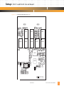
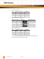
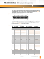
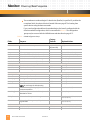
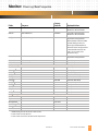
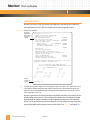
1
User’s Manual
from Emerson Network Power ™
Embedded Computing
PmT1 and PmE1: High Speed T1 and E1 Interface Module
December 2007
The information in this manual has been checked and is believed to be accurate and reliable.
HOWEVER, NO RESPONSIBILITY IS ASSUMED BY EMERSON NETWORK POWER, EMBEDDED
COMPUTING FOR ITS USE OR FOR ANY INACCURACIES. Specifications are subject to change
without notice. EMERSON DOES NOT ASSUME ANY LIABILITY ARISING OUT OF USE OR
OTHER APPLICATION OF ANY PRODUCT, CIRCUIT, OR PROGRAM DESCRIBED HEREIN. This
document does not convey any license under Emerson patents or the rights of others.
Emerson. Consider It Solved is a trademark, and Business-Critical Continuity, Emerson Network Power, and the Emerson Network Power logo are trademarks and service marks of
Emerson Network Power, Embedded Computing, Inc.
© 2007 Emerson Network Power, Embedded Computing, Inc.
Revision Level:
Principal Changes:
Date:
10002367-00
Original release
March 2001
10002367-01
RoHS 5-of6 compliance, ECR000272
March 2006
10002367-02
Artwork rev.-33
December 2007
Copyright © 2007 Emerson Network Power, Embedded Computing, Inc. All rights reserved.
Regulatory Agency Warnings & Notices
The Emerson PmT1 and PmE1 meets the requirements set forth by the Federal Communications Commission (FCC) in Title 47 of the Code of Federal Regulations. The following
information is provided as required by this agency.
This device complies with part 15 of the FCC Rules. Operation is subject to the following
two conditions: (1) This device may not cause harmful interference, and (2) this device
must accept any interference received, including interference that may cause undesired
operation.
FCC RULES AND REGULATIONS — PART 15
This equipment has been tested and found to comply with the limits for a Class A digital
device, pursuant to part 15 of the FCC Rules. These limits are designed to provide reasonable protection against harmful interference when the equipment is operated in a commercial environment. This equipment generates, uses and can radiate radio frequency energy
and, if not installed and used in accordance with the instructions, may cause harmful interference to radio communications. Operation of this equipment in a residential area is likely
to cause harmful interference, in which case the user will be required to correct the interference at his own expense.
Caution: Making changes or modifications to the PmT1 and PmE1 hardware without the explicit
consent of Emerson Network Power could invalidate the user’s authority to operate this
!
equipment.
EMC COMPLIANCE
The electromagnetic compatibility (EMC) tests used a PmT1 and PmE1 model that includes
a front panel assembly from Emerson Network Power.
Caution: For applications where the PmT1 and PmE1 is provided without a front panel, or where the
front panel has been removed, your system chassis/enclosure must provide the required
!
electromagnetic interference (EMI) shielding to maintain EMC compliance.
FCC RULES AND REGULATIONS — PART 68
This equipment complies with Part 68 of the FCC rules. There is a label on the PmT1 and
PmE1 board that contains the FCC registration number. If requested, this information must
be provided to the telephone company.
10002367-02
PmT1 and PmE1 User’s Manual
i
Regulatory Agency Warnings & Notices
(continued)
This board is designed to be connected to the telephone network or premises wiring using
a compatible modular jack which is Part 68 compliant. This board cannot be used on telephone company-provided coin service. Connection to Party Line Service is subject to state
tariffs.
If this board causes harm to the telephone network, the telephone company will notify you
in advance that temporary discontinuance of service may be required. If advance notice is
not practical, the telephone company will notify the customer as soon as possible. Also, you
will be advised of your right to file a complaint with the FCC if you believe it is necessary.
The telephone company may make changes in its facilities, equipment, operations, or procedures that could affect the operation of the equipment. If this happens, the telephone
company will provide advance notice in order for you to make the necessary modifications
in order to maintain uninterrupted service.
It is recommended that the customer install an AC surge arrestor in the AC outlet to which
this device is connected. This is to avoid damaging the equipment caused by local lightening strikes and other electrical surges.
The following table lists each applicable Facility Interface Code (FIC) along with the Service
Order Code (SOC) and connector jack type for the PmT1 and PmE1.
Board Name:
Facility Interface
Code (FIC):
FIC
Description:
Service Order
Code (SOC):
Jack
Type:
PmT1 and PmE1
04DU9.BN
1.54 Mbps AMI Superframe Format (SF) without
line power
6.0Na
RJ48C
04DU9.DN
1.544 Mbps SF and B8ZF without line power
04DU9.1KN
1.544 Mbps AMI ESF without line power
04DU9.1SN
1.544 Mbps AMI ESF and B8ZS without line power
a. Combinations of equipment provide full protection to digital service. Billing protection and encoded analog protection are provided
either by including auxiliary equipment within the registration envelope or by use of a separately registered device.
Note: The following information and instructions must be given to the final assembler/end user.
The mounting of the PmT1 and PmE1 in the final assembly must be made so that the PmT1
and PmE1 is isolated from exposure to hazardous voltages within the assembly. Adequate
separation and restraint of cables and cords must be provided.
The circuitry from the PmT1 and PmE1 to the telephone line must be provided in wiring
that carries no other circuitry that is specifically allowed in the rules, such as PR and PC
leads.
PC board traces carrying tip and ring leads shall have sufficient spacing to avoid surge
breakdown.
ii
PmT1 and PmE1 User’s Manual
10002367-02
Regulatory Agency Warnings & Notices
(continued)
Information shall be provided as to the power source requirements. See the PmT1 and
PmE1 power requirements in the hardware manual.
If the device is enclosed in an assembly, and not readily accessible, a label shall be placed on
the exterior of the cabinet listing the registration number of each PmT1 and PmE1 contained therein.
The final assembler shall provide, in the consumer instructions, all applicable Network Connection Information.
INDUSTRY CANADA RULES AND REGULATIONS — CS03
NOTICE: The Industry Canada label identifies certified equipment. This certification means
that the equipment meets certain telecommunications network protective, operational,
and safety requirements as prescribed in the appropriate Terminal Equipment Technical
Requirements document(s). The Department does not guarantee the equipment will operate to the user’s satisfaction.
Before installing this equipment, users should ensure that it is permissible to be connected
to the facilities of the local telecommunications company. The equipment must also be
installed using an acceptable method of connection. The customer should be aware that
compliance with the above conditions may not prevent degradation of service in some situations.
Repairs to certified equipment should be coordinated by a representative designated by
the supplier. Any repairs or alterations made by the user to this equipment, or equipment
malfunctions, may give the telecommunications company cause to request the user to disconnect the equipment.
Users should ensure for their own protection that the electrical ground connections of the
power utility, telephone lines, and internal metallic water pipe system, if present, are connected together. This precaution may be particularly important in rural areas.
Caution: Users should not attempt to make such connections themselves, but should contact the
appropriate electric inspection authority, or electrician as appropriate.
!
The standard connecting arrangement code (telephone jack type) for this equipment is
CA48C.
10002367-02
PmT1 and PmE1 User’s Manual
iii
Regulatory Agency Warnings & Notices
(continued)
EC Declaration of Conformity
According to EN 45014:1998
Manufacturer’s Name:
Emerson Network Power
Embedded Computing
Manufacturer’s Address:
8310 Excelsior Drive
Madison, Wisconsin 53717
Declares that the following product, in accordance with the requirements of 2004/108/EEC, EMC
Directive and 1999/5/EC, RTTE Directive and their amending directives,
Product:
PMC Module
Model Name/Number:
PmT1 and PmE1/01439143-xx
has been designed and manufactured to the following specifications:
EN55022:1998 Information Technology Equipment, Radio disturbance characteristics, Limits and
methods of measurement
EN55024:1998 Information Technology Equipment, Immunity characteristics, Limits and methods
of measurement
EN300386 V.1.3.1 Electromagnetic compatibility and radio spectrum matters (ERM);
Telecommunication network equipment; EMC requirements
As manufacturer we hereby declare that the product named above has been designed to comply
with the relevant sections of the above referenced specifications. This product complies with the
essential health and safety requirements of the EMC Directive and RTTE Directive. We have an internal production control system that ensures compliance between the manufactured products and
the technical documentation.
Bill Fleury
Compliance Engineer
Issue date: December 14, 2007
iv
PmT1 and PmE1 User’s Manual
10002367-02
Contents
1 Overview
5 Serial I/O
Components and Features . . . . . . . . . . . 1-1
Functional Overview . . . . . . . . . . . . . . . . 1-1
Physical Memory Map . . . . . . . . . . . . . . . 1-2
Additional Information . . . . . . . . . . . . . . 1-4
Product Certification . . . . . . . . . . . . . 1-4
RoHS Compliance. . . . . . . . . . . . . . . . 1-6
Terminology and Notation . . . . . . . . 1-6
Technical References. . . . . . . . . . . . . 1-6
2 Setup
Electrostatic Discharge . . . . . . . . . . . . . . 2-1
PmT1 and PmE1 Circuit Board . . . . . . . . 2-1
Connectors . . . . . . . . . . . . . . . . . . . . . 2-4
Installation . . . . . . . . . . . . . . . . . . . . . . . . . 2-4
PmT1 and PmE1 Setup . . . . . . . . . . . . . . 2-5
Power Requirements . . . . . . . . . . . . . 2-5
Environmental Considerations . . . . 2-6
Reset Methods . . . . . . . . . . . . . . . . . . . . . 2-6
Troubleshooting . . . . . . . . . . . . . . . . . . . . 2-6
Technical Support . . . . . . . . . . . . . . . 2-7
Product Repair . . . . . . . . . . . . . . . . . . 2-8
3 Central Processing Unit
MPC860P Initialization . . . . . . . . . . . . . . 3-1
MPC860P Exception Handling . . . . . . . . 3-3
CPU Interrupts . . . . . . . . . . . . . . . . . . 3-4
System Interface Unit (SIU). . . . . . . . . . . 3-4
Timebase Counter . . . . . . . . . . . . . . . 3-5
Decrementer Counter . . . . . . . . . . . . 3-5
Software Reset . . . . . . . . . . . . . . . . . . . . . 3-5
MPC860 Parallel Port configuration . . . 3-5
Optional BDM Header . . . . . . . . . . . . . . . 3-6
4 On-Card Memory
Configuration
Socketed Flash . . . . . . . . . . . . . . . . . . . . . 4-1
I2C EEPROM . . . . . . . . . . . . . . . . . . . . . . . . 4-1
I2C EEPROM Operation . . . . . . . . . . . 4-2
Emerson Memory Map . . . . . . . . . . . 4-2
On-card DRAM . . . . . . . . . . . . . . . . . . . . . 4-2
On-card Memory Sizing and Type . . 4-3
DRAM Timing . . . . . . . . . . . . . . . . . . . 4-3
10002367-02
The Communications Processor Module5-1
CPM Register Initialization Format . 5-2
RISC Controller. . . . . . . . . . . . . . . . . . 5-2
CPM Interrupt Handling . . . . . . . . . . 5-3
Dual-Port RAM . . . . . . . . . . . . . . . . . . 5-3
General Purpose Timers . . . . . . . . . . 5-4
Independent DMA (IDMA) Channels5-4
Serial DMA (SDMA) Channels . . . . . 5-4
MPC860P Serial Interface . . . . . . . . . . . . .5-4
Serial Communication Controllers
(SCC) . . . . . . . . . . . . . . . . . . . . . . . . . . . . . . . . . . 5-5
Serial Management Controllers
(SMC) . . . . . . . . . . . . . . . . . . . . . . . . . . . . . . . . . . 5-5
Time Slot Assigner (TSA) . . . . . . . . . 5-5
UART Baud Rate Selection . . . . . . . . . . . .5-6
Serial Connector Pin Assignments . . . . .5-7
6 TDM Interface
The T1 or E1 Line Interface . . . . . . . . . . . .6-4
Configuring the T1 or E1 Interface . . . . .6-5
The T1 FDL Interface . . . . . . . . . . . . . . . . .6-5
The Management Data Interface (MDI) .6-7
Front Panel I/O . . . . . . . . . . . . . . . . . . . . . .6-8
7 PMC/PCI Interface
PCI9060ES Register Map . . . . . . . . . . . . . .7-1
PCI Configuration Registers. . . . . . . 7-1
Local Configuration Registers . . . . . 7-2
Shared Runtime Registers . . . . . . . . 7-3
PCI9060ES Initialization . . . . . . . . . . . . . .7-3
Deadlocked Cycles . . . . . . . . . . . . . . 7-6
Retries on Local Direct Master
Cycles . . . . . . . . . . . . . . . . . . . . . . . . . . . . . . . . . .7-6
Retries on Direct Slave Cycles. .7-6
Assigning Priorities. . . . . . . . . . .7-6
Controlling Access Latency . . . . . . . 7-7
Avoiding the PCI9060ES Phantom
Read . . . . . . . . . . . . . . . . . . . . . . . . . . . . . . . . . . . 7-7
Managing Bandwidth . . . . . . . . . . . . 7-8
Bridge to Bridge Considerations . . . 7-8
PCI Interrupts . . . . . . . . . . . . . . . . . . . . . . .7-8
PCI Bus Interface . . . . . . . . . . . . . . . . 7-8
PMC Connector Pin Assignments . . . . . .7-8
PCI Bus Control Signals . . . . . . . . . . 7-10
PmT1 and PmE1 User’s Manual
v
8 Monitor
Power-up/Reset Sequence . . . . . . . . . . . .8-1
Start-up Display . . . . . . . . . . . . . . . . . . . . .8-4
Command-line History . . . . . . . . . . . . . . .8-5
Command-line Editor . . . . . . . . . . . . . . . .8-5
Initializing Memory . . . . . . . . . . . . . . . . . .8-6
Command Syntax . . . . . . . . . . . . . . . . . . . .8-6
Initializing Memory . . . . . . . . . . . . . . . . . .8-7
Command Syntax . . . . . . . . . . . . . . . . . . . .8-7
Typographic Conventions . . . . . . . . 8-7
Boot Commands. . . . . . . . . . . . . . . . . . . . .8-7
bootbus . . . . . . . . . . . . . . . . . . . . . . . . 8-7
booteprom . . . . . . . . . . . . . . . . . . . . . 8-8
bootrom. . . . . . . . . . . . . . . . . . . . . . . . 8-9
bootserial. . . . . . . . . . . . . . . . . . . . . . . 8-9
Help Commands. . . . . . . . . . . . . . . . . . . 8-10
help. . . . . . . . . . . . . . . . . . . . . . . . . . .8-10
Memory/Register Commands . . . . . . . 8-10
checksummem. . . . . . . . . . . . . . . . .8-10
clearmem . . . . . . . . . . . . . . . . . . . . .8-10
cmpmem . . . . . . . . . . . . . . . . . . . . . .8-10
copymem . . . . . . . . . . . . . . . . . . . . .8-10
displaymem . . . . . . . . . . . . . . . . . . .8-11
fillmem. . . . . . . . . . . . . . . . . . . . . . . .8-11
findmem . . . . . . . . . . . . . . . . . . . . . .8-11
findnotmem . . . . . . . . . . . . . . . . . . .8-11
findstr. . . . . . . . . . . . . . . . . . . . . . . . .8-11
readmem . . . . . . . . . . . . . . . . . . . . . .8-11
setmem . . . . . . . . . . . . . . . . . . . . . . .8-12
swapmem . . . . . . . . . . . . . . . . . . . . .8-12
testmem . . . . . . . . . . . . . . . . . . . . . .8-12
um. . . . . . . . . . . . . . . . . . . . . . . . . . . .8-12
writemem . . . . . . . . . . . . . . . . . . . . .8-12
writestr. . . . . . . . . . . . . . . . . . . . . . . .8-13
NVRAM Commands . . . . . . . . . . . . . . . . 8-13
nvdisplay . . . . . . . . . . . . . . . . . . . . . .8-13
nvinit . . . . . . . . . . . . . . . . . . . . . . . . .8-14
nvopen . . . . . . . . . . . . . . . . . . . . . . . .8-14
nvset. . . . . . . . . . . . . . . . . . . . . . . . . .8-14
nvupdate . . . . . . . . . . . . . . . . . . . . . .8-15
Configuring the Default Boot
Device . . . . . . . . . . . . . . . . . . . . . . . . . . . . . . . .8-15
Power-up Diagnostic/Test Commands 8-17
cachetest . . . . . . . . . . . . . . . . . . . . . .8-18
eepromtest . . . . . . . . . . . . . . . . . . . .8-18
memtest . . . . . . . . . . . . . . . . . . . . . .8-18
Remote Host Commands . . . . . . . . . . . 8-18
call. . . . . . . . . . . . . . . . . . . . . . . . . . . .8-19
vi
PmT1 and PmE1 User’s Manual
10002367-02
download . . . . . . . . . . . . . . . . . . . . . 8-19
Binary Download Format . . . . . . . . 8-19
transmode . . . . . . . . . . . . . . . . . . . . 8-20
Configuring the Download Port . . 8-20
Hex-Intel Format . . . . . . . . . . . . . . . 8-21
Extended Address Record . . . . . . . 8-21
Data Record . . . . . . . . . . . . . . . . . . . 8-22
End-of-file Record . . . . . . . . . . . . . . 8-22
Motorola S-record Format . . . . . . . 8-24
S0-records (User Defined) . . . . . . . 8-24
S1-S2-and S3-records
(Data Records) . . . . . . . . . . . . . . . . . . . . . . . . . 8-25
S5-records (Data Count Records) . 8-25
S7-S8-and S9-records (Termination and
Start Address Records) . . . . . . . . . . . . . . . . . . 8-26
Utilities . . . . . . . . . . . . . . . . . . . . . . . . . . . 8-27
configboard . . . . . . . . . . . . . . . . . . . 8-27
Arithmetic Commands . . . . . . . . . . . . . 8-27
add . . . . . . . . . . . . . . . . . . . . . . . . . . . 8-27
div. . . . . . . . . . . . . . . . . . . . . . . . . . . . 8-27
mul . . . . . . . . . . . . . . . . . . . . . . . . . . . 8-28
rand . . . . . . . . . . . . . . . . . . . . . . . . . . 8-28
sub . . . . . . . . . . . . . . . . . . . . . . . . . . . 8-28
Errors and Screen Messages . . . . . . . . . 8-28
Monitor Function Reference . . . . . . . . 8-29
PmT1 and PmE1-Specific Functions . . 8-30
ChangeBaud . . . . . . . . . . . . . . . . . . . 8-30
EEPROMAcc . . . . . . . . . . . . . . . . . . . 8-30
getchar . . . . . . . . . . . . . . . . . . . . . . . 8-30
InitBoard . . . . . . . . . . . . . . . . . . . . . . 8-31
Misc . . . . . . . . . . . . . . . . . . . . . . . . . . 8-31
NvHkOffset . . . . . . . . . . . . . . . . . . . . 8-32
NvRamAcc . . . . . . . . . . . . . . . . . . . . 8-32
SetUnExpIntFunct . . . . . . . . . . . . . . 8-33
MPC860P-Specific Functions . . . . . . . . 8-33
Cache . . . . . . . . . . . . . . . . . . . . . . . . . 8-33
Exceptions. . . . . . . . . . . . . . . . . . . . . 8-33
Interrupts . . . . . . . . . . . . . . . . . . . . . 8-35
Status. . . . . . . . . . . . . . . . . . . . . . . . . 8-36
Standard Monitor Functions. . . . . . . . . 8-36
atoh . . . . . . . . . . . . . . . . . . . . . . . . . . 8-36
BootUp . . . . . . . . . . . . . . . . . . . . . . . 8-37
InitFifo . . . . . . . . . . . . . . . . . . . . . . . . 8-38
IsLegal . . . . . . . . . . . . . . . . . . . . . . . . 8-38
MemMng. . . . . . . . . . . . . . . . . . . . . . 8-39
NVSupport . . . . . . . . . . . . . . . . . . . . 8-40
Seed . . . . . . . . . . . . . . . . . . . . . . . . . . 8-42
Serial . . . . . . . . . . . . . . . . . . . . . . . . . 8-42
Contents
(continued)
TestSuite . . . . . . . . . . . . . . . . . . . . . .8-44
xprintf. . . . . . . . . . . . . . . . . . . . . . . . .8-45
10002367-02
9 Acronyms
PmT1 and PmE1 User’s Manual
vii
Contents
viii
(continued)
PmT1 and PmE1 User’s Manual
10002367-02
Figures
Figure 1-1:
General System Block Diagram. . . . . . . . . . . . . . . . . . . . . . . . . . . . . . . . . . . . . . . . . . . . . . 1-2
Figure 1-2:
Physical Memory Map. . . . . . . . . . . . . . . . . . . . . . . . . . . . . . . . . . . . . . . . . . . . . . . . . . . . . . 1-3
Figure 2-1:
PmT1 and PmE1 Front Panel . . . . . . . . . . . . . . . . . . . . . . . . . . . . . . . . . . . . . . . . . . . . . . . . 2-1
Figure 2-2:
Component Map, Top (rev. 33) . . . . . . . . . . . . . . . . . . . . . . . . . . . . . . . . . . . . . . . . . . . . . 2-2
Figure 2-3:
Component Map, Bottom (rev. 33) . . . . . . . . . . . . . . . . . . . . . . . . . . . . . . . . . . . . . . . . . . 2-3
Figure 2-4:
PmT1 and PmE1 Installation . . . . . . . . . . . . . . . . . . . . . . . . . . . . . . . . . . . . . . . . . . . . . . . . 2-5
Figure 2-5:
Serial Number and Product ID on Bottom Side . . . . . . . . . . . . . . . . . . . . . . . . . . . . . . . . 2-8
Figure 3-1:
Processor BDM Header. . . . . . . . . . . . . . . . . . . . . . . . . . . . . . . . . . . . . . . . . . . . . . . . . . . . . 3-7
Figure 6-1:
TDM and FDL Connectivity Diagram . . . . . . . . . . . . . . . . . . . . . . . . . . . . . . . . . . . . . . . . . 6-3
Figure 6-2:
MDI Interface Protocol . . . . . . . . . . . . . . . . . . . . . . . . . . . . . . . . . . . . . . . . . . . . . . . . . . . . . 6-7
Figure 6-3:
Front Panel I/O Connectors, P1 and P2 . . . . . . . . . . . . . . . . . . . . . . . . . . . . . . . . . . . . . . . 6-8
Figure 6-4:
Front Panel I/O Cable Assembly (C308A009-05). . . . . . . . . . . . . . . . . . . . . . . . . . . . . . . 6-9
Figure 7-1:
PMC Interface Connectors (P11, P12, P14). . . . . . . . . . . . . . . . . . . . . . . . . . . . . . . . . . . . 7-9
Figure 8-1:
Monitor Start-up Display . . . . . . . . . . . . . . . . . . . . . . . . . . . . . . . . . . . . . . . . . . . . . . . . . . . 8-4
10002367-02
PmT1 and PmE1 User’s Manual
ix
(blank page)
x
PmT1 and PmE1 User’s Manual
10002367-02
Tables
Table 1-1:
Address Summary . . . . . . . . . . . . . . . . . . . . . . . . . . . . . . . . . . . . . . . . . . . . . . . . . . . . . . . . . 1-4
Table 1-2:
MTBF Hours . . . . . . . . . . . . . . . . . . . . . . . . . . . . . . . . . . . . . . . . . . . . . . . . . . . . . . . . . . . . . . 1-4
Table 1-3:
Regulatory Agency Compliance — T1. . . . . . . . . . . . . . . . . . . . . . . . . . . . . . . . . . . . . . . . . 1-5
Table 1-4:
Regulatory Agency Compliance — E1 . . . . . . . . . . . . . . . . . . . . . . . . . . . . . . . . . . . . . . . . . 1-5
Table 1-5:
Technical References . . . . . . . . . . . . . . . . . . . . . . . . . . . . . . . . . . . . . . . . . . . . . . . . . . . . . . 1-6
Table 2-1:
Circuit Board Dimensions. . . . . . . . . . . . . . . . . . . . . . . . . . . . . . . . . . . . . . . . . . . . . . . . . . . 2-1
Table 2-2:
Power Requirements . . . . . . . . . . . . . . . . . . . . . . . . . . . . . . . . . . . . . . . . . . . . . . . . . . . . . . 2-6
Table 2-3:
Environmental Requirements . . . . . . . . . . . . . . . . . . . . . . . . . . . . . . . . . . . . . . . . . . . . . . . 2-6
Table 3-1:
MPC860P Features . . . . . . . . . . . . . . . . . . . . . . . . . . . . . . . . . . . . . . . . . . . . . . . . . . . . . . . . 3-1
Table 3-2:
MPC860P Special Purpose Register Initialization. . . . . . . . . . . . . . . . . . . . . . . . . . . . . . . 3-2
Table 3-3:
MPC860P Internal Register Initialization. . . . . . . . . . . . . . . . . . . . . . . . . . . . . . . . . . . . . . 3-2
Table 3-4:
MPC860P Exceptions . . . . . . . . . . . . . . . . . . . . . . . . . . . . . . . . . . . . . . . . . . . . . . . . . . . . . . 3-3
Table 3-5:
MPC860P SIU Register Block Map. . . . . . . . . . . . . . . . . . . . . . . . . . . . . . . . . . . . . . . . . . . . 3-4
Table 3-6:
MPC860P Ports A and C . . . . . . . . . . . . . . . . . . . . . . . . . . . . . . . . . . . . . . . . . . . . . . . . . . . . 3-6
Table 3-7:
Processor BDM Pin Assignments . . . . . . . . . . . . . . . . . . . . . . . . . . . . . . . . . . . . . . . . . . . . 3-7
Table 4-1:
I2C EEPROM Registers . . . . . . . . . . . . . . . . . . . . . . . . . . . . . . . . . . . . . . . . . . . . . . . . . . . . . 4-1
Table 4-2:
I2C EEPROM Memory Map . . . . . . . . . . . . . . . . . . . . . . . . . . . . . . . . . . . . . . . . . . . . . . . . . . 4-2
Table 4-3:
RAM Acess Time. . . . . . . . . . . . . . . . . . . . . . . . . . . . . . . . . . . . . . . . . . . . . . . . . . . . . . . . . . . 4-3
Table 5-1:
MPC860P CPM Register Block Map . . . . . . . . . . . . . . . . . . . . . . . . . . . . . . . . . . . . . . . . . . 5-1
Table 5-2:
CPM Initialization Values . . . . . . . . . . . . . . . . . . . . . . . . . . . . . . . . . . . . . . . . . . . . . . . . . . . 5-2
Table 5-3:
RISC Controller Processing Priority. . . . . . . . . . . . . . . . . . . . . . . . . . . . . . . . . . . . . . . . . . . 5-2
Table 5-4:
Asynchronous Baud Rates (16X oversample). . . . . . . . . . . . . . . . . . . . . . . . . . . . . . . . . . 5-6
Table 5-5:
Synchronous Baud Rates . . . . . . . . . . . . . . . . . . . . . . . . . . . . . . . . . . . . . . . . . . . . . . . . . . . 5-7
Table 5-6:
P14, P0, P2 Pin Assignments . . . . . . . . . . . . . . . . . . . . . . . . . . . . . . . . . . . . . . . . . . . . . . . . 5-7
Table 6-1:
TDM to T1E1 Port Connections for TDMB (P1). . . . . . . . . . . . . . . . . . . . . . . . . . . . . . . . . 6-1
Table 6-2:
T1E1 Signals from Transceiver, P1 . . . . . . . . . . . . . . . . . . . . . . . . . . . . . . . . . . . . . . . . . . . 6-2
Table 6-3:
TDM to T1E1 Port Connections for TDMA (P2) . . . . . . . . . . . . . . . . . . . . . . . . . . . . . . . . 6-2
Table 6-4:
T1E1 Signals from Transceiver, P2 . . . . . . . . . . . . . . . . . . . . . . . . . . . . . . . . . . . . . . . . . . . 6-2
Table 6-5:
FDL QUICC Port Assignments . . . . . . . . . . . . . . . . . . . . . . . . . . . . . . . . . . . . . . . . . . . . . . . 6-6
Table 6-6:
MDI Port Connections. . . . . . . . . . . . . . . . . . . . . . . . . . . . . . . . . . . . . . . . . . . . . . . . . . . . . . 6-7
Table 6-7:
MDI Bit Field Format . . . . . . . . . . . . . . . . . . . . . . . . . . . . . . . . . . . . . . . . . . . . . . . . . . . . . . . 6-8
Table 6-8:
Compu-Shield to RJ45 Pin Assignments . . . . . . . . . . . . . . . . . . . . . . . . . . . . . . . . . . . . . . 6-9
Table 7-1:
PCI Configuration Registers. . . . . . . . . . . . . . . . . . . . . . . . . . . . . . . . . . . . . . . . . . . . . . . . . 7-1
Table 7-2:
Local Configuration Registers . . . . . . . . . . . . . . . . . . . . . . . . . . . . . . . . . . . . . . . . . . . . . . . 7-2
Table 7-3:
Shared Runtime Registers . . . . . . . . . . . . . . . . . . . . . . . . . . . . . . . . . . . . . . . . . . . . . . . . . . 7-3
Table 7-4:
PCI9060ES PCI Configuration Register Initialization . . . . . . . . . . . . . . . . . . . . . . . . . . . . 7-4
Table 7-5:
PCI9060ES Local Configuration Register Initialization . . . . . . . . . . . . . . . . . . . . . . . . . . 7-5
Table 7-6:
PCI9060ES Shared Runtime Register Initialization . . . . . . . . . . . . . . . . . . . . . . . . . . . . . 7-6
Table 7-7:
PCI9060ES Bus Priority Control. . . . . . . . . . . . . . . . . . . . . . . . . . . . . . . . . . . . . . . . . . . . . . 7-7
Table 7-8:
PCI-to-Local Slave Access Timing . . . . . . . . . . . . . . . . . . . . . . . . . . . . . . . . . . . . . . . . . . . . 7-8
10002367-02
PmT1 and PmE1 User’s Manual
xi
xii
Table 7-9:
Connector P11 and P12 Pin Assignments . . . . . . . . . . . . . . . . . . . . . . . . . . . . . . . . . . . . . 7-9
Table 8-1:
NVRAM Configuration Groups . . . . . . . . . . . . . . . . . . . . . . . . . . . . . . . . . . . . . . . . . . . . . . 8-2
Table 8-2:
Device Download Format . . . . . . . . . . . . . . . . . . . . . . . . . . . . . . . . . . . . . . . . . . . . . . . . . . 8-9
Table 8-3:
NVRAM Power-up Diagnostic PASS/FAIL Flags . . . . . . . . . . . . . . . . . . . . . . . . . . . . . . . 8-17
Table 8-4:
PLX Mailbox 0 Sequence and Fail Mask Bits . . . . . . . . . . . . . . . . . . . . . . . . . . . . . . . . . . 8-17
Table 8-5:
Error and Screen Messages . . . . . . . . . . . . . . . . . . . . . . . . . . . . . . . . . . . . . . . . . . . . . . . . 8-28
Table 8-6:
Assigned Exception Vectors . . . . . . . . . . . . . . . . . . . . . . . . . . . . . . . . . . . . . . . . . . . . . . . 8-34
Table 8-7:
IsLegal Function Types . . . . . . . . . . . . . . . . . . . . . . . . . . . . . . . . . . . . . . . . . . . . . . . . . . . . 8-39
Table 8-8:
NVOp Command . . . . . . . . . . . . . . . . . . . . . . . . . . . . . . . . . . . . . . . . . . . . . . . . . . . . . . . . . 8-41
Table 8-9:
NVOP Error Codes . . . . . . . . . . . . . . . . . . . . . . . . . . . . . . . . . . . . . . . . . . . . . . . . . . . . . . . . 8-42
PmT1 and PmE1 User’s Manual
10002367-02
Registers
Register 4-1:
Board Configuration 0 (BCR), 0x010 . . . . . . . . . . . . . . . . . . . . . . . . . . . . . . . . . . . . . . . . . 4-3
10002367-02
PmT1 and PmE1 User’s Manual
i
(blank page)
ii
PmT1 and PmE1 User’s Manual
10002367-02
Section 1
Overview
The PmT1 and PmE1 is a single width PMC module designed to provide high-speed T1 and
E1 interfaces for PMC-compatible baseboards. The design is based on the Freescale™
MPC860P PowerQUICC™ microprocessor and the PLX Technology PCI9060ES bus interface
controller. The PmT1 has two standard landed T1 channels, and the PmE1 has two standard
landed E1 channels. An optional EIA-422 port is available.
COMPONENTS AND FEATURES
The following is a brief summary of the PmT1 and PmE1 hardware components and features:
CPU: The CPU for the PmT1 and PmE1 is the Freescale MPC860P PowerQUICC 32-bit microprocessor chip running at 80MHz. See Chapter 3 for processor features.
RAM: The PmT1 and PmE1 module is populated with 16 megabytes of 32-bit wide DRAM.
Flash: The PmT1 and PmE1 module has a 32-pin PLCC flash socket with a 512-kilobyte flash capacity.
Serial I/O: The PmT1 and PmE1 module has two EIA-232 I/O ports implemented with two serial management controllers (SMCs). If the second E1 channel is not required, the PmE1 can be factory configured to additionally provide a single EIA-422 serial port.
T1E1: The PmT1 is factory configured to support the T1 channel using the Dallas Semiconductor
DS2151Q controller. The PmE1 is factory configured to support the E1 channel using the
Dallas Semiconductor DS2153Q controller.
PCI Bus: The PLX Technology PCI9060ES controls the Peripheral Component Interconnect (PCI) bus.
The PmT1 and PmE1 modules appear as peripheral cards to PCI.
FUNCTIONAL OVERVIEW
The following block diagram provides a functional overview for the PmT1 and PmE1:
10002367-02
PmT1 and PmE1 User’s Manual
1-1
Overview:
Physical Memory Map
Figure 1-1: General System Block Diagram
PmT1 or PmE1
Channel 1
CPU
MPC860P
System Interface Unit (SIU)
PmT1 or PmE1
Channel 2 or EIA422 Port
32-Bit Bus
Power PC
Processor Core
PMC Connectors
P14
Memory Controller
Internal
External
Bus Interface Bus Interface
Unit
Unit
System Functions
Real-Time Clock
PCMCIA-ATA Interface
Communcations
Processor Module (CPM)
EIA232 Console
and Download
Serial Ports
I2C
A32/D32
DRAM
16 megabytes
Flash/ROM
Socket
512 kilobytes
PCI Controller
PCI90x0
32
PCI
A20/D8
A21/D32
PMC Connectors
P11, P12
EEPROM
2 kilobytes
1
Serial
EEPROM
128 bytes
PHYSICAL MEMORY MAP
The physical memory map of the PmT1 and PmE1 is depicted in Fig. 1-2. Information on particular portions of the memory map can be found in later sections of this manual. See
Table 1-1 for a list of these references.
1-2
PmT1 and PmE1 User’s Manual
10002367-02
Overview:
Physical Memory Map
Figure 1-2: Physical Memory Map
Hex Address
FFFF,FFFF
FFF0,0000
Flash/ROM Socket
CPU Registers
FF00,0000
Reserved
C101,0000
C100,0000
C000,0200
C000,0180
C000,0080
C000,0000
PMC/PCI Interface Registers
Reserved
Board Configuration Register
Reserved
IDs / Interrupts
Reserved
8000,0000
PCI I/O Space
6000,0000
PCI Memory Space
4000,0000
Reserved
0100,0000
DRAM
0000,0000
10002367-02
PmT1 and PmE1 User’s Manual
1-3
Overview:
Additional Information
Table 1-1: Address Summary
Physical Address
(hex):
Access
Mode:
Description:
See
Page:
FFF0,0000
R
Flash/ROM Socket
4-1
FF00,0000
R/W
CPU registers
3-2
C101,0000
—
reserved
—
C100,0000
R/W
PMC/PCI Interface registers
7-2
C000,0200
—
reserved
—
C000,0180
R
Board Configuration register
4-3
C000,0080
—
reserved
—
C000,000C
R
Conventional Interrupt register
3-4
C000,0000
R
Interrupt Vector register
3-4
8000,0000
—
reserved
—
6000,0000
R/W
PCI I/O Space
7-2
4000,000
R/W
PCI Memory Space
7-2
C101,0000
—
reserved
—
0000,0000
R/W
DRAM
4-2
ADDITIONAL INFORMATION
This section lists the PmT1 and PmE1 hardware’s regulatory certifications and briefly discusses the terminology and notation conventions used in this manual. It also lists general
technical references.
Mean time between failures (MTBF) is listed in the following table:
Table 1-2: MTBF Hours
Product
Calculation Method:
PmT1
Bellcore Issue 5
Hours:
344,234
PmE1
Telecordia Issue 1
1,333,573
Product Certification
The PmT1 and PmE1 hardware has been tested to comply with various safety, immunity,
and emissions requirements as specified by the Federal Communications Commission
(FCC), Underwriters Laboratories (UL), and others. The following table summarizes this
compliance:
1-4
PmT1 and PmE1 User’s Manual
10002367-02
Overview:
Additional Information
Table 1-3: Regulatory Agency Compliance — T1
Type:
Specification:
Safety
UL60950-1, CSA C22.2 No. 60950-1-03, 1st Edition – Safety of
Information Technology Equipment, including Electrical Business
Equipment (BI-National)
Telecom
FCC Part 68 – Title 47, Code of Federal Regulations, Radio
Frequency Devices
Global IEC – CB Scheme Report IEC 60950, all country deviations
IC CS03 – Radiated and Conducted Emissions, Canada
EMC
FCC Part 15, Class A – Title 47, Code of Federal Regulations, Radio
Frequency Devices
ICES 003, Class A – Radiated and Conducted Emissions, Canada
Table 1-4: Regulatory Agency Compliance — E1
Type:
Specification:
Safety
IEC60950/EN60950 – Safety of Information Technology Equipment
(Western Europe)
Telecom
CTR012 – Business Telecommunications; Open Network Provision
technical requirements; 2048 kbits/s digital unstructured leased line
attachment requirements for terminal equipment.
CTR013 – Business Telecommunications Open Network Provision
technical requirement, 2048 kbits/s structured, leased line attachment
requirements for terminal equipment.
EMC
EN55022 – Information Technology Equipment, Radio Disturbance
Characteristics, Limits and Methods of Measurement
EN55024 – Information Technology Equipment, Immunity
Characteristics, Limits and Methods of Measurement
ETSI EN300386 – Electromagnetic Compatibility and Radio Spectrum
Matters (ERM), Telecommunication Network Equipment,
Electromagnetic Compatibility (EMC) Requirements
Emerson maintains test reports that provide specific information regarding the methods
and equipment used in compliance testing. Unshielded external I/O cables, loose screws, or
a poorly grounded chassis may adversely affect the PmT1 and PmE1 hardware’s ability to
comply with any of the stated specifications.
The UL web site at ul.com has a list of Emerson’s UL certifications. To find the list, search in
the online certifications directory using Emerson’s UL file number, E190079. There is a list
for products distributed in the United States, as well as a list for products shipped to Canada. To find the PmT1 and PmE1, search in the list for 01439143-xx, where xx changes with
each revision of the printed circuit board.
10002367-02
PmT1 and PmE1 User’s Manual
1-5
Overview:
Additional Information
RoHS Compliance
The PmT1 and PmE1 are compliant with the European Union’s RoHS (Restriction of Use of
Hazardous Substances) directive created to limit harm to the environment and human
health by restricting the use of harmful substances in electrical and electronic equipment.
Effective July 1, 2006, RoHS restricts the use of six substances: cadmium (Cd), mercury
(Hg), hexavalent chromium (Cr (VI)), polybrominated biphenyls (PBBs), polybrominated
diphenyl ethers (PBDEs) and lead (Pb). Configurations that are 5-of-6 are built with tin-lead
solder per the lead-in-solder RoHS exemption.
To obtain a certificate of conformity (CoC) for the PmT1 and PmE1 modules, send an
e-mail to [email protected] or call 1-800-356-9602. Have the part number(s) (e.g.,
C000####-##) for your configuration(s) available when contacting Emerson.
Terminology and Notation
Active low signals: An active low signal is indicated with an asterisk * after the signal name.
Byte, word: Throughout this manual byte refers to 8 bits, word refers to 16 bits, and long word refers to
32 bits, double long word refers to 64 bits.
PLD: This manual uses the acronym, PLD, as a generic term for programmable logic device (also
known as FPGA, CPLD, EPLD, etc.).
Radix 2 and 16: Hexadecimal numbers end with a subscript 16. Binary numbers are shown with a
subscript 2.
Technical References
Further information on basic operation and programming of the PmT1 and PmE1 components can be found in the following documents:
Table 1-5: Technical References
Device / Interface:
Document: 1
Controller, T1/E1
DS2153Q, E1 Single Chip Transceiver Data Sheet
(Dallas Semiconductor, REV: 01106)
DS2151Q, T1 Single Chip Transceiver Data Sheet
(Dallas Semiconductor, REV: 011706)
Application Note 342; DS2151, DS2153 Initialization and Programming
(Dallas Semiconductor, 102899)
http://www.maxim-ic.com/
CPU
1-6
PmT1 and PmE1 User’s Manual
MPC860P PowerQUICC™ Technical Summary
(Freescale Semiconductor, 07/2004 Rev. 3)
http://www.freescale.com/
10002367-02
Overview:
Additional Information
Device / Interface:
Document: 1
EEPROM
CAT93C86 (Die Rev. C) 16-Bit Microwire Serial EEPROM
(Catalyst l Semiconductor, Inc.., Doc. No. 1091, Rev. O, 10/13/06)
http://www.catsemi.com/
PCI
PCI Local Bus Specification
(PCI Special Interest Group, Revision 2.1 1995)
http://www.pcisig.com/
(continued)
PCI9060ES PCI Bus Master Interface Chip for Adapters and Embedded
Systems–data sheet
(Mountain View, CA: PLX Technology, Inc., December1995 VERSION 1.2)
http://www.plxtech.com/
PMC
Draft Standard for a Common Mezzanine Card Family: CMC P1386/Draft 2.0
April 4, 1995
(IEEE:New York, NY)
Draft Standard Physical and Environmental Layers for PCI Mezzanine Cards:
PMC P1386.1/Draft 2.0 April 4, 1995
(IEEE: New York, NY)
http://www.ieee.org/
Serial Interface
EIA Subcommittee TR-30.2 on Interface, EIA Standard RS-232-D
(Electronic Industries Association, August 1969)
http://www.eia.org/
1. Frequently, the most current information regarding addenda/errata for specific documents may be
found on the corresponding web site.
10002367-02
PmT1 and PmE1 User’s Manual
1-7
Overview:
1-8
Additional Information
PmT1 and PmE1 User’s Manual
10002367-02
Section 2
Setup
This chapter describes the physical layout of the boards, the setup process, and how to
check for proper operation once the boards have been installed. This chapter also includes
troubleshooting, service, and warranty information.
ELECTROSTATIC DISCHARGE
Before you begin the setup process, please remember that electrostatic discharge (ESD) can
easily damage the components on the PmT1 and PmE1 hardware. Electronic devices, especially those with programmable parts, are susceptible to ESD, which can result in operational failure. Unless you ground yourself properly, static charges can accumulate in your
body and cause ESD damage when you touch the board.
Caution: Use proper static protection and handle the PmT1 and PmE1 board only when absolutely
necessary. Always wear a wriststrap to ground your body before touching a board. Keep
!
your body grounded while handling the board. Hold the board by its edges–do not touch
any components or circuits. When the board is not in an enclosure, store it in a staticshielding bag.
To ground yourself, wear a grounding wriststrap. Simply placing the board on top of a staticshielding bag does not provide any protection–place it on a grounded dissipative mat. Do
not place the board on metal or other conductive surfaces.
PMT1 AND PME1 CIRCUIT BOARD
The PmT1 and PmE1 circuit board is a PMC module assembly. It uses an eight-layer printed
circuit board with the following dimensions:
Table 2-1: Circuit Board Dimensions
Width:
Depth:
Height:
5.86 in. (148.8 mm)
2.913 in. (74.0 mm)
.39 in. (10.0 mm)
The following figures show the front panel and component maps for the PmT1 and PmE1
circuit board.
TDM B
TDM A
Figure 2-1: PmT1 and PmE1 Front Panel
10002367-02
PmT1 and PmE1 User’s Manual
2-1
Setup:
PmT1 and PmE1 Circuit Board
Figure 2-2: Component Map, Top (rev. 33)
C9
C7
C8
U4
T1/E1
U101
C12 C13
U10
Y4
RN1
U6
R7
C19
L2
L1 C20
C21
C24 R11 R10 C22
U12
U11
C14
Y3
C18 C17 C15 R9
Y6
U7
Y2
Y5
U100
P11
C29
U16
MPC860
C23
Y7
RN2
U18
U13
PCI90x0
U14
U15
PmT1 and PmE1 User’s Manual
X5
R12
C25
U17
C26 C27
U19
C28
C30
P12
2-2
C16
Y1
C6 S1
U20
U21
C10
U22
P14
10002367-02
R13
R14
U3
T1/E1
F13
F15
C5
C4
R1
S2
C3
U2
U9
C1 C2
F9
F11
R5
R6
R8
F8
F6
U1
U5
F2 F3 F4
P2
F7
F5
F1
U8
P1
Setup:
PmT1 and PmE1 Circuit Board
Figure 2-3: Component Map, Bottom (rev. 33)
R20 CR1/CR4
R21
CR2/CR6 CR5
U24
U29
U28
R27
R28
R34
R35
R2
R3
R4
C36
R40 R39
C35 C34
C45
C40
C44 C42 C41
R15
U32
C48
R59 R57
R60 R58
C52
C53
CR10 C56
CR11
R63
R66
C55
C66
C58
R69 R68
R43 R42
R47
R48 R46
R54 R53
C57
R67
R70
P3
R16
R74
R73
R75
R72 R71
R17
C67
C59
R64
R65
C64
R61
C63
C62
C61
R62
C54 C51
R52
R55
R56
C47
U31
C65
R45
R41
CR9
C60
U26
C43
C37
U27
R51
R50
R49
C39 C38
C46
R44
U30
U23
R36 R24
R33 R23
U25
CR3
CR7
C32
C31
R25
R30 R29
CR8
C50
C49
R22
R31
R32
R37
R38
R18
C11
C33
R26
R19
C68
590-
YYYYY
10002367-02
D
10001234-AA
PmT1 and PmE1 User’s Manual
2-3
Setup:
Installation
Connectors
The PmT1 and PmE1 circuit board has various connectors (see the figures beginning on
page 2-2), summarized as follows:
P1/P2: These connectors are installed for the PmT1 front panel I/O configurations. See Chapter 6
for pin assignments.
P3: This is the optional 10-pin BDM JTAG header for viewing processor functions. See Table 3-7
for pin assignments.
P11/P12: These provide a 32-bit PCI interface between the module and the PMC baseboard. Pin
assignments are shown in Chapter 7.
P14: This is the I/O connector for the EIA-422 and EIA-232 serial ports. See Chapter 5 for pin
assignments.
INSTALLATION
The PmT1 and PmE1 module may be installed in either expansion site on the baseboard. To
attach the module to your baseboard, follow these steps:
1 Remove the loosely installed screws from the standoffs on the PmT1 and PmE1 module.
2 Line up the P11, P12, and P14 connectors and the 5V keying hole with the PMC connectors
and the keying pin on the baseboard. Press the module into place, making sure that the
connectors are firmly mated and the module front panel is fully seated in the baseboard
front panel.
3 From the back of the baseboard, insert and tighten the two screws in the standoffs closest
to the PMC connectors.
2-4
PmT1 and PmE1 User’s Manual
10002367-02
Setup:
PmT1 and PmE1 Setup
Figure 2-4: PmT1 and PmE1 Installation
Voltage key
Tighten these two screws first.
4 Insert and tighten the two remaining screws.
PMT1 AND PME1 SETUP
You need the following items to set up and check the operation of the Emerson PmT1 and
PmE1:
❐ Five-volt compatible PMC baseboard
❐ Chassis and power supply
❐ Serial interface cable for EIA-232 port, Emerson part #C0006322-xx0
❐ Two Compu-shield to RJ45 cable assemblies (Emerson part number C308A009-xx) for
front panel I/O configurations
❐ Computer terminal
Save the antistatic bag and box for future shipping or storage.
Caution: Do not install the board in a rack or remove the board from a rack while power is applied, at
risk of damage to the board.
!
Power Requirements
The Emerson PmT1 and PmE1 circuit board typically requires 6.7 watts maximum.
10002367-02
PmT1 and PmE1 User’s Manual
2-5
Setup:
Reset Methods
Table 2-2: Power Requirements
Volts:
Range (volts):
Maximum Current:
+5
+/- 5%
1.16 A, typical1
1. Running on-card memory test.
The exact power requirements for the PmT1 and PmE1 circuit board depend upon the specific configuration of the board, including the CPU frequency and amount of memory
installed on the board. Please contact Emerson Technical Support at 1-800-327-1251 if you
have specific questions regarding the board’s power requirements.
Environmental Considerations
As with any printed circuit board, be sure that air flow to the board is adequate. Chassis constraints and other factors greatly affect the air flow rate. The environmental requirements
are listed in Table 2-3.
Table 2-3: Environmental Requirements
Environment:
Range:
Relative Humidity:
Operating Temperature
0° to +55° Centigrade, ambient
(at board)
Not to exceed 95% (noncondensing)
Storage Temperature
—40° to 70° Centigrade
Not to exceed 95%
(non-condensing)
Air Flow
50 linear feet/minute
n/a
RESET METHODS
The entire board is reset on power-up. A baseboard PCI reset causes a PORESET* of the
PmT1 and PmE1. The PCI9060ES may be programmed to initiate a software controlled hard
reset from the PCI bus.
To do a hard reset of the PmT1 and PmE1 from the local bus, clear and then set bit 16 in the
PCI9060ES register at local address C100,00EC16.
To do a hard reset of the PmT1 and PmE1 from the PCI bus, the same bit must be cleared
and then set in software. However, the PCI bus is little endian so this bit appears as bit 8
from the (big-endian) point of view of the MPC860P. This means that bit 8 of the register at
offset 6C16 from the PCI base address must be cleared and then set. After this reset, the
module must be reconfigured on PCI by the baseboard.
TROUBLESHOOTING
In case of difficulty, use this checklist:
2-6
PmT1 and PmE1 User’s Manual
10002367-02
Setup:
Troubleshooting
❐ Be sure the PmT1 and PmE1 circuit board is seated firmly in the baseboard and that the
baseboard is fully plugged in the chassis.
❐ Be sure the system is not overheating.
❐ Check the cables and connectors to be certain they are secure.
❐ If you are using the PmT1 and PmE1 monitor, run the power-up diagnostics and check
the results. “Power-up Diagnostic/Test Commands”, Section describes the power-up
diagnostics.
❐ Check your power supply for proper DC voltages. If possible, use an oscilloscope to look
for excessive power supply ripple or noise (over 50 mVpp below 10 MHz).
❐ Check that your terminal is connected to serial port A (SMC1).
❐ The PmT1 and PmE1 monitor uses values stored in on-card NVRAM (I2C EEPROM) to
configure and set the baud rates for its console port. The lack of a prompt might be
caused by incorrect terminal settings, and incorrect configuration of the NVRAM, or a
malfunctioning NVRAM. Try holding down the H character during a reset to abort
autoboot using NVRAM parameters. If the prompt comes up, the NVRAM console
parameters are probably configured incorrectly. Enter the command nvopen, then the
command nvdisplay, to check the console configuration. For more information about
the way NVRAM is used to configure the console port baud rates, refer to Chapter 8.
Technical Support
If you need help resolving a problem with your PmT1 and PmE1, visit
http://www.emersonembeddedcomputing.com/contact/postsalessupport.html on the
Internet or send e-mail to [email protected]. If you do not have internet access, call
Emerson for further assistance:
(800) 327-1251 or (608) 826-8006 (US)
44-131-475-7070 (UK)
Have the following information available when contacting support:
• PmT1 and PmE1 serial number and product identification (see Fig. 2-5)
• monitor version (see Fig. 8-1 start-up display)
• the baseboard serial number and product identification
• version and part number of the operating system (if applicable) This information is
labeled on the master media supplied by Emerson or another vendor.
• whether your board has been customized for options such as a higher processor speed
or additional memory
10002367-02
PmT1 and PmE1 User’s Manual
2-7
Setup:
Troubleshooting
• license agreements (if applicable)
Serial number
10001234-AA
YYYYY
590-
YYYYY
Product ID
10001234-AA
D
D
Figure 2-5: Serial Number and Product ID on Bottom Side
590-
Product Repair
If you plan to return the board to Emerson Network Power for service, visit
http://www.emersonembeddedcomputing.com/contact/productrepair.html on the internet or send e-mail to [email protected] to obtain a Return Merchandise Authorization (RMA) number. We will ask you to list which items you are returning and the board
serial number, plus your purchase order number and billing information if your PmT1 and
PmE1 hardware is out of warranty. Contact our Test and Repair Services Department for
any warranty questions. If you return the board, be sure to enclose it in an antistatic bag,
such as the one in which it was originally shipped. Send it prepaid to:
Emerson Network Power, Embedded Computing
Test and Repair Services Department
8310 Excelsior Drive
Madison, WI 53717
RMA #____________
Please put the RMA number on the outside of the package so we can handle your problem
efficiently. Our service department cannot accept material received without an RMA number.
2-8
PmT1 and PmE1 User’s Manual
10002367-02
Section 3
Central Processing Unit
The PmT1 and PmE1 module uses the Freescale MPC860P PowerQUICC™ microprocessor
installed as its CPU. The MPC860P combines an embedded PowerPC™ core with features of
the QUICC MC68360 communications processor module (CPM). This chapter is an overview
of the processor logic on the PmT1 and PmE1. It includes information on the CPU, exception handling, and processor reset.
Table 3-1: MPC860P Features
Feature:
Description:
Instruction Set
32-bit
System Clock Rate
80 MhZ
Data Bus
32-bit
Address Bus
32-bit
Cache
16K instruction, 8K data
MMU
32-entr y instruction and data Translation Look-aside Buffer (TLB)
Dual-port RAM
8K
ATM
10/100 base-T Ethernet, QMC microcode for multichannel HDLC support
Serial Channel
four SCCs, two SMCs, one SPI and on I2C interface
System Interface
Unit (SIU)
Memory controller, internal and external bus interface units, real-time clock,
PCMIA-ATA interface, and JTAG TAP
DMA channels
16 virtual SDMA and 2 IDMA
Dynamic bus sizing
8-, 16-, or 32-bits
Voltages
3.3V operation with 5V TTL compatibility
Beyond the usual CPU functions, the MPC860P provides:
• A DRAM controller is contained in the system interface unit (SIU). The memory
controller is described in the “On-card DRAM”, Section .
• Four high-speed SCC serial ports are supported by the CPM. The serial interface is
described in Chapter 5
MPC860P INITIALIZATION
Some of the MPC860P registers must be initialized with Emerson-specific values. The values in the following tables assume a PmT1 and PmE1 configuration of 9600 baud, 40-MHz
and CPU speed.
The relevant special purpose registers on the MPC860P are accessed with the Move to Special Registers (mtspr) and the Move from Special Registers (mfspr) instructions.
10002367-02
PmT1 and PmE1 User’s Manual
3-1
Central Processing Unit:
MPC860P Initialization
Table 3-2: MPC860P Special Purpose Register Initialization
Decimal
Address:
Register:
Required
Hex Format:
Notes:
148
ICR
0000,0000
Interrupt cause
149
DER
0000,0000
Debug enable
158
ICTRL
0000,0000
Instruction support control
638
IMMR
FF00,0000
Internal memory map sets up the base address of
the MPC860P internal register block
—
MSR
1002
Machine State register (control)
The internal registers of the MPC860P are mapped to a contiguous 16-kilobyte block of
memory space on a 64-kilobyte boundary. The special purpose register IMMR specifies the
base address of this block. The following table is for the four megabyte PmT1 and PmE1,
some values may change for different configurations.
Table 3-3: MPC860P Internal Register Initialization
Physical
Address (hex):
Register:
Required
Hex Format:
Description:
General SIU
FF00,0000
SIUMCR
7062,3900
SIU module configuration
FF00,0004
SYPCR
FFFF,FF08
System protection control
FF00,0100
BR0
FFF0,0501
Base register bank 0
FF00,0104
OR0
FFF8,09F4
Option register bank 0
FF00,0108
BR1
0000,0081
Base register bank 1
FF00,010C
OR1
FFC0,0000
Option register bank 1
FF00,0110
BR2
0040,0081
Base register bank 2
FF00,0114
OR2
0000,0000
Option register bank 2
FF00,0118
BR3
C100,0001
Base register bank 3
FF00,011C
OR3
FFFF,8128
Option register bank 3
FF00,0120
BR4
—
Base register bank 4
FF00,0124
OR4
C000,0128
Option register bank 4
FF00,0130
BR6
C000,0401
Base register bank 6
FF00,0134
OR6
FF80,0120
Option register bank 6
FF00,0170
MAMR
4E82,1113
Machine A mode
MEMC
System Integration Timers
FF00,0200
TBSCR
00C2
Timebase status and control
FF00,0240
PISCR
0082
PIT status and control
SCCR
0200,0000
System clock control
Clocks and Reset
FF00,0280
Input/Output Por
3-2
PmT1 and PmE1 User’s Manual
10002367-02
Central Processing Unit:
MPC860P Exception Handling
Physical
Address (hex):
Register:
Required
Hex Format:
Description:
FF00,0950
PADIR
000A
Port A data direction register
(continued)
FF00,0952
PAPAR
0000
Port A pin assignment register
FF00,0954
PADDR
0000
Port A open drain register
FF00,09F0
BRGC1
10144
BRG1 configuration register
FF00,09F4
BRGC2
10144
BRG2 configuration register
FF00,0A82
SMCMR1
4823
SMC1 mode register
FF00,0A92
SMCMR2
4823
SMC2 mode register
FF00,0AB8
PBDIR
0030
Port B data direction register
FF00,0ABC
PBPAR
00C0
Port B pin assignment register
FF00,0AC2
PBODR
0010
Port B open drain register
FF00,0AE0
SIMODE
1000,0000
SI mode register
FF00,0AEC
SICR
0000,0000
SI clock route
BRGs
SMCs
PIP
SI
MPC860P EXCEPTION HANDLING
Each type of CPU exception transfers control to a different address in the vector table. The
vector table normally occupies the first 8-kilobytes of RAM (with a base address of
0000,000016) or flash (with a base address of FFF0,000016). An unassigned vector position
may be used to point to an error routine or for code or data storage. Table 3-4 lists the
exceptions recognized by the MPC860P in the order of their priority
Table 3-4: MPC860P Exceptions
Exception:
Vector Address
Hex Offset:
Notes:
Development port NMI
01F00
Highest priority
NMI reset
00100
Trace
00D00
Instruction TLB miss
01100
Instruction TLB error
01300
Machine check
00200
Instruction breakpoint
01D00
Software emulation
01000
Alignment
00600
System call
00C00
Data TLB miss
01200
10002367-02
PmT1 and PmE1 User’s Manual
3-3
Central Processing Unit:
System Interface Unit (SIU)
Exception:
Vector Address
Hex Offset:
Data TLB error
01400
Data breakpoint
01C00
Peripheral breakpoint
01E00
External interrupt
00500
Decrementer
Decrementer
Notes:
(continued)
Lowest priority
CPU Interrupts
The logic on the PmT1 and PmE1 module receive external interrupts LSERR* and LINTo*
from the PCI9060ES chip. These interrupts are combined on IRQ7*, which is the only external interrupt input used on the MPC860P.
The Conventional Interrupt register and the Interrupt Vector register are available to monitor the status of the external interrupts. These registers are byte wide and read-only.
Attempts to read these registers with data sizes greater than a byte does not result in a bus
error.
The Conventional Interrupt register at C000,000C16 indicates which PCI9060ES interrupts
are active. If bit 5 is one, LSERR* is active. If bit 4 is one, LINTo* is active. All other bits in this
register read as zero.
Bits (4:2) of the Interrupt Vector register (at C000,000016) store the vector of the highest
priority external interrupt that is pending. The vector for LSERR* is 1002; the vector for
LINTo* is 0112. The vector 0002 indicates that no interrupt is pending.
Internal interrupt sources including the hardware bus monitor, the software watchdog
timer, the periodic interrupt timer (PIT), the real-time clock, and the CPM may each be
assigned to a particular interrupt level in software. Interrupt levels may be programmed for
logic low or negative edge assertion.
SYSTEM INTERFACE UNIT (SIU)
The SIU provides the MPC860P with system configuration and monitoring features. In particular, two system timers are described in the following subsections. The memory controller is also part of the SIU but is described in the “On-card DRAM”, Section .
Table 3-5: MPC860P SIU Register Block Map
3-4
Physical Hex
Address:
Acronym:
Register Block Name:
FF00,0000
SIU
General System Interface Unit
FF00,0080
—
reserved
FF00,0100
MEMC
Memory controller
PmT1 and PmE1 User’s Manual
10002367-02
Central Processing Unit:
Software Reset
Physical Hex
Address:
Acronym:
Register Block Name:
FF00,0200
—
System integration timers
FF00,0280
—
Clocks and reset
FF00,0300
—
System integration timers keys
FF00,0380
—
Clocks and reset keys
(continued)
Timebase Counter
This 64-bit counter provides a timebase reference for software. The counter generates a
maskable interrupt when it reaches the value programmed into one of four reference registers. On the PmT1 and PmE1, the timebase clock source is the system clock divided by 16.
Decrementer Counter
This 32-bit counter provides a decrementer interrupt. It is clocked by the same source as the
timebase counter (system clock divided by 16).
SOFTWARE RESET
The MPC860P may be reset in software via the PCI9060ES PCI interface chip. Writing a one
to bit 30 at local address C100,00EC holds the local bus logic in the PCI9060ES reset and
LRESETO* asserted. The contents of the PCI configuration registers and Shared Runtime
registers are not reset. The PCI adapter software reset can only be cleared from the PCI bus.
To do a hard reset of the PmT1 and PmE1 from the local bus, clear and then set bit 16 in the
PCI9060ES register at local address C100,00EC16.
To do a hard reset of the PmT1 and PmE1 from the PCI9060ES device, the same bit must be
cleared and then set in software. However, the PCI is little endian so this bit appears as bit 8
from the (big-endian) point of view of the MPC860P. This means that bit 8 of the register at
offset 6C16 from the PCI base address must be cleared and then set. After this reset, the
module must be reconfigured on PCI by the baseboard.
MPC860 PARALLEL PORT CONFIGURATION
The following values set up the MPC860 parallel ports to receive RCLK from the incoming
T1/E1 stream, route the clock to the respective Baud Rate Generator (TDMA: BRGO2,
TDMB: BRGO4), then output the clock from the Baud Rate Generator as TCLK.
padir
0x44F0
papr
0xEFFF
pcdir
0x0002
pcpar
0x0F00
10002367-02
PmT1 and PmE1 User’s Manual
3-5
Central Processing Unit:
Optional BDM Header
Table 3-6 lists the implementation of the MPC860 Port A and C signals used on the PmT1
and PmE1 module.
Table 3-6: MPC860P Ports A and C
MPC860 Pin:
MPC860 Signal:
PA15
RXD1
Use:
Facility Data Link (FDL A)
PA14
TXD1
FDL(A)
PA13
RXD2
FDL(B)
PA12
TXD2
FDL(B)
PA11
L1TXDB
TDMB
PA10
L1RXDB
TDMB
PA9
L1TXDA
TDMA
PA8
L1RXDA
TDMA
PA7
CLK1/L1RCLKA
TDMA
PA6
CLK2
TDMA
PA5
BRGO2
TDMA
PA4
CLK4
FDL
PA3
reserved
—
PA2
CLK6/L1RCLKB
TDMB
PA1
BRGO4
TDMB
PA0
CLK8/L1TCLKB
TDMB
PC15
—
Management Data Interface (MDI)
PC14
—
MDI
PC13
—
MDI
PC12
reserved
—
PC11
reserved
—
PC10
reserved
—
PC9
reserved
—
PC8
reserved
—
PC7
L1TSYNCB
TDMB
PC6
L1RSYNCB
TDMB
PC5
L1TSYNCA
TDMA
PC4
L1RSYNCA
TDMA
PC3
reserved
—
OPTIONAL BDM HEADER
An optional 10-pin header (P3) is available for examining processor functions. The recommended mating connector is AMP part number 746288-1. The standard pin assignment is
shown in Table 3-7.
3-6
PmT1 and PmE1 User’s Manual
10002367-02
Central Processing Unit:
Optional BDM Header
Figure 3-1: Processor BDM Header
10
2
9
1
Table 3-7: Processor BDM Pin Assignments
Pin
Number:
Signal
Name:
1
VFLSO
Visible History Buffer Flushes Status 0 output line reports how
many instructions were flushed from the history buffer in the
MPC860P internal core.
2
SRESET*
Software Reset input signal may initiate a warm reset.
3
GND1
Ground 1
4
TCK
Test Clock input scan data is latched at the rising edge of this signal
(1K ohm pull-up to +5 volts, input to board, JTAG bit clock).
5
GND2
Ground 2
6
VFLS1
Visible History Buffer Flushes Status 1 output line reports how
many instructions were flushed from the history buffer in the
MPC860P internal core.
7
HRESET*
Hardware Reset input signal is used at power-up to reset the
processor.
8
TDI
Test Data Input signal acts as the input port for scan instructions
and data (1K ohm pull-up to +5 volts, input to board, JTAG data in).
Description:
9
3_3V
+3.3 Voltage
10
TDO
Test Data Output signal acts as the output port for scan (JTAG)
instructions and data.
10002367-02
PmT1 and PmE1 User’s Manual
3-7
Central Processing Unit:
3-8
PmT1 and PmE1 User’s Manual
Optional BDM Header
10002367-02
Section 4
On-Card Memory Configuration
The PmT1 and PmE1 module provides one 32-pin flash socket, an EEPROM, and one RAM
configuration. Off-card memory may be accessed via the PMC/PCI interface.
SOCKETED FLASH
The PmT1 and PmE1 modules have a 32-pin PLCC socket for a byte-wide read-only flash. Up
to 512-kilobytes of flash may be installed. The socketed flash occupies physical address
space FFF0,0000-FFFF,FFFF16.
Note: To avoid damage, please use the proper tool to remove the PLCC device.
The MPC860P controls the access time for flash. The default power-up timing allows flash
with speeds of 200-nanoseconds or faster. We strongly suggest that you use the default
timing because of the inherent risks of optimizing timing for a specific configuration, and
because of the fact that flash may be cached.
Caution: The monitor resides within this socketed device (ROM address: 0x0 - 0x30000) and should
not be overwritten.
!
I2C EEPROM
Another memory device on the PmT1 and PmE1 is a 16-kilobit serial EEPROM. It is internally
organized as 1Kx16 and is accessed through the I2C interface pins on the MPC860P. The
EEPROM supports a sixteen-byte page write mode and a self-timed write cycle. It provides a
minimum endurance of 100,000 cycles and a minimum data retention of 100 years.
The I2C interface consists of the Serial Clock (SCL) and the Serial Data (SDA) lines, which are
controlled by bits in the PBDIR and PBDAT registers, and accessible with longword
read/write.
Table 4-1: I2C EEPROM Registers
Hex Address:
Register Name:
Bit:
Access:
Description:
FF00,0AB8
Port B Direction
(PBDIR)
27
R/W
Set SDA as an input or an output.
Port B Data
(PBDAT)
26
PBDAT
27
FF00,0AC4
FF00,0AC4
0= Input
1= Output
R/W
I2C EEPROM Clock Line (SCL)
0= Drives SCL low
1= Drives SCL high
W
I2C EEPROM Line Driver (SDA)
0= Drives SDA low
1= Drives SDA high
FF00,0AC4
PBDAT
27
10002367-02
R
I2C EEPROM Data on D0 (SDA)
PmT1 and PmE1 User’s Manual
4-1
On-Card Memory Configuration:
On-card DRAM
I2C EEPROM Operation
The I2C EEPROM supports a bidirectional bus-oriented protocol. The protocol defines any
device that sends data onto the bus as a transmitter and the receiving device as the receiver.
The device controlling the transfer is the CPU, and the I2C EEPROM being controlled is the
slave. The CPU always initiates data transfers and provides the clock for both transmit and
receive operations.
Initialization software for the I2C EEPROM should issue a start condition immediately followed by a stop condition to reset EEPROM to a known state, since the chip maintains its
state even between power-ups.
Emerson Memory Map
The following memory map convention has been established by Emerson for data storage
within the I2C EEPROM. This map allows various operating systems to store their boot
parameters without affecting each other.
Table 4-2: I2C EEPROM Memory Map
Hex Byte Offset:
Description:
400—7FF
User nonvolatile data storage
300—3FF
Reserved for the operating system
000—2FF
Reserved for the monitor
ON-CARD DRAM
The PmT1 and PmE1 support 16-megabyte DRAM configuration four bytes wide, for data
storage. On-card RAM occupies physical addresses starting at 0000,000016.
Note: All accesses to on-card DRAM must be aligned to natural boundaries. For example, byte accesses must be
aligned to byte boundaries, word accesses to word boundaries, and long-word accesses to long-word boundaries.
The DRAM is controlled by the MPC860P DRAM controller. The controller may be programmed for most memory sizes and speeds, block sizes from 32-kilobytes to 4-gigabytes,
and write protection.
In addition to the basic DRAM control functions the MPC860P chip provides several additional DRAM-related functions. Performance enhancing features include: programmable
delay insertion for controlling RAS recovery time, RAS low time, CAS setup before RAS time,
row address hold time, CAS recovery time, CAS pulse width, CAS access time, and address
access time.
4-2
PmT1 and PmE1 User’s Manual
10002367-02
On-Card Memory Configuration:
On-card DRAM
On-card Memory Sizing and Type
The Board Configuration register (C000,018016) is a byte-wide, read-only register that contains configuration information about the MPC860P and DRAM. Bit (5) is no parity. The configuration registry values are factory set.
Register 4-1: Board Configuration 0 (BCR), 0x010
7
6
LBS
5
4
3
2
1
0
1
0
MEMS
NOB
MEMS
NOB
LBS: Local Bus Speed
00 Reserved
01 33.33 MHz with 66.66 MHz processor
10 40.00 MHz with 40.00 MHz processor
11 40.00 MHz with 80.00 MHz processor
Bit 4: On-card memory type valued
0 Fast page mode (FPM)
1 Synchronous DRAM (not available)
MEMS/NOB: Memory Size/Number of Banks
0000-0111 Reserved
1000 16/one bank of 16M x 32
DRAM Timing
One of the primary functions of the MPC860P is to allow flexible control of all important
DRAM timing parameters. The correct DRAM timing for any reasonable combination of
board speed and DRAM speed is handled by the user-programmable machine (UPM). The
timing parameters are stored in the UPM’s internal RAM. Reference Chapter 16 in the
MPC860 PowerQUICC™ User’s Manual (Freescale 07/2004, Revision 3) for more details about
the UPM. Table 4-3 describes the wait states for the PmT1 and PmE1 module.
Table 4-3: RAM Acess Time
Cycle:
Total Clocks:
Wait States:
Reads
41
31
2
3
1
2
2
2
Writes
Burst Read (4
accesses)
42
1
3
2
3
1
8
2
7
1
3-1-2-1
2
3-1-1-1
10002367-02
PmT1 and PmE1 User’s Manual
4-3
On-Card Memory Configuration:
Cycle:
Total Clocks:
Burst Write (4
accesses)
7
1
5
2
On-card DRAM
Wait States: (continued)
1
2-1-1-1
2
2-1-1-1
1. At 40 MHz local bus speed.
2. At 33 MHz local bus speed.
For non-burst cycles, the number in the “Total Clocks” column of Table 4-3 is the total number of CPU clock cycles required to complete the transfer, and the number in the “Wait
States” column is the number of wait states per cycle.
For burst cycles, the number in the “Total Clocks” column of Table 4-3 is the total number of
CPU clocks for the first access of the four long-word burst, plus the number of clocks for the
second, third, and fourth cycles. The number in the “Wait States” column is the number of
wait states for each of the four accesses.
4-4
PmT1 and PmE1 User’s Manual
10002367-02
Section 5
Serial I/O
The PmT1 and PmE1 module has six TTL serial ports that are supplied by the MPC860P PowerQUICC™. The MPC860P supports the serial ports with the following features:
• Communications Processor Module (CPM), which includes a RISC controller, 224 buffer
descriptors, continuous mode transmission and reception on all serial channels, dualport RAM, fourteen serial DMA (SDMA) channels, and NMSI mode (each serial channel
can have its own pins)
• Four serial communication controllers (SCCs)
• Two serial management controllers (SMCs) for the console and download serial ports
• Four baud rate generators that are independent (i.e., can be connected to any SCC or
SMC), allow changes during operation, and have autobaud support
• Protocols in firmware for asynchronous/synchronous UARTs, HDLC, and SS7
For detailed descriptions of the MPC860P features and examples of how to implement
them, refer to the MPC860 PowerQUICC™ User’s Manual.
THE COMMUNICATIONS PROCESSOR MODULE
The physical base address of the MPC860P is FF00,000016. The following table shows the
register block map for the CPM portion of the MPC860P. Please refer to the MPC860 PowerQUICC™ User’s Manual for descriptions of the registers in each register block.
Table 5-1: MPC860P CPM Register Block Map
Physical Address (hex):
Acronym:
Register Block Name:
FF00,0930
—
CPM Interrupt Control
FF00,0950
—
Input/Output Port
FF00,0980
—
CPM Timers
FF00,09C0
—
Communication Processor
FF00,09F0
BRG
Baud Rate Generators
FF00,0A00
SCC1
Serial Communications Controller 1
FF00,0A20
SCC2
Serial Communications Controller 2
FF00,0A40
SCC3
Serial Communications Controller 3
FF00,0A60
SCC4
Serial Communications Controller 4
FF00,0A82
SMC1
Serial Management Controller 1
FF00,0A9
SMC2
Serial Management Controller 2
FF00,0A82
—
reserved
FF00,0AE0
SI
Serial Interface
10002367-02
PmT1 and PmE1 User’s Manual
5-1
Serial I/O:
The Communications Processor Module
CPM Register Initialization Format
Some of the CPM registers must be initialized as described in Table 5-2.
Table 5-2: CPM Initialization Values
Physical Address
(hex):
Acronym:
Required
Hex Format:
Description:
FF00,0950
PADIR
000A
Port A Data Direction register
FF00,0952
PAPAR
0000
Port A Pin Assignment register
FF00,0954
PAODR
0000
Port A Open Drain register
FF00,09F0
BRGC1
10144
BRG1 Configuration register
FF00,09F4
BRGC2
10144
BRG2 Configuration register
FF00,0AC2
PBODR
0010
Port B Open Drain register
FF00,0A82
SMCMR1
4823
SMC1 mode register
FF00,0A92
SMCMR2
4823
SMC2 mode register
FF00,0AE0
SIMODE
1000,0000
SI Mode register
FF00,0AEC
SICR
0000,0000
SI Clock route
Input/Output Port
BRGs
SMCs
SI
RISC Controller
The RISC controller manages the serial interface to the CPM. It services all I/O requests,
allowing the CPU on the PmT1 and PmE1 module to dedicate compute time to other tasks.
The RISC controller implements user-chosen protocols, manages serial DMA transfers and
independent DMA transfers (optionally), and maintains 16 timers for use in application software. See Table 5-3 for the RISC controller processing priority. It can communicate with the
external processor using the following methods:
• Parameters exchanged through dual-port RAM
• External processor executes special commands via the RISC controller
• RISC controller generates interrupts through the interrupt controller
External processor reads the controller's status/event registers
Table 5-3: RISC Controller Processing Priority
5-2
Priority:
Function:
Highest
1
Reset in RISC Processor Command register or System Reset
2
SDMA Bus Error
3
Commands issued in the RISC Processor Command register
PmT1 and PmE1 User’s Manual
Description:
10002367-02
Serial I/O:
The Communications Processor Module
Priority:
Lowest
Function:
Description:
4
SCC1 Reception
5
SCC1 Transmission
6
SCC2 Reception
7
SCC2 Transmission
8
SCC3 Reception
9
SCC3 Transmission
10
SCC4 Reception
11
SCC4 Transmission
12
SMC1 Reception
13
SMC1 Transmission
14
SMC2 Reception
15
SMC2 Transmission
16
reserved
17
reserved
18
reserved
19
RISC Timers
CPM Interrupt Handling
The CPM RISC controller generates interrupts through the interrupt controller to the CPU.
The interrupt vector is provided by the CPU.
The interrupt controller is the focal point for all internal and external interrupt requests by
the CPM. It handles up to 28 interrupt sources (12 external, 16 internal) which may be
assigned to a programmable interrupt level (1, 3, 5, 7). The priority in which interrupt
sources are serviced is generally fixed (see the MPC860 PowerQUICC™ User’s Manual), but
some flexibility is provided to modify the priority structure, particularly with respect to the
SCCs.
Dual-Port RAM
The CPM has 8KB of SRAM configured as dual-port memory. It can be accessed by the RISC
processor, the CPU, IDMAs, and SDMAs. The dual-port RAM has the following uses–any two
of which can occur simultaneously:
• Store parameters associated with the SCCs and IDMAs
• Store buffer descriptors (describe the location of data buffers)
• Store data from the serial channels
• Store RAM microcode for the RISC processor
• Scratchpad RAM space for the user program
10002367-02
PmT1 and PmE1 User’s Manual
5-3
Serial I/O:
MPC860P Serial Interface
General Purpose Timers
The general purpose timers can be configured as four 16-bit or two 32-bit identical timers.
The best resolution of the time is one clock cycle, which translates to 25 nanoseconds at 40
MHz. The maximum period is 268,435,456 cycles, translating to 6.7 seconds at 40 MHz.
Independent DMA (IDMA) Channels
The MPC860P has two IDMA channels which may be programmed by the user to transfer
data between any combination of memory and I/O. The IDMA supports 32-bit data and
addressing, dual or single address modes, and three buffer modes (single, auto, and buffer
chaining). The theoretical maximum data rate of the IDMA with a local bus speed of 25 MHz
is 50 MB/second.
Serial DMA (SDMA) Channels
The MPC860P has fourteen SDMA channels dedicated to the transmit/receive channels of
the serial controllers. Data from the serial controllers may be routed either to external RAM
or to internal dual-port RAM. When transfers use the internal dual-port RAM, other operations may occur simultaneously on the PmT1 and PmE1 local bus.
MPC860P SERIAL INTERFACE
Several types of popular serial protocols are available on the PmT1 and PmE1. Please refer
to the MPC860 PowerQUICC™ User's Manual for more detail on these supported protocols.
UART: The universal asynchronous receiver transmitter protocol is the defacto standard for communicating low-speed data between equipment. The most popular of these is the EIA-232
standard. EIA-232 specifies standard baud rates, handshaking protocols, and mechanical/electrical details. Other popular standards include EIA-422 and EIA-485, which offer features such as longer line lengths and multidrop support.
The UART also supports synchronous mode, where a clock is provided with each bit. Synchronous UART mode can provide faster data transfers, because there is no need to oversample the data bits.
HDLC: HDLC is one of the most common layer 2 protocols (of the seven-layer OSI model). HDLC
protocol consists of a framing structure which is synchronously transferred. Therefore,
HDLC relies on the physical layer (i.e., SI with TSA) to provide a method of clocking and synchronizing the transmitter/receiver. Each of the four SCCs can function as an HDLC controller. The SCC outputs can then be routed directly to the external pins, or connected to one of
two TDM channels via the TSA.
5-4
PmT1 and PmE1 User’s Manual
10002367-02
Serial I/O:
MPC860P Serial Interface
Serial Communication Controllers (SCC)
The MPC860P has four SCCs which may be configured independently to implement different protocols. Protocols such as UART, HDLC, and SS7 are supported to varying degrees in
the MPC860P.
The choice of protocol is independent of the choice of physical interface. The SCCs do not
implement the physical interface. They are connected to the outside world via the serial
interface (SI). The SI can route the SCC/SMC outputs directly to the MPC860P external pins,
or it can multiplex any combination of SCCs and SMCs together on one or two TDM channels using the time slot assigner.
Each of the internal clocks (RCLK, TCLK) for each SCC can be driven by one of four baud rate
generators or one of four external clock pins. These clocks have a top rate of one half of the
system clock (20 MHz at 40 MHz).
Serial Management Controllers (SMC)
The MPC860P contains two SMCs configured as UART ports. SMC1 is assigned as the DCE
console port A, and SMC2 is assigned as the DCE download port B. The SMC physical interface is implemented via the serial interface and time slot assigner, and may also be connected to a TDM channel. The clock is driven by either one of four baud rate generators or
from an external clock pin.
Time Slot Assigner (TSA)
The TSA allows any combination of SCCs and SMCs to multiplex their data together on
either one or two time-division multiplexed (TDM) channels. A TDM is defined as a serial
channel which is divided into channels separated by time. Common examples of TDM channels are T1/E1, CEPT, PCM Highway, ISDN Primary Rate, and ISDN Basic Rate (IDL and GCI).
You may define your own interface as well.
The serial interface with TSA implements both the internal route selection and, if necessary,
time division multiplexing for multiplexed serial channels. The TSA is completely independent of the protocol used by the SCCs and SMCs. The purpose of the TSA is to route data
from the specified pins to the desired SCC or SMC at the correct time. The SCCs and SMCs
then handle the data they receive.
The TSA also supports:
• 1 or 2 clocks per data bit
• programmable delay (0-3 bits) between frame sync and frame start
• four programmable strobe outputs
• two clock output pins
10002367-02
PmT1 and PmE1 User’s Manual
5-5
Serial I/O:
UART Baud Rate Selection
• frames up to 8-kilobits long
UART BAUD RATE SELECTION
The clock sources for each SCC are defined in the SICR register (FF00,0AEC16) and for each
SMC are defined in the SIMODE register (FF00,0AE016). Any one of four internal baud rate
generators or an external clock may be used.
The internal baud rate generators are contained in the CPM. They can deliver a maximum
baud rate at one half of the system clock rate and may be changed on-the-fly. Each baud
rate generator may be routed to multiple SCCs and SMCs.
The baud rate produced by a generator is set within the corresponding Baud Rate Generator
Control (BRGC) register (FF00,09F0 - 9FC16). The baud rate is calculated from the system
frequency (40 MHz) and the values stored in the BRGC register, and depends on whether
the serial controller is operating in asynchronous or synchronous mode.
The formula for the asynchronous baud rate is:
async baud rate = (system frequency) ÷ ((clock divider +1) x (Div16) x 16)
The clock divider value is stored in bits (12:1) of the BRGC. The Div16 value (1 or 16) is
selected with bit 0 of the BRGC. Table 5-4 lists the clock divider and Div16 values associated
with typical asynchronous baud rates.
Table 5-4: Asynchronous Baud Rates (16X oversample)
System Frequency=40 MHz
5-6
Baud
Rate:
Div16
Value:
Clock Divider + 1:
Actual Frequency:
Frequency Error
(%):
50
16
3125
50
0.0
75
16
2083
75
0.0
150
16
1041
150.1
0.0
300
16
521
299.9
0.0
600
1
4167
599.95
0.0
1200
1
2083
1200.2
0.0
2400
1
1042
2399.2
0.0
4800
1
521
4798.5
0.0
9600
1
260
9615.4
0.2
19200
1
130
19230.8
0.2
38400
1
65
38461.5
0.2
57600
1
43
58139.5
0.9
64000
1
39
64102.6
0.2
115200
1
22
113636.4
1.4
56000
1
45
55555.6
0.8
PmT1 and PmE1 User’s Manual
10002367-02
Serial I/O:
Serial Connector Pin Assignments
System Frequency=40 MHz (continued)
Baud
Rate:
Div16
Value:
Clock Divider + 1:
Actual Frequency:
Frequency Error
(%):
76800
1
33
75757.6
1.4
Note: The EIA-232C specification defines a maximum rate of 20,000 bits per second over a typical 50-foot cable
(2,500 picofarads maximum load capacitance). Higher baud rates are possible, but successful operation
depends specifically upon the application, cable length, and overall signal quality.
The formula for the synchronous baud rate is:
sync baud rate = (system frequency) ÷ ((clock divider +1) x (Div16))
The clock divider value is stored in bits (12:1) of the BRGC. The Div16 value (1 or 16) is
selected with bit 0 of the BRGC. Table 5-5 lists the clock divider and Div16 values associated
with typical synchronous baud rates.
Table 5-5: Synchronous Baud Rates
System Frequency=40 MHz
Baud
Rate
(Kbaud):
Div16
Value:
Clock Divider + 1:
Actual Frequency:
Frequency Error
(%):
1544 (T1)
1
26
1538.5
0.4
2048 (E1)
1
20
2000
2.3
SERIAL CONNECTOR PIN ASSIGNMENTS
The PmT1 and PmE1 module has a 64-pin connector for the serial I/O interface. The P14 pin
assignments, including the VME P0 and VME P2 pin numbers specific to Emerson baseboards are shown in Table 5-6.
Note: The VME P2 pin numbers are listed for a module installed in expansion site J1x. The VME P0 pin numbers are
listed for a module installed in expansion site J2x.
Reference “PMC Connector Pin Assignments” Section for the remaining PMC connectors,
P11 and P12; and “Front Panel I/O” Section for the front panel I/O connectors, P1 and P2.
Table 5-6: P14, P0, P2 Pin Assignments
P14 Pin:
P0 Pin:
P2 Pin:
Signal:
P14 Pin:
P0 Pin:
P2 Pin:
Signal:
1
E4
C1
Console RxData
2
—
—
—
3
C4
C2
Console TxData
4
—
—
—
5
—
—
—
6
—
—
—
7
D5
C4
GND
8
C5
A4
Download RxData
9
—
—
—
10
A5
A5
Download TxData
11
—
—
—
12
—
—
—
10002367-02
PmT1 and PmE1 User’s Manual
5-7
Serial I/O:
Serial Connector Pin Assignments
P14 Pin:
P0 Pin:
P2 Pin:
Signal:
P14 Pin:
P0 Pin:
P2 Pin:
Signal:
13
—
—
—
14
B6
A7
GND
15
A6
C8
TDM#2 TxTip1
16
E7
A8
17
—
—
—
18
C7
A9
19
B7
C10
20
A7
A10
TDM#2 TxRing
1
TDM#2 RxTip
1
TDM#1 TxTip
22
—
—
—
24
B8
A12
TDM#1 RxRing
RS422 TXD+
1
21
E6
C11
23
C8
C12
1
TDM#2 RxRing
1
TDM#1 TxRing
1
TDM#1 RxTip
25
A8
C13
RS422 TXD-*
26
E12
A13
27
—
—
—
28
C12
A14
RS422 RXD+
29
B12
C15
RS422 RXD-*
30
A12
A15
RS422 RTS+
31
E13
C16
RS422 RXCLK+
32
D13
A16
RS422 CTS+
33
—
—
—
34
—
—
—
35
A13
C18
RS422 RTS-*
36
E14
A18
GND
37
—
—
—
38
—
—
—
39
—
—
—
40
A14
A20
RS422 RXCLK-*
41
—
—
—
42
—
—
—
43
—
—
—
44
B15
A22
RS422 TXCLK-*
45
A15
C23
RS422 TXCLK+
46
E16
A23
RS422 CTS-*
47
—
—
—
48
—
—
—
49
—
—
—
50
—
—
—
51
—
—
—
52
—
—
—
53
—
—
—
54
—
—
—
55
—
—
—
56
—
—
—
57
—
—
—
58
—
—
—
59
—
—
—
60
—
—
—
61
—
—
—
62
—
—
—
63
—
—
—
64
—
—
—
1
1. All xTIP and xRING signals are routed to P14 directly from the Dallas interface and do not provide circuit protection. See Regulatory Agency
Warnings and Notices in preface.
5-8
PmT1 and PmE1 User’s Manual
10002367-02
Section 6
TDM Interface
The Time Division Multiplexor (TDM) processes channelized serial data such as T1 and E1.
The data channels can be routed internally to the QUICC to any of the SCC or SMC controllers. Each port can be configured to be either T1 or E1 at manufacturing. The TDM interface
consists of:
• Three signals for the transmitter (L1TXD, L1TCLK, L1TSYNC)
• Three for the receiver (L1RXD, L1RCLK, L1RSYNC)
• Each direction has a data, clock and sync signal
The PmT1 supports two T1 TDM ports and the PmE1 supports two E1 TDM ports. The TDM
signals are converted to T1 or E1 signaling by either the DS2151Q or DS2153Q transceivers
and are routed to the front panel connectors (P1 and P2). Table 6-1 and Table 6-3 indicate
which QUICC pins are dedicated to the TDM, and how the T1 or E1 signals from the transceiver are routed to the connectors.
Configurations that route T1 or E1 out the P14 connector bypass the protection circuitry.
The FCC Part 68 and UL1950 certification can be met by providing an external circuit protection card.
The DS2153Q on the PmE1 requires specific initialization (reference Application Note 342;
DS2151, DS2153 Initialization and Programming, Dallas Semiconductor 102899):
1 Set CCR2 to 0x04. This causes the framer to switch to RCLK if TCLK stops.
2 Wait for at least 10 ms.
3 Zero all of the framer registers except the LOTCMC bit that was set in step 1. This is
important since the framer has no reset and cannot be guaranteed to be in an absolute
known state after power-up.
4 Configure the desired framer settings.
5 Set the LIRST bit in CCR3
6 Clear the LIRST bit in CCR3.
Table 6-1: TDM to T1E1 Port Connections for TDMB (P1)
QUICC Pins to Transceiver:
Direction:
DS215xQ Function:
PA(11)
L1TXDB
TSER
PA(0)
L1TCLKB
TCLK
PC(7)
L1TSYNCB
TSYNC
PA(10)
L1RXDB
RSER
PA(2)
L1RCLKB
RCLK
PC(6)
L1RSYNCB
RSYNC
10002367-02
PmT1 and PmE1 User’s Manual
6-1
TDM Interface:
Table 6-2: T1E1 Signals from Transceiver, P1
P1 Pin:
Signal Name:
P1 Pin:
1
RRING
2
Signal Name:
RTIP
3
no connect
4
TRING
5
TTIP
6
no connect
7
no connect
8
no connect
Table 6-3: TDM to T1E1 Port Connections for TDMA (P2)
QUICC Pins to Transceiver:
Direction:
DS215xQ Function:
PA(9)
L1TXDA
TSER
PA(5)
L1TCLKA
TCLK
PC(5)
L1TSYNCA
TSYNC
PA(8)
L1RXDA
RSER
PA(7)
L1RCLKA
RCLK
PC(4)
L1RSYNCA
RSYNC
Table 6-4: T1E1 Signals from Transceiver, P2
P2 Pin:
Signal Name:
P2 Pin:
1
RRING
2
Signal Name:
RTIP
3
no connect
4
TRING
5
TTIP
6
no connect
7
no connect
8
no connect
Fig. 6-1 and the signal list which follows indicate how the QUICC is connected to the
DS2151Q (T1) or DS2153Q (E1) interface controller.
6-2
PmT1 and PmE1 User’s Manual
10002367-02
TDM Interface:
Figure 6-1: TDM and FDL Connectivity Diagram
TDMA
QUICC
BRG02
FDLA
L1TSYNCA (PC5)
TSYNC
L1RSYNCA (PC4)
RSYNC
L1TXDA (PA9)
TSER
L1RXDA (PA8)
RSER
DS2151Q
L1RCLKA (PA7)
CLK1
CLK2 (PA6)
RCLK
PmT1
L1TCLKA (PA5)
BRG02/CLK3
TCLK
or
DS2153Q
TXD1 (PA14)
TLINK
RXD1 (PA15)
RLINK
TLCLK
RLCLK
TDMB
BRG04
L1TSYNCB (PC7)
TSYNC
L1RSYNCB (PC6)
RSYNC
PmE1
Channel 0
L1TXDB (PA11)
TSER
L1RXDB (PA10)
RSER
DS2151Q
L1RCLKB (PA2)
CLK6
RCLK
PmT1
L1TCLKB (PA0)
CLK8
TCLK
or
P1
DS2153Q
BRG04 (PA1)
FDLB
P2
PmE1
TXD2 (PA12)
TLINK
RXD2 (PA13)
RLINK
TLCLK
CLK4 (PA4)
RLCLK
Channel 1
The following list describes how these signals are used and how they are to be configured
for the variety of options that can be supported.
RCLK: The receive clock signal is always driven by the E1 or T1 controller. The controller provides
the ability to determine if the line interface has successfully synchronized to the line interface.
The QUICC must always be configured to accept the receive clock on L1RCLKx. If the application requires the transmit clock TCLK to be derived from RCLK, then RCLK can be routed
to an internal baud rate generator and driven as TCLK.
10002367-02
PmT1 and PmE1 User’s Manual
6-3
TDM Interface:
The T1 or E1 Line Interface
TCLK: The transmit clock must be driven to the T1 or E1 controller. The clock will be driven by a
baud rate generator. In this case, the baud rate generator is driven by the RCLK input or system clock. The TCLK line for TDM channel 'B' is routed to BRG04 to support this option.
TSYNC RSYNC: The data signals must always be driven by the T1 or E1 controller. The receive sync signal is
always an output of the T1 or E1 controller and the transmit sync must be programmed to
be an output. In both cases the QUICC must be programmed to accept the sync lines on
L1TSYNCx and L1RSYNCx.
Additional factory installed optional configuration resistors can be provided which connect
both sync and clock lines together. This option is non-standard and is only useful when the
application requires the T1 or E1 controller transmit and receive sections be multi-frame
synchronized.
TSER RSER: The transmit serial data is driven by the QUICC from the L1TXDx and the receive data is
driven by the T1 or E1 controller. The QUICC must be initialized appropriately to utilize the
L1TXDx and L1RXDx signals.
THE T1 OR E1 LINE INTERFACE
The PmT1 and PmE1 modules that route channels out the front panel provide protection
circuitry which protects equipment from overvoltage and overcurrent stresses from lightning strikes, power crosses and other noise impairments. This circuitry is necessary in cases
where the connections are outside the customers building, and in some cases within the
same building (depending on the application).
The requirements for T1 equipment are specified by FCC Part 68 (lightning), UL1950 (AC
Hazards), Bell Core TR-TSY-000007 and AT&T Publication 62411. Similar requirements are
specified for E1 equipment including ETS 300 046-3 and ITU K17 through K20.
Note: To ensure compliance with these standards, it will be necessary to undergo appropriate testing at an
approved lab.
The PmT1 and PmE1 modules implement the suggested secondary over-voltage protection circuitry specified by Dallas Semiconductor which targets UL1459, FCC Part 68,
BellCore TR-NWT-1089 and ITU K17-K20.
The DS2153Q provides the ability to shape the interface wave-form depending on the
impedance and length of the line used. The PmE1 can be built to support a variety of line
impedances but is normally configured to support Twisted pair, 120-Ohm line impedance.
The PmT1 is configured to support Twisted pair, 100-Ohm line impedance.
6-4
PmT1 and PmE1 User’s Manual
10002367-02
TDM Interface:
Configuring the T1 or E1 Interface
CONFIGURING THE T1 OR E1 INTERFACE
The PmT1 and PmE1 framers have typical configuration settings for operation. The typical
operational mode for T1 is:
• Transmit/receive ESF mode enabled
• Line build-out set to 133 feet/0 dB (DSX-1/CSU applications)
• B8ZS encoding enabled
• Jitter attenuator enabled
The typical operational mode for E1 is:
• HDB3 enabled
• CRC4 enabled
• CCS mode enabled (time slot 16 is available for use)
• Automatic E-bit insertion enabled
• Automatic resync enabled
• Automatic remote alarm generation enabled
• Jitter attenuator enabled
• Line build-out set to 120 ohms
• Si bits are otherwise managed by the framer device
• Error counters change every 500 frames (about once per second). The error count only
pertains to the second before the register was polled.
THE T1 FDL INTERFACE
The Facility Data Link (FDL) is the mechanism used by a T1 port to communicate operating
statistics. The FDL consists of one bit for every other frame of data, or a 4-KHz serial data
port. For most applications the FDL remains inactive waiting for commands. The DS2151Q
uses the HDLC protocol to transfer information to and from the FDL.
Note: The Facility Data Link is currently not available for use on the PmT1 due to latency of the MDI interface.
The PmT1 support for the FDL varies depending on the application requirements. Normally
the FDL can be accessed via the FDL transmit and receive registers inside the DS2151Q T1
controller. The DS2151Q can be configured to generate interrupts when the receiver goes
full, transmitter goes empty, and when a particular pattern is detected at the receiver. Use
the SI mode register to set up transmit and receive frame sync delays (0-3 clocks) to mask
the F-bit in T1 applications (RFSDA = 1 for DS2151Q and 0 for DS2153Q).
10002367-02
PmT1 and PmE1 User’s Manual
6-5
TDM Interface:
The T1 FDL Interface
Depending on the configuration of the board, the FDL receiver can be connected to an SCC
allowing the application to push the overhead of receive data on the QUICC chip. However,
the transmitter can only be accessed via the FDL transmit register. The only exception is
when the transmitter and receiver can be made multi-frame synchronized.
The T1 FDL interface consists of three signals:
1 Receive data (RXD)
2 Transmit data (TXD)
3 Clock (CLKx)
The following table indicates which QUICC pins are dedicated to the FDL.
Table 6-5: FDL QUICC Port Assignments
FDL for Port P2
Pin / Function:
FDL for Port P1
Pin / Function:
PA(15) / RXD1
PA(13) / RXD1
PA(14) / TXD1
PA(12) / TXD1
PA(6) / CLK21
PA(4) / CLK4
1. CLK2 is derived from the receive clock (RCLK) for TDMA.
Fig. 6-1 and the following signal list indicate how the QUICC is connected to the DS2151Q
(T1) or DS2153Q (E1) interface controller. The module provides factory installed optional
configuration resistors to address a variety of options.
Note: The DS2151Q has two onboard two-frame (386 bits) elastic stores—receive side and transmit side, and the
DS2153Q has one onboard two-frame (512 bits) elastic store. These elastic store buffers are not available for
use and should always be bypassed.
TLINK RLINK: The transmit and receive link lines are the 4-KHz serial data lines of the FDL interface. The
QUICC must be initialized appropriately to utilize the appropriate RXDx and TXDx signals.
TLCLK: There are not enough resources in the QUICC to support the transmit link clock. This means
that TLINK line does not have a clock line to frame data and FDL data can only be read using
the FDL transmit register. The only exception to this case is if the transmit and receive sections can be forced to be multi-frame synchronized. Then RLCLK input can be used for transmitter as well.
RLCLK: The receive link clock is a 4-KHz clock used to frame data on the RLINK line.
6-6
PmT1 and PmE1 User’s Manual
10002367-02
TDM Interface:
The Management Data Interface (MDI)
THE MANAGEMENT DATA INTERFACE (MDI)
The MDI or Management Data Interface is a 3-wire protocol which allows access to the module resources, registers and interrupts using the minimum resources necessary. This interface consists of Data (MDIO), Clock (MDCLK) and Interrupt (MDINT) lines.
The MDI uses control pins PC0-PC2, which are not likely to conflict with any MPC860P dedicated functions.
Table 6-6: MDI Port Connections
Pin:
Description:
Port:
MDINT
MDI Interrupt Request
PC(15)
MDC
MDI Clock
PC(14)
MDIO
MDI I/O Pin
PC(13)
The protocol used to communicate involves sequencing bit patterns to indicate the start,
command, address, data and close of a transaction. Fig. 6-2 shows how the interface is
accessed. This protocol is modeled after the existing standards for serial ROM and other
micro-wire type non-volatile memory devices.
Figure 6-2: MDI Interface Protocol
MDC
MDIO
0
1
Start
C
C
Opcode (3)
C
A
A
A
A
A
A
Register Address (8 Bits)
A
A
D
D
D
D
D
D
D
D
Register Data (8 Bits)
Note: The MDI interrupt line (MDINT) connects to the MPC860P at PC(15), which must set up as an active low (highto-low transition) interrupt. Consult the MPC860 PowerQUICC™ User’s Manual for details on configuring the
port C interrupt.
The MDI interface is intended for very low bandwidth communications and/or power up
configuration. The opcode specifies whether a read, write, or reset cycle is to take place. The
register address and data are written to and read from the PmT1 and PmE1 modules.
The PmT1 and PmE1 MDI provides the ability to identify the module, monitor interrupts,
and access the serial configuration. Table 6-7 provides the protocol format for communicating with the MDI interface.
For MDI example code, contact an Emerson Network Power Technical Support representative: visit http://www.emersonembeddedcomputing.com/contact/postsalessupport.html
on the Internet, send e-mail to [email protected], or call (800) 327-1251.
10002367-02
PmT1 and PmE1 User’s Manual
6-7
TDM Interface:
Front Panel I/O
Table 6-7: MDI Bit Field Format
Field:
Width:
Function 1:
Start
2
The “01” transition frames the beginning of an MDI cycle.
The MDI Interface is reset when the MDIO line (which is pulled up) is
high for greater than 40 clocks.
OpCode
3
0002 Reserved
0012 Reserved
0102 Module ID Register Read (returns 0216)
1
0112 Module Interrupt Register Read
Bits 0—3undefined
Bit 4INT1—, from DS2153/DS2151 Channel 1
Bit 5INT2—, from DS2153/DS2151 Channel 1
Bit 6INT1—, from DS2153/DS2151 Channel 0
Bit 7INT2—, from DS2153/DS2151 Channel 0
1002 DS2153/DS2151 Channel 0 (TDMA) Register Write
1012 DS2153/DS2151 Channel 1 (TDMB) Register Write
1102 DS2153/DS2151 Channel 0 (TDMA) Register Read
1112 DS2153/DS2151 Channel 1 (TDMB) Register Read
Address
8
Address of a T1 or E1 controller register (determined by 2153 or 2151
interface controller) For ID register and interrupt register cycles the
address field is ignored.
Data
8
Register Read/Write Data On read cycles the MDI protocol requires
that the accessing application continue to clock the interface while
waiting for the MDIO line to be driven low. Once low the following 8
bits will be valid data.
1. These are read-only bits. You must enable, disable, or clear interrupts at the DS2153/DS2151 framer
chip itself. The SR1 status register on each framer chip corresponds to bits 5 and 7. Similarly, the SR2
status register on each framer chip corresponds to bits 4 and 6.
FRONT PANEL I/O
Connectors P1 and P2 provide the TDM signals for the PmT1 and PmE1 front panel I/O configurations. The manufacturer part number for this eight-pin connector is Stewart Connector Systems SS-610808-NF-P-5.
Figure 6-3: Front Panel I/O Connectors, P1 and P2
P2
(TDMA - Channel 0)
P1
(TDMB - Channel 1)
Pin 1
6-8
PmT1 and PmE1 User’s Manual
10002367-02
TDM Interface:
Front Panel I/O
The recommended cable assembly (Emerson part number C308A009-05) for P1 and P2 is
shown in Fig. 6-4. The manufacturer part numbers for these connectors are Stewart Connector Systems SS-310808-5 and SS-800810-040-250. See Table 6-8 for the Compu-Shield and
RJ-45 jack pin assignments.
Figure 6-4: Front Panel I/O Cable Assembly (C308A009-05)
CO
MP
USH
IEL
D
8-pin Male
Modular Plug
Connector
8-pin Female
Modular Jack
Connector
Table 6-8: Compu-Shield to RJ45 Pin Assignments
P1 and P2
Pin (signal):
Compu-Shield
Pin1:
RJ-45 Jack
Pin (signal):
—
—
1 (no connect)
1 (RRING)
8
2 (RRING)
2 (RTIP)
7
3 (RTIP)
3
6
4
4 (TRING)
5
5 (TRING)
5 (TTIP)
4
6 (TTIP)
6
3
7
7
2
8
8
1
9
—
—
10 (no connect)
1. This is a straight-through cable, there is no crossover.
Caution: To reduce risk of fire, use only number 26 AWG or larger telecommunication line cord.
!
10002367-02
PmT1 and PmE1 User’s Manual
6-9
TDM Interface:
6-10
PmT1 and PmE1 User’s Manual
Front Panel I/O
10002367-02
Section 7
PMC/PCI Interface
The PmT1 and PmE1 module design complies with the Peripheral Component Interconnect
(PCI) bus interface standard and with the associated PCI Mezzanine Card (PMC) mechanical
interface standard. The PmT1 and PmE1 modules must be attached to and controlled by a
PMC/PCI-compliant baseboard.
The PmT1 and PmE1 use the PLX Technology PCI9060ES interface controller to implement
the +5V PMC/PCI interface. The PMC/PCI interface features:
• Asynchronous operation between the local and PCI buses operating at up to 33.33 MHz
• Bi-directional bus locking
• Doorbell interrupts
• EEPROM power-on initialization
PCI9060ES REGISTER MAP
The PCI9060ES is controlled through registers that are accessible by the MPC860P and the
baseboard on which the PmT1 and PmE1 is mounted. The registers fall into four
groups: PCI Configuration registers, Local Configuration registers, Shared Runtime registers, and Local DMA registers. The local base address of these registers is C100,000016. The
PCI base address of these registers is programmable.
The PCI9060ES registers are readable and writable in byte, word, or long-word accesses,
unless noted otherwise. See page 7-3 for a description of the Emerson-specific initialization
of these registers. For details on the bit fields and functionality of these registers refer to
the PCI9060ES data sheet.
PCI Configuration Registers
The PCI Configuration registers are also known as the “configuration header”. The configuration header is accessed via configuration space. The registers map baseboard local memory, the Local Configuration, and Shared Runtime registers into the PCI memory map.
Table 7-1: PCI Configuration Registers
Local Bus
Address (hex):
PCI Offset
Address (hex):
Size:
Register Name:
C100,0000
00
Word
PCI Vendor ID register
C100,0002
02
Word
PCI Device ID register
C100,0004
04
Word
PCI Command register
C100,0006
06
Word
PCI Status register
C100,0008
08
Byte
PCI Revision ID register
C100,0009
09
3 Bytes
PCI Class Code register
10002367-02
PmT1 and PmE1 User’s Manual
7-1
PMC/PCI Interface:
PCI9060ES Register Map
Local Bus
Address (hex):
PCI Offset
Address (hex):
Size:
Register Name: (continued)
C100,000C
0C
Byte
PCI Cache Line Size register
C100,000D
0D
Byte
PCI Latency Timer register
C100,000E
0E
Byte
PCI Header Type register
C100,000F
0F
Byte
PCI Built-in Self Test (BIST) register
C100,0010
10
Long
PCI Base Address register (for memory access to
Local Configuration and Shared Runtime registers)
C100,0014
14
Long
PCI Base Address register (for I/O access to Local
Configuration and Shared Runtime registers)
C100,0018
18
Long
PCI Base Address register
(for memory access to local address space)
reserved
C100,001C-2F
1C-2F
—
C100,0030
30
Long
PCI Expansion ROM Base register
C100,0034-3B
34-3B
—
reserved
C100,003C
3C
Byte
PCI Interrupt Line register
C100,003D
3D
Byte
PCI Interrupt Pin register
C100,003E
3E
Byte
PCI Min_Gnt register
C100,0000
3F
Word
PCI Max_Lat register
Local Configuration Registers
The Local Configuration registers map PCI memory and I/O into the local memory map.
These registers may be accessed via local space. They may also be accessed via PCI memory
and I/O space based on the values in the PCI base address registers at C100,001016 and
C100,001416.
Table 7-2: Local Configuration Registers
7-2
Local Bus
Address (hex):
PCI Offset
Address (hex):
Size:
Register Name:
C100,0080
00
Long
Local Address Space 0 Range register
(PCI to local bus)
C100,0084
04
Long
Local Space 0 Local Base Address register
(PCI to local bus)
C100,0088
08
Long
Local Arbitration register
C100,008C
0C
Long
Big/Little Endian Descriptor register
C100,0090
10
Long
Local Expansion ROM Range register
(PCI to local bus)
C100,0094
14
Long
BREQo Control register
C100,0098
18
Long
Local Bus Region Descriptor for PCI to Local
Accesses register
C100,009C
1C
Long
Local Range register (Direct Master to PCI)
PmT1 and PmE1 User’s Manual
10002367-02
PMC/PCI Interface:
PCI9060ES Initialization
Local Bus
Address (hex):
PCI Offset
Address (hex):
Size:
Register Name: (continued)
C100,00A0
20
Long
Local Bus Base Address register
(Direct Master to PCI memory)
C100,00A4
24
Long
Local Base Address For Direct Master to PCI
I/O/CFG register
C100,00A8
28
Long
PCI Base Address register (Direct Master to PCI)
C100,00AC
2C
Long
PCI Configuration Address register
(Direct Master to PCI IO/CFG)
Shared Runtime Registers
The Shared Runtime registers are a collection of mailbox, interrupt, doorbell, and configuration registers that may be accessed from the local bus and the PCI bus.
Table 7-3: Shared Runtime Registers
Local Bus
Address (hex):
PCI Offset
Address (hex): :
Size:
Register Name:
C100,00C0
40
Long
Mailbox register 0
C100,00C4
44
Long
Mailbox register 1
C100,00C8
48
Long
Mailbox register 2
C100,00CC
4C
Long
Mailbox register 3
C100,00D0-DF
50-5C
—
reserved
C100,00E0
60
Long
PCI to Local Doorbell register
Local to PCI Doorbell register
C100,00E4
64
Long
C100,00E8
68
Long
Interrupt Control/Status
C100,00EC
6C
Long
EEPROM Control, PCI Command Codes,
User I/O & Init Control register
C100,00F0
70
Long
PCI Configuration ID register
PCI9060ES INITIALIZATION
The following tables describe how the PCI9060ES PCI Configuration, Local Configuration,
and Shared Runtime registers are initialized to set up the PCI bridge and turn on the necessary functions.
The PCI bridge is used to decode portions of the local address bus and the PCI address bus.
At reset, the PCI9060ES reads a serial EEPROM to initialize the PCI bridge. Five long words of
data are stored in the 128-kilobyte EEPROM. These long words sequentially program the
PCI Configuration registers listed in Table 7-4 and two Shared Runtime registers–Mailbox
registers 0 and 1–listed in Table 7-6.
10002367-02
PmT1 and PmE1 User’s Manual
7-3
PMC/PCI Interface:
PCI9060ES Initialization
The serial EEPROM may be reprogrammed to configure the PCI bridge in other ways. Bits
(27:24) of the PCI9060ES EEPROM control register (C100,00EC16) are used for reading and
writing the EEPROM. Refer to the NS93CS46 data sheet listed in Table 1-5 for a description of
the EEPROM’s programming instructions, and the PCI9060ES data sheet for the sequence
in which the data is stored.
Table 7-4: PCI9060ES PCI Configuration Register Initialization
Local Bus
Address (hex):
Register:
Hex Value
at the
byte-swapped
PCI9060ES: at the CPU:
C100,00001
PCI Configuration ID
1223
2312
This read-only register contains Emerson’s
vendor ID.
C100,0002
1
PCI Configuration ID
0004
0400
This read-only register contains the PmT1
device ID.
C100,0002
1
PCI Configuration ID
0005
0500
This read-only register contains the PmE1
device ID.
PCI Command
0147
4701
Enable I/O and memory space accesses.
Enable PCI9060ES to act as a bus master.
Enable parity checking and the SERR* driver.
PCI Expansion ROM
Base
00000000
00000000
Address decode enable and expansion ROM
base address accesses.
C100,00081
PCI Revision ID
01
01
This read-only register contains the PmT1
and PmE1’s revision number.
C100,0009
1
PCI Class Code
0B20000
00200B
No interface is defined.
C100,0018
2
PCI Base Address
(for memory access to
local address space)
xxxxxxxx
xxxxxxxx
PCI-to-local base address is 0000,000016.
(PCI host sets)
C100,00042
C100,0030
2
C100,003C1
C100,003D1
PCI interrupt Line
00
00
—
PCI Interrupt Pin
01
01
This read-only register indicates that the
PCI9060ES uses INTA* as its interrupt pin.
1
PCI Min_Gnt
00
00
This read-only register specifies a burst
period of 0 μseconds.
1
PCI Max_Lat
00
00
This read-only register specifies a maximum
latency of 0 μseconds.
C100,003E
C100,003F
1. These registers are initialized by the serial EEPROM.
2. These registers are not initialized by the serial EEPROM.
7-4
Notes:
PmT1 and PmE1 User’s Manual
10002367-02
PMC/PCI Interface:
PCI9060ES Initialization
Table 7-5: PCI9060ES Local Configuration Register Initialization
1
Local Bus
Address (hex):
Register:
Hex Value
at the
byte-swapped
PCI9060ES: at the CPU:
Notes:
C100,0080
Local Address Space 0
Range
FF800008
080080FF
Memory space reads are prefetchable. The
PCI-to-local range is set to 2MB of on-card
DRAM.
C100,0084
Local Space 0 Local
Base Address
00000001
01000000
PCI-to-local remap address is 0000,000016.
Enable PCI-to-local accesses.
C100,0088
Local Arbitration
00400000
00004000
Enable PCI direct slave locked sequences.
C100,008C
Big/Little Endian
Descriptor
00000000
00000000
Little endian ordering.
C100,0090
Local Expansion ROM
Range (PCI to local
bus)
00000000
00000000
Disable local expansion ROM.
C100,0094
BREQo Control
00000011
11000000
Slave BREQo delay is 24 clocks. Enable local
bus BREQo.
C100,0098
Local Bus Region
Descriptor to PCI to
Local Accesses
F8030043
430003F8
Memory space local bus width is 32 bits.
There are no memory space internal wait
states. Enable memory space ready input.
Disable bterm input and bursting.2 The
slave PCI write mode is one. Target retry
delay is 120 clocks.
C100,009C
Local Range
(Direct Master to PCI)
E0000000
000000E0
Local-to-PCI range is 512 MB.
C100,00A0
Local Bus Base
Address (Direct
Master to PCI
memory)
40000000
00000040
PCI memory space is mapped at
4000,000016.
C100,00A4
Local Base Address
(Direct Master to PCI
I/O/CFG)
60000000
00000060
PCI I/O and configuration space is mapped
at 6000,000016.
C100,00A8
PCI Base Address
(Remap) (Direct
Master to PCI)
00000007
07000000
Local-to-PCI remap address is 0000,000016.
Enable master I/O, memory accesses, and
lock input.
C100,00AC
PCI Configuration
Address (Direct
Master to PCI IO/CFG)
00000000
00000000
Local-to-PCI accesses are not converted to
PCI configuration cycles.
1. These registers are initialized by the serial EEPROM.
2. Bursting on the MPC860P’s local bus must remain disabled (i.e., bit 24 of the PCI9060ES’s local register at offset 0x98 must be zero).
10002367-02
PmT1 and PmE1 User’s Manual
7-5
PMC/PCI Interface:
PCI9060ES Initialization
Table 7-6: PCI9060ES Shared Runtime Register Initialization
Local Bus
Address (hex):
Register:
Hex Value
at the
byte-swapped
PCI9060ES: at the CPU:
C100,00C0
Mailbox 0
00000000
00000000
These registers are initialized by the serial
EEPROM. C10000C0 will be a5000000 upon
successful completion of the Monitor power
up diagnostics.
C100,00C4
Mailbox 1
00000000
00000000
These registers are initialized by the serial
EEPROM.
Notes:
Deadlocked Cycles
When a local bus master attempts to access the PCI bus at the same time a PCI bus master
attempts to access the local bus, a deadlocked cycle results. Neither master can complete
its cycle because the other device already owns the required resource. The PCI9060ES can
quickly force one of the masters to relinquish ownership of its bus and try the cycle again
later. Consequently, retrying one side favors the other.
Retries on Local Direct Master Cycles
Local Direct Master cycles are transfers that originate from a local bus master and access the
PCI bus. The PCI9060ES programmable Direct Slave BREQo Delay Timer and BREQo retry
pin control Local Direct Master cycle retries. If enabled, this timer counts down when a Local
Direct Master cycle is pending and unable to access the PCI bus. If the count expires, a true
condition on the BREQo pin signals the local master to relinquish the local bus and retry its
cycle later.
Retries on Direct Slave Cycles.
Direct Slave cycles are transfers that originate from a PCI bus master and access the local
bus. The PCI9060ES programmable PCI Target Retry Delay Timer controls Direct Slave cycle
retries. This timer counts down while a Direct Slave cycle is pending. If the count expires,
the PCI9060ES signals a “target retry” condition, informing the PCI master to relinquish the
PCI bus and retry its cycle later.
Assigning Priorities
When assigning a bus priority for deadlocked cycles, consider whether a series of transfers
on one side of the bridge could starve access on the other side. Also, consider whether there
may be other adverse effects of retrying Local Direct Master cycles or Direct Slave cycles.
The following PCI9060ES internal register fields control bus priority and also are accessible
from the PmT1 and PmE1 monitor (see Table 8-1).
7-6
PmT1 and PmE1 User’s Manual
10002367-02
PMC/PCI Interface:
PCI9060ES Initialization
Table 7-7: PCI9060ES Bus Priority Control
Hex Address:
Bits:
Register Field:
Factory Default Value (hex):
C100,0094
3:0
Direct Slave BREQo Delay Clocks
1 (8 clocks)
C100,0094
4
Local Bus BREQo Enable
1 (BREQo enabled)
C100,0098
31:28
PCI Target Retry Delay Clocks
F (120 clocks)
As an example, a user could give priority to the Direct Slave device (PCI bus) by enabling the
BREQo timer and setting Direct Slave BREQo Delay Clocks to a value less than PCI Target
Retry Clocks. When a deadlock occurs, the BREQo timer expires and the PCI9060ES asserts
BREQo to the local bus master, forcing it to relinquish the bus and retry its cycle later. This
allows the Direct Slave cycle to complete.
Alternatively, a user could give priority to the Local Direct Master by disabling the BREQo
timer and setting PCI Target Retry Clocks to a nominal value. When a deadlock occurs, the
PCI target retry timer expires, forcing the Direct Slave device to relinquish the PCI bus and
retry its cycle later. This allows the Local Direct Master cycle to complete.
Note: The factory default values favor the local bus during deadlocked cycles. Tune the timer values appropriately
for the system devices.
Controlling Access Latency
When initializing the PCI9060ES, make sure that the retry timers are set to a value greater
than the maximum latency of the target device.
For example, if the register value for PCI Target Retry Delay Clocks is 216, a PCI master must
access the local bus and complete its cycle within 16 clocks. In this situation, however, the
Direct Slave cycle would seldom gain access because of the local bus acquisition latency.
(The Direct Slave device must wait for the CPU to finish its local I/O cycle and relinquish the
local bus.) Setting the Direct Slave BREQo Delay Clocks value too low has a similar effect on
Local Direct Master cycles.
Avoiding the PCI9060ES Phantom Read
As a default, Emerson configures the PCI9060ES to favor Local Direct Master cycles by
allowing retries only on Direct Slave cycles (see Table 7-2). This avoids a problem with the
PCI9060ES that can happen when a local bus master attempts to read from a PCI device and
a deadlocked cycle occurs that results in a BREQo to the local master. The PCI9060ES retries
the read cycle on the PCI bus and discards the data before the local bus master retries the
cycle. This phantom read (reading ahead) by the PCI9060ES affects target devices that
change their data or state upon access, such as FIFOs or other devices. (For example, some
devices de-assert their interrupts after a vector is read.) In these cases, the PCI9060ES phantom read access can result in a bus error or bad data upon subsequent read cycles.
10002367-02
PmT1 and PmE1 User’s Manual
7-7
PMC/PCI Interface:
PCI Interrupts
Managing Bandwidth
It is possible to inadvertently set the PCI9060ES to give a disproportionate bandwidth on
either side of the bridge. For instance, one side may retry frequently because the timer
value is slightly less than the time required to gain access to the other side. As a result, the
retries needlessly consume a large percentage of the attempted cycles. To avoid this situation, tune the timer values appropriately for the system devices.
Bridge to Bridge Considerations
Many PMC modules also incorporate a bridge chip between their PCI and local busses,
essentially creating two bridges that must be crossed to complete a cycle. Often, the second bridge is a source of long delays due to the associated bus acquisition latency. The timer
values should be set up to accommodate any additional latency.
PCI INTERRUPTS
The PmT1 and PmE1 has two PCI interrupt lines:
LSERR*: A synchronous level output indicating a system error. It is asserted to the MPC860P when
the PCI bus target abort or master abort status bit is set in the PCI Status Configuration register.
LINT0*: A synchronous level output to the MPC860P indicating a local interrupt. The PCI-to-local
doorbell register or a PCI BIST interrupt can generate a local interrupt.
See the PCI9060ES data sheet for more details on the interrupt lines. CPU Interrupts
describes the interrupt handling by the MPC860P.
PCI Bus Interface
Using the DRAM timing, the PCI interface of the PmT1 and PmE1 is capable of the transfer
rates given in Table 7-8. The transfer rates to PCI bus are dependent on the baseboard
design. Local to PCI bus and PCI to local bus does not support bursting.
Table 7-8: PCI-to-Local Slave Access Timing
Cycle Type:
Wait States:
Total Clocks:
Slave Read (long word)
1
5
Slave Write (long word)
1
5
PMC CONNECTOR PIN ASSIGNMENTS
The PmT1 and PmE1 modules have three 64-pin PMC connectors: P11, P12, and P14. These
connectors support the PCI and serial interfaces. The pin arrangement for the 64-pin connector is shown in Fig. 7-1. The possible manufacturer part numbers for this connector are
7-8
PmT1 and PmE1 User’s Manual
10002367-02
PMC/PCI Interface:
PMC Connector Pin Assignments
Amp 120534-1, Molex 53483-0649 or Molex 53508-0648. The recommended mating connectors include Amp 120521-1, Amp 120528-1, and Molex 52763-0649. Refer to Fig. 2-1 for
the placement of these connectors on the PmT1 and PmE1 module.
Figure 7-1: PMC Interface Connectors (P11, P12, P14)
1
63
64
2
The PCI interface signals are routed out P11 and P12. Pin assignments for this interface are
listed in Table 7-9. The serial I/O interface is routed out P14. The pin assignments for this
connector are given in Table 5-6 of the serial I/O chapter.
Table 7-9: Connector P11 and P12 Pin Assignments
Pin:
P11 Signal:
P12 Signal:
Pin:
P11 Signal:
P12 Signal:
1
no connect
+12V
2
-12V
no connect
3
GND
no connect
4
INTA*
no connect
5
no connect
no connect
6
no connect
GND
7
BUSMODE1*
GND
8
no connect
no connect
9
no connect
no connect
10
no connect
no connect
11
GND
BUSMODE2*
12
no connect
no connect
13
CLK
RST*
14
GND
BUSMODE3*
15
GND
no connect
16
GNT*
BUSMODE4*
17
REQ*
no connect
18
no connect
GND
19
+5V
AD30
20
AD31
AD29
21
AD28
GND
22
AD27
AD26
23
AD25
AD24
24
GND
no connect
25
GND
IDSEL
26
C/BE3*
AD23
27
AD22
no connect
28
AD21
AD20
29
AD19
AD18
30
no connect
GND
31
+5V
AD16
32
AD17
C/BE2*
33
FRAME*
GND
34
GND
no connect
35
GND
TRDY*
36
IRDY*
no connect
37
DEVSEL*
GND
38
+5V
STOP*
39
GND
PERR*
40
LOCK*
GND
41
no connect
no connect
42
no connect
SERR*
43
PAR
C/BE1*
44
GND
GND
45
+5V
AD14
46
AD15
AD13
47
AD12
GND
48
AD11
AD10
49
AD09
AD08
50
+5V
no connect
10002367-02
PmT1 and PmE1 User’s Manual
7-9
PMC/PCI Interface:
PMC Connector Pin Assignments
Pin:
P11 Signal:
P12 Signal:
Pin:
P11 Signal:
P12 Signal:
51
GND
AD07
52
C/BE0*
no connect
53
AD06
no connect
54
AD05
no connect
55
AD04
no connect
56
GND
GND
57
+5V
no connect
58
AD03
no connect
59
AD02
GND
60
AD01
no connect
61
AD00
no connect
62
+5V
no connect
63
GND
GND
64
no connect
no connect
PCI Bus Control Signals
The following signals for the PCI interface are available on connectors P11 and P12. Refer to
the PCI specification for detailed usage of these signals. All signals are bi-directional unless
stated otherwise.
Note: A sustained tri-state line is driven high for one clock cycle before float.
AD00-AD31: ADDRESS and DATA bus (bits 0-31) tri-state lines are used for both address and data handling. A bus transaction consists of an address phase followed by one or more data phases.
BUSMODE1*-4*: The PmT1 and PmE1 modules assert BUSMODE1* to indicate to the baseboard that it is
present and capable of performing PCI protocols. The baseboard uses BUSMODE2*-4* to
indicate that it is PCI compatible.
C/BE0* -C/BE3*: BUS COMMAND and BYTE ENABLES tri-state lines have different functions depending on the
phase of a transaction. During the address phase of a transaction these lines define the bus
command. During a data phase the lines are used as byte enables.
CLK: CLOCK input signal to the PmT1 and PmE1 provides timing for PCI transactions.
DEVSEL*: DEVICE SELECT sustained tri-state signal indicates when a device on the bus has been
selected as the target of the current access.
FRAME*: CYCLE FRAME sustained tri-state line is driven by the current master to indicate the beginning of an access, and continues to be asserted until transaction reaches its final data phase.
GNT*: GRANT input signal indicates that access to the bus has been granted to a particular master.
Each master has its own GNT*.
IDSEL: INITIALIZATION DEVICE SELECT input signal acts as a chip select during configuration read
and write transactions.
INTA*: PMC INTERRUPT A input line is used by the PmT1 and PmE1 to interrupt the baseboard.
IRDY*: INITIATOR READY sustained tri-state signal indicates that the bus master is ready to complete the data phase of the transaction.
7-10
PmT1 and PmE1 User’s Manual
10002367-02
PMC/PCI Interface:
PMC Connector Pin Assignments
LOCK*: LOCK sustained tri-state signal indicates that an atomic operation may require multiple
transactions to complete.
PAR: PARITY is even parity across AD00-AD31 and C/BE0-C/BE3*. Parity generation is required by
all PCI agents. This tri-state signal is stable and valid one clock after the address phase, and
one clock after the bus master indicates that it is ready to complete the data phase (either
IRDY* or TRDY* is asserted). Once PAR is asserted, it remains valid until one clock after the
completion of the current data phase.
PERR*: PARITY ERROR sustained tri-state line is used to report parity errors during all PCI transactions.
REQ*: REQUEST output pin indicates to the arbiter that a particular master wants to use the bus.
RST*: RESET assertion of this input line brings PCI registers, sequencers, and signals to a consistent state.
SERR*: SYSTEMS ERROR open-collector output signal is used to report any system error with catastrophic results.
STOP*: STOP sustained tri-state signal is used by the current target to request that the bus master
stop the current transaction.
TRDY*: TARGET READY sustained tri-state signal indicates the target’s ability to complete the current data phase of the transaction.
10002367-02
PmT1 and PmE1 User’s Manual
7-11
PMC/PCI Interface:
7-12
PmT1 and PmE1 User’s Manual
PMC Connector Pin Assignments
10002367-02
Section 8
Monitor
The PmT1 and PmE1 monitor consists of a set of about 150 C language functions. The monitor commands constitute a subset of these functions and are designed to provide easy-touse tools for PmT1 and PmE1 configurations at power-up or reset and communications,
downloads, and other common uses.
This chapter includes an introduction to monitor operation, instructions for command
sequences that configure the PmT1 and PmE1 modules, a command reference, and a function reference.
POWER-UP/RESET SEQUENCE
At power-up or board reset, the monitor performs hardware initialization, autoboot procedures, free memory initialization, and if necessary, invokes the command-line editor. In
more detail, monitor execution starts up as follows.
1 The MPC860P is initialized first: caches are disabled, the memory control UPM (userprogrammable machine) is initialized, CS (chip select) memory map and control are
initialized, and the Systems Interface Unit (SIU) is initialized.
2 The QUICC sections are initialized in the following order: the NVRAM clock and data bits,
and then the console port SMC1.
3 The NVRAM is checked for functionality and valid contents (i.e., this is not the first power
up). If NVRAM is not valid, power-up diagnostics are run. If NVRAM is valid, the
PowerUpDiags bit is checked to see if diagnostics should be run. (Refer to Step 6 for a
description of the default NVRAM configuration parameters including PowerUpDiags.) If
PowerUpDiags is off, the system level initialization is performed.
4 Power-up Diagnostics: “Hello World” is printed on the console. Memory size is read from
the configuration register and printed on the console. The decrementer and timebase timer
is checked for functionality. The character sequence “89ABCDEF” is printed to test the print
hex ASCII routine. A Write/Read test is performed at location 0x40000. 0x05050a0a and its
complement is written and read. Then an address boundary test is performed.
5 System level initialization sets up the system for running compiled C code. BSS is cleared.
The dynamic data section is relocated from ROM to its linked address space starting at
0x2000. The RAM-based interrupt vector table is initialized. The interrupt prefix is changed
to point to the RAM-based interrupt table at 0x00000000. The stack is initialized at 0xFFF8.
All interrupt vectors in the interrupt vector table are initialized to use the unexpected
interrupt handler. This handler prints the message “Unexpected Interrupt” and restarts the
monitor. Masking of interrupts is reinforced. The memory parameters for system memory
management (e.g., Malloc) are initialized. If PowerUpDiags is set, the C code power-up
tests are run. The EEPROM test is run, and if IsModConfig is set, the PCI bus is configured
(see Table 8-1).
10002367-02
PmT1 and PmE1 User’s Manual
8-1
Monitor:
Power-up/Reset Sequence
6 The countdown to autoboot begins if a boot device (BootDev) is specified. If you allow the
countdown finish, the selected device is booted. Reference page 8-7 for booting from
specific devices using the boot commands.
If you cancel configuration before the autoboot begins, the board is configured with the
default nonvolatile configuration, which is summarized in Table 8-1. The configuration
groups may be accessed with the NVRAM commands described on page 8-13.
Table 8-1: NVRAM Configuration Groups
Fields:
Factory
Default:
Purpose:
Optional Values:
Console and Download
Port
Selects communications port.
A (Console)
B (Download)
(A, B)
Baud
Selects baud rate.
9600
Parity
Selects parity type.
None
(Even, Odd, None, Force)
Data
Selects the number of data bits for transfer.
8-Bits
(5-Bits, 6-Bits, 7-Bits, 8-Bits)
StopBits
Selects the number of stop bits for transfer.
1-Bit
(1-Bit, 2-Bits)
ChBaudOnBreak
Break character causes baud rate change.
False
(True, False)
RstOnBreak
Break character causes reset (Download).
False
(True, False)
InstrCache
Turn instruction cache on or off.
On
(On, Off)
DataCache
Turn data cache on or off.
Off
(On, Off)
CacheMode
Select cache mode type.
Writethru
(Copyback, Writethru)
Cache
Misc
PowerUpMemClr
Clear memory on power-up.
True
(True, False)
ClrMemOnReset
Clear memory on reset.
False
(True, False)
PowerUpDiags
Run diagnostics on power-up.
On
(On, Off)
ResetDiags
Run diagnostics on reset.
Off
(On, Off)
Bus Monitor
Turn bus monitor on or off.
Off
(On, Off)
NOTE: Do not change this default setting.
CountValue
Choose shortest (0) to longest (7) duration for
autoboot countdown.
7
(0, 1, 2, 3, 4, 5, 6, 7)
DoModConfig
Module configuration. Sets the PlxBReqTmr and
PlxPciRetTmr values.
True
(True, False) 1
PlxBReqTmr
Select value of BReq timer in PLX register 0x94.
1
(0, 1, 2, 3, 4, 5, 6, 7, 8, 9, 10, 11,
12, 13, 14, 15)
PlxPciRetTmr
Select value of PCI target retry delay in PLX
register 0x98.
15
(0, 1, 2, 3, 4, 5, 6, 7, 8, 9, 10, 11,
12, 13, 14, 15)
(None, Serial, ROM, Bus, EPROM)
BootParams
BootDev
Select boot device.
EPROM
LoadAddress
Define load address.
0x40000
8-2
PmT1 and PmE1 User’s Manual
10002367-02
Monitor:
Power-up/Reset Sequence
Fields:
Purpose:
Factory
Default:
RomBase
Define ROM base.
0xfff30000
This field is used only when
BootDev is defined as ROM.
RomSize
Define ROM size.
0x40000
This field is used only when
BootDev is defined as ROM.
DevType
Define device type.
0
Whether you use this field
depends on the application.
When BootDev is defined as Bus
or ROM, DevType refers to a
device type. When BootDev is
defined as Serial, DevType selects
a download format (0 for hexIntel, 1 for S-records, 2 for
Emerson binary).
DevNumber
Define device number.
0
Whether you use this field
depends on the application.
ClrMemOnBoot
Clear memory on boot.
False
(True, False)
HaltOnFailure
Halt if a failure occurs.
False
(True, False)
DRAMSize2
16MEG
(16MEG)
2
NVMemSize
2
FlashSize
2
MpuType
2
MmuType
2
CacheType
2
FpuType
2
DmaType
2
MemExp
2
EthType
2
ScsiType
2K Bytes
(2K Bytes)
None
(None, 4MB))
MPC860
(MPC860, MPC860P)
MPC860
(MPC860, MPC860P)
Optional Values:
HardwareConfig
MPC860
(MPC860, MPC860P)
None
(None, None)
None
(None)
None
(None)
None
(None)
None
(None)
Manufacturing, Test/Services
2
Model
PmT1 and PmE1
ShipDate3
Unknown
ManufPartNum
3
Unknown
3
Unknown
WorkOrderNum
3
SerNumber
3
RevLev
0
0
1. DoModConfig must be set to False in Solaris hosts.
2. These values are set by software.
3. These values are entered in the Test Services department.
10002367-02
PmT1 and PmE1 User’s Manual
8-3
Monitor:
Start-up Display
START-UP DISPLAY
At power-up or after a reset, the monitor runs diagnostics and reports the results in the
start-up display. The PmT1 and PmE1 displays have identical diagnostic reports.
Figure 8-1: Monitor Start-up Display
Hardware
initialization
and power-up
diagnostic
reports
Hello World !!!!!!!!!!!!!
MPC860 and SMC are initialized
Memory Size is 0x00400000
860 Decrementer Test
PASSED
860 Time Base Timer Test
PASSED
Print Hex Test, should = 89ABCDEF ? 89ABCDEF
Power Up Memory Test
Memory Test
at 0x00040000 PASSED
Address Boundary Clear
PASSED
All Memory Address Test ********
PASSED
BSS Zeroed
Data Section Relocated
Exception Vector Table Set to 0x0
Stack has been initialized to 0x10000 - 8
Monitor Cold Started
Power Up EEPROM Test
PASSED
MPC860 Power Up Cache Test
PASSED
PCI Bus Interface Initialized
Copyright Artesyn Communication Products, Inc., 2001
Created: Thu Jan 11 13:04:24 2001
Monitor
command
prompt
=========== PM/Link (TM) Debug Monitor
=========== Artesyn Communication Products,Inc.
===
=== Version Rev 2.6
===
===
======
===
===
======
===========
==
=========== ===
===
==
==
===
==== ====
==
===
===
==========
==
==
===
== == ==
==
==
===
==
==
==
==
PM/T1[Rev 2.6]
Note: The results of the power-up diagnostic tests are displayed at power-up or after a reset. A failed memory test
could indicate a hardware malfunction that should be reported to our Technical Support department at
http://www.emersonembeddedcomputing.com/contact/postsalessupport.htm on the internet or send email to [email protected].
At power-up and reset, the monitor configures the board according to the contents of nonvolatile configuration memory. If the configuration indicates that an autoboot device has
been selected, the monitor attempts to load an application program from the specified
device. You can prevent the board from booting the OS if any of the power-up tests fail by
setting the NVRAM configuration parameter HaltOnFailure (see Table 8-1 and page 8-13).
8-4
PmT1 and PmE1 User’s Manual
10002367-02
Monitor:
Command-line History
You can cancel both the nonvolatile configuration sequence and the autoboot sequence by
pressing the H key on the console keyboard before the boot ends. The monitor is then in a
“manual” mode from which you can execute commands and call functions. The monitor
also enters manual mode if the autoboot fails. Instructions for downloading and executing
remote programs are given in the command reference and function reference.
The monitor provides a command-line interface that includes a command history and a vilike line editor. The command-line interface has two modes: insert text mode and command mode. In insert text mode you can type text on the command line. In command
mode you can move the cursor along the command line and modify commands. Each new
line is brought up in insert text mode.
COMMAND-LINE HISTORY
The monitor maintains a history of up to 50 command lines for reuse. Press the <ESC> key
from the command line to access the history.
k or -: Move backward in the command history to access a previous command.
j or +: Move forward in the command history to access a subsequent command.
COMMAND-LINE EDITOR
The command-line editor uses typical UNIX® vi editing commands.
<help editor>: To access an on-line description of the editor, type help editor or h editor.
<ESC>: To exit Entry mode and start the editor, press <ESC>. You can use most common vi commands, such as x, i, a, A, $, w, cw, dw, r, and e.
<cr>: To execute the current command and exit the editor, press Enter or Return.
<DEL>: To discard an entire line and create a new command line, press <DEL> at any time.
a or A: Append text on the command line.
i or I: Insert text on the command line.
x or X: Delete a single character.
r: Replace a single character.
w: Move the cursor to the next word.
c: Change. Use additional commands with c to change words or groups of words, as shown
below.
cw or cW: Change a word after the cursor (capital W ignores punctuation).
10002367-02
PmT1 and PmE1 User’s Manual
8-5
Monitor:
Initializing Memory
ce or cE: Change text to the end of a word (capital E ignores punctuation).
cb or cB: Change the word before the cursor (capital B ignores punctuation).
c$: Change text from the cursor to the end of the line.
d: Delete. Use additional commands with d to delete words or groups of words, as shown
below.
dw or dW: Delete a word after the cursor (capital W ignores punctuation).
de or dE: Delete to the end of a word (capital E ignores punctuation).
db or dB: Delete the word before the cursor (capital B ignores punctuation).
d$: Delete text from the cursor to the end of the line.
INITIALIZING MEMORY
The monitor uses the area between 0000,000016 and 0001,000016 for interrupt vector,
stack, data, and bss space. Any writes to that area can cause unpredictable operation of the
monitor. The monitor initializes all local memory on power-up and/or on reset, depending
on the configuration of nonvolatile memory. The monitor initializes (i.e., writes to) this
area, but it is left up to the programmer to initialize any other accessible memory areas,
such as off-card or module memory.
COMMAND SYNTAX
Each command may be typed with the shortest number of characters that uniquely identify
the command. For example, you can type nvd instead of nvdisplay. (There is no distinction
between uppercase and lowercase.) Note, however, that abbreviated command names
cannot be used with on-line help; you must type help and the full command name. Press
Enter or Return (carriage return <cr>) to execute a command.
• The command line accepts three argument formats: string, numeric, and symbolic.
Arguments to commands must be separated by spaces.
• Monitor commands that expect numeric arguments assume a default base for each
argument. However, the base can be altered or specified by entering a colon (:) followed
by the base as in the following examples.
8-6
PmT1 and PmE1 User’s Manual
1234ABCD:16
hexadecimal
123456789:10
decimal
101010:2
binary
10002367-02
Monitor:
Initializing Memory
INITIALIZING MEMORY
The monitor uses the area between 0000,000016 and 0001,000016 for interrupt vector,
stack, data, and bss space. Any writes to that area can cause unpredictable operation of the
monitor. The monitor initializes all local memory on power-up and/or on reset, depending
on the configuration of nonvolatile memory. The monitor initializes (i.e., writes to) this
area, but it is left up to the programmer to initialize any other accessible memory areas,
such as off-card or module memory.
COMMAND SYNTAX
Each command may be typed with the shortest number of characters that uniquely identify
the command. For example, you can type nvd instead of nvdisplay. (There is no distinction
between uppercase and lowercase.) However, note that abbreviated command names
cannot be used with on-line help; you must type help and the full command name. Press
Enter or Return (carriage return <cr>) to execute a command.
• The command line accepts three argument formats: string, numeric, and symbolic.
Arguments to commands must be separated by spaces.
• Monitor commands that expect numeric arguments assume a default base for each
argument. However, the base can be altered or specified by entering a colon (:) followed
by the base. See the following examples.
Typographic Conventions
In the following command descriptions, Courier font is used to show the command format. Italic type indicates a field or argument that requires input.
BOOT COMMANDS
bootbus
is an autoboot device that allows you to boot an application program over a bus interface.
This command is used for fast downloads to reduce development time.
Definition:
bootbus
bootbus uses the “LoadAddress” field from the nonvolatile memory definitions group
‘BootParams’ (see Table 8-1) as the base address of a shared memory communications
structure, described below:
Example: =>struct
BusComStruct {
unsigned long MagicLoc;
10002367-02
PmT1 and PmE1 User’s Manual
8-7
Monitor:
Boot Commands
unsigned long CallAddress;
};
The structure consists of two unsigned long locations. The first is used for synchronization,
and the second is the entry address of the application.
The sequence of events used for loading an application is described below:
1 The host board waits for the target (this board) to write the value 0x496d4f6b (character
string “ImOk”) to “MagicLoc” to show that the target is initialized and waiting for a
download.
2 The host board downloads the application program over the bus, writes the application
start address to “CallAddress,” and then writes 0x596f4f6b (character string “YoOk”) to
“MagicLoc” to show that the application is ready for the target.
3 Target writes value 0x42796521 (character string “Bye!”) to “MagicLoc” to show that the
application was found. The target then calls the application at “CallAddress.”
When the application is called, four parameters are passed to the application from the nonvolatile memory boot configuration section. The parameters are seen by the application as
shown below:
Application(Device, Number, RomSize, RomBase)
unsigned char Device, Number;
unsigned long RomSize, RomBase;
These parameters allow multiple boards using the same facility to receive configuration
information from the monitor.
Also refer to the function BootUp on page 8-37.
booteprom
is an autoboot device that allows you to boot an application program from EPROM.
Description:
booteprom
In order for the monitor to jump to the start of the program, the following conditions must
be met:
• The start of the program is at FFF4,000016.
• The first long word of the EPROM image contains a branch link instruction of the form
0100,10xx,xxxx,xxxx,xxxx,xxxx,xxxx,xx012.
You can avoid jumping to an EPROM, even if a valid one is present, by changing the nonvolatile configuration parameter BootDev to something other than EPROM. The default setting
is to run an EPROM (especially if NVRAM is trashed).
Also refer to the function BootUp on page 8-37.
8-8
PmT1 and PmE1 User’s Manual
10002367-02
Monitor:
Boot Commands
bootrom
is an autoboot device that allows you to boot an application program from ROM. It copies
code from ROM into RAM and then jumps to the RAM address. The ROM source address
RomBase, the RAM destination address LoadAddress, and the number of bytes to copy RomSize are read from the nonvolatile memory group BootParams.
Description:
bootrom
When the application is called, two parameters are passed to the application from the nonvolatile memory group BootParams. The parameters are seen by the application as shown
below:
Application(Device, Number)
unsigned char Device, Number;
There are no arguments for this command. The nonvolatile configuration is modified with
the NVRAM commands nvdisplay and nvupdate.
Also refer to the function BootUp on page 8-37.
bootserial
is an autoboot device that allows you to boot an application program from a serial port.
Description:
bootserial
It determines the format of the download and the entry execution address of the downloaded application from the LoadAddress and DevType fields in the nonvolatile memory
group BootParams. The DevType field selects one of the download formats specified below:
Table 8-2: Device Download Format
Device Type:
Download Format:
INT_MCS86
Intel MCS-86 Hexadecimal Format
0
MOT_EXORMAT
HK_BINARY
2
1
Motorola Exormax Format (S0-S3,S7-S9 Records)
Emerson Binary Format
The nonvolatile configuration is modified with the NVRAM commands nvdisplay and nvupdate.
When the application is called, three parameters are passed to the application from the
nonvolatile memory boot configuration section. The parameters are seen by the application as shown below:
Application(Number, RomSize, RomBase)
unsigned char Number;
unsigned long RomSize, RomBase;
These parameters allow multiple boards using the same facility to receive different configuration information from the monitor.
10002367-02
PmT1 and PmE1 User’s Manual
8-9
Monitor:
Help Commands
Also refer to the function BootUp on page 8-37.
HELP COMMANDS
help
Use the help command to view the description of the monitor command specified by
name. The full name of the command must be given.
Description:
help name
For instructions on editing command lines, type help
For a list of command-line functions, type help
editor.
functions.
For a detailed memory map, type help memmap.
MEMORY/REGISTER COMMANDS
For some memory commands, the data size is determined by the following flags:
Description: The flag -b is for data in 8-bit bytes.
The flag -w is for data in 16-bit words.
The flag -l is for data in 32-bit long words.
checksummem
reads bytecount bytes starting at address source and computes the checksum for that
region of memory. The checksum is the 16-bit sum of the bytes in the memory block.
Description:
checksummem source bytecount
clearmem
clears bytecount bytes starting at address source.
Description:
clearmem source bytecount
cmpmem
compares bytecount bytes at the source address with those at the destination address. Any
differences are displayed.
Description:
cmpmem source destination bytecount
copymem
copies bytecount bytes from the source address to the destination address.
8-10
PmT1 and PmE1 User’s Manual
10002367-02
Monitor:
Memory/Register Commands
Description:
copymem source destination bytecount
displaymem
displays memory in 16-byte lines starting at address startaddr. The number of lines displayed is determined by lines. If the lines argument is not specified, sixteen lines of memory
are shown. The data is displayed as hex character values on the left and printable ASCII
equivalents on the right. Nonprintable ASCII characters are printed as a dot.
Description:
displaymem startaddr lines
Press any key to interrupt the display. If the previous command was displaymem, pressing
<cr> displays the next block of memory.
fillmem
fills memory with value starting at address startaddr to address endaddr.
Description:
fillmem -[b,w,l] value startaddr endaddr
For example, to fill the second megabyte of memory with the data 0x12345678 type:
=>fill -l 12345678 100000 200000
findmem
searches memory for a value from address startaddr to address endaddr for memory locations specified by the data searchval.
Description:
findmem -[b,w,l] searchval startaddr endaddr
findnotmem
searches from address startaddr to address endaddr for memory locations that are different
from the data specified by searchval.
Description:
findnotmem -[b,w,l] searchval startaddr endaddr
findstr
searches from address startaddr to address endaddr for a string matching the data string
searchstr.
Description:
findstr searchstr startaddr endaddr
readmem
reads a memory location specified by address. This command displays the data in hexadecimal, decimal, octal, and binary format.
Description:
readmem -[b,w,l] address
10002367-02
PmT1 and PmE1 User’s Manual
8-11
Monitor:
Memory/Register Commands
setmem
allows memory locations to be modified starting at address. setmem first displays the value
that was read. Then you can type new data for the value or leave the data unchanged by
entering an empty line. If you press <cr> after the data, the address counts up. If you press
<ESC> after the data, the address counts down. To quit this command type any illegal hex
character (for example, “.”[period]).
Description:
setmem -[b,w,l] address
swapmem
swaps bytecount bytes at the source address with those at the destination address.
Description:
swapmem source destination bytecount
testmem
performs a nondestructive memory test from startaddr to endaddr. If endaddr is zero, the
address range is obtained from the functions MemBase and MemTop. The memory test can
be interrupted by pressing any character.
This command can be used to verify memory (DRAM). It prints the progress of the test and
summarizes the number of passes and failures.
Description:
testmem startaddr endaddr
Also refer to the functions MemBase and MemTop in “Misc” Section .
um
performs a destructive memory test from base_addr to top_addr. This is done by first clearing all memory in the range specified, doing a rotating bit test at each location, and finally
filling each data location with its own address. If top_addr is zero, the address range is
obtained from the functions MemBase and MemTop.
This command prints the progress of the test and summarizes the number of passes and
failures. The memory test can be interrupted by pressing any character.
Description:
um -[b,w,l] base_addr top_addr
Also refer to the functions MemBase and MemTop in “Misc” Section .
writemem
writes value to a memory location specified by address.
Description:
8-12
writemem -[b,w,l] address value
PmT1 and PmE1 User’s Manual
10002367-02
Monitor:
NVRAM Commands
writestr
writes the ASCII string specified by string to a memory location specified by address. The
string must be enclosed in double quotes (“ “).
Description:
writestr “string” address
NVRAM COMMANDS
The monitor uses the I2C EEPROM for nonvolatile memory. A memory map of the I2C
EEPROM is given in Table 4-2 earlier in this manual. Portions of this nonvolatile memory are
reserved for factory configuration and identification information and the monitor.
The nonvolatile memory support commands provide the interface to the I2C EEPROM. The
nonvolatile commands deal only with the monitor- and Emerson-defined sections of the
nonvolatile memory. The monitor-defined sections of nonvolatile memory are readable
and writeable and can be modified by the monitor.
nvdisplay
is used to display the Emerson-defined and monitor-defined nonvolatile sections. The nonvolatile memory configuration information is used to completely configure the PmT1 and
PmE1 modules at reset. The utility command configboard can also be used to reconfigure
the board after modifications to the nonvolatile memory.
Description:
nvdisplay
The configuration values are displayed in groups. Each group has a number of fields. Each
field is displayed as a hexadecimal or decimal number, or as a list of legal values.
To display the next group, press <space> or <cr>.
To edit fields within the displayed group, press E.
To quit the display, press <ESC> or Q.
To save the changes, type the command nvupdate.
To quit without saving the changes, type the command nvopen.
Table 8-1 shows all the groups and fields you can edit when you use the nvdisplay command.
Example:
1 At the monitor prompt, type:
=>nvdisplay
2 Press <cr> until the group you want to modify is displayed. An example for the group
“Console” is shown below.
10002367-02
PmT1 and PmE1 User’s Manual
8-13
Monitor:
NVRAM Commands
Group ‘Console’
PortA(A, B)
Baud9600
ParityNone(Even, Odd, None, Force)
Data8-bits(5-Bits, 6-Bits, 7-Bits, 8-Bits)
StopBits2-bits(1-Bit, 2-Bits)
ChBaudOnBreakFalse(False, True)
RstOnBreakFalse(False, True)
[SP, CR to continue] or [E, e to Edit]
3 Press E to edit the group.
4 Press <cr> until the field you want to change is displayed.
5 Type a new value. For most fields, legal options are displayed in parentheses.
6 Press <ESC> or Q to quit the display.
7 Type nvupdate to save the new value or nvopen to cancel the change by reading the old
value.
nvinit
is used to initialize the nonvolatile memory to the default state defined by the monitor.
First nvinit clears the memory and then writes the Emerson and monitor data back to the
EEPROM.
Description:
nvinit sernum “revlev” ecolev writes
Caution: nvinit clears any values you have changed from the default. Use nvinit only if the
nonvolatile configuration data structures might be in an unknown state and you must
!
return them to a known state.
sernum
serial number
revlev
revision level
ecolev
standard ECO level
writes
the number of writes to nonvolatile memory
nvopen
reads and checks the monitor and Emerson-defined sections. If the nonvolatile sections are
not valid, an error message is displayed.
Description:
nvopen
nvset
is used to modify the Emerson-defined and monitor-defined nonvolatile sections.
8-14
PmT1 and PmE1 User’s Manual
10002367-02
Monitor:
NVRAM Commands
Description:
nvset group field value
To modify the list with the nvset command, you must specify the group and field to be
modified and the new value. The group, field, and value can be abbreviated, as in the examples below:
Example:
=>nvset console port A
=>nvset con dat 6
nvupdate
attempts to write the Emerson- and monitor-defined nonvolatile sections back to the
EEPROM. First the data is verified, and then it is written to the device. The write is verified
and all errors are reported.
Description:
nvupdate
Configuring the Default Boot Device
The default boot device is defined in the nonvolatile memory group BootParams, in the
field BootDev. When the PmT1 and PmE1 is reset or powered up, the monitor checks this
field and attempts to boot from the specified device.
Note: The fields in the ‘BootParams’ group have different meanings for each device. For example, “DevType” values
are not used for Bus devices, but are used by Serial devices to select the format for downloading.
Currently, the monitor supports Serial, ROM, and Bus as standard. If you edit the BootDev
field and define a device that is unsupported on your board, the monitor will display the
message:
Unknown boot device
Defining BootDev as Serial calls the command bootserial, defining BootDev as ROM calls
the command bootrom, and defining BootDev as Bus calls the command bootbus. See the
“Boot Commands” Section for details on these commands.
Example: In this example, nvdisplay and nvupdate are used to change the default boot device from
the bus to the ROM. The changes are made to the BootParams group.
1 At the monitor prompt, type:
=>nvdisplay
2 Press <cr> until the BootParams group is displayed.
Group ‘BootParams’
BootDevBus(None,Serial,ROM,Bus,EPROM)
LoadAddress0x40000
ROMBase0xfff30000
ROMSize0x40000
DevType0
10002367-02
PmT1 and PmE1 User’s Manual
8-15
Monitor:
NVRAM Commands
DevNumber0
ClrMemOnBootFalse(False, True)
[SP, CR to continue] or [E, e to Edit]
3 Press E to edit the group.
4 Press <cr> until the BootDev field is displayed.
5 Type the new value ROM.
6 Press <cr> to display the LoadAddress field.
7 Type the address where execution begins.
8 Press <cr> to display the ROMBase field.
9 Type the ROM base address.
10 Press <cr> to display the ROMSize field.
11 Type the ROM size.
12 Press <ESC> or Q to quit the display.
13 Type nvupdate to save the new values.
Example: In this example, nvdisplay and nvupdate are used to change the default boot device from
the bus to the serial port. The changes are made to the BootParams group.
1 At the monitor prompt, type:
=>nvdisplay
2 Press <cr> until the BootParams group is displayed.
3 Press E to edit the group.
4 Press <cr> until the BootDev field is displayed.
5 Type the new value Serial.
6 Press <cr> until the DevType field is displayed.
7 Type the new value for DevType; for example, 2 selects downloads in Emerson binary
format.
8 Edit any other fields you want to modify. Whether you use the DevType and DevNumber
fields depends on the application.
9 Press <ESC> or Q to quit the display.
10 Type nvupdate to save the new values.
8-16
PmT1 and PmE1 User’s Manual
10002367-02
Monitor:
Power-up Diagnostic/Test Commands
POWER-UP DIAGNOSTIC/TEST COMMANDS
The following on-card functional tests are available to be run at any time, including powerup and reset. The nonvolatile configuration memory can be used to enable or disable the
execution of these tests on power-up and reset (see the nvdisplay command’s Misc group
in Table 8-1).
The results of the tests are stored at an offset of 0x60 in the I2C EEPROM. To read the
PASS/FAIL flags, do four byte reads from the EEPROM at 0x60, 0x61, 0x62, and 0x63. The
byte at 0x60 should contain the magic number 0xa5 indicating that the device is functional
and that PASS/FAIL reporting is supported. The values for the long word when a failure
occurs are listed in Table 8-3.
Table 8-3: NVRAM Power-up Diagnostic PASS/FAIL Flags
Test:
Value Read on Failure:
Serial
0xa5000001
Counter/Timer
0xa5000002
Cache
0xa5000010
EEPROM
0xa5000020
The power-up PASS/FAIL flags are also written to PLX Mailbox 0. The module writes the
progress and PASS/FAIL status of each of its power-up tests to PCI so that the baseboard
can determine the power-up status of the module and proceed accordingly. At the conclusion of power-up, the same magic number (0xa5) used in the NVRAM PASS/FAIL flags is
written to the least significant bit (LSB) of PLX Mailbox 0. The PLX Mailbox 0 register can be
polled until the magic number is displayed and then checked to see if there are any fail
mask bits set. The following bits in Table 8-4 are used to indicate the power-up test
sequence and failure.
Table 8-4: PLX Mailbox 0 Sequence and Fail Mask Bits
Power-up Test:
Sequence Bit:
Fail Mask Bit:
Counter/Timer
0x02000000
0x00000002
Cache
0x05000000
0x00000010
EEPROM
0x06000000
0x00000020
Parity DRAM Memory
0x0A000000
0x00000200
Data DRAM Memory
0x0B000000
0x00000400
For example, if the module had a memory failure, the PLX Mailbox 0 register would contain
0x0B000400. For parity and DRAM failures, the same register would contain 0x0A000600.
The magic number 0xa5 will not be in the LSB of the PLX Mailbox 0 register because if a
memory error is encountered, then the debug monitor is entered. If all power-up tests
pass, the PLX Mailbox 0 will be 0xA5000000.
10002367-02
PmT1 and PmE1 User’s Manual
8-17
Monitor:
Remote Host Commands
cachetest
tests the operation of the data cache. The test writes a word to every cache line and verifies
that the data was written into the data cache and not into DRAM.
Description:
cachetest
eepromtest
checks the interface to the I2C EEPROM by writing a byte to the device, and then reading it
back and verifying the data.
Description:
eepromtest
memtest
performs an address boundary test throughout all of DRAM. The test first clears all of memory by writing zeros. The test then performs a rotating bit test on each address boundary
and writes the test address as data to the test address location. The test finishes by verifying each address location contains its address as data. Any failure during the memtest
causes an error message to be displayed and the debug monitor is entered. The debug
monitor does not require RAM to execute.
Description:
memtest
REMOTE HOST COMMANDS
The monitor commands transmode, download, and call are used for downloading applications and data in hex-Intel format, S-record format, or binary format.
Hex-Intel and S-record are common formats for representing binary object code as ASCII
for reliable and manageable file downloads. Both formats send data in blocks called
records, which are ASCII strings. Records may be separated by any ASCII characters except
for the start-of-record characters–“S” for S-records and “:” for hex-Intel records. In practice, records are usually separated by a convenient number of carriage returns, linefeeds, or
nulls to separate the records in a file and make them easily distinguishable by humans.
All records contain fields for the length of the record, the data in the record, and some kind
of checksum. Some records also contain an address field. Most software requires the hexadecimal characters that make up a record to be in uppercase only.
transmode stands for “transparent mode,” which means that the console port is connected
to the download port via software. In this mode, a terminal connected to the console port
can communicate with a host connected to the download port through the PmT1 and
PmE1 as though they were transparent. This allows you to edit your source code, recom-
8-18
PmT1 and PmE1 User’s Manual
10002367-02
Monitor:
Remote Host Commands
pile, initiate and complete the download, and return to the monitor, all from one terminal.
This is convenient for downloading, because a single control sequence issues a carriage
return to the host and issues a download command to the PmT1 and PmE1.
call
allows execution of a program after a download from one of the board’s interfaces. This
command allows up to eight arguments to be passed to the called address from the command line. Arguments can be symbolic, numeric, characters, flags, or strings. The default
numeric base is hexadecimal.
If the application wants to return to the monitor, it should save and restore the processor
registers. Also, it is important that special-purpose registers remain unchanged.
Description:
call address arg0 arg1 arg2 arg3 arg4 arg5 arg6 arg7
download
provides a serial download from a host computer to the board.
Description:
download -[b,h,m] address
download uses binary, hex-Intel, or Motorola S-record format, as specified by the following
flags:
Definition:
-b binary
(address not used)
-h hex-Intel
(load address in memory = address + record address)
-m Motorola S-record
(load address in memory = address + record address)
If no flag is specified, the default format is hex-Intel.
Refer to page 8-20 for an example of how to configure the download port using NVRAM
commands. “Binary Download Format” Section , “Hex-Intel Format” Section , and “Motorola S-record Format” Section describe the download formats in detail.
Binary Download Format
The binary download format consists of two parts:
• Magic number (0x12345670) + number of sections
• Information for each section including: the load address (unsigned long), the section
size (unsigned long), a checksum (unsigned long) that is the long word sum of the
memory bytes of the data section.
10002367-02
PmT1 and PmE1 User’s Manual
8-19
Monitor:
Remote Host Commands
Note: If you download from a UNIX host in binary format, be sure to disable the host from mapping <cr> to <cr-lf>.
The download port is specified in the nonvolatile memory configuration.
transmode
provides an interface to UNIX® through the board by connecting the console to a download port. A null modem cable might be necessary for the connection.
Description:
transmode
Several key sequences are used to leave transparent mode and to initiate a download:
CTRL-@-RETURN
Download S-record
CTRL-@-h
Download hex-Intel
CTRL-@-m
Download Motorola S-record
CTRL-@-b
Download binary
CTRL-@-ESC
Return to monitor
This command uses software FIFOs to buffer characters between the two systems. This
seems to work reasonably well for most processors, but can lose characters if large numbers of characters are displayed. In general, the only complete solution is to use serial interrupts rather than polling. Since this is not likely to happen, be aware that the transmode
command will allow execution of commands without problems, but may have problems if
text editing is attempted.
Example: If the host is a UNIX system and you have a hex-Intel file called ‘foo.hex’ in a directory
‘foodir’ to download, you can use the following sequence:
=>PmT1 or PmE1[2.x] transmode
UNIXprompt>cd foodir
UNIXprompt>cat foo.hex
Press CTRL-@-Return.
..........................{dots continue during download}
=>PmT1 or PmE1[2.x]
Configuring the Download Port
In this example, the NVRAM command nvdisplay changes fields in the Download group,
which contains fields for port selection, baud rate, parity, number of data bits, and number
of stop bits:
Note: A cable reverser might be necessary for the connection
1 At the monitor prompt, type:
=>nvdisplay
2 Press <cr> until the Download group is displayed.
8-20
PmT1 and PmE1 User’s Manual
10002367-02
Monitor:
Remote Host Commands
3 Press E to edit the group.
4 Press <cr> until the Baud field is displayed.
5 Type a new value.
6 Change other fields in the same way.
7 <cr> over all fields whether you edit them or not, until the monitor prompt reappears.
8 Type nvupdate to save the new value.
Hex-Intel Format
Hex-Intel format supports addresses up to 20 bits (one megabyte). This format sends a 20bit absolute address as two (possibly overlapping) 16-bit values. The least significant 16
bits of the address constitute the offset, and the most significant 16 bits constitute the segment. Segments can only indicate a paragraph, which is a 16-byte boundary. Stated in C,
for example:
address = (segment << 4) + offset;
or
segment (ssss) + offset (oooo) = address (aaaaa)
For addresses with fewer than 16 bits, the segment portion of the address is unnecessary.
The hex-Intel checksum is a two’s complement checksum of all data in the record except
for the initial colon (:). In other words, if you add all the data bytes in the record, including
the checksum itself, the lower eight bits of the result will be zero if the record was received
correctly.
Four types of records are used for hex-Intel format: extended address record, data record,
optional start address record, and end-of-file record. A file composed of hex-Intel records
must end with a single end-of-file record.
Extended Address Record
:02000002sssscs
:is the record start character.
02is the record length.
0000is the load address field, always 0000.
02 is the record type.
ssssis the segment address field.
csis the checksum.
The extended address record is the upper sixteen bits of the 20-bit address. The segment
value is assumed to be zero unless one of these records sets it to something else. When
such a record is encountered, the value it holds is added to the subsequent offsets until the
next extended address record.
10002367-02
PmT1 and PmE1 User’s Manual
8-21
Monitor:
Remote Host Commands
Here, the first 02 is the byte count (only the data in the ssss field is 3counted). 0000 is the
address field; in this record the address field is meaningless, so it is always 0000. The second 02 is the record type; in this case, an extended address record. cs is the checksum of all
the fields except the initial colon.
Example:
=>:020000020020DC
In this example, the segment address is 002016. This means that all subsequent data record
addresses should have 20016 added to their addresses to determine the absolute load
address.
Data Record
:11aaaa00d1d2d3...dncs
:is the record start character.
11is the record length.
aaaais the load address. This is the load address of the first
data byte in the record (d1) relative to the current
segment, if any.
00is the record type.
d1...dnare data bytes.
csis the checksum.
Example:
=>:0400100050D55ADF8E
In this example, there are four data bytes in the record. They are loaded to address 1016; if
any segment value was previously specified, it is added to the address. 5016 is loaded to
address 10 16, D516 to address 1116, 5A 16 to address 1216, and DF16 to address 1316. The
checksum is 8E16.
Start Address Record
:04000003ssssoooocs
:is the record start character.
04is the record length.
0000is the load address field, always 0000.
03is the record type.
ssssis the start address segment.
oooois the start address offset.
csis the checksum.
Example:
=>:040000035162000541
In this example, the start address segment is 516216, and the start address offset is 000516,
so the absolute start address is 5162516.
End-of-file Record
00000001FF
:is the record start character.
00is the record length.
0000is the load address field, always 0000.
8-22
PmT1 and PmE1 User’s Manual
10002367-02
Monitor:
Remote Host Commands
01is the record type.
FFis the checksum.
This is the end-of-file record, which must be the last record in the file. It is the same for all
output files.
Example: Complete Hex-Intel File
=>:080000002082E446A80A6CCE40
:020000020001FB
:08000000D0ED0A2744617EFFE8
:0400000300010002F6
:04003000902BB4FD60
:00000001FF
Here is a line-by-line explanation of the example file:
=>:080000002082E446A80A6CCE40
loads byte 2016 to address 0016
loads byte 8216 to address 0116
loads byte E416 to address 0216
loads byte 4616 to address 0316
loads byte A816 to address 0416
loads byte 0A16 to address 0516
loads byte 6C16 to address 0616
loads byte CE16 to address 0716
=>:020000020001FB
sets the segment value to one, so 1016 must be added to all subsequent load addresses.
=>:08000000D0ED0A2744617EFFE8
loads byte D016 to address 1016
loads byte ED16 to address 1116
loads byte 0A16 to address 1216
loads byte 2716 to address 1316
loads byte 4416 to address 1416
loads byte 6116 to address 1516
loads byte 7E16 to address 1616
loads byte FF16 to address 1716
=>:0400000300010002F6
10002367-02
PmT1 and PmE1 User’s Manual
8-23
Monitor:
Remote Host Commands
indicates that the start address segment value is one, and the start address offset value is 2,
so the absolute start address is 1216.
=>:04003000902BB4FD60
loads byte 9016 to address 4016
loads byte 2B16 to address 4116
loads byte B416 to address 4216
loads byte FD16 to address 4316
=>:00000001FF
terminates the file.
Motorola S-record Format
S-records are named for the ASCII character “S,” which is used for the first character in each
record. After the “S” character is another character that indicates the record type. Valid
types are 0, 1, 2, 3, 5, 7, 8, and 9. After the type character is a sequence of characters that
represent the length of the record, and possibly the address. The rest of the record is filled
out with data and a checksum.
The checksum is the one’s complement of the 8-bit sum of the binary representation of all
elements of the record except the S and the record type character. In other words, if you
sum all the bytes of a record except for the S and the character immediately following it
with the checksum itself, you should get FF16 for a proper record.
S0-records (User Defined)
S0nnd1d2d3...dncs
Where:
S0
indicates the record type
nn
is the count of data and checksum bytes
d1...dn
are the data bytes
cs
is the checksum
0 records are optional, and can contain any user-defined data.
Example:
=>S008763330627567736D
In this example, the length of the field is 8, and the data characters are the ASCII representation of “v30bugs.” The checksum is 6D16.
8-24
PmT1 and PmE1 User’s Manual
10002367-02
Monitor:
Remote Host Commands
S1-S2-and S3-records (Data Records)
S1nnaaaad1d2d3...dncs
S2nnaaaaaad1d2d3...dncs
S3nnaaaaaaaad1d2d3...dncs
Where:
S1
indicates the record type
nn
is the count of data and checksum bytes
a...a
are the data bytes
cs
is the checksum
These are data records. They differ only in that S1-records have 16-bit addresses, S2records have 24-bit addresses, and S3-records have 32-bit addresses.
Example:
=>S10801A00030FFDC95B6
In this example, the bytes 0016, 3016, FF16, DC16, and 9516 are loaded into memory starting
at address 01A016.
=>S30B30000000FFFF5555AAAAD3
In this example, the bytes FF16, FF16, 5516, 5516, AA16, and AA16 are loaded into memory
starting at address 3000,000016. Note that this address requires an S3-record because the
address is too big to fit into the address range of an S1-record or S2-record.
S5-records (Data Count Records)
S5nnd1d2d3...dncs
Where:
S5
indicates the record type
nn
is the count of data and checksum bytes
d1...dn
are the data bytes
cs
is the checksum
S5-records are optional. When they are used, there can be only one per file. If an S5-record
is included, it is a count of the S1-, S2-, and S3-records in the file. Other types of records are
not counted in the S5-record.
Example:
=>S5030343B6
In this example, the number of bytes is 3, the checksum is B616, and the count of the S1records, S2-records, and S3-records in the file is 34316.
10002367-02
PmT1 and PmE1 User’s Manual
8-25
Monitor:
Remote Host Commands
S7-S8-and S9-records (Termination and Start Address Records)
S705aaaaaaaacs
S804aaaaaacs
S903aaaacs
Where:
S7, S8, or S9
indicates the record type
05, 04, 03
count of address digits and the cs field
a...a
is a 4-, 6-, or 8-digit address field
cs
is the checksum
These are trailing records. There can be only one trailing record per file, and it must be the
last record in the output file. Included in the data for this record is the initial start address
for the downloaded code.
Example:
=>S903003CC0
In this example, the start address is 3C16.
=>S8048000007B
In this example, the start address is 80000016.
Example: Complete S-record File
=>S0097A65726F6A756D707A
S10F000000001000000000084EFAFFFE93
S5030001FB
S9030008F4
Here is a line-by-line explanation of the example file:
S0097A65726F6A756D707A contains the ASCII representation of the string “zerojump.”
=S10F000000001000000000084EFAFFFE93 loads the following data to the following addresses:
byte 0016 to address 0016
byte 0016 to address 0116
byte 1016 to address 0216
byte 0016 to address 0316
byte 0016 to address 0416
byte 0016 to address 0516
byte 0016 to address 0616
byte 0816 to address 0716
byte 4E16 to address 0816
8-26
PmT1 and PmE1 User’s Manual
10002367-02
Monitor:
Utilities
byte FA 16 to address 0916
byte FF16 to address 0A16
byte FE16 to address 0B16
S5030001FB indicates that only one S1-record, S2-record, or S3-record was sent.
S9030008F4 indicates that the start address is 0000000816.
UTILITIES
configboard
configures the board to the state specified by the nonvolatile memory configuration. This
includes the serial ports, and processor caches, if necessary.
configboard can be used to reconfigure the board’s various interfaces after modification of
the nonvolatile memory configuration (using nvdisplay or nvset). This command accepts
no parameters.
Definition:
configboard
ARITHMETIC COMMANDS
add
adds two integers in decimal (the default), binary, octal, or hexadecimal.
The default numeric base is decimal. Specify hexadecimal by typing “:16” at the end of the
value, octal by typing “:8” or binary by typing “:2.” The result of the operation is displayed
in hex, decimal, octal, and binary.
Definition:
add number1 number2
div
divides two integers in decimal (the default), binary, octal, or hexadecimal. number1 is
divided by number2. The command also checks the operation to avoid dividing by zero.
The default numeric base is decimal. Specify hex by typing “:16” at the end of the value,
octal by typing “:8” or binary by typing “:2.” The result of the operation is displayed in hex,
decimal, octal, and binary.
Definition:
div number1 number2
10002367-02
PmT1 and PmE1 User’s Manual
8-27
Monitor:
Errors and Screen Messages
mul
multiplies two integers in decimal (the default), binary, octal, or hexadecimal from the
monitor.
The default numeric base is decimal. Specify hex by typing “:16” at the end of the value,
octal by typing “:8” or binary by typing “:2.” The result of the operation is displayed in hex,
decimal, octal, and binary.
Definition:
mul number1 number2
rand
is a linear congruent random number generator that uses a function Seed and a variable
Value. The random number returned is an unsigned long.
Definition:
rand
sub
subtracts two integers in decimal (the default), binary, octal, or hexadecimal. number2 is
subtracted from number1.
The default numeric base is decimal. Specify hexadecimal by typing “:16” at the end of the
value, octal by typing “:8” or binary by typing “:2.” The result of the operation is displayed
in hex, decimal, octal, and binary.
Definition:
sub number1 number2
ERRORS AND SCREEN MESSAGES
Most commands return an explanatory message for misspelled or mistyped commands,
missing arguments, or invalid values.Table 8-5 lists errors that can be attributed to other
causes, especially errors that indicate a problem in the nonvolatile memory configuration.
Some errors can be resolved by contacting Emerson Network Power, Embedded Computing Technical Support at http://www.emersonembeddedcomputing.com/contact/postsalessupport.html on the internet or send e-mail to [email protected].
Table 8-5: Error and Screen Messages
Message:
Source and Suggested Solution:
Error while clearing NV memory
NV memory has become corrupted. Use the nvinit
command to restore defaults.1
Error while reading NV memory
Error while storing NV memory
Hit ‘H’ to skip auto-boot
8-28
PmT1 and PmE1 User’s Manual
Consult the introduction to this chapter for information
about power-up conditions.
10002367-02
Monitor:
Monitor Function Reference
Message:
Source and Suggested Solution:
No help for ___
The topic for help was misspelled or is not available.
Check the spelling. If the topic was a command name, use
the help command to check the spelling of the command.
You must use the full command name, not an
abbreviation.
Power-up Memory Test FAILED
A failed memory test could mean a hardware
1
malfunction.
Unknown boot device
The boot device is invalid. Use nvdisplay to check and edit
the ‘BootParams’ group, BootDev field. Save a new value
with nvupdate.
Unexpected _____ Exception at _____
There are many possible sources for this error.
If the error is displayed during boot, it could mean that
autoboot is enabled and invalid parameters are being
used.
If the error is displayed at reset or power-up and autoboot
is not enabled, report the error to Emerson Customer
Support.
If the error is displayed after a command has been
executed, an attempt to perform an operation that
causes an exception has probably been made.
Warning NV memory board
initialization skipped
Only minimum configuration has been completed. The
configuration data structures are invalid.
Warning NV memory is invalid - using
defaults
Consult the introduction to this chapter for information
about reset conditions.
1. Contact/report the error to Emerson Network Power Customer Support at
http://www.emersonembeddedcomputing.com/contact/postsalessupport.html on the Internet or
send e-mail to [email protected].
MONITOR FUNCTION REFERENCE
The PmT1 and PmE1 monitor functions fall into three groups: PmT1 and PmE1-specific
monitor functions, processor-specific functions, and standard Emerson monitor functions.
In order to save space, associated functions have been combined in groups under a single
function name. If you are looking for a function that is not listed by name in the following
sections, refer to the index to locate the desired information.
The functions require spaces between the function name and its arguments. No parentheses or other punctuation is necessary.
Example:
=>display a0000000
=>ConnectHandler f8 1000
10002367-02
PmT1 and PmE1 User’s Manual
8-29
Monitor:
PmT1 and PmE1-Specific Functions
Unlike the monitor commands, no argument checking takes place for functions that are
called directly from the command line.
PMT1 AND PME1-SPECIFIC FUNCTIONS
ChangeBaud
ChangeBaud(Baud, Port)
struct SCCPort *Port;
int Baud;
ConfigSerDevs()
Description: The function ChangeBaud allows the baud rate for the port defined by Port to be modified
to the value defined by Baud. This function accepts a selected number of values for the
baud rate and will configure the port accordingly. It is the caller’s responsibility to check if
the terminal can support the specified baud rate.
The ConfigSerDevs function uses the current definitions in the nonvolatile memory configuration to configure the serial ports. It is important that the configuration be valid when
this function is called, or unpredictable behavior may result.
Both serial ports can be configured to use 5 to 8 data bits, 1 or 2 stop bits, the handshake
control lines, and odd, even, or no parity.
EEPROMAcc
unsigned char EEPROMAcc(mode, offset, ch)
unsigned long mode, offset;
unsigned char ch;
Description: This function provides the physical interface to the board’s nonvolatile memory device. The
mode indicates one of four access types: READ, READ_PROBE, WRITE, and WRITE_PROBE.
The probe mode was left for compatibility with earlier versions of the monitor. If mode is
zero, a byte is read from nonvolatile memory. If mode is one, a byte is written to nonvolatile
memory. The Offset indicates the byte location to be modified and assumes that nonvolatile memory is a linear array of memory locations. The last parameter ch is the character to
be written. The number of bytes written to the device or the value read from the device is
returned, depending on mode.
getchar
getchar
putchar(c)
char c;
8-30
PmT1 and PmE1 User’s Manual
10002367-02
Monitor:
PmT1 and PmE1-Specific Functions
KBHit(void)
RKBHit()
TxMT()
RTxMT()
Description: These functions provide the low-level I/O necessary to read, write, and configure the
MPC860P. These functions are used to interface to both the console and modem device
specified by the argument Port.
The getchar function reads a character from specified device Port. This function is also set
up to check for a break and allows the monitor to perform functions like reset or baud
changes when a break is detected.
The function putchar writes the character c to the specified device.
The functions KBHit and RKBHit poll the console and modem devices for available characters. If the receiver indicates a character is available, these functions return TRUE; otherwise, they return FALSE.
The functions TxMT and RTxMT poll the console and modem devices if the transmitter can
accept more characters. If the transmitter indicates a character can be sent, these functions
return TRUE; otherwise, they return FALSE.
InitBoard
InitBoard()
ConfigCaches()
Description: These functions provide initialization of the board’s interfaces at various points in the monitor. Both these functions use the nonvolatile memory configuration to determine how to
configure an interface, so the data structures must contain valid data before either of these
functions are called.
The InitBoard function initializes the minimum set of hardware to the default state defined
by the nonvolatile device structures. The hardware initializes the serial port.
The ConfigCaches function initializes the processor caches to be On or Off as defined by the
nonvolatile memory configuration.
Misc
unsigned char *MemTop()
unsigned char *MemBase()
time_delay
IsPowerUp()
SetNotPowerUp()
10002367-02
PmT1 and PmE1 User’s Manual
8-31
Monitor:
PmT1 and PmE1-Specific Functions
Description: This is a collection of miscellaneous board support functions.
The functions MemTop and MemBase are used to determine the addresses of the last and
first long words in free memory. The size of DRAM is determined by the configuration register. The base of free memory is determined by the compiler-created variable End, which
indicates the end of the monitor’s bss section.
The time_delay function provides a fixed delay for timing. As a delay generator, this function can be used to delay in increments of microseconds as specified by the MicroSec argument.
The IsPowerUp function determines if a power-up or reset just occurred.
The SetNotPowerUp function resets the power-up register.
NvHkOffset
NvHkOffset()
NvMonOffset()
NvMonSize()
NvMonAddr()
Description: These functions allow the nonvolatile library functions to operate on the nonvolatile memory sections without actually compiling the board configuration files into the library.
The NvHkOffset and NvMonOffset functions describe where in the nonvolatile memory
device the Emerson- and monitor-defined data sections begin. In general, the Emersondefined data section and the monitor data section reside in the user-writeable section of
the nonvolatile memory device. The returned value is the offset in bytes from the beginning of the device in which the section is loaded.
The functions NvMonSize and NvMonAddr return the size and location of the nonvolatile
monitor configuration data structure. This again allows other monitor facilities and application programs to get at the monitor configuration structure without having to know too
much about the monitor.
NvRamAcc
unsigned char NVRamAcc(Mode, Cnt, Val)
unsigned long Mode, Cnt;
unsigned char Val;
Description: NVRamAcc function provides access to the lower level utilities of the X24C16 device. The
Mode indicates one of four access types: READ, READ_PROBE, WRITE, and WRITE_PROBE.
If Mode is zero, a byte is read from nonvolatile memory. If Mode is one, a byte is written to
nonvolatile memory.
8-32
PmT1 and PmE1 User’s Manual
10002367-02
Monitor:
MPC860P-Specific Functions
The Cnt indicates the byte location to be modified and assumes the nonvolatile memory is a
linear array of memory locations. If there are gaps between bytes on the physical device,
they are dealt with here. The last parameter Val is a pointer to the character location to be
written.
This function returns the number of bytes written to the device or the value read from the
device, depending on Mode. Only bytes that differ are written.
SetUnExpIntFunct
SetUnExpIntFunct(Funct)
unsigned long Funct;
Description: If desired, a program can call the SetUnExpIntFunct function to attach its own interrupt
handler to all unexpected interrupts. This function attaches the handler specified by Funct.
The new interrupt handler must determine the source of the unexpected interrupt and
remove it.
MPC860P-SPECIFIC FUNCTIONS
Cache
disable_dcache
disable_icache
enable_dcache
enable_icache
invalidate_dcache
invalidate_icache
Description: As the names indicate, these functions enable, disable, and flush the data and instruction
caches. The enable_dcache function enables the data cache in either copyback or writethrough mode. If mode is zero, copyback mode is selected. If mode is one, write-through
mode is selected. The invalidate_dcache function flushes all data cache lines and the
invalidate_icache function flushes all instruction cache lines.
Exceptions
VecInit(void)
typedef unsigned long VECTORNUM;
typedef void *HANDLERPARM;
typedef void (*HANDLER)(VECTORNUM, ...); /* up to one (1)
optional parameter */
10002367-02
PmT1 and PmE1 User’s Manual
8-33
Monitor:
MPC860P-Specific Functions
typedef struct {
HANDLER handler;
HANDLERPARM parameter;
}HANDLERSTRUCT;
HANDLERSTRUCT ConnectHandler(unsigned long Vector,
HANDLER Handler)
ConnectHandler(Vector, Handler)
unsigned long Vector;
int (*Handler)();
DisConnectHandler(Vector)
unsigned long Vector;
probe(DirFlag, SizeFlag, Address, Data)
char DirFlag, SizeFlag;
unsigned long Address;
unsigned long Data;
Description: These functions are the MPC860P processor-specific functions that provide interrupt and
exception handling support.
The following table defines those exceptions which have interrupt vectors assigned to
them by the monitor. When connecting an interrupt handler to these exceptions, the specified vectors must be used.
Table 8-6: Assigned Exception Vectors
8-34
Vector:
Cause of Exception:
0x02
Machine check
0x06
Alignment error
0x09
Decrementer interrupt
0x0c
SYSCALL
0x10
Software emulation
0x11
Instruction TLB miss
0x12
Data TLB miss
0x13
Instruction TLB error
0x14
Data TLB error
0x20
Hardware interrupt level 0 (IRQ0*)
0x21
Software Interrupt level 0
0x22
Hardware interrupt level 1 (IRQ1*)
0x23
Software Interrupt level 1
0x24
Hardware interrupt level 2 (IRQ2*)
0x25
Software Interrupt level 2
0x26
Hardware interrupt level 3 (IRQ3*)
PmT1 and PmE1 User’s Manual
10002367-02
Monitor:
MPC860P-Specific Functions
Vector:
Cause of Exception: (continued)
0x27
Software Interrupt level 3
0x28
Hardware interrupt level 4 (IRQ4*)
0x29
Software Interrupt level 4
0x2a
Hardware interrupt level 5 (IRQ5*)
0x2b
Software Interrupt level 5
0x2c
Hardware interrupt level 6 (IRQ6*)
0x2d
Software Interrupt level 6
0x2e
Hardware interrupt level 7 (IRQ7*)
0x2f
Software Interrupt level 7
0x30
PCI9060ES LINTO*
0x31
PCI9060ES LSERR*
The function VecInit initializes all entries in the interrupt table to reference the unexpected
interrupt handler. This ensures that the board will not hang when unexpected interrupts
are received. The unexpected interrupt handler saves the state of the processor at the point
the interrupt was detected and then calls the IntrErr function, which displays the error and
restarts the monitor.
The function ConnectHandler initializes the entry in the vector table to point to the Handler
address. The argument Vector indicates the vector number to be connected and the argument Handler is the address of the function that will handle the interrupts. With this structure, assembly language programming for interrupts is avoided. ConnectHandler returns
HANDLERSTRUCT, which is the existing handler information.
The function DisConnectHandler modifies the interrupt table entry associated with Vector
to use the unexpected interrupt handler. It also de-allocates the memory used for the interrupt wrapper allocated by ConnectHandler. Because both ConnectHandler and DisConnectHandler use the Malloc and Free facilities, it is necessary for memory management to
be initialized.
The function probe accesses memory locations that may or may not result in bus error. This
function returns TRUE if the location was accessed and FALSE if the access resulted in a bus
error. The argument DirFlag indicates whether a read (0) or a write (1) should be attempted.
The argument SizeFlag selects either a byte access (1), a word access (2), or a long access
(4). The argument Address indicates the address to be accessed, and the argument Data is a
pointer to the read or write data.
Interrupts
MaskInts()
UnMaskInts()
10002367-02
PmT1 and PmE1 User’s Manual
8-35
Monitor:
Standard Monitor Functions
Description: The functions UnMaskInts and MaskInts are used to enable and disable external interrupts
at the processor.
Status
getMSR
setMSR(Data)
clrMSR(Data)
getTBU
getTBL
getDEC
getSRR0
getSRR1
getIC_CST
getDC_CST
getICTRL()
writeICTRL()
Description: The functions getMSR, setMSR(Data), and clrMSR return the value of the Machine State
register (MSR). setMSR and clrMSR either set or clear the bits in the MSR. getTBU returns
the value of the upper 32 bits of the TimeBase register and getTBL is used for the lower 32
bits. Functions getDEC, getSRR0, getSRR1, getIC_CST and getDC_CST return the value for
the appropriate register.
getICTRL and writeICTRL read and write the Instruction Control register. This allows user
control of the ICTRL register which controls instruction serialization and instruction show
cycles.
STANDARD MONITOR FUNCTIONS
atoh
unsigned long atoh(p)
char *p;
unsigned long atod(p)
char *p;
unsigned long atoo(p)
char *p;
unsigned long atob(p)
char *p;
8-36
PmT1 and PmE1 User’s Manual
10002367-02
Monitor:
Standard Monitor Functions
unsigned long atoX(p, Base)
char *p;
int Base;
BinToHex(Val)
unsigned long Val;
HexToBin(Val)
unsigned long Val;
FindBitSet(Number)
unsigned long Number;
Description: These functions are a collection of numeric conversion programs used to convert character
strings to numeric values, convert hexadecimal to BCD, BCD to hexadecimal, and to search
for bit values.
The atoh function converts an ASCII string to a hex number. The atod function converts an
ASCII string to a decimal number. The atoo function converts an ASCII string to an octal
number. The atob function converts an ASCII string to a binary number.
The function atoX accepts both the character string p and the numeric base Base to be used
in converting the string. This can be used for numeric bases other than the standard bases
16, 10, 8, and 2.
The BinToHex function converts a binary value to packed nibbles (BCD). The HexToBin
function converts packed nibbles (BCD) to binary. This function accepts the parameter Val,
which is assumed to contain a single hex number of value 0-99.
The FindBitSet function searches the Number for the first non-zero bit. The bit position of
the least significant non-zero bit is returned.
BootUp
BootUp(PowerUp)
int PowerUp;
Description: The BootUp function is called immediately after the nonvolatile memory device has been
opened and the board has been configured according to the nonvolatile configuration. This
function also determines if memory is to be cleared according to the nonvolatile configuration and the flag PowerUp.
The monitor provides an autoboot feature that allows an application to be loaded from a
variety of devices and executed. This function uses the nonvolatile configuration to determine which device to boot from and calls the appropriate bootstrap program. The monitor
supports the EPROM, ROM, BUS, and SERIAL autoboot devices, which are not hardwarespecific. The remainder of the devices may or may not be supported by board-specific functions described elsewhere.
Arguments: The flag PowerUp indicates if this function is being called for the first time. If so, memory
must be cleared.
10002367-02
PmT1 and PmE1 User’s Manual
8-37
Monitor:
Standard Monitor Functions
See also: StartMon.c, NvMonDefs.h, NVTable.c, “Boot Commands” Section .
InitFifo
InitFifo(FPtr, StartAddr, Length)
struct Fifo *FPtr;
unsigned char *StartAddr;
int Length;
ToFifo(FPtr, c)
struct Fifo *FPtr;
unsigned char c;
FromFifo(FPtr, Ptr)
struct Fifo *FPtr;
unsigned char *Ptr;
Description: These functions provide the necessary interface to initialize, read, and write a software
FIFO. The FIFO is used for buffering serial I/O when using transparent mode, but could be
used for a variety of applications. All three functions accept a pointer FPtr as the first argument to a FIFO management structure. This FIFO structure is described briefly below:
struct Fifo {
unsigned char
unsigned char
int Length;
unsigned char
unsigned char
int Count;
} Fifo;
*Top;
*Bottom;
*Front;
*Rear;
The function InitFifo initializes the FIFO control structure specified by FPtr to use the
unsigned character buffer starting at StartAddr that is of size Length.
The function ToFifo writes the byte c to the specified FIFO. This function returns TRUE if
there is room in the FIFO (before adding c to the FIFO), or FALSE if the FIFO is full.
The function FromFifo reads a byte from the specified FIFO. If a character is available, it is
written to the address specified by the pointer Ptr and the function returns TRUE. If no character is available, the function returns FALSE.
IsLegal
IsLegal(Type,Str)
unsigned char Type;
char *Str;
Description: This function is used to determine if the specified character string Str contains legal values
to allow the string to be parsed as decimal, hex, uppercase, or lowercase. The function IsLegal traverses the character string until a NULL is reached. Each character is verified according to the Type argument.
The effects of specifying each type are described below:
8-38
PmT1 and PmE1 User’s Manual
10002367-02
Monitor:
Standard Monitor Functions
Table 8-7: IsLegal Function Types
Type:
Value:
DECIMAL
0x8
Legal Characters:
0-9
HEX
0x4
0 - 9, A - F, a - f
UPPER
0x2
A-Z
LOWER
0x1
a-z
ALPHA
0x3
A - Z, a - z
If the character string contains legal characters, this function returns TRUE; otherwise, it
returns FALSE. The string equivalent of the character functions isalpha(), isupper(),
islower(), and isdigit() can be constructed from this function, which deals with the entire
string instead of a single character.
MemMng
void *Malloc(NumBytes)
unsigned long NumBytes;
void *Calloc(NumElements, Size)
unsigned long NumElements, Size;
Free(MemLoc)
unsigned long *MemLoc;
CFree(Block)
unsigned long *Block;
void *ReAlloc(Block, NumBytes)
char *Block;
unsigned long NumBytes;
MemReset()
MemAdd(MemAddr, MemSize)
unsigned long MemAddr, MemBSize;
MemStats()
Description: The memory management functions allocate and free memory from a memory pool. The
monitor initializes the memory pool to use all on-card memory after the monitor’s bss section. If any of the autoboot features are used, the memory pool is not initialized and the
application program is required to set up the memory pool for these functions.
The functions Malloc, Calloc and ReAlloc allocate memory from the memory pool. Each of
these functions returns a pointer to the memory requested if the request can be satisfied
and NULL if there is not enough memory to satisfy the request. The function Malloc accepts
one argument, NumBytes, indicating the number of bytes requested. The function Calloc
accepts two arguments, NumElements and Size, indicating a request for a specified number
of elements of the specified size. The function ReAlloc reallocates a memory block by either
10002367-02
PmT1 and PmE1 User’s Manual
8-39
Monitor:
Standard Monitor Functions
returning the block specified by Block to the free pool and allocating a new block of size
NumBytes, or by determining that the memory block specified by Block is big enough and
returning the same block to be reused.
The functions Free and CFree return blocks of memory that were requested by Malloc, Calloc, or ReAlloc to the free memory pool. The address of the block to be returned is specified
by the argument MemLoc, which must be the same value returned by one of the allocation
functions. An attempt to return memory that was not acquired by the allocation functions
is a fairly reliable way of blowing up a program and should be avoided.
The function MemReset sets the free memory pool to the empty state. This function must
be called once for every reset operation and before the memory management facilities can
be used. It is also necessary to call this function before every call to MemAdd.
The function MemAdd initializes the free memory pool to use the memory starting at
MemAddr of size specified by MemSize. This function currently allows for only one contiguous memory pool and must be preceded by a function call to MemReset.
The function MemStats monitors memory usage. This function outputs a table showing
how much memory is available and how much is used and lost as a result of overhead.
See also: MemTop, MemBase.
NVSupport
SetNvDefaults(Groups, NumGroups)
NVGroupPtr Groups;
int NumGroups;
DispGroup(Group, EditFlag)
NVGroupPtr Group;
unsigned long EditFlag;
NVOp(NVOpCmd, Base, Size, Offset)
unsigned long NVOpCmd, Size, Offset;
unsigned char *Base;
Description: The support functions used for displaying, initializing, and modifying the nonvolatile memory data structures can also be used to manage other data structures that may or may not
be stored in nonvolatile memory.
The method used to create a display of a data structure is to create a second structure that
contains a description of every field of the first structure. This description is done using the
NVGroup structure. Each entry in the NVGroup structure describes a field name, pointer to
the field, size of the field, indication of how the field is to be displayed, and the initial value
of the field.
An example data structure is shown below, as well as the NVGroup data structure necessary
to describe the data structure. This example might describe the coordinates and depth of a
window structure.
8-40
PmT1 and PmE1 User’s Manual
10002367-02
Monitor:
Standard Monitor Functions
struct NVExample {
NV_Internal Internal;
unsigned long XPos, YPos;
unsigned short Mag;
} NVEx;
NVField ExFields[] = {
{ “XPos”,
(char *) &NVEx.XPos, sizeof(NVEx.XPos),
NV_TYPE_DECIMAL, 0, 100, NULL},
{ “YPos”,
(char *) &NVEx.YPos, sizeof(NVEx.YPos),
NV_TYPE_DECIMAL, 0, 200, NULL},
{ “Depth”
(char *) &NVEx.Mag, sizeof(NVEx.Mag),
NV_TYPE_DECIMAL, 0, 4, NULL}
}
NVGroup ExGroups[] = {
{ “Window”, sizeof(ExFields)/sizeof(NVField), ExFields }
};
If passed a pointer to the ExGroups structure, the function DispGroup generates the display
shown below. The second parameter EditFlag indicates whether to allow changes to the
data structure after it is displayed (same as in the nvdisplay command).
Window Display Configuration
XPos
100
YPos
200
Magnitude
4
The SetNvDefaults function, when called with a pointer to the ExGroup structure, initializes
the data structure to those values specified in the NVGroup structure. The second parameter NumGroups indicates the number of groups to be initialized.
The NVOp function stores and recovers data structures from nonvolatile memory. The only
requirement of the data structure to be stored in nonvolatile memory is that the first field
of the structure be NVInternal, which is where all the bookkeeping for the nonvolatile
memory section is done. The first parameter NVOpCmd indicates the command to be performed. A summary of the commands is shown below:
Table 8-8: NVOp Command
Command:
Value:
Description:
NV_OP_FIX
0
Fix nonvolatile section checksum
NV_OP_CLEAR
1
Clear nonvolatile section
NV_OP_CK
2
Check if nonvolatile section is valid
NV_OP_OPEN
3
Open nonvolatile section
NV_OP_SAVE
4
Save nonvolatile section
NV_OP_CMP
5
Compare nonvolatile section data
10002367-02
PmT1 and PmE1 User’s Manual
8-41
Monitor:
Standard Monitor Functions
The second parameter, Base, indicates the base address of the data structure to be operated on, and the Size parameter indicates the size of the data structure to be operated on.
The Offset parameter specifies the byte offset in the nonvolatile memory device where the
data structure is to be stored. An example of how to initialize, store, and recall the example
data structure is shown below.
NVOp(NV_OP_CLEAR,
NVOp(NV_OP_SAVE ,
NVOp(NV_OP_OPEN ,
NVOp(NV_OP_FIX,
NVOp(NV_OP_SAVE ,
&NVEx,
&NVEx,
&NvEx,
&NVEx,
&NVEx,
sizeof(NVEx),
sizeof(NVEx),
sizeof(NVEx),
sizeof(NVEx),
sizeof(NVEx),
0);
0);
0);
0);
0);
The clear, save, and open operations cause the nonvolatile device to be cleared and filled
with the NVEx data structure; then the data structure is filled from nonvolatile memory.
The fix and save operation are used to modify the nonvolatile device, which updates the
internal data structures and then writes them back to the nonvolatile memory device.
If errors are encountered during the check, save, or compare operations, an error message
is returned from the function NVOp. The error codes are listed below:
Table 8-9: NVOP Error Codes
Error:
Number:
Description:
NVE_NONE
0
No errors
NVE_OVERFLOW
1
Nonvolatile device write count exceeded
NVE_MAGIC
2
Bad magic number read from nonvolatile device
NVE_CKSUM
3
Bad checksum read from nonvolatile device
NVE_STORE
4
Write to nonvolatile device failed
NVE_CMD
5
Unknown operation requested
NVE_CMP
6
Data does not compare to nonvolatile device
See also: NVFields.h.
Seed
Seed(Value)
unsigned long Value;
Description: The Seed function sets the initial value for the random number generator command rand.
Serial
char get_c()
char get_d()
put_c(char ch)
put_d(char ch)
baud_c(Baud)
8-42
PmT1 and PmE1 User’s Manual
10002367-02
Monitor:
Standard Monitor Functions
int Baud;
baud_d(Baud)
int Baud;
tx_empty(void)
Description: The serial support functions defined here provide the ability to read, write, and poll the
monitor’s serial devices. The monitor initializes and controls two serial devices: the console to provide the user interface and the modem (also known as “download” or “remote”
device) to connect to a development system. Each console function has a complement
function that performs the same operation on the modem device. The modem device functions are prefixed with the letter ‘R’ for remote. Each serial port is configured at reset
according to the nonvolatile memory configuration.
The functions get_c and get_d read characters from the console and modem devices.
When called, these functions do not return until a character has been received from the
serial port. The character read is returned to the calling function.
The functions put_c and put_d write the character c from the console and modem devices.
When called, these functions do not return until a character has been accepted by the serial
port.
The functions baud_c and baud_d modify the console and modem device baud rates. The
argument Baud specifies the new baud rate to use for the port. Because these functions
accept any baud rate, care must be taken to request only those baud rates supported by
the terminal or host system.
The function tx_empty checks if the transmitter is available for sending a character. If the
transmitter is available, TRUE is returned; otherwise, FALSE is returned.
See also: getchar, putchar, KBHit, ChangeBaud.
Strings
CmpStr(Str1, Str2)
char *Str1, *Str2;
StrCmp(Str1, Str2)
char *Str1, *Str2;
StrCpy(Dest, Source)
char *Dest, *Source;
StrLen(Str)
char *Str;
StrCat(DestStr, SrcStr)
char *DestStr, *SrcStr;
Description: These functions provide the basic string manipulation functions necessary to compare,
copy, concatenate, and determine the length of strings.
10002367-02
PmT1 and PmE1 User’s Manual
8-43
Monitor:
Standard Monitor Functions
The function CmpStr compares the two null terminated strings pointed to by Str1 and Str2.
If they are equal, it returns TRUE; otherwise, it returns FALSE. Note that this version does
not act the same as the UNIX® strcmp function. CmpStr is non-case-sensitive and only
matches characters up to the length of Str1. This is useful for pattern matching and other
functions.
The function StrCmp compares the two null terminated strings pointed to by Str1 and Str2.
If they are equal, it returns TRUE; otherwise, it returns FALSE. Note that this version acts the
same as the UNIX strcmp function.
The function StrCpy copies the null terminated string Source into the string specified by
Dest. There are no checks to verify that the string is large enough or is null terminated. The
only limit is the monitor-defined constant MAXLN (80), which is the largest allowed string
length the monitor supports. The length of the string is returned to the calling function.
The function StrLen determines the length of the null terminated string Str and returns the
length. If the length exceeds the monitor defined limit MAXLN, the function returns
MAXLN.
The function StrCat concatenates the string SrcStr onto the end of the string DestStr.
TestSuite
TestSuite(BaseAddr, TopAddr, TSPass)
unsigned long BaseAddr, TopAddr;
int TSPass;
ByteAddrTest(BaseAddr, TopAddr)
unsigned char *BaseAddr, *TopAddr;
WordAddrTest(BaseAddr, TopAddr)
unsigned short *BaseAddr, *TopAddr;
LongAddrTest(BaseAddr, TopAddr)
unsigned long *BaseAddr, *TopAddr;
RotTest(BaseAddr, TopAddr)
unsigned long *BaseAddr, *TopAddr;
PingPongAddrTest(BaseAddr, TopAddr)
unsigned long BaseAddr, TopAddr;
Interact(Mod, StartAddr, EndAddr)
int Mod;
unsigned char *StartAddr, *EndAddr;
Description: The function TestSuite and the memory tests which make up this function verify a memory
interface. Each of these functions accepts two arguments BaseAddr and TopAddr which
describe the memory region to be tested. The argument TSPass defines the number of
passes to perform. Each test and the intended goals of the test are described briefly below.
8-44
PmT1 and PmE1 User’s Manual
10002367-02
Monitor:
Standard Monitor Functions
The function ByteAddrTest performs a byte-oriented test of the specified memory region.
Each location is tested by writing the lowest byte of the location address through the entire
memory region and verifying each location.
The function WordAddrTest performs a word-oriented test of the specified memory region.
Each location is tested by writing the lowest word of the location address through the
entire memory region and verifying each location.
The function LongAddrTest performs a long-oriented test of the specified memory region.
Each location is tested by writing the location address through the entire memory region
and verifying each location.
The function RotTest performs a long word-oriented test of the specified memory region.
Each memory location is tested by rotating a single bit through the long-word location.
The function PingPongAddrTest is used to test the reliability of memory accesses in an environment where the data addresses are varying widely. The intention is to cause the address
buffers and multiplexors to change dramatically.
The function Interact is used to test byte interaction in the memory region specified by
StartAddr and EndAddr. The main goal of this test is to check for mirrors in memory. This is
accomplished by testing the interaction between bytes at different points in memory.
xprintf
xprintf(CtrlStr, Arg0, Arg1 ... ArgN)
char *CtrlStr;
unsigned long Arg0, Arg1, ... ArgN;
xsprintf(Buffer, CtrlStr, Arg0, Arg1 ... ArgN)
char *Buffer, *CtrlStr;
unsigned long Arg0, Arg1, ... ArgN;
Description: This function serves as a System V UNIX®-compatible printf() without floating point. It
implements all features of %d, %o, %u, %x, %X, %c, and %s. An additional control statement
has been added to allow printing of binary values (%b).
The xprintf and xsprintf functions format an argument list according to a control string CtrlStr. The function xprintf prints the parsed control string to the console, while the function
xsprintf writes the characters to the Buffer. The control string format is a string that contains plain characters to be processed as is, and special characters that are used to indicate
the format of the next argument in the argument list. There must be at least as many arguments as special characters, or the function may act unreliably.
Special character sequences are started with the character %. The characters after the % can
provide information about left or right adjustment, blank and zero padding, argument conversion type, precision, and more things too numerous to list.
10002367-02
PmT1 and PmE1 User’s Manual
8-45
Monitor:
Standard Monitor Functions
If detailed information on the argument formats and argument modifiers is required, see
your local C programmer’s manual for details. Not all of the argument formats are supported. The supported formats are %d, %o, %u, %x, %X, %c, and %s.
8-46
PmT1 and PmE1 User’s Manual
10002367-02
Section 9
Acronyms
ASCII
CPU
CSA
DRAM
EC
EEPROM
EIA
EMC
ESD
ETSI
FCC
FDL
HDLC
I2C
IEC
JTAG
LED
MAC
MDI
NVRAM
PCB
PCI
PLD
PMC
RISC
RMA
ROM
TBD
TDM
UART
UL
USB
American Standard Code for Information Interchange
Central Processing Unit
Canadian Standards Association
Dynamic Random Access Memory
European Community
Electrically Erasable Programmable Read-Only Memory
Electronic Industries Alliance
Electromagnetic Compatibility
Electrostatic Discharge
European Telecommunications Standards Institute
Federal Communications Commission
Facility Data Link
High-level Data Link Control
Inter-integrated Circuit
International Electrotechnical Commission
Joint Test Action Group
Light-emitting Diode
Medium/media Access Control/controller
Management Data Interface
Non Volatile RAM
Printed Circuit Board
Peripheral Component Interconnect
Programmable Logic Device
PCI Mezzanine Card
Reduced Instruction Set Computer
Return Merchandise Authorization
Read-Only Memory
To Be Determined
Time Division Multiplexor
Universal Asynchronous Receiver/transmitter
Underwriters Laboratories
Universal Serial Bus
10002367-02
PmT1 and PmE1 User’s Manual
9-1
Acronyms:
9-2
(continued)
PmT1 and PmE1 User’s Manual
10002367-02
Index
A
abbreviations for monitor commands .
8-6, 8-7
acronyms . . . . . . . . . . . . . . . . . . . . 9-1
ADDRESS and DATA signals, PCI . . 7-10
air flow rate . . . . . . . . . . . . . . . . . . . 2-6
ambiguous command, monitor . . 8-29
arithmetic commands . . . . . . . . . 8-27
autoboot cancellation . . . . . . . . . . 8-29
B
base address registers, PCI . . 7-2, 7-4,
7-5
baud rate generator control (BRGC)
register . . . . . . . . . . . . . . . . . . . . . . 5-6
binary download format . . . . . . . . 8-19
block diagram, general . . . . . . . . . . 1-1
board
product ID. . . . . . . . . . . . . . . . . . 2-7
serial number . . . . . . . . . . . . . . . 2-7
board configuration register . . . . . . 4-3
boot commands . . . . . . . . . . . . . . . 8-7
boot device configuration, monitor . . .
8-15
booting applications
from EPROM . . . . . . . . . . . . . . . . 8-8
from ROM . . . . . . . . . . . . . . . . . . 8-9
from serial port . . . . . . . . . . . . . . 8-9
BootParams monitor group .8-2, 8-15
BootUp . . . . . . . . . . . . . . . . . . . . . 8-37
bridge, PCI . . . . . . . . . . . . . . . . . . . 7-3
burst cycles . . . . . . . . . . . . . . . . . . . 4-4
bus (PCI) . . . . . . . . . . . . . . . . . . . . . 7-8
command signals . . . . . . . . . . . 7-10
BUSMODE1*-4* signals, PCI . . . . . 7-10
byte enable signals, PCI . . . . . . . . 7-10
C
Cache monitor group . . . . . . . . . . . 8-2
caution statements
line cord size . . . . . . . . . . . . . . . . 6-9
nvinit command . . . . . . . . . . . . 8-14
checksum, S-records . . . . . . . . . . . 8-24
circuit board dimensions . . . . . . . . 2-1
clock signal, PCI . . . . . . . . . . . . . . 7-10
command reference . . . . . . . . 8-6, 8-7
command-line history, editor . . . . . 8-5
communications processor module
(CPM) . . . . . . . . . . . . . . . . . . . . . . . 5-1
baud rate generator . . . . . . . . . . 5-6
interrupt handling . . . . . . . . . . . 5-3
register initialization. . . . . . . . . . 5-2
RISC controller . . . . . . . . . . . . . . 5-2
compliance . . . . . . . . . . . . . . . . . . . 1-4
component map
bottom . . . . . . . . . . . . . . . . . . . . 2-3
top . . . . . . . . . . . . . . . . . . . . . . . 2-2
Compu-Shield . . . . . . . . . . . . . . . . . 6-9
connectors
Compu-Shield . . . . . . . . . . . . . . 6-9
overview . . . . . . . . . . . . . . . . . . . 2-4
P1 and P2 . . . . . . . . . . . . . . . . . . 6-8
RJ-45 jack . . . . . . . . . . . . . . . . . . 6-9
Console monitor group . . . . . . . . . 8-2
contents, table of . . . . . . . . . . . . . . ii-v
conventional interrupt register1-4, 3-4
counters, decrementer . . . . . . . . . . 3-5
CPU
CPM . . . . . . . . . . . . . . . . . . . . . . 5-1
DRAM controller . . . . . . . . . . . . . 4-2
exception handling . . . . . . . . . . . 3-3
IDMA channels . . . . . . . . . . . . . . 5-4
overview . . . . . . . . . . . . . . . . . . . 1-1
parallel ports . . . . . . . . . . . . . . . 3-5
SDMA channels . . . . . . . . . . . . . 5-4
SMC . . . . . . . . . . . . . . . . . . . . . . 5-5
TSA . . . . . . . . . . . . . . . . . . . . . . . 5-5
customer support. See technical
support.
cycle frame signal, PCI . . . . . . . . . 7-10
D
data count records. See S5-records
data record . . . . . . . . . . . . . . . . . . 8-22
deadlocked cycle, PCI . . . . . . . . . . . 7-6
debugging applications, monitor . 8-17
decrementer counter . . . . . . . . . . . 3-5
device ID . . . . . . . . . . . . . . . . . . . . . 7-4
device select signal, PCI . . . . . . . . 7-10
diagnostics, power-up . . . . . . . . . . 8-4
DMA transfers . . . . . . . . . . . . . . . . . 5-2
download
configuring the port . . . . . . . . . 8-20
from monitor . . . . . . . . . . . . . . 8-18
Download monitor group . . . . . . . . 8-2
DRAM . . . . . . . . . . . . . . . . . . . . . . . 4-2
memory size and type . . . . . . . . 4-3
memory type . . . . . . . . . . . . . . . 4-3
MPC860 controller . . . . . . . . . . . 4-2
10002367-02
dual-port RAM . . . . . . . . . . . . . . . . 5-3
E
E1 (DS2153Q)
initialization . . . . . . . . . . . . . . . . 6-1
line impedance. . . . . . . . . . . . . . 6-4
overview . . . . . . . . . . . . . . . . . . . 1-1
TDM interface . . . . . . . . . . . . . . 6-1
EEPROM . . . . . . . . . . . . . . . . . . . . . 4-1
memory map . . . . . . . . . . . . . . . 4-2
nonvolatile memory commands . . .
8-13
PCI bridge initialization . . . . . . . 7-3
EEPROM control register . . . . . . . . 7-4
EIA-232. See serial I/O
end-of-file record . . . . . . . . . . . . . 8-22
EPROM, booting application programs
8-8
equipment for setup . . . . . . . . . . . 2-5
errors, parity . . . . . . . . . . . . . . . . . 7-11
ESC key . . . . . . . . . . . . . . . . . . . . . . 8-5
ESD prevention . . . . . . . . . . . . . . . . 2-1
examples
hex-Intel file . . . . . . . . . . . . . . . 8-23
S-record file . . . . . . . . . . . . . . . 8-26
exception handling. . . . . . . . . . . . . 3-3
extended address record . . . . . . . 8-21
F
facility data link (FDL) . . . . . . . . . . . 6-5
features, general . . . . . . . . . . . . . . 1-1
figures, list of . . . . . . . . . . . . . . . . .iii-ix
flags for monitor commands . . . . 8-10
flash . . . . . . . . . . . . . . . . . . . . . . . . 4-1
overview . . . . . . . . . . . . . . . . . . . 1-1
free memory . . . . . . . . . . . . . . . . 8-39
front panel I/O cable assembly . . . . 2-5
front panel, TDM ports . . . . . . . . . . 2-1
function reference . . . . . . . . . . . . 8-29
G
general purpose timers . . . . . . . . . 5-4
grant signal, PCI . . . . . . . . . . . . . . 7-10
grounding . . . . . . . . . . . . . . . . . . . 2-1
group
BootParams . . . . . . . . . . . . . . . . 8-2
Cache . . . . . . . . . . . . . . . . . . . . . 8-2
Console and Download . . . . . . . 8-2
HardwareConfig . . . . . . . . . . . . . 8-3
PmT1 and PmE1 User’s Manual
i-1
Manufacturing . . . . . . . . . . . . . . 8-3
Misc . . . . . . . . . . . . . . . . .8-2, 8-17
H
HardwareConfig monitor group . . . 8-3
HDLC . . . . . . . . . . . . . . . . . . . . . . . . 5-4
hex-Intel
file example . . . . . . . . . . . . . . . 8-23
records . . . . . . . . . . . . . 8-18, 8-21
I
IDMA channels . . . . . . . . . . . . . . . . 5-4
initialization
device select signal, PCI . . . . . . 7-10
error, nonvolatile memory . . . . 8-28
of board to defaults . . . . . . . . . 8-31
of CPM registers . . . . . . . . . . . . . 5-2
of memory from the monitor . . . 8-7
of memory, monitor . . . . . . . . . . 8-6
of nonvolatile memory . . . . . . . 8-14
of PCI9060ES . . . . . . . . . . . . . . . 7-3
initiator ready signal, PCI . . . . . . . 7-10
installation of the board . . . . . . . . . 2-5
INTA* . . . . . . . . . . . . . . . . . .7-4, 7-10
INTB* . . . . . . . . . . . . . . . . . . . . . . 7-10
INTC* . . . . . . . . . . . . . . . . . . . . . . 7-10
INTD* . . . . . . . . . . . . . . . . . . . . . . 7-10
internal interrupt sources . . . . . . . . 3-4
interrupt vector register . . . . . 1-4, 3-4
interrupt vectors . . . . . . . . . . . . . . 8-34
interrupts
CPM . . . . . . . . . . . . . . . . . . . . . . 5-3
PMC/PCI . . . . . . . . . . . . . .7-8, 7-10
IRQ7* . . . . . . . . . . . . . . . . . . . . . . . 3-4
K
keys
ESC . . . . . . . . . . . . . . . . . . . . . . . 8-5
H . . . . . . . . . . . . . . . . . . . . . . . . . 8-5
j . . . . . . . . . . . . . . . . . . . . . . . . . . 8-5
L
LINTo* . . . . . . . . . . . . . . . . . . . . . . . 3-4
LoadAddress field, monitor . . . . . . . 8-7
local bus speed . . . . . . . . . . . . . . . . 4-3
LOCK signal, PCI . . . . . . . . . . . . . . 7-11
LSERR* . . . . . . . . . . . . . . . . . . . . . . 3-4
i-2
PmT1 and PmE1 User’s Manual
M
management data interface (MDI) . 6-7
Manufacturing monitor group . . . . 8-3
mean time between failures (MTBF)1-4
memory
initializing from the monitor8-6, 8-7
management . . . . . . . . . . . . . . 8-39
monitor commands . . . . . . . . . 8-10
type . . . . . . . . . . . . . . . . . . . . . . 4-3
memory controller . . . . . . . . . . . . . 3-4
memory map . . . . . . . . . . . . . . . . . 1-2
EEPROM . . . . . . . . . . . . . . . . . . . 4-2
memory test error . . . . . . . . . . . . 8-29
Misc monitor group . . . . . . . 8-2, 8-17
monitor
command syntax . . . . . . . . 8-6, 8-7
command-line history . . . . . . . . 8-5
EEPROM . . . . . . . . . . . . . . . . . . 8-13
flags . . . . . . . . . . . . . . . . . . . . . 8-10
NVRAM configuration defaults . . 8-2
operation . . . . . . . . . . . . . . . . . . 8-1
power-up/reset sequence . . . . . 8-1
start-up display . . . . . . . . . . . . . . 8-4
version number . . . . . . . . . . . . . 2-7
monitor command
add . . . . . . . . . . . . . . . . . . . . . . 8-27
bootbus . . . . . . . . . . . . . . . . . . . 8-7
booteprom . . . . . . . . . . . . . . . . . 8-8
bootrom . . . . . . . . . . . . . . . . . . . 8-9
bootserial . . . . . . . . . . . . . . . . . . 8-9
cachetest . . . . . . . . . . . . . . . . . 8-18
call . . . . . . . . . . . . . . . . . . . . . . 8-19
checksummem . . . . . . . . . . . . . 8-10
clearmem . . . . . . . . . . . . . . . . . 8-10
cmpmem . . . . . . . . . . . . . . . . . 8-10
configboard . . . . . . . . . . . . . . . 8-27
configboard, . . . . . . . . . . . . . . . 8-13
copymem . . . . . . . . . . . . . . . . . 8-11
displaymem . . . . . . . . . . . . . . . 8-11
div . . . . . . . . . . . . . . . . . . . . . . . 8-27
download . . . . . . . . . . . . . . . . . 8-19
eepromtest . . . . . . . . . . . . . . . 8-18
fillmem . . . . . . . . . . . . . . . . . . . 8-11
findmem . . . . . . . . . . . . . . . . . . 8-11
findnotmem . . . . . . . . . . . . . . . 8-11
findstr . . . . . . . . . . . . . . . . . . . . 8-11
help . . . . . . . . . . . . . . . . . . . . . 8-10
memtest . . . . . . . . . . . . . . . . . . 8-18
mul . . . . . . . . . . . . . . . . . . . . . . 8-28
nvdisplay . . . . . . . .8-9, 8-13, 8-17
nvinit . . . . . . . . . . . . . . . . . . . . 8-14
10002367-02
nvopen . . . . . . . . . . . . . . . . . . . 8-14
nvset . . . . . . . . . . . . . . . . . . . . 8-15
nvupdate . . . . . . . . . . . . . 8-9, 8-15
rand . . . . . . . . . . . . . . . . . . . . . 8-28
readmem . . . . . . . . . . . . . . . . . 8-11
setmem . . . . . . . . . . . . . . . . . . 8-12
sub . . . . . . . . . . . . . . . . . . . . . . 8-28
swapmem . . . . . . . . . . . . . . . . 8-12
testmem . . . . . . . . . . . . . . . . . 8-12
transmode . . . . . . . . . . . . . . . . 8-20
um . . . . . . . . . . . . . . . . . . . . . . 8-12
writemem . . . . . . . . . . . . . . . . 8-12
writestr . . . . . . . . . . . . . . . . . . . 8-13
monitor function . . . . . . . . . . . . . 8-37
atob . . . . . . . . . . . . . . . . . . . . . 8-36
atod . . . . . . . . . . . . . . . . . . . . . 8-36
atoh . . . . . . . . . . . . . . . . . . . . . 8-36
atoo . . . . . . . . . . . . . . . . . . . . . 8-36
atoX . . . . . . . . . . . . . . . . . . . . . 8-37
baud_c . . . . . . . . . . . . . . . . . . . 8-42
baud_d . . . . . . . . . . . . . . . . . . . 8-43
BinToHex . . . . . . . . . . . . . . . . . 8-37
ByteAddrTest . . . . . . . . . . . . . . 8-44
Calloc . . . . . . . . . . . . . . . . . . . . 8-39
CFree . . . . . . . . . . . . . . . . . . . . 8-39
ChangeBaud, . . . . . . . . . . . . . . 8-30
char get_c . . . . . . . . . . . . . . . . 8-42
char get_d . . . . . . . . . . . . . . . . 8-42
clrMSR . . . . . . . . . . . . . . . . . . . 8-36
CmpStr . . . . . . . . . . . . . . . . . . . 8-43
ConfigCaches . . . . . . . . . . . . . . 8-31
ConfigSerDevs, . . . . . . . . . . . . 8-30
ConnectHandler . . . . . . . . . . . . 8-34
disable_dcache . . . . . . . . . . . . 8-33
disable_icache . . . . . . . . . . . . . 8-33
DisConnectHandler . . . . . . . . . 8-34
DispGroup . . . . . . . . . . . . . . . . 8-40
EEPROMAcc . . . . . . . . . . . . . . . 8-30
enable_dcache . . . . . . . . . . . . . 8-33
enable_icache . . . . . . . . . . . . . 8-33
FindBitSet . . . . . . . . . . . . . . . . . 8-37
Free . . . . . . . . . . . . . . . . . . . . . 8-39
FromFifo . . . . . . . . . . . . . . . . . . 8-38
getchar . . . . . . . . . . . . . . . . . . . 8-30
getDC_CST . . . . . . . . . . . . . . . . 8-36
getDEC . . . . . . . . . . . . . . . . . . . 8-36
getIC_CST . . . . . . . . . . . . . . . . 8-36
getICTRL . . . . . . . . . . . . . . . . . . 8-36
getMSR . . . . . . . . . . . . . . . . . . . 8-36
getSRR0 . . . . . . . . . . . . . . . . . . 8-36
getSRR1 . . . . . . . . . . . . . . . . . . 8-36
getTBL . . . . . . . . . . . . . . . . . . . 8-36
Index
(continued)
getTBU . . . . . . . . . . . . . . . . . . . 8-36
HexToBin . . . . . . . . . . . . . . . . . 8-37
InitBoard . . . . . . . . . . . . . . . . . . 8-31
InitFifo. . . . . . . . . . . . . . . . . . . . 8-38
Interact . . . . . . . . . . . . . . . . . . . 8-44
invalidate_dcache. . . . . . . . . . . 8-33
invalidate_icache . . . . . . . . . . . 8-33
IsLegal . . . . . . . . . . . . . . . . . . . . 8-38
IsPowerUp. . . . . . . . . . . . . . . . . 8-31
KBHit . . . . . . . . . . . . . . . . . . . . . 8-31
LongAddrTest . . . . . . . . . . . . . . 8-44
Malloc . . . . . . . . . . . . . . . . . . . . 8-39
MaskInts . . . . . . . . . . . . . . . . . . 8-35
MemAdd . . . . . . . . . . . . . . . . . . 8-39
MemBase . . . . . . . . . . . . . . . . . 8-31
MemReset . . . . . . . . . . . . . . . . 8-39
MemStats . . . . . . . . . . . . . . . . . 8-39
MemTop . . . . . . . . . . . . . . . . . . 8-31
NvHkOffset . . . . . . . . . . . . . . . . 8-32
NvMonAddr . . . . . . . . . . . . . . . 8-32
NvMonOffset . . . . . . . . . . . . . . 8-32
NvMonSize . . . . . . . . . . . . . . . . 8-32
NVOp . . . . . . . . . . . . . . . . . . . . 8-40
NVRamAcc . . . . . . . . . . . . . . . . 8-32
PingPongAddrTest . . . . . . . . . . 8-44
probe . . . . . . . . . . . . . . . . . . . . 8-34
put_c . . . . . . . . . . . . . . . . . . . . 8-42
put_d . . . . . . . . . . . . . . . . . . . . 8-42
putchar . . . . . . . . . . . . . . . . . . . 8-30
ReAlloc . . . . . . . . . . . . . . . . . . . 8-39
RKBHit . . . . . . . . . . . . . . . . . . . 8-31
RotTest . . . . . . . . . . . . . . . . . . . 8-44
RTxMT . . . . . . . . . . . . . . . . . . . . 8-31
Seed . . . . . . . . . . . . . . . . . . . . . 8-42
setMSR . . . . . . . . . . . . . . . . . . . 8-36
SetNotPowerUp . . . . . . . . . . . . 8-31
SetNvDefaults . . . . . . . . . . . . . . 8-40
SetUnExpIntFunct . . . . . . . . . . . 8-33
StrCat . . . . . . . . . . . . . . . . . . . . 8-43
StrCmp . . . . . . . . . . . . . . . . . . . 8-43
StrCpy . . . . . . . . . . . . . . . . . . . . 8-43
StrLen . . . . . . . . . . . . . . . . . . . . 8-43
TestSuite . . . . . . . . . . . . . . . . . . 8-44
time_delay . . . . . . . . . . . . . . . . 8-31
ToFifo . . . . . . . . . . . . . . . . . . . . 8-38
tx_empty . . . . . . . . . . . . . . . . . 8-43
TxMT . . . . . . . . . . . . . . . . . . . . . 8-31
UnMaskInts . . . . . . . . . . . . . . . . 8-35
VecInit . . . . . . . . . . . . . . . . . . . 8-33
WordAddrTest . . . . . . . . . . . . . 8-44
writeICTRL . . . . . . . . . . . . . . . . 8-36
xprintf . . . . . . . . . . . . . . . . . . . . 8-45
xsprintf . . . . . . . . . . . . . . . . . . . 8-45
N
non-burst cycles . . . . . . . . . . . . . . . 4-4
notation conventions . . . . . . . . . . . 1-6
number bases for monitor arguments .
8-6, 8-7
numeric format . . . . . . . . . . . 8-6, 8-7
NVRAM default monitor configuration
8-2
P
P11/P12 signal descriptions . . . . . 7-10
parity error signal, PCI . . . . . . . . . 7-11
PASS/FAIL power-up diagnostic flags . .
8-17
PCI9060ES. See PMC/PCI
PLX Mailbox 0 power-up diagnostic flags
8-17
PMC/PCI
bandwidth . . . . . . . . . . . . . . . . . 7-8
base address registers 7-2, 7-4, 7-5
bus interface. . . . . . . . . . . . . . . . 7-8
deadlocked cycle . . . . . . . . . . . . 7-6
direct slave cycles . . . . . . . . . . . . 7-6
EEPROM control register . . . . . . 7-4
initialization . . . . . . . . . . . . . . . . 7-3
interrupts . . . . . . . . . . . . . 7-8, 7-10
local direct master cycles . . . . . . 7-6
overview . . . . . . . . . . . . . . . 1-1, 7-1
PCI bridge . . . . . . . . . . . . . . . . . . 7-3
phantom read. . . . . . . . . . . . . . . 7-7
register map . . . . . . . . . . . . . . . . 7-1
retry timers . . . . . . . . . . . . . . . . . 7-7
power requirements . . . . . . . . . . . . 2-6
power-up
errors . . . . . . . . . . . . . . . . . . . . 8-29
monitor sequence . . . . . . . . . . . 8-1
power-up diagnostics . . . . . . . . . . . 8-4
test commands . . . . . . . . . . . . 8-17
product ID. . . . . . . . . . . . . . . . . . . . 2-7
product repair. . . . . . . . . . . . . . . . . 2-8
protection circuitry . . . . . . . . . 6-1, 6-4
protocols
HDLC . . . . . . . . . . . . . . . . . . . . . 5-4
UART . . . . . . . . . . . . . . . . . . . . . 5-4
R
RAM
dual port . . . . . . . . . . . . . . . . . . . 5-3
10002367-02
overview . . . . . . . . . . . . . . . . . . . 1-1
read cycle access time . . . . . . . . . . 4-3
receive clock (RCLK) . . . . . . . . . . . . 6-3
receive link (RLINK). . . . . . . . . . . . . 6-6
receive link clock (RLCLK) . . . . . . . . 6-6
receive serial (RSER) . . . . . . . . . . . . 6-4
receive sync (RSYNC) . . . . . . . . . . . 6-4
references and manuals . . . . . . . . . 1-6
register map for PCI9060ES . . . . . . 7-1
register monitor commands . . . . 8-10
registers
BCR . . . . . . . . . . . . . . . . . . . . . . . 4-3
BRGC . . . . . . . . . . . . . . . . . . . . . 5-6
local configuration . . . . . . . . . . . 7-1
PCI configuration . . . . . . . . . . . . 7-1
shared runtime. . . . . . . . . . . . . . 7-3
SICR . . . . . . . . . . . . . . . . . . . . . . 5-6
SIMODE . . . . . . . . . . . . . . . . . . . 5-6
regulatory certifications . . . . . . . . . 1-4
request signal, PCI . . . . . . . . . . . . 7-11
reset
monitor sequence . . . . . . . . . . . 8-1
PCI signal . . . . . . . . . . . . . . . . . 7-11
returning boards . . . . . . . . . . . . . . 2-8
RISC controller . . . . . . . . . . . . . . . . 5-2
RJ-45 jack . . . . . . . . . . . . . . . . . . . . 6-9
RoHS . . . . . . . . . . . . . . . . . . . . . . . . 1-6
S
S0-records . . . . . . . . . . . . . . . . . . 8-24
S1-S3 data records . . . . . . . . . . . . 8-25
S5 data records. . . . . . . . . . . . . . . 8-25
S7-S9 termination and start address
records . . . . . . . . . . . . . . . . . . . . . 8-26
screen messages . . . . . . . . . . . . . 8-28
SDMA channels . . . . . . . . . . . . . . . 5-4
serial and version numbers. . . . . . . 2-7
serial I/O
baud rate . . . . . . . . . . . . . . . . . . 5-6
control from the monitor . . . . . 8-43
overview . . . . . . . . . . . . . . . . . . . 1-1
protocols . . . . . . . . . . . . . . . . . . 5-4
reference manuals . . . . . . . . . . . 1-7
serial management controller (SMC) . .
5-5
serial number . . . . . . . . . . . . . . . . . 2-7
SERR* . . . . . . . . . . . . . . . . . . . . . . 7-11
setup requirements . . . . . . . . . . . . 2-5
SICR register . . . . . . . . . . . . . . . . . . 5-6
SIMODE register . . . . . . . . . . . . . . . 5-6
specifications
PmT1 and PmE1 User’s Manual
i-3
Index
(continued)
environmental . . . . . . . . . . . . . . 2-6
mechanical . . . . . . . . . . . . . . . . . 2-1
power . . . . . . . . . . . . . . . . . . . . . 2-6
S-records . . . . . . . . . 8-18, 8-19, 8-24
file example . . . . . . . . . . . . . . . 8-26
start address record . . . . . . . . . . . 8-22
start-up display, monitor . . . . . . . . 8-4
static control . . . . . . . . . . . . . . . . . . 2-1
stop signal, PCI . . . . . . . . . . . . . . . 7-11
string format . . . . . . . . . . . . . . 8-6, 8-7
symbol format . . . . . . . . . . . . 8-6, 8-7
syntax for monitor commands 8-6, 8-7
system interface unit (SIU) . . . . . . . 3-4
systems error signal, PCI . . . . . . . . 7-11
T
T1 (DS2151Q)
FDL . . . . . . . . . . . . . . . . . . . . . . . 6-5
line impedance . . . . . . . . . . . . . . 6-4
overview . . . . . . . . . . . . . . . . . . . 1-1
i-4
PmT1 and PmE1 User’s Manual
TDM interface . . . . . . . . . . . . . . . 6-1
table of contents . . . . . . . . . . . . . . ii-v
tables, list of . . . . . . . . . . . . . . . . . iv-xi
target ready signal, PCI . . . . . . . . . 7-11
technical references . . . . . . . . . . . . 1-6
technical support . . . . . . . . . . . . . . 6-7
terminology . . . . . . . . . . . . . . . . . . 1-6
time division multiplexor (TDM) . . . 6-1
time slot assigner (TSA) . . . . . . . . . 5-5
timers, general purpose . . . . . . . . . 5-4
transmit clock (TCLK) . . . . . . . . . . . 6-4
transmit link (TLINK) . . . . . . . . . . . . 6-6
transmit link clock (TLCLK) . . . . . . . 6-6
transmit serial (TSER) . . . . . . . . . . . 6-4
transmit sync (TSYNC) . . . . . . . . . . 6-4
troubleshooting, general . . . . . . . . 2-6
U
UART . . . . . . . . . . . . . . . . . . . . . . . . 5-4
baud rate selection . . . . . . . . . . . 5-6
10002367-02
UL certifications . . . . . . . . . . . . . . . 1-5
user-programmable machine (UPM) . .
4-3
utilities for the monitor . . . . . . . . 8-27
V
vectors, interrupt . . . . . . . . . . . . . 8-34
vendor ID . . . . . . . . . . . . . . . . . . . . 7-4
version
monitor . . . . . . . . . . . . . . . . . . . 2-7
operating system . . . . . . . . . . . . 2-7
vi editing commands . . . . . . . . . . . 8-5
W
write cycle access time . . . . . . . . . . 4-3
Notes
____________________________________________________________________________________________
____________________________________________________________________________________________
____________________________________________________________________________________________
____________________________________________________________________________________________
____________________________________________________________________________________________
____________________________________________________________________________________________
____________________________________________________________________________________________
____________________________________________________________________________________________
____________________________________________________________________________________________
____________________________________________________________________________________________
____________________________________________________________________________________________
____________________________________________________________________________________________
____________________________________________________________________________________________
____________________________________________________________________________________________
____________________________________________________________________________________________
____________________________________________________________________________________________
____________________________________________________________________________________________
____________________________________________________________________________________________
____________________________________________________________________________________________
____________________________________________________________________________________________
____________________________________________________________________________________________
____________________________________________________________________________________________
____________________________________________________________________________________________
____________________________________________________________________________________________
____________________________________________________________________________________________
____________________________________________________________________________________________
____________________________________________________________________________________________
____________________________________________________________________________________________
10002367-02
PmT1 and PmE1 User’s Manual
Emerson Network Power
The global leader in enabling
Business-Critical Continuity™
■ AC Power Systems
■ Connectivity
■ DC Power Systems
■ Embedded Computing
■ Embedded Power
■ Integrated Cabinet Solutions
■ Outside Plant
■ Power Switching & Controls
■ Precision Cooling
■ Services
■ Site Monitoring
■ Surge & Signal Protection
Business-Critical Continuity, Emerson Network Power and the
Emerson Network Power, Embedded Computing
Emerson Network Power logo are trademarks andservice marks of
8310 Excelsior Drive ■ Madison, WI 53717-1935 USA
Emerson Network Power, Embedded Computing, Inc.
US Toll Free: 1-800-356-9602 ■ Voice: +1-608-831-5500 ■ FAX: 1-608-831-4249
© 2007 Emerson Network Power, Embedded Computing, Inc.
Email: [email protected]
www.emersonembeddedcomputing.com
E M E R S O N.
C O N S I D E R I T S O L V E D.™